WO2016152297A1 - 蛍光光源装置 - Google Patents
蛍光光源装置 Download PDFInfo
- Publication number
- WO2016152297A1 WO2016152297A1 PCT/JP2016/053921 JP2016053921W WO2016152297A1 WO 2016152297 A1 WO2016152297 A1 WO 2016152297A1 JP 2016053921 W JP2016053921 W JP 2016053921W WO 2016152297 A1 WO2016152297 A1 WO 2016152297A1
- Authority
- WO
- WIPO (PCT)
- Prior art keywords
- fluorescent
- void
- solder layer
- fluorescent plate
- light source
- Prior art date
- Legal status (The legal status is an assumption and is not a legal conclusion. Google has not performed a legal analysis and makes no representation as to the accuracy of the status listed.)
- Ceased
Links
Images

Classifications
-
- F—MECHANICAL ENGINEERING; LIGHTING; HEATING; WEAPONS; BLASTING
- F21—LIGHTING
- F21K—NON-ELECTRIC LIGHT SOURCES USING LUMINESCENCE; LIGHT SOURCES USING ELECTROCHEMILUMINESCENCE; LIGHT SOURCES USING CHARGES OF COMBUSTIBLE MATERIAL; LIGHT SOURCES USING SEMICONDUCTOR DEVICES AS LIGHT-GENERATING ELEMENTS; LIGHT SOURCES NOT OTHERWISE PROVIDED FOR
- F21K2/00—Non-electric light sources using luminescence; Light sources using electrochemiluminescence
-
- B—PERFORMING OPERATIONS; TRANSPORTING
- B23—MACHINE TOOLS; METAL-WORKING NOT OTHERWISE PROVIDED FOR
- B23K—SOLDERING OR UNSOLDERING; WELDING; CLADDING OR PLATING BY SOLDERING OR WELDING; CUTTING BY APPLYING HEAT LOCALLY, e.g. FLAME CUTTING; WORKING BY LASER BEAM
- B23K35/00—Rods, electrodes, materials, or media, for use in soldering, welding, or cutting
- B23K35/02—Rods, electrodes, materials, or media, for use in soldering, welding, or cutting characterised by mechanical features, e.g. shape
- B23K35/0222—Rods, electrodes, materials, or media, for use in soldering, welding, or cutting characterised by mechanical features, e.g. shape for use in soldering or brazing
- B23K35/0233—Sheets or foils
-
- B—PERFORMING OPERATIONS; TRANSPORTING
- B23—MACHINE TOOLS; METAL-WORKING NOT OTHERWISE PROVIDED FOR
- B23K—SOLDERING OR UNSOLDERING; WELDING; CLADDING OR PLATING BY SOLDERING OR WELDING; CUTTING BY APPLYING HEAT LOCALLY, e.g. FLAME CUTTING; WORKING BY LASER BEAM
- B23K35/00—Rods, electrodes, materials, or media, for use in soldering, welding, or cutting
- B23K35/22—Rods, electrodes, materials, or media, for use in soldering, welding, or cutting characterised by the composition or nature of the material
- B23K35/24—Selection of soldering or welding materials proper
- B23K35/26—Selection of soldering or welding materials proper with the principal constituent melting at less than 400°C
- B23K35/262—Sn as the principal constituent
-
- C—CHEMISTRY; METALLURGY
- C09—DYES; PAINTS; POLISHES; NATURAL RESINS; ADHESIVES; COMPOSITIONS NOT OTHERWISE PROVIDED FOR; APPLICATIONS OF MATERIALS NOT OTHERWISE PROVIDED FOR
- C09K—MATERIALS FOR MISCELLANEOUS APPLICATIONS, NOT PROVIDED FOR ELSEWHERE
- C09K11/00—Luminescent materials, e.g. electroluminescent or chemiluminescent
- C09K11/08—Luminescent materials, e.g. electroluminescent or chemiluminescent containing inorganic luminescent materials
- C09K11/77—Luminescent materials, e.g. electroluminescent or chemiluminescent containing inorganic luminescent materials containing rare earth metals
- C09K11/7766—Luminescent materials, e.g. electroluminescent or chemiluminescent containing inorganic luminescent materials containing rare earth metals containing two or more rare earth metals
- C09K11/7774—Aluminates
-
- C—CHEMISTRY; METALLURGY
- C22—METALLURGY; FERROUS OR NON-FERROUS ALLOYS; TREATMENT OF ALLOYS OR NON-FERROUS METALS
- C22C—ALLOYS
- C22C13/00—Alloys based on tin
-
- C—CHEMISTRY; METALLURGY
- C22—METALLURGY; FERROUS OR NON-FERROUS ALLOYS; TREATMENT OF ALLOYS OR NON-FERROUS METALS
- C22C—ALLOYS
- C22C9/00—Alloys based on copper
-
- F—MECHANICAL ENGINEERING; LIGHTING; HEATING; WEAPONS; BLASTING
- F21—LIGHTING
- F21K—NON-ELECTRIC LIGHT SOURCES USING LUMINESCENCE; LIGHT SOURCES USING ELECTROCHEMILUMINESCENCE; LIGHT SOURCES USING CHARGES OF COMBUSTIBLE MATERIAL; LIGHT SOURCES USING SEMICONDUCTOR DEVICES AS LIGHT-GENERATING ELEMENTS; LIGHT SOURCES NOT OTHERWISE PROVIDED FOR
- F21K9/00—Light sources using semiconductor devices as light-generating elements, e.g. using light-emitting diodes [LED] or lasers
- F21K9/60—Optical arrangements integrated in the light source, e.g. for improving the colour rendering index or the light extraction
- F21K9/64—Optical arrangements integrated in the light source, e.g. for improving the colour rendering index or the light extraction using wavelength conversion means distinct or spaced from the light-generating element, e.g. a remote phosphor layer
-
- F—MECHANICAL ENGINEERING; LIGHTING; HEATING; WEAPONS; BLASTING
- F21—LIGHTING
- F21S—NON-PORTABLE LIGHTING DEVICES; SYSTEMS THEREOF; VEHICLE LIGHTING DEVICES SPECIALLY ADAPTED FOR VEHICLE EXTERIORS
- F21S2/00—Systems of lighting devices, not provided for in main groups F21S4/00 - F21S10/00 or F21S19/00, e.g. of modular construction
- F21S2/005—Systems of lighting devices, not provided for in main groups F21S4/00 - F21S10/00 or F21S19/00, e.g. of modular construction of modular construction
-
- F—MECHANICAL ENGINEERING; LIGHTING; HEATING; WEAPONS; BLASTING
- F21—LIGHTING
- F21V—FUNCTIONAL FEATURES OR DETAILS OF LIGHTING DEVICES OR SYSTEMS THEREOF; STRUCTURAL COMBINATIONS OF LIGHTING DEVICES WITH OTHER ARTICLES, NOT OTHERWISE PROVIDED FOR
- F21V13/00—Producing particular characteristics or distribution of the light emitted by means of a combination of elements specified in two or more of main groups F21V1/00 - F21V11/00
- F21V13/02—Combinations of only two kinds of elements
- F21V13/08—Combinations of only two kinds of elements the elements being filters or photoluminescent elements and reflectors
-
- F—MECHANICAL ENGINEERING; LIGHTING; HEATING; WEAPONS; BLASTING
- F21—LIGHTING
- F21V—FUNCTIONAL FEATURES OR DETAILS OF LIGHTING DEVICES OR SYSTEMS THEREOF; STRUCTURAL COMBINATIONS OF LIGHTING DEVICES WITH OTHER ARTICLES, NOT OTHERWISE PROVIDED FOR
- F21V29/00—Protecting lighting devices from thermal damage; Cooling or heating arrangements specially adapted for lighting devices or systems
- F21V29/50—Cooling arrangements
- F21V29/502—Cooling arrangements characterised by the adaptation for cooling of specific components
-
- F—MECHANICAL ENGINEERING; LIGHTING; HEATING; WEAPONS; BLASTING
- F21—LIGHTING
- F21V—FUNCTIONAL FEATURES OR DETAILS OF LIGHTING DEVICES OR SYSTEMS THEREOF; STRUCTURAL COMBINATIONS OF LIGHTING DEVICES WITH OTHER ARTICLES, NOT OTHERWISE PROVIDED FOR
- F21V29/00—Protecting lighting devices from thermal damage; Cooling or heating arrangements specially adapted for lighting devices or systems
- F21V29/85—Protecting lighting devices from thermal damage; Cooling or heating arrangements specially adapted for lighting devices or systems characterised by the material
- F21V29/89—Metals
-
- F—MECHANICAL ENGINEERING; LIGHTING; HEATING; WEAPONS; BLASTING
- F21—LIGHTING
- F21V—FUNCTIONAL FEATURES OR DETAILS OF LIGHTING DEVICES OR SYSTEMS THEREOF; STRUCTURAL COMBINATIONS OF LIGHTING DEVICES WITH OTHER ARTICLES, NOT OTHERWISE PROVIDED FOR
- F21V9/00—Elements for modifying spectral properties, polarisation or intensity of the light emitted, e.g. filters
- F21V9/08—Elements for modifying spectral properties, polarisation or intensity of the light emitted, e.g. filters for producing coloured light, e.g. monochromatic; for reducing intensity of light
-
- F—MECHANICAL ENGINEERING; LIGHTING; HEATING; WEAPONS; BLASTING
- F21—LIGHTING
- F21V—FUNCTIONAL FEATURES OR DETAILS OF LIGHTING DEVICES OR SYSTEMS THEREOF; STRUCTURAL COMBINATIONS OF LIGHTING DEVICES WITH OTHER ARTICLES, NOT OTHERWISE PROVIDED FOR
- F21V9/00—Elements for modifying spectral properties, polarisation or intensity of the light emitted, e.g. filters
- F21V9/30—Elements containing photoluminescent material distinct from or spaced from the light source
-
- H—ELECTRICITY
- H05—ELECTRIC TECHNIQUES NOT OTHERWISE PROVIDED FOR
- H05B—ELECTRIC HEATING; ELECTRIC LIGHT SOURCES NOT OTHERWISE PROVIDED FOR; CIRCUIT ARRANGEMENTS FOR ELECTRIC LIGHT SOURCES, IN GENERAL
- H05B33/00—Electroluminescent light sources
- H05B33/12—Light sources with substantially two-dimensional [2D] radiating surfaces
- H05B33/14—Light sources with substantially two-dimensional [2D] radiating surfaces characterised by the chemical or physical composition or the arrangement of the electroluminescent material, or by the simultaneous addition of the electroluminescent material in or onto the light source
-
- B—PERFORMING OPERATIONS; TRANSPORTING
- B23—MACHINE TOOLS; METAL-WORKING NOT OTHERWISE PROVIDED FOR
- B23K—SOLDERING OR UNSOLDERING; WELDING; CLADDING OR PLATING BY SOLDERING OR WELDING; CUTTING BY APPLYING HEAT LOCALLY, e.g. FLAME CUTTING; WORKING BY LASER BEAM
- B23K35/00—Rods, electrodes, materials, or media, for use in soldering, welding, or cutting
- B23K35/22—Rods, electrodes, materials, or media, for use in soldering, welding, or cutting characterised by the composition or nature of the material
- B23K35/24—Selection of soldering or welding materials proper
- B23K35/26—Selection of soldering or welding materials proper with the principal constituent melting at less than 400°C
-
- C—CHEMISTRY; METALLURGY
- C22—METALLURGY; FERROUS OR NON-FERROUS ALLOYS; TREATMENT OF ALLOYS OR NON-FERROUS METALS
- C22C—ALLOYS
- C22C5/00—Alloys based on noble metals
- C22C5/02—Alloys based on gold
-
- C—CHEMISTRY; METALLURGY
- C22—METALLURGY; FERROUS OR NON-FERROUS ALLOYS; TREATMENT OF ALLOYS OR NON-FERROUS METALS
- C22C—ALLOYS
- C22C9/00—Alloys based on copper
- C22C9/01—Alloys based on copper with aluminium as the next major constituent
-
- C—CHEMISTRY; METALLURGY
- C22—METALLURGY; FERROUS OR NON-FERROUS ALLOYS; TREATMENT OF ALLOYS OR NON-FERROUS METALS
- C22C—ALLOYS
- C22C9/00—Alloys based on copper
- C22C9/06—Alloys based on copper with nickel or cobalt as the next major constituent
Definitions
- the present invention relates to a fluorescent light source device that uses fluorescence generated by exciting a phosphor with laser light.
- Patent Document 1 describes that a fluorescent light source device has a structure in which a fluorescent plate constituting a phosphor and a heat dissipation substrate are bonded by a bonding material.
- the bonding material for example, an organic adhesive, an inorganic adhesive, a low melting glass, a metal braze or the like can be used, and among these, a high reflectance and a high heat transfer characteristic can be obtained. It is described that it is desirable to use wax.
- the luminous efficiency of the fluorescent plate may decrease because it is necessary to process at a high temperature. There was a problem.
- voids are generated in the solder layer due to vaporization of the flux used at the time of bonding or due to the wettability of the solder material, for example.
- voids may occur because the air that has entered the gaps of the solder material cannot be completely expelled.
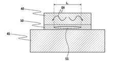
- the solder layer to be formed has a large void longest diameter, for example, as shown in FIG. 3, the heat GH generated from the region located directly above the void 55 in the fluorescent plate 40 is simulated by the void 55.
- the exhaust heat path of the heat GH generated in the fluorescent plate 40 is formed so as to be transmitted to the heat radiating substrate 45 through the side of the void 55, for example, and the heat GH generated in the fluorescent plate 40 is transferred to the heat radiating substrate 45 side. Heat cannot be transferred efficiently. For this reason, there has been a problem that temperature quenching occurs due to a local increase in the temperature of the region located directly above the void 55 in the fluorescent plate 40, and the luminous efficiency is reduced.
- the presence of the void 55 in the solder layer 50 causes a problem that the fluorescence reflectance of the solder layer 50 by the metal solder is lowered, so that the fluorescence intensity emitted from the fluorescent plate 40 is lowered. Furthermore, when the temperature of the fluorescent plate 40 rises, the solder material constituting the solder layer 50 is melted, and there is a problem that the adhesion between the fluorescent plate 40 and the heat dissipation substrate 45 is lowered. It has been found that such a problem becomes prominent when the void ratio in the solder layer 50 is larger than 75% and the longest void diameter L is larger than 0.4 mm.
- the present invention has been made based on the above circumstances, and an object of the present invention is to provide a fluorescent light source device that can obtain a high luminous efficiency and a sufficiently high fluorescence intensity in a fluorescent plate.
- the fluorescent light source device of the present invention includes a fluorescent plate that receives excitation light and emits fluorescence, and a heat radiating substrate that exhausts heat generated in the fluorescent plate, and the fluorescent plate and the heat radiating substrate are joined via a solder layer.
- the void ratio in the solder layer is 75% or less, and the longest void diameter is 0.4 mm or less.
- the void ratio in the solder layer is preferably 50% or less, and the longest void diameter is preferably 0.2 mm or less.
- the fluorescent light source device of the present invention when the void ratio and the longest void diameter in the solder layer are equal to or smaller than a certain size, a good bonding state can be obtained between the fluorescent plate and the heat dissipation substrate. For this reason, it is possible to avoid the separation of the fluorescent plate and the heat dissipation substrate, and it is possible to suppress the extent to which the exhaust heat of the heat generated in the fluorescent plate is inhibited by the void. Therefore, since heat generated in the fluorescent plate can be efficiently exhausted, a local temperature rise of the fluorescent plate can be suppressed, and high luminous efficiency and high fluorescence intensity can be obtained in the fluorescent plate.
- FIG. 1 is an explanatory view schematically showing a configuration example of a fluorescent light emitting member in a fluorescent light source device of the present invention.
- This fluorescent light source apparatus includes a fluorescent light emitting member 10 constituted by a rectangular flat plate-like fluorescent plate 11 that receives excitation light and emits fluorescence, and a rectangular flat plate-shaped heat dissipation substrate 20 that exhausts heat generated in the fluorescent plate 11. I have.
- the back surface of the fluorescent plate 11 whose surface is the excitation light receiving surface 12 is joined to the surface of the heat dissipation substrate 20 via the solder layer 30.
- fluorescence is emitted from the surface of the fluorescent plate 11.
- the excitation light source for example, a laser light source including a semiconductor laser element (LD element) that emits laser light in a blue region having an oscillation wavelength of 455 nm can be used.
- the irradiation condition of the excitation light on the fluorescent plate 11 is, for example, a condition where the excitation light density is 15 to 200 W / mm 2 .
- the fluorescent plate 11 for example, it is preferable to use one having a thermal conductivity of 6 to 35 W / (m ⁇ K).
- a material made of a YAG phosphor doped (activated) with a rare earth compound can be used.
- rare earth compounds include cerium (Ce), praseodymium (Pr), and samarium (Sm).
- the fluorescent plate in which the phosphor contains a metal compound may be used.
- the thickness of the fluorescent plate 11 is, for example, 0.05 to 1 mm.
- a light reflection film 13 made of a metal with high reflectance is formed on the back surface of the fluorescent plate 11.
- the light reflecting film 13 include metal films such as an aluminum (Al) film and a silver (Ag) film, and a reflection enhancing film in which a dielectric multilayer film is formed on the metal film.
- Ni / platinum / gold Ni / Pt / Au
- Ni / Pt / Au nickel / platinum / gold
- a metal film (not shown) made of a nickel / gold (Ni / Au) film is formed.
- a material having a thermal conductivity of 90 W / (m ⁇ K) or more, specifically, for example, 230 to 400 W / (m ⁇ K) is preferably used as the material constituting the heat dissipation substrate 20.
- a material for example, copper, a copper compound (MoCu, CuW, etc.), aluminum, or the like can be used.
- the thickness of the heat dissipation substrate 20 is, for example, 0.5 to 5 mm. Further, from the viewpoint of heat exhaustion and the like, the area of the surface of the heat dissipation substrate 20 is preferably larger than the area of the back surface of the fluorescent plate 11.
- a metal film 21 made of a nickel / gold (Ni / Au) film, for example, formed by a plating method from the viewpoint of bondability with the solder layer 30 is formed.
- solder material constituting the solder layer 30 for example, a material having a thermal conductivity of 40 W / (m ⁇ K) or more, for example, 40 to 70 W / (m ⁇ K) is preferably used.
- a solder material for example, solder such as Sn, Pb or the like mixed with flux or other impurities to form a cream (paste) form, for example, Sn—Ag—Cu solder, Au— Sn-based solder or the like can be used.
- the thickness of the solder layer 30 is, for example, 20 to 200 ⁇ m.
- the void ratio in the solder layer 30 is 75% or less, and the longest void diameter L is 0.4 mm or less.
- the “void ratio” is the ratio of the area of the projected image of the void 35 in plan view (the total area when there are many voids 35) to the total area of the solder layer 30 (the void 35 in the solder layer 30).
- the “void longest diameter” is a size that maximizes the interval between parallel lines when a projected image of the void 35 is sandwiched between two parallel lines in plan view.
- the void ratio and the longest void diameter L in the solder layer 30 can be measured by, for example, an X-ray transmission device.
- the void ratio in the solder layer 30 is 50% or less and the longest void diameter L is 0.2 mm or less.
- the propagation distance to the side of the void 35 can be shortened in the exhaust heat path of the heat GH generated in the region of the fluorescent screen 11 located immediately above the void 35. And the temperature rise of the fluorescent screen 11 can be suppressed reliably.
- the heat GH generated in the fluorescent screen 11 cannot be efficiently exhausted, and the temperature rise in the region located directly above the void 35 in the fluorescent screen 11 is suppressed. Can not do it.
- the longest void length L in the solder layer 30 is larger than 0.4 mm, the heat GH generated in the fluorescent plate 11 cannot be efficiently exhausted, and is located immediately above the void 35 in the fluorescent plate 11. It is impossible to suppress the temperature rise in the area.
- the heat dissipation substrate 20 and the fluorescent plate 11 can be joined as follows.
- the fluorescent plate 11 is disposed on the surface of the heat dissipation substrate 20 via the solder material, and soldering is performed, for example, under reduced pressure in an air atmosphere or a nitrogen gas atmosphere.
- the material is melted by heating to a temperature above its melting point.
- the fluorescent material 11 is joined via the solder layer 30 on the surface of the thermal radiation board
- the solder material when a solder material that does not use a flux is used, the solder material is removed under reduced pressure in an inert gas atmosphere such as a nitrogen gas atmosphere or a mixed gas atmosphere of nitrogen gas and hydrogen gas. It melts by heating to a temperature above its melting point. Then, the fluorescent material 11 is joined via the solder layer 30 on the surface of the thermal radiation board
- the above joining process is performed in the state which pressed the fluorescent plate 11, the solder material, and the thermal radiation board
- the pressure applied to the fluorescent plate 11 during the bonding process is preferably 0 to 2.4 gf / cm 2 , for example.
- the void ratio in the solder layer 30 to be formed can be 75% or less and the longest void diameter L can be 0.4 mm or less.
- the void ratio and the length of the longest void diameter L in the solder layer 30 to be formed can be controlled by adjusting the pressure condition, for example.
- the void ratio and the longest void diameter L in the solder layer 30 constituting the fluorescent light emitting member 10 are equal to or less than a certain size. Since a good bonded state is obtained in the meantime, the degree to which the exhaust heat of the heat generated in the fluorescent screen 11 is inhibited by the void 35 can be suppressed to a small level. For this reason, since heat generated in the fluorescent screen 11 can be efficiently exhausted, a local temperature rise of the fluorescent screen 11 can be suppressed. Therefore, it is possible to avoid the occurrence of temperature quenching associated with the temperature rise of the fluorescent plate 11, so that the fluorescent plate can have high luminous efficiency and sufficiently high emission intensity.
- the heat generated in the fluorescent plate 11 is reliably transferred to the heat dissipation substrate 20. Therefore, the local temperature rise of the fluorescent screen 11 can be reliably suppressed.
- a fluorescent plate (11) having a light reflecting film (13) formed on the back surface is disposed through a ribbon-like solder material having a thermal conductivity of 64.2 W / (m ⁇ K), and the fluorescent plate (11).
- the solder material and its heat-dissipating substrate (20) were pressed with spring-loaded pins while appropriately changing the pressure applied to the fluorescent plate (11) within the range of 0 to 2.4 gf / cm 2 , and the solder material was melted at its melting point. It melted by heating to the above temperature of 218 ° C. After that, the solder material was cooled and solidified to join the fluorescent plate (11) on the surface of the heat dissipation substrate (20) via the solder layer (30).
- a plurality of fluorescent light emitting members (1 ) was prepared.
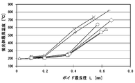
- the thickness of the solder layer (30) in these fluorescent light emitting members (10) is in the range of 20 to 30 ⁇ m, and the void ratio and the longest void diameter (L) in the solder layer (30) are measured by an X-ray transmission device.
- the void ratio was in the range of 0 to 75%, and the longest void diameter (L) was in the range of 0 to 0.62 mm.
- the excitation light receiving surface (12) of the fluorescent plate (11) is irradiated with laser light having an oscillation wavelength of 445 nm from the laser light source.
- the maximum temperature of (11) was measured.
- FIG. 2 a curve indicated by a cross mark, a curve indicated by a cross mark, a curve indicated by a circle mark plot, a curve indicated by a rhombus mark plot, a curve indicated by a triangle mark plot, and a square mark plot
- the curves show the results of the fluorescent light-emitting member (10) in which the void ratio in the solder layer (30) was 75%, 65%, 50%, 35%, 20% and 10%, respectively.
- the maximum temperature of the fluorescent plate (11) is about 200 ° C. It was confirmed that when the longest void diameter (L) was larger than 0.4 mm, the maximum temperature of the fluorescent screen (11) reached 500 ° C. or higher regardless of the void ratio. This is presumably because the void (35) in the solder layer (30) hinders the exhaust of heat generated in the fluorescent screen (11). Further, when the maximum temperature of the fluorescent plate (11) is, for example, 500 ° C. or higher, the maximum temperature of the solder layer (30) is about 400 ° C. or higher, which exceeds the melting point of the solder material. It was confirmed that the adhesion between (20) and the fluorescent screen (11) was lost, causing a problem of detachment.
Landscapes
- Engineering & Computer Science (AREA)
- General Engineering & Computer Science (AREA)
- Chemical & Material Sciences (AREA)
- Physics & Mathematics (AREA)
- Mechanical Engineering (AREA)
- Spectroscopy & Molecular Physics (AREA)
- Materials Engineering (AREA)
- Organic Chemistry (AREA)
- Inorganic Chemistry (AREA)
- Metallurgy (AREA)
- Microelectronics & Electronic Packaging (AREA)
- Optics & Photonics (AREA)
- Electromagnetism (AREA)
- Semiconductor Lasers (AREA)
- Non-Portable Lighting Devices Or Systems Thereof (AREA)
- Arrangement Of Elements, Cooling, Sealing, Or The Like Of Lighting Devices (AREA)
- Securing Globes, Refractors, Reflectors Or The Like (AREA)
Abstract
Description
このような問題は、半田層50におけるボイド率が75%より大きく、また、ボイド最長径Lが0.4mmより大きい場合に顕著に生じるようになることが判明した。
前記半田層におけるボイド率が75%以下であり、ボイド最長径が0.4mm以下であることを特徴とする。
図1は、本発明の蛍光光源装置における蛍光発光部材の一構成例を概略的に示す説明図である。
この蛍光光源装置は、励起光を受けて蛍光を放射する矩形平板状の蛍光板11と、蛍光板11に発生する熱を排熱する矩形平板状の放熱基板20とにより構成された蛍光発光部材10を備えている。この蛍光発光部材10においては、表面が励起光受光面12とされた蛍光板11の裏面が、放熱基板20の表面に対して半田層30を介して接合されている。この蛍光発光部材10においては、蛍光板11の表面から蛍光が放射される。
励起光の蛍光板11に対する照射条件としては、例えば、励起光密度が15~200W/mm2 となる条件である。
蛍光板11の厚みは、例えば0.05~1mmである。
光反射膜13としては、具体的には、アルミニウム(Al)膜および銀(Ag)膜等の金属膜や前記金属膜上に誘電体多層膜を形成した増反射膜などがあげられる。
金属膜の厚みは、例えばNi/Pt/Au=30nm/500nm/500nmである。
放熱基板20の厚みは、例えば0.5~5mmである。
また、排熱性などの観点から、放熱基板20の表面における面積は、蛍光板11の裏面の面積よりも大きいことが好ましい。
半田層30の厚みは、例えば20~200μmである。
ここに、「ボイド率」とは、平面視におけるボイド35の投影像の面積(多数のボイド35がある場合には総面積)の、半田層30の総面積に対する比率(半田層30におけるボイド35の占める面積割合である。また、「ボイド最長径」とは、平面視におけるボイド35の投影像を2本の平行線で挟んだときの当該平行線の間隔が最大となる大きさである。
半田層30におけるボイド率およびボイド最長径Lは、例えばX線透過装置により測定することができる。
また、半田層30におけるボイド率が50%以下とされ、ボイド最長径Lが0.2mm以下とされていることが好ましい。
このような半田層30であることにより、蛍光板11におけるボイド35の直上に位置される領域で発生した熱GHの排熱経路においては、ボイド35側方への伝搬距離を短くすることができるため、蛍光板11の温度上昇を確実に抑制することができる。
また、半田層30におけるボイド最長径Lが0.4mmより大きい場合においても同様に、蛍光板11で生じた熱GHを効率よく排熱することができず、蛍光板11におけるボイド35の直上に位置される領域の温度上昇を抑制することができない。
例えば半田材としてクリーム半田(フラックスを含有)を用いる場合には、放熱基板20の表面上に半田材を介して蛍光板11を配置し、例えば大気雰囲気または窒素ガス雰囲気とされた減圧下において、半田材をその融点以上の温度に加熱して溶融する。その後、当該半田材を冷却して固化することにより、放熱基板20の表面上に半田層30を介して蛍光板11が接合される。
また、例えば半田材としてフラックスを用いないものを用いる場合には、例えば窒素ガス雰囲気などの不活性ガス雰囲気、もしくは窒素ガスと水素ガスとの混合ガス雰囲気とされた減圧下において、半田材をその融点以上の温度に加熱して溶融する。その後、当該半田材を冷却して固化することにより、放熱基板20の表面上に半田層30を介して蛍光板11が接合される。
以上の接合処理は、蛍光板11、半田材および放熱基板20を厚み方向に押圧した状態で行われる。接合処理時における蛍光板11に加えられる圧力は、例えば0~2.4gf/cm2 であることが好ましい。これにより、形成される半田層30におけるボイド率を75%以下、ボイド最長径Lを0.4mm以下とすることができる。形成される半田層30におけるボイド率およびボイド最長径Lの大きさは、例えばこの圧力条件を調整することにより、制御することができる。
30Mo70Cu合金基板よりなる寸法17mm(縦)×17mm(横)×0.47mm(厚み)の放熱基板(20)の表面上に、ニッケル/金(Ni/Au=2500nm/30nm)膜よりなる金属膜(21)を形成した。
処理用チャンバ内において、金属膜(21)が形成された放熱基板(20)の表面上に、Sn(96.5%)Ag(3%)Cu(0.5%)半田(融点=218℃,熱伝導率=64.2W/(m・K)よりなるリボン状の半田材を介して裏面に光反射膜(13)が形成された蛍光板(11)を配置した。そして、蛍光板(11)、半田材および放熱基板(20)を、蛍光板(11)にかける圧力を0~2.4gf/cm2 の範囲内で適宜変更しながらバネ付きのピンによって押圧した状態で、半田材をその融点以上の温度である218℃に加熱して溶融した。その後、半田材を冷却して固化することにより、放熱基板(20)の表面上に半田層(30)を介して蛍光板(11)を接合し、以って、図1に示す構成の複数個の蛍光発光部材(10)を作製した。
これらの蛍光発光部材(10)における半田層(30)の厚みは20~30μmの範囲内であり、半田層(30)におけるボイド率およびボイド最長径(L)をX線透過装置により測定したところ、ボイド率が0~75%の範囲内であり、ボイド最長径(L)が0~0.62mmの範囲内であった。
11 蛍光板
12 励起光受光面
13 光反射膜
20 放熱基板
21 金属膜
30 半田層
35 ボイド
40 蛍光板
45 放熱基板
50 半田層
55 ボイド
Claims (2)
- 励起光を受けて蛍光を放射する蛍光板と、当該蛍光板に発生する熱を排熱する放熱基板とを備え、当該蛍光板と当該放熱基板とが半田層を介して接合されてなる蛍光光源装置において、
前記半田層におけるボイド率が75%以下であり、ボイド最長径が0.4mm以下であることを特徴とする蛍光光源装置。 - 前記半田層におけるボイド率が50%以下であり、ボイド最長径が0.2mm以下であることを特徴とする請求項1に記載の蛍光光源装置。
Priority Applications (3)
| Application Number | Priority Date | Filing Date | Title |
|---|---|---|---|
| CN201680015432.7A CN107407475B (zh) | 2015-03-20 | 2016-02-10 | 荧光光源装置 |
| US15/559,096 US10571107B2 (en) | 2015-03-20 | 2016-02-10 | Fluorescence light source apparatus |
| KR1020177029898A KR101809429B1 (ko) | 2015-03-20 | 2016-02-10 | 형광 광원 장치 |
Applications Claiming Priority (2)
| Application Number | Priority Date | Filing Date | Title |
|---|---|---|---|
| JP2015057054A JP6020631B2 (ja) | 2015-03-20 | 2015-03-20 | 蛍光光源装置 |
| JP2015-057054 | 2015-03-20 |
Publications (1)
| Publication Number | Publication Date |
|---|---|
| WO2016152297A1 true WO2016152297A1 (ja) | 2016-09-29 |
Family
ID=56978419
Family Applications (1)
| Application Number | Title | Priority Date | Filing Date |
|---|---|---|---|
| PCT/JP2016/053921 Ceased WO2016152297A1 (ja) | 2015-03-20 | 2016-02-10 | 蛍光光源装置 |
Country Status (5)
| Country | Link |
|---|---|
| US (1) | US10571107B2 (ja) |
| JP (1) | JP6020631B2 (ja) |
| KR (1) | KR101809429B1 (ja) |
| CN (1) | CN107407475B (ja) |
| WO (1) | WO2016152297A1 (ja) |
Cited By (1)
| Publication number | Priority date | Publication date | Assignee | Title |
|---|---|---|---|---|
| EP4001752A4 (en) * | 2019-07-16 | 2023-12-06 | Ngk Spark Plug Co., Ltd. | Wavelength conversion member, light source device and method for producing wavelength conversion member |
Families Citing this family (5)
| Publication number | Priority date | Publication date | Assignee | Title |
|---|---|---|---|---|
| WO2019097790A1 (ja) | 2017-11-15 | 2019-05-23 | パナソニックIpマネジメント株式会社 | 半導体モジュールおよびその製造方法 |
| JP6768205B2 (ja) * | 2018-05-24 | 2020-10-14 | カシオ計算機株式会社 | 光源装置及び投影装置 |
| JP7312829B2 (ja) * | 2019-07-16 | 2023-07-21 | 日本特殊陶業株式会社 | 半田付け用波長変換部材、波長変換装置、および、光源装置 |
| KR102728880B1 (ko) * | 2020-06-08 | 2024-11-11 | 니혼도꾸슈도교 가부시키가이샤 | 형광판, 파장 변환 부재, 및 광원 장치 |
| JP7588325B2 (ja) * | 2020-12-04 | 2024-11-22 | パナソニックIpマネジメント株式会社 | 蛍光発光素子、蛍光発光モジュール及び発光装置 |
Citations (4)
| Publication number | Priority date | Publication date | Assignee | Title |
|---|---|---|---|---|
| JP2013084960A (ja) * | 2011-10-11 | 2013-05-09 | Led Engin Inc | はんだ接合のための溝付き板 |
| JP2014060164A (ja) * | 2013-10-28 | 2014-04-03 | Sharp Corp | 発光装置、および照明装置 |
| WO2014065051A1 (ja) * | 2012-10-26 | 2014-05-01 | ウシオ電機株式会社 | 蛍光光源装置 |
| JP2015050124A (ja) * | 2013-09-03 | 2015-03-16 | スタンレー電気株式会社 | 発光装置 |
Family Cites Families (8)
| Publication number | Priority date | Publication date | Assignee | Title |
|---|---|---|---|---|
| JP4685245B2 (ja) | 2001-01-09 | 2011-05-18 | 電気化学工業株式会社 | 回路基板及びその製造方法 |
| US7928455B2 (en) * | 2002-07-15 | 2011-04-19 | Epistar Corporation | Semiconductor light-emitting device and method for forming the same |
| US20090014746A1 (en) * | 2007-07-11 | 2009-01-15 | Ainissa Gweneth Ramirez | Solder alloys |
| JP5530165B2 (ja) | 2009-12-17 | 2014-06-25 | スタンレー電気株式会社 | 光源装置および照明装置 |
| JP2012243624A (ja) * | 2011-05-20 | 2012-12-10 | Stanley Electric Co Ltd | 光源装置および照明装置 |
| JP2013247295A (ja) * | 2012-05-28 | 2013-12-09 | Fujitsu Ltd | 導電性接合材料、並びに電子部品及び電子機器 |
| CN102777838B (zh) * | 2012-07-23 | 2014-07-30 | 贵州光浦森光电有限公司 | 一种通用型led灯泡构成方法及液态荧光的led灯泡 |
| CN203434192U (zh) * | 2013-07-12 | 2014-02-12 | 广东洲明节能科技有限公司 | 承载散热板和远程荧光粉结构的led光源 |
-
2015
- 2015-03-20 JP JP2015057054A patent/JP6020631B2/ja active Active
-
2016
- 2016-02-10 CN CN201680015432.7A patent/CN107407475B/zh active Active
- 2016-02-10 US US15/559,096 patent/US10571107B2/en active Active
- 2016-02-10 KR KR1020177029898A patent/KR101809429B1/ko active Active
- 2016-02-10 WO PCT/JP2016/053921 patent/WO2016152297A1/ja not_active Ceased
Patent Citations (4)
| Publication number | Priority date | Publication date | Assignee | Title |
|---|---|---|---|---|
| JP2013084960A (ja) * | 2011-10-11 | 2013-05-09 | Led Engin Inc | はんだ接合のための溝付き板 |
| WO2014065051A1 (ja) * | 2012-10-26 | 2014-05-01 | ウシオ電機株式会社 | 蛍光光源装置 |
| JP2015050124A (ja) * | 2013-09-03 | 2015-03-16 | スタンレー電気株式会社 | 発光装置 |
| JP2014060164A (ja) * | 2013-10-28 | 2014-04-03 | Sharp Corp | 発光装置、および照明装置 |
Non-Patent Citations (1)
| Title |
|---|
| KATSIS D.C. ET AL.: "Void-Induced Thermal Impedance in Power Semiconductor Modules: Some Transient Temperature Effects", IEEE TRANSACTONS ON INDUSTRY APPLICATIONS, vol. 39, no. 5, 2003, pages 1239 - 1246, XP011101764 * |
Cited By (1)
| Publication number | Priority date | Publication date | Assignee | Title |
|---|---|---|---|---|
| EP4001752A4 (en) * | 2019-07-16 | 2023-12-06 | Ngk Spark Plug Co., Ltd. | Wavelength conversion member, light source device and method for producing wavelength conversion member |
Also Published As
| Publication number | Publication date |
|---|---|
| JP2016177979A (ja) | 2016-10-06 |
| US10571107B2 (en) | 2020-02-25 |
| JP6020631B2 (ja) | 2016-11-02 |
| CN107407475B (zh) | 2018-10-02 |
| US20180051871A1 (en) | 2018-02-22 |
| CN107407475A (zh) | 2017-11-28 |
| KR20170123341A (ko) | 2017-11-07 |
| KR101809429B1 (ko) | 2017-12-14 |
Similar Documents
| Publication | Publication Date | Title |
|---|---|---|
| JP6020631B2 (ja) | 蛍光光源装置 | |
| JP6164221B2 (ja) | 蛍光光源装置 | |
| KR101809430B1 (ko) | 형광 광원 장치 | |
| US9318871B2 (en) | Semiconductor laser device and manufacturing method thereof, and submount manufacturing method | |
| CN107429906B (zh) | 荧光光源装置 | |
| JP2017194706A (ja) | 波長変換装置の製造方法 | |
| CN101847821A (zh) | 发光设备及其制造方法 | |
| TW200411955A (en) | Vertical GaN light emitting diode and method for manufacturing the same | |
| JP2014137973A (ja) | 光源装置 | |
| JP4811629B2 (ja) | 半導体レーザ装置 | |
| JP2014029967A (ja) | 半導体装置及びその製造方法 | |
| WO2017064951A1 (ja) | 光源装置 | |
| JP6019758B2 (ja) | 光源装置 | |
| JP2012033589A (ja) | 化合物半導体の製造方法 | |
| JP2012080053A (ja) | 伝導冷却パッケージレーザー及びそのパッケージ方法 | |
| JP2022020424A (ja) | 半導体発光装置 | |
| JP2006351847A (ja) | 半導体発光装置 | |
| JP2006294805A (ja) | 半導体レーザ装置 | |
| CN101341803A (zh) | 用于led基台的多孔电路材料 | |
| WO2013118800A1 (ja) | 半導体装置 | |
| Tsai et al. | Reducing heat crowding in InGaN/GaN flip-chip light-emitting diodes with diamond-like carbon heat-spreading layers | |
| CN120784718A (zh) | 一种基于激光远程激发荧光的大功率光源 | |
| JP2014154570A (ja) | 半導体装置 | |
| JP2006032408A (ja) | 半導体レーザ装置およびその製造方法 | |
| JP2007088114A (ja) | 窒化物半導体レーザ装置の製造方法 |
Legal Events
| Date | Code | Title | Description |
|---|---|---|---|
| 121 | Ep: the epo has been informed by wipo that ep was designated in this application |
Ref document number: 16768200 Country of ref document: EP Kind code of ref document: A1 |
|
| WWE | Wipo information: entry into national phase |
Ref document number: 15559096 Country of ref document: US |
|
| NENP | Non-entry into the national phase |
Ref country code: DE |
|
| ENP | Entry into the national phase |
Ref document number: 20177029898 Country of ref document: KR Kind code of ref document: A |
|
| 122 | Ep: pct application non-entry in european phase |
Ref document number: 16768200 Country of ref document: EP Kind code of ref document: A1 |