WO2016140031A1 - 基板処理方法、コンピュータ記憶媒体及び基板処理システム - Google Patents
基板処理方法、コンピュータ記憶媒体及び基板処理システム Download PDFInfo
- Publication number
- WO2016140031A1 WO2016140031A1 PCT/JP2016/053988 JP2016053988W WO2016140031A1 WO 2016140031 A1 WO2016140031 A1 WO 2016140031A1 JP 2016053988 W JP2016053988 W JP 2016053988W WO 2016140031 A1 WO2016140031 A1 WO 2016140031A1
- Authority
- WO
- WIPO (PCT)
- Prior art keywords
- polymer
- hydrophilic polymer
- block copolymer
- substrate
- coating film
- Prior art date
- Legal status (The legal status is an assumption and is not a legal conclusion. Google has not performed a legal analysis and makes no representation as to the accuracy of the status listed.)
- Ceased
Links
Images









Classifications
-
- B—PERFORMING OPERATIONS; TRANSPORTING
- B81—MICROSTRUCTURAL TECHNOLOGY
- B81C—PROCESSES OR APPARATUS SPECIALLY ADAPTED FOR THE MANUFACTURE OR TREATMENT OF MICROSTRUCTURAL DEVICES OR SYSTEMS
- B81C1/00—Manufacture or treatment of devices or systems in or on a substrate
- B81C1/00015—Manufacture or treatment of devices or systems in or on a substrate for manufacturing microsystems
- B81C1/00023—Manufacture or treatment of devices or systems in or on a substrate for manufacturing microsystems without movable or flexible elements
- B81C1/00031—Regular or irregular arrays of nanoscale structures, e.g. etch mask layer
-
- G—PHYSICS
- G03—PHOTOGRAPHY; CINEMATOGRAPHY; ANALOGOUS TECHNIQUES USING WAVES OTHER THAN OPTICAL WAVES; ELECTROGRAPHY; HOLOGRAPHY
- G03F—PHOTOMECHANICAL PRODUCTION OF TEXTURED OR PATTERNED SURFACES, e.g. FOR PRINTING, FOR PROCESSING OF SEMICONDUCTOR DEVICES; MATERIALS THEREFOR; ORIGINALS THEREFOR; APPARATUS SPECIALLY ADAPTED THEREFOR
- G03F7/00—Photomechanical, e.g. photolithographic, production of textured or patterned surfaces, e.g. printing surfaces; Materials therefor, e.g. comprising photoresists; Apparatus specially adapted therefor
- G03F7/0002—Lithographic processes using patterning methods other than those involving the exposure to radiation, e.g. by stamping
-
- B—PERFORMING OPERATIONS; TRANSPORTING
- B81—MICROSTRUCTURAL TECHNOLOGY
- B81C—PROCESSES OR APPARATUS SPECIALLY ADAPTED FOR THE MANUFACTURE OR TREATMENT OF MICROSTRUCTURAL DEVICES OR SYSTEMS
- B81C1/00—Manufacture or treatment of devices or systems in or on a substrate
- B81C1/00388—Etch mask forming
- B81C1/00428—Etch mask forming processes not provided for in groups B81C1/00396 - B81C1/0042
-
- C—CHEMISTRY; METALLURGY
- C08—ORGANIC MACROMOLECULAR COMPOUNDS; THEIR PREPARATION OR CHEMICAL WORKING-UP; COMPOSITIONS BASED THEREON
- C08F—MACROMOLECULAR COMPOUNDS OBTAINED BY REACTIONS ONLY INVOLVING CARBON-TO-CARBON UNSATURATED BONDS
- C08F297/00—Macromolecular compounds obtained by successively polymerising different monomer systems using a catalyst of the ionic or coordination type without deactivating the intermediate polymer
-
- C—CHEMISTRY; METALLURGY
- C09—DYES; PAINTS; POLISHES; NATURAL RESINS; ADHESIVES; COMPOSITIONS NOT OTHERWISE PROVIDED FOR; APPLICATIONS OF MATERIALS NOT OTHERWISE PROVIDED FOR
- C09D—COATING COMPOSITIONS, e.g. PAINTS, VARNISHES OR LACQUERS; FILLING PASTES; CHEMICAL PAINT OR INK REMOVERS; INKS; CORRECTING FLUIDS; WOODSTAINS; PASTES OR SOLIDS FOR COLOURING OR PRINTING; USE OF MATERIALS THEREFOR
- C09D153/00—Coating compositions based on block copolymers containing at least one sequence of a polymer obtained by reactions only involving carbon-to-carbon unsaturated bonds; Coating compositions based on derivatives of such polymers
-
- H—ELECTRICITY
- H10—SEMICONDUCTOR DEVICES; ELECTRIC SOLID-STATE DEVICES NOT OTHERWISE PROVIDED FOR
- H10P—GENERIC PROCESSES OR APPARATUS FOR THE MANUFACTURE OR TREATMENT OF DEVICES COVERED BY CLASS H10
- H10P72/00—Handling or holding of wafers, substrates or devices during manufacture or treatment thereof
- H10P72/04—Apparatus for manufacture or treatment
- H10P72/0451—Apparatus for manufacturing or treating in a plurality of work-stations
- H10P72/0452—Apparatus for manufacturing or treating in a plurality of work-stations characterised by the layout of the process chambers
- H10P72/0458—Apparatus for manufacturing or treating in a plurality of work-stations characterised by the layout of the process chambers vertical arrangement
-
- H—ELECTRICITY
- H10—SEMICONDUCTOR DEVICES; ELECTRIC SOLID-STATE DEVICES NOT OTHERWISE PROVIDED FOR
- H10P—GENERIC PROCESSES OR APPARATUS FOR THE MANUFACTURE OR TREATMENT OF DEVICES COVERED BY CLASS H10
- H10P72/00—Handling or holding of wafers, substrates or devices during manufacture or treatment thereof
- H10P72/30—Handling or holding of wafers, substrates or devices during manufacture or treatment thereof for conveying, e.g. between different workstations
- H10P72/33—Handling or holding of wafers, substrates or devices during manufacture or treatment thereof for conveying, e.g. between different workstations into and out of processing chamber
- H10P72/3302—Mechanical parts of transfer devices
-
- H—ELECTRICITY
- H10—SEMICONDUCTOR DEVICES; ELECTRIC SOLID-STATE DEVICES NOT OTHERWISE PROVIDED FOR
- H10P—GENERIC PROCESSES OR APPARATUS FOR THE MANUFACTURE OR TREATMENT OF DEVICES COVERED BY CLASS H10
- H10P76/00—Manufacture or treatment of masks on semiconductor bodies, e.g. by lithography or photolithography
-
- H—ELECTRICITY
- H10—SEMICONDUCTOR DEVICES; ELECTRIC SOLID-STATE DEVICES NOT OTHERWISE PROVIDED FOR
- H10P—GENERIC PROCESSES OR APPARATUS FOR THE MANUFACTURE OR TREATMENT OF DEVICES COVERED BY CLASS H10
- H10P76/00—Manufacture or treatment of masks on semiconductor bodies, e.g. by lithography or photolithography
- H10P76/20—Manufacture or treatment of masks on semiconductor bodies, e.g. by lithography or photolithography of masks comprising organic materials
-
- H—ELECTRICITY
- H10—SEMICONDUCTOR DEVICES; ELECTRIC SOLID-STATE DEVICES NOT OTHERWISE PROVIDED FOR
- H10P—GENERIC PROCESSES OR APPARATUS FOR THE MANUFACTURE OR TREATMENT OF DEVICES COVERED BY CLASS H10
- H10P76/00—Manufacture or treatment of masks on semiconductor bodies, e.g. by lithography or photolithography
- H10P76/40—Manufacture or treatment of masks on semiconductor bodies, e.g. by lithography or photolithography of masks comprising inorganic materials
- H10P76/408—Manufacture or treatment of masks on semiconductor bodies, e.g. by lithography or photolithography of masks comprising inorganic materials characterised by their sizes, orientations, dispositions, behaviours or shapes
- H10P76/4085—Manufacture or treatment of masks on semiconductor bodies, e.g. by lithography or photolithography of masks comprising inorganic materials characterised by their sizes, orientations, dispositions, behaviours or shapes characterised by the processes involved to create the masks
-
- B—PERFORMING OPERATIONS; TRANSPORTING
- B81—MICROSTRUCTURAL TECHNOLOGY
- B81C—PROCESSES OR APPARATUS SPECIALLY ADAPTED FOR THE MANUFACTURE OR TREATMENT OF MICROSTRUCTURAL DEVICES OR SYSTEMS
- B81C2201/00—Manufacture or treatment of microstructural devices or systems
- B81C2201/01—Manufacture or treatment of microstructural devices or systems in or on a substrate
- B81C2201/0101—Shaping material; Structuring the bulk substrate or layers on the substrate; Film patterning
- B81C2201/0147—Film patterning
- B81C2201/0149—Forming nanoscale microstructures using auto-arranging or self-assembling material
-
- B—PERFORMING OPERATIONS; TRANSPORTING
- B82—NANOTECHNOLOGY
- B82Y—SPECIFIC USES OR APPLICATIONS OF NANOSTRUCTURES; MEASUREMENT OR ANALYSIS OF NANOSTRUCTURES; MANUFACTURE OR TREATMENT OF NANOSTRUCTURES
- B82Y40/00—Manufacture or treatment of nanostructures
Definitions
- the present invention uses a block copolymer comprising a hydrophilic (polar) polymer having hydrophilicity (polarity) and a hydrophobic (nonpolar) polymer having hydrophobicity (no polarity).
- the present invention relates to a substrate processing method, a computer storage medium, and a substrate processing system.
- a resist coating process is performed by applying a resist solution on a semiconductor wafer (hereinafter referred to as “wafer”) as a substrate, and a predetermined pattern is exposed on the resist film.
- Wafer semiconductor wafer
- a photolithography process for sequentially performing an exposure process and a development process for developing the exposed resist film is performed, and a predetermined resist pattern is formed on the wafer.
- an etching process is performed on the film to be processed on the wafer, and then a resist film removing process is performed to form a predetermined pattern on the film to be processed.
- Patent Document 1 a wafer processing method using a block copolymer composed of a hydrophilic polymer (hydrophilic polymer) and a hydrophobic polymer (hydrophobic polymer) has been proposed (Patent Document 1).
- a hole pattern is formed on the wafer, for example, at a position corresponding to the hexagonal close-packed structure in plan view.
- a circular pattern is formed as a base with a hydrophilic film at a part of the position corresponding to the hexagonal close-packed structure, and a block copolymer is applied on the patterned wafer. .
- the circular pattern having hydrophilicity that has been formed as a base functions as a guide, and has a cylindrical shape so as to be in contact with the upper surface of the pattern.
- a hydrophilic polymer is arranged.
- the hydrophilic polymers are autonomously and regularly arranged sequentially at positions corresponding to the hexagonal close-packed structure.
- a fine hole pattern is formed on the wafer by the hydrophobic polymer.
- the processing target film is etched using the hydrophobic polymer pattern as a mask to form a predetermined pattern on the processing target film.
- the present invention has been made in view of such points, and an object of the present invention is to appropriately form a predetermined pattern on a substrate in substrate processing using a block copolymer containing a hydrophilic polymer and a hydrophobic polymer. It is said.
- one embodiment of the present invention is a method of treating a substrate using a block copolymer including a hydrophilic polymer and a hydrophobic polymer, wherein a neutral layer is formed on the substrate.
- the ratio of the molecular weight of the hydrophilic polymer in the block copolymer is adjusted to 20% to 40% so that the hydrophilic polymer is arranged at a position corresponding to the hexagonal close
- the cylindrical first hydrophilic polymer is phase-separated on each circular pattern by the hydrophobic coating film, and between the first hydrophilic polymers, Cylindrical second hydrophilic polymer is phase-separated so that the first hydrophilic polymer and the second hydrophilic polymer are arranged at positions corresponding to the hexagonal close-packed structure in a plan view.
- the diameter of the circular pattern formed by the conductive coating film is set to 2 (L 0 -R) or less.
- L 0 pitch between the first hydrophilic polymer and the second hydrophilic polymer adjacent to each other
- R radius of the second hydrophilic polymer
- a guide is generally formed on the base with a film having a small energy difference from the polymer whose arrangement is to be controlled, out of a hydrophilic polymer and a hydrophobic polymer, and applied on the block.
- the polymer is autonomously arranged at a position corresponding to the guide.
- the present inventors have found that the arrangement of the polymer can be controlled also by forming a guide with a film having a large energy difference from the polymer to be arranged.
- a circular guide is formed by a film having a large energy difference from the hydrophilic polymer that is the polymer to be arranged, that is, a hydrophobic film
- Hydrophobic polymer is attracted on the guide, but since there is a certain amount of hydrophilic polymer in the block copolymer, it is hydrophilic in the center of the region where the hydrophobic polymer is attracted. It was found that the polymer was aligned.
- the present invention is based on such knowledge, a circular pattern is formed by a hydrophobic coating film at a predetermined position on the substrate, and the molecular weight of the hydrophilic polymer is adjusted to a predetermined ratio on the circular pattern.
- the block copolymer is applied, and then the block copolymer is phase-separated.
- the cylindrical hydrophilic polymer is autonomously arranged at a position corresponding to the center of the circular pattern formed by the hydrophobic coating film.
- the second hydrophilic polymer is arranged at a position corresponding to the hexagonal close-packed structure in plan view by setting the diameter of the circular pattern formed by the hydrophobic coating film to a predetermined value or less. Will be able to.
- the first hydrophilic polymer and the second hydrophilic polymer are located at a position corresponding to the desired pattern, that is, the hexagonal close-packed structure.
- An arrayed pattern can be formed.
- the diameter of the circular pattern formed by the hydrophobic coating film is such that the pitch between the adjacent first hydrophilic polymer and the second hydrophilic polymer is L 0 , and the radius of the second hydrophilic polymer.
- R is 2 (L 0 -R) or less, as in Patent Document 1, compared with the case where a hydrophilic film is used to control the arrangement of a cylindrical hydrophilic polymer. A very large process margin can be secured. Therefore, according to the present invention, a predetermined pattern can be appropriately formed on a substrate in substrate processing using a block copolymer containing a hydrophilic polymer and a hydrophobic polymer.
- Another aspect of the present invention is a method for treating a substrate using a block copolymer including a hydrophilic polymer and a hydrophobic polymer, wherein a neutral layer is formed on the substrate.
- a layer forming step, a coating film pattern forming step of forming a plurality of circular patterns with a hydrophobic coating film at predetermined positions on the substrate after the neutral layer forming step, and a pattern of the coating film are formed.
- the circular pattern formed in the coating film pattern forming step is adjusted to 20% to 40% so that the hydrophilic polymer is arranged at a position corresponding to the hexagonal close-packed structure in plan view, and the circular pattern formed in the following (1 ) To (3).
- the diameter of the circular pattern is 0.8 to 1.5 times the desired pitch between the hydrophilic polymers arranged after the polymer separation step.
- the distance between the adjacent circular patterns adjacent to each other is twice the desired pitch.
- At least one of the circular patterns is arranged on a circumference having the radius of 2 ⁇ 3 times the desired pitch with the circular pattern as the center.
- Another aspect of the present invention is a method of treating a substrate using a block copolymer containing a hydrophilic polymer and a hydrophobic polymer, wherein the neutral layer is formed on the substrate.
- Forming a coating layer pattern, forming a plurality of circular patterns with a hydrophobic coating film at a predetermined position on the substrate after the neutral layer forming step, and forming the coating film pattern A block copolymer coating step of coating the block copolymer on the formed substrate, a polymer separation step of phase-separating the block copolymer into the hydrophilic polymer and the hydrophobic polymer, and the phase separation.
- a polymer removing step of selectively removing the hydrophilic polymer from the block copolymer The ratio of the molecular weight of the hydrophilic polymer in the block copolymer is adjusted to 20% to 40% so that the hydrophilic polymer is arranged at a position corresponding to the hexagonal close-packed structure in a plan view after the polymer separation step.
- the circular pattern formed in the coating film pattern forming step is arranged in a regular triangle shape having a pitch twice as large as a desired pitch between the hydrophilic polymers arranged after the polymer separation step.
- a readable program storing a program that operates on a computer of a control unit that controls the substrate processing system so as to cause the substrate processing system to execute the above-described method for processing each substrate.
- Computer storage medium storing a program that operates on a computer of a control unit that controls the substrate processing system so as to cause the substrate processing system to execute the above-described method for processing each substrate.
- a substrate processing system for processing a substrate using a block copolymer including a hydrophilic polymer and a hydrophobic polymer, wherein the resist has a resist film applied on the substrate.
- a coating apparatus a development processing apparatus for developing a resist film after exposure processing formed on a substrate to form a resist pattern, and a coating film for forming a hydrophobic coating film on the substrate after the resist pattern is formed
- a forming apparatus a resist removing apparatus that removes the resist pattern from the substrate after the coating film is formed; a block copolymer coating apparatus that applies a block copolymer to the substrate after the resist pattern is removed; From a polymer separation device for phase-separating a block copolymer into the hydrophilic polymer and the hydrophobic polymer, and the phase-separated block copolymer, And a polymer removing apparatus for selectively removing the serial hydrophilic polymer.
- the molecular weight ratio of the hydrophilic polymer in the block copolymer applied by the block copolymer coating device is such that the hydrophilic polymer has a hexagonal close-packed structure in plan view after phase separation in the polymer separation device.
- the pattern formed by the coating film and adjusted so as to be arranged at corresponding positions is a circular pattern, and the circular pattern is determined based on the following (1) to (3).
- the diameter of the circular pattern is 0.8 to 1.5 times the desired pitch between hydrophilic polymers arranged after phase separation in the polymer separator.
- the distance between the adjacent circular patterns adjacent to each other is twice the desired pitch.
- At least one of the circular patterns is arranged on a circumference having the radius of 2 ⁇ 3 times the desired pitch with the circular pattern as the center.
- a predetermined pattern can be appropriately formed on a substrate in substrate processing using a block copolymer containing a hydrophilic polymer and a hydrophobic polymer.
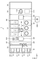
- FIG. 1 is an explanatory diagram showing an outline of the configuration of a substrate processing system 1 that performs the substrate processing method according to the present embodiment.
- 2 and 3 are a front view and a rear view, respectively, schematically showing the outline of the internal configuration of the substrate processing system 1.
- the substrate processing system 1 in the present embodiment is, for example, a coating and developing processing system.
- a case where a predetermined pattern is formed on a film to be processed formed on the upper surface of the wafer W will be described as an example. .
- the substrate processing system 1 includes a cassette station 10 in which a cassette C containing a plurality of wafers W is loaded and unloaded, and a processing station 11 having a plurality of various processing apparatuses for performing predetermined processing on the wafers W. And an interface station 13 that transfers the wafer W to and from the exposure apparatus 12 adjacent to the processing station 11 is integrally connected.
- the cassette station 10 is provided with a cassette mounting table 20.
- the cassette mounting table 20 is provided with a plurality of cassette mounting plates 21 on which the cassette C is mounted when the cassette C is carried into and out of the substrate processing system 1.
- the cassette station 10 is provided with a wafer transfer device 23 that is movable on a transfer path 22 extending in the X direction as shown in FIG.
- the wafer transfer device 23 is also movable in the vertical direction and the vertical axis direction ( ⁇ direction), and includes a cassette C on each cassette mounting plate 21 and a delivery device for a third block G3 of the processing station 11 described later.
- the wafer W can be transferred between the two.
- the processing station 11 is provided with a plurality of, for example, four blocks G1, G2, G3, and G4 having various devices.
- the first block G1 is provided on the front side of the processing station 11 (X direction negative direction side in FIG. 1), and the second block is provided on the back side of the processing station 11 (X direction positive direction side in FIG. 1).
- Block G2 is provided.
- a third block G3 is provided on the cassette station 10 side (Y direction negative direction side in FIG. 1) of the processing station 11, and the interface station 13 side (Y direction positive direction side in FIG. 1) of the processing station 11 is provided. Is provided with a fourth block G4.
- a plurality of liquid processing apparatuses for example, a developing apparatus 30 for developing the wafer W, an organic solvent supply as a polymer removing apparatus for supplying an organic solvent onto the wafer W Apparatus 31, antireflection film forming apparatus 32 for forming an antireflection film on wafer W, neutral layer forming apparatus 33 for forming a neutral layer by applying a neutral agent on wafer W, resist solution on wafer W
- the resist removal device 36 for removing the resist film by supplying the block copolymer and the block copolymer coating device 37 for coating the block copolymer on the wafer W are stacked in order from the bottom.
- the developing device 30, the organic solvent supply device 31, the antireflection film forming device 32, the neutral layer forming device 33, the resist coating device 34, the coating film forming device 35, the resist removing device 36, and the block copolymer coating device 37 are Three are arranged side by side in the horizontal direction. The number and arrangement of these liquid processing apparatuses can be arbitrarily selected.
- spin coating for applying a predetermined coating liquid on the wafer W is performed.
- a coating liquid is discharged onto the wafer W from a coating nozzle, and the wafer W is rotated to diffuse the coating liquid to the surface of the wafer W.
- the block copolymer applied on the wafer W by the block copolymer coating device 37 is a first polymer in which the first monomer and the second monomer are linearly polymerized (the weight of the first monomer).
- a hydrophilic polymer having hydrophilicity (polarity) is used
- a hydrophobic polymer having hydrophobicity (nonpolarity) is used.
- PMMA polymethyl methacrylate
- PS polystyrene
- the molecular weight ratio of the hydrophilic polymer in the block copolymer is about 20% to 40%, and the molecular weight ratio of the hydrophobic polymer in the block copolymer is about 80% to 60%.
- the block copolymer is obtained by making a copolymer of these hydrophilic polymer and hydrophobic polymer into a solution with a solvent.
- the neutral layer formed on the wafer W by the neutral layer forming apparatus 33 has an intermediate affinity for the hydrophilic polymer and the hydrophobic polymer.
- a random copolymer or an alternating copolymer of polymethyl methacrylate and polystyrene is used as the neutralizing agent.
- neutral means having an intermediate affinity for the hydrophilic polymer and the hydrophobic polymer.
- a heat treatment apparatus 40 for performing heat treatment of the wafer W an ultraviolet irradiation apparatus 41 for irradiating the wafer W with ultraviolet light, an adhesion apparatus 42 for hydrophobizing the wafer W, A peripheral exposure device 43 that exposes the outer peripheral portion of the wafer W, and a polymer separation device 44 that phase-separates the block copolymer applied on the wafer W by the block copolymer coating device 37 into a hydrophilic polymer and a hydrophobic polymer Are arranged side by side in the horizontal direction.
- the heat treatment apparatus 40 includes a hot plate for placing and heating the wafer W and a cooling plate for placing and cooling the wafer W, and can perform both heat treatment and cooling treatment.
- the polymer separation device 44 is also a device that performs heat treatment on the wafer W, and the configuration thereof is the same as that of the heat treatment device 40.
- the ultraviolet irradiation device 41 includes a mounting table on which the wafer W is mounted, and an ultraviolet irradiation unit that irradiates the wafer W on the mounting table with ultraviolet light having a wavelength of 172 nm, for example.
- the number and arrangement of the heat treatment apparatus 40, the ultraviolet irradiation apparatus 41, the adhesion apparatus 42, the peripheral exposure apparatus 43, and the polymer separation apparatus 44 can be arbitrarily selected.
- a plurality of delivery devices 50, 51, 52, 53, 54, 55, 56 are provided in order from the bottom.
- the fourth block G4 is provided with a plurality of delivery devices 60, 61, 62 in order from the bottom.
- a wafer transfer area D is formed in an area surrounded by the first block G1 to the fourth block G4.
- a plurality of wafer transfer devices 70 having transfer arms that are movable in the Y direction, the X direction, the ⁇ direction, and the vertical direction are arranged.
- the wafer transfer device 70 moves in the wafer transfer area D and transfers the wafer W to a predetermined device in the surrounding first block G1, second block G2, third block G3, and fourth block G4. it can.
- a shuttle transfer device 80 that transfers the wafer W linearly between the third block G3 and the fourth block G4 is provided.
- the shuttle transport device 80 is linearly movable in the Y direction, for example.
- the shuttle transfer device 80 moves in the Y direction while supporting the wafer W, and can transfer the wafer W between the transfer device 52 of the third block G3 and the transfer device 62 of the fourth block G4.
- a wafer transfer device 100 is provided next to the third block G3 on the positive side in the X direction.
- the wafer transfer apparatus 100 has a transfer arm that is movable in the X direction, the ⁇ direction, and the vertical direction, for example.
- the wafer transfer device 100 can move up and down while supporting the wafer W, and can transfer the wafer W to each delivery device in the third block G3.
- the interface station 13 is provided with a wafer transfer device 110 and a delivery device 111.
- the wafer transfer device 110 has a transfer arm that is movable in the Y direction, the ⁇ direction, and the vertical direction, for example.
- the wafer transfer device 110 can transfer the wafer W between each transfer device, the transfer device 111, and the exposure device 12 in the fourth block G4, for example, by supporting the wafer W on a transfer arm.
- the substrate processing system 1 described above is provided with a control unit 300 as shown in FIG.
- the control unit 300 is a computer, for example, and has a program storage unit (not shown).
- the program storage unit stores a program for controlling the processing of the wafer W in the substrate processing system 1.
- the program storage unit also stores a program for controlling the operation of driving systems such as the above-described various processing apparatuses and transfer apparatuses to realize wafer processing in the substrate processing system 1.
- the program is recorded on a computer-readable storage medium H such as a computer-readable hard disk (HD), a flexible disk (FD), a compact disk (CD), a magnetic optical desk (MO), or a memory card. May have been installed in the control unit 300 from the storage medium.
- HD computer-readable hard disk
- FD flexible disk
- CD compact disk
- MO magnetic optical desk
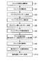
- FIG. 4 is a flowchart showing an example of main steps of such wafer processing.
- a cassette C storing a plurality of wafers W is carried into the cassette station 10 of the substrate processing system 1, and each wafer W in the cassette C is sequentially transferred to the transfer device 53 of the processing station 11 by the wafer transfer device 23. .
- the wafer W is transferred to the heat treatment apparatus 40 and the temperature is adjusted, and then transferred to the antireflection film forming apparatus 32 to form an antireflection film 400 on the wafer W as shown in FIG. 5 (FIG. 4).
- Step S1 Note that the film to be processed E is previously formed on the upper surface of the wafer W as described above on the wafer W in the present embodiment, and the antireflection film 400 is formed on the upper surface of the film to be processed E. Thereafter, the wafer W is transferred to the heat treatment apparatus 40, heated, and the temperature is adjusted.
- the wafer W is transported to the neutral layer forming apparatus 33, and a neutral agent is applied on the antireflection film 400 of the wafer W to form a neutral layer 401 as shown in FIG. Layer formation step, step S2 in FIG. Thereafter, the wafer W is transferred to the heat treatment apparatus 40, heated, and the temperature is adjusted.
- the wafer W is transferred to the adhesion apparatus 42 and subjected to an adhesion process. Thereafter, the wafer W is transported to the resist coating unit 34, and a resist solution is applied onto the neutral layer 401 of the wafer W to form a resist film 402 as shown in FIG. Thereafter, the wafer W is transferred to the heat treatment apparatus 40 and pre-baked. Thereafter, the wafer W is transferred to the peripheral exposure device 43 and subjected to peripheral exposure processing.
- the wafer W is transferred to the exposure apparatus 12 by the wafer transfer apparatus 110 of the interface station 13 and subjected to exposure processing. Thereafter, the wafer W is transferred to the heat treatment apparatus 40 and subjected to post-exposure baking. Thereafter, the wafer W is transferred to the developing device 30 and developed. After completion of the development, the wafer W is transferred to the heat treatment apparatus 40 and subjected to a post baking process.
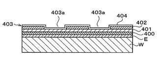
- a predetermined resist pattern 403 is formed by the resist film 402 on the neutral layer 401 of the wafer W (step S3 in FIG. 4).
- the resist pattern 403 in the present embodiment is a pattern in which circular hole portions 403a having a diameter Q are arranged at positions corresponding to the hexagonal close-packed structure in plan view. That is, the distance between the centers of the hole portions 403a (pitch P in FIG. 6) is the same, and the three adjacent hole portions 403a are arranged in an equilateral triangle shape.
- the pitch P in the present embodiment is about 80 nm, for example.
- the diameter Q of the hole portion 403a is set to approximately 0.4 to 0.75 times the pitch P, and is 60 nm, which is approximately 0.75 times the pitch P in this embodiment. The basis for setting the diameter Q of the hole portion 403a will be described later.
- the wafer W is transferred to the coating film forming apparatus 35.
- the coating liquid is supplied onto the wafer W on which the resist pattern 403 is formed.
- the coating solution one having a hydrophobic property, in other words, a hydrophilic polymer and a hydrophobic polymer in the block copolymer having a small energy difference from the hydrophobic polymer is used.
- the coating solution applied by the coating film forming apparatus 35 is, for example, a solution of polystyrene in a solvent form.
- a polystyrene film 404 is formed as a hydrophobic coating film on the resist pattern 403 (step S4 in FIG. 4).
- two hole portions 403a are illustrated in an enlarged manner.
- the wafer W is transferred to the resist removing device 36.
- a resist removing liquid is supplied onto the wafer W, and the resist pattern 403 by the resist film 402 is removed.
- the resist removing solution for example, a mixed solution of an organic amine and a polar solvent is used.
- the resist pattern 403 is removed, the polystyrene film 404 formed in the hole portion 403a of the resist pattern 403 remains on the neutral layer 401.
- a circular pattern is formed on the neutral layer 401 of the wafer W by the polystyrene film 404 with the same diameter Q and pitch P as the hole portions 403a of the resist pattern 403 (coating film).
- Pattern formation step, step S5 in FIG. Accordingly, the circular pattern formed by the polystyrene film 404 is in a state in which the pitch P between the adjacent polystyrene films 404 is arranged in a uniform triangular shape, like the hole portion 403a of the resist pattern 403.
- the wafer W is transferred to the block copolymer coating device 37.
- a block copolymer 410 is coated on the wafer W (block copolymer coating step; step S6 in FIG. 4).
- the wafer W is transferred to the polymer separation device 44 and subjected to heat treatment at a predetermined temperature.
- the block copolymer 410 on the wafer W is phase-separated into a hydrophilic polymer and a hydrophobic polymer (polymer separation step; step S7 in FIG. 4).
- the molecular weight ratio of the hydrophilic polymer in the block copolymer 410 is 20% to 40%, and the molecular weight ratio of the hydrophobic polymer is 80% to 60%.
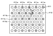
- the cylindrical hydrophilic polymers 411 are arranged at equal intervals, and the hydrophilic polymer 411 is phase-separated so as to surround the hydrophobic polymer 412.
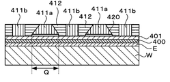
- the hydrophobic polymer 412 after the phase separation is on the polystyrene film 404 having a smaller energy difference than the neutral layer 401 as shown in FIG. 12. And is arranged so as to be in contact with the polystyrene film 404.
- the hydrophilic polymer 411 is present in the block copolymer 410 at a ratio of 20% to 40%, the hydrophilic polymer 411 is arranged in a more energetically stable position. As a result, as shown in FIG. 12, the hydrophilic polymer 411 is arranged at a position corresponding to the center of the circular polystyrene film 404.
- a gap Z may be formed between the hydrophilic polymer 411 and the polystyrene film 404.
- the code of the hydrophilic polymer arranged at the position corresponding to the center of the circular polystyrene film 404 is “411a”, and the code of the other hydrophilic polymer is “411b”.
- the hydrophilic polymer denoted by “411a” is referred to as a first hydrophilic polymer
- the hydrophilic polymer denoted by “411b” is referred to as a second hydrophilic polymer.
- the second hydrophilic polymer 411b is arranged in a region other than the circular polystyrene film 404.
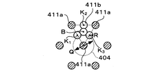
- the second hydrophilic polymer 411b is arranged in a stable position in terms of energy, and as a result, as shown in FIGS. Are arranged at a middle position between the adjacent circular polystyrene films 404. In other words, they are arranged at positions between the first hydrophilic polymers 411a on the circular polystyrene film 404.
- the pitch L 0 between the adjacent first hydrophilic polymer 411 a and the second hydrophilic polymer 411 b is half of the pitch P between the polystyrene films 404.
- the pitch L 0 and the diameters of the first hydrophilic polymer 411a and the second hydrophilic polymer 411b are interaction parameters between the hydrophilic polymer 411 and the hydrophobic polymer 412 constituting the block copolymer 410. It is determined by a certain ⁇ (chi) parameter and the molecular weight of each polymer.
- the pitch P of the polystyrene film 404 pattern i.e., the pitch P of the hole portion 403a of the resist pattern 403 is determined based on the pitch L 0 as determined by tests conducted beforehand. In other words, to determine the desired ratio of the hydrophilic polymer 411 and the hydrophobic polymer 412 in the block copolymer 410 so that the pitch L 0 is obtained, on the pitch P based on the desired pitch L 0 To decide.
- the second hydrophilic polymer 411b is arranged at an intermediate position between the first hydrophilic polymers 411a located on the center of the polystyrene film 404.
- the range is limited to the three first hydrophilic polymers 411a as positions where the distances are equal to the adjacent first hydrophilic polymers 411a, as shown in FIG.
- the positions of the centroids B of the three first hydrophilic polymers 411a are listed.
- the second hydrophilic polymer 411b is arranged at the positions of the energy-stable midpoints K 1 , K 2 , K 3 .
- the diameter Q of the pattern of the polystyrene film 404 is set so as to overlap with the second hydrophilic polymer 411b located at the midpoints K 1 and K 3 in a plan view, for example, as indicated by a dashed circle in FIG.
- the midpoints K 1 and K 3 are not in an energetically stable position.
- the second hydrophilic polymer 411b is arranged not at the midpoints K 1 and K 3 but at the position of the center of gravity B in order to reduce the energy difference.
- the hydrophilic polymer 411 rotates 30 degrees in an arbitrary direction as compared with the case shown in FIG.
- the second hydrophilic polymer 411b is arranged at each of the midpoints K 1 , K 2 , K 3 , for example.
- the hydrophilic polymers 411 are arranged at positions where the pitch L 0 is 2 ⁇ 3 / 3 times.
- the diameter Q of the pattern of the polystyrene film 404 is set to 2 (L 0 -R) or less, so that each of the midpoints K 1 , K 2 , K 3 second hydrophilic polymer 411b is an array, whereby the pitch of the hydrophilic polymer 411 after the sequence may be L 0 in.
- the pitch of each hydrophilic polymer 411 after the sequence desired to be 2 ⁇ 3 / 3 times the L 0 is when the 2 ⁇ 3 / 3 times the pitch of the L 0 and L 1
- the diameter Q of the pattern may be greater than 2 (L 0 -R) and 2 (L 1 -R) or less. That is, the pitch can be changed between the pitch L 0 and the pitch L 1 while arranging the hydrophilic polymers 411 at positions corresponding to the hexagonal close-packed structure according to the set value of the diameter Q.
- the diameter Q of the pattern of the polystyrene film 404 is preferably 2 (L 0 -R) or less as described above.
- the diameter Q of the pattern of the polystyrene film 404 is more preferably 1.5 times or less of the desired pitch L 0 and 0.75 times or less of the pitch P when the pitch P of the pattern of the polystyrene film 404 is used as a reference. It was confirmed. Therefore, the diameter Q in the present embodiment is set to 60 nm, which is 0.75 times the pitch P.
- the hydrophilic polymer 411 From the viewpoint of arranging the hydrophilic polymer 411 at a desired pitch L 0 , it is not necessary to provide a lower limit for the diameter Q of the pattern of the polystyrene film 404, but according to the present inventors, the polystyrene film It is confirmed that the value of the gap Z formed between the first hydrophilic polymer 411a and the polystyrene film 404 shown in FIG. . Therefore, from the viewpoint of using the hydrophobic polymer 412 as an etching mask, the gap Z is preferably as small as possible.
- the diameter Q is generally 0.8 times the desired pitch L 0 of the cylindrical pattern with a hydrophilic polymer 411 It can be said that it is preferable to set it to ⁇ 1.5 times or 0.4 times to 0.75 times pitch P. Therefore, when the desired pitch L 0 is 40 nm as in the present embodiment, the diameter Q may be about 32 nm to 60 nm and has a process margin of about 30 nm.
- Patent Document 1 when a circular pattern with a hydrophilic coating film is used as a guide for arranging the hydrophilic polymers 411, the process for the pattern diameter Q as described above is used.
- the margin is very small.
- the guide is formed by the hydrophilic coating film 420, the first hydrophilic polymer 411a after the phase separation is arranged so as to be in contact with the coating film 420 having a small energy difference. Therefore, when the diameter Q is larger than the diameter of the desired hydrophilic polymer 411, it becomes a truncated cone shape in which the diameter expands downward.
- the diameter Q When the diameter Q is excessive, the first hydrophilic polymer 411a is not exposed on the upper surface of the hydrophobic polymer 412, and has a substantially truncated cone shape. In such a case, in the etching using the hydrophobic polymer 412 as a mask, the processing target film E cannot be processed with a desired dimension. Therefore, the diameter Q needs to be approximately the same as or smaller than the diameter of the cylindrical hydrophilic polymer 411 after phase separation. However, generally, there is an unavoidable error of about 5 nm in the dimension (CD: Critical Dimension) of the resist pattern 403, but the diameter of the hydrophilic polymer 411 is approximately 20 nm to 30 nm. For the diameter, this error is so large that it cannot be ignored.
- CD Critical Dimension
- the wafer W is transferred to the ultraviolet irradiation device 41.
- the ultraviolet irradiation device 41 irradiates the wafer W with ultraviolet rays to break the polymethyl methacrylate bond chain, which is the hydrophilic polymer 411, and causes the polystyrene, which is the hydrophobic polymer 412, to undergo a crosslinking reaction (step of FIG. 4). S8).
- the wafer W is transferred to the organic solvent supply device 31.
- a polar organic solvent polar organic solvent
- IPA isopropyl alcohol
- the hydrophilic polymer 411 whose bond chain has been cut by ultraviolet irradiation is dissolved by the organic solvent, and the hydrophilic polymer 411 is selectively removed from the wafer W (polymer removal step; step S9 in FIG. 4).
- a hole pattern 430 is formed by the hydrophobic polymer 412.
- the wafer W is transferred to the delivery device 50 by the wafer transfer device 70, Thereafter, the wafer is transferred to the cassette C of the predetermined cassette mounting plate 21 by the wafer transfer device 23 of the cassette station 10.
- the cassette C is transferred to an etching processing apparatus (not shown) provided outside the substrate processing system 1, and the neutral layer 401, the antireflection film 400, and the processing target film E are formed using the hydrophobic polymer 412 as a mask. Etched. Thereby, as shown in FIG. 16, the hole pattern 430 is transferred to the film E to be processed (step S10 in FIG. 4). During etching, the hydrophobic polymer 412 and the polystyrene film 404 remain in the hole pattern 430 formed by the first hydrophilic polymer 411a, but the gap Z and the thickness of the polystyrene film 404 are appropriately adjusted.
- etching processing apparatus for example, an RIE (Reactive Ion Etching) apparatus is used. That is, in the etching processing apparatus, dry etching for etching a film to be processed such as a hydrophilic polymer or an antireflection film is performed by a reactive gas (etching gas), ions, or radicals.
- RIE Reactive Ion Etching
- the wafer W is etched again, and the hydrophobic polymer 412, the neutral layer 401 and the antireflection film 400 on the wafer W are removed. Thereafter, the wafer W is unloaded from the etching processing apparatus, and a series of wafer processing ends.
- a circular pattern is formed on the wafer W by the polystyrene film 404 which is a hydrophobic film, and then the block copolymer 410 is applied, and then the block copolymer 410 is applied. Therefore, the cylindrical first hydrophilic polymer 411a is autonomously arranged at a position corresponding to the center of the circular pattern formed by the polystyrene film 404. At this time, by setting the diameter Q of the pattern of the polystyrene film 404 to 2 (L 0 -R) or less, the second hydrophilic polymer 411b is autonomously positioned at an intermediate position between the first hydrophilic polymers 411a. Array.
- the hydrophilic polymer 411 is arranged at a position corresponding to the hexagonal close-packed structure in a plan view at a pitch L 0 that is half the pitch P of each polystyrene film 404 formed on the wafer W. Therefore, a predetermined pattern is formed on the wafer W while ensuring a very large process margin in the dimension of the diameter Q as compared with the case where a hydrophilic film is used to control the arrangement of the cylindrical hydrophilic polymer 411. Can be formed appropriately.
- the diameter Q of the circular pattern formed by the polystyrene film 404 is 0.8 to 1.5 of the desired pitch L 0 between the hydrophilic polymers 411 after the phase separation of the block copolymer 410. It may be doubled.
- the second hydrophilic polymer arranged between the first hydrophilic polymers 411a by setting the diameter Q of the pattern of the polystyrene film 404. Since arrangement
- the second hydrophilic polymer 411b is arranged so as to fill the space between the polymers 411a. This is because when the film formed on the surface of the wafer W in contact with the block copolymer 410 is a hydrophilic coating film 420 and a neutral layer 401, it is located at any position of the neutral layer 401 from the viewpoint of energy. This is because the second hydrophilic polymer 411b can be arranged. Therefore, in order to determine the arrangement of the second hydrophilic polymer 411b, it is necessary to first form the columnar first hydrophilic polymer 411a on the coating film 420. For this reason, the time required for the heat treatment for phase separation becomes longer, and as a result, the throughput of the wafer processing decreases.
- the second hydrophilic polymer 411b having a large energy difference is not arranged inside the circular pattern of the polystyrene film 404 having a diameter Q shown in FIG. That is, the second hydrophilic polymer 411b is naturally arranged at any one of the midpoints K 1 , K 2 , K 3 or the center of gravity B. Then, as described above, by appropriately setting the diameter Q, it is possible to induce the arrangement of the second hydrophilic polymer 411b to the midpoint K 1, K 2, K 3 . As a result, the arrangement of the second hydrophilic polymer 411b can be determined quickly, thereby shortening the time required for the heat treatment for phase separation and consequently improving the throughput of the wafer processing.
- the ratio of the molecular weight of the hydrophilic polymer is about 20% to 40%.
- the ratio between the first hydrophilic polymer 411a and the polystyrene film 404 is From the standpoint of setting the value of the gap Z formed in the desired value, the ratio of the molecular weight of the hydrophilic polymer 411 in the block copolymer 410 is 32% to 34%, and the ratio of the molecular weight of the hydrophobic polymer 412 is It has been confirmed that 68% to 66% is more preferable.
- the hydrophilic polymer 411 does not come into contact with the polystyrene film 404 and is energetic. First, it moves above the center of the polystyrene film 404, which is a stable position. That is, as shown in FIG. 12, the island of the first hydrophilic polymer 411a floats in the sea of the hydrophobic polymer 412.
- the first hydrophilic polymer 411a above the center of the polystyrene film 404 becomes adjacent to the second hydrophilic polymer 411a.
- the diameter of the upper surface of the first hydrophilic polymer 411a is reduced so that the distance between the 411b and the 411b is constant (in terms of energy stability), and changes to a substantially cylindrical shape as a whole. Even if the diameter of the upper surface of the first hydrophilic polymer 411a is reduced, the volume of the island of the first hydrophilic polymer 411a does not change. Move to.
- the value of the gap Z is determined by the degree of downward movement of the first hydrophilic polymer 411a in the thickness direction of the wafer W.
- the volume of the islands of the first hydrophilic polymer 411a is one of the factors that determine how much the first hydrophilic polymer 411a moves downward in the thickness direction of the wafer W.
- the volume of the island of one hydrophilic polymer 411a depends on the ratio of the molecular weight of the hydrophilic polymer in the block copolymer 410. Therefore, the value of the gap Z can be adjusted by adjusting the ratio of the molecular weight of the hydrophilic polymer in the block copolymer 410. According to the present inventors, the value is set to 32% to 34% as described above. It is preferable.
- the factor determining the gap Z includes the film thickness of the block copolymer 410 formed in step S6. According to the above, it has been confirmed that this film thickness is preferably about 0.4 to 0.6 times the desired pitch L 0 between the hydrophilic polymers 411.
- the circular polystyrene film 404 functioning as a guide is arranged in an equilateral triangle shape.
- the hydrophilic polymer 411 is arranged at a position corresponding to the hexagonal close-packed structure in a plan view
- the polystyrene film 404 is arranged.
- the arrangement of is not limited to the contents of the present embodiment. For example, as shown in FIG. 17, among the seven adjacent coordinates U1 to U7 constituting the hexagonal close-packed structure, for example, by deleting the hole portion 403a of the coordinates of U7 located at the center, a polystyrene film is formed at the coordinates U7.
- the pitch P between the adjacent adjacent hole portions 403a is set to the desired pitch of the hydrophilic polymer 411. set the double L 0, and around any of the hole portions 403a, radius on 2 ⁇ 3 times the circumference of the pitch L 0, if such at least one hole portion 403a is arranged Good.
- the polystyrene film 404 is applied on the resist pattern 403, and then the resist pattern 403 is removed, whereby the polystyrene film 404 is formed on the neutral layer 401.
- the method of forming the circular pattern by the polystyrene film 404 is not limited to the contents of the present embodiment.
- a polystyrene film 404 is applied on the neutral layer 401, then a resist pattern 403 is formed on the polystyrene film 404, and the polystyrene film 404 is etched using the resist pattern 403 as a mask.
- a pattern by the polystyrene film 404 may be formed.
- the case where the resist pattern 403 is transferred to the film E to be processed on the wafer W has been described as an example.
- the wafer W is etched to form a ball-shaped pattern on the wafer W. It can also be applied to the case of transferring.
- the removal of the resist pattern 403 in the step S5 and the removal of the hydrophilic polymer 411 in the step S9 are performed by so-called wet treatment.
- the technique for removing the resist pattern 403 and the hydrophilic polymer 411 is the present method.
- the above-described dry etching or the like may be used. That is, instead of the resist removing device 36 and the organic solvent supply device 31 as the polymer removing device, a dry etching device may be used.
- the present invention is not limited to such examples. It is obvious for those skilled in the art that various changes or modifications can be conceived within the scope of the idea described in the claims, and these are naturally within the technical scope of the present invention. It is understood.
- the present invention is not limited to this example and can take various forms.
- the present invention can also be applied to a case where the substrate is another substrate such as an FPD (flat panel display) other than a wafer or a mask reticle for a photomask.
- FPD flat panel display
- the present invention is useful when a substrate is treated with a block copolymer containing, for example, a hydrophilic polymer having hydrophilicity and a hydrophobic polymer having hydrophobicity.
Landscapes
- Chemical & Material Sciences (AREA)
- Engineering & Computer Science (AREA)
- Manufacturing & Machinery (AREA)
- Nanotechnology (AREA)
- Chemical Kinetics & Catalysis (AREA)
- Organic Chemistry (AREA)
- Physics & Mathematics (AREA)
- General Physics & Mathematics (AREA)
- Microelectronics & Electronic Packaging (AREA)
- Health & Medical Sciences (AREA)
- Inorganic Chemistry (AREA)
- Medicinal Chemistry (AREA)
- Polymers & Plastics (AREA)
- Crystallography & Structural Chemistry (AREA)
- Condensed Matter Physics & Semiconductors (AREA)
- Wood Science & Technology (AREA)
- Materials Engineering (AREA)
- Life Sciences & Earth Sciences (AREA)
- Analytical Chemistry (AREA)
- Exposure Of Semiconductors, Excluding Electron Or Ion Beam Exposure (AREA)
- Photosensitive Polymer And Photoresist Processing (AREA)
- Application Of Or Painting With Fluid Materials (AREA)
- Graft Or Block Polymers (AREA)
- Robotics (AREA)
Abstract
Description
本願は、2015年3月5日に日本国に出願された特願2015-043551号に基づき、優先権を主張し、その内容をここに援用する。
(1)前記円形状のパターンの直径は、前記ポリマー分離工程後に配列する親水性ポリマー間の所望のピッチの0.8~1.5倍である。
(2)隣り合う最も近い前記円形状のパターン間の距離は、前記所望のピッチの2倍である。
(3)前記円形状のパターンを中心とした、半径が前記所望のピッチの2√3倍の円周上に、少なくとも1つの前記円形状のパターンが配置される。
(1)前記円形状のパターンの直径は、前記ポリマー分離装置での相分離後に配列する親水性ポリマー間の所望のピッチの0.8~1.5倍である。
(2)隣り合う最も近い前記円形状のパターン間の距離は、前記所望のピッチの2倍である。
(3)前記円形状のパターンを中心とした、半径が前記所望のピッチの2√3倍の円周上に、少なくとも1つの前記円形状のパターンが配置される。
その後カセットステーション10のウェハ搬送装置23によって所定のカセット載置板21のカセットCに搬送される。
30 現像装置
31 有機溶剤供給装置
32 反射防止膜形成装置
33 中性層形成装置
34 レジスト塗布装置
35 塗布膜形成装置
36 レジスト除去装置
37 ブロック共重合体塗布装置
40 熱処理装置
41 紫外線照射装置
42 アドヒージョン装置
43 周辺露光装置
44 ポリマー分離装置
300 制御部
400 反射防止膜
401 中性層
402 レジスト膜
403 レジストパターン
404 ポリスチレン膜
410 ブロック共重合体
411 親水性ポリマー
412 疎水性ポリマー
W ウェハ
Claims (10)
- 親水性ポリマーと疎水性ポリマーとを含むブロック共重合体を用いて、基板を処理する基板処理方法であって、
前記基板上に中性層を形成する中性層形成工程と、
前記中性層形成工程後の基板上の所定の位置に、疎水性の塗布膜により円形状のパターンを複数形成する塗布膜パターン形成工程と、
前記塗布膜のパターンが形成された基板上に前記ブロック共重合体を塗布するブロック共重合体塗布工程と、
前記のブロック共重合体を前記親水性ポリマーと前記疎水性ポリマーに相分離させるポリマー分離工程と、
前記相分離したブロック共重合体から、前記親水性ポリマーを選択的に除去するポリマー除去工程を有し、
前記ブロック共重合体における前記親水性ポリマーの分子量の比率は、前記ポリマー分離工程後に前記親水性ポリマーが平面視において六方最密構造に対応する位置に配列するように20%~40%に調整され、
前記ポリマー分離工程において、前記疎水性の塗布膜による円形状の各パターン上に円柱状の第1の親水性ポリマーをそれぞれ相分離させると共に、当該各第1の親水性ポリマーの間に、円柱状の第2の親水性ポリマーを相分離させて、前記第1の親水性ポリマーと前記第2の親水性ポリマーが平面視において六方最密構造に対応する位置に配列するように、前記疎水性の塗布膜による円形状のパターンの直径は、2(L0-R)以下に設定されている。
L0:隣り合う前記第1の親水性ポリマーと前記第2の親水性ポリマー間のピッチ
R:前記第2の親水性ポリマーの半径 - 親水性ポリマーと疎水性ポリマーとを含むブロック共重合体を用いて、基板を処理する基板処理方法であって、
前記基板上に中性層を形成する中性層形成工程と
前記中性層形成工程後の基板上の所定の位置に、疎水性の塗布膜により円形状のパターンを複数形成する塗布膜パターン形成工程と、
前記塗布膜のパターンが形成された基板上に前記ブロック共重合体を塗布するブロック共重合体塗布工程と、
前記のブロック共重合体を前記親水性ポリマーと前記疎水性ポリマーに相分離させるポリマー分離工程と、
前記相分離したブロック共重合体から、前記親水性ポリマーを選択的に除去するポリマー除去工程を有し、
前記ブロック共重合体における前記親水性ポリマーの分子量の比率は、前記ポリマー分離工程後に前記親水性ポリマーが平面視において六方最密構造に対応する位置に配列するように20%~40%に調整され、
前記塗布膜パターン形成工程において形成される円形状のパターンは、以下の(1)~(3)に基づいて定められる。
(1)前記円形状のパターンの直径は、前記ポリマー分離工程後に配列する親水性ポリマー間の所望のピッチの0.8~1.5倍である。
(2)隣り合う最も近い前記円形状のパターン間の距離は、前記所望のピッチの2倍である。
(3)前記円形状のパターンを中心とした、半径が前記所望のピッチの2√3倍の円周上に、少なくとも1つの前記円形状のパターンが配置される。 - 親水性ポリマーと疎水性ポリマーとを含むブロック共重合体を用いて、基板を処理する基板処理方法であって、
前記基板上に中性層を形成する中性層形成工程と、
前記中性層形成工程後の基板上の所定の位置に、疎水性の塗布膜により円形状のパターンを複数形成する塗布膜パターン形成工程と、
前記塗布膜のパターンが形成された基板上に前記ブロック共重合体を塗布するブロック共重合体塗布工程と、
前記のブロック共重合体を前記親水性ポリマーと前記疎水性ポリマーに相分離させるポリマー分離工程と、
前記相分離したブロック共重合体から、前記親水性ポリマーを選択的に除去するポリマー除去工程を有し、
前記ブロック共重合体における前記親水性ポリマーの分子量の比率は、前記ポリマー分離工程後に前記親水性ポリマーが平面視において六方最密構造に対応する位置に配列するように20%~40%に調整され、
前記塗布膜パターン形成工程において形成される円形状のパターンは、前記ポリマー分離工程後に配列する親水性ポリマー間の所望のピッチの2倍のピッチを有する正三角形状に配置される。 - 請求項1に記載の基板処理方法において、
前記ブロック共重合体における前記親水性ポリマーの分子量の比率は、32%~34%である。 - 請求項1に記載の基板処理方法において、
前記親水性ポリマーはポリメタクリル酸メチルであり、
前記疎水性ポリマーはポリスチレンである。 - 請求項1に記載の基板処理方法において、
前記疎水性の塗布膜は、ポリスチレン膜である。 - 基板処理方法を基板処理システムによって実行させるように、当該基板処理システムを制御する制御部のコンピュータ上で動作するプログラムを格納した読み取り可能なコンピュータ記憶媒体であって、
前記基板処理方法は、
前記基板上に中性層を形成する中性層形成工程と、
前記中性層形成工程後の基板上の所定の位置に、疎水性の塗布膜により円形状のパターンを複数形成する塗布膜パターン形成工程と、
前記塗布膜のパターンが形成された基板上に前記ブロック共重合体を塗布するブロック共重合体塗布工程と、
前記のブロック共重合体を前記親水性ポリマーと前記疎水性ポリマーに相分離させるポリマー分離工程と、
前記相分離したブロック共重合体から、前記親水性ポリマーを選択的に除去するポリマー除去工程を有し、
前記ブロック共重合体における前記親水性ポリマーの分子量の比率は、前記ポリマー分離工程後に前記親水性ポリマーが平面視において六方最密構造に対応する位置に配列するように20%~40%に調整され、
前記ポリマー分離工程において、前記疎水性の塗布膜による円形状の各パターン上に円柱状の第1の親水性ポリマーをそれぞれ相分離させると共に、当該各第1の親水性ポリマーの間に、円柱状の第2の親水性ポリマーを相分離させて、前記第1の親水性ポリマーと前記第2の親水性ポリマーが平面視において六方最密構造に対応する位置に配列するように、前記疎水性の塗布膜による円形状のパターンの直径は、2(L0-R)以下に設定されている。
L0:隣り合う前記第1の親水性ポリマーと前記第2の親水性ポリマー間のピッチ
R:前記第2の親水性ポリマーの半径 - 基板処理方法を基板処理システムによって実行させるように、当該基板処理システムを制御する制御部のコンピュータ上で動作するプログラムを格納した読み取り可能なコンピュータ記憶媒体であって、
前記基板処理方法は、
前記基板上に中性層を形成する中性層形成工程と
前記中性層形成工程後の基板上の所定の位置に、疎水性の塗布膜により円形状のパターンを複数形成する塗布膜パターン形成工程と、
前記塗布膜のパターンが形成された基板上に前記ブロック共重合体を塗布するブロック共重合体塗布工程と、
前記のブロック共重合体を前記親水性ポリマーと前記疎水性ポリマーに相分離させるポリマー分離工程と、
前記相分離したブロック共重合体から、前記親水性ポリマーを選択的に除去するポリマー除去工程を有し、
前記ブロック共重合体における前記親水性ポリマーの分子量の比率は、前記ポリマー分離工程後に前記親水性ポリマーが平面視において六方最密構造に対応する位置に配列するように20%~40%に調整され、
前記塗布膜パターン形成工程において形成される円形状のパターンは、以下の(1)~(3)に基づいて定められる。
(1)前記円形状のパターンの直径は、前記ポリマー分離工程後に配列する親水性ポリマー間の所望のピッチの0.8~1.5倍である。
(2)隣り合う最も近い前記円形状のパターン間の距離は、前記所望のピッチの2倍である。
(3)前記円形状のパターンを中心とした、半径が前記所望のピッチの2√3倍の円周上に、少なくとも1つの前記円形状のパターンが配置される。 - 基板処理方法を基板処理システムによって実行させるように、当該基板処理システムを制御する制御部のコンピュータ上で動作するプログラムを格納した読み取り可能なコンピュータ記憶媒体であって、
前記基板処理方法は、
前記基板上に中性層を形成する中性層形成工程と、
前記中性層形成工程後の基板上の所定の位置に、疎水性の塗布膜により円形状のパターンを複数形成する塗布膜パターン形成工程と、
前記塗布膜のパターンが形成された基板上に前記ブロック共重合体を塗布するブロック共重合体塗布工程と、
前記のブロック共重合体を前記親水性ポリマーと前記疎水性ポリマーに相分離させるポリマー分離工程と、
前記相分離したブロック共重合体から、前記親水性ポリマーを選択的に除去するポリマー除去工程を有し、
前記ブロック共重合体における前記親水性ポリマーの分子量の比率は、前記ポリマー分離工程後に前記親水性ポリマーが平面視において六方最密構造に対応する位置に配列するように20%~40%に調整され、
前記塗布膜パターン形成工程において形成される円形状のパターンは、前記ポリマー分離工程後に配列する親水性ポリマー間の所望のピッチの2倍のピッチを有する正三角形状に配置される。 - 親水性ポリマーと疎水性ポリマーとを含むブロック共重合体を用いて、基板を処理する基板処理システムであって、
基板上にレジスト膜を塗布するレジスト塗布装置と、
基板上に形成された露光処理後のレジスト膜を現像してレジストパターンを形成する現像処理装置と、
前記レジストパターン形成後の基板に対して疎水性の塗布膜を形成する塗布膜形成装置と、
前記塗布膜形成後の基板から前記レジストパターンを除去するレジスト除去装置と、
前記レジストパターン除去後の基板に対してブロック共重合体を塗布するブロック共重合体塗布装置と、
前記のブロック共重合体を前記親水性ポリマーと前記疎水性ポリマーに相分離させるポリマー分離装置と、
前記相分離したブロック共重合体から、前記親水性ポリマーを選択的に除去するポリマー除去装置を有し、
前記ブロック共重合体における前記親水性ポリマーの分子量の比率は、前記ポリマー分離装置での相分離後に前記親水性ポリマーが平面視において六方最密構造に対応する位置に配列するように20%~40%に調整され、
前記ポリマー分離装置において、前記疎水性の塗布膜による円形状の各パターン上に円柱状の第1の親水性ポリマーをそれぞれ相分離させると共に、当該各第1の親水性ポリマーの間に、円柱状の第2の親水性ポリマーを相分離させて、前記第1の親水性ポリマーと前記第2の親水性ポリマーが平面視において六方最密構造に対応する位置に配列するように、前記疎水性の塗布膜による円形状のパターンの直径は、2(L0-R)以下に設定されている。
L0:隣り合う前記第1の親水性ポリマーと前記第2の親水性ポリマー間のピッチ
R:前記第2の親水性ポリマーの半径
Priority Applications (2)
| Application Number | Priority Date | Filing Date | Title |
|---|---|---|---|
| US15/554,026 US10329144B2 (en) | 2015-03-05 | 2016-02-10 | Substrate treatment method, computer storage medium and substrate treatment system |
| KR1020177024151A KR102510734B1 (ko) | 2015-03-05 | 2016-02-10 | 기판 처리 방법, 컴퓨터 기억 매체 및 기판 처리 시스템 |
Applications Claiming Priority (2)
| Application Number | Priority Date | Filing Date | Title |
|---|---|---|---|
| JP2015-043551 | 2015-03-05 | ||
| JP2015043551A JP6267143B2 (ja) | 2015-03-05 | 2015-03-05 | 基板処理方法、プログラム、コンピュータ記憶媒体及び基板処理システム |
Publications (1)
| Publication Number | Publication Date |
|---|---|
| WO2016140031A1 true WO2016140031A1 (ja) | 2016-09-09 |
Family
ID=56847443
Family Applications (1)
| Application Number | Title | Priority Date | Filing Date |
|---|---|---|---|
| PCT/JP2016/053988 Ceased WO2016140031A1 (ja) | 2015-03-05 | 2016-02-10 | 基板処理方法、コンピュータ記憶媒体及び基板処理システム |
Country Status (5)
| Country | Link |
|---|---|
| US (1) | US10329144B2 (ja) |
| JP (1) | JP6267143B2 (ja) |
| KR (1) | KR102510734B1 (ja) |
| TW (1) | TWI645251B (ja) |
| WO (1) | WO2016140031A1 (ja) |
Families Citing this family (2)
| Publication number | Priority date | Publication date | Assignee | Title |
|---|---|---|---|---|
| KR102031825B1 (ko) * | 2018-03-07 | 2019-10-15 | 한국과학기술원 | 용액재료의 자발적 상분리와 선택적 젖음을 이용한 미세패턴 제조방법 |
| JP7133451B2 (ja) * | 2018-11-30 | 2022-09-08 | 株式会社Screenホールディングス | 基板処理装置 |
Citations (4)
| Publication number | Priority date | Publication date | Assignee | Title |
|---|---|---|---|---|
| JP2010056257A (ja) * | 2008-08-28 | 2010-03-11 | Hitachi Ltd | 微細構造体の製造方法 |
| JP2010123239A (ja) * | 2008-11-19 | 2010-06-03 | Seagate Technology Llc | 直接アドレス指定可能アレイへの自己集合化材料を用いた化学的ピニング |
| JP2010144120A (ja) * | 2008-12-22 | 2010-07-01 | Kyoto Univ | 高分子薄膜及びパターン媒体並びにこれらの製造方法 |
| WO2014038420A1 (ja) * | 2012-09-07 | 2014-03-13 | 東京エレクトロン株式会社 | 基板処理方法、コンピュータ記憶媒体及び基板処理システム |
Family Cites Families (12)
| Publication number | Priority date | Publication date | Assignee | Title |
|---|---|---|---|---|
| US8168284B2 (en) * | 2005-10-06 | 2012-05-01 | Wisconsin Alumni Research Foundation | Fabrication of complex three-dimensional structures based on directed assembly of self-assembling materials on activated two-dimensional templates |
| JP5414011B2 (ja) | 2006-05-23 | 2014-02-12 | 国立大学法人京都大学 | 微細構造体、パターン媒体、及びそれらの製造方法 |
| JP4654279B2 (ja) * | 2008-08-28 | 2011-03-16 | 株式会社日立製作所 | 微細構造を有する高分子薄膜およびパターン基板の製造方法 |
| US9478429B2 (en) * | 2012-03-13 | 2016-10-25 | Massachusetts Institute Of Technology | Removable templates for directed self assembly |
| JP6081728B2 (ja) * | 2012-07-30 | 2017-02-15 | 東京エレクトロン株式会社 | 基板処理方法、コンピュータ記憶媒体及び基板処理システム |
| JP2014063908A (ja) * | 2012-09-21 | 2014-04-10 | Tokyo Electron Ltd | 基板処理システム |
| JP6141144B2 (ja) * | 2012-10-02 | 2017-06-07 | 東京エレクトロン株式会社 | 基板処理方法、プログラム、コンピュータ記憶媒体及び基板処理システム |
| WO2014139793A1 (en) * | 2013-03-15 | 2014-09-18 | Asml Netherlands B.V. | Methods for providing lithography features on a substrate by self-assembly of block copolymers |
| US10884333B2 (en) * | 2013-08-06 | 2021-01-05 | Asml Netherlands B.V. | Method of designing lithography features by self-assembly of block copolymer |
| CN105705997B (zh) * | 2013-11-08 | 2020-01-17 | Asml荷兰有限公司 | 生成用于定向自组装的引导模板的方法 |
| KR20150101875A (ko) * | 2014-02-27 | 2015-09-04 | 삼성전자주식회사 | 블록 공중합체를 이용한 미세 패턴 형성 방법 |
| US20160122580A1 (en) * | 2014-10-30 | 2016-05-05 | Az Electronic Materials (Luxembourg) S.A.R.L. | Defect reduction methods and composition for via formation in directed self-assembly patterning |
-
2015
- 2015-03-05 JP JP2015043551A patent/JP6267143B2/ja active Active
-
2016
- 2016-02-10 US US15/554,026 patent/US10329144B2/en active Active
- 2016-02-10 KR KR1020177024151A patent/KR102510734B1/ko active Active
- 2016-02-10 WO PCT/JP2016/053988 patent/WO2016140031A1/ja not_active Ceased
- 2016-02-23 TW TW105105319A patent/TWI645251B/zh active
Patent Citations (4)
| Publication number | Priority date | Publication date | Assignee | Title |
|---|---|---|---|---|
| JP2010056257A (ja) * | 2008-08-28 | 2010-03-11 | Hitachi Ltd | 微細構造体の製造方法 |
| JP2010123239A (ja) * | 2008-11-19 | 2010-06-03 | Seagate Technology Llc | 直接アドレス指定可能アレイへの自己集合化材料を用いた化学的ピニング |
| JP2010144120A (ja) * | 2008-12-22 | 2010-07-01 | Kyoto Univ | 高分子薄膜及びパターン媒体並びにこれらの製造方法 |
| WO2014038420A1 (ja) * | 2012-09-07 | 2014-03-13 | 東京エレクトロン株式会社 | 基板処理方法、コンピュータ記憶媒体及び基板処理システム |
Also Published As
| Publication number | Publication date |
|---|---|
| KR102510734B1 (ko) | 2023-03-15 |
| US20180065843A1 (en) | 2018-03-08 |
| TW201715295A (zh) | 2017-05-01 |
| JP6267143B2 (ja) | 2018-01-24 |
| TWI645251B (zh) | 2018-12-21 |
| JP2016163010A (ja) | 2016-09-05 |
| US10329144B2 (en) | 2019-06-25 |
| KR20170122199A (ko) | 2017-11-03 |
Similar Documents
| Publication | Publication Date | Title |
|---|---|---|
| JP5919210B2 (ja) | 基板処理方法、プログラム、コンピュータ記憶媒体及び基板処理システム | |
| JP6072644B2 (ja) | 紫外線照射装置、基板処理方法、プログラム及びコンピュータ記憶媒体 | |
| JP2014187103A (ja) | 基板処理装置、基板処理方法、プログラム及びコンピュータ記憶媒体 | |
| JP6267143B2 (ja) | 基板処理方法、プログラム、コンピュータ記憶媒体及び基板処理システム | |
| JP2014027228A (ja) | 基板処理方法、プログラム、コンピュータ記憶媒体及び基板処理システム | |
| JP6081728B2 (ja) | 基板処理方法、コンピュータ記憶媒体及び基板処理システム | |
| KR102268930B1 (ko) | 기판 처리 방법, 판독 가능한 컴퓨터 기억 매체 및 기판 처리 시스템 | |
| JP5881565B2 (ja) | 基板処理方法、プログラム及びコンピュータ記憶媒体 | |
| JP5837525B2 (ja) | 基板処理方法、プログラム及びコンピュータ記憶媒体 | |
| JP6494446B2 (ja) | 基板処理方法、プログラム及びコンピュータ記憶媒体 | |
| JP6678183B2 (ja) | 基板処理方法及びコンピュータ記憶媒体 | |
| WO2016047493A1 (ja) | 基板処理方法、コンピュータ記憶媒体及び基板処理システム | |
| WO2014046241A1 (ja) | 基板処理システム | |
| JP5847738B2 (ja) | 基板処理方法、プログラム及びコンピュータ記憶媒体 | |
| JP2007188925A (ja) | 基板処理方法 | |
| JPWO2017221683A1 (ja) | 基板処理方法、読み取り可能なコンピュータ記憶媒体及び基板処理システム |
Legal Events
| Date | Code | Title | Description |
|---|---|---|---|
| 121 | Ep: the epo has been informed by wipo that ep was designated in this application |
Ref document number: 16758726 Country of ref document: EP Kind code of ref document: A1 |
|
| WWE | Wipo information: entry into national phase |
Ref document number: 15554026 Country of ref document: US |
|
| ENP | Entry into the national phase |
Ref document number: 20177024151 Country of ref document: KR Kind code of ref document: A |
|
| NENP | Non-entry into the national phase |
Ref country code: DE |
|
| 122 | Ep: pct application non-entry in european phase |
Ref document number: 16758726 Country of ref document: EP Kind code of ref document: A1 |