WO2016129304A1 - 薄膜デバイス - Google Patents
薄膜デバイス Download PDFInfo
- Publication number
- WO2016129304A1 WO2016129304A1 PCT/JP2016/050477 JP2016050477W WO2016129304A1 WO 2016129304 A1 WO2016129304 A1 WO 2016129304A1 JP 2016050477 W JP2016050477 W JP 2016050477W WO 2016129304 A1 WO2016129304 A1 WO 2016129304A1
- Authority
- WO
- WIPO (PCT)
- Prior art keywords
- thin film
- resin layer
- constraining
- thin
- substrate
- Prior art date
- Legal status (The legal status is an assumption and is not a legal conclusion. Google has not performed a legal analysis and makes no representation as to the accuracy of the status listed.)
- Ceased
Links
Images




Classifications
-
- H—ELECTRICITY
- H10—SEMICONDUCTOR DEVICES; ELECTRIC SOLID-STATE DEVICES NOT OTHERWISE PROVIDED FOR
- H10D—INORGANIC ELECTRIC SEMICONDUCTOR DEVICES
- H10D89/00—Aspects of integrated devices not covered by groups H10D84/00 - H10D88/00
- H10D89/60—Integrated devices comprising arrangements for electrical or thermal protection, e.g. protection circuits against electrostatic discharge [ESD]
- H10D89/601—Integrated devices comprising arrangements for electrical or thermal protection, e.g. protection circuits against electrostatic discharge [ESD] for devices having insulated gate electrodes, e.g. for IGFETs or IGBTs
- H10D89/911—Integrated devices comprising arrangements for electrical or thermal protection, e.g. protection circuits against electrostatic discharge [ESD] for devices having insulated gate electrodes, e.g. for IGFETs or IGBTs using passive elements as protective elements
-
- H—ELECTRICITY
- H10—SEMICONDUCTOR DEVICES; ELECTRIC SOLID-STATE DEVICES NOT OTHERWISE PROVIDED FOR
- H10D—INORGANIC ELECTRIC SEMICONDUCTOR DEVICES
- H10D1/00—Resistors, capacitors or inductors
- H10D1/40—Resistors
- H10D1/47—Resistors having no potential barriers
-
- H—ELECTRICITY
- H10—SEMICONDUCTOR DEVICES; ELECTRIC SOLID-STATE DEVICES NOT OTHERWISE PROVIDED FOR
- H10D—INORGANIC ELECTRIC SEMICONDUCTOR DEVICES
- H10D1/00—Resistors, capacitors or inductors
- H10D1/60—Capacitors
- H10D1/68—Capacitors having no potential barriers
- H10D1/692—Electrodes
- H10D1/711—Electrodes having non-planar surfaces, e.g. formed by texturisation
- H10D1/716—Electrodes having non-planar surfaces, e.g. formed by texturisation having vertical extensions
-
- H—ELECTRICITY
- H10—SEMICONDUCTOR DEVICES; ELECTRIC SOLID-STATE DEVICES NOT OTHERWISE PROVIDED FOR
- H10D—INORGANIC ELECTRIC SEMICONDUCTOR DEVICES
- H10D84/00—Integrated devices formed in or on semiconductor substrates that comprise only semiconducting layers, e.g. on Si wafers or on GaAs-on-Si wafers
-
- H—ELECTRICITY
- H10—SEMICONDUCTOR DEVICES; ELECTRIC SOLID-STATE DEVICES NOT OTHERWISE PROVIDED FOR
- H10D—INORGANIC ELECTRIC SEMICONDUCTOR DEVICES
- H10D84/00—Integrated devices formed in or on semiconductor substrates that comprise only semiconducting layers, e.g. on Si wafers or on GaAs-on-Si wafers
- H10D84/01—Manufacture or treatment
- H10D84/02—Manufacture or treatment characterised by using material-based technologies
- H10D84/03—Manufacture or treatment characterised by using material-based technologies using Group IV technology, e.g. silicon technology or silicon-carbide [SiC] technology
- H10D84/038—Manufacture or treatment characterised by using material-based technologies using Group IV technology, e.g. silicon technology or silicon-carbide [SiC] technology using silicon technology, e.g. SiGe
-
- H—ELECTRICITY
- H10—SEMICONDUCTOR DEVICES; ELECTRIC SOLID-STATE DEVICES NOT OTHERWISE PROVIDED FOR
- H10D—INORGANIC ELECTRIC SEMICONDUCTOR DEVICES
- H10D89/00—Aspects of integrated devices not covered by groups H10D84/00 - H10D88/00
- H10D89/60—Integrated devices comprising arrangements for electrical or thermal protection, e.g. protection circuits against electrostatic discharge [ESD]
- H10D89/601—Integrated devices comprising arrangements for electrical or thermal protection, e.g. protection circuits against electrostatic discharge [ESD] for devices having insulated gate electrodes, e.g. for IGFETs or IGBTs
- H10D89/611—Integrated devices comprising arrangements for electrical or thermal protection, e.g. protection circuits against electrostatic discharge [ESD] for devices having insulated gate electrodes, e.g. for IGFETs or IGBTs using diodes as protective elements
-
- H—ELECTRICITY
- H10—SEMICONDUCTOR DEVICES; ELECTRIC SOLID-STATE DEVICES NOT OTHERWISE PROVIDED FOR
- H10P—GENERIC PROCESSES OR APPARATUS FOR THE MANUFACTURE OR TREATMENT OF DEVICES COVERED BY CLASS H10
- H10P14/00—Formation of materials, e.g. in the shape of layers or pillars
- H10P14/40—Formation of materials, e.g. in the shape of layers or pillars of conductive or resistive materials
-
- H—ELECTRICITY
- H10—SEMICONDUCTOR DEVICES; ELECTRIC SOLID-STATE DEVICES NOT OTHERWISE PROVIDED FOR
- H10W—GENERIC PACKAGES, INTERCONNECTIONS, CONNECTORS OR OTHER CONSTRUCTIONAL DETAILS OF DEVICES COVERED BY CLASS H10
- H10W20/00—Interconnections in chips, wafers or substrates
- H10W20/01—Manufacture or treatment
-
- H—ELECTRICITY
- H10—SEMICONDUCTOR DEVICES; ELECTRIC SOLID-STATE DEVICES NOT OTHERWISE PROVIDED FOR
- H10W—GENERIC PACKAGES, INTERCONNECTIONS, CONNECTORS OR OTHER CONSTRUCTIONAL DETAILS OF DEVICES COVERED BY CLASS H10
- H10W20/00—Interconnections in chips, wafers or substrates
- H10W20/40—Interconnections external to wafers or substrates, e.g. back-end-of-line [BEOL] metallisations or vias connecting to gate electrodes
-
- H—ELECTRICITY
- H10—SEMICONDUCTOR DEVICES; ELECTRIC SOLID-STATE DEVICES NOT OTHERWISE PROVIDED FOR
- H10W—GENERIC PACKAGES, INTERCONNECTIONS, CONNECTORS OR OTHER CONSTRUCTIONAL DETAILS OF DEVICES COVERED BY CLASS H10
- H10W20/00—Interconnections in chips, wafers or substrates
- H10W20/40—Interconnections external to wafers or substrates, e.g. back-end-of-line [BEOL] metallisations or vias connecting to gate electrodes
- H10W20/495—Capacitive arrangements or effects of, or between wiring layers
- H10W20/496—Capacitor integral with wiring layers
-
- H—ELECTRICITY
- H10—SEMICONDUCTOR DEVICES; ELECTRIC SOLID-STATE DEVICES NOT OTHERWISE PROVIDED FOR
- H10W—GENERIC PACKAGES, INTERCONNECTIONS, CONNECTORS OR OTHER CONSTRUCTIONAL DETAILS OF DEVICES COVERED BY CLASS H10
- H10W20/00—Interconnections in chips, wafers or substrates
- H10W20/40—Interconnections external to wafers or substrates, e.g. back-end-of-line [BEOL] metallisations or vias connecting to gate electrodes
- H10W20/498—Resistive arrangements or effects of, or between, wiring layers
Definitions
- the present invention relates to a thin film device including a thin film resistance element.
- the conventional thin film device 500 shown in FIG. 7 is provided between an integrated circuit 502 formed on a semiconductor substrate 501, a plurality of electrode pads 503 arranged on the integrated circuit 502, and each electrode pad 503. And a resin layer 505 formed on the passivation film 504.
- the resin layer 505 is formed of polyimide resin, epoxy resin, or the like, and a through hole is provided at a position overlapping the electrode pad 503 of the resin layer 505.
- a rewiring 507 connected to the electrode pad 503 through the barrier metal layer 506 in the through hole is formed on the resin layer 505.
- a thin film resistance element 508 is provided at a position between the rewiring 507 on the resin layer 505.
- the thin film resistance element 508 includes a barrier metal layer 506 and a seed layer 509 stacked on the barrier metal layer 506.
- the barrier metal layer 506 is formed of Ti, TiN, Ni, or the like, and is provided to improve the adhesion between the electrode pad 503 and the rewiring 507.
- the seed layer 509 functions as an electrode when the rewiring 507 is formed by a plating method, and is formed of Cu, Al, or the like.
- the resistance value of the thin film resistive element 508 is adjusted by adjusting the film thicknesses of the barrier metal layer 506 and the seed layer 509 as appropriate.
- JP 2009-267248 A (paragraphs 0012, 0016, 0017, FIG. 1, etc.)
- the thin film device 500 shown in FIG. 7 when the thin film device 500 shown in FIG. 7 is heated in a thermal cycle when mounted on another substrate or the like, a bending stress is applied to the thin film resistance element 508 due to expansion of the resin layer 505, etc.
- the thin film resistance element 508 may be damaged.
- the present invention has been made in view of the above-described problems, and can prevent a thin film resistive element from being damaged by a stress or the like caused by expansion of a resin layer, thereby obtaining a highly reliable thin film device.
- the purpose is to provide technology.
- a thin film device of the present invention includes a substrate and a plurality of resin layers laminated on one main surface side of the substrate, and the plurality of resin layers are formed by a thin film formation process.
- a first resin layer in which the formed thin film resistance element is provided on one main surface; and a first constraining thin film formed by a thin film formation process, disposed on the opposite side of the first resin layer from the substrate. Includes a second resin layer provided on one main surface, and the thin film resistor element and the first constraining thin film are arranged so as to overlap in a plan view.
- the first resin layer on which the thin film resistance element is formed has a coefficient of thermal expansion.
- the second resin layer disposed on the opposite side of the first resin layer to the side opposite to the small substrate is expanded to the thin film resistor element formed on the first resin layer in plan view.
- the first constraining thin film is formed so as to overlap with each other. Accordingly, since the thin film resistance element is pressed against the substrate by the first constraining thin film and the resin layer expands at a high temperature state, the bending stress applied to the thin film resistance element can be relaxed. It is possible to prevent the thin film resistance element from being damaged by the stress generated by the expansion of the layer.
- a thin film electrode for wiring formed by a thin film formation process and electrically connected to the thin film resistance element may be formed on one main surface of the second resin layer.
- the first constraining thin film can be formed using the same material by the same thin film forming process as the wiring thin film electrode, the process for forming the first constraining thin film is performed. It is possible to provide a highly reliable thin film device in which cracks and disconnections of a thin film resistor element are prevented by using a conventional manufacturing process without increasing the manufacturing process.
- first constraining thin film and the wiring thin film electrode may be formed separately.
- the first constraining thin film and the wiring thin film electrode may be integrally formed.
- the plurality of resin layers are arranged on the substrate side of the first resin layer, and a third resin layer provided with a second constraining thin film formed by a thin film forming process on one main surface is provided.
- the thin film resistor element and the second constraining thin film may be arranged so as to overlap in plan view.
- a thin film resistive element will be in the state pinched
- the thin film resistor element may contain Si.
- a resistor element and a second thin film resistor element having one end connected to the fourth external electrode, and the thin film capacitor element is inserted between the other ends of the first and second thin film resistor elements.
- the other end of each of the first and second thin film resistor elements may be connected to both ends of the thin film capacitor element.
- the capacitance of the thin film capacitor element is adjusted by adjusting the voltage between the third and fourth external electrodes and arbitrarily adjusting the voltage applied to both ends of the thin film capacitor element via the first and second thin film resistor elements. Can be adjusted.
- an ESD protection element that forms a current path that does not pass through the first and second thin film resistor elements and the thin film capacitor element when an electrostatic discharge of a predetermined voltage or higher occurs may be further provided.
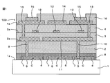
- FIG. 1 and FIG. 2 only the main configuration according to the present invention is shown for simplicity of explanation. 4 to 6 to be referred to in the following description, only the main components are shown as in FIGS. 1 and 2, but the description thereof is omitted in the following description.
- the thin film device 100 includes a substrate 1 such as a glass substrate, a ceramic substrate, a resin substrate, a Si substrate (Si linear expansion coefficient: 3.4 ⁇ 10 ⁇ 6 / K), a GaAs substrate, and the one main surface 1a side of the substrate 1.
- the thin film capacitor element C includes a capacitor electrode layer 5 formed of a Pt thin film in a predetermined region on one main surface 1a of the substrate 1, a (Ba, Sr) TiO 3 (hereinafter referred to as “BST”) dielectric layer 6 and And a capacitor electrode layer 7 formed of a Pt thin film on the BST dielectric layer 6.
- the thin film capacitor element C is covered with a protective layer 8 formed of a SiO 2 moisture-resistant protective film, and the resin layer 2 is laminated on the protective layer 8.
- a capacitor electrode on the upper side of the thin film capacitor element C is formed through a protective layer 8 and a through hole formed in the resin layer 2.
- Cu / Ti extraction electrode 10 connected to capacitor electrode layer 5 on the lower side of thin film capacitor element C, and second constraining thin film 11 are formed. Yes.
- the second constraining thin film 11 is formed simultaneously with the extraction electrodes 9 and 10 using the same material by the same thin film forming process.
- the resin layer 3 is laminated on the resin layer 2 so as to cover the extraction electrodes 9 and 10 and the second constraining thin film 11.
- the second constraining thin film 11 and the extraction electrode 10 are integrally formed, but the second constraining thin film 11 and the extraction electrode 10 may be formed separately.
- the second constraining thin film 11 may be formed integrally with the other extraction electrode formed on the one main surface 2a of the resin layer 2.
- Each of the thin film resistance elements R1 and R2 is one main layer of the resin layer 3 (corresponding to the “first resin layer” of the present invention) (linear expansion coefficient of the resin layer 3: 54.0 ⁇ 10 ⁇ 6 / K) It is formed of a resistive thin film 12 mainly composed of Ni, Cr, and Si formed by a thin film forming process in a predetermined region of the surface 3a.
- a resistive thin film 12 mainly composed of Ni, Cr, and Si formed by a thin film forming process in a predetermined region of the surface 3a.
- all of the thin film resistance elements R1 and R2 are formed on the resin layer 3.
- the thin film resistance elements R1 and R2 are respectively distributed on different resin layers. May be.
- Each thin film resistance element R1, R2 (resistance thin film 12) is covered with a resin layer 4 laminated on one main surface 3a of the resin layer 3. Further, the resin layer 4 (corresponding to the “second resin layer” of the present invention) (the linear expansion coefficient of the resin layer 4: 54.0 ⁇ 10 ⁇ 6 / K) is provided on one main surface 4a with the resin layer 3, Cu / Ti lead electrode 13 (corresponding to the “thin film electrode for wiring” of the present invention) electrically connected to the lead electrodes 9 and 10 and the thin film resistor elements R1 to R13 through the through holes formed in FIG.
- the first constraining thin film 14 is formed simultaneously with the extraction electrode 13 using the same material by the same thin film forming process.
- the first constraining thin film 14 and the extraction electrode 13 are formed separately.
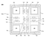
- the first constraining thin film 14 of the resin layer 4 disposed on the opposite side of the resin layer 3 from the substrate 1, and the respective thin film resistance elements R1, R2 (resistance thin film 12) are arranged so as to overlap with each other in plan view, and the second restraining thin film 11 of the resin layer 2 disposed on the substrate 1 side of the resin layer 3 and the thin film resistor elements R1 and R2 (resistive thin film 12) are planar. They are arranged so as to overlap with each other.
- the first and second constraining thin films 11 and 14 are formed so as to overlap with each of the resistive thin films 12 in plan view, but individually overlap with each of the resistive thin films 12 in plan view, or Each of the first and second constraining thin films 11 and 14 may be separately formed into a plurality so as to overlap each other in a plan view for each group of the plurality of resistance thin films 12.
- a plurality of Au / Ni external electrodes 15 are formed on the extraction electrode 13 and are formed of resin so as to cover the extraction electrode 13 and the first constraining thin film 14 and the edge portions of each external electrode 15.
- the protective layer 16 is laminated on the one main surface 4 a of the resin layer 4.
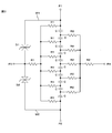
- Each of the ESD protection elements D1, D2 is formed of a bidirectional Zener diode as shown in FIG.
- the method of forming the bidirectional Zener diode is not particularly limited and is not shown in the figure.
- the first semiconductor thin film of one of the p-type and n-type conductivity and the other conductivity type may be used.
- a semiconductor film formed by n-type a-Si on a substrate 1 made of pn junction with a second semiconductor thin film or, for example, B-doped Si-formed p-type Thus, the ESD protection elements D1 and D2 can be formed.
- the thin film device 100 configured as described above includes first to fourth external electrodes P1 to P4 each formed by an external electrode 15, and includes first and second external electrodes P1, Ten thin film capacitor elements C are connected in series between P2.
- the other end of one of the plurality of first thin film resistance elements R1 having one end connected to the third external electrode P3 and the second thin film resistance element R2 having one end connected to the fourth external electrode P4.
- the other end of each of the first thin film resistor elements R1 and each of the second thin films so that any one of the plurality of thin film capacitor elements C is inserted between the other end of each of the first thin film resistor elements C1.
- the other end of each resistance element R2 is connected to both ends of each thin film capacitor element C.
- ESD electrostatic discharge
- a lower capacitor electrode layer 5, a dielectric layer 6, and an upper capacitor electrode layer 7 are formed in a predetermined region on a substrate 1 made of, for example, Si to form a plurality of thin film capacitor elements C.
- a protective layer 8 covering the capacitor element C is formed.
- a resin layer 2 made of a polybenzoxazole-based photosensitive resin insulating film having through holes formed by photolithography is formed, and a heat treatment for curing the resin layer is performed.
- the SiO 2 moisture-resistant protective film in the through holes of the resin layer 2 is removed by dry etching, and a Ti film for forming the extraction electrodes 9 and 10 and the second constraining thin film 11 is formed by sputtering. Then, a Cu film is formed. Then, a pattern is formed by etching by photolithography, and the extraction electrodes 9 and 10 and the second constraining thin film 11 are formed. Next, a resin layer 3 made of a phenol-based photosensitive resin insulating film having through holes formed by photolithography is formed, and a heat treatment for curing the resin layer is performed.
- a lift-off resist is formed, and a resistance thin film 12 is formed by vapor deposition by a lift-off method using a vapor deposition material made of a mixture mainly composed of Ni, Cr, and Si.
- each resistive thin film 12 is disposed so as to overlap the second constraining thin film 11 in plan view.
- a part or all of the plurality of resistance thin films 12 may be arranged so as to overlap with the extraction electrodes 9 and 10 in a plan view instead of the second constraining thin film 11.
- a resin layer 4 made of a phenol-based photosensitive resin insulating film having through holes formed by photolithography is formed, and a heat treatment for curing the resin layer is performed.
- a Ti film for forming the extraction electrode 13 and the first constraining thin film 14 is formed, and a Cu film is formed.
- a resist having openings provided at predetermined positions is patterned on the formed Cu / Ti film, and the external electrodes 15 constituting the first to fourth external electrodes P1 to P4 are formed by Cu / Ti film by plating. It is formed at a predetermined position above. Then, after the resist is removed, the Cu / Ti film is patterned by photolithography etching to form the extraction electrode 15 and the first constraining thin film 14. At this time, the first constraining thin film 14 is disposed so as to overlap each of the resistive thin films 12 in plan view. A part of the plurality of resistive thin films 12 may be arranged so as to overlap with the extraction electrode 13 in plan view instead of the first constraining thin film 14.
- each thin film device 100 is subjected to dicing by dicing.
- the thin film device 100 is completed by being separated into pieces.
- the thin film device 100 configured as described above is mounted on another wiring board or the like using solder, wire bonding, or the like, so that the variable capacitance element having the first and second external electrodes P1 and P2 as input / output terminals is provided. Used as. That is, by adjusting the voltage between the third and fourth external electrodes P3 and P4, the voltage applied to both ends of each thin film capacitor element C through the first and second thin film resistance elements R1 and R2 can be arbitrarily set. By adjusting, the capacitance of each thin film capacitor element C can be adjusted.
- 3 is an example, and the number of variable capacitor elements C, the number of first and second thin film resistance elements R1 and R2, and the number of ESD protection elements D1 and D2 are examples shown in FIG. It is not limited to.
- the resin layer 3 on which the thin film resistance element is formed has a coefficient of thermal expansion. It tries to expand toward the side opposite to the small substrate 1, but the first layer so as to overlap the resin layer 4 disposed on the upper side of the resin layer 3 with the thin film resistance element formed on the resin layer 3 in plan view.
- the constraining thin film 14 is formed.
- the thin film resistor elements R1, R2 are pressed against the substrate 1 by the first constraining thin film 14, and the resin layer 3 expands at a high temperature, whereby the thin film resistor elements R1, R2 (resistance Since the bending stress applied to the thin film 12) can be relaxed, it is possible to prevent the thin film resistor elements R1 and R2 from being damaged by the stress generated by the expansion of the resin layers 2 to 4.
- the thin film resistor elements R1 and R2 are disposed between the substrate 1 and the first constraining thin film 14, the stress generated by the impact when the thin film device 100 is mounted on another substrate or the like is different. Direct application to the thin film resistor elements R1, R2 can be prevented.
- the first constraining thin film 14 is formed to be extended to the edge of the resin layer 3 so as to be exposed on the side surface of the thin film device 100. Therefore, the stress absorbed by the first restraining thin film 14 can be effectively released to the side surface of the thin film device 100.
- the first constraining thin film 14 can be formed on the one main surface 3a of the resin layer 3 by using the same material by the same thin film forming process as that of the extraction electrode 13, the first constraining thin film 14 is formed.
- the process for forming 14 can be simplified. Therefore, it is possible to provide a highly reliable thin film device 100 in which cracking and disconnection of each thin film resistor element R1, R2 (resistive thin film 12) is prevented by using a conventional manufacturing process without increasing the manufacturing process. .
- first constraining thin film 14 and the extraction electrode 13 are formed separately, it is possible to suppress the stress absorbed by the first constraining thin film 14 from being applied to the extraction electrode 13.
- a second restraining thin film 11 is disposed on one main surface 2a of the resin layer 2 disposed on the substrate 1 side with respect to the resin layer 3 so as to overlap the thin film resistor elements R1 and R2 in plan view. Therefore, each thin film resistance element R1, R2 is sandwiched between the first constraining thin film 14 of the resin layer 4 and the second constraining thin film 11 of the resin layer 2. Therefore, the bending stress applied to each thin film resistance element R1, R2 due to expansion of the resin layers 2-4 in a high temperature state can be further alleviated, so that each thin film resistance element is caused by the stress generated by the expansion of the resin layers 2-4. It is possible to more reliably prevent R1 and R2 (resistance thin film 12) from being damaged.
- This embodiment differs from the first embodiment described above in that the first constraining thin film 14 and the extraction electrode 13 are integrally formed as shown in FIGS. Since other configurations are the same as those in the first embodiment, description of the configurations is omitted by citing the same reference numerals.
- the first constraining thin film 14 prevents the first and second thin film resistance elements R1 and R2 from being damaged.
- the highly reliable thin film device 100 can be provided.
- This embodiment is different from the first embodiment described above in that the second constraining thin film 11 is not provided as shown in FIG.
- differences from the above-described first embodiment will be mainly described, and other configurations are the same as those of the above-described first embodiment. Therefore, the same reference numerals are used to describe the configuration. Is omitted.
- the thin film device 100 a includes a substrate 1, a plurality of resin layers 3 and 4 stacked on the one main surface 1 a side of the substrate 1, and a thin film resistance element R.
- the thin film resistance element R is formed by a resistance thin film 12 mainly composed of Ni, Cr, and Si formed by a thin film formation process in a predetermined region of the one main surface 3a of the resin layer 3 laminated on the one main surface 1a of the substrate 1. It is formed.
- the thin film resistive element R resistive thin film 12
- the thin film resistive element R is covered with a resin layer 4 laminated on one main surface 3a of the resin layer 3.
- a Cu / Ti extraction electrode 13 electrically connected to the thin film resistance element R through a through hole (not shown) formed in the resin layer 4, and a first The constraining thin film 14 is formed.
- the first constraining thin film 14 and the thin film resistance element R are arranged so as to overlap in plan view. Further, in this embodiment, the first constraining thin film 14 and the extraction electrode 13 are integrally formed, but the first constraining thin film 14 and the extraction electrode 13 may be formed separately.
- a plurality of Au / Ni external electrodes 15 are formed on the extraction electrode 13 and are formed of resin so as to cover the extraction electrode 13 and the first constraining thin film 14 and the edge portions of each external electrode 15.
- the protective layer 16 is laminated on the one main surface 4 a of the resin layer 4.
- a resin layer 3 made of a polybenzoxazole-based photosensitive resin insulating film is formed on a substrate 1 made of, for example, Si, and a heat treatment for curing the resin layer is performed.
- a lift-off resist is formed, and the resistive thin film 12 is formed by vapor deposition by a lift-off method using a vapor deposition material made of a mixture containing Ni, Cr, and Si as main components.
- a resin layer 4 made of a phenol-based photosensitive resin insulating film in which through holes (not shown) are formed by photolithography is formed, and heat treatment for curing the resin layer is performed.
- a Ti film for forming the extraction electrode 13 and the first constraining thin film 14 is formed, and a Cu film is formed.
- a resist having an opening provided at a predetermined position is patterned on the formed Cu / Ti film, and the external electrode 15 is formed at a predetermined position on the Cu / Ti film by plating.
- the Cu / Ti film is patterned by photolithography etching to form the extraction electrode 15 and the first constraining thin film 14.
- the first constraining thin film 14 is disposed so as to overlap each of the resistive thin films 12 in plan view.
- a part of the plurality of resistive thin films 12 may be arranged so as to overlap with the extraction electrode 13 in plan view instead of the first constraining thin film 14.
- a protective layer 16 made of a phenol-based photosensitive resin insulating film having external electrode exposed portions formed by photolithography is formed, and after heat treatment for curing the resin layer, dicing is performed for each thin film device 100a.
- the thin film device 100a is completed by being separated into pieces.
- the thin film resistance element R is pressed against the substrate 1 by the first constraining thin film 14, and the resin is, for example, in a high temperature state. Even if the layer 3 expands, the bending stress applied to the thin film resistive element R (resistive thin film 12) can be relaxed, so that the thin film resistive element R is damaged by the stress generated by the expansion of the resin layers 3 and 4. Can be prevented.
- the present invention is not limited to the above-described embodiment, and various modifications other than those described above can be made without departing from the spirit of the present invention. They may be combined.
- the material of the thin film resistance elements R, R1, R2 (resistance thin film 12) is not limited to the above-described example, and the thin film resistance elements R, R1, R2 may be formed of, for example, a CrSi alloy.
- the thin film resistor elements R, R1, and R2 may be formed of a conductive material such as Pt.
- first constraining thin film 14 and / or the second constraining thin film 11 are arranged so as to cover (overlap) the entire thin film resistor elements R, R1, R2 (resistive thin film 12) in plan view. It is good to be. In this way, when the resin layers 2 to 4 expand, stress can be uniformly applied to the entire resistance thin film 12 with respect to the thin film resistance elements R, R1, and R2. It is possible to further reliably prevent bending stress from being applied to the (thin film resistance elements R, R1, R2), and to more reliably prevent the thin film resistance elements R, R1, R2 from being damaged.
- a thin film device in which various circuits including the thin film resistor element are configured by appropriately combining thin film circuit elements such as a thin film capacitor element, a thin film inductor element, and a thin film thermistor element is provided.
- the thin film capacitor element, the thin film inductor element, and the thin film thermistor element may have a general thin film circuit element structure.
- a device for adjusting antenna sensitivity of a short-range communication device or a noise filter device for photodiodes can be constituted by the thin film device of the present invention.
- the dielectric material for forming the dielectric layer is not limited to the above example.
- the dielectric layer may be formed of a dielectric material such as BaTiO 3 , SrTiO 3 , or PbTiO 3 .
- the present invention can be widely applied to a thin film device including a thin film resistance element.
Landscapes
- Semiconductor Integrated Circuits (AREA)
- Non-Adjustable Resistors (AREA)
- Engineering & Computer Science (AREA)
- Power Engineering (AREA)
- Parts Printed On Printed Circuit Boards (AREA)
Abstract
樹脂層が膨張することにより生じる応力により薄膜抵抗素子が破損するのを防止して、信頼性の高い薄膜デバイスを得ることができる技術を提供することを目的とする。 樹脂層3の基板1と反対側に配置された樹脂層4に薄膜抵抗素子(抵抗薄膜12)と平面視で重なるように形成された第1の拘束用薄膜14により、薄膜抵抗素子を基板1に対し押さえ込むことができるので、高温状態において樹脂層2~4が膨張することにより薄膜抵抗素子に加わる曲げ応力を緩和することができ、樹脂層2~4の膨張により生じる応力によって薄膜抵抗素子が破損するのを防止することができる。
Description
本発明は、薄膜抵抗素子を備える薄膜デバイスに関する。
従来、薄膜抵抗素子を備える種々の薄膜デバイスが提供されている(例えば特許文献1参照)。例えば、図7に示す従来の薄膜デバイス500は、半導体基板501上に形成された集積回路502と、集積回路502上に配置された複数の電極パッド503と、各電極パッド503間に設けられたパッシベーション膜504上に形成された樹脂層505とを備えている。また、樹脂層505はポリイミド樹脂やエポキシ樹脂等により形成され、樹脂層505の電極パッド503に重なる位置に貫通孔が設けられている。また、貫通孔内においてバリアメタル層506を介して電極パッド503に接続される再配線507が樹脂層505上に形成されている。そして、樹脂層505上の再配線507に挟まれた位置に薄膜抵抗素子508が設けられている。
図7に示す薄膜デバイス500では、薄膜抵抗素子508は、バリアメタル層506と、バリアメタル層506上に積層されたシード層509とを備えている。バリアメタル層506は、Ti、TiN、Ni等により形成され、電極パッド503と再配線507との密着性を向上させるために設けられている。また、シード層509は、再配線507をめっき法により形成する際の電極として機能するものであり、Cu、Al等により形成されている。そして、バリアメタル層506およびシード層509それぞれの膜厚が適宜調整されることにより、薄膜抵抗素子508の抵抗値が調整されている。
ところで、図7に示す薄膜デバイス500が、他の基板などに実装等される際の熱サイクルにおいて加熱された場合に、樹脂層505が膨張すること等により薄膜抵抗素子508に曲げ応力が加わり、薄膜抵抗素子508が破損するおそれがある。
この発明は、上記した課題に鑑みてなされたものであり、樹脂層が膨張することにより生じる応力等により薄膜抵抗素子が破損するのを防止して、信頼性の高い薄膜デバイスを得ることができる技術を提供することを目的とする。
上記した目的を達成するために、本発明の薄膜デバイスは、基板と、前記基板の一方主面側に積層された複数の樹脂層と、を備え、前記複数の樹脂層は、薄膜形成プロセスによって形成された薄膜抵抗素子が一方主面に設けられた第1の樹脂層と、前記第1の樹脂層の前記基板と反対側に配置され、薄膜形成プロセスにより形成された第1の拘束用薄膜が一方主面に設けられた第2の樹脂層とを含み、前記薄膜抵抗素子と前記第1の拘束用薄膜とが平面視で重なるように配置されている、ことを特徴としている。
このように構成された発明では、他の基板などに実装等される際の熱サイクルにおいて薄膜デバイスが加熱された場合に、薄膜抵抗素子が形成された第1の樹脂層は、熱膨張率が小さい基板と反対側に向って膨張しようとするが、第1の樹脂層の基板と反対側に配置された第2の樹脂層に、第1の樹脂層に形成された薄膜抵抗素子と平面視で重なるように第1の拘束用薄膜が形成されている。したがって、薄膜抵抗素子が第1の拘束用薄膜により基板に対して押さえ込まれた状態になり、高温状態において樹脂層が膨張することにより薄膜抵抗素子に加わる曲げ応力を緩和することができるので、樹脂層が膨張することにより生じる応力により薄膜抵抗素子が破損するのを防止することができる。
また、前記第2の樹脂層の一方主面に、薄膜形成プロセスにより形成されて前記薄膜抵抗素子に電気的に接続された配線用薄膜電極が形成されていてもよい。
このようにすると、第1の拘束用薄膜を、配線用薄膜電極と同一の薄膜形成プロセスにより同一の材料を用いて形成することができるので、第1の拘束用薄膜を形成するための工程を簡略化することができ、製造工程を増大させることなく従来の製造工程を用いて、薄膜抵抗素子のクラックや断線が防止された信頼性の高い薄膜デバイスを提供することができる。
また、前記第1の拘束用薄膜と前記配線用薄膜電極とが分離して形成されているとよい。
このようにすると、第1の拘束用薄膜により吸収された応力が配線用薄膜電極に加わるのを抑制することができる。
また、前記第1の拘束用薄膜と前記配線用薄膜電極とが一体形成されていてもよい。
このようにしても、第1の拘束用薄膜により薄膜抵抗素子が破損するのが防止された信頼性の高い薄膜デバイスを提供することができる。
また、前記複数の樹脂層は、前記第1の樹脂層の前記基板側に配置され、薄膜形成プロセスにより形成された第2の拘束用薄膜が一方主面に設けられた第3の樹脂層をさらに含み、前記薄膜抵抗素子と前記第2の拘束用薄膜とが平面視で重なるように配置されているとよい。
このように構成すると、薄膜抵抗素子が、第2の樹脂層の第1の拘束用薄膜と第3の樹脂層の第2の拘束用薄膜の間に挟み込まれた状態となり、高温状態において樹脂層が膨張することにより薄膜抵抗素子に加わる曲げ応力をさらに緩和することができるので、樹脂層が膨張することにより生じる応力により薄膜抵抗素子が破損するのをさらに確実に防止することができる。
また、前記薄膜抵抗素子は、Siを含有していてもよい。
このようにしても、Siを含有することにより脆くなった薄膜抵抗素子の破損を防止した信頼性の高い薄膜デバイスを提供することができる。
また、第1~第4外部電極と、前記第1、第2外部電極間に直列接続された可変容量型の薄膜キャパシタ素子と、一端が前記第3外部電極に接続された第1の前記薄膜抵抗素子と、一端が前記第4外部電極に接続された第2の前記薄膜抵抗素子と、を備え、前記第1、第2の薄膜抵抗素子の他端間に前記薄膜キャパシタ素子が挿入されるように、前記第1、第2の薄膜抵抗素子それぞれの他端が前記薄膜キャパシタ素子両端のそれぞれに接続されているとよい。
このように構成すると、第1、第2外部電極を入出力端子とする可変容量型の薄膜キャパシタ素子を備える薄膜デバイスを提供することができる。すなわち、第3、第4外部電極間の電圧を調整して第1、第2の薄膜抵抗素子を介して薄膜キャパシタ素子の両端に印加される電圧を任意に調整することにより薄膜キャパシタ素子の容量を調整することができる。
また、所定電圧以上の静電気放電が生じた場合に前記第1、第2の薄膜抵抗素子および前記薄膜キャパシタ素子を経由しない電流パスを形成するESD保護素子をさらに備えていてもよい。
このように構成すると、所定電圧以上の静電気放電(ESD:Electro-Static Discharge)に起因する過電圧が生じると、第1、第2の薄膜抵抗素子および薄膜キャパシタ素子を経由しない電流パスがESD保護素子により形成されるので、第1、第2の薄膜抵抗素子および薄膜キャパシタ素子を過電圧から保護することができる。
本発明によれば、第1の樹脂層の基板と反対側に配置された第2の樹脂層に薄膜抵抗素子と平面視で重なるように形成された第1の拘束用薄膜により、薄膜抵抗素子を基板に対し押さえ込むことができるので、高温状態において樹脂層が膨張することにより薄膜抵抗素子に加わる曲げ応力等を緩和することができ、樹脂層が膨張することにより生じる応力等によって薄膜抵抗素子が破損するのを防止し、信頼性の高い薄膜抵抗素子付きの薄膜デバイスを得ることができる。
<第1実施形態>
本発明の第1実施形態について図1~図3を参照して説明する。なお、図1および図2では、説明を簡易なものとするために本発明にかかる主要な構成のみが図示されている。また、後の説明で参照する図4~図6についても、図1および図2と同様に主要な構成のみが図示されているが、以下の説明においてはその説明は省略する。
本発明の第1実施形態について図1~図3を参照して説明する。なお、図1および図2では、説明を簡易なものとするために本発明にかかる主要な構成のみが図示されている。また、後の説明で参照する図4~図6についても、図1および図2と同様に主要な構成のみが図示されているが、以下の説明においてはその説明は省略する。
(構成)
薄膜デバイス100の概略構成について説明する。
薄膜デバイス100の概略構成について説明する。
薄膜デバイス100は、ガラス基板やセラミック基板、樹脂基板、Si基板(Siの線膨張係数:3.4×10⁻⁶/K)、GaAs基板などの基板1と、基板1の一方主面1a側に積層された複数の樹脂層2,3,4と、基板1の一方主面1a上に設けられた可変容量型の複数(この実施形態では10個)の薄膜キャパシタ素子Cと、複数(この実施形態では7個)の第1の薄膜抵抗素子R1(本発明の「薄膜抵抗素子」に相当)と、複数(この実施形態では6個)の第2の薄膜抵抗素子R2(本発明の「薄膜抵抗素子」に相当)と、複数(この実施形態では2個)のESD保護素子D1,D2とを備えている。
薄膜キャパシタ素子Cは、基板1の一方主面1a上の所定領域にPt薄膜により形成されたキャパシタ電極層5と、(Ba,Sr)TiO3(以下「BST」と称する)誘電体層6と、BST誘電体層6上にPt薄膜により形成されたキャパシタ電極層7とにより形成される。
また、薄膜キャパシタ素子Cは、SiO2耐湿保護膜により形成された保護層8により被覆され、保護層8上に樹脂層2が積層されている。樹脂層2(本発明の「第3の樹脂層」に相当)の一方主面2aには、保護層8および樹脂層2に形成された透孔を介して薄膜キャパシタ素子Cの上側のキャパシタ電極層7に接続されたCu/Ti引出電極9と、薄膜キャパシタ素子Cの下側のキャパシタ電極層5に接続されたCu/Ti引出電極10と、第2の拘束用薄膜11とが形成されている。
第2の拘束用薄膜11は、同一の薄膜形成プロセスにより同一の材質を用いて引出電極9,10と同時に形成されている。また、樹脂層2に、引出電極9,10および第2の拘束用薄膜11を被覆して樹脂層3が積層されている。なお、この実施形態では、第2の拘束用薄膜11と引出電極10とが一体形成されているが、第2の拘束用薄膜11と引出電極10とが分離して形成されていてもよいし、第2の拘束用薄膜11が樹脂層2の一方主面2aに形成された他の引出電極と一体的に形成されていてもよい。
各薄膜抵抗素子R1,R2は、それぞれ、樹脂層3(本発明の「第1の樹脂層」に相当)(樹脂層3の線膨張係数:54.0×10⁻⁶/K)の一方主面3aの所定領域に薄膜形成プロセスにより形成されたNi、Cr、Siを主成分とする抵抗薄膜12により形成される。なお、この実施形態では、各薄膜抵抗素子R1,R2の全てが樹脂層3上に形成されているが、各薄膜抵抗素子R1,R2が、それぞれ、異なる樹脂層上に分散して配置されていてもよい。
また、各薄膜抵抗素子R1,R2(抵抗薄膜12)は、樹脂層3の一方主面3a上に積層された樹脂層4により被覆されている。また、樹脂層4(本発明の「第2の樹脂層」に相当)(樹脂層4の線膨張係数:54.0×10⁻⁶/K)の一方主面4aには、樹脂層3,4に形成された透孔を介して引出電極9,10や薄膜抵抗素子R1~R13に電気的に接続されたCu/Ti引出電極13(本発明の「配線用薄膜電極」に相当)(Cuの線膨張係数:16.5×10-6/K、Tiの線膨張係数:8.6×10-6/K)と、第1の拘束用薄膜14とが形成されている。第1の拘束用薄膜14は、同一の薄膜形成プロセスにより同一の材質を用いて引出電極13と同時に形成されている。また、第1の拘束用薄膜14と引出電極13とは分離して形成されている。
また、図1および図2に示すように、樹脂層3の基板1と反対側に配置された樹脂層4の第1の拘束用薄膜14と、各薄膜抵抗素子R1,R2(抵抗薄膜12)とが平面視で重なるように配置され、樹脂層3の基板1側に配置された樹脂層2の第2の拘束用薄膜11と、各薄膜抵抗素子R1,R2(抵抗薄膜12)とが平面視で重なるように配置されている。なお、各抵抗薄膜12の全てと平面視で重なるように第1、第2の拘束用薄膜11,14が形成されているが、各抵抗薄膜12それぞれと個別に平面視で重なるように、もしくは、複数個の抵抗薄膜12のグループごとに平面視で重なるように、第1、第2の拘束用薄膜11,14それぞれが複数個に分離して形成されていてもよい。
また、引出電極13上に複数のAu/Ni外部電極15が形成され、引出電極13および第1の拘束用薄膜14と、各外部電極15それぞれの端縁部分とを被覆するように樹脂により形成された保護層16が樹脂層4の一方主面4a上に積層されている。
ESD保護素子D1,D2それぞれは、図3に示すように、双方向ツェナーダイオードにより形成されている。双方向ツェナーダイオードの形成方法については特に限定されるものではなく、図示省略されているが、例えば、p型およびn型のいずれか一方の導電型の第1の半導体薄膜と他方の導電型の第2の半導体薄膜とがpn接合されて形成されたものや、例えば、Bドープされてp型に形成されたSiから成る基板1上にn型a-Siにより半導体膜が成膜されて形成されたものにより、ESD保護素子D1,D2を形成することができる。
以上のように構成された薄膜デバイス100は、図3に示すように、それぞれ外部電極15により形成された第1~第4外部電極P1~P4を有し、第1、第2外部電極P1,P2間に10個の薄膜キャパシタ素子Cが直列接続されている。また、一端が第3外部電極P3に接続された複数の第1の薄膜抵抗素子R1のうちのいずれかの他端と、一端が第4外部電極P4に接続された第2の薄膜抵抗素子R2のうちのいずれかの他端との間に複数の薄膜キャパシタ素子Cのうちのいずれか1個が挿入されるように、各第1の薄膜抵抗素子R1それぞれの他端および各第2の薄膜抵抗素子R2それぞれの他端が各薄膜キャパシタ素子Cそれぞれの両端に接続されている。
また、所定電圧以上の静電気放電(ESD:Electro-Static Discharge)が生じた場合に、第1、第2の薄膜抵抗素子R1,R2および薄膜キャパシタ素子Cを経由しない電流パスW1,W2が形成されるように、第1、第3外部電極P1,P3間にESD保護素子D1が直列接続され、第2、第3外部電極P2,P3間にESD保護素子D2が直列接続されている。
したがって、所定電圧以上の静電気放電に起因する過電圧が生じると、第1、第2の薄膜抵抗素子R1,R2および薄膜キャパシタ素子Cを経由しない電流パスW1,W2がESD保護素子D1,D2により形成されるので、第1、第2の薄膜抵抗素子R1,R2および薄膜キャパシタ素子Cを過電圧から保護することができる。
(製造方法)
薄膜デバイス100の製造方法の一例について説明する。なお、この実施形態では、大面積の基板1が用いられて複数の薄膜デバイス100の集合体が形成された後に個片化されることにより、複数の薄膜デバイス100が同時に形成される。なお、以下の説明においては、ESD保護素子D1,D2の形成方法の説明は省略する。
薄膜デバイス100の製造方法の一例について説明する。なお、この実施形態では、大面積の基板1が用いられて複数の薄膜デバイス100の集合体が形成された後に個片化されることにより、複数の薄膜デバイス100が同時に形成される。なお、以下の説明においては、ESD保護素子D1,D2の形成方法の説明は省略する。
まず、例えばSiにより形成された基板1上の所定領域に下側のキャパシタ電極層5、誘電体層6、上側のキャパシタ電極層7が形成されて複数の薄膜キャパシタ素子Cが形成され、各薄膜キャパシタ素子Cを被覆する保護層8が形成される。次に、フォトリソグラフィによって透孔が形成されたポリベンゾオキサゾール系感光性樹脂絶縁膜から成る樹脂層2が形成され、樹脂層硬化のための熱処理が行われる。
続いて、樹脂層2の透孔内のSiO2耐湿保護膜をドライエッチングにより除去し、スパッタ法を用いて、引出電極9,10および第2の拘束用薄膜11を形成するTi膜が成膜され、Cu膜が成膜される。そして、フォトリソグラフィによるエッチングによりパターン形成されて、引出電極9,10および第2の拘束用薄膜11が形成される。次に、フォトリソグラフィによって透孔が形成されたフェノール系感光性樹脂絶縁膜から成る樹脂層3が形成され、樹脂層硬化のための熱処理が行われる。
次に、リフトオフレジストが形成され、Ni、Cr、Siを主成分とする混合物から成る蒸着材料を用いて、リフトオフ法により抵抗薄膜12が蒸着形成される。このとき、各抵抗薄膜12は、それぞれ、第2の拘束用薄膜11に平面視で重なるように配置される。なお、複数の抵抗薄膜12のうちの一部または全てが、第2の拘束用薄膜11の代わりに、引出電極9,10と平面視で重なるように配置されていてもよい。
続いて、フォトリソグラフィによって透孔が形成されたフェノール系感光性樹脂絶縁膜から成る樹脂層4が形成され、樹脂層硬化のための熱処理が行われる。そして、スパッタ法を用いて、引出電極13および第1の拘束用薄膜14を形成するTi膜が成膜され、Cu膜が成膜される。
次に、形成されたCu/Ti膜上に所定位置に開口が設けられたレジストがパターン形成されて、めっき法により第1~第4外部電極P1~P4を成す外部電極15がCu/Ti膜上の所定位置に形成される。そして、レジストが除去された後に、フォトリソグラフィによるエッチングによりCu/Ti膜がパターン形成されて、引出電極15および第1の拘束用薄膜14が形成される。このとき、第1の拘束用薄膜14は、各抵抗薄膜12それぞれと平面視で重なるように配置される。なお、複数の抵抗薄膜12のうちの一部が、第1の拘束用薄膜14の代わりに、引出電極13と平面視で重なるように配置されていてもよい。
そして、フォトリソグラフィによって外部電極露出部が形成されたフェノール系感光性樹脂絶縁膜からなる保護層16が形成され、樹脂層硬化のための熱処理が行われた後に、ダイシングにより各薄膜デバイス100ごとに個片化されることによって、薄膜デバイス100が完成する。
このように構成された薄膜デバイス100は、他の配線基板等にはんだやワイヤボンディング等を用いて実装されることにより、第1、第2外部電極P1,P2を入出力端子とする可変容量素子として使用される。すなわち、第3、第4外部電極P3,P4間の電圧を調整して第1、第2の薄膜抵抗素子R1,R2を介して各薄膜キャパシタ素子Cそれぞれの両端に印加される電圧を任意に調整することにより各薄膜キャパシタ素子Cそれぞれの容量を調整することができる。なお、図3に示す電気回路は一例であって、可変キャパシタ素子Cの数や第1、第2の薄膜抵抗素子R1,R2の数、ESD保護素子D1,D2の数は図3に示す例に限定されるものではない。
以上のように、この実施形態では、他の基板などに実装等される際の熱サイクルにおいて薄膜デバイス100が加熱された場合に、薄膜抵抗素子が形成された樹脂層3は、熱膨張率が小さい基板1と反対側に向って膨張しようとするが、樹脂層3よりも上層側に配置された樹脂層4に、樹脂層3に形成された薄膜抵抗素子と平面視で重なるように第1の拘束用薄膜14が形成されている。したがって、各薄膜抵抗素子R1,R2が第1の拘束用薄膜14により基板1に対して押さえ込まれた状態になり、高温状態において樹脂層3が膨張することにより各薄膜抵抗素子R1,R2(抵抗薄膜12)に加わる曲げ応力を緩和することができるので、各樹脂層2~4が膨張することにより生じる応力により各薄膜抵抗素子R1,R2が破損するのを防止することができる。
また、基板1と第1の拘束用薄膜14との間に各薄膜抵抗素子R1,R2が配置されているので、薄膜デバイス100が他の基板等にマウントされた際の衝撃により生じる応力が各薄膜抵抗素子R1,R2に直接的に加わるのを防止することができる。
また、この実施形態では、図2に示すように、第1の拘束用薄膜14は、薄膜デバイス100の側面に露出するように、樹脂層3の端縁部まで引き伸ばされて形成されている。したがって、第1の拘束用薄膜14により吸収した応力を薄膜デバイス100の側面に効果的に逃がすことができる。
また、第1の拘束用薄膜14を、引出電極13と同一の薄膜形成プロセスにより同一の材料を用いて樹脂層3の一方主面3a上に形成することができるので、第1の拘束用薄膜14を形成するための工程を簡略化することができる。したがって、製造工程を増大させることなく従来の製造工程を用いて、各薄膜抵抗素子R1,R2(抵抗薄膜12)のクラックや断線が防止された信頼性の高い薄膜デバイス100を提供することができる。
また、第1の拘束用薄膜14と引出電極13とが分離して形成されているので、第1の拘束用薄膜14により吸収された応力が引出電極13に加わるのを抑制することができる。
また、樹脂層3よりも基板1側に配置された樹脂層2の一方主面2a上に、各薄膜抵抗素子R1,R2と平面視で重なるように第2の拘束用薄膜11が配置されているので、各薄膜抵抗素子R1,R2が、樹脂層4の第1の拘束用薄膜14と樹脂層2の第2の拘束用薄膜11の間に挟み込まれた状態となる。そのため、高温状態において樹脂層2~4が膨張することにより各薄膜抵抗素子R1,R2に加わる曲げ応力をさらに緩和することができるので、樹脂層2~4の膨張によって生じる応力により各薄膜抵抗素子R1,R2(抵抗薄膜12)が破損するのをさらに確実に防止することができる。
また、上記した構成とすることにより、Siを含有することにより脆くなった各薄膜抵抗素子R1,R2の破損を防止した信頼性の高い薄膜デバイス100を提供することができる。
<第2実施形態>
本発明の第2の実施形態について図4および図5を参照して説明する。
本発明の第2の実施形態について図4および図5を参照して説明する。
この実施形態が上記した第1実施形態と異なるのは、図4および図5に示すように、第1の拘束用薄膜14と引出電極13とが一体形成されている点である。その他の構成は上記した第1実施形態と同様の構成であるため、同一符号を引用することによりその構成の説明は省略する。
このように、第1の拘束用薄膜14と引出電極13とが一体形成されていても、第1の拘束用薄膜14により第1、第2の薄膜抵抗素子R1,R2が破損するのが防止された信頼性の高い薄膜デバイス100を提供することができる。
<第3実施形態>
本発明の第3の実施形態について図6を参照して説明する。
本発明の第3の実施形態について図6を参照して説明する。
この実施形態が上記した第1実施形態と異なるのは、図6に示すように、第2の拘束用薄膜11が設けられていない点である。以下の説明においては、上記した第1実施形態と異なる点を中心に説明し、その他の構成は上記した第1実施形態と同様の構成であるため、同一符号を引用することによりその構成の説明は省略する。
(構成)
薄膜デバイス100aの概略構成について説明する。
薄膜デバイス100aの概略構成について説明する。
薄膜デバイス100aは、基板1と、基板1の一方主面1a側に積層された複数の樹脂層3,4と、薄膜抵抗素子Rとを備えている。
薄膜抵抗素子Rは、基板1の一方主面1aに積層された樹脂層3の一方主面3aの所定領域に薄膜形成プロセスにより形成されたNi、Cr、Siを主成分とする抵抗薄膜12により形成される。そして、薄膜抵抗素子R(抵抗薄膜12)は、樹脂層3の一方主面3a上に積層された樹脂層4により被覆されている。また、樹脂層4の一方主面4aには、樹脂層4に形成された透孔(図示省略)を介して薄膜抵抗素子Rに電気的に接続されたCu/Ti引出電極13と、第1の拘束用薄膜14とが形成されている。なお、上記した第1実施形態と同様に、第1の拘束用薄膜14と、薄膜抵抗素子R(抵抗薄膜12)とが平面視で重なるように配置されている。また、この実施形態では、第1の拘束用薄膜14と引出電極13とが一体形成されているが、第1の拘束用薄膜14と引出電極13とが分離して形成されていてもよい。
また、引出電極13上に複数のAu/Ni外部電極15が形成され、引出電極13および第1の拘束用薄膜14と、各外部電極15それぞれの端縁部分とを被覆するように樹脂により形成された保護層16が樹脂層4の一方主面4a上に積層されている。
(製造方法)
薄膜デバイス100aの製造方法の一例について説明する。なお、上記した第1実施形態と同様に、大面積の基板1が用いられて複数の薄膜デバイス100aの集合体が形成された後に個片化されることにより、複数の薄膜デバイス100aが同時に形成される。
薄膜デバイス100aの製造方法の一例について説明する。なお、上記した第1実施形態と同様に、大面積の基板1が用いられて複数の薄膜デバイス100aの集合体が形成された後に個片化されることにより、複数の薄膜デバイス100aが同時に形成される。
まず、例えばSiにより形成された基板1上にポリベンゾオキサゾール系感光性樹脂絶縁膜から成る樹脂層3が形成され、樹脂層硬化のための熱処理が行われる。次に、リフトオフレジストが形成され、Ni、Cr、Siを主成分とする混合物から成る蒸着材料を用いて、リフトオフ法により抵抗薄膜12が蒸着形成される。続いて、フォトリソグラフィによって透孔(図示省略)が形成されたフェノール系感光性樹脂絶縁膜から成る樹脂層4が形成され、樹脂層硬化のための熱処理が行われる。そして、スパッタ法を用いて、引出電極13および第1の拘束用薄膜14を形成するTi膜が成膜され、Cu膜が成膜される。
次に、形成されたCu/Ti膜上に所定位置に開口が設けられたレジストがパターン形成されて、めっき法により外部電極15がCu/Ti膜上の所定位置に形成される。そして、レジストが除去された後に、フォトリソグラフィによるエッチングによりCu/Ti膜がパターン形成されて、引出電極15および第1の拘束用薄膜14が形成される。このとき、上記した第1実施形態と同様に、第1の拘束用薄膜14は、各抵抗薄膜12それぞれと平面視で重なるように配置される。なお、複数の抵抗薄膜12のうちの一部が、第1の拘束用薄膜14の代わりに、引出電極13と平面視で重なるように配置されていてもよい。
そして、フォトリソグラフィによって外部電極露出部が形成されたフェノール系感光性樹脂絶縁膜からなる保護層16が形成され、樹脂層硬化のための熱処理が行われた後に、ダイシングにより各薄膜デバイス100aごとに個片化されることによって、薄膜デバイス100aが完成する。
以上のように、この実施形態では、上記した第1実施形態と同様に、薄膜抵抗素子Rが第1の拘束用薄膜14により基板1に対して押さえ込まれた状態になり、例えば高温状態において樹脂層3が膨張しても、薄膜抵抗素子R(抵抗薄膜12)に加わる曲げ応力を緩和することができるので、各樹脂層3,4が膨張することにより生じる応力により薄膜抵抗素子Rが破損するのを防止することができる。
なお、本発明は上記した実施形態に限定されるものではなく、その趣旨を逸脱しない限りにおいて、上記したもの以外に種々の変更を行なうことが可能であり、上記した各実施形態がどのように組み合わされてもよい。例えば、薄膜抵抗素子R,R1,R2(抵抗薄膜12)の材質は上記した例に限定されるものではなく、例えばCrSi合金により薄膜抵抗素子R,R1,R2が形成されてもよいし、例えば図7に示す従来の薄膜デバイス500のように、Pt等の導電材料により薄膜抵抗素子R,R1,R2が形成されてもよい。
また、薄膜抵抗素子R,R1,R2(抵抗薄膜12)の全体を平面視で被覆する(重なる)ように、第1の拘束用薄膜14および/または第2の拘束用薄膜11が配置されているとよい。このようにすると、樹脂層2~4が膨張した際に、薄膜抵抗素子R,R1,R2に対して、抵抗薄膜12の全体に応力が均一に加わるようにすることができるため、抵抗薄膜12(薄膜抵抗素子R,R1,R2)に曲げ応力が加わるのをさらに確実に防止することができ、より確実に薄膜抵抗素子R,R1,R2が破損するのを防止することができる。
また、薄膜抵抗素子に追加して、薄膜キャパシタ素子や薄膜インダクタ素子、薄膜サーミスタ素子等の薄膜回路素子が適宜組み合わされることにより、薄膜抵抗素子を備える各種の回路が構成された薄膜デバイスを提供することができる。この場合には、薄膜キャパシタ素子、薄膜インダクタ素子、薄膜サーミスタ素子の構成は、一般的な薄膜回路素子の構成を有していればよい。具体的には、例えば、近距離通信装置のアンテナ感度調整用のデバイスや、フォトダイオード用ノイズフィルタデバイスを本発明の薄膜デバイスにより構成することができる。
また、誘電体層を形成する誘電体材料は上記した例に限定されるものではない。たとえば、BaTiO3、SrTiO3、PbTiO3などの誘電体材料により誘電体層が形成されていてもよい。
薄膜抵抗素子を備える薄膜デバイスに本発明を広く適用することができる。
1 基板
2,3,4 樹脂層
1a,2a,3a,4a 一方主面
11 第2の拘束用薄膜
13 引出電極(配線用薄膜電極)
14 第1の拘束用薄膜
100,100a 薄膜デバイス
C 薄膜キャパシタ素子
D1,D2 ESD保護素子
P1 第1外部電極
P2 第2外部電極
P3 第3外部電極
P4 第4外部電極
R 薄膜抵抗素子
R1 第1の薄膜抵抗素子(薄膜抵抗素子)
R2 第2の薄膜抵抗素子(薄膜抵抗素子)
W1,W2 電流パス
2,3,4 樹脂層
1a,2a,3a,4a 一方主面
11 第2の拘束用薄膜
13 引出電極(配線用薄膜電極)
14 第1の拘束用薄膜
100,100a 薄膜デバイス
C 薄膜キャパシタ素子
D1,D2 ESD保護素子
P1 第1外部電極
P2 第2外部電極
P3 第3外部電極
P4 第4外部電極
R 薄膜抵抗素子
R1 第1の薄膜抵抗素子(薄膜抵抗素子)
R2 第2の薄膜抵抗素子(薄膜抵抗素子)
W1,W2 電流パス
Claims (8)
- 基板と、
前記基板の一方主面側に積層された複数の樹脂層と、を備え、
前記複数の樹脂層は、
薄膜形成プロセスによって形成された薄膜抵抗素子が一方主面に設けられた第1の樹脂層と、
前記第1の樹脂層の前記基板と反対側に配置され、薄膜形成プロセスにより形成された第1の拘束用薄膜が一方主面に設けられた第2の樹脂層とを含み、
前記薄膜抵抗素子と前記第1の拘束用薄膜とが平面視で重なるように配置されている、
ことを特徴とする薄膜デバイス。 - 前記第2の樹脂層の一方主面に、薄膜形成プロセスにより形成されて前記薄膜抵抗素子に電気的に接続された配線用薄膜電極が形成されている、ことを特徴とする請求項1に記載の薄膜デバイス。
- 前記第1の拘束用薄膜と前記配線用薄膜電極とが分離して形成されている、ことを特徴とする請求項1または2に記載の薄膜デバイス。
- 前記第1の拘束用薄膜と前記配線用薄膜電極とが一体形成されている、ことを特徴とする請求項1または2に記載の薄膜デバイス。
- 前記複数の樹脂層は、
前記第1の樹脂層の前記基板側に配置され、薄膜形成プロセスにより形成された第2の拘束用薄膜が一方主面に設けられた第3の樹脂層をさらに含み、
前記薄膜抵抗素子と前記第2の拘束用薄膜とが平面視で重なるように配置されている、
ことを特徴とする請求項1ないし4のいずれかに記載の薄膜デバイス。 - 前記薄膜抵抗素子は、Siを含有する、ことを特徴とする請求項1ないし5のいずれかに記載の薄膜デバイス。
- 第1~第4外部電極と、
前記第1、第2外部電極間に直列接続された可変容量型の薄膜キャパシタ素子と、
一端が前記第3外部電極に接続された第1の前記薄膜抵抗素子と、
一端が前記第4外部電極に接続された第2の前記薄膜抵抗素子と、を備え、
前記第1、第2の薄膜抵抗素子の他端間に前記薄膜キャパシタ素子が挿入されるように、前記第1、第2の薄膜抵抗素子それぞれの他端が前記薄膜キャパシタ素子両端のそれぞれに接続されている、
ことを特徴とする請求項1ないし6いずれかに記載の薄膜デバイス。 - 所定電圧以上の静電気放電が生じた場合に前記第1、第2の薄膜抵抗素子および前記薄膜キャパシタ素子を経由しない電流パスを形成するESD保護素子をさらに備える、ことを特徴とする請求項7に記載の薄膜デバイス。
Priority Applications (3)
| Application Number | Priority Date | Filing Date | Title |
|---|---|---|---|
| CN201690000491.2U CN207425835U (zh) | 2015-02-12 | 2016-01-08 | 薄膜器件 |
| JP2016574686A JP6319467B2 (ja) | 2015-02-12 | 2016-01-08 | 薄膜デバイス |
| US15/674,660 US10332872B2 (en) | 2015-02-12 | 2017-08-11 | Thin-film device |
Applications Claiming Priority (2)
| Application Number | Priority Date | Filing Date | Title |
|---|---|---|---|
| JP2015024914 | 2015-02-12 | ||
| JP2015-024914 | 2015-11-07 |
Related Child Applications (1)
| Application Number | Title | Priority Date | Filing Date |
|---|---|---|---|
| US15/674,660 Continuation US10332872B2 (en) | 2015-02-12 | 2017-08-11 | Thin-film device |
Publications (1)
| Publication Number | Publication Date |
|---|---|
| WO2016129304A1 true WO2016129304A1 (ja) | 2016-08-18 |
Family
ID=56614581
Family Applications (1)
| Application Number | Title | Priority Date | Filing Date |
|---|---|---|---|
| PCT/JP2016/050477 Ceased WO2016129304A1 (ja) | 2015-02-12 | 2016-01-08 | 薄膜デバイス |
Country Status (4)
| Country | Link |
|---|---|
| US (1) | US10332872B2 (ja) |
| JP (1) | JP6319467B2 (ja) |
| CN (1) | CN207425835U (ja) |
| WO (1) | WO2016129304A1 (ja) |
Cited By (1)
| Publication number | Priority date | Publication date | Assignee | Title |
|---|---|---|---|---|
| JP2020170782A (ja) * | 2019-04-03 | 2020-10-15 | 株式会社村田製作所 | キャパシタ |
Families Citing this family (4)
| Publication number | Priority date | Publication date | Assignee | Title |
|---|---|---|---|---|
| US20190304905A1 (en) * | 2018-03-28 | 2019-10-03 | Qualcomm Incorporated | Co-placement of resistor and other devices to improve area & performance |
| JP7180359B2 (ja) * | 2018-12-19 | 2022-11-30 | 富士電機株式会社 | 抵抗素子 |
| CN115088071A (zh) * | 2020-02-17 | 2022-09-20 | 株式会社村田制作所 | 半导体装置以及模块 |
| FR3123501A1 (fr) * | 2021-05-25 | 2022-12-02 | Stmicroelectronics Sa | Capteur passif de décharges éléctrostatiques et procédé de détection de décharges électrostatiques. |
Citations (4)
| Publication number | Priority date | Publication date | Assignee | Title |
|---|---|---|---|---|
| JP2003243522A (ja) * | 2002-02-20 | 2003-08-29 | Mitsubishi Electric Corp | 抵抗素子を使用した半導体装置 |
| JP2006332428A (ja) * | 2005-05-27 | 2006-12-07 | Seiko Instruments Inc | 半導体集積回路装置 |
| JP2010177506A (ja) * | 2009-01-30 | 2010-08-12 | Nec Corp | 配線基板及びその製造方法 |
| WO2013183472A1 (ja) * | 2012-06-08 | 2013-12-12 | 株式会社村田製作所 | 可変容量素子、高周波デバイスおよび通信装置 |
Family Cites Families (6)
| Publication number | Priority date | Publication date | Assignee | Title |
|---|---|---|---|---|
| US5801065A (en) * | 1994-02-03 | 1998-09-01 | Universal Semiconductor, Inc. | Structure and fabrication of semiconductor device having merged resistive/capacitive plate and/or surface layer that provides ESD protection |
| KR101199664B1 (ko) * | 2004-12-28 | 2012-11-08 | 스미토모 베이클리트 컴퍼니 리미티드 | 벤조옥사졸 수지 전구체, 폴리벤조옥사졸 수지, 수지막 및반도체 장치 |
| JP2009266964A (ja) | 2008-04-23 | 2009-11-12 | Fujikura Ltd | 半導体装置 |
| JP5539624B2 (ja) | 2008-04-28 | 2014-07-02 | ラピスセミコンダクタ株式会社 | 薄膜抵抗素子、及び薄膜抵抗素子の製造方法 |
| GB2511233B (en) | 2011-10-26 | 2015-06-24 | Murata Manufacturing Co | Variable capacitance element for wireless communication systems |
| JP6091855B2 (ja) * | 2012-11-16 | 2017-03-08 | 太陽誘電株式会社 | 可変容量複合部品 |
-
2016
- 2016-01-08 JP JP2016574686A patent/JP6319467B2/ja not_active Expired - Fee Related
- 2016-01-08 CN CN201690000491.2U patent/CN207425835U/zh not_active Expired - Fee Related
- 2016-01-08 WO PCT/JP2016/050477 patent/WO2016129304A1/ja not_active Ceased
-
2017
- 2017-08-11 US US15/674,660 patent/US10332872B2/en active Active
Patent Citations (4)
| Publication number | Priority date | Publication date | Assignee | Title |
|---|---|---|---|---|
| JP2003243522A (ja) * | 2002-02-20 | 2003-08-29 | Mitsubishi Electric Corp | 抵抗素子を使用した半導体装置 |
| JP2006332428A (ja) * | 2005-05-27 | 2006-12-07 | Seiko Instruments Inc | 半導体集積回路装置 |
| JP2010177506A (ja) * | 2009-01-30 | 2010-08-12 | Nec Corp | 配線基板及びその製造方法 |
| WO2013183472A1 (ja) * | 2012-06-08 | 2013-12-12 | 株式会社村田製作所 | 可変容量素子、高周波デバイスおよび通信装置 |
Cited By (2)
| Publication number | Priority date | Publication date | Assignee | Title |
|---|---|---|---|---|
| JP2020170782A (ja) * | 2019-04-03 | 2020-10-15 | 株式会社村田製作所 | キャパシタ |
| JP7318279B2 (ja) | 2019-04-03 | 2023-08-01 | 株式会社村田製作所 | キャパシタ |
Also Published As
| Publication number | Publication date |
|---|---|
| JPWO2016129304A1 (ja) | 2017-09-21 |
| CN207425835U (zh) | 2018-05-29 |
| US20170345815A1 (en) | 2017-11-30 |
| US10332872B2 (en) | 2019-06-25 |
| JP6319467B2 (ja) | 2018-05-09 |
Similar Documents
| Publication | Publication Date | Title |
|---|---|---|
| JP6319467B2 (ja) | 薄膜デバイス | |
| US10153267B2 (en) | ESD-protective-function-equipped composite electronic component | |
| CN205452284U (zh) | Esd保护器件 | |
| US10770451B2 (en) | Thin-film ESD protection device | |
| US10200007B2 (en) | Filter chip | |
| CN109994430A (zh) | 半导体元件 | |
| JP6191804B2 (ja) | 薄膜デバイス | |
| US9728306B2 (en) | Micro-resistance structure with high bending strength, manufacturing method and semi-finished structure thereof | |
| TW201820356A (zh) | 附電容器之半導體裝置 | |
| CN108933087B (zh) | 功率模块 | |
| JP6819894B2 (ja) | 電子部品 | |
| US20150162327A1 (en) | Semiconductor module | |
| US8659118B2 (en) | Semiconductor device comprising a fuse structure and a method for manufacturing such semiconductor device | |
| US10410772B2 (en) | Chip resistor | |
| WO2017124793A1 (zh) | 一种电路保护器件 | |
| US9698092B2 (en) | Electronic device | |
| JP2002110923A (ja) | 半導体集積回路装置及びその製造方法 | |
| US20160064614A1 (en) | Light emitting diode package and manufacturing method thereof | |
| TWI490890B (zh) | 過電流保護元件 | |
| JP2010192499A (ja) | 半導体装置 | |
| JP2019506741A (ja) | Esd保護機能を有するデバイス担体とその製造のための方法 |
Legal Events
| Date | Code | Title | Description |
|---|---|---|---|
| 121 | Ep: the epo has been informed by wipo that ep was designated in this application |
Ref document number: 16748949 Country of ref document: EP Kind code of ref document: A1 |
|
| ENP | Entry into the national phase |
Ref document number: 2016574686 Country of ref document: JP Kind code of ref document: A |
|
| NENP | Non-entry into the national phase |
Ref country code: DE |
|
| 122 | Ep: pct application non-entry in european phase |
Ref document number: 16748949 Country of ref document: EP Kind code of ref document: A1 |