WO2016125881A1 - 半導体装置の製造方法、及びアンダーフィルフィルム - Google Patents
半導体装置の製造方法、及びアンダーフィルフィルム Download PDFInfo
- Publication number
- WO2016125881A1 WO2016125881A1 PCT/JP2016/053462 JP2016053462W WO2016125881A1 WO 2016125881 A1 WO2016125881 A1 WO 2016125881A1 JP 2016053462 W JP2016053462 W JP 2016053462W WO 2016125881 A1 WO2016125881 A1 WO 2016125881A1
- Authority
- WO
- WIPO (PCT)
- Prior art keywords
- underfill film
- melt viscosity
- temperature
- underfill
- epoxy resin
- Prior art date
Links
Images


Classifications
-
- C—CHEMISTRY; METALLURGY
- C09—DYES; PAINTS; POLISHES; NATURAL RESINS; ADHESIVES; COMPOSITIONS NOT OTHERWISE PROVIDED FOR; APPLICATIONS OF MATERIALS NOT OTHERWISE PROVIDED FOR
- C09J—ADHESIVES; NON-MECHANICAL ASPECTS OF ADHESIVE PROCESSES IN GENERAL; ADHESIVE PROCESSES NOT PROVIDED FOR ELSEWHERE; USE OF MATERIALS AS ADHESIVES
- C09J7/00—Adhesives in the form of films or foils
- C09J7/10—Adhesives in the form of films or foils without carriers
-
- C—CHEMISTRY; METALLURGY
- C08—ORGANIC MACROMOLECULAR COMPOUNDS; THEIR PREPARATION OR CHEMICAL WORKING-UP; COMPOSITIONS BASED THEREON
- C08G—MACROMOLECULAR COMPOUNDS OBTAINED OTHERWISE THAN BY REACTIONS ONLY INVOLVING UNSATURATED CARBON-TO-CARBON BONDS
- C08G59/00—Polycondensates containing more than one epoxy group per molecule; Macromolecules obtained by polymerising compounds containing more than one epoxy group per molecule using curing agents or catalysts which react with the epoxy groups
- C08G59/18—Macromolecules obtained by polymerising compounds containing more than one epoxy group per molecule using curing agents or catalysts which react with the epoxy groups ; e.g. general methods of curing
- C08G59/40—Macromolecules obtained by polymerising compounds containing more than one epoxy group per molecule using curing agents or catalysts which react with the epoxy groups ; e.g. general methods of curing characterised by the curing agents used
- C08G59/42—Polycarboxylic acids; Anhydrides, halides or low molecular weight esters thereof
-
- C—CHEMISTRY; METALLURGY
- C09—DYES; PAINTS; POLISHES; NATURAL RESINS; ADHESIVES; COMPOSITIONS NOT OTHERWISE PROVIDED FOR; APPLICATIONS OF MATERIALS NOT OTHERWISE PROVIDED FOR
- C09J—ADHESIVES; NON-MECHANICAL ASPECTS OF ADHESIVE PROCESSES IN GENERAL; ADHESIVE PROCESSES NOT PROVIDED FOR ELSEWHERE; USE OF MATERIALS AS ADHESIVES
- C09J133/00—Adhesives based on homopolymers or copolymers of compounds having one or more unsaturated aliphatic radicals, each having only one carbon-to-carbon double bond, and at least one being terminated by only one carboxyl radical, or of salts, anhydrides, esters, amides, imides, or nitriles thereof; Adhesives based on derivatives of such polymers
- C09J133/04—Homopolymers or copolymers of esters
- C09J133/14—Homopolymers or copolymers of esters of esters containing halogen, nitrogen, sulfur or oxygen atoms in addition to the carboxy oxygen
- C09J133/16—Homopolymers or copolymers of esters containing halogen atoms
-
- C—CHEMISTRY; METALLURGY
- C09—DYES; PAINTS; POLISHES; NATURAL RESINS; ADHESIVES; COMPOSITIONS NOT OTHERWISE PROVIDED FOR; APPLICATIONS OF MATERIALS NOT OTHERWISE PROVIDED FOR
- C09J—ADHESIVES; NON-MECHANICAL ASPECTS OF ADHESIVE PROCESSES IN GENERAL; ADHESIVE PROCESSES NOT PROVIDED FOR ELSEWHERE; USE OF MATERIALS AS ADHESIVES
- C09J163/00—Adhesives based on epoxy resins; Adhesives based on derivatives of epoxy resins
- C09J163/08—Epoxidised polymerised polyenes
-
- H—ELECTRICITY
- H01—ELECTRIC ELEMENTS
- H01L—SEMICONDUCTOR DEVICES NOT COVERED BY CLASS H10
- H01L21/00—Processes or apparatus adapted for the manufacture or treatment of semiconductor or solid state devices or of parts thereof
- H01L21/02—Manufacture or treatment of semiconductor devices or of parts thereof
- H01L21/04—Manufacture or treatment of semiconductor devices or of parts thereof the devices having at least one potential-jump barrier or surface barrier, e.g. PN junction, depletion layer or carrier concentration layer
- H01L21/50—Assembly of semiconductor devices using processes or apparatus not provided for in a single one of the subgroups H01L21/06 - H01L21/326, e.g. sealing of a cap to a base of a container
- H01L21/56—Encapsulations, e.g. encapsulation layers, coatings
- H01L21/563—Encapsulation of active face of flip-chip device, e.g. underfilling or underencapsulation of flip-chip, encapsulation preform on chip or mounting substrate
-
- H—ELECTRICITY
- H01—ELECTRIC ELEMENTS
- H01L—SEMICONDUCTOR DEVICES NOT COVERED BY CLASS H10
- H01L23/00—Details of semiconductor or other solid state devices
- H01L23/28—Encapsulations, e.g. encapsulating layers, coatings, e.g. for protection
- H01L23/29—Encapsulations, e.g. encapsulating layers, coatings, e.g. for protection characterised by the material, e.g. carbon
- H01L23/293—Organic, e.g. plastic
-
- H—ELECTRICITY
- H01—ELECTRIC ELEMENTS
- H01L—SEMICONDUCTOR DEVICES NOT COVERED BY CLASS H10
- H01L23/00—Details of semiconductor or other solid state devices
- H01L23/28—Encapsulations, e.g. encapsulating layers, coatings, e.g. for protection
- H01L23/31—Encapsulations, e.g. encapsulating layers, coatings, e.g. for protection characterised by the arrangement or shape
- H01L23/3157—Partial encapsulation or coating
-
- H—ELECTRICITY
- H01—ELECTRIC ELEMENTS
- H01L—SEMICONDUCTOR DEVICES NOT COVERED BY CLASS H10
- H01L24/00—Arrangements for connecting or disconnecting semiconductor or solid-state bodies; Methods or apparatus related thereto
- H01L24/01—Means for bonding being attached to, or being formed on, the surface to be connected, e.g. chip-to-package, die-attach, "first-level" interconnects; Manufacturing methods related thereto
- H01L24/10—Bump connectors ; Manufacturing methods related thereto
- H01L24/12—Structure, shape, material or disposition of the bump connectors prior to the connecting process
- H01L24/13—Structure, shape, material or disposition of the bump connectors prior to the connecting process of an individual bump connector
-
- H—ELECTRICITY
- H01—ELECTRIC ELEMENTS
- H01L—SEMICONDUCTOR DEVICES NOT COVERED BY CLASS H10
- H01L24/00—Arrangements for connecting or disconnecting semiconductor or solid-state bodies; Methods or apparatus related thereto
- H01L24/01—Means for bonding being attached to, or being formed on, the surface to be connected, e.g. chip-to-package, die-attach, "first-level" interconnects; Manufacturing methods related thereto
- H01L24/10—Bump connectors ; Manufacturing methods related thereto
- H01L24/15—Structure, shape, material or disposition of the bump connectors after the connecting process
- H01L24/16—Structure, shape, material or disposition of the bump connectors after the connecting process of an individual bump connector
-
- H—ELECTRICITY
- H01—ELECTRIC ELEMENTS
- H01L—SEMICONDUCTOR DEVICES NOT COVERED BY CLASS H10
- H01L24/00—Arrangements for connecting or disconnecting semiconductor or solid-state bodies; Methods or apparatus related thereto
- H01L24/01—Means for bonding being attached to, or being formed on, the surface to be connected, e.g. chip-to-package, die-attach, "first-level" interconnects; Manufacturing methods related thereto
- H01L24/26—Layer connectors, e.g. plate connectors, solder or adhesive layers; Manufacturing methods related thereto
- H01L24/28—Structure, shape, material or disposition of the layer connectors prior to the connecting process
- H01L24/29—Structure, shape, material or disposition of the layer connectors prior to the connecting process of an individual layer connector
-
- H—ELECTRICITY
- H01—ELECTRIC ELEMENTS
- H01L—SEMICONDUCTOR DEVICES NOT COVERED BY CLASS H10
- H01L24/00—Arrangements for connecting or disconnecting semiconductor or solid-state bodies; Methods or apparatus related thereto
- H01L24/74—Apparatus for manufacturing arrangements for connecting or disconnecting semiconductor or solid-state bodies
- H01L24/75—Apparatus for connecting with bump connectors or layer connectors
-
- H—ELECTRICITY
- H01—ELECTRIC ELEMENTS
- H01L—SEMICONDUCTOR DEVICES NOT COVERED BY CLASS H10
- H01L24/00—Arrangements for connecting or disconnecting semiconductor or solid-state bodies; Methods or apparatus related thereto
- H01L24/80—Methods for connecting semiconductor or other solid state bodies using means for bonding being attached to, or being formed on, the surface to be connected
- H01L24/81—Methods for connecting semiconductor or other solid state bodies using means for bonding being attached to, or being formed on, the surface to be connected using a bump connector
-
- H—ELECTRICITY
- H01—ELECTRIC ELEMENTS
- H01L—SEMICONDUCTOR DEVICES NOT COVERED BY CLASS H10
- H01L24/00—Arrangements for connecting or disconnecting semiconductor or solid-state bodies; Methods or apparatus related thereto
- H01L24/80—Methods for connecting semiconductor or other solid state bodies using means for bonding being attached to, or being formed on, the surface to be connected
- H01L24/83—Methods for connecting semiconductor or other solid state bodies using means for bonding being attached to, or being formed on, the surface to be connected using a layer connector
-
- H—ELECTRICITY
- H01—ELECTRIC ELEMENTS
- H01L—SEMICONDUCTOR DEVICES NOT COVERED BY CLASS H10
- H01L24/00—Arrangements for connecting or disconnecting semiconductor or solid-state bodies; Methods or apparatus related thereto
- H01L24/91—Methods for connecting semiconductor or solid state bodies including different methods provided for in two or more of groups H01L24/80 - H01L24/90
- H01L24/92—Specific sequence of method steps
-
- H—ELECTRICITY
- H01—ELECTRIC ELEMENTS
- H01L—SEMICONDUCTOR DEVICES NOT COVERED BY CLASS H10
- H01L24/00—Arrangements for connecting or disconnecting semiconductor or solid-state bodies; Methods or apparatus related thereto
- H01L24/93—Batch processes
- H01L24/95—Batch processes at chip-level, i.e. with connecting carried out on a plurality of singulated devices, i.e. on diced chips
- H01L24/97—Batch processes at chip-level, i.e. with connecting carried out on a plurality of singulated devices, i.e. on diced chips the devices being connected to a common substrate, e.g. interposer, said common substrate being separable into individual assemblies after connecting
-
- C—CHEMISTRY; METALLURGY
- C09—DYES; PAINTS; POLISHES; NATURAL RESINS; ADHESIVES; COMPOSITIONS NOT OTHERWISE PROVIDED FOR; APPLICATIONS OF MATERIALS NOT OTHERWISE PROVIDED FOR
- C09J—ADHESIVES; NON-MECHANICAL ASPECTS OF ADHESIVE PROCESSES IN GENERAL; ADHESIVE PROCESSES NOT PROVIDED FOR ELSEWHERE; USE OF MATERIALS AS ADHESIVES
- C09J2203/00—Applications of adhesives in processes or use of adhesives in the form of films or foils
- C09J2203/326—Applications of adhesives in processes or use of adhesives in the form of films or foils for bonding electronic components such as wafers, chips or semiconductors
-
- C—CHEMISTRY; METALLURGY
- C09—DYES; PAINTS; POLISHES; NATURAL RESINS; ADHESIVES; COMPOSITIONS NOT OTHERWISE PROVIDED FOR; APPLICATIONS OF MATERIALS NOT OTHERWISE PROVIDED FOR
- C09J—ADHESIVES; NON-MECHANICAL ASPECTS OF ADHESIVE PROCESSES IN GENERAL; ADHESIVE PROCESSES NOT PROVIDED FOR ELSEWHERE; USE OF MATERIALS AS ADHESIVES
- C09J2433/00—Presence of (meth)acrylic polymer
-
- C—CHEMISTRY; METALLURGY
- C09—DYES; PAINTS; POLISHES; NATURAL RESINS; ADHESIVES; COMPOSITIONS NOT OTHERWISE PROVIDED FOR; APPLICATIONS OF MATERIALS NOT OTHERWISE PROVIDED FOR
- C09J—ADHESIVES; NON-MECHANICAL ASPECTS OF ADHESIVE PROCESSES IN GENERAL; ADHESIVE PROCESSES NOT PROVIDED FOR ELSEWHERE; USE OF MATERIALS AS ADHESIVES
- C09J2463/00—Presence of epoxy resin
-
- H—ELECTRICITY
- H01—ELECTRIC ELEMENTS
- H01L—SEMICONDUCTOR DEVICES NOT COVERED BY CLASS H10
- H01L2224/00—Indexing scheme for arrangements for connecting or disconnecting semiconductor or solid-state bodies and methods related thereto as covered by H01L24/00
- H01L2224/01—Means for bonding being attached to, or being formed on, the surface to be connected, e.g. chip-to-package, die-attach, "first-level" interconnects; Manufacturing methods related thereto
- H01L2224/10—Bump connectors; Manufacturing methods related thereto
- H01L2224/12—Structure, shape, material or disposition of the bump connectors prior to the connecting process
- H01L2224/13—Structure, shape, material or disposition of the bump connectors prior to the connecting process of an individual bump connector
- H01L2224/13001—Core members of the bump connector
- H01L2224/13075—Plural core members
- H01L2224/1308—Plural core members being stacked
- H01L2224/13082—Two-layer arrangements
-
- H—ELECTRICITY
- H01—ELECTRIC ELEMENTS
- H01L—SEMICONDUCTOR DEVICES NOT COVERED BY CLASS H10
- H01L2224/00—Indexing scheme for arrangements for connecting or disconnecting semiconductor or solid-state bodies and methods related thereto as covered by H01L24/00
- H01L2224/01—Means for bonding being attached to, or being formed on, the surface to be connected, e.g. chip-to-package, die-attach, "first-level" interconnects; Manufacturing methods related thereto
- H01L2224/10—Bump connectors; Manufacturing methods related thereto
- H01L2224/12—Structure, shape, material or disposition of the bump connectors prior to the connecting process
- H01L2224/13—Structure, shape, material or disposition of the bump connectors prior to the connecting process of an individual bump connector
- H01L2224/13001—Core members of the bump connector
- H01L2224/13099—Material
- H01L2224/131—Material with a principal constituent of the material being a metal or a metalloid, e.g. boron [B], silicon [Si], germanium [Ge], arsenic [As], antimony [Sb], tellurium [Te] and polonium [Po], and alloys thereof
- H01L2224/13101—Material with a principal constituent of the material being a metal or a metalloid, e.g. boron [B], silicon [Si], germanium [Ge], arsenic [As], antimony [Sb], tellurium [Te] and polonium [Po], and alloys thereof the principal constituent melting at a temperature of less than 400°C
- H01L2224/13111—Tin [Sn] as principal constituent
-
- H—ELECTRICITY
- H01—ELECTRIC ELEMENTS
- H01L—SEMICONDUCTOR DEVICES NOT COVERED BY CLASS H10
- H01L2224/00—Indexing scheme for arrangements for connecting or disconnecting semiconductor or solid-state bodies and methods related thereto as covered by H01L24/00
- H01L2224/01—Means for bonding being attached to, or being formed on, the surface to be connected, e.g. chip-to-package, die-attach, "first-level" interconnects; Manufacturing methods related thereto
- H01L2224/10—Bump connectors; Manufacturing methods related thereto
- H01L2224/12—Structure, shape, material or disposition of the bump connectors prior to the connecting process
- H01L2224/13—Structure, shape, material or disposition of the bump connectors prior to the connecting process of an individual bump connector
- H01L2224/13001—Core members of the bump connector
- H01L2224/13099—Material
- H01L2224/131—Material with a principal constituent of the material being a metal or a metalloid, e.g. boron [B], silicon [Si], germanium [Ge], arsenic [As], antimony [Sb], tellurium [Te] and polonium [Po], and alloys thereof
- H01L2224/13138—Material with a principal constituent of the material being a metal or a metalloid, e.g. boron [B], silicon [Si], germanium [Ge], arsenic [As], antimony [Sb], tellurium [Te] and polonium [Po], and alloys thereof the principal constituent melting at a temperature of greater than or equal to 950°C and less than 1550°C
- H01L2224/13144—Gold [Au] as principal constituent
-
- H—ELECTRICITY
- H01—ELECTRIC ELEMENTS
- H01L—SEMICONDUCTOR DEVICES NOT COVERED BY CLASS H10
- H01L2224/00—Indexing scheme for arrangements for connecting or disconnecting semiconductor or solid-state bodies and methods related thereto as covered by H01L24/00
- H01L2224/01—Means for bonding being attached to, or being formed on, the surface to be connected, e.g. chip-to-package, die-attach, "first-level" interconnects; Manufacturing methods related thereto
- H01L2224/10—Bump connectors; Manufacturing methods related thereto
- H01L2224/12—Structure, shape, material or disposition of the bump connectors prior to the connecting process
- H01L2224/13—Structure, shape, material or disposition of the bump connectors prior to the connecting process of an individual bump connector
- H01L2224/13001—Core members of the bump connector
- H01L2224/13099—Material
- H01L2224/131—Material with a principal constituent of the material being a metal or a metalloid, e.g. boron [B], silicon [Si], germanium [Ge], arsenic [As], antimony [Sb], tellurium [Te] and polonium [Po], and alloys thereof
- H01L2224/13138—Material with a principal constituent of the material being a metal or a metalloid, e.g. boron [B], silicon [Si], germanium [Ge], arsenic [As], antimony [Sb], tellurium [Te] and polonium [Po], and alloys thereof the principal constituent melting at a temperature of greater than or equal to 950°C and less than 1550°C
- H01L2224/13147—Copper [Cu] as principal constituent
-
- H—ELECTRICITY
- H01—ELECTRIC ELEMENTS
- H01L—SEMICONDUCTOR DEVICES NOT COVERED BY CLASS H10
- H01L2224/00—Indexing scheme for arrangements for connecting or disconnecting semiconductor or solid-state bodies and methods related thereto as covered by H01L24/00
- H01L2224/01—Means for bonding being attached to, or being formed on, the surface to be connected, e.g. chip-to-package, die-attach, "first-level" interconnects; Manufacturing methods related thereto
- H01L2224/10—Bump connectors; Manufacturing methods related thereto
- H01L2224/12—Structure, shape, material or disposition of the bump connectors prior to the connecting process
- H01L2224/13—Structure, shape, material or disposition of the bump connectors prior to the connecting process of an individual bump connector
- H01L2224/13001—Core members of the bump connector
- H01L2224/13099—Material
- H01L2224/131—Material with a principal constituent of the material being a metal or a metalloid, e.g. boron [B], silicon [Si], germanium [Ge], arsenic [As], antimony [Sb], tellurium [Te] and polonium [Po], and alloys thereof
- H01L2224/13138—Material with a principal constituent of the material being a metal or a metalloid, e.g. boron [B], silicon [Si], germanium [Ge], arsenic [As], antimony [Sb], tellurium [Te] and polonium [Po], and alloys thereof the principal constituent melting at a temperature of greater than or equal to 950°C and less than 1550°C
- H01L2224/13155—Nickel [Ni] as principal constituent
-
- H—ELECTRICITY
- H01—ELECTRIC ELEMENTS
- H01L—SEMICONDUCTOR DEVICES NOT COVERED BY CLASS H10
- H01L2224/00—Indexing scheme for arrangements for connecting or disconnecting semiconductor or solid-state bodies and methods related thereto as covered by H01L24/00
- H01L2224/01—Means for bonding being attached to, or being formed on, the surface to be connected, e.g. chip-to-package, die-attach, "first-level" interconnects; Manufacturing methods related thereto
- H01L2224/10—Bump connectors; Manufacturing methods related thereto
- H01L2224/15—Structure, shape, material or disposition of the bump connectors after the connecting process
- H01L2224/16—Structure, shape, material or disposition of the bump connectors after the connecting process of an individual bump connector
- H01L2224/161—Disposition
- H01L2224/16135—Disposition the bump connector connecting between different semiconductor or solid-state bodies, i.e. chip-to-chip
- H01L2224/16145—Disposition the bump connector connecting between different semiconductor or solid-state bodies, i.e. chip-to-chip the bodies being stacked
- H01L2224/16148—Disposition the bump connector connecting between different semiconductor or solid-state bodies, i.e. chip-to-chip the bodies being stacked the bump connector connecting to a bonding area protruding from the surface
-
- H—ELECTRICITY
- H01—ELECTRIC ELEMENTS
- H01L—SEMICONDUCTOR DEVICES NOT COVERED BY CLASS H10
- H01L2224/00—Indexing scheme for arrangements for connecting or disconnecting semiconductor or solid-state bodies and methods related thereto as covered by H01L24/00
- H01L2224/01—Means for bonding being attached to, or being formed on, the surface to be connected, e.g. chip-to-package, die-attach, "first-level" interconnects; Manufacturing methods related thereto
- H01L2224/10—Bump connectors; Manufacturing methods related thereto
- H01L2224/15—Structure, shape, material or disposition of the bump connectors after the connecting process
- H01L2224/16—Structure, shape, material or disposition of the bump connectors after the connecting process of an individual bump connector
- H01L2224/161—Disposition
- H01L2224/16151—Disposition the bump connector connecting between a semiconductor or solid-state body and an item not being a semiconductor or solid-state body, e.g. chip-to-substrate, chip-to-passive
- H01L2224/16221—Disposition the bump connector connecting between a semiconductor or solid-state body and an item not being a semiconductor or solid-state body, e.g. chip-to-substrate, chip-to-passive the body and the item being stacked
- H01L2224/16225—Disposition the bump connector connecting between a semiconductor or solid-state body and an item not being a semiconductor or solid-state body, e.g. chip-to-substrate, chip-to-passive the body and the item being stacked the item being non-metallic, e.g. insulating substrate with or without metallisation
- H01L2224/16238—Disposition the bump connector connecting between a semiconductor or solid-state body and an item not being a semiconductor or solid-state body, e.g. chip-to-substrate, chip-to-passive the body and the item being stacked the item being non-metallic, e.g. insulating substrate with or without metallisation the bump connector connecting to a bonding area protruding from the surface of the item
-
- H—ELECTRICITY
- H01—ELECTRIC ELEMENTS
- H01L—SEMICONDUCTOR DEVICES NOT COVERED BY CLASS H10
- H01L2224/00—Indexing scheme for arrangements for connecting or disconnecting semiconductor or solid-state bodies and methods related thereto as covered by H01L24/00
- H01L2224/01—Means for bonding being attached to, or being formed on, the surface to be connected, e.g. chip-to-package, die-attach, "first-level" interconnects; Manufacturing methods related thereto
- H01L2224/26—Layer connectors, e.g. plate connectors, solder or adhesive layers; Manufacturing methods related thereto
- H01L2224/28—Structure, shape, material or disposition of the layer connectors prior to the connecting process
- H01L2224/29—Structure, shape, material or disposition of the layer connectors prior to the connecting process of an individual layer connector
- H01L2224/29001—Core members of the layer connector
- H01L2224/29099—Material
- H01L2224/2919—Material with a principal constituent of the material being a polymer, e.g. polyester, phenolic based polymer, epoxy
-
- H—ELECTRICITY
- H01—ELECTRIC ELEMENTS
- H01L—SEMICONDUCTOR DEVICES NOT COVERED BY CLASS H10
- H01L2224/00—Indexing scheme for arrangements for connecting or disconnecting semiconductor or solid-state bodies and methods related thereto as covered by H01L24/00
- H01L2224/01—Means for bonding being attached to, or being formed on, the surface to be connected, e.g. chip-to-package, die-attach, "first-level" interconnects; Manufacturing methods related thereto
- H01L2224/26—Layer connectors, e.g. plate connectors, solder or adhesive layers; Manufacturing methods related thereto
- H01L2224/31—Structure, shape, material or disposition of the layer connectors after the connecting process
- H01L2224/32—Structure, shape, material or disposition of the layer connectors after the connecting process of an individual layer connector
- H01L2224/321—Disposition
- H01L2224/32135—Disposition the layer connector connecting between different semiconductor or solid-state bodies, i.e. chip-to-chip
- H01L2224/32145—Disposition the layer connector connecting between different semiconductor or solid-state bodies, i.e. chip-to-chip the bodies being stacked
-
- H—ELECTRICITY
- H01—ELECTRIC ELEMENTS
- H01L—SEMICONDUCTOR DEVICES NOT COVERED BY CLASS H10
- H01L2224/00—Indexing scheme for arrangements for connecting or disconnecting semiconductor or solid-state bodies and methods related thereto as covered by H01L24/00
- H01L2224/01—Means for bonding being attached to, or being formed on, the surface to be connected, e.g. chip-to-package, die-attach, "first-level" interconnects; Manufacturing methods related thereto
- H01L2224/26—Layer connectors, e.g. plate connectors, solder or adhesive layers; Manufacturing methods related thereto
- H01L2224/31—Structure, shape, material or disposition of the layer connectors after the connecting process
- H01L2224/32—Structure, shape, material or disposition of the layer connectors after the connecting process of an individual layer connector
- H01L2224/321—Disposition
- H01L2224/32151—Disposition the layer connector connecting between a semiconductor or solid-state body and an item not being a semiconductor or solid-state body, e.g. chip-to-substrate, chip-to-passive
- H01L2224/32221—Disposition the layer connector connecting between a semiconductor or solid-state body and an item not being a semiconductor or solid-state body, e.g. chip-to-substrate, chip-to-passive the body and the item being stacked
- H01L2224/32225—Disposition the layer connector connecting between a semiconductor or solid-state body and an item not being a semiconductor or solid-state body, e.g. chip-to-substrate, chip-to-passive the body and the item being stacked the item being non-metallic, e.g. insulating substrate with or without metallisation
-
- H—ELECTRICITY
- H01—ELECTRIC ELEMENTS
- H01L—SEMICONDUCTOR DEVICES NOT COVERED BY CLASS H10
- H01L2224/00—Indexing scheme for arrangements for connecting or disconnecting semiconductor or solid-state bodies and methods related thereto as covered by H01L24/00
- H01L2224/73—Means for bonding being of different types provided for in two or more of groups H01L2224/10, H01L2224/18, H01L2224/26, H01L2224/34, H01L2224/42, H01L2224/50, H01L2224/63, H01L2224/71
- H01L2224/731—Location prior to the connecting process
- H01L2224/73101—Location prior to the connecting process on the same surface
- H01L2224/73103—Bump and layer connectors
- H01L2224/73104—Bump and layer connectors the bump connector being embedded into the layer connector
-
- H—ELECTRICITY
- H01—ELECTRIC ELEMENTS
- H01L—SEMICONDUCTOR DEVICES NOT COVERED BY CLASS H10
- H01L2224/00—Indexing scheme for arrangements for connecting or disconnecting semiconductor or solid-state bodies and methods related thereto as covered by H01L24/00
- H01L2224/73—Means for bonding being of different types provided for in two or more of groups H01L2224/10, H01L2224/18, H01L2224/26, H01L2224/34, H01L2224/42, H01L2224/50, H01L2224/63, H01L2224/71
- H01L2224/732—Location after the connecting process
- H01L2224/73201—Location after the connecting process on the same surface
- H01L2224/73203—Bump and layer connectors
- H01L2224/73204—Bump and layer connectors the bump connector being embedded into the layer connector
-
- H—ELECTRICITY
- H01—ELECTRIC ELEMENTS
- H01L—SEMICONDUCTOR DEVICES NOT COVERED BY CLASS H10
- H01L2224/00—Indexing scheme for arrangements for connecting or disconnecting semiconductor or solid-state bodies and methods related thereto as covered by H01L24/00
- H01L2224/74—Apparatus for manufacturing arrangements for connecting or disconnecting semiconductor or solid-state bodies and for methods related thereto
- H01L2224/75—Apparatus for connecting with bump connectors or layer connectors
- H01L2224/7525—Means for applying energy, e.g. heating means
- H01L2224/75252—Means for applying energy, e.g. heating means in the upper part of the bonding apparatus, e.g. in the bonding head
-
- H—ELECTRICITY
- H01—ELECTRIC ELEMENTS
- H01L—SEMICONDUCTOR DEVICES NOT COVERED BY CLASS H10
- H01L2224/00—Indexing scheme for arrangements for connecting or disconnecting semiconductor or solid-state bodies and methods related thereto as covered by H01L24/00
- H01L2224/74—Apparatus for manufacturing arrangements for connecting or disconnecting semiconductor or solid-state bodies and for methods related thereto
- H01L2224/75—Apparatus for connecting with bump connectors or layer connectors
- H01L2224/7598—Apparatus for connecting with bump connectors or layer connectors specially adapted for batch processes
-
- H—ELECTRICITY
- H01—ELECTRIC ELEMENTS
- H01L—SEMICONDUCTOR DEVICES NOT COVERED BY CLASS H10
- H01L2224/00—Indexing scheme for arrangements for connecting or disconnecting semiconductor or solid-state bodies and methods related thereto as covered by H01L24/00
- H01L2224/74—Apparatus for manufacturing arrangements for connecting or disconnecting semiconductor or solid-state bodies and for methods related thereto
- H01L2224/75—Apparatus for connecting with bump connectors or layer connectors
- H01L2224/75981—Apparatus chuck
-
- H—ELECTRICITY
- H01—ELECTRIC ELEMENTS
- H01L—SEMICONDUCTOR DEVICES NOT COVERED BY CLASS H10
- H01L2224/00—Indexing scheme for arrangements for connecting or disconnecting semiconductor or solid-state bodies and methods related thereto as covered by H01L24/00
- H01L2224/80—Methods for connecting semiconductor or other solid state bodies using means for bonding being attached to, or being formed on, the surface to be connected
- H01L2224/81—Methods for connecting semiconductor or other solid state bodies using means for bonding being attached to, or being formed on, the surface to be connected using a bump connector
- H01L2224/81001—Methods for connecting semiconductor or other solid state bodies using means for bonding being attached to, or being formed on, the surface to be connected using a bump connector involving a temporary auxiliary member not forming part of the bonding apparatus
- H01L2224/81005—Methods for connecting semiconductor or other solid state bodies using means for bonding being attached to, or being formed on, the surface to be connected using a bump connector involving a temporary auxiliary member not forming part of the bonding apparatus being a temporary or sacrificial substrate
-
- H—ELECTRICITY
- H01—ELECTRIC ELEMENTS
- H01L—SEMICONDUCTOR DEVICES NOT COVERED BY CLASS H10
- H01L2224/00—Indexing scheme for arrangements for connecting or disconnecting semiconductor or solid-state bodies and methods related thereto as covered by H01L24/00
- H01L2224/80—Methods for connecting semiconductor or other solid state bodies using means for bonding being attached to, or being formed on, the surface to be connected
- H01L2224/81—Methods for connecting semiconductor or other solid state bodies using means for bonding being attached to, or being formed on, the surface to be connected using a bump connector
- H01L2224/8119—Arrangement of the bump connectors prior to mounting
- H01L2224/81193—Arrangement of the bump connectors prior to mounting wherein the bump connectors are disposed on both the semiconductor or solid-state body and another item or body to be connected to the semiconductor or solid-state body
-
- H—ELECTRICITY
- H01—ELECTRIC ELEMENTS
- H01L—SEMICONDUCTOR DEVICES NOT COVERED BY CLASS H10
- H01L2224/00—Indexing scheme for arrangements for connecting or disconnecting semiconductor or solid-state bodies and methods related thereto as covered by H01L24/00
- H01L2224/80—Methods for connecting semiconductor or other solid state bodies using means for bonding being attached to, or being formed on, the surface to be connected
- H01L2224/81—Methods for connecting semiconductor or other solid state bodies using means for bonding being attached to, or being formed on, the surface to be connected using a bump connector
- H01L2224/812—Applying energy for connecting
- H01L2224/81201—Compression bonding
- H01L2224/81203—Thermocompression bonding, e.g. diffusion bonding, pressure joining, thermocompression welding or solid-state welding
-
- H—ELECTRICITY
- H01—ELECTRIC ELEMENTS
- H01L—SEMICONDUCTOR DEVICES NOT COVERED BY CLASS H10
- H01L2224/00—Indexing scheme for arrangements for connecting or disconnecting semiconductor or solid-state bodies and methods related thereto as covered by H01L24/00
- H01L2224/80—Methods for connecting semiconductor or other solid state bodies using means for bonding being attached to, or being formed on, the surface to be connected
- H01L2224/81—Methods for connecting semiconductor or other solid state bodies using means for bonding being attached to, or being formed on, the surface to be connected using a bump connector
- H01L2224/818—Bonding techniques
- H01L2224/81801—Soldering or alloying
- H01L2224/81815—Reflow soldering
-
- H—ELECTRICITY
- H01—ELECTRIC ELEMENTS
- H01L—SEMICONDUCTOR DEVICES NOT COVERED BY CLASS H10
- H01L2224/00—Indexing scheme for arrangements for connecting or disconnecting semiconductor or solid-state bodies and methods related thereto as covered by H01L24/00
- H01L2224/80—Methods for connecting semiconductor or other solid state bodies using means for bonding being attached to, or being formed on, the surface to be connected
- H01L2224/81—Methods for connecting semiconductor or other solid state bodies using means for bonding being attached to, or being formed on, the surface to be connected using a bump connector
- H01L2224/81905—Combinations of bonding methods provided for in at least two different groups from H01L2224/818 - H01L2224/81904
- H01L2224/81907—Intermediate bonding, i.e. intermediate bonding step for temporarily bonding the semiconductor or solid-state body, followed by at least a further bonding step
-
- H—ELECTRICITY
- H01—ELECTRIC ELEMENTS
- H01L—SEMICONDUCTOR DEVICES NOT COVERED BY CLASS H10
- H01L2224/00—Indexing scheme for arrangements for connecting or disconnecting semiconductor or solid-state bodies and methods related thereto as covered by H01L24/00
- H01L2224/80—Methods for connecting semiconductor or other solid state bodies using means for bonding being attached to, or being formed on, the surface to be connected
- H01L2224/83—Methods for connecting semiconductor or other solid state bodies using means for bonding being attached to, or being formed on, the surface to be connected using a layer connector
- H01L2224/8319—Arrangement of the layer connectors prior to mounting
- H01L2224/83191—Arrangement of the layer connectors prior to mounting wherein the layer connectors are disposed only on the semiconductor or solid-state body
-
- H—ELECTRICITY
- H01—ELECTRIC ELEMENTS
- H01L—SEMICONDUCTOR DEVICES NOT COVERED BY CLASS H10
- H01L2224/00—Indexing scheme for arrangements for connecting or disconnecting semiconductor or solid-state bodies and methods related thereto as covered by H01L24/00
- H01L2224/80—Methods for connecting semiconductor or other solid state bodies using means for bonding being attached to, or being formed on, the surface to be connected
- H01L2224/83—Methods for connecting semiconductor or other solid state bodies using means for bonding being attached to, or being formed on, the surface to be connected using a layer connector
- H01L2224/8319—Arrangement of the layer connectors prior to mounting
- H01L2224/83192—Arrangement of the layer connectors prior to mounting wherein the layer connectors are disposed only on another item or body to be connected to the semiconductor or solid-state body
-
- H—ELECTRICITY
- H01—ELECTRIC ELEMENTS
- H01L—SEMICONDUCTOR DEVICES NOT COVERED BY CLASS H10
- H01L2224/00—Indexing scheme for arrangements for connecting or disconnecting semiconductor or solid-state bodies and methods related thereto as covered by H01L24/00
- H01L2224/80—Methods for connecting semiconductor or other solid state bodies using means for bonding being attached to, or being formed on, the surface to be connected
- H01L2224/83—Methods for connecting semiconductor or other solid state bodies using means for bonding being attached to, or being formed on, the surface to be connected using a layer connector
- H01L2224/832—Applying energy for connecting
- H01L2224/83201—Compression bonding
- H01L2224/83203—Thermocompression bonding, e.g. diffusion bonding, pressure joining, thermocompression welding or solid-state welding
-
- H—ELECTRICITY
- H01—ELECTRIC ELEMENTS
- H01L—SEMICONDUCTOR DEVICES NOT COVERED BY CLASS H10
- H01L2224/00—Indexing scheme for arrangements for connecting or disconnecting semiconductor or solid-state bodies and methods related thereto as covered by H01L24/00
- H01L2224/80—Methods for connecting semiconductor or other solid state bodies using means for bonding being attached to, or being formed on, the surface to be connected
- H01L2224/83—Methods for connecting semiconductor or other solid state bodies using means for bonding being attached to, or being formed on, the surface to be connected using a layer connector
- H01L2224/838—Bonding techniques
- H01L2224/8385—Bonding techniques using a polymer adhesive, e.g. an adhesive based on silicone, epoxy, polyimide, polyester
- H01L2224/83855—Hardening the adhesive by curing, i.e. thermosetting
- H01L2224/83862—Heat curing
-
- H—ELECTRICITY
- H01—ELECTRIC ELEMENTS
- H01L—SEMICONDUCTOR DEVICES NOT COVERED BY CLASS H10
- H01L2224/00—Indexing scheme for arrangements for connecting or disconnecting semiconductor or solid-state bodies and methods related thereto as covered by H01L24/00
- H01L2224/80—Methods for connecting semiconductor or other solid state bodies using means for bonding being attached to, or being formed on, the surface to be connected
- H01L2224/83—Methods for connecting semiconductor or other solid state bodies using means for bonding being attached to, or being formed on, the surface to be connected using a layer connector
- H01L2224/83905—Combinations of bonding methods provided for in at least two different groups from H01L2224/838 - H01L2224/83904
- H01L2224/83907—Intermediate bonding, i.e. intermediate bonding step for temporarily bonding the semiconductor or solid-state body, followed by at least a further bonding step
-
- H—ELECTRICITY
- H01—ELECTRIC ELEMENTS
- H01L—SEMICONDUCTOR DEVICES NOT COVERED BY CLASS H10
- H01L2224/00—Indexing scheme for arrangements for connecting or disconnecting semiconductor or solid-state bodies and methods related thereto as covered by H01L24/00
- H01L2224/91—Methods for connecting semiconductor or solid state bodies including different methods provided for in two or more of groups H01L2224/80 - H01L2224/90
- H01L2224/92—Specific sequence of method steps
- H01L2224/921—Connecting a surface with connectors of different types
- H01L2224/9211—Parallel connecting processes
-
- H—ELECTRICITY
- H01—ELECTRIC ELEMENTS
- H01L—SEMICONDUCTOR DEVICES NOT COVERED BY CLASS H10
- H01L2224/00—Indexing scheme for arrangements for connecting or disconnecting semiconductor or solid-state bodies and methods related thereto as covered by H01L24/00
- H01L2224/93—Batch processes
- H01L2224/94—Batch processes at wafer-level, i.e. with connecting carried out on a wafer comprising a plurality of undiced individual devices
-
- H—ELECTRICITY
- H01—ELECTRIC ELEMENTS
- H01L—SEMICONDUCTOR DEVICES NOT COVERED BY CLASS H10
- H01L2224/00—Indexing scheme for arrangements for connecting or disconnecting semiconductor or solid-state bodies and methods related thereto as covered by H01L24/00
- H01L2224/93—Batch processes
- H01L2224/95—Batch processes at chip-level, i.e. with connecting carried out on a plurality of singulated devices, i.e. on diced chips
- H01L2224/97—Batch processes at chip-level, i.e. with connecting carried out on a plurality of singulated devices, i.e. on diced chips the devices being connected to a common substrate, e.g. interposer, said common substrate being separable into individual assemblies after connecting
-
- H—ELECTRICITY
- H01—ELECTRIC ELEMENTS
- H01L—SEMICONDUCTOR DEVICES NOT COVERED BY CLASS H10
- H01L2225/00—Details relating to assemblies covered by the group H01L25/00 but not provided for in its subgroups
- H01L2225/03—All the devices being of a type provided for in the same subgroup of groups H01L27/00 - H01L33/648 and H10K99/00
- H01L2225/04—All the devices being of a type provided for in the same subgroup of groups H01L27/00 - H01L33/648 and H10K99/00 the devices not having separate containers
- H01L2225/065—All the devices being of a type provided for in the same subgroup of groups H01L27/00 - H01L33/648 and H10K99/00 the devices not having separate containers the devices being of a type provided for in group H01L27/00
- H01L2225/06503—Stacked arrangements of devices
- H01L2225/06513—Bump or bump-like direct electrical connections between devices, e.g. flip-chip connection, solder bumps
-
- H—ELECTRICITY
- H01—ELECTRIC ELEMENTS
- H01L—SEMICONDUCTOR DEVICES NOT COVERED BY CLASS H10
- H01L2225/00—Details relating to assemblies covered by the group H01L25/00 but not provided for in its subgroups
- H01L2225/03—All the devices being of a type provided for in the same subgroup of groups H01L27/00 - H01L33/648 and H10K99/00
- H01L2225/04—All the devices being of a type provided for in the same subgroup of groups H01L27/00 - H01L33/648 and H10K99/00 the devices not having separate containers
- H01L2225/065—All the devices being of a type provided for in the same subgroup of groups H01L27/00 - H01L33/648 and H10K99/00 the devices not having separate containers the devices being of a type provided for in group H01L27/00
- H01L2225/06503—Stacked arrangements of devices
- H01L2225/06555—Geometry of the stack, e.g. form of the devices, geometry to facilitate stacking
- H01L2225/06568—Geometry of the stack, e.g. form of the devices, geometry to facilitate stacking the devices decreasing in size, e.g. pyramidical stack
-
- H—ELECTRICITY
- H01—ELECTRIC ELEMENTS
- H01L—SEMICONDUCTOR DEVICES NOT COVERED BY CLASS H10
- H01L24/00—Arrangements for connecting or disconnecting semiconductor or solid-state bodies; Methods or apparatus related thereto
- H01L24/01—Means for bonding being attached to, or being formed on, the surface to be connected, e.g. chip-to-package, die-attach, "first-level" interconnects; Manufacturing methods related thereto
- H01L24/26—Layer connectors, e.g. plate connectors, solder or adhesive layers; Manufacturing methods related thereto
- H01L24/31—Structure, shape, material or disposition of the layer connectors after the connecting process
- H01L24/32—Structure, shape, material or disposition of the layer connectors after the connecting process of an individual layer connector
-
- H—ELECTRICITY
- H01—ELECTRIC ELEMENTS
- H01L—SEMICONDUCTOR DEVICES NOT COVERED BY CLASS H10
- H01L25/00—Assemblies consisting of a plurality of individual semiconductor or other solid state devices ; Multistep manufacturing processes thereof
- H01L25/03—Assemblies consisting of a plurality of individual semiconductor or other solid state devices ; Multistep manufacturing processes thereof all the devices being of a type provided for in the same subgroup of groups H01L27/00 - H01L33/00, or in a single subclass of H10K, H10N, e.g. assemblies of rectifier diodes
- H01L25/04—Assemblies consisting of a plurality of individual semiconductor or other solid state devices ; Multistep manufacturing processes thereof all the devices being of a type provided for in the same subgroup of groups H01L27/00 - H01L33/00, or in a single subclass of H10K, H10N, e.g. assemblies of rectifier diodes the devices not having separate containers
- H01L25/065—Assemblies consisting of a plurality of individual semiconductor or other solid state devices ; Multistep manufacturing processes thereof all the devices being of a type provided for in the same subgroup of groups H01L27/00 - H01L33/00, or in a single subclass of H10K, H10N, e.g. assemblies of rectifier diodes the devices not having separate containers the devices being of a type provided for in group H01L27/00
- H01L25/0657—Stacked arrangements of devices
-
- H—ELECTRICITY
- H01—ELECTRIC ELEMENTS
- H01L—SEMICONDUCTOR DEVICES NOT COVERED BY CLASS H10
- H01L25/00—Assemblies consisting of a plurality of individual semiconductor or other solid state devices ; Multistep manufacturing processes thereof
- H01L25/50—Multistep manufacturing processes of assemblies consisting of devices, each device being of a type provided for in group H01L27/00 or H01L29/00
-
- H—ELECTRICITY
- H01—ELECTRIC ELEMENTS
- H01L—SEMICONDUCTOR DEVICES NOT COVERED BY CLASS H10
- H01L2924/00—Indexing scheme for arrangements or methods for connecting or disconnecting semiconductor or solid-state bodies as covered by H01L24/00
- H01L2924/06—Polymers
- H01L2924/0665—Epoxy resin
-
- H—ELECTRICITY
- H01—ELECTRIC ELEMENTS
- H01L—SEMICONDUCTOR DEVICES NOT COVERED BY CLASS H10
- H01L2924/00—Indexing scheme for arrangements or methods for connecting or disconnecting semiconductor or solid-state bodies as covered by H01L24/00
- H01L2924/15—Details of package parts other than the semiconductor or other solid state devices to be connected
- H01L2924/181—Encapsulation
- H01L2924/1815—Shape
- H01L2924/1816—Exposing the passive side of the semiconductor or solid-state body
- H01L2924/18161—Exposing the passive side of the semiconductor or solid-state body of a flip chip
-
- H—ELECTRICITY
- H01—ELECTRIC ELEMENTS
- H01L—SEMICONDUCTOR DEVICES NOT COVERED BY CLASS H10
- H01L2924/00—Indexing scheme for arrangements or methods for connecting or disconnecting semiconductor or solid-state bodies as covered by H01L24/00
- H01L2924/30—Technical effects
- H01L2924/36—Material effects
- H01L2924/364—Polymers
-
- H—ELECTRICITY
- H01—ELECTRIC ELEMENTS
- H01L—SEMICONDUCTOR DEVICES NOT COVERED BY CLASS H10
- H01L2924/00—Indexing scheme for arrangements or methods for connecting or disconnecting semiconductor or solid-state bodies as covered by H01L24/00
- H01L2924/30—Technical effects
- H01L2924/38—Effects and problems related to the device integration
- H01L2924/384—Bump effects
Definitions
- the present invention relates to a method for manufacturing a semiconductor device in which a semiconductor chip is mounted on a substrate or a wafer, and an underfill film used therefor.
- the conventional general liquid underfill material makes it difficult to mount a thinned semiconductor chip or 3D.
- the "Pre-applied Underfill Film (PUF)” which attaches an underfill film on a substrate before metal bonding or pressure welding of a semiconductor IC (Integrated Circuit) electrode and a substrate electrode, Use is under consideration.
- the mounting method using this pre-feed type underfill film is performed, for example, as follows (see, for example, Patent Document 1).
- Step A An underfill film is attached to a wafer and diced to obtain a semiconductor chip.
- Step B The semiconductor chip is aligned on the substrate.
- Process C The semiconductor chip and the substrate are pressure-bonded at a high temperature and a high pressure, the conduction is ensured by metal bonding of the solder bumps, and the semiconductor chip and the substrate are bonded by curing the underfill film.
- the present invention has been proposed in view of such a conventional situation, and even when a plurality of semiconductor chips are collectively pressure-bonded, a method for manufacturing a semiconductor device and an underfill capable of obtaining voidless mounting and good solderability. Provide film.
- the inventor has collectively pressed a plurality of semiconductor chips by using an underfill film having a predetermined minimum melt viscosity and a predetermined melt viscosity gradient at a temperature higher than the minimum melt viscosity attainment temperature. It has been found that even in this case, it is possible to obtain voidless mounting and good solderability.
- a plurality of semiconductor chips on which soldered electrodes are formed are mounted on an electronic component on which an opposing electrode facing the soldered electrode is formed via an underfill film.
- an organic peroxide having a minimum melt viscosity of 1000 Pa ⁇ s to 2000 Pa ⁇ s, and a melt viscosity from a temperature 10 ° C. higher than the lowest melt viscosity attainment temperature to a temperature 10 ° C. higher than the temperature.
- the inclination is 900 Pa ⁇ s / ° C. or more and 3100 Pa ⁇ s / ° C. or less.
- the present invention is an underfill film for press-bonding a plurality of semiconductor chips and electronic components at once, containing an epoxy resin, an acid anhydride, an acrylic resin, and an organic peroxide,
- the minimum melt viscosity is 1000 Pa ⁇ s or more and 2000 Pa ⁇ s or less
- the slope of the melt viscosity from a temperature 10 ° C. higher than the minimum melt viscosity attainment temperature to a temperature 10 ° C. higher than the temperature is 900 Pa ⁇ s / ° C. or more and 3100 Pa ⁇ s. It is characterized by being s / ° C. or less.
- the present invention even when a plurality of semiconductor chips are collectively pressure-bonded by using an underfill film having a predetermined minimum melt viscosity and a predetermined melt viscosity gradient at a temperature higher than the minimum melt viscosity attainment temperature, Therefore, the influence of the temperature rise temperature difference due to the above can be reduced, and voidless mounting and good solderability can be obtained.
- FIG. 1 is a cross-sectional view schematically showing a semiconductor chip and a circuit board before mounting in the first example.
- FIG. 2 is a cross-sectional view schematically showing the semiconductor chip and the circuit board before mounting in the second example.
- FIG. 3 is a cross-sectional view schematically showing a semiconductor chip and a circuit board when mounted.
- FIG. 4 is a cross-sectional view schematically showing the semiconductor chip and the circuit board after thermocompression bonding.
- FIG. 5 is a graph showing an example of bonding conditions.
- FIG. 6 is a graph showing a melt viscosity curve of an underfill film adapted to the bonding conditions shown in FIG.
- FIG. 7 is a flowchart showing a method for manufacturing a semiconductor device in the present embodiment.
- FIG. 1 is a cross-sectional view schematically showing a semiconductor chip and a circuit board before mounting in the first example.
- FIG. 2 is a cross-sectional view schematically showing the semiconductor chip and the circuit board before mounting in the
- FIG. 8 is a perspective view schematically showing a process of attaching an underfill film on the wafer.
- FIG. 9 is a perspective view schematically showing a process of dicing the wafer.
- FIG. 10 is a perspective view schematically showing a process of picking up a semiconductor chip.
- FIG. 11 is a cross-sectional view schematically showing a process of collectively crimping a plurality of semiconductor chips.
- FIG. 12 is a perspective view schematically showing a step of collectively crimping a plurality of semiconductor chips.
- FIG. 13 is a graph showing a melt viscosity curve of a sample of an underfill film.
- the underfill film in the present embodiment is for collectively crimping a plurality of semiconductor chips and electronic components, and contains an epoxy resin, an acid anhydride, an acrylic resin, and an organic peroxide.
- the minimum melt viscosity is 1000 Pa ⁇ s or more and 2000 Pa ⁇ s or less, and the slope of the melt viscosity from a temperature 10 ° C. higher than the minimum melt viscosity attainment temperature to a temperature 10 ° C. higher than the temperature is 900 Pa ⁇ s / ° C. or more. 3100 Pa ⁇ s / ° C. or less.
- the electronic component include a bottom chip on which a plurality of semiconductor chips are mounted, a circuit board, and the like.
- FIG. 1 and 2 are cross-sectional views schematically showing a semiconductor chip and a circuit board before mounting in the first example and the second example, respectively.
- 3 is a cross-sectional view schematically showing the semiconductor chip and the circuit board when mounted
- FIG. 4 is a cross-sectional view schematically showing the semiconductor chip and the circuit board after thermocompression bonding.
- the underfill film 20 is used by being bonded in advance to the electrode surface of the semiconductor chip 10 on which the soldered electrode 13 is formed.
- the underfill film 20 may be used by being bonded in advance to the electrode surface of the circuit board 30 on which the counter electrode 32 facing the soldered electrode 13 is formed.
- the plurality of semiconductor chips 10 are bonded to the circuit board 30 by the adhesive layer 21 in which the underfill film 20 is cured.
- the semiconductor chip 10 has an integrated circuit formed on the surface of a semiconductor 11 such as silicon, and has soldered electrodes for connection called bumps.
- the soldered electrode is obtained by joining the solder 13 on the electrode 12 made of copper or the like, and has a total thickness of the electrode 12 and the solder 13.
- solder As the solder, Sn-37Pb eutectic solder (melting point 183 ° C), Sn-Bi solder (melting point 139 ° C), Sn-3.5Ag (melting point 221 ° C), Sn-3.0Ag-0.5Cu (melting point 217 ° C) ), Sn-5.0Sb (melting point: 240 ° C.), etc. can be used.
- the circuit board 30 has a circuit formed on a base material 31 such as a rigid board or a flexible board.
- a counter electrode 32 having a predetermined thickness is formed at a position facing the soldered electrode of the semiconductor chip 10 in the mounting portion where the semiconductor chip 10 is mounted.
- the underfill film 20 contains a film-forming resin, an epoxy resin, an acid anhydride, an acrylic resin, and an organic peroxide.
- the film-forming resin corresponds to a high-molecular weight resin having a weight average molecular weight of 10 ⁇ 10 4 or more, and preferably has a weight average molecular weight of 10 ⁇ 10 4 to 100 ⁇ 10 4 from the viewpoint of film formation.
- various resins such as an acrylic rubber polymer, a phenoxy resin, an epoxy resin, a modified epoxy resin, and a urethane resin can be used. These film forming resins may be used alone or in combination of two or more.
- an acrylic rubber polymer having a glycidyl group is suitably used from the viewpoint of film strength and adhesiveness.
- Examples of commercially available acrylic rubber polymers having a glycidyl group include the trade name “Taisan Resin SG-P3” (Nagase Chemtech Co., Ltd.).
- epoxy resin examples include glycidyl such as tetrakis (glycidyloxyphenyl) ethane, tetrakis (glycidyloxymethylphenyl) ethane, tetrakis (glycidyloxyphenyl) methane, trikis (glycidyloxyphenyl) ethane, and trikis (glycidyloxyphenyl) methane.
- glycidyl such as tetrakis (glycidyloxyphenyl) ethane, tetrakis (glycidyloxymethylphenyl) ethane, tetrakis (glycidyloxyphenyl) methane, trikis (glycidyloxyphenyl) ethane, and trikis (glycidyloxyphenyl) methane.
- Ether type epoxy resin dicyclopentadiene type epoxy resin, glycidylamine type epoxy resin, bisphenol A type epoxy resin, bisphenol F type epoxy resin, bisphenol S type epoxy resin, spiro ring type epoxy resin, naphthalene type epoxy resin, biphenyl type epoxy Resin, terpene epoxy resin, tetrabromobisphenol A epoxy resin, cresol novolac epoxy resin, phenol novolac epoxy Carboxymethyl resins, alpha-naphthol novolak type epoxy resin, and the like brominated phenol novolak type epoxy resin. These epoxy resins may be used alone or in combination of two or more.
- a glycidyl ether type epoxy resin from the point of high adhesiveness and heat resistance.
- a commercial item of a glycidyl ether type epoxy resin a brand name "JER1031S” (Mitsubishi Chemical Corporation) etc. are mentioned, for example.
- Acid anhydrides include, for example, alicyclic acid anhydrides such as hexahydrophthalic anhydride and methyltetrahydrophthalic anhydride, aliphatic acid anhydrides such as tetrapropenyl succinic anhydride and dodecenyl succinic anhydride, phthalic anhydride, anhydrous Examples thereof include aromatic acid anhydrides such as trimellitic acid and pyromellitic anhydride. These epoxy curing agents may be used alone or in combination of two or more.
- alicyclic acid anhydrides from the viewpoint of solder connectivity.
- Commercially available products of alicyclic acid anhydrides include, for example, trade name “Licacid HNA-100” (Shin Nihon Rika Co., Ltd.).
- a curing accelerator examples include 1,8-diazabicyclo (5,4,0) undecene-7 salt (DBU salt), 2-methylimidazole, 2-ethylimidazole, 2-ethyl-4-methylimidazole, etc.
- DBU salt 1,8-diazabicyclo (5,4,0) undecene-7 salt
- 2-methylimidazole 2-ethylimidazole
- 2-ethyl-4-methylimidazole examples thereof include imidazoles, tertiary amines such as 2- (dimethylaminomethyl) phenol, phosphines such as triphenylphosphine, and metal compounds such as tin octylate.
- monofunctional (meth) acrylate As the acrylic resin, monofunctional (meth) acrylate, bifunctional or higher (meth) acrylate can be used.
- the monofunctional (meth) acrylate include methyl (meth) acrylate, ethyl (meth) acrylate, n-propyl (meth) acrylate, i-propyl (meth) acrylate, and n-butyl (meth) acrylate.
- Bifunctional or higher (meth) acrylates include fluorene acrylate, bisphenol F-EO modified di (meth) acrylate, bisphenol A-EO modified di (meth) acrylate, trimethylolpropane PO modified (meth) acrylate, polyfunctional urethane A (meth) acrylate etc.
- acrylic resins may be used alone or in combination of two or more.
- fluorene acrylate is preferably used. Examples of commercially available products of fluorene acrylate include “Oxol EA-0200” (Osaka Organic Chemical Co., Ltd.).
- organic peroxides examples include peroxyketals, peroxyesters, hydroperoxides, dialkyl peroxides, diacyl peroxides, and peroxydicarbonates. These organic peroxides may be used alone or in combination of two or more. Among these, peroxyketal is preferably used in the present embodiment. As a commercial product of peroxyketal, for example, trade name “Perhexa V” (NOF Corporation) and the like can be mentioned.
- an inorganic filler as another additive composition.
- the fluidity of the resin layer at the time of pressure bonding can be adjusted.
- the inorganic filler silica, talc, titanium oxide, calcium carbonate, magnesium oxide, or the like can be used.
- silane coupling agents such as epoxy, amino, mercapto / sulfide, and ureido may be added.
- FIG. 5 is a graph showing an example of bonding conditions. This bonding condition is to raise the temperature from the temperature T1 to 250 ° C. at a temperature rising rate of 50 ° C./sec or more and 150 ° C./sec or less.
- the temperature T1 is preferably substantially the same as the minimum melt viscosity of the underfill film, and is preferably 50 ° C. or higher and 150 ° C. or lower.
- FIG. 6 is a graph showing the melt viscosity curve of the underfill film that meets the bonding conditions shown in FIG. This melt viscosity curve is obtained by measuring an underfill film using a rheometer under conditions of 5 ° C./min and 1 Hz.
- the minimum melt viscosity ⁇ of the underfill film that meets this bonding condition is 1000 Pa ⁇ s or more and 2000 Pa ⁇ s or less. Thereby, generation
- the minimum melt viscosity attainment temperature of an underfill film is 125 degrees C or less.
- the elasticity modulus of an underfill film is 1 GPa or more and 10 GPa or less.
- the slope of the melt viscosity from a temperature 10 ° C. higher than the lowest melt viscosity attainment temperature of the underfill film to a temperature 10 ° C. higher than the temperature is 900 Pa ⁇ s / ° C. to 3100 Pa ⁇ s / ° C.
- the underfill film can suppress the formation of fillets on the side surfaces of the chips, it is possible to reduce the interval between adjacent chips.
- the filletless prevents adhesion to the tool and eliminates the need for a cushioning material.
- the lowest melt viscosity reaching temperature is substantially the same as the temperature T1 of the bonding condition.
- the ratio of the total mass of acrylic resin and organic peroxide to the total mass of epoxy resin and acid anhydride is preferably 7: 3 to 4: 6, more preferably 7: 3 to 5 : 5. This increases the margin of the heating rate under the bonding conditions, so even when multiple semiconductor chips are bonded together, the influence of the difference in the heating rate depending on the chip position can be reduced. And good solderability can be realized.
- an adhesive composition containing a film-forming resin, an epoxy resin, an acid anhydride, an acrylic resin, and an organic peroxide is dissolved in a solvent.
- a solvent toluene, ethyl acetate or the like, or a mixed solvent thereof can be used.
- the resin composition After preparing the resin composition, it is applied onto the release substrate using a bar coater, a coating device or the like.
- the release substrate has, for example, a laminated structure in which a release agent such as silicone is applied to PET (PolyPoEthylene Terephthalate), OPP (Oriented Polypropylene), PMP (Poly-4-methylpentene-1), PTFE (Polytetrafluoroethylene), etc. While preventing drying of a composition, the shape of a composition is maintained.
- a release agent such as silicone is applied to PET (PolyPoEthylene Terephthalate), OPP (Oriented Polypropylene), PMP (Poly-4-methylpentene-1), PTFE (Polytetrafluoroethylene), etc. While preventing drying of a composition, the shape of a composition is maintained.
- the resin composition applied on the release substrate is dried by a heat oven, a heat drying apparatus or the like. Thereby, a pre-feed type underfill film having a predetermined thickness can be obtained.
- the manufacturing method of the semiconductor device in the present embodiment is a mounting process in which a plurality of semiconductor chips on which soldered electrodes are formed are mounted on an electronic component on which counter electrodes facing the soldered electrodes are formed via an underfill film. And a crimping step of collectively crimping a plurality of semiconductor chips and electronic components via an underfill film.
- the underfill film used in this method contains an epoxy resin, an acid anhydride, an acrylic resin, and an organic peroxide, and has a minimum melt viscosity of 1000 Pa ⁇ s to 2000 Pa ⁇ s.
- the slope of the melt viscosity from a temperature 10 ° C. higher than the lowest melt viscosity attainment temperature to a temperature 10 ° C. higher than the temperature is 900 Pa ⁇ s / ° C. or more and 3100 Pa ⁇ s / ° C. or less.
- FIG. 7 is a flowchart showing a method for manufacturing a semiconductor device.
- the manufacturing method of the semiconductor device in the present embodiment includes an underfill film sticking step S1, a dicing step S2, a semiconductor chip mounting step S3, and a thermocompression bonding step S4.
- FIG. 8 is a perspective view schematically showing a process of attaching an underfill film on a wafer.
- the wafer 1 is fixed by a jig 3 having a ring-shaped or frame-shaped frame having a diameter larger than the diameter of the wafer 1, and the underfill is formed on the wafer 1.
- the underfill film 2 functions as a dicing tape that protects and fixes the wafer 1 when the wafer 1 is diced and holds the wafer 1 during pick-up.
- a large number of integrated circuits (ICs) are formed on the wafer 1, and soldered electrodes are provided on the bonding surface of the wafer 1 for each semiconductor chip 10 divided by scribe lines.
- ICs integrated circuits
- FIG. 9 is a perspective view schematically showing a process of dicing the wafer. As shown in FIG. 9, in the dicing step S2, the blade 4 is pressed along the scribe line to cut the wafer 1 and divide it into individual semiconductor chips.
- FIG. 10 is a perspective view schematically showing a process of picking up a semiconductor chip. As shown in FIG. 10, each semiconductor chip 10 with an underfill film is held and picked up by the underfill film.
- the semiconductor chip 10 with the underfill film and the circuit board 30 are arranged via the underfill film. Further, the semiconductor chip 10 with the underfill film is aligned and disposed so that the soldered electrode and the counter electrode 32 face each other. Then, by the heat bonder, fluidity is generated in the underfill film, but the film is heated and pressed under conditions of a predetermined temperature, pressure, and time that do not cause main curing.
- the temperature condition at the time of mounting is preferably 30 ° C. or higher and 155 ° C. or lower.
- the pressure condition is preferably 60 N or less, more preferably 50 N or less.
- time conditions are 0.5 second or more and 10 seconds or less, More preferably, they are 0.1 second or more and 3.0 seconds or less.
- thermocompression bonding step S4 using a gang bonding apparatus, the solder of the soldered electrodes of the plurality of semiconductor chips 10 is melted to form a metal bond, and the underfill film is completely cured and collectively bonded.
- FIG. 11 and FIG. 12 are a cross-sectional view and a perspective view, respectively, schematically showing a process of collectively crimping a plurality of semiconductor chips.
- the bottom chip 41 is arranged 3 ⁇ 3 as an electronic component on the stage 50.
- each of the semiconductor chips 10 is mounted on the bottom chip 41, and the 3 ⁇ 3 semiconductor chips are collectively pressure-bonded by the heat tool 60, so that the plurality of semiconductor chips 10 are bottomed by the adhesive layer 21 in which the underfill film 20 is cured. Bonded to the chip 41.
- the temperature condition at the time of batch pressing is preferably 150 ° C. or higher and 300 ° C. or lower, more preferably 230 ° C. or higher and 280 ° C. or lower.
- the pressure condition is preferably 60 N or less, more preferably 50 N or less.
- time conditions are 0.1 second or more and 60 seconds or less, More preferably, they are 5 seconds or more and 20 seconds or less.
- the underfill film is allowed to function as a dicing tape.
- the present invention is not limited to this, and dicing tape is used separately, and flip chip mounting is performed using the underfill film after dicing. You may go.
- the present technology can also be applied to a TSV (Through Silicon Via) technology in which a plurality of chip substrates stacked in a sandwich shape are electrically connected by filling a small hole provided in a semiconductor chip with metal.
- TSV Three Silicon Via
- a semiconductor device in which a plurality of chip substrates having a first surface on which a soldered electrode is formed and a second surface on which a counter electrode facing the soldered electrode is formed on the opposite side of the first surface are stacked. This method can also be applied.
- the first chip substrate is mounted on the second surface of the second chip substrate with the underfill film attached to the first surface side. Thereafter, a semiconductor in which a plurality of chip substrates are stacked by thermocompression bonding the first surface of the first chip substrate and the second surface of the second chip substrate at a temperature equal to or higher than the melting point of the solder of the soldered electrode. A device can be obtained.
- Example> Examples of the present invention will be described below.
- a pre-feed type underfill film is produced, and then a plurality of upper chips having soldered electrodes using the underfill film and lower chips having electrodes opposed thereto are shown in FIGS.
- a gang bonding apparatus as shown in FIG. 12 was used to produce a mounting body by collectively pressing, and evaluation of voids, solder joint state, and fillet was performed.
- an IC chip having a soldered electrode using an underfill film and an IC substrate having an electrode opposite to this are connected to each head one chip at a time. What was produced and evaluated for the void and solder joint state will be described.
- an underfill film was used to connect one chip at a time to one chip to produce a mounting body, and the void and solder bonding state were evaluated.
- the measurement of the minimum melt viscosity of the underfill film and the gradient of the melt viscosity, the fabrication of the mounting body, the evaluation of voids, and the evaluation of solder bonding were performed as follows.
- the underfill film was bonded onto the wafer with a press machine at 50 ° C. to 0.5 MPa, and dancing was performed to obtain an IC chip having a soldered electrode.
- the IC chip has a size of 7 mm ⁇ and a thickness of 200 ⁇ m, and a peripherally arranged bump (16 ⁇ m thick solder (Sn-3.5Ag, melting point 221 ° C.) formed on the tip of an electrode made of Cu having a thickness of 20 ⁇ m. ⁇ 30 ⁇ m, 85 ⁇ m pitch, 280 pins).
- a peripherally arranged bump (16 ⁇ m thick solder (Sn-3.5Ag, melting point 221 ° C.) formed on the tip of an electrode made of Cu having a thickness of 20 ⁇ m. ⁇ 30 ⁇ m, 85 ⁇ m pitch, 280 pins).
- the IC substrate opposite to this has a size of 7 mm ⁇ , a thickness of 200 ⁇ m, and a peripheral arrangement bump ( ⁇ 30 ⁇ m, 85 ⁇ m pitch, 280 pins) on which an electrode made of Cu of 20 ⁇ m is formed. I had it.
- an IC chip was mounted on the IC substrate using a flip chip bonder under the conditions of 60 ° C. ⁇ 0.5 seconds ⁇ 30N.
- thermocompression bonding was performed at a temperature increase rate of 50 ° C./sec from the lowest melt viscosity attainment temperature of the underfill film to 250 ° C.
- the bonder head was lowered to the lowest point within the time to raise the temperature from the lowest melt viscosity attainment temperature to 250 ° C. (30 N).
- curing was performed at 150 ° C. for 2 hours to obtain a first mounting body.
- thermocompression bonding was performed at a temperature increase rate of 150 ° C./sec from the lowest melt viscosity attainment temperature of the underfill film to 250 ° C.
- the bonder head was lowered to the lowest point within the time to raise the temperature from the lowest melt viscosity attainment temperature to 250 ° C. (30 N). Furthermore, it was cured at 150 ° C. for 2 hours to obtain a second mounting body.
- the temperature at the time of using the flip chip bonder is obtained by measuring the actual temperature of the sample with a thermocouple.
- peeled PET Polyethylene terephthalate
- bar coater This was applied to peeled PET (Polyethylene terephthalate) using a bar coater and dried in an oven at 80 ° C. for 3 minutes to produce a 50 ⁇ m thick underfill film (cover peeled PET (25 ⁇ m) / underfill). Film (50 ⁇ m) / base release PET (50 ⁇ m)).
- FIG. 13 shows the melt viscosity curve of the underfill film of Reference Example 1.
- Table 1 shows the evaluation results of the underfill film of Reference Example 1.
- the minimum melt viscosity of the underfill film was 1490 Pa ⁇ s, and the minimum melt viscosity attainment temperature was 113 ° C.
- the gradient ⁇ of the melt viscosity at 123 ° C. to 133 ° C. was 3100 Pa ⁇ s / ° C.
- the evaluation of the void of the mounting body produced using the underfill film was “good”, and the solder joint evaluation was “good”.
- peeled PET Polyethylene terephthalate
- bar coater This was applied to peeled PET (Polyethylene terephthalate) using a bar coater and dried in an oven at 80 ° C. for 3 minutes to produce a 50 ⁇ m thick underfill film (cover peeled PET (25 ⁇ m) / underfill). Film (50 ⁇ m) / base release PET (50 ⁇ m)).
- FIG. 13 shows the melt viscosity curve of the underfill film of Reference Example 2.
- Table 1 shows the evaluation results of the underfill film of Reference Example 2.
- the minimum melt viscosity of the underfill film was 1330 Pa ⁇ s, and the minimum melt viscosity attainment temperature was 112 ° C.
- the gradient ⁇ of the melt viscosity at 122 ° C. to 132 ° C. was 1700 Pa ⁇ s / ° C.
- the evaluation of the void of the mounting body produced using the underfill film was “good”, and the solder joint evaluation was “good”.
- peeled PET Polyethylene terephthalate
- bar coater This was applied to peeled PET (Polyethylene terephthalate) using a bar coater and dried in an oven at 80 ° C. for 3 minutes to produce a 50 ⁇ m thick underfill film (cover peeled PET (25 ⁇ m) / underfill). Film (50 ⁇ m) / base release PET (50 ⁇ m)).
- FIG. 13 shows the melt viscosity curve of the underfill film of Reference Example 3.
- Table 1 shows the evaluation results of the underfill film of Reference Example 3.
- the minimum melt viscosity of the underfill film was 1390 Pa ⁇ s, and the minimum melt viscosity attainment temperature was 113 ° C.
- the slope ⁇ of the melt viscosity at 123 ° C. to 133 ° C. was 900 Pa ⁇ s / ° C.
- the evaluation of the void of the mounting body produced using the underfill film was “good”, and the solder joint evaluation was “good”.
- peeled PET Polyethylene terephthalate
- bar coater This was applied to peeled PET (Polyethylene terephthalate) using a bar coater and dried in an oven at 80 ° C. for 3 minutes to produce a 50 ⁇ m thick underfill film (cover peeled PET (25 ⁇ m) / underfill). Film (50 ⁇ m) / base release PET (50 ⁇ m)).
- FIG. 13 shows the melt viscosity curve of the underfill film of Reference Example 4.
- Table 1 shows the evaluation results of the underfill film of Reference Example 4.
- the minimum melt viscosity of the underfill film was 1950 Pa ⁇ s, and the minimum melt viscosity attainment temperature was 113 ° C.
- the slope ⁇ of the melt viscosity at 123 ° C. to 133 ° C. was 4000 Pa ⁇ s / ° C.
- the evaluation of the void of the mounting body produced using the underfill film was “good”, and the evaluation of solder joint was “poor”.
- peeled PET Polyethylene terephthalate
- bar coater This was applied to peeled PET (Polyethylene terephthalate) using a bar coater and dried in an oven at 80 ° C. for 3 minutes to produce a 50 ⁇ m thick underfill film (cover peeled PET (25 ⁇ m) / underfill). Film (50 ⁇ m) / base release PET (50 ⁇ m)).
- FIG. 13 shows the melt viscosity curve of the underfill film of Reference Example 5.
- Table 1 shows the evaluation results of the underfill film of Reference Example 5.
- the minimum melt viscosity of the underfill film was 1300 Pa ⁇ s, and the minimum melt viscosity attainment temperature was 115 ° C.
- the gradient ⁇ of the melt viscosity at 125 ° C. to 135 ° C. was 400 Pa ⁇ s / ° C.
- the evaluation of the void of the mounting body produced using the underfill film was x, and the solder joint evaluation was o.
- melt viscosity slope ⁇ exceeds 3100 Pa ⁇ s / ° C. as in Reference Example 4, it is possible to perform voidless mounting, but the first mounting body thermocompression-bonded at a temperature rising rate of 50 ° C./sec, and 150 A defect occurred in the solder joint of the second mounting body thermocompression-bonded at a temperature increase rate of ° C./sec. Further, as in Reference Example 5, when the melt viscosity slope ⁇ was less than 900 Pa ⁇ s / ° C., the solder bonding was good, but in the second mounting body thermocompression bonded at a temperature rising rate of 150 ° C./sec. A void was inherent.
- a pre-feed type underfill film is manufactured, and then a plurality of upper chips having soldered electrodes using the underfill film, and lower chips having electrodes opposed thereto.
- a mounting body was produced by collectively pressing, and evaluation of voids, solder joints, and fillets was performed.
- the elastic modulus of the underfill film, the measurement of the minimum melt viscosity and the gradient of the melt viscosity, the production of the mounting body, chip misalignment at the time of mounting, void, solder bonding, and evaluation of the fillet were performed as follows.
- the upper chip was a cap type with a size of 5 mm ⁇ 5 mm, a thickness of 200 ⁇ m, and bumps of Cu / SnAg.
- the bumps had a diameter of 50 ⁇ m, a height of 20 ⁇ m (SnAg 5 ⁇ m), a pitch of 150 ⁇ m, and a number of bumps of 592.
- the lower chip was a pad type having a size of 10 mm ⁇ 10 mm (divided block type 30 ⁇ m ⁇ 30 ⁇ m), a thickness of 200 ⁇ m, and bumps of Ni / Au.
- the bumps had a diameter of 50 ⁇ m, a height of 3 ⁇ m, a pitch of 150 ⁇ m, and a number of bumps of 592.
- the temperature of the underfill film from the lowest melt viscosity reaching temperature to 250 ° C. is increased at a rate of 50 ° C./sec. Crimped. Further, the heat tool of the gang bonding apparatus was lowered to the lowest point within the time required to reach 250 ° C. from the lowest melt viscosity temperature (40 N-10 seconds). Further, it was cured at 150 ° C. for 2 hours to obtain a mounting body shown in FIG.
- Example 1 A composition similar to the resin composition described in Reference Example 1 was prepared. This composition was applied to release-treated PET (Polyethylene terephthalate) using a bar coater and dried in an oven at 80 ° C. for 3 minutes to produce an underfill film having a thickness of 18 ⁇ m (cover release PET (25 ⁇ m) / Underfill film (18 ⁇ m) / base release PET (50 ⁇ m)).
- release-treated PET Polyethylene terephthalate
- underfill film having a thickness of 18 ⁇ m (cover release PET (25 ⁇ m) / Underfill film (18 ⁇ m) / base release PET (50 ⁇ m)).
- FIG. 12 shows the melt viscosity curve of the underfill film of Example 1.
- Table 2 shows the evaluation results of the underfill film of Example 1.
- the underfill film had an elastic modulus of 2.5 GPa, a minimum melt viscosity of 1490 Pa ⁇ s, and a minimum melt viscosity attainment temperature of 113 ° C.
- the gradient ⁇ of the melt viscosity at 123 ° C. to 133 ° C. was 3100 Pa ⁇ s / ° C.
- Example 2 A resin composition similar to the resin composition described in Reference Example 2 was prepared. This composition was applied to release-treated PET (Polyethylene terephthalate) using a bar coater and dried in an oven at 80 ° C. for 3 minutes to produce an underfill film having a thickness of 18 ⁇ m (cover release PET (25 ⁇ m) / Underfill film (18 ⁇ m) / base release PET (50 ⁇ m)).
- release-treated PET Polyethylene terephthalate
- underfill film having a thickness of 18 ⁇ m (cover release PET (25 ⁇ m) / Underfill film (18 ⁇ m) / base release PET (50 ⁇ m)).
- FIG. 12 shows the melt viscosity curve of the underfill film of Example 2.
- Table 2 shows the evaluation results of the underfill film of Example 2.
- the underfill film had an elastic modulus of 2.5 GPa, a minimum melt viscosity of 1330 Pa ⁇ s, and a minimum melt viscosity attainment temperature of 112 ° C.
- the gradient ⁇ of the melt viscosity at 122 ° C. to 132 ° C. was 1700 Pa ⁇ s / ° C.
- Example 3 A resin composition similar to the resin composition described in Reference Example 3 was prepared. This composition was applied to release-treated PET (Polyethylene terephthalate) using a bar coater and dried in an oven at 80 ° C. for 3 minutes to produce an underfill film having a thickness of 18 ⁇ m (cover release PET (25 ⁇ m) / Underfill film (18 ⁇ m) / base release PET (50 ⁇ m)).
- release-treated PET Polyethylene terephthalate
- underfill film having a thickness of 18 ⁇ m (cover release PET (25 ⁇ m) / Underfill film (18 ⁇ m) / base release PET (50 ⁇ m)).
- FIG. 12 shows the melt viscosity curve of the underfill film of Example 3.
- Table 2 shows the evaluation results of the underfill film of Example 3.
- the underfill film had an elastic modulus of 2.5 GPa, a minimum melt viscosity of 1390 Pa ⁇ s, and a minimum melt viscosity attainment temperature of 113 ° C.
- the slope ⁇ of the melt viscosity at 123 ° C. to 133 ° C. was 900 Pa ⁇ s / ° C.
- the evaluation of chip misalignment when the chip was mounted was ⁇ .
- the evaluation of the void of the mounting body produced using the underfill film was “good”, the evaluation of the solder joint was “good”, and the evaluation of the fillet was “poor”.
- composition similar to the resin composition of Reference Example 4 was prepared. This composition was applied to release-treated PET (Polyethylene terephthalate) using a bar coater and dried in an oven at 80 ° C. for 3 minutes to produce an underfill film having a thickness of 18 ⁇ m (cover release PET (25 ⁇ m) / Underfill film (18 ⁇ m) / base release PET (50 ⁇ m)).
- release-treated PET Polyethylene terephthalate
- underfill film having a thickness of 18 ⁇ m (cover release PET (25 ⁇ m) / Underfill film (18 ⁇ m) / base release PET (50 ⁇ m)).
- FIG. 12 shows the melt viscosity curve of the underfill film of Comparative Example 1.
- Table 1 shows the evaluation results of the underfill film of Comparative Example 1.
- the underfill film had an elastic modulus of 2.5 GPa, a minimum melt viscosity of 1950 Pa ⁇ s, and a minimum melt viscosity attainment temperature of 113 ° C.
- the slope ⁇ of the melt viscosity at 123 ° C. to 133 ° C. was 4000 Pa ⁇ s / ° C.
- Comparative Example 2 A similar resin composition of the resin composition described in Comparative Example 5 was prepared. This resin composition was applied to peeled PET (Polyethylene terephthalate) using a bar coater and dried in an oven at 80 ° C. for 3 minutes to produce an underfill film having a thickness of 18 ⁇ m (cover peeled PET (25 ⁇ m)). / Underfill film (18 ⁇ m) / Base peeled PET (50 ⁇ m)).
- FIG. 12 shows the melt viscosity curve of the underfill film of Comparative Example 2.
- Table 2 shows the evaluation results of the underfill film of Comparative Example 2.
- the underfill film had an elastic modulus of 2.5 GPa, a minimum melt viscosity of 1300 Pa ⁇ s, and a minimum melt viscosity attainment temperature of 115 ° C.
- the gradient ⁇ of the melt viscosity at 125 ° C. to 135 ° C. was 400 Pa ⁇ s / ° C.
Landscapes
- Engineering & Computer Science (AREA)
- Microelectronics & Electronic Packaging (AREA)
- Power Engineering (AREA)
- Computer Hardware Design (AREA)
- Chemical & Material Sciences (AREA)
- Organic Chemistry (AREA)
- General Physics & Mathematics (AREA)
- Physics & Mathematics (AREA)
- Condensed Matter Physics & Semiconductors (AREA)
- Manufacturing & Machinery (AREA)
- Chemical Kinetics & Catalysis (AREA)
- Medicinal Chemistry (AREA)
- Polymers & Plastics (AREA)
- Health & Medical Sciences (AREA)
- Wire Bonding (AREA)
- Compositions Of Macromolecular Compounds (AREA)
Abstract
Description
工程B:基板上で半導体チップの位置合わせを行う。
工程C:高温・高圧により半導体チップと基板を圧着し、ハンダバンプの金属結合による導通確保、及びアンダーフィルフィルムの硬化による半導体チップと基板の接着を行う。
1.アンダーフィルフィルム
2.半導体装置の製造方法
3.実施例
本実施の形態におけるアンダーフィルフィルムは、複数の半導体チップと電子部品とを、一括圧着するためのものであって、エポキシ樹脂と、酸無水物と、アクリル樹脂と、有機過酸化物とを含有し、最低溶融粘度が、1000Pa・s以上2000Pa・s以下であり、最低溶融粘度到達温度より10℃高い温度から該温度より10℃高い温度までの溶融粘度の傾きが、900Pa・s/℃以上3100Pa・s/℃以下である。ここで、電子部品としては、複数の半導体チップを搭載するボトムチップ、回路基板などが挙げられる。
次に、前述したアンダーフィルフィルムを用いた半導体装置の製造方法について説明する。本実施の形態における半導体装置の製造方法は、ハンダ付き電極が形成された複数の半導体チップを、アンダーフィルフィルムを介してハンダ付き電極と対向する対向電極が形成された電子部品に搭載する搭載工程と、複数の半導体チップと電子部品とを、アンダーフィルフィルムを介して一括圧着する圧着工程とを有する。本法で使用するアンダーフィルフィルムは、前述のように、エポキシ樹脂と、酸無水物と、アクリル樹脂と、有機過酸化物とを含有し、最低溶融粘度が、1000Pa・s以上2000Pa・s以下であり、最低溶融粘度到達温度より10℃高い温度から該温度より10℃高い温度までの溶融粘度の傾きが、900Pa・s/℃以上3100Pa・s/℃以下であるものである。
また、本技術は、半導体チップに設けた小さな孔に金属を充填することによって、サンドイッチ状に積み重ねた複数のチップ基板を電気的に接続するTSV(Through Silicon Via)技術にも適用可能である。
以下、本発明の実施例について説明する。本実施例では、先供給型のアンダーフィルフィルムを作製し、次いで、アンダーフィルフィルムを用いてハンダ付き電極を有する複数の上チップと、これに対向する電極を有する下チップとを図11及び図12に示すようなギャングボンディング装置を使って、一括圧着させて実装体を作製し、ボイド、ハンダ接合状態、及びフィレットについて評価した。
まず、参考例として、アンダーフィルフィルムを用いて1ヘッドに対して1チップずつ接続させて実装体を作製し、ボイド及びハンダ接合状態を評価した。アンダーフィルフィルムの最低溶融粘度及び溶融粘度の傾きの測定、実装体の作製、ボイドの評価、ハンダ接合の評価は、次のように行った。
3.1の実施例と同様、各アンダーフィルフィルムについて、レオメータ(TA社製ARES)を用いて、5℃/min、1Hzの条件でサンプルの最低溶融粘度及び最低溶融粘度到達温度を測定した。そして、最低溶融粘度到達温度+10℃~最低溶融粘度到達温度+20℃の温度範囲における溶融粘度の傾きを算出した。
アンダーフィルフィルムをウエハ上にプレス機にて、50℃-0.5MPaの条件で貼り合わせ、ダンシングしてハンダ付き電極を有するICチップを得た。
50℃/secの昇温速度で熱圧着した第1の実装体、及び150℃/secの昇温速度で熱圧着した第2の実装体をSAT(Scanning Acoustic Tomograph, 超音波映像装置)を用いて観察した。第1の実装体及び第2の実装体の両者ともボイドが発生していない場合を「○」と評価し、いずれかの実装体にボイドが発生している場合を「×」と評価した。一般的に、ボイドが生じると、長期信頼性に悪影響を及ぼす可能性が高くなる。
50℃/secの昇温速度で熱圧着した第1の実装体、及び150℃/secの昇温速度で熱圧着した第2の実装体のサンプルを切断し、断面研磨を行い、ICチップの電極とIC基板の電極との間のハンダの状態をSEM(Scanning Electron Microscope)観察した。第1の実装体及び第2の実装体の両者ともハンダ接続、ハンダ濡れ共に良好な状態を「○」と評価し、いずれかの実装体のハンダ接続、又はハンダ濡れが不十分な状態を「×」と評価した。
膜形成樹脂としてのアクリルゴムポリマー(品名:テイサンレジンSG-P3、ナガセケムテックス社製)を40質量部、エポキシ樹脂(品名:JER1031S、三菱化学社製)を20質量部、酸無水物(品名:リカシッドHNA-100、新日本理化社製)を10質量部、硬化促進剤としてのイミダゾール(品名:U-CAT-5002、サンアプロ社製)を1質量部、アクリル樹脂(品名:オクゾールEA-0200、大阪有機化学社製)を68質量部、有機過酸化物(品名:パーヘキサV、日油社製)を2質量部、フィラー(品名:アエロジルR202、日本アエロジル社製)を15質量部配合し、アクリル/エポキシが70/30の樹脂組成物を調製した。これを、剥離処理されたPET(Polyethylene terephthalate)にバーコーターを用いて塗布し、80℃のオーブンで3分間乾燥させ、厚み50μmのアンダーフィルフィルムを作製した(カバー剥離PET(25μm)/アンダーフィルフィルム(50μm)/ベース剥離PET(50μm))。
膜形成樹脂としてのアクリルゴムポリマー(品名:テイサンレジンSG-P3、ナガセケムテックス社製)を40質量部、エポキシ樹脂(品名:JER1031S、三菱化学社製)を30質量部、酸無水物(品名:リカシッドHNA-100、新日本理化社製)を20質量部、硬化促進剤としてのイミダゾール(品名:U-CAT-5002、サンアプロ社製)を1質量部、アクリル樹脂(品名:オクゾールEA-0200、大阪有機化学社製)を49質量部、有機過酸化物(品名:パーヘキサV、日油社製)を1質量部、フィラー(品名:アエロジルR202、日本アエロジル社製)を15質量部配合し、アクリル/エポキシが50/50の樹脂組成物を調製した。これを、剥離処理されたPET(Polyethylene terephthalate)にバーコーターを用いて塗布し、80℃のオーブンで3分間乾燥させ、厚み50μmのアンダーフィルフィルムを作製した(カバー剥離PET(25μm)/アンダーフィルフィルム(50μm)/ベース剥離PET(50μm))。
膜形成樹脂としてのアクリルゴムポリマー(品名:テイサンレジンSG-P3、ナガセケムテックス社製)を40質量部、エポキシ樹脂(品名:JER1031S、三菱化学社製)を45質量部、酸無水物(品名:リカシッドHNA-100、新日本理化社製)を15質量部、硬化促進剤としてのイミダゾール(品名:U-CAT-5002、サンアプロ社製)を1質量部、アクリル樹脂(品名:オクゾールEA-0200、大阪有機化学社製)を39質量部、有機過酸化物(品名:パーヘキサV、日油社製)を1質量部、フィラー(品名:アエロジルR202、日本アエロジル社製)を15質量部配合し、アクリル/エポキシが50/50の樹脂組成物を調製した。これを、剥離処理されたPET(Polyethylene terephthalate)にバーコーターを用いて塗布し、80℃のオーブンで3分間乾燥させ、厚み50μmのアンダーフィルフィルムを作製した(カバー剥離PET(25μm)/アンダーフィルフィルム(50μm)/ベース剥離PET(50μm))。
膜形成樹脂としてのアクリルゴムポリマー(品名:テイサンレジンSG-P3、ナガセケムテックス社製)を40質量部、エポキシ樹脂(品名:JER1031S、三菱化学社製)を13質量部、酸無水物(品名:リカシッドHNA-100、新日本理化社製)を7質量部、硬化促進剤としてのイミダゾール(品名:U-CAT-5002、サンアプロ社製)を1質量部、アクリル樹脂(品名:オクゾールEA-0200、大阪有機化学社製)を76質量部、有機過酸化物(品名:パーヘキサV、日油社製)を4質量部、フィラー(品名:アエロジルR202、日本アエロジル社製)を15質量部配合し、アクリル/エポキシが80/20の樹脂組成物を調製した。これを、剥離処理されたPET(Polyethylene terephthalate)にバーコーターを用いて塗布し、80℃のオーブンで3分間乾燥させ、厚み50μmのアンダーフィルフィルムを作製した(カバー剥離PET(25μm)/アンダーフィルフィルム(50μm)/ベース剥離PET(50μm))。
膜形成樹脂としてのアクリルゴムポリマー(品名:テイサンレジンSG-P3、ナガセケムテックス社製)を40質量部、エポキシ樹脂(品名:JER1031S、三菱化学社製)を40質量部、酸無水物(品名:リカシッドHNA-100、新日本理化社製)を30質量部、硬化促進剤としてのイミダゾール(品名:U-CAT-5002、サンアプロ社製)を1質量部、アクリル樹脂(品名:オクゾールEA-0200、大阪有機化学社製)を29質量部、有機過酸化物(品名:パーヘキサV、日油社製)を1質量部、フィラー(品名:アエロジルR202、日本アエロジル社製)を15質量部配合し、アクリル/エポキシが30/70の樹脂組成物を調製した。これを、剥離処理されたPET(Polyethylene terephthalate)にバーコーターを用いて塗布し、80℃のオーブンで3分間乾燥させ、厚み50μmのアンダーフィルフィルムを作製した(カバー剥離PET(25μm)/アンダーフィルフィルム(50μm)/ベース剥離PET(50μm))。
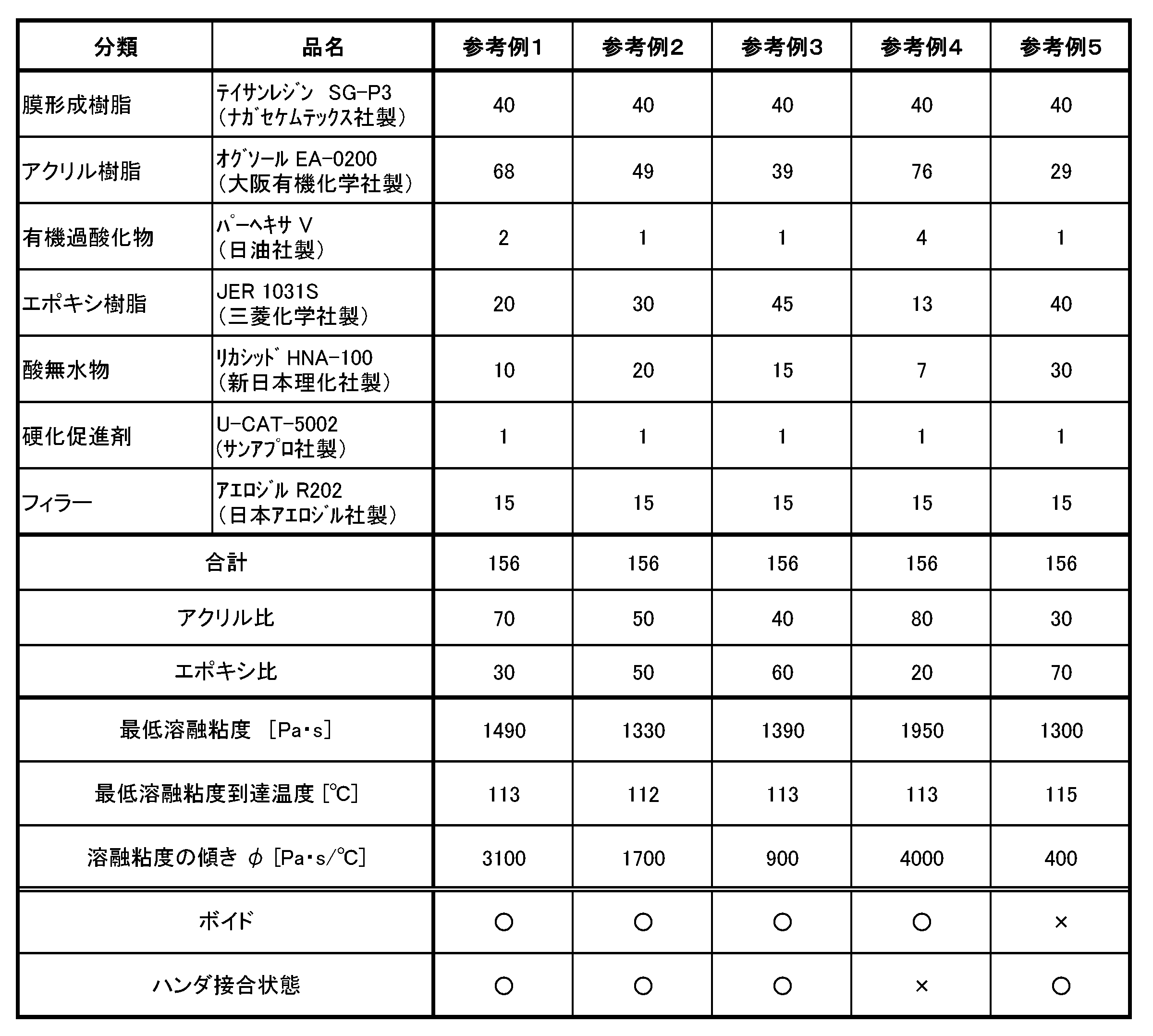
上述したとおり、本実施例では、先供給型のアンダーフィルフィルムを作製し、次いで、アンダーフィルフィルムを用いてハンダ付き電極を有する複数の上チップと、これに対向する電極を有する下チップとを図11及び図12に示すようなギャングボンディング装置を用い、一括圧着させて実装体を作製し、ボイド、ハンダ接合状態、及びフィレットについて評価した。その際のアンダーフィルフィルムの弾性率、最低溶融粘度及び溶融粘度の傾きの測定、実装体の作製、搭載時のチップズレ、ボイド、ハンダ接合、及びフィレットの評価は、次のように行った。
各アンダーフィルフィルムについて、レオメータ(TA社製ARES)を用いて、5℃/min、1Hzの条件でサンプルの弾性率、最低溶融粘度及び最低溶融粘度到達温度を測定した。そして、最低溶融粘度到達温度+10℃~最低溶融粘度到達温度+20℃の温度範囲における溶融粘度の傾きを算出した。
まず、アンダーフィルフィルムをウエハ上にプレス機にて、50℃-0.5MPaの条件で貼り合わせ、ダンシングしてハンダ付き電極を有する上チップを得た。
下チップ上に9個の上チップを一括圧着した際のチップズレを、X線装置にて目視し、チップズレが5μm以下で実質的に確認できない場合を「○」と評価し、他方、それ以上チップズレが確認できた場合を「×」と評価した。
実装体をSAT(Scanning Acoustic Tomograph, 超音波映像装置)を用いて観察した。実装体のボイド面積を確認し、ボイドが発生していないか、又は発生してもボイドの直径が100μm以下の場合を「○」と評価し、それ以上のボイドが確認できた場合を「×」と評価した。一般的に、100μmを超えたボイドが生じると、経験上、長期信頼性に悪影響を及ぼす可能性が高くなる。
実装体のサンプルを切断し、断面研磨を行い、上チップと下チップとのバンプ間のハンダの状態をSEM(Scanning Electron Microscope)観察した。下チップ側のバンプの90%以上にハンダ濡れ広がりがある場合の良好な状態を「○」と評価し、それ以外のハンダ濡れが不十分な状態を「×」と評価した。
実装体のチップ間及びチップ端部を目視にて観察し、フィレットが形成されている場合を「×」と評価し、フィレットが形成されていない場合を「○」と評価した。
参考例1に記載の樹脂組成物と同様の組成物を調整した。この組成物を、剥離処理されたPET(Polyethylene terephthalate)にバーコーターを用いて塗布し、80℃のオーブンで3分間乾燥させ、厚み18μmのアンダーフィルフィルムを作製した(カバー剥離PET(25μm)/アンダーフィルフィルム(18μm)/ベース剥離PET(50μm))。
参考例2に記載された樹脂組成物と同様な樹脂組成物を作成した。この組成物を、剥離処理されたPET(Polyethylene terephthalate)にバーコーターを用いて塗布し、80℃のオーブンで3分間乾燥させ、厚み18μmのアンダーフィルフィルムを作製した(カバー剥離PET(25μm)/アンダーフィルフィルム(18μm)/ベース剥離PET(50μm))。
参考例3に記載の樹脂組成物と同様な樹脂組成物を調整した。この組成物を、剥離処理されたPET(Polyethylene terephthalate)にバーコーターを用いて塗布し、80℃のオーブンで3分間乾燥させ、厚み18μmのアンダーフィルフィルムを作製した(カバー剥離PET(25μm)/アンダーフィルフィルム(18μm)/ベース剥離PET(50μm))。
参考例4の樹脂組成物と同様の組成物を調整した。この組成物を、剥離処理されたPET(Polyethylene terephthalate)にバーコーターを用いて塗布し、80℃のオーブンで3分間乾燥させ、厚み18μmのアンダーフィルフィルムを作製した(カバー剥離PET(25μm)/アンダーフィルフィルム(18μm)/ベース剥離PET(50μm))。
比較例5に記載の樹脂組成物の同様な樹脂組成物を調整した。この樹脂組成物を、剥離処理されたPET(Polyethylene terephthalate)にバーコーターを用いて塗布し、80℃のオーブンで3分間乾燥させ、厚み18μmのアンダーフィルフィルムを作製した(カバー剥離PET(25μm)/アンダーフィルフィルム(18μm)/ベース剥離PET(50μm))。

Claims (10)
- ハンダ付き電極が形成された複数の半導体チップを、アンダーフィルフィルムを介して前記ハンダ付き電極と対向する対向電極が形成された電子部品に搭載する搭載工程と、
前記複数の半導体チップと前記電子部品とを、前記アンダーフィルフィルムを介して一括圧着する圧着工程とを有し、
前記アンダーフィルフィルムが、エポキシ樹脂と、酸無水物と、アクリル樹脂と、有機過酸化物とを含有し、最低溶融粘度が、1000Pa・s以上2000Pa・s以下であり、最低溶融粘度到達温度より10℃高い温度から該温度より10℃高い温度までの溶融粘度の傾きが、900Pa・s/℃以上3100Pa・s/℃以下である半導体装置の製造方法。 - 前前記溶融粘度の傾きが、1700Pa・s/℃以上3100Pa・s/℃以下である請求項1記載の半導体装置の製造方法。
- 前記アクリル樹脂と前記有機過酸化物との合計質量と、前記エポキシ樹脂と前記酸無水物との合計質量との比が、7:3~5:5である請求項2記載の半導体装置の製造方法。
- 前記エポキシ樹脂が、グリシジルエーテル型エポキシ樹脂であり、
前記酸無水物が、脂環式酸無水物である請求項1乃至3のいずれか1項に記載の半導体装置の製造方法。 - 前記アクリル樹脂が、フルオレン系アクリレートであり、
前記有機過酸化物が、パーオキシケタールである請求項1乃至4のいずれか1項に記載の半導体装置の製造方法。 - 複数の半導体チップと電子部品とを、一括圧着するためのアンダーフィルフィルムであって、
エポキシ樹脂と、酸無水物と、アクリル樹脂と、有機過酸化物とを含有し、最低溶融粘度が、1000Pa・s以上2000Pa・s以下であり、最低溶融粘度到達温度より10℃高い温度から該温度より10℃高い温度までの溶融粘度の傾きが、900Pa・s/℃以上3100Pa・s/℃以下であるアンダーフィルフィルム。 - 前前記溶融粘度の傾きが、1700Pa・s/℃以上3100Pa・s/℃以下である請求項6記載のアンダーフィルフィルム。
- 前記アクリル樹脂と前記有機過酸化物との合計質量と、前記エポキシ樹脂と前記酸無水物との合計質量との比が、7:3~5:5である請求項7記載のアンダーフィルフィルム。
- 前記エポキシ樹脂が、グリシジルエーテル型エポキシ樹脂であり、
前記酸無水物が、脂環式酸無水物である請求項6乃至8のいずれか1項に記載のアンダーフィルフィルム。 - 前記アクリル樹脂が、フルオレン系アクリレートであり、
前記有機過酸化物が、パーオキシケタールである請求項6乃至9のいずれか1項に記載のアンダーフィルフィルム。
Priority Applications (4)
| Application Number | Priority Date | Filing Date | Title |
|---|---|---|---|
| KR1020177010337A KR101947293B1 (ko) | 2015-02-06 | 2016-02-05 | 반도체 장치의 제조 방법 및 언더필 필름 |
| US15/532,931 US10280347B2 (en) | 2015-02-06 | 2016-02-05 | Semiconductor device manufacturing method and underfill film |
| CN201680006768.7A CN107112254B (zh) | 2015-02-06 | 2016-02-05 | 半导体装置的制造方法及底部填充膜 |
| EP16746712.5A EP3255658B1 (en) | 2015-02-06 | 2016-02-05 | Method for manufacturing semiconductor device, and underfill film |
Applications Claiming Priority (2)
| Application Number | Priority Date | Filing Date | Title |
|---|---|---|---|
| JP2015022672A JP6438790B2 (ja) | 2015-02-06 | 2015-02-06 | 半導体装置の製造方法、及びアンダーフィルフィルム |
| JP2015-022672 | 2015-02-06 |
Publications (1)
| Publication Number | Publication Date |
|---|---|
| WO2016125881A1 true WO2016125881A1 (ja) | 2016-08-11 |
Family
ID=56564219
Family Applications (1)
| Application Number | Title | Priority Date | Filing Date |
|---|---|---|---|
| PCT/JP2016/053462 WO2016125881A1 (ja) | 2015-02-06 | 2016-02-05 | 半導体装置の製造方法、及びアンダーフィルフィルム |
Country Status (7)
| Country | Link |
|---|---|
| US (1) | US10280347B2 (ja) |
| EP (1) | EP3255658B1 (ja) |
| JP (1) | JP6438790B2 (ja) |
| KR (1) | KR101947293B1 (ja) |
| CN (1) | CN107112254B (ja) |
| TW (1) | TWI667309B (ja) |
| WO (1) | WO2016125881A1 (ja) |
Families Citing this family (9)
| Publication number | Priority date | Publication date | Assignee | Title |
|---|---|---|---|---|
| KR101837511B1 (ko) * | 2016-04-04 | 2018-03-14 | 주식회사 네패스 | 반도체 패키지 및 그 제조방법 |
| JP2018160566A (ja) * | 2017-03-23 | 2018-10-11 | 三井化学東セロ株式会社 | ギャングボンディングプロセス用アンダーフィル絶縁フィルム |
| WO2018212215A1 (ja) * | 2017-05-16 | 2018-11-22 | デクセリアルズ株式会社 | アンダーフィル材、アンダーフィルフィルム、及びこれを用いた半導体装置の製造方法 |
| US10693432B2 (en) * | 2018-05-17 | 2020-06-23 | Qualcommm Incorporated | Solenoid structure with conductive pillar technology |
| US10923365B2 (en) * | 2018-10-28 | 2021-02-16 | Richwave Technology Corp. | Connection structure and method for forming the same |
| CN114051647B (zh) * | 2020-01-29 | 2023-02-03 | 株式会社村田制作所 | 带电极的无源部件和带电极的无源部件的集合体 |
| KR102485700B1 (ko) * | 2020-12-23 | 2023-01-06 | 주식회사 두산 | 반도체 패키지용 언더필 필름 및 이를 이용하는 반도체 패키지의 제조방법 |
| US11355361B1 (en) * | 2021-04-28 | 2022-06-07 | Coretech System Co., Ltd. | Method of measuring underfill profile of underfill cavity having solder bumps |
| TWI773360B (zh) * | 2021-06-03 | 2022-08-01 | 矽品精密工業股份有限公司 | 電子封裝件及其承載結構與製法 |
Citations (3)
| Publication number | Priority date | Publication date | Assignee | Title |
|---|---|---|---|---|
| JP2002252254A (ja) * | 2001-02-26 | 2002-09-06 | Sony Chem Corp | 電気装置製造方法 |
| WO2013080708A1 (ja) * | 2011-11-29 | 2013-06-06 | 東レ株式会社 | 樹脂組成物、樹脂組成物シート、半導体装置およびその製造方法 |
| JP2013211352A (ja) * | 2012-03-30 | 2013-10-10 | Dexerials Corp | 回路接続材料、及びこれを用いた半導体装置の製造方法 |
Family Cites Families (8)
| Publication number | Priority date | Publication date | Assignee | Title |
|---|---|---|---|---|
| US5965663A (en) * | 1995-06-06 | 1999-10-12 | Kabushiki Kaisha Toshiba | Resin composition and resin-molded type semiconductor device |
| DE1025587T1 (de) * | 1997-07-21 | 2001-02-08 | Aguila Technologies Inc | Halbleiter-flipchippackung und herstellungsverfahren dafür |
| JP4170839B2 (ja) | 2003-07-11 | 2008-10-22 | 日東電工株式会社 | 積層シート |
| JP2008074928A (ja) * | 2006-09-20 | 2008-04-03 | Hitachi Chem Co Ltd | 半導体用接着フィルム及びこれを用いた半導体装置 |
| JP2012234804A (ja) * | 2011-04-21 | 2012-11-29 | Sumitomo Electric Ind Ltd | フィルム状異方導電性接着剤 |
| JP2013175546A (ja) * | 2012-02-24 | 2013-09-05 | Dexerials Corp | アンダーフィル材、及びそれを用いた半導体装置の製造方法 |
| US9287204B2 (en) * | 2012-12-20 | 2016-03-15 | Stats Chippac, Ltd. | Semiconductor device and method of bonding semiconductor die to substrate in reconstituted wafer form |
| JP6692758B2 (ja) * | 2014-02-24 | 2020-05-13 | ヘンケル アイピー アンド ホールディング ゲゼルシャフト ミット ベシュレンクテル ハフツング | 熱伝導性プリアプライアンダーフィル組成物およびその使用 |
-
2015
- 2015-02-06 JP JP2015022672A patent/JP6438790B2/ja active Active
-
2016
- 2016-02-05 EP EP16746712.5A patent/EP3255658B1/en active Active
- 2016-02-05 CN CN201680006768.7A patent/CN107112254B/zh active Active
- 2016-02-05 KR KR1020177010337A patent/KR101947293B1/ko active IP Right Grant
- 2016-02-05 WO PCT/JP2016/053462 patent/WO2016125881A1/ja active Application Filing
- 2016-02-05 US US15/532,931 patent/US10280347B2/en active Active
- 2016-02-05 TW TW105103933A patent/TWI667309B/zh active
Patent Citations (3)
| Publication number | Priority date | Publication date | Assignee | Title |
|---|---|---|---|---|
| JP2002252254A (ja) * | 2001-02-26 | 2002-09-06 | Sony Chem Corp | 電気装置製造方法 |
| WO2013080708A1 (ja) * | 2011-11-29 | 2013-06-06 | 東レ株式会社 | 樹脂組成物、樹脂組成物シート、半導体装置およびその製造方法 |
| JP2013211352A (ja) * | 2012-03-30 | 2013-10-10 | Dexerials Corp | 回路接続材料、及びこれを用いた半導体装置の製造方法 |
Non-Patent Citations (1)
| Title |
|---|
| See also references of EP3255658A4 * |
Also Published As
| Publication number | Publication date |
|---|---|
| CN107112254B (zh) | 2019-10-15 |
| EP3255658A1 (en) | 2017-12-13 |
| EP3255658A4 (en) | 2018-09-12 |
| CN107112254A (zh) | 2017-08-29 |
| JP6438790B2 (ja) | 2018-12-19 |
| KR101947293B1 (ko) | 2019-02-12 |
| EP3255658B1 (en) | 2019-09-18 |
| US10280347B2 (en) | 2019-05-07 |
| KR20170056663A (ko) | 2017-05-23 |
| TWI667309B (zh) | 2019-08-01 |
| JP2016146412A (ja) | 2016-08-12 |
| US20180079939A1 (en) | 2018-03-22 |
| TW201706383A (zh) | 2017-02-16 |
Similar Documents
| Publication | Publication Date | Title |
|---|---|---|
| JP6438790B2 (ja) | 半導体装置の製造方法、及びアンダーフィルフィルム | |
| JP5965185B2 (ja) | 回路接続材料、及びこれを用いた半導体装置の製造方法 | |
| KR101712046B1 (ko) | 언더필재, 및 이것을 사용한 반도체 장치의 제조 방법 | |
| JP6069142B2 (ja) | アンダーフィル材、及びこれを用いた半導体装置の製造方法 | |
| KR102308395B1 (ko) | 언더필재 및 이것을 사용한 반도체 장치의 제조 방법 | |
| US10062625B2 (en) | Underfill material and method for manufacturing semiconductor device using the same | |
| WO2015037631A1 (ja) | アンダーフィル材、及びこれを用いた半導体装置の製造方法 | |
| WO2015045878A1 (ja) | アンダーフィル材、及びこれを用いた半導体装置の製造方法 |
Legal Events
| Date | Code | Title | Description |
|---|---|---|---|
| 121 | Ep: the epo has been informed by wipo that ep was designated in this application |
Ref document number: 16746712 Country of ref document: EP Kind code of ref document: A1 |
|
| ENP | Entry into the national phase |
Ref document number: 20177010337 Country of ref document: KR Kind code of ref document: A |
|
| WWE | Wipo information: entry into national phase |
Ref document number: 15532931 Country of ref document: US |
|
| REEP | Request for entry into the european phase |
Ref document number: 2016746712 Country of ref document: EP |
|
| NENP | Non-entry into the national phase |
Ref country code: DE |