WO2016111322A1 - 情報入力装置 - Google Patents
情報入力装置 Download PDFInfo
- Publication number
- WO2016111322A1 WO2016111322A1 PCT/JP2016/050306 JP2016050306W WO2016111322A1 WO 2016111322 A1 WO2016111322 A1 WO 2016111322A1 JP 2016050306 W JP2016050306 W JP 2016050306W WO 2016111322 A1 WO2016111322 A1 WO 2016111322A1
- Authority
- WO
- WIPO (PCT)
- Prior art keywords
- state
- asic
- sensor
- coils
- current
- Prior art date
- Legal status (The legal status is an assumption and is not a legal conclusion. Google has not performed a legal analysis and makes no representation as to the accuracy of the status listed.)
- Ceased
Links
Images


Classifications
-
- G—PHYSICS
- G06—COMPUTING OR CALCULATING; COUNTING
- G06F—ELECTRIC DIGITAL DATA PROCESSING
- G06F3/00—Input arrangements for transferring data to be processed into a form capable of being handled by the computer; Output arrangements for transferring data from processing unit to output unit, e.g. interface arrangements
- G06F3/01—Input arrangements or combined input and output arrangements for interaction between user and computer
- G06F3/03—Arrangements for converting the position or the displacement of a member into a coded form
- G06F3/041—Digitisers, e.g. for touch screens or touch pads, characterised by the transducing means
- G06F3/0416—Control or interface arrangements specially adapted for digitisers
-
- B—PERFORMING OPERATIONS; TRANSPORTING
- B43—WRITING OR DRAWING IMPLEMENTS; BUREAU ACCESSORIES
- B43K—IMPLEMENTS FOR WRITING OR DRAWING
- B43K29/00—Combinations of writing implements with other articles
- B43K29/08—Combinations of writing implements with other articles with measuring, computing or indicating devices
-
- G—PHYSICS
- G06—COMPUTING OR CALCULATING; COUNTING
- G06F—ELECTRIC DIGITAL DATA PROCESSING
- G06F1/00—Details not covered by groups G06F3/00 - G06F13/00 and G06F21/00
- G06F1/16—Constructional details or arrangements
- G06F1/1613—Constructional details or arrangements for portable computers
- G06F1/1615—Constructional details or arrangements for portable computers with several enclosures having relative motions, each enclosure supporting at least one I/O or computing function
- G06F1/1616—Constructional details or arrangements for portable computers with several enclosures having relative motions, each enclosure supporting at least one I/O or computing function with folding flat displays, e.g. laptop computers or notebooks having a clamshell configuration, with body parts pivoting to an open position around an axis parallel to the plane they define in closed position
-
- G—PHYSICS
- G06—COMPUTING OR CALCULATING; COUNTING
- G06F—ELECTRIC DIGITAL DATA PROCESSING
- G06F1/00—Details not covered by groups G06F3/00 - G06F13/00 and G06F21/00
- G06F1/16—Constructional details or arrangements
- G06F1/1613—Constructional details or arrangements for portable computers
- G06F1/1633—Constructional details or arrangements of portable computers not specific to the type of enclosures covered by groups G06F1/1615 - G06F1/1626
- G06F1/1637—Details related to the display arrangement, including those related to the mounting of the display in the housing
- G06F1/1643—Details related to the display arrangement, including those related to the mounting of the display in the housing the display being associated to a digitizer, e.g. laptops that can be used as penpads
-
- G—PHYSICS
- G06—COMPUTING OR CALCULATING; COUNTING
- G06F—ELECTRIC DIGITAL DATA PROCESSING
- G06F1/00—Details not covered by groups G06F3/00 - G06F13/00 and G06F21/00
- G06F1/16—Constructional details or arrangements
- G06F1/1613—Constructional details or arrangements for portable computers
- G06F1/1633—Constructional details or arrangements of portable computers not specific to the type of enclosures covered by groups G06F1/1615 - G06F1/1626
- G06F1/1637—Details related to the display arrangement, including those related to the mounting of the display in the housing
- G06F1/1647—Details related to the display arrangement, including those related to the mounting of the display in the housing including at least an additional display
-
- G—PHYSICS
- G06—COMPUTING OR CALCULATING; COUNTING
- G06F—ELECTRIC DIGITAL DATA PROCESSING
- G06F1/00—Details not covered by groups G06F3/00 - G06F13/00 and G06F21/00
- G06F1/16—Constructional details or arrangements
- G06F1/1613—Constructional details or arrangements for portable computers
- G06F1/1633—Constructional details or arrangements of portable computers not specific to the type of enclosures covered by groups G06F1/1615 - G06F1/1626
- G06F1/1675—Miscellaneous details related to the relative movement between the different enclosures or enclosure parts
- G06F1/1677—Miscellaneous details related to the relative movement between the different enclosures or enclosure parts for detecting open or closed state or particular intermediate positions assumed by movable parts of the enclosure, e.g. detection of display lid position with respect to main body in a laptop, detection of opening of the cover of battery compartment
-
- G—PHYSICS
- G06—COMPUTING OR CALCULATING; COUNTING
- G06F—ELECTRIC DIGITAL DATA PROCESSING
- G06F1/00—Details not covered by groups G06F3/00 - G06F13/00 and G06F21/00
- G06F1/26—Power supply means, e.g. regulation thereof
- G06F1/32—Means for saving power
- G06F1/3203—Power management, i.e. event-based initiation of a power-saving mode
- G06F1/3206—Monitoring of events, devices or parameters that trigger a change in power modality
-
- G—PHYSICS
- G06—COMPUTING OR CALCULATING; COUNTING
- G06F—ELECTRIC DIGITAL DATA PROCESSING
- G06F1/00—Details not covered by groups G06F3/00 - G06F13/00 and G06F21/00
- G06F1/26—Power supply means, e.g. regulation thereof
- G06F1/32—Means for saving power
- G06F1/3203—Power management, i.e. event-based initiation of a power-saving mode
- G06F1/3234—Power saving characterised by the action undertaken
- G06F1/3296—Power saving characterised by the action undertaken by lowering the supply or operating voltage
-
- G—PHYSICS
- G06—COMPUTING OR CALCULATING; COUNTING
- G06F—ELECTRIC DIGITAL DATA PROCESSING
- G06F3/00—Input arrangements for transferring data to be processed into a form capable of being handled by the computer; Output arrangements for transferring data from processing unit to output unit, e.g. interface arrangements
- G06F3/01—Input arrangements or combined input and output arrangements for interaction between user and computer
- G06F3/03—Arrangements for converting the position or the displacement of a member into a coded form
- G06F3/033—Pointing devices displaced or positioned by the user, e.g. mice, trackballs, pens or joysticks; Accessories therefor
- G06F3/0354—Pointing devices displaced or positioned by the user, e.g. mice, trackballs, pens or joysticks; Accessories therefor with detection of two-dimensional [2D] relative movements between the device, or an operating part thereof, and a plane or surface, e.g. 2D mice, trackballs, pens or pucks
- G06F3/03545—Pens or stylus
-
- G—PHYSICS
- G06—COMPUTING OR CALCULATING; COUNTING
- G06F—ELECTRIC DIGITAL DATA PROCESSING
- G06F3/00—Input arrangements for transferring data to be processed into a form capable of being handled by the computer; Output arrangements for transferring data from processing unit to output unit, e.g. interface arrangements
- G06F3/01—Input arrangements or combined input and output arrangements for interaction between user and computer
- G06F3/03—Arrangements for converting the position or the displacement of a member into a coded form
- G06F3/033—Pointing devices displaced or positioned by the user, e.g. mice, trackballs, pens or joysticks; Accessories therefor
- G06F3/038—Control and interface arrangements therefor, e.g. drivers or device-embedded control circuitry
- G06F3/0383—Signal control means within the pointing device
-
- G—PHYSICS
- G06—COMPUTING OR CALCULATING; COUNTING
- G06F—ELECTRIC DIGITAL DATA PROCESSING
- G06F3/00—Input arrangements for transferring data to be processed into a form capable of being handled by the computer; Output arrangements for transferring data from processing unit to output unit, e.g. interface arrangements
- G06F3/01—Input arrangements or combined input and output arrangements for interaction between user and computer
- G06F3/03—Arrangements for converting the position or the displacement of a member into a coded form
- G06F3/041—Digitisers, e.g. for touch screens or touch pads, characterised by the transducing means
-
- G—PHYSICS
- G06—COMPUTING OR CALCULATING; COUNTING
- G06F—ELECTRIC DIGITAL DATA PROCESSING
- G06F3/00—Input arrangements for transferring data to be processed into a form capable of being handled by the computer; Output arrangements for transferring data from processing unit to output unit, e.g. interface arrangements
- G06F3/01—Input arrangements or combined input and output arrangements for interaction between user and computer
- G06F3/03—Arrangements for converting the position or the displacement of a member into a coded form
- G06F3/041—Digitisers, e.g. for touch screens or touch pads, characterised by the transducing means
- G06F3/0416—Control or interface arrangements specially adapted for digitisers
- G06F3/04166—Details of scanning methods, e.g. sampling time, grouping of sub areas or time sharing with display driving
-
- G—PHYSICS
- G06—COMPUTING OR CALCULATING; COUNTING
- G06F—ELECTRIC DIGITAL DATA PROCESSING
- G06F3/00—Input arrangements for transferring data to be processed into a form capable of being handled by the computer; Output arrangements for transferring data from processing unit to output unit, e.g. interface arrangements
- G06F3/01—Input arrangements or combined input and output arrangements for interaction between user and computer
- G06F3/03—Arrangements for converting the position or the displacement of a member into a coded form
- G06F3/041—Digitisers, e.g. for touch screens or touch pads, characterised by the transducing means
- G06F3/046—Digitisers, e.g. for touch screens or touch pads, characterised by the transducing means by electromagnetic means
Definitions
- the present invention relates to an information input device capable of acquiring information written by a user by digitizing a movement path of the writing tool when the user writes on a paper medium with a writing tool.
- Patent Document 1 discloses an information input device having two housings incorporating a plurality of coils.
- the information input device is driven using a battery as a power source.
- the two housings are folded when not in use and are opened when used.
- a booklet-shaped paper medium is placed on the two housings in the open state.
- the information input device generates an induced magnetic field by energizing the plurality of first coils built in the two casings.
- An induced current flows through the second coil built in the writing instrument in accordance with the induced magnetic field generated from the first coil of the information input device.
- the writing instrument generates an induced magnetic field in response to an induced current flowing through the second coil.
- the information input device detects the induced magnetic field generated from the writing instrument by the plurality of first coils.
- the information input device specifies the position of the writing instrument.
- the information input device preferably operates in the power saving mode when the two cases are not used.
- the information input device needs to detect that the two housings are folded.
- a case will be exemplified in which a power switch is added to the information input device and the information input device is notified by the power switch that two housings are folded. In this case, the user has to operate the power switch manually, which is troublesome.
- a case where a sensor is added to the information input device and the information input device detects that the two housings are folded by the sensor will be described as an example. In this case, it is necessary to newly add a sensor to the information input device. Therefore, there is a problem that the cost of the information input device increases.
- An object of the present invention is to provide an information input device that can suppress power consumption when two housings are folded with a simple configuration.
- the information input device of the present invention is two regions in which a plurality of coils are arranged along a plane, and can be switched between a folded state in which each region is opposed and a spread state in which each region is not opposed 2
- a detection unit having two regions, a first determination unit that determines whether the two regions of the detection unit are in the folded state or the spread state, and the folded state by the first determination unit
- switching means for switching the state of the detection unit from a normal state with relatively large current consumption to a relatively low power saving state, the detection unit in the normal state
- the transmission / reception in which one of the two regions is alternately switched between a transmission state in which current is supplied to the plurality of coils and a reception state in which induction currents of the plurality of coils can be detected.
- the other is switched to the second state in which the other is in the transmission / reception state, and the first determination means detects the induced current in the plurality of coils in any one of the second regions in the continuous reception state. If not, the spread state is determined, and if the induced current is detected, the folded state is determined.
- the detection unit generates an induced magnetic field from a plurality of coils in a transmission state.
- the induced magnetic field generates an induced current in a coil built in the writing instrument.
- the writing instrument generates an induced magnetic field based on the induced current generated in the coil.
- the induced magnetic field generated from the writing instrument generates an induced current in the plurality of coils in the reception state of the detection unit.
- the detection unit can specify the position of the writing instrument based on the position of the coil where the induced current is generated.
- the information input device detects the position of the writing instrument in all of the two areas by switching each of the two areas to the first state and the second state.
- the information input device determines that the two regions are in the spread state when the induced current is not detected by the plurality of coils in the continuous reception state.
- the two regions are in the folded state, induced magnetic fields generated from the plurality of coils in the transmission / reception state act on the plurality of coils in the continuous reception state, and an induced current flows through the coils in the continuous reception state. For this reason, the information input device determines that the two regions are in the folded state when the induced current is detected in the plurality of coils in the continuous reception state.
- the information input device can determine whether the two regions are in the spread state or the folded state by using the detection unit for detecting the position of the writing instrument as it is. Therefore, the information input device can suppress power consumption when the two housings are folded with a simple configuration by switching to the power saving state when it is determined that the information input device is in the folded state.
- the switching means further includes first switching means for switching to a first power saving state in which current is supplied to only some of the plurality of coils in one of the two regions. May be.
- first switching means for switching to a first power saving state in which current is supplied to only some of the plurality of coils in one of the two regions. May be.
- the information input device can determine that the two regions are in the folded state even when a current is passed through only some of the coils. Therefore, the information input device can appropriately suppress power consumption in a state where the two regions are folded by suppressing power consumption caused by energizing the plurality of coils.
- the first switching means may switch to the first power saving state in which a current is intermittently supplied to only some of the plurality of coils.
- the information input device can further suppress power consumption caused by energizing some of the plurality of coils. Therefore, the information input device can more appropriately suppress power consumption in a state where the two areas are folded.
- the switching means may further comprise second switching means for switching to a second power saving state in which energization of the plurality of coils in each of the two regions is stopped.
- the information input device can suppress the amount of current flowing through the plurality of coils to a minimum. Therefore, the information input device can greatly suppress power consumption in a state where the two areas are folded.
- the switching unit may maintain the first power saving state when an elapsed time after the first determination unit determines that the state is the folded state is shorter than a predetermined time.
- the information input device can appropriately detect the spread state when the two regions are once folded and then returned to the spread state.
- the second switching means may switch to the second power saving state when the elapsed time from the time when the first determination means determines that the folded state is longer than a predetermined time.
- the information input device can significantly reduce power consumption after the elapsed time in the folded state becomes a predetermined time or longer.
- a control unit that performs control to switch the detection unit between the first state and the second state is provided, and the second switching unit is configured to turn off the power supplied to the control unit. You may switch to 2 power saving states. In this case, since the information input device can also suppress the power consumption of the control unit, the power consumption in a state where the two regions are folded can be further suppressed.
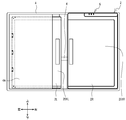
- FIG. 2 is a plan view of a reading device 2.
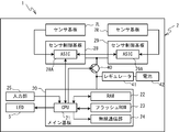
- FIG. 2 is a block diagram showing an electrical configuration of a reading device 2.
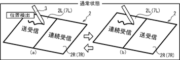
- FIG. It is a figure which shows the reader 2 in a normal state. It is a figure which shows the reading apparatus 2 in a normal state, a 1st power saving state, and a 2nd power saving state.
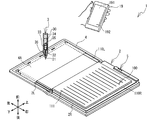
- FIG. 1 The outline of the handwriting input system 1 according to the present embodiment will be described with reference to FIGS. 1 and 2.
- the upper left side, lower right side, upper side, lower side, upper right side, and lower left side in FIG. 1 are defined as the left side, right side, front side, rear side, upper side, and lower side of the reading apparatus 2, respectively.
- the handwriting input system 1 mainly includes a reading device 2, an electronic pen 3, a smartphone 19, and the like.
- the reading device 2 is a thin and lightweight handwriting input device that can be folded.
- the user uses the electronic pen 3 to write a line drawing on each of the plurality of sheets 111 of the paper medium 100 mounted on the reading device 2.
- the reading device 2 acquires a plurality of positions of the electronic pen 3 in the writing process.
- the smartphone 19 acquires a plurality of positions specified by the reading device 2.
- the smartphone 19 specifies a line drawing written on each of the plurality of sheets 111 with the electronic pen 3 based on the acquired plurality of positions.
- the smartphone 19 creates an image file of an image including at least the specified line drawing.
- the user of the smartphone 19 inputs an operation for selecting any one of the plurality of created image files via the touch panel 191.
- the smartphone 19 causes the display 192 to display an image corresponding to the selected image file.
- the user can visually recognize an image including a line drawing having the same shape as the line drawing written on each of the plurality of sheets 111 with the electronic pen 3 via the display 192.
- the reading device 2 mainly includes a pair of left and right left reading devices 2L, a right reading device 2R, a flat cable 6 and a cover 4.
- the left reading device 2L and the right reading device 2R are rectangular thin plates.
- the left reading device 2L and the right reading device 2R are arranged on the front surface of the cover 4 so as to be spread in the left-right direction.
- the left reading device 2L and the right reading device 2R are electrically connected by a flat cable 6.
- each of the left reading device 2L and the right reading device 2R when the flat cable 6 is bent or extended, each of the left reading device 2L and the right reading device 2R is in a folded state in which the flat cables 6 face each other and in a spread state in which the flat cables 6 do not face each other. It can be deformed between.
- the left reading device 2L and the right reading device 2R are in a state of being opened when in use and are in a state of being folded when not in use.
- the left reading device 2L and the right reading device 2R are arranged side by side in the left-right direction in a spread state.
- the right reading device 2R includes three LEDs 5 at the upper end. The LED 5 can notify the user of the state of the reading device 2.
- the cover 4 includes a bag-like bag portion 4A on the left side.
- the left reading device 2L is detachably attached to the cover 4 by being inserted into the bag portion 4A.
- the right reading device 2R is attached to the right front surface of the cover 4 with a resin film or the like.
- a paper medium 100 is detachably mounted on the front surface of the reading device 2 in a state where the left reading device 2L and the right reading device 2R are opened.
- the paper medium 100 is a booklet that can be spread.
- the paper medium 100 includes a pair of front covers (a front cover 110L and a back cover 110R) and a plurality of papers 111.
- Each of the front cover 110L, the back cover 110R, and the plurality of sheets 111 has a rectangular shape.
- the front cover 110L, the back cover 110R, and the plurality of sheets 111 are bound on one side extending in the longitudinal direction.
- the bound portion of the plurality of sheets 111 extends in the vertical direction.
- the paper medium 100 is an A5 size notebook.
- the paper medium 100 is placed in a detection area 201L (see FIG. 2) in which the front cover 110L is the front surface of the left reading device 2L.
- the paper medium 100 is placed in a detection area 201R (see FIG. 2) in which the back cover 110R is the front surface of the right reading device 2R.
- the paper medium 100 is mounted on the reading device 2 in a state where the left reading device 2L and the right reading device 2R are opened.
- the paper medium 100 is loaded in a state where the paper medium 100 is positioned on the reading device 2 by an adhesive tape or the like.
- the user can write a line drawing on each of the plurality of sheets 111 of the paper medium 100 using the electronic pen 3.
- the electronic pen 3 is a known electromagnetic induction type electronic pen.
- the electronic pen 3 mainly includes a cylindrical body 30, a core body 31, a coil 32, a variable capacitor 33, a substrate 34, a capacitor 35, and an ink storage unit 36.
- the cylinder 30 has a columnar shape.
- the cylindrical body 30 accommodates therein a part of the core body 31, the coil 32, the variable capacitor 33, the substrate 34, the capacitor 35, and the ink storage unit 36.
- the core body 31 is provided at the tip of the electronic pen 3.
- the core body 31 is urged toward the distal end side of the electronic pen 3 by an elastic member (not shown).
- the distal end portion of the core body 31 protrudes outside the cylindrical body 30.
- the rear end side of the core 31 is connected to an ink storage portion 36 that stores ink.
- the ink storage unit 36 supplies ink to the core body 31.
- the coil 32 is held between the core body 31 and the variable capacitor 33 while being wound around the ink storage portion 36.
- the variable capacitor 33 is fixed inside the electronic pen 3 by the substrate 34.
- a capacitor 35 is mounted on the substrate 34. The capacitor 35 and the variable capacitor 33 are connected in parallel to the coil 32 and constitute a known resonance circuit.
- the smartphone 19 includes a touch panel 191 and a display 192.
- the touch panel 191 is used for inputting various instructions.
- the display 192 can display an image corresponding to the image file.
- a general-purpose PC or a tablet PC may be used instead of the smartphone 19.
- the reading device 2 includes sensor boards 7L and 7R, a main board 20, sensor control boards 28 and 29, an input unit 25, three LEDs 5, a transistor 40, a regulator 41, and a battery 42.
- the sensor substrate 7L is provided in the left reading device 2L and at a position corresponding to the detection region 201L (see FIG. 2).
- the sensor substrate 7R is provided in the right reading device 2R and at a position corresponding to the detection region 201R (see FIG. 2). In a state where the left reading device 2L and the right reading device 2R are opened, the sensor substrates 7L and 7R are also opened.
- the sensor substrates 7L and 7R are also folded.
- a state where the sensor substrates 7L and 7R are folded is referred to as a “folded state”
- a state where the sensor substrates 7L and 7R are opened is referred to as a “spread state”.
- the input unit 25 and the three LEDs 5 are provided in the right reading device 2R.
- the colors of the three LEDs 5 are yellow, green, and red.
- the main board 20 includes a CPU 21, a RAM 22, a flash ROM 23, and a wireless communication unit 24.
- the RAM 22, flash ROM 23, and wireless communication unit 24 are electrically connected to the CPU 21.
- the CPU 21 controls the reading device 2.
- the RAM 22 temporarily stores various data such as calculation data.
- the flash ROM 23 stores stroke data.
- the flash ROM 23 stores a program that the CPU 21 executes to control the reading device 2.
- the reading device 2 can receive a program from an external device (not shown) or a network that can communicate via a wireless communication unit 24 described later, and can install the program in the flash ROM 23.
- the reading device 2 may include a medium reading device (for example, a memory card slot) not shown.
- the reading device 2 may read a program stored in a storage medium (for example, a memory card) with the medium reading device and install it in the flash ROM 23.
- the wireless communication unit 24 is a controller for executing short-range wireless communication with an external electronic device.
- Bluetooth registered trademark
- the input unit 25 and the three LEDs 5 are electrically connected to the CPU 21.
- the input unit 25 is a switch for inputting an instruction to the reading device 2.
- a plurality of elongated loop coils are arranged in each of the vertical direction and the horizontal direction.
- the sensor board 7L is electrically connected to the ASIC 28A of the sensor control board 28.
- the ASIC 28A controls energization of current to the plurality of loop coils of the sensor substrate 7L.
- the sensor board 7R is electrically connected to the ASIC 29A of the sensor control board 29.
- the ASIC 29A controls current supply to the plurality of loop coils of the sensor substrate 7R.
- the ASIC 28A operates as a master, and the ASIC 29A operates as a slave.
- the ASIC 28A is directly connected to the CPU 21.
- the ASIC 29A is connected to the ASIC 28A.
- the ASICs 28A and 29A contain a ROM (not shown) in which a program is stored.
- the battery 42 is a power source for driving the main board 20 and the sensor control boards 28 and 29.
- the regulator 41 stabilizes the voltage of the battery 42.
- the power of the battery 42 whose voltage is stabilized by the regulator 41 is directly supplied to the main board 20. Further, the power of the battery 42 stabilized by the regulator 41 is supplied to the sensor control boards 28 and 29 via the transistor 40.
- the transistor 40 can control ON / OFF of power supply to the sensor control boards 28 and 29.
- the CPU 21 is connected to the base of the transistor 40. The CPU 21 can switch ON / OFF of power supply to the sensor control boards 28 and 29 by the transistor 40.
- the reading device 2 is used as a two-page spread state of the sensor boards 7L and 7R.
- the ASICs 28A and 29A energize a current having a specific frequency to each of the plurality of loop coils of the sensor substrates 7L and 7R. As a result, a magnetic field is generated from the loop coil that is energized.
- the plurality of loop coils of the sensor boards 7L and 7R are divided into a plurality of regions each having a specific size.
- a plurality of loop coils included in each region are referred to as “section coils”.
- the energization of the current is performed simultaneously with respect to the plurality of loop coils included in the segment coil and sequentially for each of the plurality of segment coils.
- the ASIC 28A selects any one of the plurality of section coils of the sensor substrate 7L.
- the ASIC 28A energizes the plurality of loop coils included in the selected segment coil, and then stops the current.
- the ASIC 29A selects any one of the plurality of section coils of the sensor substrate 7R.
- the ASIC 29A stops the current after energizing the plurality of loop coils included in the selected segment coil.
- the ASICs 28A and 29A select one by one from the plurality of segment coils in order, and repeat energization and stop of the current to the plurality of loop coils included in the selected segment coil. As a result, a magnetic field is generated from a plurality of loop coils included in the section coil to which a current is applied.
- the user performed an operation of writing a line drawing on the paper 111 on the left reading device 2L using the electronic pen 3 in a state where a current is applied to a plurality of loop coils included in a specific section coil of the sensor substrate 7L.
- the electronic pen 3 comes close to the sensor substrate 7L.
- the resonance circuit of the electronic pen 3 resonates by electromagnetic induction and generates an induction magnetic field.
- the ASIC 28A After the ASIC 28A stops energizing the current to the plurality of loop coils included in the specific section coil of the sensor board 7L, the ASIC 28A generates the induced current flowing in the plurality of loop coils of the sensor board 7L by the induced magnetic field generated from the electronic pen 3. To detect. The detected induced current is amplified and detected by the ASIC 28A, and then output to the CPU 21 as a detection result. The CPU 21 detects the position of the electronic pen 3 on the left reading device 2L based on the detection result output from the ASIC 28A.
- the electronic pen 3 when the electronic pen 3 is used to write a line drawing on the paper 111 on the left reading device 2L including the sensor substrate 7L, writing pressure is applied to the core 31.
- the inductance of the coil 32 changes according to the writing pressure applied to the core body 31.
- the resonance frequency of the resonance circuit of the electronic pen 3 changes according to the writing pressure applied to the core 31.
- the CPU 21 detects a change (phase change) in the resonance frequency and determines whether or not the electronic pen 3 is in contact with each of the plurality of sheets 111 of the sheet medium 100.
- the CPU 21 can determine whether or not a line drawing is written on each of the plurality of sheets 111 of the paper medium 100.
- the same processing as described above is executed by the ASIC 29A and the sensor substrate 7R.
- the CPU 21 detects the position of the electronic pen 3 on the right reading device 2R and whether or not a line drawing is being written by the electronic pen 3.
- the ASIC 28A selects one of the plurality of section coils of the sensor substrate 7L.
- the ASIC 28A energizes a plurality of loop coils included in the selected segment coil, and then stops energization.
- the ASIC 28A repeats energization and stop of current to a plurality of loop coils included in the selected segment coil while sequentially changing the segment coil to be selected.
- the ASIC 28A determines whether the induced current is detected by any of the plurality of loop coils of the sensor substrate 7L. The above processing is repeatedly executed until all of the plurality of section coils on the sensor substrate 7L are selected (a).
- a state in which current is supplied to a plurality of loop coils included in a selected segment coil among the plurality of loop coils is referred to as a “transmission state”.
- a state where the current supply to the plurality of loop coils included in the selected section coil is stopped and the induced current can be detected is referred to as a “reception state”.
- a state in which the transmission state and the reception state are alternately switched in the sensor boards 7L and 7R is referred to as a “transmission / reception state”.
- FIG. 4A shows that the sensor substrate 7L is in a transmission / reception state.
- the sensor substrate 7L has the induction generated in any of the plurality of loop coils in the reception state.
- Detect current The CPU 21 detects the position of the electronic pen 3 on the left reading device 2L based on the detection result output from the ASIC 28A.
- the ASIC 28A controls the sensor substrate 7L to be in a transmission / reception state
- the ASIC 29A stops energization of the current to the plurality of loop coils and maintains a state where the induced current can be detected.
- the state where the current supply to the plurality of loop coils is stopped and the state in which the induced current can be detected is referred to as “continuous reception state”.
- FIG. 4A shows that the sensor substrate 7R is in a continuous reception state.
- FIG. 4A illustrates a case where the writing operation with the electronic pen 3 is performed on the paper 111 on the right reading device 2R including the sensor substrate 7R in the continuous reception state.
- no magnetic field is generated from the plurality of loop coils of the sensor substrate 7R, and therefore no induced magnetic field is generated from the nearby electronic pen 3.
- no induced current flows through the plurality of loop coils of the sensor substrate 7R, and thus the CPU 21 cannot detect the position of the electronic pen 3.
- the ASIC 28A controls the sensor board 7L and controls the ASIC 29A, so that the sensor board 7L is in a transmission / reception state and the sensor board 7R is in a continuous reception state (a), and the sensor board 7L is in continuous reception. And the state (b) in which the sensor substrate 7R is in the transmission / reception state are alternately switched. As a result, the sensor boards 7L and 7R are alternately placed in a transmission / reception state in which the position of the electronic pen 3 can be detected. As a result, the CPU 21 detects the position of the electronic pen 3 even when the writing operation is performed with the electronic pen 3 on the paper 111 on any of the left reading device 2L and the right reading device 2R.
- the line drawing is in a written state.
- the state (a) in which the sensor board 7L is in a transmission / reception state and the sensor board 7R is in a continuous reception state and the state (b) in which the sensor board 7L is in a continuous reception state and the sensor board 7R is in a transmission / reception state are alternately performed.
- the switching state is referred to as “normal state”.
- the operation when the sensor substrates 7L and 7R change between the spread state (c) and the folded states (d) to (f) will be described.
- the spread state (c) for example, no magnetic field is generated from the plurality of loop coils in the sensor substrate 7L in the continuous reception state, and no induction magnetic field is generated from the electronic pen 3. Accordingly, no induced current flows through the plurality of loop coils of the sensor substrate 7L.
- the case where the sensor boards 7L and 7R are in a folded state and the sensor board 7L in the continuous reception state is overlaid on the sensor board 7R in the transmission / reception state is illustrated.
- the plurality of loop coils of the sensor substrate 7L are affected by a magnetic field generated in response to current flowing through the plurality of loop coils of the sensor substrate 7R, and an induced current flows.
- the ASIC 28A detects that the induced current is flowing through the plurality of loop coils of the sensor board 7L in the continuous reception state, the ASIC 28A determines that the sensor boards 7L and 7R are in the folded state.
- the plurality of loop coils of the sensor board 7L are included in the plurality of loop coils of the sensor board 7R.
- a magnetic field generated in response to a current being applied to the element acts, and an induced current flows.
- the ASIC 29A outputs a notification signal to the ASIC 28A when detecting that the induced current flows through the plurality of loop coils of the sensor substrate 7R in the continuous reception state.
- the notification signal output from the ASIC 29A to the ASIC 28A in response to the detection of the induction current flowing through the plurality of loop coils of the sensor board 7R in the continuous reception state is referred to as “current detection signal”.
- the ASIC 28A detects the current detection signal output from the ASIC 29A, the ASIC 28A determines that the sensor boards 7L and 7R are in the folded state.
- the ASIC 28A determines that the sensor boards 7L and 7R are in the folded state, the ASIC 28A only applies to the section coil 51 arranged on the side separated from the sensor board 7R in the spread state among the plurality of section coils of the sensor board 7L. Energize the current.
- a state in which a current is supplied only to the sorting coil 51 is referred to as a “continuous transmission state”.
- the timing when the current is supplied to the segment coil 51 when the sensor substrate 7L is in the continuous transmission state is the same as the timing when the current is supplied to the segment coil 51 when the sensor substrate 7L is in the transmission / reception state. is there. That is, in the sensor board 7L, no current is supplied in the continuous transmission state during the period in which current is supplied to the plurality of division coils other than the division coil 51 in the transmission / reception state. In the sensor board 7L, the current is supplied in the continuous transmission state only at the timing when the current is supplied to the sorting coil 51 in the transmission / reception state. That is, in the continuous transmission state, a current is intermittently supplied to the sorting coil 51 and a magnetic field is intermittently generated. Therefore, the power consumption of the sensor board 7L is smaller in the continuous transmission state than in the transmission / reception state by the amount of current supplied to the plurality of segment coils other than the segment coil 51.
- the ASIC 28A outputs a control signal to the ASIC 29A in a state where the sensor board 7L is operated in a continuous transmission state.
- the control signal output from the ASIC 28A to the ASIC 29A in a state where the sensor board 7L is operated in the continuous transmission state is referred to as a “first control signal”.
- the ASIC 29A detects the first control signal output from the ASIC 28A, the ASIC 29A sets the sensor board 7R to the continuous reception state.
- a magnetic field that is intermittently generated in response to the current flowing through the segment coil 51 of the sensor board 7L is applied to the plurality of loop coils of the sensor board 7R. Acts and an induced current flows.
- the ASIC 29A detects that an induced current flows through the plurality of loop coils of the sensor substrate 7R in the continuous reception state
- the ASIC 29A outputs a current detection signal to the ASIC 28A.
- the ASIC 28A detects the current detection signal from the ASIC 29A, the ASIC 28A continuously operates the sensor board 7L in the continuous transmission state.
- a state in which the sensor substrate 7L operates in the continuous transmission state and the sensor substrate 7R operates in the continuous reception state is referred to as a “first power saving state”.
- the magnetic field generated in the segment coil 51 of the sensor board 7L in the continuous transmission state is a plurality of the sensor boards 7R in the continuous reception state. No effect on the loop coil. For this reason, the induced current does not flow through the plurality of loop coils of the sensor substrate 7R.
- the ASIC 29A detects that the induced current does not flow through the plurality of loop coils of the sensor substrate 7R, the ASIC 29A stops outputting the current detection signal to the ASIC 28A. When the current detection signal is no longer detected, the ASIC 28A determines that the sensor boards 7L and 7R are in the spread state.
- the ASIC 28A returns the state of the sensor boards 7L and 7R from the first power saving state to the normal state. Specifically, the ASIC 28A controls the sensor board 7L and controls the ASIC 29A, whereby the sensor board 7L is in a transmission / reception state and the sensor board 7R is in a continuous reception state (a) (see FIG. 4). The state (b) (see FIG. 4), (c) (see FIG. 5) in which the sensor board 7L is in a continuous reception state and the sensor board 7R is in a transmission / reception state is alternately switched.
- the CPU 21 controls the transistor 40 when the ASIC 28A operates the sensor substrates 7L and 7R in the first power saving state for a predetermined time or more, and controls the transistor 40, and the sensor control substrate from the battery 42 via the regulator 41.
- the power supplied to 28 and 29 is turned off (f). In this case, power is not supplied to the ASICs 28A and 29A, and the current supply to the plurality of loop coils of the sensor boards 7L and 7R is all stopped.
- the power consumption of the sensor board 7L is further reduced compared to the continuous transmission state by the amount of current that is passed through the segment coil 51 in the continuous transmission state. Furthermore, the power consumed by the ASICs 28A and 29A is also suppressed.
- a state in which energization of current to each of the plurality of loop coils of the sensor substrates 7L and 7R is stopped is referred to as a “second power saving state”.
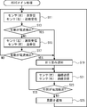
- the ASIC main process executed by the ASIC 28A will be described with reference to FIG.
- the ASIC main process is started when the ASI 28A executes a program stored in a ROM (not shown) built in the ASIC 28A.
- the power supply to the ASIC 28A is turned on when the CPU 21 executes the process of S41 (see FIG. 7), and is turned off when the process of S51 (see FIG. 7) is executed. That is, the execution time of the ASIC main process by the ASIC 28A is controlled by the CPU 21. Details will be described later.
- the ASIC 28A sets the sensor board 7L to the transmission / reception state (S11).
- the ASIC 28A outputs a first control signal to the ASIC 29A in order to place the sensor board 7R in the continuous reception state (S11).
- the ASIC 29A detects the first control signal, the ASIC 29A sets the sensor board 7R in a continuous reception state (see FIG. 4A).
- the ASIC 28A determines whether or not an induced current is flowing through the plurality of loop coils of the sensor substrate 7R in the continuous reception state based on whether the current detection signal output from the ASIC 29A is detected.
- the ASIC 28A detects the current detection signal
- the ASIC 28A determines that the induced current is flowing in the plurality of loop coils of the sensor substrate 7R (S13: YES). In this case, the ASIC 28A advances the process to S19.
- the ASIC 28A determines that the induced current does not flow through the plurality of loop coils of the sensor substrate 7R (S13: NO). In this case, the ASIC 28A sets the sensor board 7L to the continuous reception state (S15).
- the ASIC 28A outputs a control signal to the ASIC 29A in order to place the sensor board 7R in a transmission / reception state (S15).
- the control signal transmitted from the ASIC 28A to the ASIC 29A for setting the sensor board 7R to the transmission / reception state is referred to as “second control signal”.
- the ASIC 29A detects the second control signal, the ASIC 29A sets the sensor board 7R in a transmission / reception state (see FIGS. 4B, 5C, and 5D).
- the ASIC 28A determines whether or not an induced current is flowing through the plurality of loop coils of the sensor board 7L in the continuous reception state.
- the process proceeds to S19.
- the ASIC 28A determines that no induced current is flowing through the plurality of loop coils of the sensor substrate 7L (S17: NO)
- the process returns to S11. Note that the state of the sensor boards 7L and 7R when the processes of S11 and S15 are executed corresponds to the normal state (see FIGS. 4A, 4B, 5C, and 5D).
- a signal for notifying that the sensor boards 7L and 7R are in the folded state Is output to the CPU 21 (S19).
- a signal for notifying that the sensor boards 7L and 7R are in the folded state is referred to as a “folding notification signal”.
- the ASIC 28A sets the sensor board 7L to the continuous transmission state (S21).
- the ASIC 28A outputs a first control signal to the ASIC 29A in order to place the sensor board 7R in the continuous reception state (S21).
- the ASIC 29A detects the first control signal, the ASIC 29A sets the sensor substrate 7R to the continuous reception state (see FIG. 5E).
- the sensor boards 7L and 7R when the process of S21 is performed correspond to the first power saving state.
- the ASIC 28A determines whether or not an induced current is flowing through the plurality of loop coils of the sensor substrate 7R in the continuous reception state based on whether the current detection signal output from the ASIC 29A is detected.
- the ASIC 28A detects the current detection signal
- the ASIC 28A determines that the induced current is flowing in the plurality of loop coils of the sensor substrate 7R (S23: YES). In this case, the ASIC 28A returns the process to S21.
- the ASIC 28A does not detect the current detection signal
- the ASIC 28A determines that the induced current does not flow through the plurality of loop coils of the sensor substrate 7R (S23: NO).
- the ASIC 28A outputs a signal for notifying that the sensor boards 7L and 7R are in the spread state to the CPU 21 (S25).
- a signal for notifying that the sensor substrates 7L and 7R are in the spread state is referred to as a “spread notification signal”.
- the ASIC 28A returns the process to S11.
- the ASIC 28A executes a process (not shown) for detecting the position of the electronic pen 3 in parallel with the ASIC main process.
- a process for detecting the position of the electronic pen 3 in parallel with the ASIC main process.
- the detection result is output to the CPU 21.
- the CPU main process executed by the CPU 21 will be described with reference to FIG.
- the CPU main process is started when the CPU 21 executes the program stored in the flash ROM 23 when the supply of power to the CPU 21 is started.
- the CPU 21 controls the voltage of the signal output to the transistor 40 and turns on the power supply to the sensor control boards 28 and 29. As a result, power is supplied to the ASICs 28A and 29A (S41).
- the ASIC 28A starts the ASIC main process (see FIG. 6).
- the reading device 2 starts operating in a normal state.
- CPU21 judges whether the folding notification signal output from ASIC28A was detected (S43). CPU21 returns a process to S43, when it is judged that a folding notification signal is not detected (S43: NO). When it is determined that the folding notification signal is detected (S43: YES), the CPU 21 determines whether the spread notification signal is received (S45). CPU21 returns a process to S43, when it is judged that the spread notification signal was detected (S45: YES).
- the CPU 21 determines whether or not a predetermined time has elapsed since the detection of the folding notification signal by the process of S43 (S49). CPU21 returns a process to S45, when it is judged that predetermined time has not passed (S49: NO).
- the CPU 21 detects the folding notification signal in the process of S43 and then determines that a predetermined time has passed without detecting the spread notification signal (S45: NO) (S49: YES), the signal output to the transistor 40
- the power supply to the sensor control boards 28 and 29 is turned off.
- the supply of power to the ASICs 28A and 29A is turned off (S51).
- the ASIC 28A stops the ASIC main process (see FIG. 6). Further, the current supply to the plurality of loop coils of the sensor boards 7L and 7R is stopped. Note that the state of the sensor boards 7L and 7R when the process of S51 is performed corresponds to the second power saving state (see FIG. 5F).
- CPU21 judges whether operation which turns ON the power supply of the reader 2 was detected via the input part 25 (S53). If the CPU 21 determines that an operation to turn on the power is not detected (S53: NO), it returns the process to S53. If the CPU 21 determines that an operation to turn on the power has been detected (S53: YES), it returns the process to S41.
- the CPU 21 controls the voltage of the signal output to the transistor 40 and turns on the power supply to the sensor control boards 28 and 29 (S41). In addition, when the CPU 21 executes the process of S41, the sensor boards 7L and 7R resume the operation in the normal state. The CPU 21 repeats the process.
- the CPU 21 executes a process (not shown) for detecting the position of the electronic pen 3 in parallel with the CPU main process.
- the position of the loop coil that detected the electronic pen 3 is specified based on the detection result output from the ASIC 28A, and the position of the electronic pen 3 is detected. Further, whether or not the electronic pen 3 is in contact with the paper 111 is determined based on the change in the resonance frequency. Thus, it is determined whether or not a line drawing is written on the paper 111. When it is determined that the line drawing is written, coordinate data indicating the position of the electronic pen 3 is stored in the flash ROM 23.
- the reading device 2 generates an induction magnetic field from the plurality of loop coils of the sensor boards 7L and 7R in the transmission state.
- the induced magnetic field generates an induced current in the coil 32 built in the electronic pen 3.
- the electronic pen 3 generates an induced magnetic field based on the induced current generated in the coil 32.
- the induced magnetic field generated from the electronic pen 3 causes induced currents in a plurality of loop coils of the sensor substrates 7L and 7R in the reception state.
- the CPU 21 specifies the position of the electronic pen 3 based on the position of the loop coil in which the induced current is generated among the plurality of loop coils of the sensor substrates 7L and 7R.
- the ASIC 28A alternately switches between a state in which the sensor board 7L is in a transmission / reception state and the sensor board 7R is in a continuous reception state, and a state in which the sensor board 7L is in a continuous reception state and the sensor board 7R is in a transmission / reception state.
- the CPU 21 can detect the position of the electronic pen 3 with all of the left reading device 2L and the right reading device 2R.
- the ASIC 28A determines that the sensor boards 7L and 7R are in the spread state when the induced current does not flow through the plurality of coils in the continuous reception state (S13: NO, S17: NO).
- the sensor boards 7L and 7R are in the folded state, induced magnetic fields generated from the plurality of coils in the transmission / reception state act on the plurality of coils in the continuous reception state. An induced current flows through the coil in the continuous reception state. For this reason, the ASIC 28A determines that the sensor boards 7L and 7R are in the folded state when the induced current is detected in the plurality of coils in the continuous reception state (S13: YES, S17: YES).
- the ASIC 28A can determine whether the sensor substrates 7L and 7R are in a double-folded state or a folded state by using the sensor substrates 7L and 7R used for detecting the position of the electronic pen 3 as they are. .
- the ASIC 28A switches to the first power saving state when the sensor boards 7L and 7R are in the folded state. Thereby, the power consumption when the sensor substrates 7L and 7R are folded can be suppressed with a simple configuration.
- ASIC 28A operates the sensor board 7L in the continuous transmission state when operating the sensor boards 7L and 7R in the first power saving state.
- the current is intermittently supplied to only one section coil 51 among the plurality of section coils included in the plurality of loop coils of the sensor substrate 7L (S21).
- the ASIC 28A can suppress the power consumption of the sensor board 7L as compared with the case where the sensor board 7L is operated in the transmission / reception state.
- the ASIC 28A determines that the induced current flows through the plurality of loop coils of the sensor substrate 7R even when the current is applied only to the segment coil 51 of the sensor substrate 7L, so that the sensor substrates 7L and 7R are in the folded state. Can be specified.
- the ASIC 28A can appropriately suppress the power consumption of the sensor board 7L while continuously monitoring that the sensor boards 7L and 7R are in the folded state.
- the CPU 21 turns off the supply of power from the battery 42 to the sensor control boards 28 and 29 (S51). . Thereby, the CPU 21 operates the sensor boards 7L and 7R in the second power saving state. In this case, since the current supply to the plurality of loop coils of the sensor substrates 7L and 7R is also stopped, the CPU 21 can greatly suppress power consumption when the reading device 2 is in the folded state.
- the CPU 21 continues the sensor boards 7L and 7R in the first power saving state when the elapsed time after the sensor boards 7L and 7R are in the folded state is shorter than the predetermined time (S49: NO). Make it work.
- the CPU 21 can appropriately return the sensor boards 7L and 7R to the original normal state.
- the CPU 21 operates the sensor boards 7L and 7R in the second power saving state by turning off the power supply to the sensor control boards 28 and 29.
- the CPU 21 can not only suppress the power consumption by stopping the current supply to the plurality of coils of the sensor boards 7L and 7R, but can also reduce the power consumption of the ASICs 28A and 29A of the sensor control boards 28 and 29. For this reason, the CPU 21 can significantly suppress the power consumption of the reading device 2.
- the sensor boards 7L and 7R are examples of the “detection unit” of the present invention.
- the ASIC 28A that performs the processes of S13, S17, and 23 is an example of the “first determination unit” in the present invention.
- the ASIC 28A that performs the process of S21 and the CPU 21 that performs the process of S51 are examples of the “switching unit” of the present invention.
- the ASIC 28A that performs the process of S21 is an example of the “first switching means” in the present invention.
- the CPU 21 that performs the process of S51 is an example of the “second switching unit” in the present invention.
- the present invention is not limited to the above embodiment, and various modifications are possible.
- the reading device 2 was provided with sensor substrates 7L and 7R.
- the reading device 2 may include one sensor substrate that can be bent and extended.
- the ASIC 28A may control the operation of the left part of one sensor board, and the ASIC 29A may control the operation of the right part of one sensor board.
- the position of the sorting coil 51 that energizes the current in the sensor board 7L in the continuous transmission state is the position of a plurality of loop coils that are separated from the sensor board 7R among the plurality of loop coils of the sensor board 7L. It does not have to be.
- the position of the segment coil 51 that supplies current to the sensor substrate 7L in the continuous transmission state may be the positions of a plurality of loop coils that are close to the sensor substrate 7R among the plurality of loop coils of the sensor substrate 7L.
- the ASIC 28A may be capable of switching the position of the sorting coil 51 through which a current is passed by setting.
- the current may be intermittently supplied to all of the plurality of loop coils.
- the ASIC 28A may suppress the power consumption of the sensor substrate 7L by increasing the period in which current is supplied to the plurality of loop coils.
- the reader 2 When the ASIC 28A detects that induced current is flowing through the plurality of loop coils of the sensor boards 7L and 7R in the continuous reception state (S13: YES, S17: YES), the reader 2 operates in the first power saving state. It is possible to operate in the normal state. In this case, the ASIC 28A may shorten the time during which the plurality of loop coils are transmitted in the sensor boards 7L and 7R than when the sensor boards 7L and 7R are in the spread state. Further, the ASIC 28A may make the time for receiving the plurality of loop coils in the sensor boards 7L and 7R longer than when the sensor boards 7L and 7R are in the spread state. Accordingly, the ASIC 28A may suppress power consumption of the sensor substrates 7L and 7R.
- the ASIC 28A may operate the sensor board 7L in the transmission / reception state and operate the sensor board 7R in the continuous reception state. In this case, the ASIC 28A may make the time for which the plurality of loop coils are in the transmission state in the sensor substrate 7L shorter than the normal state. The ASIC 28A may make the time for which the plurality of loop coils are received in the sensor substrate 7L longer than the normal state. Thereby, the ASIC 28A may suppress the power consumption of the sensor substrate 7L.
- the CPU 21 may execute both the ASIC main process (see FIG. 6) and the CPU main process (see FIG. 7).
- an instruction signal may be output to the ASIC 28A to cause the ASICs 28A and 29A to control the sensor boards 7R and 7L.
- the sensor substrates 7L and 7R correspond to the “detection unit” of the present invention.
- the CPU 21 that performs the processes of S13, S17, and 23 corresponds to the “first determination unit” of the present invention.
- the CPU 21 that performs the processes of S21 and S51 corresponds to the “switching means” of the present invention.
- the CPU 21 that performs the process of S21 corresponds to the “first switching means” of the present invention.
- the CPU 21 that performs the processing of S51 corresponds to the “second switching means” of the present invention.
- the ASICs 28A and 29A correspond to the “control unit” of the present invention.
Landscapes
- Engineering & Computer Science (AREA)
- Theoretical Computer Science (AREA)
- General Engineering & Computer Science (AREA)
- Physics & Mathematics (AREA)
- General Physics & Mathematics (AREA)
- Human Computer Interaction (AREA)
- Computer Hardware Design (AREA)
- Electromagnetism (AREA)
- Mathematical Physics (AREA)
- User Interface Of Digital Computer (AREA)
- Power Sources (AREA)
- Position Input By Displaying (AREA)
Abstract
読取装置2はセンサ基板7L、7Rを備える。ASICは、センサ基板7L、7Rの一方を、複数のコイルに電流が通電された送信状態及び複数のコイルの誘導電流を検出可能な受信状態が交互に切り替わる送受信状態とし、同時に、他方を、複数のコイルの誘導電流を検出可能な受信状態が維持される連続受信状態とした第1状態と、一方を連続受信状態とし、他方を送受信状態とした第2状態とに交互に切り替える。ASICは、連続受信状態であるセンサ基板7L、7Rの複数のコイルに誘導電流が流れない場合、見開き状態と判断し、誘導電流が流れる場合、折り畳み状態であると判断する。ASICは、折り畳み状態である場合、センサ基板7L、7Rの状態を、消費電流が相対的に大きい通常状態から、相対的に小さい第1省電力状態に切り替える。
Description
本発明は、ユーザが紙媒体に筆記具で筆記したときの筆記具の移動の軌跡を電子化することによって、ユーザが筆記した情報を取得可能な情報入力装置に関する。
台座上に載置された紙媒体に筆記具で筆記された場合の筆記具の移動の軌跡を電子化することが可能な情報入力装置が知られている。特許文献1は、複数のコイルを内蔵した2つの筐体を有する情報入力装置を開示する。情報入力装置は、バッテリーを電源として駆動する。2つの筐体は、未使用時に折り畳まれ、使用時に見開かれる。見開かれた状態の2つの筐体には、冊子状の紙媒体が載置される。この状態で、情報入力装置は、2つの筐体に内蔵された複数の第1コイルに通電することによって誘導磁界を発生させる。筆記具に内蔵された第2コイルには、情報入力装置の第1コイルから発生した誘導磁界に応じて、誘導電流が流れる。筆記具は、第2コイルに誘導電流が流れることに応じて、誘導磁界を発生させる。情報入力装置は、筆記具から発生した誘導磁界を、複数の第1コイルによって検出する。これによって情報入力装置は、筆記具の位置を特定する。
バッテリーの消費を抑制するために、情報入力装置は、2つの筐体が折り畳まれた未使用時に省電力モードで動作することが好ましい。この場合、情報入力装置は、2つの筐体が折り畳まれたことを検出する必要がある。情報入力装置に電源スイッチを付加し、2つの筐体が折り畳まれたことを電源スイッチによって情報入力装置に通知する場合を例示する。この場合、ユーザは、手動で電源スイッチを操作しなければならないので煩わしいという問題点がある。又、情報入力装置にセンサを付加し、2つの筐体が折り畳まれたことを情報入力装置がセンサによって検出する場合を例に挙げる。この場合、センサを情報入力装置に新たに付加する必要がある。従って、情報入力装置のコストが増大するという問題点がある。
本発明の目的は、2つの筐体が折り畳まれたときの消費電力を、簡易な構成で抑制できる情報入力装置を提供することである。
本発明の情報入力装置は、複数のコイルが平面に沿って配列された2つの領域であって、それぞれの領域が対向する折り畳み状態と、それぞれの領域が対向しない見開き状態とに切り替え可能な2つの領域を有する検出部と、前記検出部の前記2つの領域が前記折り畳み状態であるか、又は、前記見開き状態であるかを判断する第1判断手段と、前記第1判断手段によって前記折り畳み状態であると判断された場合、前記検出部の状態を、消費電流が相対的に大きい通常状態から、相対的に小さい省電力状態に切り替える切替手段とを備え、前記検出部は、前記通常状態において、前記2つの領域のうち一方を、前記複数のコイルに電流が通電された送信状態及び前記複数のコイルの誘導電流を検出可能な受信状態が交互に切り替わる送受信状態とし、同時に、前記2つの領域のうち他方を、前記複数のコイルの前記誘導電流を検出可能な受信状態が維持される連続受信状態とした第1状態と、前記一方を前記連続受信状態とし、前記他方を前記送受信状態とした第2状態とに交互に切り替え、前記第1判断手段は、前記連続受信状態である前記第2つの領域の何れかの前記複数のコイルに前記誘導電流が検出されない場合、前記見開き状態と判断し、前記誘導電流が検出された場合、前記折り畳み状態であると判断することを特徴とする。
上記の情報入力装置において、検出部は、送信状態の複数のコイルから誘導磁界を発生させる。誘導磁界は、筆記具に内蔵されたコイルに誘導電流を生じさせる。筆記具は、コイルに生じた誘導電流に基づいて誘導磁界を発生させる。筆記具から発生した誘導磁界は、検出部の受信状態の複数のコイルに誘導電流を生じさせる。検出部は、誘導電流が生じたコイルの位置に基づいて、筆記具の位置を特定できる。情報入力装置は、2つの領域のそれぞれを第1状態と第2状態に切り替えることによって、2つの領域の全てで筆記具の位置を検出する。
上記において、2つの領域が見開き状態の場合、連続受信状態の複数のコイルに誘導電流は生じない。このため、情報入力装置は、連続受信状態の複数のコイルにて誘導電流が検出されない場合、2つの領域が見開き状態であると判断する。一方、2つの領域が折り畳み状態の場合、連続受信状態の複数のコイルに、送受信状態の複数のコイルから発生した誘導磁界が作用し、連続受信状態のコイルに誘導電流が流れる。このため、情報入力装置は、連続受信状態の複数のコイルに誘導電流が検出された場合、2つの領域が折り畳み状態であると判断する。このように、情報入力装置は、筆記具の位置を検出するための検出部をそのまま用い、2つの領域が見開き状態であるか又は折り畳み状態であるかを判断できる。従って、情報入力装置は、折りたたみ状態であると判断した場合に省電力状態に切り替えることによって、2つの筐体が折り畳まれたときの消費電力を、簡易な構成で抑制できる。
本発明において、前記切替手段は、前記2つの領域のうち一方の前記複数のコイルのうち一部の複数のコイルのみに電流を通電させた第1省電力状態に切り替える第1切替手段を更に備えてもよい。なお、情報入力装置は、一部の複数のコイルのみに電流を通電させた場合も、2つの領域が折り畳み状態であると判断できる。従って、情報入力装置は、複数のコイルに通電することによる消費電力を抑制することによって、2つの領域が折り畳まれた状態の消費電力を適切に抑制できる。
本発明において、前記第1切替手段は、前記一部の複数のコイルのみに電流を間欠的に通電させた前記第1省電力状態に切り替えてもよい。この場合、情報入力装置は、一部の複数のコイルに通電することによる消費電力を更に抑制できる。従って、情報入力装置は、2つの領域が折り畳まれた状態の消費電力を更に適切に抑制できる。
本発明において、前記切替手段は、前記2つの領域のそれぞれの前記複数のコイルへの通電を停止させた第2省電力状態に切り替える第2切替手段を更に備えてもよい。この場合、情報入力装置は、複数のコイルに通電する電流量を最小限に抑制できる。従って、情報入力装置は、2つの領域が折り畳まれた状態の消費電力を大幅に抑制できる。
本発明において、前記切替手段は、前記第1判断手段によって前記折り畳み状態であると判断されてからの経過時間が所定時間よりも小さい場合、前記第1省電力状態を維持してもよい。この場合、情報入力装置は、2つの領域が一旦折り畳み状態とされてから、見開き状態に戻された場合、見開き状態を適切に検出できる。
本発明において、前記第2切替手段は、前記第1判断手段によって前記折り畳み状態であると判断されてからの経過時間が所定時間以上の場合、前記第2省電力状態に切り替えてもよい。この場合、情報入力装置は、折り畳み状態での経過時間が所定時間以上となった後、消費電力を大幅に抑制できる。
本発明において、前記検出部を前記第1状態と前記第2状態とに切り替える制御を行う制御部を備え、前記第2切替手段は、前記制御部に供給される電源をOFFすることによって前記第2省電力状態に切り替えてもよい。この場合、情報入力装置は、制御部の消費電力も抑制できるので、2つの領域が折り畳まれた状態の消費電力を更に抑制できる。
本発明の実施形態について、図面を参照して説明する。図1、図2を参照して、本実施形態に係る手書入力システム1の概要を説明する。図1の左上側、右下側、上側、下側、右上側、左下側を、それぞれ、読取装置2の左側、右側、前側、後側、上側、下側と定義して説明する。
図1に示すように、手書入力システム1は、読取装置2、電子ペン3、スマートフォン19等を主に備える。読取装置2は、折り畳むことが可能な、薄型で軽量の手書き入力装置である。手書入力システム1では、ユーザは電子ペン3を用いて、読取装置2に装着された紙媒体100の複数の用紙111のそれぞれに線画を筆記する。読取装置2は、筆記の過程における電子ペン3の複数の位置を取得する。
スマートフォン19は、読取装置2で特定された複数の位置を取得する。スマートフォン19は、取得した複数の位置に基づき、電子ペン3によって複数の用紙111のそれぞれに筆記された線画を特定する。スマートフォン19は、特定された線画を少なくとも含む画像の画像ファイルを作成する。
スマートフォン19のユーザは、作成された複数の画像ファイルのうち何れかを選択する操作を、タッチパネル191を介して入力する。スマートフォン19は、選択された画像ファイルに対応する画像を、ディスプレイ192に表示させる。ユーザは、電子ペン3によって複数の用紙111のそれぞれに筆記された線画と同一形状の線画を含む画像を、ディスプレイ192を介して視認できる。
図2に示すように、読取装置2は、左右一対の左読取装置2L、右読取装置2R、フラットケーブル6,及びカバー4を構成の主体とする。左読取装置2L及び右読取装置2Rは、矩形の薄板状である。左読取装置2L及び右読取装置2Rは、カバー4の前面に左右方向に見開き可能に配置されている。左読取装置2L及び右読取装置2Rは、フラットケーブル6によって電気的に接続されている。左読取装置2L及び右読取装置2Rは、フラットケーブル6が曲折したり伸長したりすることによって、それぞれが対向する状態である折り畳まれた状態と、それぞれが対向しない状態である見開いた状態との間で変形可能である。左読取装置2L及び右読取装置2Rは、使用時に見開いた状態とされ、未使用時に折り畳まれた状態とされる。左読取装置2L及び右読取装置2Rは、見開いた状態で左右方向に並んで配置される。右読取装置2Rは、3つのLED5を上端に備える。LED5は、読取装置2の状態をユーザに通知可能である。カバー4は、袋状の袋部4Aを左側に備える。左読取装置2Lは、袋部4A内に差し込まれることでカバー4に着脱可能に装着される。右読取装置2Rは、樹脂フィルム等によってカバー4の右前面に貼り付けられる。
図1に示すように、左読取装置2L及び右読取装置2Rが見開かれた状態の読取装置2の前面には、紙媒体100が着脱可能に装着される。紙媒体100は、見開き可能な冊子状である。紙媒体100では、一対の表紙(表表紙110L及び裏表紙110R)と複数の用紙111とを備える。表表紙110L、裏表紙110R、及び、複数の用紙111のそれぞれは矩形状である。表表紙110L、裏表紙110R、及び、複数の用紙111は、それぞれの長手方向に延びる一辺で綴じられている。複数の用紙111の綴じられた部分は、上下方向に延びる。一例として、紙媒体100はA5サイズのノートである。
紙媒体100は、表表紙110Lが左読取装置2Lの前面である検出領域201L(図2参照)に載置される。紙媒体100は、裏表紙110Rが右読取装置2Rの前面である検出領域201R(図2参照)に載置される。このようにして、紙媒体100は、左読取装置2L及び右読取装置2Rが見開かれた状態の読取装置2に装着される。紙媒体100は、粘着テープ等によって、紙媒体100が読取装置2に位置決めされた状態で装着される。ユーザは、電子ペン3を用いて紙媒体100の複数の用紙111のそれぞれに線画を筆記できる。
電子ペン3は、公知の電磁誘導式の電子ペンである。電子ペン3は、筒体30、芯体31、コイル32、可変容量コンデンサ33、基板34、コンデンサ35、及びインク収納部36を主に備える。筒体30は、円柱状の形状を有する。筒体30は、芯体31の一部、コイル32、可変容量コンデンサ33、基板34、コンデンサ35、及びインク収納部36を内部に収容する。芯体31は、電子ペン3の先端部に設けられている。芯体31は図示外の弾性部材によって、電子ペン3の先端側に付勢されている。芯体31の先端部は、筒体30の外部に突出している。芯体31の後端側は、インクが収納されているインク収納部36に接続されている。インク収納部36は、芯体31にインクを供給する。ユーザが電子ペン3を用いて複数の用紙111のそれぞれに筆記した場合、複数の用紙111のそれぞれに、インクによって線画が形成される。
コイル32は、インク収納部36の周囲に巻回された状態で、芯体31と可変容量コンデンサ33との間に保持されている。可変容量コンデンサ33は、基板34によって電子ペン3の内部に固定されている。基板34には、コンデンサ35が搭載されている。コンデンサ35及び可変容量コンデンサ33はコイル32に並列に接続され、周知の共振回路を構成する。
スマートフォン19は、タッチパネル191及びディスプレイ192を備える。タッチパネル191は、各種指示を入力するために使用される。ディスプレイ192は、画像ファイルに対応する画像を表示可能である。スマートフォン19の代わりに汎用PCやタブレットPCが用いられてもよい。
図3を参照して、読取装置2の電気的構成と、読取装置2が座標データを検出する原理の概要とを説明する。読取装置2は、センサ基板7L,7R、メイン基板20、センサ制御基板28,29、入力部25、3つのLED5、トランジスタ40、レギュレータ41、及び、電池42を備える。センサ基板7Lは、左読取装置2L内、且つ、検出領域201L(図2参照)に対応する位置に設けられる。センサ基板7Rは、右読取装置2R内、かつ、検出領域201R(図2参照)に対応する位置に設けられる。左読取装置2L及び右読取装置2Rが見開かれた状態で、センサ基板7L、7Rも見開かれた状態になる。左読取装置2L及び右読取装置2Rが折り畳まれた状態で、センサ基板7L、7Rも折り畳まれた状態になる。以下、センサ基板7L、7Rが折り畳まれた状態を、「折り畳み状態」といい、センサ基板7L、7Rが見開かれた状態を、「見開き状態」という。入力部25及び3つのLED5は、右読取装置2Rに設けられる。3つのLED5のそれぞれの色は、黄色、緑色、及び赤色である。
メイン基板20は、CPU21、RAM22、フラッシュROM23、及び無線通信部24を備える。RAM22、フラッシュROM23、及び無線通信部24は、CPU21に電気的に接続されている。CPU21は、読取装置2の制御を行う。RAM22は、演算データ等の各種データを一時的に記憶する。
フラッシュROM23には、ストロークデータが記憶される。又、フラッシュROM23には、CPU21が読取装置2を制御するために実行するプログラムが記憶される。読取装置2は、後述する無線通信部24を介して通信可能な外部機器(図示外)又はネットワークからプログラムを受信して、フラッシュROM23にインストールできる。なお、読取装置2は、図示外の媒体読取装置(例えば、メモリカードスロット)を備えてもよい。読取装置2は、記憶媒体(例えば、メモリカード)に記憶されているプログラムを、媒体読取装置で読み取ってフラッシュROM23にインストールしてもよい。
無線通信部24は、外部の電子機器と近距離無線通信を実行するためのコントローラである。近距離無線通信の規格の具体例として、Bluetooth(登録商標)が挙げられる。入力部25及び3つのLED5は、CPU21に電気的に接続されている。入力部25は、読取装置2に対する指示を入力するためのスイッチである。
センサ基板7L、7Rには、上下方向及び左右方向のそれぞれに細長いループコイルが複数配列されている。センサ基板7Lは、センサ制御基板28のASIC28Aに電気的に接続されている。ASIC28Aは、センサ基板7Lの複数のループコイルに対する電流の通電を制御する。センサ基板7Rは、センサ制御基板29のASIC29Aに電気的に接続されている。ASIC29Aは、センサ基板7Rの複数のループコイルに対する電流の通電を制御する。ASIC28Aはマスターとして動作し、ASIC29Aはスレーブとして動作する。ASIC28AはCPU21に直接接続される。ASIC29Aは、ASIC28Aに接続される。ASIC28A、29Aには、プログラムが記憶されたROM(図示外)が内蔵される。
電池42は、メイン基板20、及び、センサ制御基板28、29を駆動するための電源である。レギュレータ41は、電池42の電圧を安定化させる。レギュレータ41によって電圧が安定化された電池42の電源は、メイン基板20に直接供給される。又、レギュレータ41によって安定化された電池42の電源は、トランジスタ40を介して、センサ制御基板28、29に供給される。トランジスタ40は、センサ制御基板28、29に対する電源の供給のON/OFFを制御可能である。CPU21は、トランジスタ40のベースに接続する。CPU21は、センサ制御基板28、29に対する電源の供給のON/OFFを、トランジスタ40によって切り替えることができる。
センサ基板7Lを含む左読取装置2L、及び、センサ基板7Rを含む右読取装置2R上で電子ペン3による筆記の動作が行われた場合に、電子ペン3の位置が検出される動作の原理を、概略的に説明する。読取装置2は、センサ基板7L、7Rを見開き状態として使用される。ASIC28A,29Aは、センサ基板7L、7Rのそれぞれの複数のループコイルに、一本ずつ特定の周波数の電流を通電させる。これにより、電流が通電されたループコイルから磁界が発生する。
センサ基板7L、7Rのそれぞれの複数のループコイルは、それぞれが特定の大きさを有する複数の領域に区分される。以下、それぞれの領域に含まれる複数のループコイルを、「区分コイル」という。電流の通電は、区分コイルに含まれる複数のループコイルに対して同時に、且つ、複数の区分コイルのそれぞれについて順番に行われる。例えば、ASIC28Aは、センサ基板7Lの複数の区分コイルのうち何れか1つを選択する。ASIC28Aは、選択された区分コイルに含まれる複数のループコイルに対して電流を通電させた後、電流を停止させる。ASIC29Aは、センサ基板7Rの複数の区分コイルのうち何れか1つを選択する。ASIC29Aは、選択された区分コイルに含まれる複数のループコイルに対して電流を通電させた後、電流を停止させる。ASIC28A,29Aは、複数の区分コイルから1つずつ順番に選択し、選択した区分コイルに含まれる複数のループコイルに対する電流の通電及び停止を繰り返す。これによって、電流が通電された区分コイルに含まれる複数のループコイルから、磁界が発生する。
センサ基板7Lの特定の区分コイルに含まれる複数のループコイルに電流が通電された状態で、ユーザが電子ペン3を用いて、左読取装置2L上の用紙111に線画を筆記する動作を行った場合を例に挙げる。筆記の動作に応じ、電子ペン3はセンサ基板7Lに近接する。電子ペン3の共振回路は電磁誘導によって共振し、誘導磁界を生じる。
ASIC28Aは、センサ基板7Lの特定の区分コイルに含まれる複数のループコイルに対する電流の通電を停止させた後、電子ペン3から発せられる誘導磁界によってセンサ基板7Lの複数のループコイルに流れる誘導電流を検出する。検出された誘導電流は、ASIC28Aによって増幅、振幅検波された後、検出結果としてCPU21に出力される。CPU21は、ASIC28Aから出力された検出結果に基づいて、左読取装置2L上の電子ペン3の位置を検出する。
又、電子ペン3を用い、センサ基板7Lを含む左読取装置2L上の用紙111に対して線画を筆記する動作が行われている状態では、芯体31に筆圧が付与される。コイル32のインダクタンスは、芯体31に付与される筆圧に応じて変化する。芯体31に付与される筆圧に応じて、電子ペン3の共振回路の共振周波数が変化する。CPU21は、共振周波数の変化(位相変化)を検出し、電子ペン3が紙媒体100の複数の用紙111のそれぞれに接触しているか否かを判断する。CPU21は、紙媒体100の複数の用紙111のそれぞれに線画が筆記されている状態であるか否かを判断できる。
ユーザが電子ペン3を用いて、右読取装置2R上の用紙111に線画を筆記する動作を行った場合、上記と同じ処理が、ASIC29A及びセンサ基板7Rによって実行される。これによって、CPU21は、右読取装置2R上の電子ペン3の位置、及び、電子ペン3によって線画が筆記されている状態であるか否かを検出する。
センサ基板7L、7Rとで、複数のループコイルに対する電流の通電を切り替えるタイミングについて、図4を参照して説明する。初めにASIC28Aは、センサ基板7Lの複数の区分コイルの何れかを選択する。ASIC28Aは、選択された区分コイルに含まれる複数のループコイルに電流を通電させ、その後、通電を停止させる。ASIC28Aは、選択する区分コイルを順番に変更しながら、選択された区分コイルに含まれる複数のループコイルに対する電流の通電及び停止を繰り返す。ASIC28Aは、センサ基板7Lの複数のループコイルの何れかかによって誘導電流が検出されたか判定する。以上の処理は、センサ基板7Lの複数の区分コイルが全て選択されるまで繰り返し実行される(a)。以下、センサ基板7L、7Rにおいて、複数のループコイルのうち選択された区分コイルに含まれる複数のループコイルに電流が通電された状態を、「送信状態」という。センサ基板7L、7Rにおいて、選択された区分コイルに含まれる複数のループコイルに対する電流の通電が停止され、誘導電流を検出可能な状態を、「受信状態」という。センサ基板7L、7Rにおいて、送信状態と受信状態とが交互に切り替わる状態を、「送受信状態」という。
図4(a)は、センサ基板7Lが送受信状態であることを示している。センサ基板7Lは、送信状態において区分コイルに含まれる複数のループコイルから発生した磁界に応じて電子ペン3から誘導磁界が発せられた場合、受信状態において複数のループコイルの何れかに発生した誘導電流を検出する。CPU21は、ASIC28Aから出力された検出結果に基づいて、左読取装置2L上の電子ペン3の位置を検出する。
一方、ASIC29Aは、ASIC28Aがセンサ基板7Lを送受信状態に制御しているとき、複数のループコイルに対する電流の通電を停止させ、誘導電流を検出可能な状態を維持させる。以下、センサ基板7L、7Rにおいて、複数のループコイルに対する電流の通電が停止され、誘導電流を検出可能な状態が維持された状態を、「連続受信状態」という。図4(a)は、センサ基板7Rが連続受信状態であることを示している。
図4(a)の状態で、連続受信状態のセンサ基板7Rを含む右読取装置2R上の用紙111に対して、電子ペン3による筆記動作が行われた場合を例示する。この場合、センサ基板7Rの複数のループコイルから磁界は発生しないので、近接した電子ペン3からも誘導磁界は発せられない。このため、センサ基板7Rの複数のループコイルに誘導電流は流れないので、CPU21は、電子ペン3の位置を検出することはできない。
これに対し、ASIC28Aは、センサ基板7Lを制御し且つASIC29Aを制御することにより、センサ基板7Lが送受信状態で且つセンサ基板7Rが連続受信状態である状態(a)と、センサ基板7Lが連続受信状態で且つセンサ基板7Rが送受信状態である状態(b)とを交互に切り替える。これによって、センサ基板7L、7Rを交互に、電子ペン3の位置を検出可能な送受信状態とする。これによって、左読取装置2L、及び、右読取装置2Rの何れの上の用紙111に対して電子ペン3で筆記する動作が行われた場合も、CPU21は、電子ペン3の位置を検出し、線画が筆記されている状態であることを判断できる。以下、センサ基板7Lが送受信状態で且つセンサ基板7Rが連続受信状態である状態(a)と、センサ基板7Lが連続受信状態で且つセンサ基板7Rが送受信状態である状態(b)とが交互に切り替わる状態を、「通常状態」という。
図5を参照し、センサ基板7L、7Rが見開き状態(c)と折り畳み状態(d)~(f)の間で変化した場合の動作について説明する。見開き状態(c)の場合、例えば、連続受信状態のセンサ基板7Lにおいて複数のループコイルから磁界は発生せず、電子ペン3からも誘導磁界が発せられない。従って、センサ基板7Lの複数のループコイルに誘導電流は流れない。これに対し、(d)のように、センサ基板7L,7Rが折り畳み状態となり、連続受信状態のセンサ基板7Lが、送受信状態のセンサ基板7Rに重ねられた場合を例示する。この場合、センサ基板7Lの複数のループコイルには、センサ基板7Rの複数のループコイルに電流が通電されることに応じて発生する磁界が作用し、誘導電流が流れる。ASIC28Aは、連続受信状態のセンサ基板7Lの複数のループコイルに誘導電流が流れていることを検出した場合、センサ基板7L、7Rが折り畳み状態であると判断する。
なお、(d)の場合と異なり、送受信状態のセンサ基板7Lが、連続受信状態のセンサ基板7Rに重ねられた場合、センサ基板7Rの複数のループコイルには、センサ基板7Lの複数のループコイルに電流が通電されることに応じて発生する磁界が作用し、誘導電流が流れる。ASIC29Aは、連続受信状態のセンサ基板7Rの複数のループコイルに誘導電流が流れていることを検出した場合、ASIC28Aに対して通知信号を出力する。以下、連続受信状態のセンサ基板7Rの複数のループコイルに誘導電流が流れていることが検出されたことに応じて、ASIC29AからASIC28Aに対して出力される通知信号を、「電流検出信号」という。ASIC28Aは、ASIC29Aから出力された電流検出信号を検出した場合、センサ基板7L、7Rが折り畳み状態であると判断する。
ASIC28Aは、センサ基板7L、7Rが折り畳み状態であると判断した場合、センサ基板7Lの複数の区分コイルのうち、見開き状態においてセンサ基板7Rから離隔する側に配置された区分コイル51のみに対して、電流を通電させる。以下、センサ基板7Lにおいて、区分コイル51にのみ電流が通電された状態を、「連続送信状態」という。
なお、センサ基板7Lが連続送信状態のときに区分コイル51に対して電流が通電されるタイミングは、センサ基板7Lが送受信状態のときに区分コイル51に対して電流が通電されるタイミングと同一である。つまり、センサ基板7Lでは、送受信状態のときに区分コイル51以外の複数の区分コイルに対して電流の通電が行われる期間、連続送信状態のときに電流が通電されない。センサ基板7Lでは、送受信状態のときに区分コイル51に電流が通電されるタイミングでのみ、連続送信状態のときに電流が通電される。即ち、連続送信状態では、区分コイル51に電流が間欠的に通電され、間欠的に磁界が発生する。従って、センサ基板7Lの消費電力は、送受信状態よりも連続送信状態の方が、区分コイル51以外の複数の区分コイルに対して通電される電流分少なくなる。
又、ASIC28Aは、センサ基板7Lを連続送信状態で動作させた状態で、ASIC29Aに対して制御信号を出力する。以下、センサ基板7Lを連続送信状態で動作させた状態でASIC28AからASIC29Aに対して出力される制御信号を、「第1制御信号」という。ASIC29Aは、ASIC28Aから出力された第1制御信号を検出した場合、センサ基板7Rを連続受信状態とする。
センサ基板7L、7Rが折り畳み状態で維持されている場合、センサ基板7Rの複数のループコイルには、センサ基板7Lの区分コイル51に電流が通電されることに応じて間欠的に発生する磁界が作用し、誘導電流が流れる。ASIC29Aは、連続受信状態のセンサ基板7Rの複数のループコイルに誘導電流が流れていることを検出した場合、ASIC28Aに対して電流検出信号を出力する。ASIC28Aは、ASIC29Aから電流検出信号を検出した場合、センサ基板7Lを連続送信状態で継続して動作させる。以下、センサ基板7Lが連続送信状態で動作し、且つ、センサ基板7Rが連続受信状態で動作する状態を、「第1省電力状態」という。
センサ基板7L、7Rが折り畳み状態(e)から見開き状態(c)に変化した場合、連続送信状態のセンサ基板7Lの区分コイル51にて発生する磁界が、連続受信状態のセンサ基板7Rの複数のループコイルに作用しなくなる。このため、センサ基板7Rの複数のループコイルに誘導電流が流れなくなる。ASIC29Aは、センサ基板7Rの複数のループコイルに誘導電流が流れなくなったことを検出した場合、ASIC28Aに対する電流検出信号の出力を停止させる。ASIC28Aは、電流検出信号が検出されなくなった場合、センサ基板7L、7Rが見開き状態であると判断する。この場合、ASIC28Aは、センサ基板7L、7Rの状態を、第1省電力状態から通常状態に戻す。具体的には、ASIC28Aは、センサ基板7Lを制御し且つASIC29Aを制御することにより、センサ基板7Lが送受信状態で且つセンサ基板7Rが連続受信状態である状態(a)(図4参照)と、センサ基板7Lが連続受信状態で且つセンサ基板7Rが送受信状態である状態(b)(図4参照)(c)(図5参照)とを交互に切り替える。
CPU21は、ASIC28Aがセンサ基板7L、7Rを第1省電力状態で動作させている状態が所定時間以上経過したと判断した場合、トランジスタ40を制御し、電池42からレギュレータ41を介してセンサ制御基板28、29に供給される電源をOFFさせる(f)。この場合、ASIC28A、29Aに電源が供給されなくなり、センサ基板7L、7Rのそれぞれの複数のループコイルに対する電流の通電は全て停止される。センサ基板7Lの消費電力は、連続送信状態において区分コイル51に通電される電流分、連続送信状態よりも更に少なくなる。更に、ASIC28A、29Aによって消費される電力分も抑制される。以下、センサ基板7L、7Rのそれぞれの複数のループコイルに対する電流の通電が全て停止した状態を、「第2省電力状態」という。
図6を参照し、ASIC28Aによって実行されるASICメイン処理について説明する。ASICメイン処理は、ASIC28Aに対する電源の供給が開始された場合、ASIC28Aに内蔵されたROM(図示略)に記憶されたプログラムをASI28Aが実行することによって、開始される。なお、ASIC28Aに対する電源の供給は、CPU21がS41(図7参照)の処理を実行することによってONされ、S51(図7参照)の処理を実行することによってOFFされる。つまり、ASIC28AによるASICメイン処理の実行時期は、CPU21によって制御される。詳細は後述する。
ASIC28Aは、センサ基板7Lを送受信状態とする(S11)。ASIC28Aは、センサ基板7Rを連続受信状態とするために、ASIC29Aに対して第1制御信号を出力する(S11)。ASIC29Aは、第1制御信号を検出した場合、センサ基板7Rを連続受信状態とする(図4(a)参照)。
ASIC28Aは、連続受信状態のセンサ基板7Rの複数のループコイルに誘導電流が流れているか否かを、ASIC29Aから出力される電流検出信号を検出したかによって判断する。ASIC28Aは、電流検出信号を検出した場合、センサ基板7Rの複数のループコイルに誘導電流が流れていると判断する(S13:YES)。この場合、ASIC28Aは処理をS19に進める。
一方、ASIC28Aは、電流検出信号を検出しない場合、センサ基板7Rの複数のループコイルに誘導電流が流れていないと判断する(S13:NO)。この場合、ASIC28Aは、センサ基板7Lを連続受信状態とする(S15)。ASIC28Aは、センサ基板7Rを送受信状態とするために、ASIC29Aに対して制御信号を出力する(S15)。以下、ASIC28AからASIC29Aに対して送信される、センサ基板7Rを送受信状態とするための制御信号を、「第2制御信号」という。ASIC29Aは、第2制御信号を検出した場合、センサ基板7Rを送受信状態とする(図4(b)、図5(c)(d)参照)。
ASIC28Aは、連続受信状態のセンサ基板7Lの複数のループコイルに誘導電流が流れているか否かを判断する。ASIC28Aは、センサ基板7Lの複数のループコイルに誘導電流が流れていると判断した場合(S17:YES)、処理をS19に進める。一方、ASIC28Aは、センサ基板7Lの複数のループコイルに誘導電流が流れていないと判断した場合(S17:NO)、処理をS11に戻す。なお、S11、S15の処理が実行された場合の、センサ基板7L、7Rの状態が、通常状態に対応する(図4(a)(b)、図5(c)(d)参照)。
ASIC28Aは、連続受信状態のセンサ基板7L、7Rに誘導電流が流れていると判断した場合(S13:YES、S17:YES)、センサ基板7L、7Rが折り畳み状態であることを通知するための信号を、CPU21に出力する(S19)。以下、センサ基板7L、7Rが折り畳み状態であることを通知するための信号を、「折り畳み通知信号」という。
ASIC28Aは、センサ基板7Lを連続送信状態とする(S21)。ASIC28Aは、センサ基板7Rを連続受信状態とするために、ASIC29Aに対して第1制御信号を出力する(S21)。ASIC29Aは、第1制御信号を検出した場合、センサ基板7Rを連続受信状態とする(図5(e)参照)。なお、S21の処理が実行された場合の、センサ基板7L、7Rが、第1省電力状態に対応する。
ASIC28Aは、連続受信状態のセンサ基板7Rの複数のループコイルに誘導電流が流れているか否かを、ASIC29Aから出力される電流検出信号を検出したかによって判断する。ASIC28Aは、電流検出信号を検出した場合、センサ基板7Rの複数のループコイルに誘導電流が流れていると判断する(S23:YES)。この場合、ASIC28Aは処理をS21に戻す。一方、ASIC28Aは、電流検出信号を検出しない場合、センサ基板7Rの複数のループコイルに誘導電流が流れていないと判断する(S23:NO)。この場合、ASIC28Aは、センサ基板7L、7Rが見開き状態であることを通知するための信号を、CPU21に出力する(S25)。以下、センサ基板7L、7Rが見開き状態であることを通知するための信号を、「見開き通知信号」という。ASIC28Aは処理をS11に戻す。
なお、ASIC28Aは、上記のASICメイン処理と並行して、電子ペン3の位置を検出するための処理(図示略)を実行する。この処理では、センサ基板7L、7Rが通常状態で動作する場合において、送受信状態のセンサ基板7L、7Rの複数のループコイルに流れる誘導電流が検出された場合、検出結果をCPU21に出力する。
図7を参照し、CPU21によって実行されるCPUメイン処理について説明する。CPUメイン処理は、CPU21に対する電源の供給が開始された場合、フラッシュROM23に記憶されたプログラムをCPU21が実行することによって、開始される。CPU21は、トランジスタ40に出力する信号の電圧を制御し、センサ制御基板28、29に対する電源の供給をONさせる。これによって、ASIC28A、29Aに電源が供給される(S41)。ASIC28AはASICメイン処理(図6参照)を開始させる。読取装置2は通常状態で動作を開始する。
CPU21は、ASIC28Aから出力される折り畳み通知信号を検出したか判断する(S43)。CPU21は、折り畳み通知信号を検出しないと判断した場合(S43:NO)、処理をS43に戻す。CPU21は、折り畳み通知信号を検出したと判断した場合(S43:YES)、見開き通知信号を受信したか判断する(S45)。CPU21は、見開き通知信号を検出したと判断した場合(S45:YES)、処理をS43に戻す。
CPU21は、見開き通知信号を検出しないと判断した場合(S45:NO)、S43の処理によって折り畳み通知信号を検出してから所定時間が経過したか判断する(S49)。CPU21は、所定時間が経過していないと判断した場合(S49:NO)、処理をS45に戻す。
CPU21は、S43の処理によって折り畳み通知信号を検出してから、見開き通知信号を検出しない状態(S45:NO)で所定時間が経過したと判断した場合(S49:YES)、トランジスタ40に出力する信号の電圧を制御し、センサ制御基板28、29に対する電源の供給をOFFさせる。これによって、ASIC28A、29Aに対する電源の供給がOFFされる(S51)。ASIC28AはASICメイン処理(図6参照)を停止させる。又、センサ基板7L、7Rの複数のループコイルに対する電流の通電は停止される。なお、S51の処理が実行された場合の、センサ基板7L,7Rの状態が、第2省電力状態に対応する(図5(f)参照)。
CPU21は、読取装置2の電源をONさせる操作を、入力部25を介して検出したか判断する(S53)。CPU21は、電源をONさせる操作を検出しないと判断した場合(S53:NO)、処理をS53に戻す。CPU21は、電源をONさせる操作を検出したと判断した場合(S53:YES)、処理をS41に戻す。CPU21は、トランジスタ40に出力する信号の電圧を制御し、センサ制御基板28、29に対する電源の供給をONさせる(S41)。なお、CPU21がS41の処理を実行することによって、センサ基板7L,7Rは通常状態で動作を再開する。CPU21は処理を繰り返す。
なお、CPU21は、上記のCPUメイン処理と平行して、電子ペン3の位置を検出するための処理(図示略)を実行する。この処理では、ASIC28Aから出力される検出結果に基づいて、電子ペン3を検出したループコイルの位置が特定され、電子ペン3の位置が検出される。又、電子ペン3が用紙111に接触しているか否かが、共振周波数の変化に基づいて判断される。これによって、用紙111に線画が筆記されている状態であるか否かが判断される。線画が筆記されていると判断された場合、電子ペン3の位置を示す座標データが、フラッシュROM23に記憶される。
以上説明したように、読取装置2は、送信状態のセンサ基板7L、7Rの複数のループコイルから、誘導磁界を発生させる。誘導磁界は、電子ペン3に内蔵されたコイル32に誘導電流を生じさせる。電子ペン3は、コイル32に生じた誘導電流に基づいて誘導磁界を発生させる。電子ペン3から発生した誘導磁界は、受信状態のセンサ基板7L、7Rの複数のループコイルに誘導電流を生じさせる。CPU21は、センサ基板7L、7Rの複数のループコイルのうち、誘導電流が生じたループコイルの位置に基づいて、電子ペン3の位置を特定する。ASIC28Aは、センサ基板7Lを送受信状態とし且つセンサ基板7Rを連続受信状態とした状態と、センサ基板7Lを連続受信状態とし且つセンサ基板7Rを送受信状態とした状態とに交互に切り替える。CPU21は、左読取装置2L及び右読取装置2Rの全てで、電子ペン3の位置を検出できる。
センサ基板7L、7Rが見開き状態の場合、連続受信状態の複数のコイルに誘導電流は流れない。このため、ASIC28Aは、連続受信状態の複数のコイルに誘導電流が流れない場合(S13:NO、S17:NO)、センサ基板7L、7Rが見開き状態であると判断する。一方、センサ基板7L、7Rが折り畳み状態の場合、連続受信状態の複数のコイルに、送受信状態の複数のコイルから発生した誘導磁界が作用する。連続受信状態のコイルに誘導電流が流れる。このため、ASIC28Aは、連続受信状態の複数のコイルに誘導電流が検出された場合(S13:YES、S17:YES)、センサ基板7L、7Rが折り畳み状態であると判断する。
以上のように、ASIC28Aは、電子ペン3の位置を検出するために使用されるセンサ基板7L、7Rをそのまま用いることによって、センサ基板7L、7Rが見開き状態か、又は、折り畳み状態かを判断できる。ASIC28Aは、センサ基板7L、7Rが折り畳み状態の場合に、第1省電力状態に切り替える。これによって、センサ基板7L、7Rが折り畳まれたときの消費電力を、簡易な構成で抑制できる。
ASIC28Aは、センサ基板7L、7Rを第1省電力状態で動作させる場合、センサ基板7Lを連続送信状態で動作させる。連続送信状態では、センサ基板7Lの複数のループコイルに含まれる複数の区分コイルのうち、1つの区分コイル51にのみ電流が間欠的に通電される(S21)。これによって、ASIC28Aは、センサ基板7Lを送受信状態で動作させる場合と比べて、センサ基板7Lの消費電力を抑制できる。なお、ASIC28Aは、センサ基板7Lの区分コイル51にのみ電流を通電させた場合でも、センサ基板7Rの複数のループコイルに誘導電流が流れるかを判断することによって、センサ基板7L、7Rが折り畳み状態であるかを特定できる。このように、ASIC28Aは、センサ基板7L、7Rが折り畳み状態であることを継続して監視しつつ、センサ基板7Lの消費電力を適切に抑制できる。
センサ基板7L、7Rが折り畳み状態となってからの経過時間が所定時間以上の場合、センサ基板7L、7Rが折り畳み状態から見開き状態に切り替えられる可能性は低くなる。このため、CPU21は、ASIC28Aから出力された折り畳み通知信号を検出してからの経過時間が所定時間となった場合、センサ制御基板28、29に対する電池42からの電源の供給をOFFする(S51)。これによって、CPU21は、センサ基板7L、7Rを第2省電力状態で動作させる。この場合、センサ基板7L、7Rのそれぞれの複数のループコイルに対する電流の通電も停止されるので、CPU21は、読取装置2が折り畳み状態である場合の消費電力を大幅に抑制できる。
なお、折り畳み状態での経過時間が所定時間よりも小さい場合、及びセンサ基板7L、7Rが折り畳み状態から見開き状態に戻される可能性が高い。このため、CPU21は、及びセンサ基板7L、7Rが折り畳み状態となってからの経過時間が所定時間よりも短い場合(S49:NO)、センサ基板7L、7Rを第1省電力状態で継続して動作させる。これによって、CPU21は、センサ基板7L、7Rが折り畳み状態から見開き状態に戻された場合に、センサ基板7L、7Rを元の通常状態に適切に復帰させることができる。
CPU21は、センサ制御基板28、29に対する電源の供給をOFFすることによって、センサ基板7L、7Rを第2省電力状態で動作させる。この場合、CPU21は、センサ基板7L、7Rの複数のコイルに対する電流の通電を停止させて消費電力を抑制できるだけでなく、センサ制御基板28、29のASIC28A、29Aの消費電力も抑制できる。このため、CPU21は、読取装置2の消費電力を大幅に抑制できる。
センサ基板7L、7Rは本発明の「検出部」の一例である。S13、S17、23の処理を行うASIC28Aは本発明の「第1判断手段」の一例である。S21の処理を行うASIC28A、及び、S51の処理を行うCPU21は、本発明の「切替手段」の一例である。S21の処理を行うASIC28Aは本発明の「第1切替手段」の一例である。S51の処理を行うCPU21は、本発明の「第2切替手段」の一例である。
本発明は上記実施形態に限定されず、種々の変更が可能である。読取装置2は、センサ基板7L、7Rを備えていた。これに対し、読取装置2は、曲折及び伸長が可能な1つのセンサ基板を備えていてもよい。ASIC28Aは、1つのセンサ基板のうち左側部分の動作を制御し、ASIC29Aは、1つのセンサ基板のうち右側部分の動作を制御してもよい。
第1省電力状態において、連続送信状態のセンサ基板7Lのうち電流を通電させる区分コイル51の位置は、センサ基板7Lの複数のループコイルのうちセンサ基板7Rと離隔する複数のループコイルの位置でなくてもよい。例えば、連続送信状態のセンサ基板7Lのうち電流を通電させる区分コイル51の位置は、センサ基板7Lの複数のループコイルのうちセンサ基板7Rと近接する複数のループコイルの位置であってもよい。ASIC28Aは、電流を通電させる区分コイル51の位置を、設定により切り替え可能としてもよい。
第1省電力状態において、連続送信状態のセンサ基板7Lでは、区分コイル51にのみ電流が間欠的に通電された。これに対し、連続送信状態のセンサ基板7Lにおいて、複数のループコイルの全てに電流が間欠的に通電されてもよい。この場合、ASIC28Aは、複数のループコイルに電流が通電される周期を大きくすることによって、センサ基板7Lの消費電力を抑制してもよい。
ASIC28Aは、連続受信状態のセンサ基板7L、7Rの複数のループコイルに誘導電流が流れていることを検出した場合(S13:YES、S17:YES)、読取装置2を第1省電力状態で動作せず、通常状態のまま動作させてもよい。この場合、ASIC28Aは、センサ基板7L、7Rにおいて複数のループコイルを送信状態とする時間を、センサ基板7L、7Rが見開き状態の場合より短くしてもよい。又、ASIC28Aは、センサ基板7L、7Rにおいて複数のループコイルを受信状態とする時間を、センサ基板7L、7Rが見開き状態の場合より長くしてもよい。これによって、ASIC28Aは、センサ基板7L、7Rの消費電力を抑制してもよい。
第1省電力状態において、ASIC28Aは、センサ基板7Lを送受信状態で動作させ、センサ基板7Rを連続受信状態で動作させてもよい。この場合、ASIC28Aは、センサ基板7Lにおいて複数のループコイルを送信状態とする時間を、通常状態より短くしてもよい。ASIC28Aは、センサ基板7Lにおいて複数のループコイルを受信状態とする時間を、通常状態よりも長くしてもよい。これによって、ASIC28Aは、センサ基板7Lの消費電力を抑制してもよい。
CPU21は、ASICメイン処理(図6参照)及びCPUメイン処理(図7参照)の両方を実行してもよい。なお、CPU21がASICメイン処理を実行する場合、ASIC28Aに指示信号を出力し、ASIC28A、29Aにセンサ基板7R、7Lを制御させてもよい。この場合、センサ基板7L、7Rが本発明の「検出部」に対応する。S13、S17、23の処理を行うCPU21が本発明の「第1判断手段」に対応する。S21、S51の処理を行うCPU21が本発明の「切替手段」に対応する。S21の処理を行うCPU21が本発明の「第1切替手段」に対応する。S51の処理を行うCPU21が本発明の「第2切替手段」に対応する。ASIC28A、29Aが本発明の「制御部」に対応する。
Claims (7)
- 複数のコイルが平面に沿って配列された2つの領域であって、それぞれの領域が対向する状態である折り畳み状態と、それぞれの領域が対向しない状態である見開き状態とに切り替え可能な2つの領域を有する検出部と、
前記検出部の前記2つの領域が前記折り畳み状態であるか、又は、前記見開き状態であるかを判断する第1判断手段と、
前記第1判断手段によって前記折り畳み状態であると判断された場合、前記検出部の状態を、消費電流が相対的に大きい通常状態から、相対的に小さい省電力状態に切り替える切替手段と
を備え、
前記検出部は、前記通常状態において、
前記2つの領域のうち一方を、前記複数のコイルに電流が通電された送信状態及び前記複数のコイルの誘導電流を検出可能な受信状態が交互に切り替わる送受信状態とし、同時に、前記2つの領域のうち他方を、前記複数のコイルの前記誘導電流を検出可能な受信状態が維持される連続受信状態とした第1状態と、
前記一方を前記連続受信状態とし、前記他方を前記送受信状態とした第2状態と
に交互に切り替え、
前記第1判断手段は、
前記連続受信状態である前記第2つの領域の何れかの前記複数のコイルに前記誘導電流が検出されない場合、前記見開き状態と判断し、前記誘導電流が検出された場合、前記折り畳み状態であると判断することを特徴とする情報入力装置。 - 前記切替手段は、
前記2つの領域のうち一方の前記複数のコイルのうち、一部の複数のコイルのみに電流を通電させた第1省電力状態に切り替える第1切替手段を更に備えたことを特徴とする請求項1に記載の情報入力装置。 - 前記第1切替手段は、
前記一部の複数のコイルのみに電流を間欠的に通電させた前記第1省電力状態に切り替えることを特徴とする請求項2に記載の情報入力装置。 - 前記切替手段は、
前記2つの領域のそれぞれの前記複数のコイルへの通電を停止させた第2省電力状態に切り替える第2切替手段を更に備えたことを特徴とする請求項1から3の何れかに記載の情報入力装置。 - 前記第1判断手段によって前記折り畳み状態であると判断されてからの経過時間が所定時間よりも小さい場合、前記第1省電力状態を維持することを特徴とする請求項2又は3に記載の情報入力装置。
- 前記第2切替手段は、
前記第1判断手段によって前記折り畳み状態であると判断されてからの経過時間が所定時間以上の場合、前記第2省電力状態に切り替えることを特徴とする請求項4に記載の情報入力装置。 - 前記検出部を前記第1状態と前記第2状態とに切り替える制御を行う制御部を備え、
前記第2切替手段は、前記制御部に供給される電源をOFFすることによって前記第2省電力状態に切り替えることを特徴とする請求項4又は6に記載の情報入力装置。
Priority Applications (1)
| Application Number | Priority Date | Filing Date | Title |
|---|---|---|---|
| US15/643,780 US10409415B2 (en) | 2015-01-09 | 2017-07-07 | Information input device |
Applications Claiming Priority (2)
| Application Number | Priority Date | Filing Date | Title |
|---|---|---|---|
| JP2015-002948 | 2015-01-09 | ||
| JP2015002948A JP6274116B2 (ja) | 2015-01-09 | 2015-01-09 | 情報入力装置 |
Related Child Applications (1)
| Application Number | Title | Priority Date | Filing Date |
|---|---|---|---|
| US15/643,780 Continuation-In-Part US10409415B2 (en) | 2015-01-09 | 2017-07-07 | Information input device |
Publications (1)
| Publication Number | Publication Date |
|---|---|
| WO2016111322A1 true WO2016111322A1 (ja) | 2016-07-14 |
Family
ID=56356008
Family Applications (1)
| Application Number | Title | Priority Date | Filing Date |
|---|---|---|---|
| PCT/JP2016/050306 Ceased WO2016111322A1 (ja) | 2015-01-09 | 2016-01-07 | 情報入力装置 |
Country Status (3)
| Country | Link |
|---|---|
| US (1) | US10409415B2 (ja) |
| JP (1) | JP6274116B2 (ja) |
| WO (1) | WO2016111322A1 (ja) |
Families Citing this family (5)
| Publication number | Priority date | Publication date | Assignee | Title |
|---|---|---|---|---|
| CN109302508A (zh) * | 2017-07-25 | 2019-02-01 | 中兴通讯股份有限公司 | 一种确定双屏相对位置的方法、显示控制的方法及终端 |
| KR102677576B1 (ko) * | 2019-04-18 | 2024-06-25 | 삼성전자주식회사 | 폴더블 전자 장치의 상태 인식 방법 및 이를 지원하는 폴더블 전자 장치 |
| KR102927182B1 (ko) * | 2020-06-22 | 2026-02-19 | 삼성디스플레이 주식회사 | 표시 장치 |
| US11573664B1 (en) * | 2022-04-21 | 2023-02-07 | Microsoft Technology Licensing, Llc | Plural touch-screen sensor to pen synchronization |
| US20250302167A1 (en) * | 2024-03-28 | 2025-10-02 | Jay Smith | Sports Bag Medical Information Device |
Citations (4)
| Publication number | Priority date | Publication date | Assignee | Title |
|---|---|---|---|---|
| JP2008026217A (ja) * | 2006-07-24 | 2008-02-07 | Toshiba Corp | 接近センサ及び電子機器 |
| JP2012014461A (ja) * | 2010-06-30 | 2012-01-19 | Brother Ind Ltd | 筆記記録装置 |
| JP2012231325A (ja) * | 2011-04-26 | 2012-11-22 | Kyocera Corp | 携帯電子機器、制御方法および制御プログラム |
| JP2013246661A (ja) * | 2012-05-25 | 2013-12-09 | Sharp Corp | 情報処理装置用カバー |
Family Cites Families (11)
| Publication number | Priority date | Publication date | Assignee | Title |
|---|---|---|---|---|
| DE69911641T2 (de) * | 1998-11-27 | 2004-08-05 | Synaptics (Uk) Ltd., Harston | Positionssensor |
| JP6048800B2 (ja) * | 2012-09-06 | 2016-12-21 | パナソニックIpマネジメント株式会社 | 非接触給電システム、非接触アダプタ |
| US20150212647A1 (en) * | 2012-10-10 | 2015-07-30 | Samsung Electronics Co., Ltd. | Head mounted display apparatus and method for displaying a content |
| JP5983330B2 (ja) * | 2012-11-09 | 2016-08-31 | ブラザー工業株式会社 | 情報入力装置 |
| CN103823578A (zh) * | 2012-11-15 | 2014-05-28 | 兄弟工业株式会社 | 信息输入装置 |
| JP6098329B2 (ja) * | 2013-04-18 | 2017-03-22 | ブラザー工業株式会社 | 情報入力装置 |
| JP6098328B2 (ja) * | 2013-04-18 | 2017-03-22 | ブラザー工業株式会社 | 情報入力装置 |
| KR20150021000A (ko) * | 2013-08-19 | 2015-02-27 | 가부시키가이샤 한도오따이 에네루기 켄큐쇼 | 표시 장치 |
| JP5819892B2 (ja) * | 2013-08-21 | 2015-11-24 | レノボ・シンガポール・プライベート・リミテッド | 電子ペンで入力する座標入力装置を備える電子機器、制御方法およびコンピュータ・プログラム |
| KR20160001602A (ko) * | 2014-06-26 | 2016-01-06 | 삼성전자주식회사 | 폴더블 전자 장치의 인터페이싱 방법 및 그 폴더블 전자 장치 |
| KR102327803B1 (ko) * | 2014-11-21 | 2021-11-17 | 삼성전자 주식회사 | 전력 소모를 줄이기 위한 전력 제어 방법 및 장치 |
-
2015
- 2015-01-09 JP JP2015002948A patent/JP6274116B2/ja active Active
-
2016
- 2016-01-07 WO PCT/JP2016/050306 patent/WO2016111322A1/ja not_active Ceased
-
2017
- 2017-07-07 US US15/643,780 patent/US10409415B2/en not_active Expired - Fee Related
Patent Citations (4)
| Publication number | Priority date | Publication date | Assignee | Title |
|---|---|---|---|---|
| JP2008026217A (ja) * | 2006-07-24 | 2008-02-07 | Toshiba Corp | 接近センサ及び電子機器 |
| JP2012014461A (ja) * | 2010-06-30 | 2012-01-19 | Brother Ind Ltd | 筆記記録装置 |
| JP2012231325A (ja) * | 2011-04-26 | 2012-11-22 | Kyocera Corp | 携帯電子機器、制御方法および制御プログラム |
| JP2013246661A (ja) * | 2012-05-25 | 2013-12-09 | Sharp Corp | 情報処理装置用カバー |
Also Published As
| Publication number | Publication date |
|---|---|
| JP6274116B2 (ja) | 2018-02-07 |
| US20170308230A1 (en) | 2017-10-26 |
| US10409415B2 (en) | 2019-09-10 |
| JP2016128953A (ja) | 2016-07-14 |
Similar Documents
| Publication | Publication Date | Title |
|---|---|---|
| US10409415B2 (en) | Information input device | |
| JP2015109050A (ja) | 紙媒体、情報入力装置、及び情報入力プログラム | |
| JP6107361B2 (ja) | 入力装置 | |
| JP6900443B2 (ja) | 指紋検出システムを備えたicカード及びその制御方法 | |
| JP6119366B2 (ja) | 補正装置 | |
| JP5983330B2 (ja) | 情報入力装置 | |
| US20150160734A1 (en) | Written Data Processing Apparatus | |
| US20160026282A1 (en) | Information Input Device, Control Method, and Non-Transitory Computer-Readable Medium Storing Computer-Readable Instructions | |
| WO2016158023A1 (ja) | 情報入力装置及び制御プログラム | |
| US20150253879A1 (en) | Data Processing Device | |
| JP6123597B2 (ja) | 筆記データ処理装置 | |
| JP6146234B2 (ja) | 情報入力装置 | |
| US9513800B2 (en) | Information processing apparatus and medium for correcting the start and end time data based on handwriting user input | |
| JP2016207067A (ja) | 情報入力装置およびプログラム | |
| JP6225678B2 (ja) | 情報入力装置及び情報入力プログラム | |
| JP2015114751A (ja) | 筆記データ処理装置 | |
| JP6268056B2 (ja) | 筆記データ処理プログラム、及び、筆記データ処理装置 | |
| US20150084891A1 (en) | Information Input Device and Non-Transitory Computer-Readable Medium Storing Computer-Readable Instructions | |
| JP6380205B2 (ja) | 情報入力装置及び制御プログラム | |
| JP2014241063A (ja) | ストローク情報管理装置、ストローク情報管理システム、およびストローク情報管理プログラム | |
| JP2015109052A (ja) | 筆記データ処理装置 | |
| JP2015141481A (ja) | 筆記データ処理装置 | |
| JP2015064691A (ja) | 入力装置 |
Legal Events
| Date | Code | Title | Description |
|---|---|---|---|
| 121 | Ep: the epo has been informed by wipo that ep was designated in this application |
Ref document number: 16735061 Country of ref document: EP Kind code of ref document: A1 |
|
| NENP | Non-entry into the national phase |
Ref country code: DE |
|
| 122 | Ep: pct application non-entry in european phase |
Ref document number: 16735061 Country of ref document: EP Kind code of ref document: A1 |