WO2016068259A1 - 同軸ケーブルの接続構造 - Google Patents
同軸ケーブルの接続構造 Download PDFInfo
- Publication number
- WO2016068259A1 WO2016068259A1 PCT/JP2015/080614 JP2015080614W WO2016068259A1 WO 2016068259 A1 WO2016068259 A1 WO 2016068259A1 JP 2015080614 W JP2015080614 W JP 2015080614W WO 2016068259 A1 WO2016068259 A1 WO 2016068259A1
- Authority
- WO
- WIPO (PCT)
- Prior art keywords
- core wire
- solder resist
- solder
- coaxial cable
- width
- Prior art date
- Legal status (The legal status is an assumption and is not a legal conclusion. Google has not performed a legal analysis and makes no representation as to the accuracy of the status listed.)
- Ceased
Links
Images


Classifications
-
- H—ELECTRICITY
- H01—ELECTRIC ELEMENTS
- H01R—ELECTRICALLY-CONDUCTIVE CONNECTIONS; STRUCTURAL ASSOCIATIONS OF A PLURALITY OF MUTUALLY-INSULATED ELECTRICAL CONNECTING ELEMENTS; COUPLING DEVICES; CURRENT COLLECTORS
- H01R4/00—Electrically-conductive connections between two or more conductive members in direct contact, i.e. touching one another; Means for effecting or maintaining such contact; Electrically-conductive connections having two or more spaced connecting locations for conductors and using contact members penetrating insulation
- H01R4/02—Soldered or welded connections
-
- H—ELECTRICITY
- H01—ELECTRIC ELEMENTS
- H01R—ELECTRICALLY-CONDUCTIVE CONNECTIONS; STRUCTURAL ASSOCIATIONS OF A PLURALITY OF MUTUALLY-INSULATED ELECTRICAL CONNECTING ELEMENTS; COUPLING DEVICES; CURRENT COLLECTORS
- H01R12/00—Structural associations of a plurality of mutually-insulated electrical connecting elements, specially adapted for printed circuits, e.g. printed circuit boards [PCB], flat or ribbon cables, or like generally planar structures, e.g. terminal strips, terminal blocks; Coupling devices specially adapted for printed circuits, flat or ribbon cables, or like generally planar structures; Terminals specially adapted for contact with, or insertion into, printed circuits, flat or ribbon cables, or like generally planar structures
- H01R12/50—Fixed connections
- H01R12/51—Fixed connections for rigid printed circuits or like structures
- H01R12/53—Fixed connections for rigid printed circuits or like structures connecting to cables except for flat or ribbon cables
-
- H—ELECTRICITY
- H01—ELECTRIC ELEMENTS
- H01B—CABLES; CONDUCTORS; INSULATORS; SELECTION OF MATERIALS FOR THEIR CONDUCTIVE, INSULATING OR DIELECTRIC PROPERTIES
- H01B7/00—Insulated conductors or cables characterised by their form
-
- H—ELECTRICITY
- H01—ELECTRIC ELEMENTS
- H01B—CABLES; CONDUCTORS; INSULATORS; SELECTION OF MATERIALS FOR THEIR CONDUCTIVE, INSULATING OR DIELECTRIC PROPERTIES
- H01B7/00—Insulated conductors or cables characterised by their form
- H01B7/009—Cables with built-in connecting points or with predetermined areas for making deviations
-
- H—ELECTRICITY
- H01—ELECTRIC ELEMENTS
- H01R—ELECTRICALLY-CONDUCTIVE CONNECTIONS; STRUCTURAL ASSOCIATIONS OF A PLURALITY OF MUTUALLY-INSULATED ELECTRICAL CONNECTING ELEMENTS; COUPLING DEVICES; CURRENT COLLECTORS
- H01R43/00—Apparatus or processes specially adapted for manufacturing, assembling, maintaining, or repairing of line connectors or current collectors or for joining electric conductors
- H01R43/02—Apparatus or processes specially adapted for manufacturing, assembling, maintaining, or repairing of line connectors or current collectors or for joining electric conductors for soldered or welded connections
- H01R43/0256—Apparatus or processes specially adapted for manufacturing, assembling, maintaining, or repairing of line connectors or current collectors or for joining electric conductors for soldered or welded connections for soldering or welding connectors to a printed circuit board
-
- H—ELECTRICITY
- H05—ELECTRIC TECHNIQUES NOT OTHERWISE PROVIDED FOR
- H05K—PRINTED CIRCUITS; CASINGS OR CONSTRUCTIONAL DETAILS OF ELECTRIC APPARATUS; MANUFACTURE OF ASSEMBLAGES OF ELECTRICAL COMPONENTS
- H05K1/00—Printed circuits
- H05K1/18—Printed circuits structurally associated with non-printed electric components
-
- H—ELECTRICITY
- H05—ELECTRIC TECHNIQUES NOT OTHERWISE PROVIDED FOR
- H05K—PRINTED CIRCUITS; CASINGS OR CONSTRUCTIONAL DETAILS OF ELECTRIC APPARATUS; MANUFACTURE OF ASSEMBLAGES OF ELECTRICAL COMPONENTS
- H05K3/00—Apparatus or processes for manufacturing printed circuits
- H05K3/30—Assembling printed circuits with electric components, e.g. with resistors
- H05K3/32—Assembling printed circuits with electric components, e.g. with resistors electrically connecting electric components or wires to printed circuits
- H05K3/34—Assembling printed circuits with electric components, e.g. with resistors electrically connecting electric components or wires to printed circuits by soldering
Definitions
- the present invention relates to a connection structure in which a core wire of a coaxial cable is connected to a printed circuit board.
- a coaxial cable is used for connection between electronic devices such as portable terminals and between electronic boards (Patent Document 1 and the like). By solder-bonding the core wire of the coaxial cable to the conductive joint portion of the substrate, it is possible to electrically connect between the electronic devices and between the electronic substrates.
- the inner core wire is very thin in the ultra-thin coaxial cable.
- Such a core wire is light in weight and easily deformed. For this reason, it is difficult to place the core wire on the conductive joint portion of the substrate.
- an object of the present invention is to provide a structure in which a core wire of a coaxial cable can be easily placed on a conductive joint and soldered.
- the present invention provides a coaxial cable connection structure in which a core wire of a coaxial cable is solder-connected, and a conductive joint having a joint surface to which a side peripheral surface of the core wire is solder-connected, and the conductive joint Both end portions in the width direction have solder resist portions protruding from the joint surface.
- the solder wire when the solder resist portions disposed at both ends of the joint surface of the conductive joint portion are projected, the solder wire is brought into contact with or close to the joint surface of the conductive joint portion.
- the core wire can be accommodated between the resist portions and positioned on the bonding surface. As a result, even if the core wire of the coaxial cable is very thin and can be easily reduced in weight and deformed, the core wire can be easily and efficiently soldered to the joint surface of the conductive joint portion.
- the width of the solder resist portions facing each other with the joint surface interposed therebetween is set to a width at which the top portion on the protruding side of the solder resist portion is expanded most.
- the width of the solder resist portions facing each other with the joint surface interposed therebetween is set to a width at which the end portion in the longitudinal direction of the joint surface is expanded most.
- the core wire is moved toward the joint surface from the end portion side having the most enlarged width, the deformation in the width direction of the core wire can be allowed to the enlarged width. Therefore, workability and yield can be improved.
- the protruding length of the solder resist portion is longer than the sum of the height of the conductive joint and the radius of the core wire.
- the “projection length of the solder resist portion” is the length from the height of the joint surface of the conductive joint portion to the top portion on the projection side in the solder resist portion.
- the core wire is the solder resist portion. It is possible to overcome the problem that positioning is canceled by overcoming the above.
- the core wire of the coaxial cable can be disposed on the joint surface in a state of being accommodated between the solder resist portions, the core wire can be easily soldered to the joint surface of the conductive joint portion.
- the coaxial cable connection structure of the present embodiment is a structure in which the core wire of the coaxial cable is solder-connected.
- This structure includes a conductive joint portion having a joint surface to which the peripheral surface of the core wire is solder-connected, and a solder resist portion projecting from the joint surface at both ends in the width direction of the conductive joint portion.
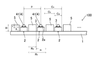
- a specific description will be given with reference to FIGS. 1A and 1B.
- the printed circuit board 100 includes a substrate 1 and a plurality of conductive joints 2 formed on the substrate 1.
- a core wire 41 of the coaxial cable 4 is connected to the upper surface (joint surface) 2 a of the conductive joint portion 2 by solder 3.
- Solder resist portions 5 are formed on both the left and right sides of the conductive joint portion 2.
- the conductive joints 2 are arranged at a predetermined pitch.
- the upper surface 2 a of the conductive joint portion 2 is a joint surface to which the core wire 41 of the coaxial cable 4 is joined.
- Solder 3 is applied to the entire upper surface 2a.
- the conductive joint portion 2 extends in a straight line in the vertical direction.
- the width Cw of the conductive joint 2 is, for example, 50 ⁇ m to 200 ⁇ m
- the pitch Cp of the conductive joint 2 is, for example, 100 ⁇ m to 400 ⁇ m.
- the core wire 41 can be satisfactorily connected to the conductive joint 2 by setting the conductive joint 2 to the above width.
- a fillet can be made into a favorable shape by arranging the electroconductive joining part 2 at the said pitch. Thereby, the connection strength between the conductive joint portion 2 and the core wire 41 can be maintained at a predetermined strength.
- the pitch Cp of the conductive joint 2 is the sum of the width Cw of the conductive joint 2 and the space Cs of the conductive joint 2.
- the space Cs of the conductive joint portion 2 is an interval between the two conductive joint portions 2 sandwiching the solder resist portion 5.
- the conductive joint 2 is formed by etching the substrate 1 or the like.
- the conductive joint portion 2 may be formed by printing a conductive material such as silver or copper on the substrate 1 and then firing it.
- the coaxial cable 4 includes a cylindrical core wire 41, an internal insulator 42 covering the core wire 41, an external conductor 43 covering the internal insulator 42, and an external insulator 44 in the outermost layer. is doing.
- the side peripheral surface of the core wire 41 particularly the lower half surface, is joined to the upper surface 2a of the conductive joint 2 by the solder 3 (see FIG. 1A).
- the upper half surface of the core wire 41 is exposed.
- a conductor member having a diameter of 15 ⁇ m or more and 100 ⁇ m or less can be used for the core wire 41.
- the pitch p of the core wire 41 is not less than 100 ⁇ m and not more than 400 ⁇ m, for example.
- solder resist portion 5 protrudes from the upper surface of the substrate 1 and is higher than the upper surface (bonding surface) 2 a of the conductive bonding portion 2.
- the protrusion length H of the solder resist portion 5 is longer than the sum of the height (thickness) h of the conductive joint portion 2 and the radius r of the core wire 41 (H> h + r).
- the “projection length H of the solder resist portion 5” is a length from the upper surface of the substrate 1 to the apex on the projection side of the solder resist portion 5.
- the solder resist portion 5 extends in a straight line parallel to the vertical direction.
- the distance (space) between the two solder resist portions 5 and 5 sandwiching the conductive joint portion 2 is the same length (width) w 1 at any position in the longitudinal direction (see FIGS. 1A and 1B).
- the width Rw of the solder resist portion 5 is, for example, 50 ⁇ m or more and 200 ⁇ m or less, and the pitch Rp of the solder resist portion 5 is, for example, 100 ⁇ m or more and 400 ⁇ m or less.
- the pitch Rp of the solder resist portion 5 is the sum of the width Rw of the solder resist portion 5 and the space w 1 of the solder resist portions 5 and 5.
- the solder resist portion 5 is formed by etching the substrate 1 or the like. At this time, it is preferable that the width Rw of the solder resist portion 5 is 50 ⁇ m or more and 200 ⁇ m or less, and the space w 1 is 50 ⁇ m or more and 200 ⁇ m or less.
- the width Rw and the space w 1 of the solder resist portion 5 can be adjusted by changing the light diameter at the time of UV irradiation, the light distribution, the irradiation position, the irradiation time, the light intensity, and the like. Further, it is also possible to adjust the width Rw and space w 1 of the solder resist portion 5 by adjusting the pattern width during etching of the substrate 1.
- the width Rw of the solder resist portion 5 is more preferably 60 ⁇ m or more and 120 ⁇ m or less, and more preferably 100 ⁇ m or more and 120 ⁇ m or less.
- the space w 1 of the solder resist portion 5 is more preferably 40 ⁇ m or more and 80 ⁇ m or less. With such a width Rw and space w 1, since it is possible to increase the contact area between the bottom and the substrate 1 of the solder resist section 5, the solder resist section 5 is less likely to peel off from the substrate 1.
- the core wire 41 is accommodated between the two solder resist portions 5 and 5, and the core wire 41 is placed on the upper surface 2a of the conductive joint portion 2 (conductor member setting step). Even if the core wire 41 is deformed and spreads in the width direction, the core wire 41 can be positioned on the upper surface 2 a of the conductive joint portion 2 by accommodating the core wire 41 between the two solder resist portions 5, 5. Solder 3 is applied in advance to the upper surface (bonding surface) 2 a of the conductive bonding portion 2.
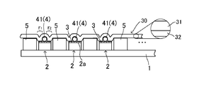
- the conductive joint 2, the solder 3, and the core wire 41 are covered with a light transmissive sheet 30 (see FIG. 2B).
- the core wire 41 is brought into contact with the solder 3.
- the core wire 41 and the solder 3 are covered with the light transmissive sheet 30 so that the core wire 41 is not deformed or moved.
- the upper half of the side peripheral surface of the core wire 41 is covered with the light transmissive sheet 30.
- the regions r 1 and r 2 on both sides of the core wire 41 are covered with the light transmissive sheet 30.
- the light transmissive sheet 30 includes a resin layer 31 formed of polyimide and an adhesive layer 32 formed below the resin layer 31 (see an enlarged view of FIG. 2B).
- the light transmissive sheet 30 is bonded to the core wire 41 and the solder 3 by the adhesive layer 32.
- the core wire 41 of the coaxial cable 4 is thin and lightweight, it is difficult to come into contact with the conductive joint portion 2 due to its own weight. Further, the core wire 41 is likely to move or deform to be in a non-contact state with the conductive joint portion 2. However, the core wire 41 is accommodated between the two solder resist portions 5, 5 and positioned on the upper surface 2 a of the conductive joint portion 2, and covered with the light transmissive sheet 30, whereby the core wire 41 is covered with the conductive joint portion 2. It can hold
- the core wire 41 is thin and lightweight, it moves and deforms to the left and right, and is likely to be in a non-contact state with the conductive joint portion 2. Further, the upper surface 2a of the conductive joint portion 2 is likely to rise in a curved shape. If the cylindrical core wire 41 is placed here and a light transmissive member is placed thereon, the core wire 41 is moved or deformed. Therefore, in this embodiment, the core wire 41 is placed on the conductive joint portion 2 by covering the core wire 41, the solder 3 (regions r 1 , r 2 ), and the conductive joint portion 2 with the light transmissive sheet 30. The movement and deformation of the core wire 41 can be suppressed while maintaining the state.
- light is applied to the light transmissive sheet 30 (see FIG. 2C).
- the light passes through the light transmissive sheet 30 and is applied to the solder 3 and the core wire 41, and the solder 3 is melted by light energy. Further, the energy of the light applied to the core wire 41 propagates to the solder 3 below the core wire 41 and melts the solder 3. Thereby, the electroconductive joining part 2 and the core wire 41 are joined by the solder 3 (joining process). For example, laser or infrared light may be irradiated as light. Thereafter, when the light transmissive sheet 30 is removed (see FIG. 2D), the connection structure of the present embodiment is obtained (light transmissive sheet removing step).
- the side peripheral surface of the lower half of the core wire 41 is soldered to the conductive joint 2.
- the side peripheral surface of the upper half of the core wire 41 may be exposed, and a part (adhesive) of the adhesive layer 32 of the light transmissive sheet 30 may partially remain and be laminated.
- the coaxial cable connection structure of the present embodiment has the following effects.
- the core wire 41 of the coaxial cable 4 becomes thinner, it is easy to spread in the width direction because it is light and easily deformed.
- the solder resist portions 5, 5 protrude on both sides of the upper surface 2a of the conductive bonding portion 2. Therefore, in a state where the core wire 41 is accommodated between the solder resist portions 5 and 5, the core wire 41 can be positioned and placed with respect to the upper surface 2a.
- the core wire 41 of the coaxial cable 4 that is easily deformed can be easily solder-connected to the upper surface 2 a of the conductive joint portion 2.
- solder joining can be performed mechanically instead of manual work. This improves workability.
- the core wire 41 is vibrated in a state where it is placed on the upper surface 2a of the conductive joint 2. Even when an external force such as air flow is applied, there is no concern that the core wire 41 gets over the solder resist portion 5. Therefore, the problem that the positioning of the core wire 41 is eliminated hardly occurs.
- the conductive solder 2 is heated and melted by irradiating light while holding the mounting state of the core wire 41 on the conductive joint 2 with the light transmissive sheet 30, thereby conducting the conductive joint 2. And the core wire 41 is joined. Thereby, even if the core wire 41 becomes thin and easily moved or deformed, the core wire 41 is prevented from moving or deformed by being covered with the light-transmitting sheet 30, and the core wire 41 is brought into contact with the conductive joint portion 2. Can do. For this reason, the core wire 41 can be bonded to the conductive bonding portion 2 with a high yield.
- the soldering iron is manually applied from above the core wire 41 as conventionally. It is possible to make it harder to form a solder bridge between the conductive joints 2 than in the case where the soldering operation is performed using the. As a result, a short circuit caused by the solder bridge can be made difficult to occur. In particular, when the pitch between the conductive joints 2 is narrowed, it is possible to significantly reduce the frequency of occurrence of bridges.
- a resin layer 31 formed of a polyimide resin is used for the light transmissive sheet 30. Since the polyimide resin can maintain the strength at the melting temperature when the preliminary solder is dissolved, the placement state of the core wire 41 can be maintained until the solder bonding is completed.
- the solder resist portion 205 is formed to be tapered as it approaches the apex (upper end) on the protruding side. On both side surfaces of the solder resist portion 205, tapered portions 205a and 205b that are inclined so as to approach the other side surface as they approach the apex are formed. The tapered portions 205a and 205b are planar.
- the distance (space) between the two solder resist portions 205 and 205 sandwiching the conductive joint portion 2 becomes wider as it approaches the apex.
- the vertex of the solder resist portion 205 205 (the upper end) and these intervals (spaces) are widest w 21, the lower end of the solder resist 205 is narrowest width w 1, the width w 21 than the width w 1 large.
- the core wire 41 of the coaxial cable 4 that is easily deformed or moved can be easily soldered to the upper surface (joint surface) 2 a of the conductive joint portion 2. Further, since the interval (space) between the two solder resist portions 205 and 205 sandwiching the conductive joint portion 2 is the widest at the apex, the core wire 41 extending to the width w 21 is accommodated between the solder resist portions 205 and 205. It can be connected to the upper surface 2 a of the conductive joint 2. Therefore, workability and yield can be improved.
- FIGS. 4A and 4B a third embodiment of the present invention will be described with reference to FIGS. 4A and 4B.
- the third embodiment differs from the first embodiment in the configuration of the solder resist portion.
- symbol is used and the description is abbreviate
- the solder resist portion 305 is formed in a trapezoidal shape whose width becomes narrower as it goes away from one end in the longitudinal direction near the base end of the core wire 41 in plan view (see FIG. 4B). Thereby, the space
- the distance (space) between the solder resist portions 305 and 305 is the narrowest distance (space) w 1 at one end in the longitudinal direction near the fixed end (base end) of the core wire 41 and the other end in the longitudinal direction closest to the tip of the core wire 41. Is the widest distance (space) w 31 , and the distance (space) w 31 is shorter than the distance (space) w 1 .
- the core wire 41 of the coaxial cable 4 that is easily deformed or moved can be easily soldered to the upper surface (joint surface) 2 a of the conductive joint portion 2. Further, the core wire 41 is likely to be deformed and spread in the width direction as it moves away from the fixed end (the upper end portion in FIG. 4B). However, in the above configuration, the distance between the solder resist portion 305, 305 (space) is wide as the distance from the fixed end of the core wire 41, extends to the maximum width w 31 at the tip of the core wire 41.
- the core wire 41 can be accommodated between the solder resist portions 305 and 305 and connected to the upper surface 2 a of the conductive joint portion 2. Therefore, workability and yield can be improved.
- FIGS. 5A and 5B a fourth embodiment of the present invention will be described with reference to FIGS. 5A and 5B.
- the fourth embodiment is different from the first embodiment in the configuration of the solder resist portion.
- symbol is used and the description is abbreviate
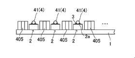
- the solder resist portion 405 has both side surfaces 405a and 405b curved outwardly (see FIG. 5B) and is widest in the vicinity of the center in the longitudinal direction.
- the interval (space) between the two solder resist portions 405 and 405 sandwiching the conductive joint portion 2 is the narrowest in the vicinity of the center in the longitudinal direction and becomes wider as the distance from the center increases.
- the distance (space) between the two solder resist portions 405 and 405 is the narrowest distance (space) w 41 in the vicinity of the center in the longitudinal direction of the solder resist portion 405, and one end portion in the longitudinal direction of the solder resist portion 405 and the like. It is the widest (space) distance w 42 at the end, and the distance w 41 is shorter than the distance w 42 .
- the core wire 41 of the coaxial cable 4 that is easily deformed or moved can be easily soldered to the upper surface (joint surface) 2 a of the conductive joint portion 2. Moreover, the core wire 41 is easily deformed as it goes away from the fixed end (the upper end portion in FIG. 5B), and easily spreads in the width direction.
- the distance (space) between the solder resist portions 405 and 405 increases as the distance from the fixed end of the core wire 41 increases, and extends to the maximum width w 41 at the tip of the core wire 41.
- the core wire 41 can be accommodated between the solder resist portions 505 and 305 and connected to the upper surface 2 a of the conductive joint portion 2. Further, since the distance (space) between the solder resist portions 405 and 405 is wide at both ends in the longitudinal direction, it is determined whether the position where the core wire 41 is wide is the front end side (fixed end side) or the base end side. The core wire 41 can be accommodated in an inclined state from the distal end side or the proximal end side. Thereby, workability
- a conductive member and a solder resist were formed by etching the substrate to obtain the structure shown in FIGS. 1A and 1B (state without solder and core material). And the ease of peeling of a soldering resist was evaluated based on the following item.
- ⁇ is less peelable than ⁇ , but ⁇ and ⁇ can be used without any problem.
- Table 1 shows experimental conditions and evaluation results.
- the width Cw and space Cs of the conductive member and the widths Rw and w 1 of the solder resist were adjusted by adjusting the irradiation width of light (ultraviolet light was used in this experiment) during etching of the substrate.
- the irradiation width of light was set to 50 ⁇ m or less.
- the light irradiation width was set to 60 ⁇ m, and in Experiment Nos. 4 to 6, the light irradiation width was set to 100 ⁇ m or more. In Experiment No. 6, the irradiation width of light is set to 120 ⁇ m or more.
- the second to fourth embodiments and the modifications described later have different solder resist shapes from the first embodiment, but the difference in these shapes has little to do with the ease of peeling of the solder resist from the substrate. Therefore, also in the second to fourth embodiments and the modified examples, by making the width and space similar to those in Experiments Nos. 3 to 6, a structure in which the solder resist is difficult to peel can be obtained.
- the tapered portions 205a and 205b are formed on both side surfaces of the solder resist portion 205, respectively, but the tapered portions may be formed only on one side surface. Thereby, the number of processing steps of the solder resist portion 205 can be reduced while the distance (space) between the two solder resist portions 205 and 205 sandwiching the conductive joint portion 2 is increased.
- the tapered portions 205a and 205b formed in the solder resist portion 205 are planar, but the tapered portions may be curved in a convex shape or a concave shape.
- the tapered portions 205a and 205b are formed in the entire longitudinal direction of the solder resist portion 205, but the tapered portion may be formed in a part of the longitudinal direction of the solder resist portion.
- the distance (space) between the two solder resist portions 405 and 405 sandwiching the conductive joint portion 2 is the shortest in the vicinity of the center in the longitudinal direction and becomes wider as it approaches both ends in the longitudinal direction.
- the distance between the two solder resist portions 405 and 405 sandwiching the conductive joint portion 2 may be longest in the vicinity of the center in the longitudinal direction and narrower as it approaches both ends in the longitudinal direction.
- solder resist portions formed on one printed circuit board have the same shape, but solder resist portions having different shapes may be used.
- polyimide resin is used for the resin layer of the light transmissive sheet in the printed circuit board manufacturing process, but other resins may be used as long as the melting point is higher than that of solder.
- the solder is entirely applied to the upper surface of the conductive joint portion 2, but the solder may be applied to a part of the upper surface of the conductive connection member.
- the light transmissive sheet 30 is attached to the substantially upper half of the central conductor 21, the exposed portion of the solder 3, and the exposed portion of the upper surface of the conductive joint portion 2. .
- the height of the solder resist portion is constant, but the height of the solder resist portion may be changed.
- the protruding height of the solder resist portion 505 may be increased as the distance from the base end of the core wire 41 (the right side in FIG. 6B) increases.
- the protrusion length of the solder resist portion 505 is the lowest protrusion length h 51 at one end in the longitudinal direction near the base end of the core wire 41 and the longest protrusion length h 52 at the other end in the longitudinal direction near the distal end of the core wire 41.
- the length h 51 is shorter than the protrusion length h 52 .
- the protruding length h 51 and the protruding length h 52 are both longer than the sum of the height of the conductive joint 2 and the radius of the core wire 41. Even in such a configuration, the effect of the present invention can be obtained. Further, the core wire 41 is likely to be deformed and spread in the width direction and the height direction as it moves away from the fixed end (left end portion in FIG. 6B). For this reason, when an external force such as vibration or airflow is generated in a state where the core wire 41 is accommodated between the solder resist portions 505 and 505, the tip end portion (the right end portion in FIG. 6B) of the core wire 41 easily gets over the solder resist portion 505.
- the height of the solder resist portion is changed in the first embodiment.
- the height of the solder resist portion is changed as shown in FIGS. 6A and 6B. May be.
Landscapes
- Engineering & Computer Science (AREA)
- Manufacturing & Machinery (AREA)
- Microelectronics & Electronic Packaging (AREA)
- Coupling Device And Connection With Printed Circuit (AREA)
- Connections Effected By Soldering, Adhesion, Or Permanent Deformation (AREA)
- Electric Connection Of Electric Components To Printed Circuits (AREA)
- Structures For Mounting Electric Components On Printed Circuit Boards (AREA)
- Insulated Conductors (AREA)
- Multi-Conductor Connections (AREA)
- Insertion, Bundling And Securing Of Wires For Electric Apparatuses (AREA)
Priority Applications (3)
| Application Number | Priority Date | Filing Date | Title |
|---|---|---|---|
| KR1020177007462A KR101937281B1 (ko) | 2014-10-29 | 2015-10-29 | 동축 케이블의 접속 구조 |
| CN201580059173.3A CN107112641B (zh) | 2014-10-29 | 2015-10-29 | 同轴缆线的连接构造 |
| US15/521,801 US9806434B2 (en) | 2014-10-29 | 2015-10-29 | Coaxial cable connection structure |
Applications Claiming Priority (2)
| Application Number | Priority Date | Filing Date | Title |
|---|---|---|---|
| JP2014220864A JP6193835B2 (ja) | 2014-10-29 | 2014-10-29 | 同軸ケーブルの接続構造 |
| JP2014-220864 | 2014-10-29 |
Publications (1)
| Publication Number | Publication Date |
|---|---|
| WO2016068259A1 true WO2016068259A1 (ja) | 2016-05-06 |
Family
ID=55857594
Family Applications (1)
| Application Number | Title | Priority Date | Filing Date |
|---|---|---|---|
| PCT/JP2015/080614 Ceased WO2016068259A1 (ja) | 2014-10-29 | 2015-10-29 | 同軸ケーブルの接続構造 |
Country Status (6)
| Country | Link |
|---|---|
| US (1) | US9806434B2 (https=) |
| JP (1) | JP6193835B2 (https=) |
| KR (1) | KR101937281B1 (https=) |
| CN (1) | CN107112641B (https=) |
| TW (1) | TWI616040B (https=) |
| WO (1) | WO2016068259A1 (https=) |
Families Citing this family (1)
| Publication number | Priority date | Publication date | Assignee | Title |
|---|---|---|---|---|
| JP7234188B2 (ja) * | 2020-07-22 | 2023-03-07 | 矢崎総業株式会社 | 電線の製造方法および電線製造装置 |
Citations (3)
| Publication number | Priority date | Publication date | Assignee | Title |
|---|---|---|---|---|
| JPH10112580A (ja) * | 1996-10-08 | 1998-04-28 | Sony Corp | プリント配線基板 |
| JP2012174484A (ja) * | 2011-02-22 | 2012-09-10 | Olympus Corp | ケーブル接続構造およびケーブル接続方法 |
| JP2014089902A (ja) * | 2012-10-31 | 2014-05-15 | Hitachi Metals Ltd | ケーブル接続体およびケーブル接続方法 |
Family Cites Families (6)
| Publication number | Priority date | Publication date | Assignee | Title |
|---|---|---|---|---|
| US5139448A (en) * | 1985-05-24 | 1992-08-18 | North American Specialties Corporation | Solder-bearing lead |
| US5797765A (en) * | 1996-11-01 | 1998-08-25 | Hewlett-Packard Company | Coaxial connector for mounting on a circuit substrate |
| CN1216420C (zh) * | 2001-12-14 | 2005-08-24 | 矽品精密工业股份有限公司 | 可设置无源元件的芯片承载件 |
| JP5510090B2 (ja) * | 2010-06-10 | 2014-06-04 | 日立金属株式会社 | ケーブル接続構造、及びケーブル接続方法 |
| JP5479432B2 (ja) | 2011-10-24 | 2014-04-23 | 株式会社フジクラ | ケーブルアッセンブリ |
| CN202737148U (zh) * | 2012-07-10 | 2013-02-13 | 贝尔威勒电子股份有限公司 | 缆线连接器的端子焊接结构 |
-
2014
- 2014-10-29 JP JP2014220864A patent/JP6193835B2/ja active Active
-
2015
- 2015-10-29 WO PCT/JP2015/080614 patent/WO2016068259A1/ja not_active Ceased
- 2015-10-29 US US15/521,801 patent/US9806434B2/en active Active
- 2015-10-29 TW TW104135651A patent/TWI616040B/zh active
- 2015-10-29 CN CN201580059173.3A patent/CN107112641B/zh active Active
- 2015-10-29 KR KR1020177007462A patent/KR101937281B1/ko active Active
Patent Citations (3)
| Publication number | Priority date | Publication date | Assignee | Title |
|---|---|---|---|---|
| JPH10112580A (ja) * | 1996-10-08 | 1998-04-28 | Sony Corp | プリント配線基板 |
| JP2012174484A (ja) * | 2011-02-22 | 2012-09-10 | Olympus Corp | ケーブル接続構造およびケーブル接続方法 |
| JP2014089902A (ja) * | 2012-10-31 | 2014-05-15 | Hitachi Metals Ltd | ケーブル接続体およびケーブル接続方法 |
Also Published As
| Publication number | Publication date |
|---|---|
| JP6193835B2 (ja) | 2017-09-06 |
| TWI616040B (zh) | 2018-02-21 |
| CN107112641A (zh) | 2017-08-29 |
| JP2016091610A (ja) | 2016-05-23 |
| TW201626641A (zh) | 2016-07-16 |
| US9806434B2 (en) | 2017-10-31 |
| KR20170074854A (ko) | 2017-06-30 |
| KR101937281B1 (ko) | 2019-01-10 |
| CN107112641B (zh) | 2019-03-29 |
| US20170250476A1 (en) | 2017-08-31 |
Similar Documents
| Publication | Publication Date | Title |
|---|---|---|
| JP6581861B2 (ja) | 電子部品搭載用基板の製造方法 | |
| CN103367302A (zh) | 基板装置 | |
| TWI674821B (zh) | 板體集積式互連體裝置及其形成方法 | |
| CN111919520A (zh) | 电子电路装置以及电路基板的制造方法 | |
| JP6570728B2 (ja) | 電子装置およびその製造方法 | |
| JP6193835B2 (ja) | 同軸ケーブルの接続構造 | |
| JP5854449B2 (ja) | 電子回路基板 | |
| TWI630767B (zh) | 印刷基板之製造方法及導電性構件之接合方法 | |
| JP2010212320A (ja) | フレキシブルプリント配線板 | |
| JP2016082074A (ja) | 電装装置およびその製造方法 | |
| JP2006165079A (ja) | フレキシブルプリント基板 | |
| WO2017138381A1 (ja) | フレキシブルケーブル付電子部品連およびフレキシブルケーブル付電子部品連の製造方法 | |
| CN110913575B (zh) | 面板、pcb以及pcb的制造方法 | |
| JP6982755B2 (ja) | プリント回路基板及びプリント回路装置 | |
| TWM640310U (zh) | 連接器結構 | |
| JP2018190790A (ja) | フレキシブル配線の接合装置、及び回路の製造方法 | |
| JP2007109970A (ja) | プリント配線板及びその接続構造 | |
| JP2001059911A (ja) | 光ファイバ実装用プリント配線板およびプリント配線板の製造方法 | |
| TW201440583A (zh) | 具有對應焊墊結構設計之線路板 | |
| JP2010023067A (ja) | 半田付け方法 | |
| JP2008060404A (ja) | フレキシブル配線基板およびフレキシブル配線基板の作製方法 | |
| JP2006128525A (ja) | フレキシブル基板 | |
| JP2019186385A (ja) | 実装構造体 | |
| JP2007149888A (ja) | プリント配線板、プリント配線板の接続構造、及びプリント配線板間接続部の封止方法 | |
| JP2017224647A (ja) | 回路基板の製造方法 |
Legal Events
| Date | Code | Title | Description |
|---|---|---|---|
| 121 | Ep: the epo has been informed by wipo that ep was designated in this application |
Ref document number: 15854452 Country of ref document: EP Kind code of ref document: A1 |
|
| ENP | Entry into the national phase |
Ref document number: 20177007462 Country of ref document: KR Kind code of ref document: A |
|
| WWE | Wipo information: entry into national phase |
Ref document number: 15521801 Country of ref document: US |
|
| NENP | Non-entry into the national phase |
Ref country code: DE |
|
| 122 | Ep: pct application non-entry in european phase |
Ref document number: 15854452 Country of ref document: EP Kind code of ref document: A1 |