WO2016067518A1 - 研磨装置 - Google Patents
研磨装置 Download PDFInfo
- Publication number
- WO2016067518A1 WO2016067518A1 PCT/JP2015/004842 JP2015004842W WO2016067518A1 WO 2016067518 A1 WO2016067518 A1 WO 2016067518A1 JP 2015004842 W JP2015004842 W JP 2015004842W WO 2016067518 A1 WO2016067518 A1 WO 2016067518A1
- Authority
- WO
- WIPO (PCT)
- Prior art keywords
- wafer
- polishing
- surface plate
- polishing head
- detection sensor
- Prior art date
Links
- 238000005498 polishing Methods 0.000 title claims abstract description 200
- 238000001514 detection method Methods 0.000 claims abstract description 61
- 239000004744 fabric Substances 0.000 claims abstract description 16
- 230000002093 peripheral effect Effects 0.000 claims description 7
- 238000011144 upstream manufacturing Methods 0.000 claims description 5
- 235000012431 wafers Nutrition 0.000 abstract description 172
- 230000000052 comparative effect Effects 0.000 description 17
- 230000009191 jumping Effects 0.000 description 14
- 239000003638 chemical reducing agent Substances 0.000 description 9
- 238000000034 method Methods 0.000 description 4
- 239000003795 chemical substances by application Substances 0.000 description 3
- 230000005856 abnormality Effects 0.000 description 2
- 239000003082 abrasive agent Substances 0.000 description 2
- 238000005336 cracking Methods 0.000 description 2
- 239000012634 fragment Substances 0.000 description 2
- 239000013307 optical fiber Substances 0.000 description 2
- XUIMIQQOPSSXEZ-UHFFFAOYSA-N Silicon Chemical compound [Si] XUIMIQQOPSSXEZ-UHFFFAOYSA-N 0.000 description 1
- 230000005540 biological transmission Effects 0.000 description 1
- 230000002542 deteriorative effect Effects 0.000 description 1
- 230000000694 effects Effects 0.000 description 1
- 238000005259 measurement Methods 0.000 description 1
- 239000004745 nonwoven fabric Substances 0.000 description 1
- 238000007517 polishing process Methods 0.000 description 1
- 229910052710 silicon Inorganic materials 0.000 description 1
- 239000010703 silicon Substances 0.000 description 1
- 238000001179 sorption measurement Methods 0.000 description 1
- XLYOFNOQVPJJNP-UHFFFAOYSA-N water Substances O XLYOFNOQVPJJNP-UHFFFAOYSA-N 0.000 description 1
Images

Classifications
-
- B—PERFORMING OPERATIONS; TRANSPORTING
- B24—GRINDING; POLISHING
- B24B—MACHINES, DEVICES, OR PROCESSES FOR GRINDING OR POLISHING; DRESSING OR CONDITIONING OF ABRADING SURFACES; FEEDING OF GRINDING, POLISHING, OR LAPPING AGENTS
- B24B37/00—Lapping machines or devices; Accessories
- B24B37/005—Control means for lapping machines or devices
- B24B37/0053—Control means for lapping machines or devices detecting loss or breakage of a workpiece during lapping
-
- B—PERFORMING OPERATIONS; TRANSPORTING
- B24—GRINDING; POLISHING
- B24B—MACHINES, DEVICES, OR PROCESSES FOR GRINDING OR POLISHING; DRESSING OR CONDITIONING OF ABRADING SURFACES; FEEDING OF GRINDING, POLISHING, OR LAPPING AGENTS
- B24B37/00—Lapping machines or devices; Accessories
- B24B37/04—Lapping machines or devices; Accessories designed for working plane surfaces
- B24B37/07—Lapping machines or devices; Accessories designed for working plane surfaces characterised by the movement of the work or lapping tool
- B24B37/10—Lapping machines or devices; Accessories designed for working plane surfaces characterised by the movement of the work or lapping tool for single side lapping
-
- B—PERFORMING OPERATIONS; TRANSPORTING
- B24—GRINDING; POLISHING
- B24B—MACHINES, DEVICES, OR PROCESSES FOR GRINDING OR POLISHING; DRESSING OR CONDITIONING OF ABRADING SURFACES; FEEDING OF GRINDING, POLISHING, OR LAPPING AGENTS
- B24B37/00—Lapping machines or devices; Accessories
- B24B37/34—Accessories
-
- B—PERFORMING OPERATIONS; TRANSPORTING
- B24—GRINDING; POLISHING
- B24B—MACHINES, DEVICES, OR PROCESSES FOR GRINDING OR POLISHING; DRESSING OR CONDITIONING OF ABRADING SURFACES; FEEDING OF GRINDING, POLISHING, OR LAPPING AGENTS
- B24B49/00—Measuring or gauging equipment for controlling the feed movement of the grinding tool or work; Arrangements of indicating or measuring equipment, e.g. for indicating the start of the grinding operation
- B24B49/12—Measuring or gauging equipment for controlling the feed movement of the grinding tool or work; Arrangements of indicating or measuring equipment, e.g. for indicating the start of the grinding operation involving optical means
-
- B—PERFORMING OPERATIONS; TRANSPORTING
- B24—GRINDING; POLISHING
- B24B—MACHINES, DEVICES, OR PROCESSES FOR GRINDING OR POLISHING; DRESSING OR CONDITIONING OF ABRADING SURFACES; FEEDING OF GRINDING, POLISHING, OR LAPPING AGENTS
- B24B7/00—Machines or devices designed for grinding plane surfaces on work, including polishing plane glass surfaces; Accessories therefor
- B24B7/20—Machines or devices designed for grinding plane surfaces on work, including polishing plane glass surfaces; Accessories therefor characterised by a special design with respect to properties of the material of non-metallic articles to be ground
- B24B7/22—Machines or devices designed for grinding plane surfaces on work, including polishing plane glass surfaces; Accessories therefor characterised by a special design with respect to properties of the material of non-metallic articles to be ground for grinding inorganic material, e.g. stone, ceramics, porcelain
- B24B7/228—Machines or devices designed for grinding plane surfaces on work, including polishing plane glass surfaces; Accessories therefor characterised by a special design with respect to properties of the material of non-metallic articles to be ground for grinding inorganic material, e.g. stone, ceramics, porcelain for grinding thin, brittle parts, e.g. semiconductors, wafers
-
- H—ELECTRICITY
- H01—ELECTRIC ELEMENTS
- H01L—SEMICONDUCTOR DEVICES NOT COVERED BY CLASS H10
- H01L21/00—Processes or apparatus adapted for the manufacture or treatment of semiconductor or solid state devices or of parts thereof
- H01L21/02—Manufacture or treatment of semiconductor devices or of parts thereof
- H01L21/04—Manufacture or treatment of semiconductor devices or of parts thereof the devices having potential barriers, e.g. a PN junction, depletion layer or carrier concentration layer
- H01L21/18—Manufacture or treatment of semiconductor devices or of parts thereof the devices having potential barriers, e.g. a PN junction, depletion layer or carrier concentration layer the devices having semiconductor bodies comprising elements of Group IV of the Periodic Table or AIIIBV compounds with or without impurities, e.g. doping materials
- H01L21/30—Treatment of semiconductor bodies using processes or apparatus not provided for in groups H01L21/20 - H01L21/26
- H01L21/302—Treatment of semiconductor bodies using processes or apparatus not provided for in groups H01L21/20 - H01L21/26 to change their surface-physical characteristics or shape, e.g. etching, polishing, cutting
- H01L21/304—Mechanical treatment, e.g. grinding, polishing, cutting
Definitions
- the present invention relates to a polishing apparatus, and more particularly to a polishing apparatus including a wafer detection sensor.
- Polishing of one side of a wafer is performed using a polishing apparatus composed of a surface plate to which a polishing cloth is attached, an abrasive supply mechanism for supplying an abrasive onto the polishing cloth, and a polishing head for holding the wafer. Is called.
- the wafer is held by the polishing head, and the polishing agent is supplied onto the polishing cloth from the polishing agent supply mechanism, and the wafer is polished by sliding the surface of the wafer against the polishing cloth while rotating the surface plate and the polishing head, respectively.
- a polishing apparatus composed of a surface plate to which a polishing cloth is attached, an abrasive supply mechanism for supplying an abrasive onto the polishing cloth, and a polishing head for holding the wafer.
- the wafer is held by the polishing head, and the polishing agent is supplied onto the polishing cloth from the polishing agent supply mechanism, and the wafer is polished by sliding the surface of the wafer against the polishing cloth while rotating the surface plate and
- the wafer When a wafer is being polished by the above polishing apparatus, the wafer may jump out of the polishing head. Also, due to a pickup mistake, the wafer after polishing may be left on the surface plate. In order to detect these, a wafer detection sensor is attached to the polishing apparatus.
- the wafer detection sensor When the wafer detection sensor detects that the wafer has jumped out of the polishing head during polishing, it can prevent the protruding wafer from contacting other polishing heads and cracking, or continue polishing when the wafer is cracked. In order to prevent this, a function of stopping the polishing apparatus and issuing an alarm to notify the operator of an abnormality is also added.
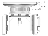
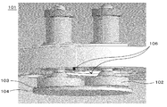
- the wafer detection sensor was installed at two locations in the middle of the adjacent polishing head 102 at the upper part of the surface plate 104.
- the wafer detection sensor 106 is an optical fiber type and uses a general object having a time of 500 ⁇ s from when a wafer is detected to when a stop signal is output.
- a worm speed reducer 111 and a constant torque motor 112 for driving an inverter as shown in FIG. 11 have been used.
- the rotation of the inverter driving constant torque motor 112 is transmitted to the speed reducer 111 by a pulley and a timing belt.
- the wafer detection sensor cannot detect a wafer that has jumped out of the polishing head 102, it may collide with another polishing head existing on the same surface plate and the wafer may be damaged.
- the polishing head moves to another surface plate and continues to polish, so it is normal for broken wafer fragments adhering to the polishing head.
- the polishing cloth 103 may be secondarily contaminated.
- polishing cloth 103 is cleaned or replaced. Further, the damaged wafer remains on the suction surface of the polishing head 102 and the retainer guide, and the polishing head 102 cannot be used, and the polishing head 102 is replaced.
- the wafer detection sensor 106 recognizes the wafer by light reflection when the wafer jumps out of the polishing head 102, and suddenly stops the rotation of the motor 112 of the surface plate drive mechanism.
- the platen drive mechanism has a power transmission part due to mechanical contact such as a speed reducer, which leads to damage to the equipment such as gear breakage, belt tooth jumping, and wear in the speed reducer. Can not stop immediately.
- the motor since the motor itself does not have a function that can be forcibly stopped, the motor continues to rotate with an inertia proportional to the weight of the surface plate 104. In such a case, the rotation of the surface plate 104 is stopped by the pressure of pressing the surface plate 104 with the polishing head 102.
- the wafer detection sensor detects that the wafer has jumped out of the polishing head during polishing and performs an operation to stop the surface plate. Wafer collision can be avoided.
- the rotation speed of the surface plate is high or medium, the surface plate will stop even if the wafer detection sensor detects that the wafer has jumped out of the polishing head during polishing and stops the surface plate.
- the wafer collides without being in time there is a problem that the wafer collides without being in time.
- the present invention has been made in view of the above-described problems, and provides a polishing apparatus capable of detecting earlier that a wafer has jumped out of a polishing head during polishing and preventing damage to the wafer. Objective.
- a plurality of polishing heads for holding a wafer, a rotatable surface plate to which a polishing cloth for polishing the wafer is attached, and the surface plate
- a polishing apparatus comprising a platen drive mechanism for rotating the wafer and a plurality of wafer detection sensors for detecting that the wafer has jumped out of the polishing head during polishing, Provided with the polishing apparatus, wherein the wafer detection sensor is provided on the downstream side in the rotation direction of the surface plate with respect to each of the polishing heads and above the periphery of the outer peripheral portion of the polishing head.
- the wafer detection sensor is provided on the upstream side in the rotation direction of the surface plate with respect to each of the polishing heads and above the periphery of the outer peripheral portion of the polishing head. If this is the case, even when the wafer is polished by rotating the rotation direction of the surface plate in the reverse direction to the above rotation, it is possible to detect earlier that the wafer has jumped out of the polishing head during polishing. . As a result, it is possible to prevent the wafer jumping out from the polishing head from colliding with another polishing head.
- the wafer detection sensor preferably has a time from detection of the wafer to output of a detection signal of 80 ⁇ s or less. In such a case, since the time from detection of the wafer to output of the detection signal is early, it is possible to more reliably prevent the wafer jumping out of the polishing head from colliding with another polishing head. it can.
- the surface plate drive mechanism is a device that directly rotates the surface plate by a motor without using a speed reducer, and has a function of forcibly stopping the rotation of the motor. In such a case, since the time until the rotation of the surface plate stops is fast, it is possible to more reliably prevent the wafer jumping out of the polishing head from colliding with another polishing head.
- the polishing apparatus of the present invention it is possible to detect earlier that the wafer has jumped out of the polishing head during polishing as compared with the prior art. As a result, the wafer jumping out from the polishing head can be prevented from colliding with another polishing head, and the wafer can be prevented from being damaged.
- the present invention is not limited to this.
- the wafer jumps out of the polishing head and collides with another polishing head, thereby causing damage to the wafer and deteriorating productivity.
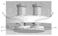
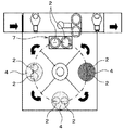
- a polishing apparatus 1 of the present invention includes a plurality of polishing heads 2 for holding a wafer, and a rotatable surface plate 4 to which a polishing cloth 3 for polishing the wafer is attached.
- a platen drive mechanism 5 (see FIG. 2) for rotating the platen 4 and a plurality of wafer detection sensors 6 for detecting that the wafer has jumped out of the polishing head 2 during polishing.
- the two polishing heads 2 are disposed above the surface plate 4.
- the wafer can be held by the polishing head 2 using any method.
- a vacuum adsorption method or a water filling method using a template can be used.
- a surface plate drive mechanism 5 is provided at the bottom of the surface plate 4. Then, while rotating the surface plate by the surface plate driving mechanism 5, the polishing head 2 holding the wafer is rotated while supplying the abrasive onto the surface plate 4 from the abrasive supply mechanism (not shown), and the wafer is moved. The wafer is polished by being brought into sliding contact with the polishing cloth 3.
- the wafer detection sensor 6 detects the wafer that has jumped out in this way. Further, the wafer detection sensor 6 can also detect forgetting to place a wafer due to a wafer pick-up mistake after completion of polishing.
- the wafer detection sensor 6 When the wafer detection sensor 6 detects that the wafer has jumped out of the polishing head 2 during polishing, the wafer detection sensor 6 outputs a detection signal (forced stop signal) to the surface plate driving mechanism 5 to stop the rotation of the surface plate 4. As a result, it is possible to prevent the protruding wafer from coming into contact with other polishing heads 2 and cracking, or from continuing polishing with the wafer being cracked. Further, the wafer detection sensor 6 can have a function of notifying the operator of an abnormality by stopping the polishing apparatus and issuing an alarm.
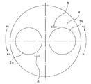
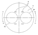
- the wafer detecting sensors 6, each of the polishing heads 2a, the rotation direction of the downstream side of the platen 4 with respect 2b (x 2 side) and provided above the periphery of the outer peripheral portion of the polishing head 2 It is what. In such a case, as described above, the wafer jumping out from the polishing head 2 moves in the rotation direction of the surface plate 4, so that it can be detected earlier that the wafer has jumped out from the polishing head 2. . As a result, it is possible to prevent the wafer jumping out from the polishing head 2 from colliding with another polishing head.
- the wafer detection sensor 6 further has an upstream side in the rotation direction of the surface plate 4 with respect to each polishing head 2a, 2b as shown in FIG. (x 1 side) and the polishing head 2a, it is preferable that also provided above the periphery of the outer peripheral portion of 2b.
- the wafer detection sensor 6 preferably has a fast time from detection of a wafer to output of a detection signal, preferably 80 ⁇ s or less.
- a reflective laser sensor can be used as the wafer detection sensor. If it is such, the abrasive
- the surface plate drive mechanism 5 directly rotates the surface plate 4 with a motor without using a speed reducer, and preferably has a function of forcibly stopping the rotation of the motor.
- a direct drive servomotor is preferably used. In such a case, since the time until the rotation of the surface plate stops is fast, it is possible to more reliably prevent the wafer jumping out of the polishing head from colliding with another polishing head. Further, it is possible to prevent damage to the surface plate drive mechanism 5 such as breakage of gears in the speed reducer, belt tooth skipping, and wear due to the forced stop of the surface plate 4.
- polishing apparatus of the present invention can be applied to an index type polishing apparatus as described above.
- the polishing apparatus includes a wafer detection sensor 6 at a position as shown in FIG. 4 and at a position separated from the surface plate 4 by 150 cm or more in the height direction.
- the wafer detection sensor 6 is a reflective laser sensor (LV-H32 manufactured by Keyence Corporation), and has a time from detection of a wafer to output of a detection signal of 80 ⁇ s.
- the surface plate driving mechanism directly rotates the surface plate 4 with a motor without using a speed reducer, and a direct drive servo motor having a function of forcibly stopping the rotation of the motor is used. .
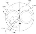
- the angle ⁇ 1 formed between the center of the wafer W and the straight line (b 1 ) passing through the center of the surface plate 4 when the wafer W is in contact with the adjacent polishing head 2 b was determined.
- This angle ⁇ 1 indicates a movement angle from the time when the protrusion of the wafer W is detected until the wafer W moves in the rotation direction of the surface plate 4 and finally contacts another polishing head. The larger the angle, the faster the detection, and the longer the allowable time from detection to stop of the surface plate.
- ⁇ 1 was 33.5 °.
- ⁇ 1 was a larger value than ⁇ 2 of Comparative Example 1 described later. That is, Example 1 was able to detect the wafers that jumped out of the polishing head earlier than Comparative Example 1.
- the wafer was polished using a conventional polishing apparatus in which wafer detection sensors 106 were provided in two places between adjacent polishing heads 102 a and 102 b and above the surface plate 104.
- the wafer detection sensor 106 is an optical fiber type, and a general object having a time of 500 ⁇ s from detection of a wafer to output of a detection signal is used.
- the surface plate driving mechanism one comprising a worm speed reducer 111 and a constant torque motor 112 for driving an inverter as shown in FIG. 11 was used.
- Example 2 Using the same polishing apparatus of the present invention as in Example 1, a wafer having a diameter of 300 mm was polished.
- the rotation speed of the surface plate 4 during polishing was changed from 10 rpm to 40 rpm.
- the time it takes for the surface plate to stop after the wafer detection sensor detects that the wafer has jumped out of the polishing head during polishing (the surface plate stop time) and the time it actually stops the surface plate
- Table 1 shows the angle of rotation of the surface plate (surface plate movement angle), along with the presence / absence of collision (crash) of the wafer with the polishing head, for each changed number of rotations of the surface plate 4.
- the measurement results of Comparative Example 2 described later are also shown.
- Example 2 Since a direct drive servomotor was used for the surface plate driving mechanism, as shown in Table 1, in Example 2, the surface plate stop time was 60 ms regardless of the surface plate rotation speed. The platen movement angle increased as the platen rotation speed was increased. When the platen rotation speed was 40 rpm, the platen movement angle was 14.4 °. Even when the rotation speed of the platen was 40 rpm, this angle was smaller than ⁇ 1 (33.5 °) obtained in Example 1, so that no crash due to the jumping out of the wafer occurred. On the other hand, as described later, in Comparative Example 2, a crash occurred when the rotation speed of the surface plate was 20 rpm or more.
- Comparative Example 2 In the same manner as in Example 2 except that the conventional polishing apparatus similar to Comparative Example 1 was used, during the polishing of a wafer having a diameter of 300 mm, the wafer detection sensor detected that the wafer had jumped out of the polishing head. The surface plate stop time and the surface plate movement angle were measured and are shown in Table 1 together with the presence or absence of a wafer crash.
- Example 3 As shown in FIG. 5, three surface plates 4 and a load / unload stage 7 are provided, and two polishing heads 2 are respectively assigned to the surface plate 4 and the load / unload stage 7.
- a wafer having a diameter of 300 mm was polished using such an index type polishing apparatus (SRED manufactured by Fujikoshi Machinery Co., Ltd.).
- a nonwoven fabric and a suede polishing cloth are affixed to the three surface plates 4.
- the wafer detection sensor and the surface plate drive mechanism were the same as in Example 1.
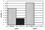
- the surface plate 4 and the polishing head 2 are rotated in the same rotational direction, the surface plate is 6.6 to 29.0 rpm, and the polishing head is 6.6 to 31 rpm. Polishing was performed with a load of 2 . The frequency at which the wafer jumped out from the polishing head 2 during polishing was measured. Further, the frequency of occurrence of wafer crash due to the jumping out of the wafer was measured, and these are shown in FIG.
- the frequency of occurrence of wafer pop-out from the polishing head 2 during polishing was 0.092%, which was the same level as Comparative Example 3 described later.
- the frequency of occurrence of wafer crash was 0%, and no wafer crash occurred in Example 3.
- Comparative Example 3 a wafer crash occurred.
- the wafer productivity was higher than that in Comparative Example 3.
- Comparative Example 3 During the polishing of a wafer having a diameter of 300 mm in the same manner as in Example 3 except that the wafer was polished using the index type polishing apparatus having the configuration of the wafer detection sensor and the surface plate driving mechanism as in Comparative Example 1. The frequency at which the wafer jumped out and the frequency at which the wafer crash occurred were measured, and these are shown in FIG. 8 and Table 2.
- the present invention is not limited to the above embodiment.
- the above-described embodiment is an exemplification, and the present invention has any configuration that has substantially the same configuration as the technical idea described in the claims of the present invention and that exhibits the same effects. Are included in the technical scope.
Landscapes
- Engineering & Computer Science (AREA)
- Mechanical Engineering (AREA)
- Physics & Mathematics (AREA)
- Condensed Matter Physics & Semiconductors (AREA)
- General Physics & Mathematics (AREA)
- Manufacturing & Machinery (AREA)
- Computer Hardware Design (AREA)
- Microelectronics & Electronic Packaging (AREA)
- Power Engineering (AREA)
- Chemical & Material Sciences (AREA)
- Ceramic Engineering (AREA)
- Inorganic Chemistry (AREA)
- Mechanical Treatment Of Semiconductor (AREA)
- Finish Polishing, Edge Sharpening, And Grinding By Specific Grinding Devices (AREA)
- Constituent Portions Of Griding Lathes, Driving, Sensing And Control (AREA)
Priority Applications (5)
| Application Number | Priority Date | Filing Date | Title |
|---|---|---|---|
| CN201580059114.6A CN107107308B (zh) | 2014-10-30 | 2015-09-24 | 研磨装置 |
| US15/512,939 US10414017B2 (en) | 2014-10-30 | 2015-09-24 | Polishing apparatus |
| KR1020177010046A KR102318648B1 (ko) | 2014-10-30 | 2015-09-24 | 연마장치 |
| DE112015004589.9T DE112015004589T5 (de) | 2014-10-30 | 2015-09-24 | Poliervorrichtung |
| SG11201702302QA SG11201702302QA (en) | 2014-10-30 | 2015-09-24 | Polishing apparatus |
Applications Claiming Priority (2)
| Application Number | Priority Date | Filing Date | Title |
|---|---|---|---|
| JP2014221600A JP6141814B2 (ja) | 2014-10-30 | 2014-10-30 | 研磨装置 |
| JP2014-221600 | 2014-10-30 |
Publications (1)
| Publication Number | Publication Date |
|---|---|
| WO2016067518A1 true WO2016067518A1 (ja) | 2016-05-06 |
Family
ID=55856888
Family Applications (1)
| Application Number | Title | Priority Date | Filing Date |
|---|---|---|---|
| PCT/JP2015/004842 WO2016067518A1 (ja) | 2014-10-30 | 2015-09-24 | 研磨装置 |
Country Status (8)
Families Citing this family (7)
| Publication number | Priority date | Publication date | Assignee | Title |
|---|---|---|---|---|
| US10050008B1 (en) * | 2017-01-24 | 2018-08-14 | Asm Technology Singapore Pte Ltd | Method and system for automatic bond arm alignment |
| JP7305178B2 (ja) * | 2019-09-19 | 2023-07-10 | 株式会社ブイ・テクノロジー | 研磨装置 |
| JP7406980B2 (ja) * | 2019-12-24 | 2023-12-28 | 株式会社荏原製作所 | 研磨ユニット、基板処理装置、および研磨方法 |
| CN111805410A (zh) * | 2020-06-01 | 2020-10-23 | 长江存储科技有限责任公司 | 研磨系统 |
| US20220126418A1 (en) * | 2020-10-26 | 2022-04-28 | Illinois Tool Works Inc. | Grinding/polishing systems and methods having proximity sensors |
| CN112692721B (zh) * | 2020-12-23 | 2022-07-05 | 华虹半导体(无锡)有限公司 | Cmp工艺晶圆定位装置和划痕追踪方法 |
| CN113579989B (zh) * | 2021-08-13 | 2024-01-26 | 西安奕斯伟材料科技股份有限公司 | 滑片检测装置和抛光系统 |
Citations (6)
| Publication number | Priority date | Publication date | Assignee | Title |
|---|---|---|---|---|
| JPH07130687A (ja) * | 1993-11-01 | 1995-05-19 | Fujikoshi Mach Corp | ウェーハの研磨装置および研磨方法 |
| JPH08247721A (ja) * | 1995-03-15 | 1996-09-27 | Omron Corp | 寸法測定装置 |
| JP2000127033A (ja) * | 1998-10-27 | 2000-05-09 | Speedfam-Ipec Co Ltd | 研磨装置 |
| JP2001133217A (ja) * | 1999-11-05 | 2001-05-18 | Keyence Corp | 光学式変位計 |
| JP2003059876A (ja) * | 2001-08-16 | 2003-02-28 | Ebara Corp | 目的物の検知器及び検知方法、及びポリッシング装置 |
| JP2006011434A (ja) * | 2002-03-29 | 2006-01-12 | Hoya Corp | マスクブランク用基板、マスクブランクおよび転写用マスクの製造方法 |
Family Cites Families (12)
| Publication number | Priority date | Publication date | Assignee | Title |
|---|---|---|---|---|
| US5733171A (en) * | 1996-07-18 | 1998-03-31 | Speedfam Corporation | Apparatus for the in-process detection of workpieces in a CMP environment |
| US5938504A (en) * | 1993-11-16 | 1999-08-17 | Applied Materials, Inc. | Substrate polishing apparatus |
| US20010012108A1 (en) * | 1996-07-26 | 2001-08-09 | Paul Holzapfel | Methods and apparatus for the in-process measurement of thin film layers |
| JP3761673B2 (ja) * | 1997-06-17 | 2006-03-29 | 株式会社荏原製作所 | ポリッシング装置 |
| US6045434A (en) * | 1997-11-10 | 2000-04-04 | International Business Machines Corporation | Method and apparatus of monitoring polishing pad wear during processing |
| JP2001096455A (ja) * | 1999-09-28 | 2001-04-10 | Ebara Corp | 研磨装置 |
| DE10314212B4 (de) | 2002-03-29 | 2010-06-02 | Hoya Corp. | Verfahren zur Herstellung eines Maskenrohlings, Verfahren zur Herstellung einer Transfermaske |
| CN100387396C (zh) * | 2004-04-01 | 2008-05-14 | 上海宏力半导体制造有限公司 | 化学机械研磨机台滑片检测方法 |
| JP2008093811A (ja) | 2006-10-16 | 2008-04-24 | Shin Etsu Handotai Co Ltd | 研磨ヘッド及び研磨装置 |
| JP5491273B2 (ja) * | 2010-05-11 | 2014-05-14 | ダイトエレクトロン株式会社 | ウェーハの面取り装置 |
| US9862070B2 (en) | 2011-11-16 | 2018-01-09 | Applied Materials, Inc. | Systems and methods for substrate polishing end point detection using improved friction measurement |
| CN103831710B (zh) * | 2012-11-27 | 2017-07-25 | 盛美半导体设备(上海)有限公司 | 具有晶圆检测装置的研磨头 |
-
2014
- 2014-10-30 JP JP2014221600A patent/JP6141814B2/ja active Active
-
2015
- 2015-09-24 US US15/512,939 patent/US10414017B2/en active Active
- 2015-09-24 CN CN201580059114.6A patent/CN107107308B/zh active Active
- 2015-09-24 KR KR1020177010046A patent/KR102318648B1/ko active Active
- 2015-09-24 DE DE112015004589.9T patent/DE112015004589T5/de active Pending
- 2015-09-24 WO PCT/JP2015/004842 patent/WO2016067518A1/ja active Application Filing
- 2015-09-24 SG SG11201702302QA patent/SG11201702302QA/en unknown
- 2015-10-20 TW TW104134404A patent/TWI633972B/zh active
Patent Citations (6)
| Publication number | Priority date | Publication date | Assignee | Title |
|---|---|---|---|---|
| JPH07130687A (ja) * | 1993-11-01 | 1995-05-19 | Fujikoshi Mach Corp | ウェーハの研磨装置および研磨方法 |
| JPH08247721A (ja) * | 1995-03-15 | 1996-09-27 | Omron Corp | 寸法測定装置 |
| JP2000127033A (ja) * | 1998-10-27 | 2000-05-09 | Speedfam-Ipec Co Ltd | 研磨装置 |
| JP2001133217A (ja) * | 1999-11-05 | 2001-05-18 | Keyence Corp | 光学式変位計 |
| JP2003059876A (ja) * | 2001-08-16 | 2003-02-28 | Ebara Corp | 目的物の検知器及び検知方法、及びポリッシング装置 |
| JP2006011434A (ja) * | 2002-03-29 | 2006-01-12 | Hoya Corp | マスクブランク用基板、マスクブランクおよび転写用マスクの製造方法 |
Also Published As
| Publication number | Publication date |
|---|---|
| CN107107308A (zh) | 2017-08-29 |
| JP2016087713A (ja) | 2016-05-23 |
| US20170304986A1 (en) | 2017-10-26 |
| TWI633972B (zh) | 2018-09-01 |
| CN107107308B (zh) | 2020-04-24 |
| JP6141814B2 (ja) | 2017-06-07 |
| SG11201702302QA (en) | 2017-05-30 |
| DE112015004589T5 (de) | 2017-08-31 |
| US10414017B2 (en) | 2019-09-17 |
| KR20170076664A (ko) | 2017-07-04 |
| KR102318648B1 (ko) | 2021-10-28 |
| TW201627103A (zh) | 2016-08-01 |
Similar Documents
| Publication | Publication Date | Title |
|---|---|---|
| JP6141814B2 (ja) | 研磨装置 | |
| TWI540625B (zh) | Wafer processing method | |
| US6439962B1 (en) | Cleaning apparatus | |
| JP6015683B2 (ja) | ワークの加工装置およびワークの加工方法 | |
| JP6269450B2 (ja) | ワークの加工装置 | |
| US20160315002A1 (en) | Substrate processing apparatus and method for detecting abnormality of substrate | |
| JP3761673B2 (ja) | ポリッシング装置 | |
| KR20200029527A (ko) | 연삭 장치, 연삭 방법 및 컴퓨터 기억 매체 | |
| CN106112758B (zh) | 一种自检式高精度工件打磨控制系统 | |
| JP5437680B2 (ja) | 半導体ウェーハの両面研削装置及び両面研削方法 | |
| JP2008264941A (ja) | 円板形ワークの研磨装置および研磨方法 | |
| KR101200143B1 (ko) | 유리 기판의 제조 방법 | |
| KR102102719B1 (ko) | 실리콘 웨이퍼의 편면 연마 방법 | |
| JP6727396B2 (ja) | エレベーターの補修装置 | |
| JP2017196719A (ja) | 研削盤 | |
| JP6456708B2 (ja) | 研削装置 | |
| JP4671848B2 (ja) | ガラス板の折割切断不良の検出方法 | |
| KR102548957B1 (ko) | 파이널 폴리싱 장치 및 이의 동작 방법 | |
| KR20060121565A (ko) | 화학기계적연마 시스템에서의 패드 컨디셔너 회전 구동장치 | |
| JP2025005703A (ja) | ガラス板の製造方法 | |
| KR20200065566A (ko) | 스트립의 표면 결함 제거 장치 | |
| JP2011152622A (ja) | 両面研磨装置 | |
| KR20050029030A (ko) | 이송롤러 표면의 스크레치 제거장치 | |
| JP2005329514A (ja) | ワークの加工方法およびワークの加工装置 | |
| KR20060086067A (ko) | 화학 기계적 연마 장치 |
Legal Events
| Date | Code | Title | Description |
|---|---|---|---|
| 121 | Ep: the epo has been informed by wipo that ep was designated in this application |
Ref document number: 15856017 Country of ref document: EP Kind code of ref document: A1 |
|
| WWE | Wipo information: entry into national phase |
Ref document number: 15512939 Country of ref document: US |
|
| WWE | Wipo information: entry into national phase |
Ref document number: 11201702302Q Country of ref document: SG |
|
| ENP | Entry into the national phase |
Ref document number: 20177010046 Country of ref document: KR Kind code of ref document: A |
|
| WWE | Wipo information: entry into national phase |
Ref document number: 112015004589 Country of ref document: DE |
|
| 122 | Ep: pct application non-entry in european phase |
Ref document number: 15856017 Country of ref document: EP Kind code of ref document: A1 |