WO2016063448A1 - 磁気メモリ及び磁気メモリ素子へのデータ書き込み方法 - Google Patents
磁気メモリ及び磁気メモリ素子へのデータ書き込み方法 Download PDFInfo
- Publication number
- WO2016063448A1 WO2016063448A1 PCT/JP2015/004399 JP2015004399W WO2016063448A1 WO 2016063448 A1 WO2016063448 A1 WO 2016063448A1 JP 2015004399 W JP2015004399 W JP 2015004399W WO 2016063448 A1 WO2016063448 A1 WO 2016063448A1
- Authority
- WO
- WIPO (PCT)
- Prior art keywords
- magnetic field
- recording layer
- external magnetic
- data
- layer
- Prior art date
- Legal status (The legal status is an assumption and is not a legal conclusion. Google has not performed a legal analysis and makes no representation as to the accuracy of the status listed.)
- Ceased
Links
Images





Classifications
-
- G—PHYSICS
- G11—INFORMATION STORAGE
- G11C—STATIC STORES
- G11C11/00—Digital stores characterised by the use of particular electric or magnetic storage elements; Storage elements therefor
- G11C11/02—Digital stores characterised by the use of particular electric or magnetic storage elements; Storage elements therefor using magnetic elements
- G11C11/16—Digital stores characterised by the use of particular electric or magnetic storage elements; Storage elements therefor using magnetic elements using elements in which the storage effect is based on magnetic spin effect
- G11C11/165—Auxiliary circuits
- G11C11/1675—Writing or programming circuits or methods
-
- G—PHYSICS
- G11—INFORMATION STORAGE
- G11C—STATIC STORES
- G11C11/00—Digital stores characterised by the use of particular electric or magnetic storage elements; Storage elements therefor
- G11C11/02—Digital stores characterised by the use of particular electric or magnetic storage elements; Storage elements therefor using magnetic elements
- G11C11/16—Digital stores characterised by the use of particular electric or magnetic storage elements; Storage elements therefor using magnetic elements using elements in which the storage effect is based on magnetic spin effect
-
- G—PHYSICS
- G11—INFORMATION STORAGE
- G11C—STATIC STORES
- G11C11/00—Digital stores characterised by the use of particular electric or magnetic storage elements; Storage elements therefor
- G11C11/02—Digital stores characterised by the use of particular electric or magnetic storage elements; Storage elements therefor using magnetic elements
- G11C11/14—Digital stores characterised by the use of particular electric or magnetic storage elements; Storage elements therefor using magnetic elements using thin-film elements
- G11C11/15—Digital stores characterised by the use of particular electric or magnetic storage elements; Storage elements therefor using magnetic elements using thin-film elements using multiple magnetic layers
-
- H—ELECTRICITY
- H10—SEMICONDUCTOR DEVICES; ELECTRIC SOLID-STATE DEVICES NOT OTHERWISE PROVIDED FOR
- H10B—ELECTRONIC MEMORY DEVICES
- H10B61/00—Magnetic memory devices, e.g. magnetoresistive RAM [MRAM] devices
-
- H—ELECTRICITY
- H10—SEMICONDUCTOR DEVICES; ELECTRIC SOLID-STATE DEVICES NOT OTHERWISE PROVIDED FOR
- H10D—INORGANIC ELECTRIC SEMICONDUCTOR DEVICES
- H10D48/00—Individual devices not covered by groups H10D1/00 - H10D44/00
- H10D48/40—Devices controlled by magnetic fields
-
- H—ELECTRICITY
- H10—SEMICONDUCTOR DEVICES; ELECTRIC SOLID-STATE DEVICES NOT OTHERWISE PROVIDED FOR
- H10N—ELECTRIC SOLID-STATE DEVICES NOT OTHERWISE PROVIDED FOR
- H10N50/00—Galvanomagnetic devices
- H10N50/10—Magnetoresistive devices
Definitions
- the present invention relates to a magnetic memory and a method for writing data to the magnetic memory element, and more particularly, a magnetic memory including a magnetic memory element using a perpendicular magnetization film (a magnetic film having perpendicular magnetic anisotropy) as a recording layer for holding data.
- the present invention also relates to a method of writing data to the magnetic memory element having such a configuration.
- Magnetic random access memory and other magnetic memories are memories that record data as the direction of magnetization of the magnetic film.
- the magnetic film that records data as the magnetization direction may be referred to as a recording layer below.
- the magnetic memory has desirable features as a memory such as low voltage / high speed operation, non-volatility, and high rewrite resistance, and is therefore energetically developed.
- a writing method using the spin of electrons has been proposed as a more efficient writing method to the magnetic memory.
- One of such writing methods is a method of reversing the magnetization by moving the domain wall by flowing a spin-polarized current in the in-plane direction of the recording layer.
- a technique of moving a domain wall with a spin-polarized current is particularly useful.
- various devices utilizing electron spin have been proposed, and such a technique is sometimes called spintronics.
- FIG. 1 is a conceptual diagram for explaining in-plane current-induced perpendicular magnetization reversal.
- the phenomenon of in-plane current induced perpendicular magnetization reversal will be described as being caused by spin injection due to the spin Hall effect.
- FIG. 1 shows a structure in which the adjacent layer 101 is bonded to the perpendicular magnetization film 102.
- the perpendicular magnetization film 102 has perpendicular magnetization (magnetization in the film thickness direction), and the perpendicular magnetization is indicated by reference numeral 102a.
- a heavy metal film that strongly expresses the spin Hall effect for example, a Pt film or a Ta film is used.
- a Pt film or a Ta film is used as the adjacent layer 101.
- an xyz orthogonal coordinate system is defined in which the x-axis and y-axis are defined in the in-plane direction of the adjacent layer 101 and the perpendicular magnetization film 102, and the z-axis is defined in the film thickness direction of the adjacent layer 101 and the perpendicular magnetization film 102.
- this xyz orthogonal coordinate system may be used to indicate a direction.
- the adjacent layer is applied while applying the magnetic field Hy (> 0) in the + y direction to the perpendicular magnetization film 102.
- Hy the magnetic field
- Iy the current in the + y direction
- the magnetization of the perpendicular magnetization film 102 is reversed from the + z direction to the ⁇ z direction.
- Such a magnetization reversal cannot be explained as a magnetization reversal caused by a current magnetic field generated when a current flows in the adjacent layer 101 or a magnetization reversal caused by injection of a spin-polarized current.
- Non-Patent Document 3 in-plane current-induced perpendicular magnetization reversal as described above is theoretically explained as follows.
- the magnetization behavior of the magnetized film is expected to follow the following LLG equation (Landau-Lifshitz-Gilbert Equation):
- m is the unit magnetization vector
- ⁇ is the magnetic rotation ratio
- ⁇ is the damping constant
- ⁇ tot is the total torque acting on the magnetization.
- the total torque ⁇ tot is obtained by the following equation (2): That is, the total torque ⁇ tot is expressed as the sum of the Slonczewski-like torque ⁇ st including the contribution from the spin Hall effect induced by the current, the torque ⁇ ext due to the external magnetic field, and the torque ⁇ an due to the magnetic anisotropy.
- each term of the above formula (2) is represented as the following formula (3), formula (4), and formula (5), respectively:
- ⁇ 0 st is a Slonczewski-like torque and is proportional to the write current.
- B ext is a vector of the external magnetic field
- X is a unit vector in the x direction
- y is a unit vector in the y direction
- z is a unit vector in the z direction.
- B 0 an is an anisotropic magnetic field.
- Non-Patent Document 3 reports that the in-plane current-induced perpendicular magnetization reversal can be well explained by equation (1).
- Slonczewski-like torque in addition to the contribution due to the spin Hall effect, Non-Patent Document 1 suggests the contribution from the Rashba field generated by the current flowing in the recording layer.
- the present inventors are considering using the above-described in-plane current-induced perpendicular magnetization reversal for data writing (that is, magnetization reversal) to the recording layer of the memory cell of the magnetic memory.
- Data writing characteristics may be improved by performing data writing using in-plane current induced perpendicular magnetization reversal.
- Non-Patent Document 3 discloses that an intermediate state may exist when performing magnetization reversal utilizing in-plane current induced perpendicular magnetization reversal. The presence of an intermediate state is undesirable in data writing.
- Non-Patent Document 4 relates to a writing method using in-plane current-induced perpendicular magnetization reversal, and clarifies by simulation that the erroneous writing can be reduced by increasing the damping constant.
- Patent Document 3 discloses a technique for controlling the magnetization state of a ferromagnetic material by applying a pulse current while applying a weak magnetic field from the outside to the ferromagnetic material.
- Ki-Seung Lee, et al. “Threshold current for switching of a perpendicular magnetic layer induced by spin Hall effect”, Applied Physics Letters, 102, 112410 (2013) T. D. Skinner, et al., “Spin-orbit torque opposing the Oersted torque in ultrathin Co / Pt bilayers”, Applied Physics Letters, 104, 062401 (2014)
- an object of the present invention is to provide a technique for facilitating stable data writing in a magnetic memory that performs data writing using in-plane current induced perpendicular magnetization reversal.
- a magnetic memory has a recording layer formed as a perpendicular magnetization film, an adjacent layer bonded to an upper surface or a lower surface of the recording layer, and a first direction that is an in-plane direction of the recording layer.
- An external magnetic field application unit configured to apply a first external magnetic field to the layer, and a current application unit configured to flow a write current in an adjacent layer in a first direction or a second direction opposite to the first direction; It comprises.
- the recording layer, the adjacent layer, and the external magnetic field application unit are configured to reverse one of the first to third magnetic field application directions according to the direction of the write current.
- the first magnetic field application direction is a direction of a second external magnetic field applied in a direction perpendicular to the first direction.
- the second magnetic field application direction is the direction of the sum of the effective magnetic field generated by the field-like torque generated when the write current flows between the adjacent layer and the recording layer and the Oersted magnetic field generated when the write current flows through the adjacent layer.
- the third magnetic field application direction is an effective magnetic field direction that is the sum of the second external magnetic field, the effective magnetic field, and the Oersted magnetic field.
- a method of writing data to a magnetic memory element including a recording layer formed as a perpendicular magnetization film and an adjacent layer bonded to the upper surface or the lower surface of the recording layer.
- a first external magnetic field is applied to the recording layer in a first direction which is an in-plane direction of the recording layer, and a writing current is applied to the adjacent layer in the first direction or in the second direction opposite to the first direction.
- a second external magnetic field in a direction perpendicular to the first direction.
- the adjacent layer and the recording layer are the sum of the effective magnetic field generated by the field-like torque generated when the write current flows between the adjacent layer and the recording layer and the Oersted magnetic field generated when the write current flows through the adjacent layer. Are reversed in accordance with the direction of the write current.
- FIG. 2B is a cross-sectional view showing a cross-sectional structure of the magnetic memory element according to the first embodiment taken along a cross-section AA in FIG. 2A.
- 2B is a cross-sectional view showing a cross-sectional structure of the magnetic memory element according to the first embodiment taken along a cross-section BB in FIG. 2A.
- FIG. FIG. 2B is a cross-sectional view showing a cross-sectional structure taken along a section AA in FIG. 2A of a modification of the magnetic memory element according to the first embodiment.
- FIG. 2B is a cross-sectional view showing a cross-sectional structure taken along a line BB in FIG. 2A of a modified example of the magnetic memory element according to the first embodiment. It is sectional drawing which shows notionally the 1st state of the magnetic memory element which concerns on 1st Embodiment. It is sectional drawing which shows notionally the 1st state of the magnetic memory element which concerns on 1st Embodiment. It is sectional drawing which shows notionally the 2nd state of the magnetic memory element based on 1st Embodiment. It is sectional drawing which shows notionally the 2nd state of the magnetic memory element based on 1st Embodiment. FIG.
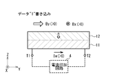
- FIG. 5 is a cross-sectional view conceptually showing a write operation of data “1” in the magnetic memory according to the first embodiment.
- FIG. 5 is a cross-sectional view conceptually showing a write operation of data “0” in the magnetic memory according to the first embodiment.
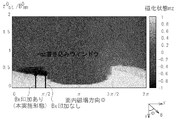
- 6 is a diagram showing a write window of a write operation of data “1” in the magnetic memory according to the first embodiment.
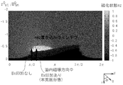
- FIG. 6 is a diagram showing a write window of a write operation of data “0” in the magnetic memory according to the first embodiment.
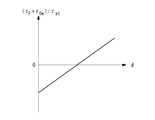
- FIG. It is a graph which shows notionally field-like torque (tau) F and torque (tau) Oe by an Oersted magnetic field. It is a top view which shows the structure of the magnetic memory of the 2nd Embodiment of this invention.
- FIG. 9B is a cross-sectional view showing a cross-sectional structure of the magnetic memory element according to the second embodiment along a cross-section AA in FIG. 8A.
- FIG. 8B is a cross-sectional view showing a cross-sectional structure of the magnetic memory element according to the second embodiment along a cross section BB in FIG. 8A.
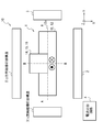
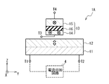
- FIG. 2A is a plan view showing the configuration of the magnetic memory 10 according to the first embodiment of the present invention.
- the direction may be indicated using xyz orthogonal coordinates.
- the magnetic memory 10 includes a magnetic memory element 1, a y-direction magnetic field application structure 2, an x-direction magnetic field application structure 3, and a current application circuit 4.
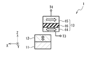
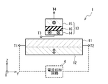
- 2B and 2C are cross-sectional views showing the structure of the magnetic memory element 1.
- FIG. 2B shows a cross-sectional structure of the magnetic memory in the cross section AA shown in FIG. 2A
- FIG. 2C shows a cross-sectional structure of the magnetic memory in the cross section BB shown in FIG. 2A. ing.
- the magnetic memory element 1 includes an adjacent layer 11, a recording layer 12, and an MTJ (magnetic tunnel junction) 13.
- the x-axis and the y-axis are defined so as to be orthogonal to each other in the in-plane direction of the adjacent layer 11 and the recording layer 12.
- the z axis is defined in the film thickness direction of the adjacent layer 11 and the recording layer 12, that is, the direction orthogonal to both the x axis and the y axis.
- the adjacent layer 11 is formed of a metal film that strongly expresses the spin Hall effect.
- the adjacent layer 11 is formed of Pt, Pd, Au, Ag, Cu, Ta, W, Nb, Mb, or an alloy containing two or more of these. It is preferable that the metal film is formed. From the viewpoint of strongly expressing the spin Hall effect, it is desirable to use a Pt film as the adjacent layer 11 among the metal films of these materials.
- a metal film doped with at least one element selected from Mn, Ir, Bi, B, C, and N (for example, Mn, Ir, It is preferably formed of a Cu film doped with at least one element selected from Bi, B, C, and N.
- first and second terminals T1 and T2 are connected.
- the first and second terminals T1 and T2 are connected to the current application circuit 4 via a selection transistor and a selector (not shown), and are connected to the adjacent layer 11 and the recording layer 12 in the y-axis direction (+ y direction or ⁇ y direction). This is used to pass the write current Iw.
- the recording layer 12 is formed of a perpendicular magnetization film having perpendicular magnetic anisotropy. That is, the magnetization of the recording layer 12 can be reversed between the + z direction and the ⁇ z direction.
- the recording layer 12 it is desirable to use a ferromagnetic or ferrimagnetic film containing at least one of Fe, Co, and Ni.
- the ferromagnetic film that can be used as the recording layer 12 include a Co / Ni laminated film (that is, a laminated film in which a plurality of Co films and a plurality of Ni films are alternately laminated), and a Co / Pd laminated film.
- a Co / Pt laminated film ie, a laminated film in which a plurality of Co films and a plurality of Pt films are alternately laminated
- a Co—Cr—Pt alloy film ie, a laminated film in which a plurality of Co films and a plurality of Pt films are alternately laminated
- ferrimagnetic film that can be used as the recording layer 12 include Gd—Fe—Co alloys, Gd—Co alloys, and Tb—Fe—Co alloy films.
- An insulating film for example, a metal oxide film (not shown) such as Mg—O or Al—O may be formed on the surface of the recording layer 12 opposite to the adjacent layer 11.
- the MTJ 13 includes a sense layer 14, a reference layer 15, and a tunnel barrier layer 16.
- the sense layer 14 is formed of a ferromagnetic material, more specifically, an in-plane magnetization film having in-plane magnetic anisotropy.
- the material of the sense layer 14 preferably includes at least one selected from Fe, Co, and Ni.
- the sense layer 14 is formed of, for example, a NiFe alloy film, a CoFeB alloy film, a CoFe alloy film, or the like.
- the sense layer 14 has a magnetization direction that can be reversed between the + x direction and the -x direction.
- the reference layer 15 is also formed of a ferromagnetic material, more specifically, an in-plane magnetization film having in-plane magnetic anisotropy.
- the reference layer 15 is formed of the same material as the sense layer 14.
- the magnetization of the reference layer 15 is fixed and is not reversed by writing and reading operations. In this embodiment, as shown in FIG. 2C, the reference layer 15 is fixed in the ⁇ x direction.
- an antiferromagnetic layer (not shown) may be stacked on the reference layer 15 in order to fix the magnetization of the reference layer 15.
- the reference layer 15 may be a laminated film in which a first ferromagnetic film, a nonmagnetic film, and a second ferromagnetic film are sequentially laminated. In this case, the magnetizations of the first and second ferromagnetic films may be set to be antiparallel to each other by antiferromagnetic coupling.
- the tunnel barrier layer 16 is an insulating nonmagnetic layer. Examples of the material of the tunnel barrier layer 16 include Mg—O, Al—O, Ni—O, and Hf—O.
- the tunnel barrier layer 16 is sandwiched between the sense layer 14 and the reference layer 15, and the MTJ 13 is formed by the sense layer 14, the tunnel barrier layer 16, and the reference layer 15.
- the sense layer 14 of the MTJ 13 is arranged such that the center of gravity in the xy plane is shifted from the center line 12a of the recording layer 12 in the ⁇ x direction. Magnetically coupled. With such an arrangement, the magnetization direction of the sense layer 14 is reversed depending on the magnetization direction of the recording layer 12.
- the sense layer 14 is connected to the third terminal T3, and the reference layer 15 is connected to the fourth terminal T4.
- a read current Ir flows through the MTJ 13 by applying a voltage between the third and fourth terminals T3 and T4.
- the resistance value of the MTJ 13 depends on the relative directions of magnetization of the sense layer 14 and the reference layer 15 due to the magnetic tunnel effect.
- the magnetization direction of the sense layer 14 is reversed depending on the magnetization direction of the recording layer 12, the magnetization direction of the recording layer 12, that is, the recording layer 12 is applied to the MTJ 13 by passing a read current Ir.
- a current signal or voltage signal representing the written data can be obtained.
- the sense layer 14 When the sense layer 14 is electrically connected to the adjacent layer 11 and the recording layer 12 (for example, a conductive layer is provided between the sense layer 14 and the recording layer 12, and the sense layer 14 is connected to the conductive layer). 3), the third terminal T3 is not provided, and the first terminal T1 and the fourth terminal T4, or the second terminal T2 and the fourth terminal.
- the read current Ir may flow during T4.
- FIGS 2A to 2C show the structure in which the sense layer 14 is closer to the recording layer 12 than the reference layer 15, the positions of the sense layer 14 and the reference layer 15 may be reversed.
- the tunnel barrier layer 16 is provided on the upper surface of the reference layer 15 and the sense layer 14 is provided on the upper surface of the tunnel barrier layer 16. There is.
- 2B and 2C show a structure in which the adjacent layer 11 is bonded to the lower surface of the recording layer 12 (that is, a structure in which the recording layer 12 is bonded to the upper surface of the adjacent layer 11).
- the positions of the adjacent layer 11 and the recording layer 12 may be reversed.
- the adjacent layer 11 is bonded to the lower surface of the recording layer 12.
- the recording layer 12 and the sense layer 14 are arranged so that they are magnetically coupled.
- the y-direction magnetic field application structure 2 and the x-direction magnetic field application structure 3 constitute an external magnetic field application unit for applying an external magnetic field in the in-plane direction of the recording layer 12.
- the y-direction magnetic field application structure 2 is configured to apply a first external magnetic field By to the recording layer 12 of the magnetic memory element 1 in a direction parallel to the y-axis direction (+ y direction or ⁇ y direction).
- a wiring is arranged in the vicinity of the magnetic memory element 1 as the y-direction magnetic field applying structure 2, and an electric current flows through the wiring, whereby an Oersted magnetic field (current magnetic field) is generated in the recording layer 12 parallel to the y-axis direction.
- a ferromagnetic material may be disposed as the y-direction magnetic field applying structure 2 and the first external magnetic field By may be applied by the ferromagnetic material in a direction parallel to the y-axis direction (+ y direction or ⁇ y direction).
- the + y direction is also called a first direction
- the -y direction is also called a second direction.
- the x-direction magnetic field application structure 3 is a structure for applying a second external magnetic field Bx to the recording layer 12 in a direction parallel to the x-axis direction (+ x direction or -x direction).
- a second external magnetic field Bx is applied to the recording layer 12 in parallel to the x-axis direction by arranging a wiring in the vicinity of the magnetic memory element 1 as the x-direction magnetic field applying structure 3 and passing a current through the wiring. Good.
- the direction of the second external magnetic field Bx applied by the x-direction magnetic field applying structure 3 is selected from the + x direction and the ⁇ x direction according to the direction of the write current Iw.
- the direction of the second external magnetic field Bx is also referred to as “first magnetic field application direction”.
- the current application circuit 4 is connected to the first and second terminals T1 and T2 of the adjacent layer 11 via a selection transistor and a selector (both not shown), and a write current is supplied to the adjacent layer 11 and the recording layer 12. Run Iw.
- the direction of the write current Iw flowing through the adjacent layer 11 and the recording layer 12 is associated with the data to be written. In one embodiment, when writing data “1”, the write current Iw is passed in the + y direction, and when writing data “0”, the write current Iw is passed in the ⁇ y direction.
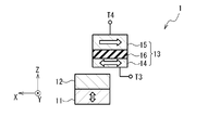
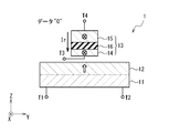
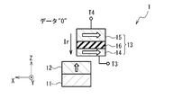
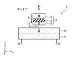
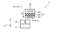
- FIGS. 4A and 4B show the two states.
- the other state (second state) is shown.
- One of the two states is associated with data “0”, and the other is associated with data “1”.
- the leakage magnetic field from the recording layer 12 is in the ⁇ x direction at the position of the sense layer 14.
- the magnetization of the sense layer 14 is directed to the ⁇ x direction according to the direction of the leakage magnetic field.
- the magnetizations of the sense layer 14 and the reference layer 15 are parallel, and the resistance value of the MTJ 13 is low (low resistance state). This low resistance state is associated with, for example, data “0”.
- the leakage magnetic field from the recording layer 12 has a component in the + x direction at the position of the sense layer 14. Then, the magnetization of the sense layer 14 is directed in the + x direction according to the direction of the leakage magnetic field.
- the magnetizations of the sense layer 14 and the reference layer 15 are antiparallel, and the resistance value of the MTJ 13 is high (high resistance state). This high resistance state is associated with, for example, data “1”.
- Data reading is performed by passing a read current Ir between the third and fourth terminals T3 and T4.
- the read current Ir flows through the MTJ 13 so as to penetrate the tunnel barrier layer 16.
- the resistance value of the MTJ 13 represents the relative direction of magnetization of the sense layer 14 and the reference layer 15, that is, the data stored in the recording layer 12, and is thus generated from the read current Ir or the read current Ir.
- the data stored in the recording layer 12 can be identified based on the read voltage.
- (Write operation) 5A and 5B are conceptual diagrams illustrating an example of a write operation of the memory element according to the present embodiment.
- the MTJ 13 not related to the write operation is not shown in FIGS. 5A and 5B.
- a thin film for example, a Pt film made of a material in which the adjacent layer 11 is bonded to the lower surface of the recording layer 12 and the spin hole angle is positive as the adjacent layer 11.
- the first external magnetic field By is applied to the recording layer 12 in the + y direction by the y-direction magnetic field applying structure 2.
- FIG. 5A shows the magnetization state of data “1” after writing.
- the write current Iw is applied to the adjacent layer 11 by the current application circuit 4 as shown in FIG. 5B.
- a current flows through the recording layer 12 in the ⁇ y direction (that is, from the second terminal T2 to the first terminal T1).
- Slonczewski-like torque tau st -x direction of the torque is generated.
- the magnitude of the write current Iw exceeds the inversion threshold current, the magnetization of the recording layer 12 is reversed from the ⁇ z direction to the + z direction.
- FIG. 5B shows the magnetization state of data “0” after writing.
- the write window can be enlarged by applying the second external magnetic field Bx in the x-axis direction.
- the write window means the range of the magnitude and direction of the write current and the external magnetic field applied in the in-plane direction so that the magnetic memory element 1 is not in the intermediate state.
- the direction of the second external magnetic field Bx (the first magnetic field application direction) is selected in the same direction as the Slonczewski-like torque ⁇ st that acts on the magnetization of the recording layer 12.
- the write current Iw is + y between the adjacent layer 11 and the recording layer 12.
- a torque in the + x direction is generated as the Slonczewski-like torque ⁇ st .
- the second external magnetic field Bx is applied in the + x direction by the x-direction magnetic field application structure 3.
- the second external magnetic field Bx is a positive value.
- the write current Iw flows in the ⁇ y direction between the adjacent layer 11 and the recording layer 12.
- a torque in the ⁇ x direction is generated as the Slonczewski-like torque ⁇ st .
- Bx is applied in the ⁇ x direction by the x-direction magnetic field applying structure 3.
- the second external magnetic field Bx is a negative value.
- the direction of the write current Iw is opposite to the direction illustrated in FIGS. 5A and 5B. Is done. That is, when data “1” is written to the magnetic memory element 1, the write current Iw is caused to flow in the ⁇ y direction, and when data “0” is written to the magnetic memory element 1, the write current Iw is directed to the + y direction. Washed away.
- the positions of the adjacent layer 11 and the recording layer 12 are opposite to the positions of the adjacent layer 11 and the recording layer 12 shown in FIGS. 5A and 5B (that is, the adjacent layer 11 is bonded to the upper surface of the recording layer 12).
- the direction in which the write current Iw flows is also reversed from the direction shown in FIGS. 5A and 5B.
- the direction of the second external magnetic field Bx applied in the x-axis direction is Slonczewski-like. It is reversed according to the direction of the torque ⁇ st .
- the write current Iw is ⁇ y when the data “1” is written to the magnetic memory element 1.
- a second external magnetic field Bx is applied in the + x direction (Bx> 0).
- the write current Iw is supplied in the + y direction and the second external magnetic field
- the positions of the adjacent layer 11 and the recording layer 12 are opposite to the positions of the adjacent layer 11 and the recording layer 12 shown in FIGS. 5A and 5B (that is, the adjacent layer 11 is bonded to the upper surface of the recording layer 12).
- the direction of the write current Iw is reversed from the direction shown in FIGS. 5A and 5B, and the direction of the second external magnetic field Bx applied in the x-axis direction (first magnetic field application direction) is The directions are the same as those shown in FIGS. 5A and 5B.
- the inventors of the present invention confirmed the effect of expanding the writing window by applying the second external magnetic field Bx in the x-axis direction by simulation.
- FIGS. 6A and 6B are diagrams illustrating an example of a write window of the magnetic memory element 1 according to the present embodiment, obtained by simulation.
- the simulations of FIGS. 6A and 6B were performed with an external magnetic field
- FIG. 6A shows the dependence of the component in the z-axis direction of the magnetization of the recording layer 12 after writing from data “0” to data “1” on the in-plane magnetic field azimuth ⁇ and the Slonczewski-like torque, that is, normal Shows a write window in which data “1” can be written.
- the shading at each position in FIG. 6A represents a value obtained by normalizing the component mz in the z direction of the magnetization of the recording layer 12 after writing to a value between ⁇ 1 and 1 inclusive, and the component mz is “ ⁇ 1”.
- an area close to “ ⁇ 1” represents a write window in the write operation of data “1”.
- the writing window of data “1” is distributed in the range of the in-plane magnetic field azimuth angle ⁇ from 0 to ⁇ / 2. It should be noted that when the in-plane magnetic field azimuth angle ⁇ is in the range of 0 to ⁇ / 2, the second external magnetic field Bx (Bx> 0) is applied in the + x direction. When a Slonczewski-like torque larger than the upper end of the write window for data “1” is applied (that is, when an excessive write current Iw is supplied), an intermediate state occurs and there is a risk of erroneous writing.
- the second external magnetic field Bx can be applied in the x-axis direction (in the + x direction in the example of FIG. 6A).
- the internal magnetic field azimuth angle ⁇ can be adjusted to a desired value between 0 and ⁇ / 2. Therefore, it is expected that data can be stably written even if misalignment of the first external magnetic field By or variation in magnetic anisotropy of the recording layer 12 occurs.
- FIG. 6B shows the dependence of the component in the z-axis direction of the magnetization of the recording layer 12 after writing from data “1” to data “0” on the in-plane magnetic field azimuth ⁇ and the Slonczewski-like torque, that is, normal Shows a write window in which data “0” can be written.
- the shading at each position in FIG. 6B represents a value obtained by normalizing the component mz in the z direction of the magnetization of the recording layer 12 after writing to a value of ⁇ 1 or more and 1 or less.
- An area where mz is “+1” or a value close to “+1” represents a write window in the write operation of data “0”.
- the writing window of data “0” has an in-plane magnetic field azimuth angle ⁇ distributed in the range of ⁇ / 2 to ⁇ .
- the in-plane magnetic field azimuth angle ⁇ is in the range of ⁇ / 2 to ⁇
- (Bx ⁇ 0) is applied in the ⁇ x direction.
- a Slonczewski-like torque larger than the upper end of the write window for data “0” is applied (that is, when an excessive write current Iw is supplied), an intermediate state occurs and there is a risk of erroneous writing.
- the second external magnetic field Bx can be applied in the x-axis direction ( ⁇ x direction in the example of FIG. 6B)
- the internal magnetic field azimuth angle ⁇ can be adjusted to a desired value from ⁇ / 2 to ⁇ . Therefore, it is expected that data can be stably written even if misalignment of the first external magnetic field By or variation in magnetic anisotropy of the recording layer occurs.
- the writing window of data “0” is distributed in the range of the in-plane magnetic field azimuth angle ⁇ from ⁇ to 3 ⁇ / 2
- the writing window of data “1” is from the in-plane magnetic field azimuth angle ⁇ of 3 ⁇ / 2. It is distributed in the range of 2 ⁇ .
- the direction of the second external magnetic field Bx (first magnetic field application direction) is such that the in-plane magnetic field azimuth angle ⁇ is in the range of ⁇ to 3 ⁇ / 2 when data “0” is written, and the surface when data “1” is written.
- the internal magnetic field azimuth angle ⁇ is set in the range of ⁇ to 3 ⁇ / 2.
- the data “0” and “1” are merely associated with one of the two states of the magnetic memory element 1 and the other state.
- the definitions of data “0” and “1” are interchanged (that is, the state in which the magnetization of the recording layer 12 is oriented in the ⁇ z direction is defined as data “0”, and the magnetization of the recording layer 12 is in the + z direction)
- the definition of the write window for data “0” and the definition of the write window for data “1” are interchanged.
- the magnetic memory according to the present embodiment can stably write data when writing data using in-plane current induced vertical magnetization reversal.
- the total torque ⁇ tot acting on the magnetization is the Slonczewski-like torque ⁇ st including the contribution from the Rashba field induced by the current and the spin Hall effect, and the torque ⁇ ext due to the external magnetic field.
- the torque ⁇ an due to magnetic anisotropy.
- the write current Iw flowing through the adjacent layer 11 generates an Oersted magnetic field (current magnetic field), and the write current Iw flowing through the adjacent layer 11 and the recording layer 12 is And the field-like torque including the contribution from the spin Hall effect is generated, and in order to represent the motion of magnetization more accurately, the Oersted magnetic field and the field-like torque should be considered.
- Equation (2) representing the total torque ⁇ tot is changed to the following equation (7):
- ⁇ F is a field-like torque generated when the write current Iw flows through the adjacent layer 11 and the recording layer 12
- ⁇ Oe is a torque due to the Oersted magnetic field when the write current Iw flows through the adjacent layer 11.
- B 0 F is a magnitude including the sign of the field-like torque
- B 0 Oe is a magnitude including the sign of the Oersted magnetic field. Note that both the field-like torque and the Oersted field direction depend on the direction of the write current.
- B 0 F and B 0 Oe are second external magnetic fields Bx applied from the outside in the x-axis direction (that is, applied by the x-direction magnetic field applying structure 3). It is understood that it is equivalent to 2 external magnetic fields Bx).
- B 0 F is referred to as an effective magnetic field by field-like torque.
- the magnitude and direction of the second external magnetic field Bx applied by the x-direction magnetic field applying structure 3 are set to a desired direction corresponding to the direction of the write current Iw in which the effective magnetic field Bx ′ is in the + x direction or the ⁇ x direction.
- the direction of the second external magnetic field Bx applied by the x-direction magnetic field applying structure 3 does not necessarily coincide with the direction of the effective magnetic field Bx ′.
- the direction of the effective magnetic field Bx ′ is also referred to as “third magnetic field application direction”.
- the adjacent layer 11 is bonded to the lower surface of the recording layer 12, a thin film (for example, a Pt film) made of a material having a positive spin hole angle is used as the adjacent layer 11, and the recording layer 12 is used.
- a thin film for example, a Pt film
- the write operation is performed as follows.
- the sum of the effective magnetic field B 0 F and the Oersted magnetic field B 0 Oe by the field-like torque is the material and film thickness of the adjacent layer 11 and the recording layer 12. Note that it is adjustable by. If the sum of the effective magnetic field B 0 F and the Oersted magnetic field B 0 Oe by the field-like torque is controlled by the material and film thickness of the adjacent layer 11 and the recording layer 12, the second external magnetic field Bx is applied to the x-direction magnetic field. This means that the desired effective magnetic field Bx ′ can be realized without application by the structure 3.
- FIG. 7 shows the dependence of the sum of the field-like torque ⁇ F and the torque ⁇ Oe due to the Oersted magnetic field on the Co film in the structure in which the Co film and the Pt film are laminated as disclosed in Non-Patent Document 5. It is a figure which shows an example of no.
- Non-Patent Document 5 discloses that the sum of the field-like torque ⁇ F and the torque ⁇ Oe due to the Oersted magnetic field increases as the thickness d Co of the Co film increases. As understood from the above formulas (8) and (9), this is because the sum of the effective magnetic field B 0 F and the Oersted magnetic field B 0 Oe due to the field-like torque increases the thickness d Co of the Co film. It is equivalent to increasing with the increase.
- the direction of the sum of the effective magnetic field B 0 F and the Oersted magnetic field B 0 Oe is also referred to as “second magnetic field application direction”.
- FIGS. 8A to 8C are plan views showing examples of the structure of the magnetic memory 10A that realizes a desired effective magnetic field Bx ′ without using the x-direction magnetic field application structure 3 that applies the second external magnetic field Bx in the x-axis direction. is there.
- the x-direction magnetic field application structure 3 is not provided. Instead, the sum of the effective magnetic field B 0 F and the Oersted magnetic field B 0 Oe by the field-like torque is adjusted according to the material and film thickness of the adjacent layer 11 and the recording layer 12 of the magnetic memory element 1A. A desired effective magnetic field Bx ′ is realized. Even with such a configuration, the writing window can be widened and data can be stably written.
- the structure shown in FIGS. 8A to 8C without the x-direction magnetic field applying structure 3 is effective for reducing the area of the magnetic memory 10A.
- Magnetic memory 1A Magnetic memory element 2: y-direction magnetic field application structure 3: x-direction magnetic field application structure 4: current application circuit 11: adjacent layer 12: recording layer 12a: center line 13: MTJ 14: Sense layer 15: Reference layer 16: Tunnel barrier layer 101: Adjacent layer 102: Perpendicular magnetization film
Landscapes
- Engineering & Computer Science (AREA)
- Computer Hardware Design (AREA)
- Mram Or Spin Memory Techniques (AREA)
- Hall/Mr Elements (AREA)
Abstract
Description


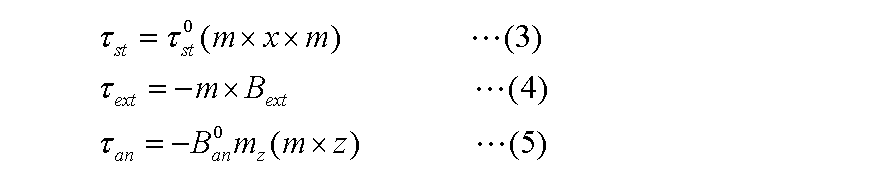
図2Aは、本発明の第1の実施形態の磁気メモリ10の構成を示す平面図である。なお、以下の磁気メモリ10についての説明においては、xyz直交座標を用いて方向を示すことがある。
図3A、図3Bは、本実施形態において磁気メモリ素子1がとりうる2つの状態のうちの一方の状態(第1の状態)を示し、図4A、図4Bは、該2つの状態のうちの他方の状態(第2の状態)を示している。該2つの状態の一方がデータ“0”に対応づけられ、他方がデータ“1”に対応付けられる。
図5A及び図5Bは、本実施形態に係る記憶素子の書き込み動作の一例を示す概念図である。なお、以下では書き込み動作を説明するため、図5A、図5Bにおいては、書き込み動作に関係しないMTJ13は図示していない。
(a)隣接層11の材料のスピンホール角の符号
(b)y軸方向に印加する第1外部磁場Byの方向(+y方向又は-y方向)
(c)隣接層11と記録層12の位置関係
本発明者らは、x軸方向への第2外部磁場Bxの印加による書き込みウィンドウの拡大の効果をシミュレーションにより確認した。
tanΦ=By/Bx, ・・・(6a)
即ち、下記式(6b)
Φ=arctan(By/Bx) ・・・(6b)
で定義される。なお、第2および第1外部磁場Bx、Byは、それぞれ、図2A~図2Cに図示された+x方向、+y方向の向きが正であると定義されている。図6A及び図6Bの縦軸は異方性磁場の大きさで規格化されたSlonczewski-likeトルクであり、書き込み電流Iwの大きさに対応している。
上記の式(2)によれば、磁化に作用する全トルクτtotは、電流によって誘起されるラシュバ場とスピンホール効果からの寄与を含むSlonczewski-likeトルクτstと、外部磁場によるトルクτextと、磁気異方性によるトルクτanとの和として表される。


Bx’=Bx+B0 F+B0 Oe ・・・(10)
で定義したとき、第2外部磁場Bxの代わりに実効磁場Bx’を用いれば、第1の実施形態に提示した議論よりも一層に正確な議論が成立する。即ち、x方向磁場印加構造3によって印加される第2外部磁場Bxの大きさと方向を、実効磁場Bx’の方向が+x方向又は-x方向のうちの書き込み電流Iwの向きに応じた所望の方向になるように決定することで、データ書き込みにおける書き込みウィンドウを拡大することができる。ここで、x方向磁場印加構造3によって印加される第2外部磁場Bxの方向は、必ずしも、実効磁場Bx’の方向に一致しないことに留意されたい。なお、実効磁場Bx’の方向は、「第3磁場印加方向」とも呼ばれる。
tanΦ’=By/Bx’ ・・・(11a)
即ち、下記式(11b)
Φ’=arctan(By/Bx’) ・・・(11b)
で定義された実効面内磁場方位角Φ’を面内磁場方位角Φの代わりに適用することにより、第1の実施形態と同様の議論が妥当する。
1、1A :磁気メモリ素子
2 :y方向磁場印加構造
3 :x方向磁場印加構造
4 :電流印加回路
11 :隣接層
12 :記録層
12a :中心線
13 :MTJ
14 :センス層
15 :リファレンス層
16 :トンネルバリア層
101 :隣接層
102 :垂直磁化膜
Claims (11)
- 垂直磁化膜として形成された記録層と、
前記記録層の上面又は下面に接合される隣接層と、
前記記録層の面内方向である第1方向に前記記録層に第1外部磁場を印加するように構成された外部磁場印加部と、
前記隣接層と前記記録層とに、前記第1方向又は前記第1方向と逆の第2方向に書き込み電流を流すように構成された電流印加部と
を具備し、
前記記録層と前記隣接層と前記外部磁場印加部とは、第1乃至第3磁場印加方向のいずれかを、前記書き込み電流の方向に応じて反転するように構成されており、前記第1磁場印加方向は前記第1方向に垂直な方向に印加される第2外部磁場の方向であり、前記第2磁場印加方向は前記書き込み電流が前記隣接層と前記記録層とに流れることによって生じるfield-likeトルクによる有効磁場と前記書き込み電流が前記隣接層に流れることによって生成されるエルステッド磁場との和の方向であり、前記第3磁場印加方向は前記第2外部磁場と前記有効磁場と前記エルステッド磁場との和である実効磁場の方向である
磁気メモリ。 - 請求項1に記載の磁気メモリであって、
前記外部磁場印加部は、
前記第1外部磁場を生成する第1外部磁場印加構造と、
前記第2外部磁場を生成する第2外部磁場印加構造と
を備え、
前記第1磁場印加方向が、前記書き込み電流の方向に応じて反転される
磁気メモリ。 - 請求項2に記載の磁気メモリであって、
前記第2外部磁場は、前記書き込み電流が前記隣接層と前記記録層とに流れることによって生じるSlonczewski-likeトルクと同一の方向に印加される
磁気メモリ。 - 請求項2に記載の磁気メモリであって、
面内磁場角度Φを、arctan(By/Bx)で定義したとき(Byは、前記第1方向に向く場合を正としたときの前記第1外部磁場であり、Bxは、前記第2外部磁場である)、
前記第1外部磁場Byが正のとき、前記第2外部磁場印加構造は、データ“0”又はデータ“1”のうち一方のデータを前記記録層に書き込む場合には前記面内磁場角度Φが0より大きくπ/2未満であり、他方のデータを書き込む場合には前記面内磁場角度Φがπ/2より大きくπ未満であるように前記第2外部磁場を印加し、
前記第1外部磁場Byが負のとき、前記第2外部磁場印加構造は、データ“0”又はデータ“1”のうち一方のデータを前記記録層に書き込む場合には前記面内磁場角度Φがπより大きく、3π/2未満であるように前記第2外部磁場を印加し、他方のデータを書き込む場合には3π/2より大きく、2π未満であるように前記第2外部磁場を印加する
磁気メモリ。 - 請求項1に記載の磁気メモリであって、
前記外部磁場印加部は、
前記第1外部磁場を生成する第1外部磁場印加構造と、
前記第2外部磁場を生成する第2外部磁場印加構造と
を備え、
前記第2外部磁場印加構造は、前記第3磁場印加方向が前記書き込み電流の方向に応じて反転されるように前記第2外部磁場を生成する
磁気メモリ。 - 請求項5に記載の磁気メモリであって、
実効面内磁場角度Φ’を、arctan(By/Bx’)で定義したとき(Byは、前記第1方向に向く場合を正としたときの前記第1外部磁場であり、Bx’は、前記実効磁場である)、
前記第1外部磁場Byが正のとき、前記第2外部磁場印加構造は、データ“0”又はデータ“1”のうち一方のデータを前記記録層に書き込む場合には前記実効面内磁場角度Φ’が0より大きくπ/2未満であり、他方のデータを書き込む場合には前記実効面内磁場角度Φ’がπ/2より大きくπ未満であるように前記第2外部磁場を印加し、
前記第1外部磁場Byが負のとき、前記第2外部磁場印加構造は、データ“0”又はデータ“1”のうち一方のデータを前記記録層に書き込む場合には前記実効面内磁場角度Φ’がπより大きく、3π/2未満であるように前記第2外部磁場を印加し、他方のデータを書き込む場合には前記実効面内磁場角度Φ’が3π/2より大きく、2π未満であるように前記第2外部磁場を印加する
磁気メモリ。 - 請求項1に記載の磁気メモリであって、
前記記録層と前記隣接層と前記外部磁場印加部とは、前記第2磁場印加方向を、前記書き込み電流の方向に応じて反転するように構成され、
前記記録層には、前記第1方向に垂直な方向の外部磁場は印加されない
磁気メモリ。 - 請求項1乃至7のいずれかに記載の磁気メモリであって、
前記記録層は、Fe、Co、Niのうちの少なくとも一以上を含むフェロ磁性体又はフェリ磁性体の膜を含む
磁気メモリ。 - 請求項1乃至8のいずれかに記載の磁気メモリであって、
前記隣接層は、Pt、Pd、Au、Ag、Cu、Ta、W、Nb、Mb、又は、これらのうちの2以上を含む合金で形成された金属膜を含む
磁気メモリ。 - 垂直磁化膜として形成された記録層と前記記録層の上面又は下面に接合される隣接層とを含む磁気メモリ素子へのデータ書き込み方法であって、
前記記録層の面内方向である第1方向に前記記録層に第1外部磁場を印加することと、
前記隣接層と前記記録層とに、前記第1方向又は前記第1方向と逆の第2方向に書き込み電流を流すことと、
前記第1方向に垂直な方向に第2外部磁場を印加することと
を具備し、
前記第2外部磁場の方向、又は、前記書き込み電流が前記隣接層と前記記録層とに流れることによって生じるfield-likeトルクによる有効磁場と前記書き込み電流が前記隣接層に流れることによって生成されるエルステッド磁場と前記第2外部磁場との和である実効磁場の方向が、前記書き込み電流の方向に応じて反転される
磁気メモリ素子へのデータ書き込み方法。 - 垂直磁化膜として形成された記録層と前記記録層の上面又は下面に接合される隣接層とを含む磁気メモリ素子へのデータ書き込み方法であって、
前記記録層の面内方向である第1方向に前記記録層に第1外部磁場を印加することと、
前記隣接層と前記記録層とに、前記第1方向又は前記第1方向と逆の第2方向に書き込み電流を流すことと
を具備し、
前記書き込み電流が前記隣接層と前記記録層とに流れることによって生じるfield-likeトルクによる有効磁場と前記書き込み電流によって生成されるエルステッド磁場との和の方向が、前記書き込み電流の方向に応じて反転される 磁気メモリ素子へのデータ書き込み方法。
Priority Applications (2)
| Application Number | Priority Date | Filing Date | Title |
|---|---|---|---|
| US15/519,851 US10037789B2 (en) | 2014-10-21 | 2015-08-31 | Magnetic memory and method for writing data into magnetic memory element |
| JP2016555054A JP6674167B2 (ja) | 2014-10-21 | 2015-08-31 | 磁気メモリ及び磁気メモリ素子へのデータ書き込み方法 |
Applications Claiming Priority (2)
| Application Number | Priority Date | Filing Date | Title |
|---|---|---|---|
| JP2014214729 | 2014-10-21 | ||
| JP2014-214729 | 2014-10-21 |
Publications (1)
| Publication Number | Publication Date |
|---|---|
| WO2016063448A1 true WO2016063448A1 (ja) | 2016-04-28 |
Family
ID=55760511
Family Applications (1)
| Application Number | Title | Priority Date | Filing Date |
|---|---|---|---|
| PCT/JP2015/004399 Ceased WO2016063448A1 (ja) | 2014-10-21 | 2015-08-31 | 磁気メモリ及び磁気メモリ素子へのデータ書き込み方法 |
Country Status (3)
| Country | Link |
|---|---|
| US (1) | US10037789B2 (ja) |
| JP (1) | JP6674167B2 (ja) |
| WO (1) | WO2016063448A1 (ja) |
Cited By (3)
| Publication number | Priority date | Publication date | Assignee | Title |
|---|---|---|---|---|
| CN108987562A (zh) * | 2017-06-02 | 2018-12-11 | 桑迪士克科技有限责任公司 | 磁阻式随机存取存储器的复合自由层 |
| JP2019009478A (ja) * | 2017-02-27 | 2019-01-17 | Tdk株式会社 | スピン流磁化回転素子、磁気抵抗効果素子及び磁気メモリ |
| CN111183480A (zh) * | 2017-11-21 | 2020-05-19 | 闪迪技术有限公司 | 用于磁阻随机存取存储器的复合自由层 |
Families Citing this family (4)
| Publication number | Priority date | Publication date | Assignee | Title |
|---|---|---|---|---|
| US10475988B2 (en) * | 2016-07-27 | 2019-11-12 | National University Of Singapore | High efficiency spin torque switching using a ferrimagnet |
| US11093824B2 (en) * | 2016-09-02 | 2021-08-17 | Samsung Electronics Co., Ltd. | Neuromorphic device and method of driving the same |
| US10276784B1 (en) * | 2017-10-30 | 2019-04-30 | Taiwan Semiconductor Manufacturing Company Ltd. | Semiconductor structure and associated operating and fabricating method |
| US10891999B1 (en) * | 2019-06-19 | 2021-01-12 | Western Digital Technologies, Inc. | Perpendicular SOT MRAM |
Citations (3)
| Publication number | Priority date | Publication date | Assignee | Title |
|---|---|---|---|---|
| JP2010003850A (ja) * | 2008-06-19 | 2010-01-07 | Tohoku Univ | 磁気素子及び集積回路並びに磁気ランダムアクセスメモリ |
| WO2014011533A1 (en) * | 2012-07-10 | 2014-01-16 | New York University | Precessional reversal in orthogonal spin transfer magnetic ram devices |
| JP2014143302A (ja) * | 2013-01-24 | 2014-08-07 | Nec Corp | 磁気メモリセル及び磁気ランダムアクセスメモリ |
Family Cites Families (3)
| Publication number | Priority date | Publication date | Assignee | Title |
|---|---|---|---|---|
| JP4157707B2 (ja) | 2002-01-16 | 2008-10-01 | 株式会社東芝 | 磁気メモリ |
| JP2006310423A (ja) | 2005-04-27 | 2006-11-09 | Nec Corp | 磁気メモリ及びその製造方法 |
| JP5152712B2 (ja) | 2007-07-17 | 2013-02-27 | 独立行政法人理化学研究所 | 磁化状態制御装置および磁気情報記録装置 |
-
2015
- 2015-08-31 WO PCT/JP2015/004399 patent/WO2016063448A1/ja not_active Ceased
- 2015-08-31 US US15/519,851 patent/US10037789B2/en active Active
- 2015-08-31 JP JP2016555054A patent/JP6674167B2/ja active Active
Patent Citations (3)
| Publication number | Priority date | Publication date | Assignee | Title |
|---|---|---|---|---|
| JP2010003850A (ja) * | 2008-06-19 | 2010-01-07 | Tohoku Univ | 磁気素子及び集積回路並びに磁気ランダムアクセスメモリ |
| WO2014011533A1 (en) * | 2012-07-10 | 2014-01-16 | New York University | Precessional reversal in orthogonal spin transfer magnetic ram devices |
| JP2014143302A (ja) * | 2013-01-24 | 2014-08-07 | Nec Corp | 磁気メモリセル及び磁気ランダムアクセスメモリ |
Cited By (5)
| Publication number | Priority date | Publication date | Assignee | Title |
|---|---|---|---|---|
| JP2019009478A (ja) * | 2017-02-27 | 2019-01-17 | Tdk株式会社 | スピン流磁化回転素子、磁気抵抗効果素子及び磁気メモリ |
| CN108987562A (zh) * | 2017-06-02 | 2018-12-11 | 桑迪士克科技有限责任公司 | 磁阻式随机存取存储器的复合自由层 |
| CN108987562B (zh) * | 2017-06-02 | 2022-09-27 | 桑迪士克科技有限责任公司 | 磁阻式随机存取存储器的复合自由层 |
| CN111183480A (zh) * | 2017-11-21 | 2020-05-19 | 闪迪技术有限公司 | 用于磁阻随机存取存储器的复合自由层 |
| CN111183480B (zh) * | 2017-11-21 | 2023-10-03 | 闪迪技术有限公司 | 用于磁阻随机存取存储器的复合自由层 |
Also Published As
| Publication number | Publication date |
|---|---|
| JP6674167B2 (ja) | 2020-04-01 |
| JPWO2016063448A1 (ja) | 2017-08-03 |
| US20170249981A1 (en) | 2017-08-31 |
| US10037789B2 (en) | 2018-07-31 |
Similar Documents
| Publication | Publication Date | Title |
|---|---|---|
| JP6290487B1 (ja) | 磁気メモリ | |
| JP5514059B2 (ja) | 磁気抵抗効果素子及び磁気ランダムアクセスメモリ | |
| CN101689600B (zh) | 磁阻效应元件及磁性随机存取存储器 | |
| KR101266791B1 (ko) | 면내 전류와 전기장을 이용한 자기메모리 소자 | |
| JP6674167B2 (ja) | 磁気メモリ及び磁気メモリ素子へのデータ書き込み方法 | |
| JP5260040B2 (ja) | 単一方向電流磁化反転磁気抵抗効果素子と磁気記録装置 | |
| JP6029020B2 (ja) | 磁気メモリ素子および磁気メモリ | |
| US11056641B2 (en) | Spin-orbit-torque magnetization rotational element, spin-orbit-torque magnetoresistance effect element, and magnetic memory | |
| US10971293B2 (en) | Spin-orbit-torque magnetization rotational element, spin-orbit-torque magnetoresistance effect element, and spin-orbit-torque magnetization rotational element manufacturing method | |
| JP2006303159A (ja) | スピン注入磁区移動素子およびこれを用いた装置 | |
| JPWO2019031226A1 (ja) | スピン流磁気抵抗効果素子及び磁気メモリ | |
| CN102403026A (zh) | 存储元件和存储装置 | |
| JP6434103B1 (ja) | 磁気メモリ | |
| JP2006287081A (ja) | スピン注入磁区移動素子およびこれを用いた装置 | |
| JPWO2016182085A1 (ja) | 磁気抵抗効果素子及び磁気メモリ装置 | |
| JP5445970B2 (ja) | 磁気抵抗効果素子及び磁気ランダムアクセスメモリ | |
| JP2014072394A (ja) | 記憶素子、記憶装置、磁気ヘッド | |
| JP2018195730A (ja) | スピン流磁化反転素子 | |
| JP5278769B2 (ja) | 磁気記録装置及び磁化固定方法 | |
| TW201222546A (en) | Memory element and memory device | |
| JP2018014376A (ja) | 双極性電圧書き込み型磁気メモリ素子 | |
| JP4492052B2 (ja) | 磁気記憶セルおよび磁気メモリデバイス | |
| JP2010219156A (ja) | 磁壁移動素子、及び、磁気ランダムアクセスメモリ | |
| US9424903B2 (en) | Memory apparatus and memory device | |
| JP5327543B2 (ja) | 磁気ランダムアクセスメモリ |
Legal Events
| Date | Code | Title | Description |
|---|---|---|---|
| 121 | Ep: the epo has been informed by wipo that ep was designated in this application |
Ref document number: 15851721 Country of ref document: EP Kind code of ref document: A1 |
|
| ENP | Entry into the national phase |
Ref document number: 2016555054 Country of ref document: JP Kind code of ref document: A |
|
| WWE | Wipo information: entry into national phase |
Ref document number: 15519851 Country of ref document: US |
|
| NENP | Non-entry into the national phase |
Ref country code: DE |
|
| 122 | Ep: pct application non-entry in european phase |
Ref document number: 15851721 Country of ref document: EP Kind code of ref document: A1 |