WO2016059732A1 - 粉粒体の塗布方法 - Google Patents
粉粒体の塗布方法 Download PDFInfo
- Publication number
- WO2016059732A1 WO2016059732A1 PCT/JP2014/081877 JP2014081877W WO2016059732A1 WO 2016059732 A1 WO2016059732 A1 WO 2016059732A1 JP 2014081877 W JP2014081877 W JP 2014081877W WO 2016059732 A1 WO2016059732 A1 WO 2016059732A1
- Authority
- WO
- WIPO (PCT)
- Prior art keywords
- substrate
- powder
- coated
- applying
- led
- Prior art date
Links
Images


Classifications
-
- H—ELECTRICITY
- H05—ELECTRIC TECHNIQUES NOT OTHERWISE PROVIDED FOR
- H05B—ELECTRIC HEATING; ELECTRIC LIGHT SOURCES NOT OTHERWISE PROVIDED FOR; CIRCUIT ARRANGEMENTS FOR ELECTRIC LIGHT SOURCES, IN GENERAL
- H05B33/00—Electroluminescent light sources
- H05B33/10—Apparatus or processes specially adapted to the manufacture of electroluminescent light sources
-
- H—ELECTRICITY
- H01—ELECTRIC ELEMENTS
- H01L—SEMICONDUCTOR DEVICES NOT COVERED BY CLASS H10
- H01L33/00—Semiconductor devices with at least one potential-jump barrier or surface barrier specially adapted for light emission; Processes or apparatus specially adapted for the manufacture or treatment thereof or of parts thereof; Details thereof
- H01L33/44—Semiconductor devices with at least one potential-jump barrier or surface barrier specially adapted for light emission; Processes or apparatus specially adapted for the manufacture or treatment thereof or of parts thereof; Details thereof characterised by the coatings, e.g. passivation layer or anti-reflective coating
-
- B—PERFORMING OPERATIONS; TRANSPORTING
- B05—SPRAYING OR ATOMISING IN GENERAL; APPLYING FLUENT MATERIALS TO SURFACES, IN GENERAL
- B05D—PROCESSES FOR APPLYING FLUENT MATERIALS TO SURFACES, IN GENERAL
- B05D1/00—Processes for applying liquids or other fluent materials
- B05D1/02—Processes for applying liquids or other fluent materials performed by spraying
- B05D1/12—Applying particulate materials
-
- B—PERFORMING OPERATIONS; TRANSPORTING
- B05—SPRAYING OR ATOMISING IN GENERAL; APPLYING FLUENT MATERIALS TO SURFACES, IN GENERAL
- B05D—PROCESSES FOR APPLYING FLUENT MATERIALS TO SURFACES, IN GENERAL
- B05D3/00—Pretreatment of surfaces to which liquids or other fluent materials are to be applied; After-treatment of applied coatings, e.g. intermediate treating of an applied coating preparatory to subsequent applications of liquids or other fluent materials
- B05D3/06—Pretreatment of surfaces to which liquids or other fluent materials are to be applied; After-treatment of applied coatings, e.g. intermediate treating of an applied coating preparatory to subsequent applications of liquids or other fluent materials by exposure to radiation
-
- C—CHEMISTRY; METALLURGY
- C23—COATING METALLIC MATERIAL; COATING MATERIAL WITH METALLIC MATERIAL; CHEMICAL SURFACE TREATMENT; DIFFUSION TREATMENT OF METALLIC MATERIAL; COATING BY VACUUM EVAPORATION, BY SPUTTERING, BY ION IMPLANTATION OR BY CHEMICAL VAPOUR DEPOSITION, IN GENERAL; INHIBITING CORROSION OF METALLIC MATERIAL OR INCRUSTATION IN GENERAL
- C23C—COATING METALLIC MATERIAL; COATING MATERIAL WITH METALLIC MATERIAL; SURFACE TREATMENT OF METALLIC MATERIAL BY DIFFUSION INTO THE SURFACE, BY CHEMICAL CONVERSION OR SUBSTITUTION; COATING BY VACUUM EVAPORATION, BY SPUTTERING, BY ION IMPLANTATION OR BY CHEMICAL VAPOUR DEPOSITION, IN GENERAL
- C23C24/00—Coating starting from inorganic powder
- C23C24/02—Coating starting from inorganic powder by application of pressure only
- C23C24/04—Impact or kinetic deposition of particles
-
- H—ELECTRICITY
- H01—ELECTRIC ELEMENTS
- H01L—SEMICONDUCTOR DEVICES NOT COVERED BY CLASS H10
- H01L33/00—Semiconductor devices with at least one potential-jump barrier or surface barrier specially adapted for light emission; Processes or apparatus specially adapted for the manufacture or treatment thereof or of parts thereof; Details thereof
- H01L33/48—Semiconductor devices with at least one potential-jump barrier or surface barrier specially adapted for light emission; Processes or apparatus specially adapted for the manufacture or treatment thereof or of parts thereof; Details thereof characterised by the semiconductor body packages
- H01L33/50—Wavelength conversion elements
- H01L33/505—Wavelength conversion elements characterised by the shape, e.g. plate or foil
-
- H—ELECTRICITY
- H01—ELECTRIC ELEMENTS
- H01L—SEMICONDUCTOR DEVICES NOT COVERED BY CLASS H10
- H01L2933/00—Details relating to devices covered by the group H01L33/00 but not provided for in its subgroups
- H01L2933/0008—Processes
- H01L2933/0025—Processes relating to coatings
-
- H—ELECTRICITY
- H01—ELECTRIC ELEMENTS
- H01L—SEMICONDUCTOR DEVICES NOT COVERED BY CLASS H10
- H01L2933/00—Details relating to devices covered by the group H01L33/00 but not provided for in its subgroups
- H01L2933/0008—Processes
- H01L2933/0033—Processes relating to semiconductor body packages
- H01L2933/0041—Processes relating to semiconductor body packages relating to wavelength conversion elements
-
- Y—GENERAL TAGGING OF NEW TECHNOLOGICAL DEVELOPMENTS; GENERAL TAGGING OF CROSS-SECTIONAL TECHNOLOGIES SPANNING OVER SEVERAL SECTIONS OF THE IPC; TECHNICAL SUBJECTS COVERED BY FORMER USPC CROSS-REFERENCE ART COLLECTIONS [XRACs] AND DIGESTS
- Y02—TECHNOLOGIES OR APPLICATIONS FOR MITIGATION OR ADAPTATION AGAINST CLIMATE CHANGE
- Y02E—REDUCTION OF GREENHOUSE GAS [GHG] EMISSIONS, RELATED TO ENERGY GENERATION, TRANSMISSION OR DISTRIBUTION
- Y02E60/00—Enabling technologies; Technologies with a potential or indirect contribution to GHG emissions mitigation
- Y02E60/10—Energy storage using batteries
Definitions
- the present invention relates to a method for applying or depositing particulate matter on an object to be coated, including, for example, applying a phosphor as particulate matter to an LED or LED member to produce a high quality LED or LED component .
- a powdery phosphor, or a slurry and a slurry comprising a phosphor and a solvent for example, a metal such as stainless steel, a composite coated on the surface of a metal, a ceramic plate, a rubber plate, Apply to plastic film, air-permeable substrate such as paper, etc., and in the case of slurry, evaporate volatile matter, then suction the phosphor on the substrate and apply to LED or LED member placed under vacuum atmosphere Can.
- powder particles are applied by laminating uniformly on the substrate in a thin film, suctioning the particles on the substrate using an ejector mechanism, and applying them to a substrate via a channel such as a tube.
- the LED member is used in the process of manufacturing the LED, and includes a plate of ceramic or the like, a transfer film of phosphor, so-called phosphor sheet, etc., and is not particularly limited.
- Coating means to the substrate include dispenser, slot nozzle, atomized particle application, electrostatically applied atomized particle application, continuous or pulsed spray, electrostatically applied spray, ink jet, screen spray, screen printing, roll coating method, etc. Including, but not limited to.
- the substrate includes sheets and plates, cylinders and cylinders, disks, roll stock of long plastic films and metals, breathable dust-free paper, breathable films, breathable ceramic plates, etc.,
- the form, thickness, etc. do not matter.
- the base material has air permeability, it is convenient because it can be transferred downstream as an ideal air-powder mixture when suctioning powder particles.
- conversion of light emission has been carried out by mixing YAG phosphor and a binder such as silicone and slurrying the mixture and applying it to a blue light emitting LED or the like with a dispenser or the like.
- a binder such as silicone
- Patent Document 1 the applicant of the present invention has proposed a technology for applying a phosphor while controlling the coating amount with a thin film on the LED surface and side walls which can not be achieved by a dispenser.
- Patent Document 2 is a white light emitting LED having a phosphor layer for converting yellow light and red light on a blue light emitting diode, and the phosphor layer is white using phosphor particles on the blue light emitting diode and aerosol deposition on the blue light emitting diode.
- a method of manufacturing a light emitting diode is disclosed.
- Patent Document 3 is a method invented by the present inventor, in which the openings of a rotary screen etc. are filled with powder particles in a volumetric manner, and then extrusion coating is carried out with compressed gas etc. from the opposite side where the particles of the openings are filled. A method called screen spray is disclosed.
- the area ratio of the substrate to the LED chip on the substrate is about 1/4 to 1/30, and generally the entire substrate is coated, so that the usage efficiency of the phosphor is extremely low.
- the adhesion between the mold silicone resin and the phosphor rich layer around the LED is poor, so the mask was not used to coat the LED periphery, but the mask Since the phosphor attached to the above contains reaction-cured silicone, it has been difficult to recycle it.
- an aerosol deposition method as disclosed in Patent Document 2 or the like causes particles to flow with a gas to a substrate set in a chamber with a high degree of vacuum, for example, 0.4 to 2 Torr under vacuum.
- Particles of about 0.08 to 2 micrometers such as ceramics can be transferred by energy of differential pressure of 50 kPa or more, and collide with the substrate at a speed of 150 m / sec or more to form a film.
- the flow behavior differs between the small particle size and the large particle size as described above even in the micron order, so the film thickness distribution problem per unit area of micro area still remains.
- the average particle size of phosphors is made to be 15 micrometers and film deposition is performed, some of the wires such as LED wires are broken by collision energy. That task was having.
- the average particle size of the yellow phosphors for LEDs is about 7 microns for small ones and about 30 microns for large ones.
- the particle size distribution is, for example, several microns to 60 microns in the case of an average particle size of 15 microns because there is a particle size distribution, and in the fluidized state, there are shades of particles and the phosphor weight per square centimeter has a normal white color temperature
- the time for which it was transported was about millisecond, and the variation per unit time was large because it was a very small amount of around 5 mg. If the amount of gas is increased and the fluorescent substance is diluted and made to flow in the flow chamber, heavy particles easily sink and light particles float, making it difficult to stabilize the coating amount with time.
- Patent document 1 JP 2006-313829 JP 05-76869
- the present invention has been made to solve the above-mentioned problems, and the object of the present invention is to pursue resource saving by enhancing the use efficiency of the powder and collecting and reusing the powder.
- the present invention can provide an LED or LED member having a stable coating weight per unit area of phosphor at a usage of about 1/4 to 1/30 of the phosphor according to the conventional method. .
- the present invention is a method of suctioning and transferring powder particles on a substrate, and spouting and applying it to a substrate, wherein at least one type of powder particles is applied uniformly to a substrate per unit area.
- a method for applying powdery particles which comprises the fifth step of applying powdery particles to a substrate from the jet nozzle while discharging excess gas from the branch port.
- the pressure difference generating means is an ejector pump system.
- the object to be coated, the branch outlet, and the jet outlet are disposed under a vacuum, and the pressure difference is generated to apply or deposit powder particles on the object.
- the present invention provides a method for applying powdery particles.
- the present invention also provides a method of applying powdery particles, which is characterized in that powdery particles are laminated in a thin film on a base material.
- the powdery particles are applied to the substrate by relative movement of the substrate and the coating machine, and the applied weight per layer is a thin film of 0.01 to 5 milligrams per square centimeter, 2 to 200.
- the applied weight per layer is a thin film of 0.01 to 5 milligrams per square centimeter, 2 to 200.
- the method of applying powdery particles is characterized in that the powdery particles are Slurry consisting of powdery particles and a solvent, the coating machine is a particle generator, and the substrate is coated with the slurryy. provide.
- the particle generating device is a spray device or a pulse spray device, and the substrate or the spray device is moved by pitch feeding to change the phase of the pitch and laminate.
- the present invention provides a method of applying powdery particles, wherein 2 to 200 layers of powdery particles are laminated on the object to be coated.
- the powdery particles on the substrate are suctioned, transferred, sprayed and applied to the substrate, and the coating amount per unit area of at least one kind of powdery particles is uniformly applied to the substrate.
- a second step of communicating the suction port of the powder and particulate material on the substrate and the jet port to the object to be coated, and opening and closing the flow path between the suction port and the jet port A third step of providing means, a fourth step of disposing at least the object to be coated and the spout under vacuum and providing a pressure difference between the suction port and the spout, opening the opening / closing means and the suction port and
- the method according to the fifth aspect of the present invention comprises the fifth step of allowing the base material to be in close proximity or in contact with suctioning the powder particles to eject the powder particles from the jet port onto the object to be coated or to form a film. Provide a way.
- the present invention also provides a method for applying powdery particles, wherein the number of suction ports on the substrate, the number of jet ports on the object to be coated, and the number of communicating passages are 2 to 1,500.
- a method for applying powdery particles characterized in that the substrate is coated with a binder in advance.
- the present invention provides a method of applying powdery particles, wherein the powdery particles are a phosphor, and the object to be coated is an LED or a member for an LED.
- a method for applying powdery particles which comprises applying the above-mentioned phosphor to a substrate in a pattern.
- the present invention provides a method of applying powdery particles, wherein the binder is silicone, and at least a part of the LED or LED member is coated with a slurry or silicone or a slurry made of silicone and phosphor.
- the present invention provides a method for applying powdery particles, wherein the phosphors on the substrate are laminated with phosphors of different colors.
- the present invention provides a method for applying powdery particles, wherein a plurality of substrates are coated with phosphors of a single color and a plurality of colors, and the phosphors are laminated on an LED or a member for an LED. Do.
- the powder or granular material such as a phosphor is laminated and applied to a base having air permeability or a substrate having at least a surface having rubber elasticity and to which the phosphor easily adheres by cushioning or And laminating the slurry on top of the substrate and evaporating the solvent, the phosphor on the substrate is transported by suction, and the substrate such as an LED or LED member is coated with the phosphor in a vacuum chamber.
- the phosphor having a specific gravity of about 4 can be coated to a small coating weight per layer, for example, 0.01 mg to 5 mg per square centimeter.
- the phosphor should be 50 wt% or less, preferably 5 w Create a slurry diluted to t% or less and apply to the substrate by pulse spray method etc. 10 layers will form a dispersed layer of powder particles with a surprisingly low application weight of 0.1 mg per square centimeter it can.
- a solvent compatible with the binder such as silicone it is necessary to select a solvent compatible with the binder such as silicone, but in the present invention, a solvent such as an organic solvent may be used so long as the performance of the phosphor is not affected.
- ethanol and other alcoholic solvents that are less harmful to human body, monomers, water, mixtures thereof, liquefied carbon dioxide gas, supercritical fluid, and mixtures with simple substances such as anhydrous glycerin or solvents to increase viscosity. You can use the body and so on.
- the substrate may be a disk, a cylinder, a flat plate, a block, a film such as a web, a coil, an air-permeable dust-free paper, an air-permeable film, etc.
- the material of the substrate is preferably the same as a powder having high hardness, or a ceramic material having no or negligible abrasion or detachment of the substrate.
- the surface is preferably mirror-finished, and ceramic-based materials may be coated or plated.
- a binder such as silicone is applied in advance and gelated, in the case of a spray, the cushioning effect of the fluorescent powder can be expected, the application efficiency can be improved, and there is no need to worry about contamination.
- the base material may be provided with a recess or a protrusion on a disk, a plate or the like, and only the phosphor of the recess or the protrusion can be sucked.
- the coating weight can be more stabilized since coating can be performed particularly to ultrafine powder.
- powder particles such as phosphors can be encapsulated with a polymer or the like, or attached to a part of the phosphor, or by using a solvent that is easy to charge, the phosphor particles The solvent adhering to the surroundings is charged to improve the coating efficiency.
- coating or film formation of powder particles such as phosphors on an LED or LED member as a substrate or a substrate to be coated can be made uniform even from a micro viewpoint.
- the differential pressure of the aerosol deposition method it is possible to form a film of powder such as high quality phosphor at low cost.
- the powder particles such as phosphors at unused places on the base material can be reused since there is no binder, and the usage efficiency of the phosphor etc. is almost 100%, and the phosphor coating on LED and LED members etc.
- 1 is a schematic cross-sectional view of the present invention.
- 1 is a schematic cross-sectional view of a base according to an embodiment of the present invention.
- 1 is a schematic cross-sectional view of a base according to an embodiment of the present invention.
- FIG. 2 is a schematic cross-sectional view of application to a substrate according to an embodiment of the present invention. It is the schematic of the fluorescent substance application to the base material using the mask which concerns on embodiment of this invention.
- 1 is a schematic cross-sectional view according to an embodiment of the present invention.
- 1 is a schematic cross-sectional view according to an embodiment of the present invention.
- 1 is a schematic cross-sectional view according to an embodiment of the present invention. It is an example of the particle size distribution of fluorescent substance.
- 1 is a schematic cross-sectional view of a pressure difference generation mechanism according to an embodiment of the present invention. It is a schematic sectional drawing of the flow-path opening-and-closing mechanism of the granular material concerning embodiment of this invention
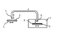
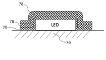
- a powder or granular material 2 whose weight per unit area is controlled to a constant level is applied to a substrate 1.
- the standard of constant weight is within ⁇ 5%, preferably within ⁇ 1.5%, of the set value per square centimeter. For example, in the case of 0.6 mg per square centimeter ⁇ 0.03 mg Or within ⁇ 0.009 mg.
- the granular material can be easily sucked by bringing the suction port 3 close to or in contact with the granular surface 2 on the base material 1.
- the granular material is transferred to the jet nozzle 5 by differential pressure via the communication channel 4 communicating from the suction port 3 and is applied to a substrate 6 such as an LED or a member for an LED to form the coating layer 8.
- the jet nozzle may be a nozzle, and the shape is round, square, slit groove, shape, size, or material regardless of the shape, but it is preferable to select according to the shape of the object to be coated such as LED or LED member.
- the coating distribution of the powder and granules 6 is equalized by applying, for example, 100 layers in multiple layers as much as possible. It can be made constant. Alternatively, it is possible to prepare a plurality of substrates coated with one or more layers and sequentially laminate them for averaging.
- the coating film weight of powder particles such as phosphors of the present invention can be improved.
- the differential pressure can be generated also by the ejector method, but negative pressure (vacuum) is applied to the application chamber 7 in which the object to be coated is installed, and a differential pressure is generated at the suction port 3 and the spout 5 to suck the granular material. Can be applied to the substrate. It is also possible to form a powder such as a phosphor while applying a collision pressure on a substrate with a differential pressure of 50 kPa or more and an ejection speed of 150 m / sec or more. In addition, 50 kPa or more means the high vacuum side more.
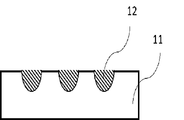
- the base 11 is provided with an uneven portion and the powder particles 12 are applied, and if necessary, the phosphor which has run out of the recess is removed.
- the plurality of concave or convex powdery particles 12 can be sucked and spot-applied to a substrate such as an LED or a member for an LED, or the operation can be repeated a plurality of times to be laminated.
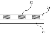
- the powder particles 22 are applied and filled in the through holes of the base 21 and the opening of the screen.
- a leakproof plate or a smaller air-permeable mesh 29 at the bottom of a substrate etc., air can be released from the mesh by spray coating etc. It is ideal by forcibly sucking the mesh 29. It can also be filled.
- the coating machine 150 may be a slurryy particle generator using ultrasonic waves or a rotary atomizer, etc., and can charge particles such as a phosphor or a substrate to form a uniform powder particle layer.
- the powder particles and the solvent may be mixed and slurryed, and the substrate may be die-coated or sprayed to coat a multilayer.
- the substrate surface can be grounded to charge the spray particles. The initial adhesion is higher when coated in a slurryy manner than when the powder is applied to the substrate, and the bulk specific gravity of the powder particles of the coating layer can be made constant.
- Spraying on a more preferable substrate is ideal because it is easier to squeeze the gas intermittently and the flow rate per unit time can be easily reduced and the coating can be thin and the coating efficiency can be enhanced.
- the solvent can be instantaneously volatilized by heating the substrate such as an LED and applying a thin layer in a pulsing manner.
- a mask 160 is placed on the base material 41 to form a powder particle pattern 42 having a desired shape and thickness.
- This method is effective because powder particles such as phosphors can be applied spot-wise to desired locations such as LEDs.
- the phosphors on the mask can be collected and reused.
- the recovered phosphor can be used as a granular material, or it can be used again as a thin film and can be laminated in a thin film in multiple layers.
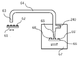
- the powder and particulate matter that has moved through the communication channel 64 as an air-water powder mixture diffuses instantaneously under vacuum at the moment when it leaves the jet port 65 in the normal channel, and energy and inertia of speed are used.
- the powder particles move toward and adhere to the tip 66 ′ on the substrate 66.
- the powder particles applied in a spot-like manner have an even smaller distance between the jet nozzle and the tip 66 'especially when the volume of the vacuum chamber is small and the volume of the vacuum pump is also small. When it approached, it had the problem of being blown off by the gas which blows off later.
- the gas has a large cross-sectional area by making the step area of the branched downstream flow channel branched upstream of the jet nozzle 65 for the purpose of preventing it smaller than the cross-sectional area of the communication flow channel preferably by half or less.
- the powder discharged from the branch port 240 has little influence on the coated powder.
- the branch port may be connected to a vacuum pump line by piping or the like because the granular material is slightly mixed into the well discharged gas not by one but by two or more.
- an object to be coated such as an LED chip is coated in advance with a binder such as silicone or a binder containing a small amount of powder particles such as phosphors, and then coated with particles such as phosphors and adhered to the binder.
- the powder can be incorporated into the binder by providing the phosphor with high speed energy. It is also possible to coat multiple layers of different or the same kind of phosphor, or to coat multiple layers of different or the same kind of phosphor and a binder.
- it is suitable to dilute with a solvent and to lower a viscosity, and to perform spray coating etc.
- Fig. 8 After forming a wall etc. by dam formation or masking around a chip such as LED, and covering a sidewall such as a filled LLED chip with a slurry such as silicone or a binder or silicone and a small amount of phosphor, Apply phosphor from above.
- the binder may be a thermosetting silicone. It is preferable to lower the viscosity by adding a slight amount of solvent in order to increase the filling property of the silicone to be filled.
- FIG. 9 is a particle size distribution of a general phosphor for LED.
- FIG. 10 is a cross-sectional view of an ejector pump type differential pressure generating means.
- the differential pressure can be easily generated by injecting compressed gas into the ejector pump 120. While the compressed gas is being injected, the suction port is at a negative pressure, and the patterned powder particles 92 on the substrate 91 are sucked and jetted from the jet port 95 via the flow path 94. If the step area of the flow path downstream of the branch is smaller than the cross-sectional area of the flow path 94 upstream of the branch, for example, half or less, the excess gas can be discharged from the branch port and there is no spatter Pattern 98 is applied.
- the number of branch ports can be two or more, and can be connected to the exhaust line by piping or the like.
- the injection time of compressed gas into the ejector may be as short as possible, for example, 20 milliseconds or less, in order to prevent the inflow of excess gas.
- FIG. 11 is a view in which the opening / closing means 130 is installed at the suction port of the basic device of FIG.
- a vacuum pump (not shown) in the vacuum chamber 107
- the suction port be closed at the moment when suction of the powder is finished.
- the spout may be closed at the moment when the spouting is finished.
- a pinch valve or the like (not shown) may be provided in the communication flow path 104 to close it.
- the flow path upstream of the injection port 105 is branched, and the step area of the flow path downstream from the branch portion is smaller than the step area upstream, and excess gas is discharged from the branch port provided in the vacuum chamber 107. It can be solved by In any case, from the viewpoint of energy saving, it is also important to always close by any one of the above-mentioned opening and closing means when not applying the granular material.
- the coating weight per unit area of powder particles such as phosphors to be applied to or coated on a substrate such as an LED can be made constant.
- the coating machine of granular material and a substrate are relatively moved, and application of a plurality of layers is performed. Specifically, the first layer is coated while the substrate is pitched to traverse the coating apparatus. Next, the phase of the pitch is shifted and the second layer, the third layer,.
- the coating apparatus may be pitch fed to traverse the substrate, or they may be alternated to pursue micro-more uniform coating weights.
- the method and means of application are not limited, but it is preferable to spray in a pulsed manner because the application efficiency to the substrate can be increased. Furthermore, if at least the coated surface of the substrate is grounded and electrostatic charges are added to the slurry to charge it for application, even fine particles can be adhered, which further increases the uniformity. It is effective to attach a solvent or the like that is easy to be charged to the particles that are hard to be charged.
- the weight per unit area and further per unit area per unit area can be made uniform in the present invention also in terms of probability.
- one suction port, one communication flow path and one jet port may be used, and when there are many types of powder particles such as phosphors, they may be laminated by another device. Furthermore, in the same kind of phosphor, if the vacuum volume is increased, it is possible to improve the application tact by providing 2 to 1,500 suction ports, communication channels and jet ports. However, in terms of total energy, the average inside diameter of the flow path is 2 millimeters or less, preferably 1.5 millimeters or less.
- the present invention is not limited to the application of a slurry consisting of powder particles such as one type of phosphor and a solvent to a substrate in multiple layers with a single applicator, but a plurality of fluorescences with a plurality of applicators. It is also possible to stack and apply body surly. Further, according to the present invention, a slurry consisting of a plurality of phosphors is applied to a plurality of substrates by a plurality of applicators, and the phosphors on each substrate are laminated and applied to an LED or an LED member in a desired order. it can.
- the suction port and the spout may be one by one or may be increased according to the desired production amount.
- a plurality of different types of phosphors can be stacked on an LED or the like to manufacture an LED.
- the lamination of the phosphors can be selected from at least red, green, yellow and blue phosphors.
- the order of application is not limited, for example, in the case where the LED is a blue light emitting LED, it is possible to sequentially stack the phosphors with the longest wavelength.
- the base material or the coating machine moves relative to one another to make the desired pitch feed, and one side is traversed to apply to the base material in a planar manner. If the pitch is offset shorter than one side of the LED and the pitch is laminated a number of times divided by the offset value, the coating distribution is more even.
- the cylinder may be rotated by using a coating machine with pitch feed and the substrate being a cylinder or a film wound around a cylinder.
- film etc. may be roll to roll and pitch feed (intermittent feed).
- the spout and the object to be coated such as LED are moved relative to each other, one of them is pitch-fed, one is traversed and applied on the surface, and the second and subsequent layers are offset to make the application of the phosphor more uniform.
- a jet nozzle with pitch feed it is preferable to use a jet nozzle with pitch feed, and a film etc. wound around a cylinder may be rotated or moved intermittently.
- the present invention can be applied to the fields of semiconductors, electronic parts, bio and pharmaceuticals where micro distribution and application of powder particles including not only LEDs but also nano-sized fine powder are required, and applied to aerosol deposition process High quality film formation can also be performed at low cost.
- electrodes such as secondary batteries such as LiB
- forming electrodes such as fuel cells, especially forming carbon electrodes in which platinum supports PEFC or DMFC delicate to the solvent or water, making electrode materials into a thick film
Abstract
Description
更に詳細には粉粒体である蛍光体のみ、または蛍光体と溶媒からなるスラーリー(Slurry)を基材、例えばステンレススティールなどの金属、金属の表面にコートした複合体、セラミックプレート、ゴムプレート、プラスチックフィルム、紙などの通気性基材等に塗布し、スラーリーの場合、揮発分を蒸発させ後、基材上の蛍光体を吸引して真空雰囲気下に配置したLEDまたはLED部材に塗布することができる。また粉粒体は基材に薄膜で均一に積層塗布し、基材上の粉粒体をエジェクター機構を利用して吸引しチューブなどの流路を経由させて被塗物に塗布することも含まれる。
LED部材とはLEDを製造する過程で使用するものであって、セラミックなどのプレート、蛍光体の転写フィルムいわゆる蛍光体シートなどを含み、特に限定されるものではない。
基材への塗布手段はディスペンサー、スロットノズル、霧化粒子施与、静電気付加霧化粒子施与、連続的又はパルス的スプレイ、静電気付加スプレイ、インクジェット、スクリーンスプレイ、スクリーンプリンティング、ロールコート方式等を含むがこれらに限定するものではない。
また基材はシートやプレート、円筒や円柱、円板、長尺のプラスチックフィルムや金属のロールストック、通気性のある無塵紙、通気性のあるフィルム、通気性のあるセラミックスプレートなどを含み寸法、形状、厚みなどその形態を問わない。特に基材に通気性があると粉粒体を吸引する際、理想的な気粉混合体として下流に移送できるので都合が良い。
その解決方法として、LEDチップの周囲にダムを形成したり、リフレクターを利用してスラーリーの充填を行っていたため、工程が複雑であるだけでなく、スラーリーの流動性を高めるためシリコーン樹脂などのバインダーを蛍光体より多くする必要があったため膜厚が必要以上に厚くなっていたため光のロスが発生し性能的に劣っていた。
また、後からシリコーン樹脂などでレンズモールドする際、モールド用シリコーン樹脂とLED周囲の蛍光体リッチ層との密着が悪くなることから、マスクを使用してLED周囲はコートしないようにしていたがマスクに付着した蛍光体は反応硬化タイプのシリコーンが含まれる為回収しての再利用は難しかった。
高い例えば0.4乃至2Torrのチャンバー内にセットした被塗物に対しガスで粉粒体を流動させ50kPa以上の差圧のエネルギーによりセラミックスなどの0.08乃至2マイクロメートル程度の微粒子を移送し被塗物に150m/秒以上のスピードで衝突させて成膜させることができるが、フルダイズ方式ゆえに粉砕や分吸器を使用しても前記ミクロンオーダーであっても前記のように小さい粒径と大きな粒径は流動挙動が違うのでミクロ的な単位面積当たりの成膜した膜厚分布問題は依然として残っていたし、蛍光体の平均粒径を15マイクロメートルにして成膜させようとすると衝突エネルギーでLEDのワイヤーなどの一部を破損させる課題をかかえていた。
当然粒度分布があるので例えば15ミクロンの平均粒径の場合粒度分布は数ミクロン乃至60ミクロンであったため、流動させた状態では粒子の濃淡があり平方センチ当たりの蛍光体重量は色温度がノーマルホワイトの場合5mg前後のごく少量の為、それが搬送される時間はミリ秒程度で移動することから単位時間当たりのバラツキが大きかった。
仮にガス量を多くし、蛍光体を希薄にして流動チャンバーで流動させると重い粒子が沈みやすく軽い粒子が浮くことから経時的に塗布量を安定させることは難しかった。
特に1層当たり少ない量を所望する場合は蛍光体を溶媒で50wt%以下好ましくは5w
t%以下になるように希釈したスラーリーを作成しパルス的スプレイ方法などで基材へ塗布を
行えば10層で平方センチメートルあたり0.1mgと驚異的な低塗布重量の粉粒体の分散層を形成できる。
溶媒を選択する必要があるが、本発明では蛍光体の性能に影響を与えなければ、有機溶剤のような溶媒、特に人体に害が少ないエタノールやその他のアルコール系溶剤、モノマー、水、それらの混合体、液化炭酸ガス、超臨界性流体、更には粘度を上げる目的で無水グリセリン等の単体または溶媒などとの混合体などを使用できる。
光体のみを吸引することができる。
粒度分布のすそ野が広い粉粒体を使用する場合は、基材に導電体を使用するか導電処理を行い、
静電気等を利用して何層も位相を変えながら塗布すると、特に超微粉まで塗布できるので塗布重量はより安定する。帯電効果を更に良好にしたい場合は、蛍光体などの粉粒体をポリマーなどでカブセル化したり蛍光体の一部に付着させることもできるし、帯電しやすい溶媒を使用することで蛍光体粒子の周囲に付着している溶媒が帯電し塗着効率が向上する。
は発明の理解を容易にするための一例にすぎず本発明の技術的思想を逸脱しない範囲にお
いて当業者により実施可能な付加、置換、変形等を施すことを排除するものではない。
例えば平方センチメートル当たり0.6mgの場合±0.03mg
または±0.009mg以内である。粉粒体は吸入口3を基材1上の粉粒体面2に近接乃至接触させることにより容易に吸引できる。
粉粒体は吸引口3から連通する連通流路4を経由して噴出口5へ差圧で移送されLEDまたはLED用部材などの被塗物6へ塗布され塗布層8を形成する。噴出口はノズルでもよく、形状は丸、四角、スリット溝など形状や大小、材質を問わないが、LEDやLED部材などの被塗物の形状に合わせて選択することが好ましい。基材上の粉粒体の単位面積当たりの重量を一定にする手段は複数層可能な限り多層に例えば100層塗布することにより粉粒体6の塗布分布は均され単位面積当たりの塗布重量を一定にすることができる。または1層あるいは複数層塗布された基材を複数用意して順に積層し平均化を図ることもできる。また噴出口5からLEDやLED部材などの被塗物6に噴出して塗布する場合も1層だけでなく単位面積当たりの重量を可能な限り少なくして薄膜で複数層積層し被塗物上の蛍光体などの粉粒体の塗膜重量を向上させることができる。基材や被塗物へ積層する場合は塗布手段と基材、更には吸引口と基材、または噴出口と被塗物を相対移動させることが好ましい。差圧はエジェクター方式でも生じさせることができるが、被塗物が設置された塗布室内7を負圧(真空)にし、吸引口3と噴出口5に差圧を発生させて粉粒体を吸引して被塗物に塗布することができる。差圧を50kPa以上にして粉粒体の噴出速度を150m/秒以上にして被塗物上に衝突塗布させながら蛍光体などの粉粒体の成膜も可能である。尚50kPa以上とはより高真空サイドの意味である。
み出した蛍光体は取り除かれる。
複数の凹部または凸の粉粒体12を吸引してLEDやLED用部材などの被塗物へスポット的に塗布し、またはその作業を複数回くり返し行い積層することができる。
どの下部に洩れ防止用プレートや蛍光体より小さい通気性のメッシュ29を置いて、スプレイ塗布などで空気をメッシュから逃がすこともできるし強制的にメッシュ29を吸引することにより理想的な充填を行うこともできる。
ン42を形成できる。この方法はLEDなどの所望する個所にスポット的に蛍光体などの粉粒体を塗布できるので効果的である。マスク上の蛍光体は回収し再利用できる。回収した蛍光体は粉粒体のまま、または再度スラーリーにして使用でき薄膜で多層に積層することができる。
2,12,22,32,42,52,62,102 基材上粉粒体(蛍光体)
3,63,93,103 吸引口
4,64,94,104 連通流路
5,65,95,105、 噴出口(孔)
6,66’、96’、106’ LEDまたはLED用部材
7,87、107 負圧(真空)室
8,68,78,88,98,108 塗布層
6,66,76、76,86,96,106 被塗物(基板)
79,89、 バインダー
140,240 分岐口
150 スプレイ装置
160 マスク
Claims (16)
- 基材上の粉粒体を吸引して移送し被塗物に噴出して塗布する方法であって、基材に少なくとも一種類の粉粒体を単位面積当たりの塗布量が均一になるように塗布する第一の工程と、基材上の粉粒体の吸引口と被塗物への粉粒体噴出口を連通する第二の工程と、前記吸引口と噴出口との間に圧力差発生手段を設ける第三の工程と、前記吸引口と基材を近接乃至接触させて前記粉粒体を吸引する第四の工程と、前記粉粒体噴出口の上流を分岐して余剰な気体を分岐口から排出しつつ、前記噴出口から粉粒体を前記被塗物へ塗布する第五の工程からなることを特徴とする粉粒体の塗布方法。
- 前記圧力差発生手段がエジェクターポンプ方式であることを特徴とする請求項1の粉粒体の塗布方法。
- 前記圧力差発生手段が少なくとも被塗物、分岐口、噴出口を真空下に配置し、差圧を発生させ被塗物に粉粒体を塗布または成膜させることを特徴とする請求項1の粉粒体の塗布方法。
- 前記基材に塗布機で粉粒体を薄膜で積層することを特徴とする請求項1の粉粒体の塗布方法。
- 前記基材への粉粒体の塗布が基材と塗布機の相対移動により行われ、1層当たりの塗布重量が平方センチメートル当たり0.01乃至5ミリグラムの薄膜であって2乃至200層積層することを特徴とする請求項4の粉粒体の塗布方法。
- 前記粉粒体が粉粒体と溶媒からなるスラーリー(Slurry)であって塗布機が粒子発生装置であって基材にスラーリーを塗布することを特徴とする請求項5の粉粒体の塗布方法。
- 前記粒子発生装置がスプレイ装置またはパルス的スプレイ発生装置であって前記基材またはスプレイ装置がピッチ送りで移動しピッチの位相を変えて積層することを特徴とする請求項6の粉粒体の塗布方法。
- 前記被塗物への粉粒体の積層が2乃至200層行われることを特徴とする請求項1の粉粒体の塗布方法。
- 基材上の粉粒体を吸引し移送し被塗物に噴出して塗布する方法であって、基材に少なくとも1種類の粉粒体を単位面積当たりの塗布量が均一になるように塗布する第一の工程と、基材上の粉粒体の吸引口と被塗物への噴出口を連通する連通流路を設ける第二の工程と、前記吸引口と噴出口の間に流路開閉手段を設ける第三の工程と、少なくとも前記被塗物と噴出口を真空下に配置し吸引口と噴出口に圧力差を設ける第四の工程と、前記開閉手段を開にして前記吸引口と基材を近接乃至接触して前記粉粒体を吸引し前記噴出口から被塗物へ粉粒体を噴出させ塗布または成膜させることを特徴とする粉粒体の塗布方法。
- 前記基材上の吸引口、被塗物上の噴出口、及び連通流路数を2乃至1500にすることを特徴とする請求項9の粉粒体の塗布方法。
- あらかじめ被塗物にバインダーを被覆することを特徴とする請求項10の粉粒体の塗布方法。
- 前記粉粒体が蛍光体であって、前記被塗物がLEDまたはLED用部材であることを特徴とする請求項1乃至11のいずれかに記載の粉粒体の塗布方法。
- 前記蛍光体を基材にパターンで塗布することを特徴とする請求項12の粉粒体の塗布方法。
- 前記バインダーがシリコーンであって前記LEDまたはLED部材の少なくとも一部にシリコーンまたはシリコーンと蛍光体からなるスラーリー(Slurry)が被覆されていることを特徴とする請求項12の粉粒体の塗布方法。
- 前記基材上の蛍光体が異なる色の蛍光体で積層されていることを特徴とする請求項12の粉粒体の塗布方法。
- 複数の基材にそれぞれが単色であって複数の色の蛍光体が塗布され、それぞれの蛍光体をLEDまたはLED用部材に積層することを特徴とする請求項12の粉粒体の塗布方法を提供する。
Priority Applications (4)
| Application Number | Priority Date | Filing Date | Title |
|---|---|---|---|
| CN202010442591.3A CN111599979B (zh) | 2014-10-18 | 2014-12-02 | 二次电池的电极形成方法 |
| KR1020167034978A KR102346145B1 (ko) | 2014-10-18 | 2014-12-02 | 분립체의 도포방법 |
| CN201480080045.2A CN106660065B (zh) | 2014-10-18 | 2014-12-02 | 粉粒体的涂布方法 |
| US15/319,870 US10625297B2 (en) | 2014-10-18 | 2014-12-02 | Method of applying powder or granular material |
Applications Claiming Priority (2)
| Application Number | Priority Date | Filing Date | Title |
|---|---|---|---|
| JP2014-213252 | 2014-10-18 | ||
| JP2014213252A JP6481154B2 (ja) | 2014-10-18 | 2014-10-18 | 粉粒体の塗布方法 |
Publications (1)
| Publication Number | Publication Date |
|---|---|
| WO2016059732A1 true WO2016059732A1 (ja) | 2016-04-21 |
Family
ID=55746299
Family Applications (1)
| Application Number | Title | Priority Date | Filing Date |
|---|---|---|---|
| PCT/JP2014/081877 WO2016059732A1 (ja) | 2014-10-18 | 2014-12-02 | 粉粒体の塗布方法 |
Country Status (5)
| Country | Link |
|---|---|
| US (1) | US10625297B2 (ja) |
| JP (1) | JP6481154B2 (ja) |
| KR (1) | KR102346145B1 (ja) |
| CN (2) | CN111599979B (ja) |
| WO (1) | WO2016059732A1 (ja) |
Families Citing this family (6)
| Publication number | Priority date | Publication date | Assignee | Title |
|---|---|---|---|---|
| EP3578374B1 (en) * | 2017-02-03 | 2023-08-30 | Hitachi Zosen Corporation | Powder film forming method and powder film forming device |
| JP2020129495A (ja) * | 2019-02-08 | 2020-08-27 | エムテックスマート株式会社 | 全固体電池の製造方法 |
| JP2021087905A (ja) * | 2019-12-02 | 2021-06-10 | エムテックスマート株式会社 | 粉粒体の塗布または成膜方法 |
| CN111668455A (zh) * | 2020-05-22 | 2020-09-15 | 宜春清陶能源科技有限公司 | 降低电池极片表面涂覆浆料过程中气泡量的方法及其在固态电解质涂布的应用 |
| JP2022007837A (ja) * | 2020-06-27 | 2022-01-13 | 正文 松永 | 粒子の製造方法、粒子またはスラリーの塗布方法、2次電池または2次電池の製造方法、全固体電池または全固体電池の製造方法、ledまたはledの製造方法、蛍光体シートまたは蛍光体シートの製造方法 |
| JP2024054597A (ja) * | 2022-10-05 | 2024-04-17 | エムテックスマート株式会社 | 粉体の塗布方法、二次電池の製造方法、全固体電池の製造方法、二次電池、全固体電池 |
Citations (4)
| Publication number | Priority date | Publication date | Assignee | Title |
|---|---|---|---|---|
| JPH07172575A (ja) * | 1993-12-17 | 1995-07-11 | Nordson Kk | 粉粒体の供給搬送方法 |
| JP2001170551A (ja) * | 1999-12-15 | 2001-06-26 | Nordson Kk | 粉体塗装における粉体の微量搬送方法 |
| JP2006313829A (ja) * | 2005-05-09 | 2006-11-16 | Konica Minolta Opto Inc | 白色発光ダイオード及びその製造方法 |
| WO2014171535A1 (ja) * | 2013-04-20 | 2014-10-23 | エムテックスマート株式会社 | 粉粒体の塗布または分配方法 |
Family Cites Families (28)
| Publication number | Priority date | Publication date | Assignee | Title |
|---|---|---|---|---|
| GB8627308D0 (en) * | 1986-11-14 | 1986-12-17 | Alcan Int Ltd | Composite metal deposit |
| US4940185A (en) * | 1988-12-09 | 1990-07-10 | Fu Hsueh Chin | Safety exhaust valve equipped spray gun |
| JP3106588B2 (ja) | 1991-09-24 | 2000-11-06 | 松下電器産業株式会社 | 濾過器 |
| JPH09184080A (ja) * | 1995-12-27 | 1997-07-15 | Vacuum Metallurgical Co Ltd | 超微粒子による薄膜形成方法、およびその薄膜形成装置 |
| US6375094B1 (en) * | 1997-08-29 | 2002-04-23 | Nordson Corporation | Spray gun handle and trigger mechanism |
| US6402500B1 (en) * | 1997-11-06 | 2002-06-11 | Matsys | Fluidized fillshoe system |
| US6630257B2 (en) * | 1998-06-10 | 2003-10-07 | U.S. Nanocorp. | Thermal sprayed electrodes |
| JP2000301052A (ja) * | 1999-04-16 | 2000-10-31 | Anest Iwata Corp | 粉体塗料の定量供給方法 |
| US6576488B2 (en) * | 2001-06-11 | 2003-06-10 | Lumileds Lighting U.S., Llc | Using electrophoresis to produce a conformally coated phosphor-converted light emitting semiconductor |
| US6875278B2 (en) * | 2001-09-07 | 2005-04-05 | Material Sciences Corporation | Modular powder application system |
| ATE525755T1 (de) * | 2001-10-12 | 2011-10-15 | Nichia Corp | Lichtemittierendes bauelement und verfahren zu seiner herstellung |
| JP3863029B2 (ja) * | 2002-02-07 | 2006-12-27 | 大成化工株式会社 | 肩部を有する容器内面への粉体塗装装置並びに粉体塗装方法 |
| DE10224780A1 (de) * | 2002-06-04 | 2003-12-18 | Linde Ag | Verfahren und Vorrichtung zum Kaltgasspritzen |
| WO2005025787A1 (ja) * | 2003-09-12 | 2005-03-24 | National Institute Of Advanced Industrial Science And Technology | 微細な液滴の形状で噴射し、積層塗布可能な金属ナノ粒子分散液 |
| BRPI0511950A (pt) * | 2004-06-10 | 2008-01-29 | California Inst Of Techn | métodos de produzir um material de eletrólito para uma célula de combustìvel de ácido sólido e de depositar um eletrólito sobre um substrato, célula de combustìvel, e, métodos de preparar partìculas de uma camada de eletrocatalisador para uma célula de combustìvel de ácido sólido, de depositar um eletrocatalisador sobre um substrato e de selar uma célula de combustìvel |
| JP2007050371A (ja) * | 2005-08-19 | 2007-03-01 | Matsushita Electric Ind Co Ltd | 標準粒子塗布装置及び標準粒子塗布方法 |
| US20080020923A1 (en) * | 2005-09-13 | 2008-01-24 | Debe Mark K | Multilayered nanostructured films |
| JP2009028709A (ja) * | 2007-06-29 | 2009-02-12 | Brother Ind Ltd | エアロゾル生成装置およびエアロゾル生成方法 |
| JP4687695B2 (ja) * | 2007-07-23 | 2011-05-25 | トヨタ自動車株式会社 | 膜電極接合体製造方法 |
| JP2009101285A (ja) * | 2007-10-23 | 2009-05-14 | Nidec-Kyori Corp | 液体塗布装置 |
| US9099738B2 (en) * | 2008-11-03 | 2015-08-04 | Basvah Llc | Lithium secondary batteries with positive electrode compositions and their methods of manufacturing |
| EP2218514B1 (de) * | 2009-02-09 | 2017-04-26 | J. Wagner AG | Beschichtungspulver-Versorgungs-vorrichtung |
| US9676955B2 (en) * | 2011-08-31 | 2017-06-13 | Sumitomo Chemical Company, Limited | Coating liquid, laminated porous film, and method for producing laminated porous film |
| CN103084315A (zh) * | 2011-10-30 | 2013-05-08 | 湖南晟通科技集团有限公司 | 一种阳极钢爪的石墨糊喷涂物及其喷涂方法 |
| WO2013089075A1 (ja) * | 2011-12-13 | 2013-06-20 | 東レ株式会社 | 積層体および波長変換層付き発光ダイオードの製造方法 |
| WO2013096220A1 (en) * | 2011-12-20 | 2013-06-27 | Applied Materials, Inc. | Apparatus and method for hot coating electrodes of lithium-ion batteries |
| JP5840959B2 (ja) | 2012-01-16 | 2016-01-06 | エムテックスマート株式会社 | 塗布方法及び装置 |
| CN103817052B (zh) * | 2014-02-21 | 2016-06-22 | 华南理工大学 | 全自动led荧光粉涂覆设备及其控制方法 |
-
2014
- 2014-10-18 JP JP2014213252A patent/JP6481154B2/ja active Active
- 2014-12-02 CN CN202010442591.3A patent/CN111599979B/zh active Active
- 2014-12-02 KR KR1020167034978A patent/KR102346145B1/ko active IP Right Grant
- 2014-12-02 CN CN201480080045.2A patent/CN106660065B/zh active Active
- 2014-12-02 US US15/319,870 patent/US10625297B2/en active Active
- 2014-12-02 WO PCT/JP2014/081877 patent/WO2016059732A1/ja active Application Filing
Patent Citations (4)
| Publication number | Priority date | Publication date | Assignee | Title |
|---|---|---|---|---|
| JPH07172575A (ja) * | 1993-12-17 | 1995-07-11 | Nordson Kk | 粉粒体の供給搬送方法 |
| JP2001170551A (ja) * | 1999-12-15 | 2001-06-26 | Nordson Kk | 粉体塗装における粉体の微量搬送方法 |
| JP2006313829A (ja) * | 2005-05-09 | 2006-11-16 | Konica Minolta Opto Inc | 白色発光ダイオード及びその製造方法 |
| WO2014171535A1 (ja) * | 2013-04-20 | 2014-10-23 | エムテックスマート株式会社 | 粉粒体の塗布または分配方法 |
Also Published As
| Publication number | Publication date |
|---|---|
| US20170136492A1 (en) | 2017-05-18 |
| JP2016077982A (ja) | 2016-05-16 |
| KR20170072833A (ko) | 2017-06-27 |
| CN111599979A (zh) | 2020-08-28 |
| CN106660065A (zh) | 2017-05-10 |
| US10625297B2 (en) | 2020-04-21 |
| CN106660065B (zh) | 2020-09-22 |
| CN111599979B (zh) | 2022-11-18 |
| JP6481154B2 (ja) | 2019-03-13 |
| KR102346145B1 (ko) | 2021-12-30 |
Similar Documents
| Publication | Publication Date | Title |
|---|---|---|
| WO2016059732A1 (ja) | 粉粒体の塗布方法 | |
| JP6328104B2 (ja) | 粉粒体の塗布方法 | |
| WO2020162284A1 (ja) | 全固体電池の製造方法 | |
| US20140004260A1 (en) | Deposition method | |
| JP2022172307A (ja) | 全固体電池の製造方法 | |
| JP2016077982A5 (ja) | ||
| WO2020145214A1 (ja) | 全固体電池の製造方法 | |
| WO2016006120A1 (ja) | Ledの製造方法及びled | |
| WO2021111947A1 (ja) | 粉粒体の塗布または成膜方法 | |
| JP2021118062A (ja) | 2次電池の製造方法または2次電池 | |
| JP6233872B2 (ja) | Ledの製造方法 | |
| JP7123398B2 (ja) | 流体エジェクタ | |
| JP6507434B2 (ja) | Ledの製造方法及びled | |
| WO2021261506A1 (ja) | 粒子の製造方法、粒子またはスラリーの塗布方法、2次電池または2次電池の製造方法、全固体電池または全固体電池の製造方法、ledまたはledの製造方法、蛍光体シートまたは蛍光体シートの製造方法 | |
| WO2022049974A1 (ja) | 塗布方法、燃料電池の製造方法または燃料電池、2次電池の製造方法または2次電池、全固体電池の製造方法または全固体電池 | |
| WO2023042765A1 (ja) | 電池の電極形成方法、膜電極アッセンブリーの製造方法、膜電極アッセンブリー、燃料電池または水電解水素発生装置 | |
| JP2022047612A (ja) | 塗布方法、燃料電池の製造方法または燃料電池、2次電池の製造方法または2次電池、全固体電池の製造方法または全固体電池 | |
| KR20080049980A (ko) | 정전 분무 코팅 장치 및 방법 |
Legal Events
| Date | Code | Title | Description |
|---|---|---|---|
| 121 | Ep: the epo has been informed by wipo that ep was designated in this application |
Ref document number: 14904112 Country of ref document: EP Kind code of ref document: A1 |
|
| ENP | Entry into the national phase |
Ref document number: 20167034978 Country of ref document: KR Kind code of ref document: A |
|
| WWE | Wipo information: entry into national phase |
Ref document number: 15319870 Country of ref document: US |
|
| NENP | Non-entry into the national phase |
Ref country code: DE |
|
| 122 | Ep: pct application non-entry in european phase |
Ref document number: 14904112 Country of ref document: EP Kind code of ref document: A1 |