WO2016056320A1 - 半導体装置及びバスバー - Google Patents
半導体装置及びバスバー Download PDFInfo
- Publication number
- WO2016056320A1 WO2016056320A1 PCT/JP2015/074456 JP2015074456W WO2016056320A1 WO 2016056320 A1 WO2016056320 A1 WO 2016056320A1 JP 2015074456 W JP2015074456 W JP 2015074456W WO 2016056320 A1 WO2016056320 A1 WO 2016056320A1
- Authority
- WO
- WIPO (PCT)
- Prior art keywords
- semiconductor
- bus bar
- terminal
- inductance
- resistance
- Prior art date
- Legal status (The legal status is an assumption and is not a legal conclusion. Google has not performed a legal analysis and makes no representation as to the accuracy of the status listed.)
- Ceased
Links
Images



Classifications
-
- H—ELECTRICITY
- H05—ELECTRIC TECHNIQUES NOT OTHERWISE PROVIDED FOR
- H05K—PRINTED CIRCUITS; CASINGS OR CONSTRUCTIONAL DETAILS OF ELECTRIC APPARATUS; MANUFACTURE OF ASSEMBLAGES OF ELECTRICAL COMPONENTS
- H05K7/00—Constructional details common to different types of electric apparatus
- H05K7/02—Arrangements of circuit components or wiring on supporting structure
- H05K7/026—Multiple connections subassemblies
-
- H—ELECTRICITY
- H02—GENERATION; CONVERSION OR DISTRIBUTION OF ELECTRIC POWER
- H02B—BOARDS, SUBSTATIONS OR SWITCHING ARRANGEMENTS FOR THE SUPPLY OR DISTRIBUTION OF ELECTRIC POWER
- H02B1/00—Frameworks, boards, panels, desks, casings; Details of substations or switching arrangements
- H02B1/20—Bus-bar or other wiring layouts, e.g. in cubicles, in switchyards
- H02B1/205—Bus-bar or other wiring layouts, e.g. in cubicles, in switchyards for connecting electrical apparatus mounted side by side on a rail
-
- H—ELECTRICITY
- H05—ELECTRIC TECHNIQUES NOT OTHERWISE PROVIDED FOR
- H05K—PRINTED CIRCUITS; CASINGS OR CONSTRUCTIONAL DETAILS OF ELECTRIC APPARATUS; MANUFACTURE OF ASSEMBLAGES OF ELECTRICAL COMPONENTS
- H05K7/00—Constructional details common to different types of electric apparatus
- H05K7/02—Arrangements of circuit components or wiring on supporting structure
- H05K7/06—Arrangements of circuit components or wiring on supporting structure on insulating boards, e.g. wiring harnesses
-
- H—ELECTRICITY
- H05—ELECTRIC TECHNIQUES NOT OTHERWISE PROVIDED FOR
- H05K—PRINTED CIRCUITS; CASINGS OR CONSTRUCTIONAL DETAILS OF ELECTRIC APPARATUS; MANUFACTURE OF ASSEMBLAGES OF ELECTRICAL COMPONENTS
- H05K7/00—Constructional details common to different types of electric apparatus
- H05K7/14—Mounting supporting structure in casing or on frame or rack
- H05K7/1422—Printed circuit boards receptacles, e.g. stacked structures, electronic circuit modules or box like frames
- H05K7/1427—Housings
- H05K7/1432—Housings specially adapted for power drive units or power converters
- H05K7/14329—Housings specially adapted for power drive units or power converters specially adapted for the configuration of power bus bars
-
- H—ELECTRICITY
- H10—SEMICONDUCTOR DEVICES; ELECTRIC SOLID-STATE DEVICES NOT OTHERWISE PROVIDED FOR
- H10W—GENERIC PACKAGES, INTERCONNECTIONS, CONNECTORS OR OTHER CONSTRUCTIONAL DETAILS OF DEVICES COVERED BY CLASS H10
- H10W70/00—Package substrates; Interposers; Redistribution layers [RDL]
- H10W70/60—Insulating or insulated package substrates; Interposers; Redistribution layers
- H10W70/611—Insulating or insulated package substrates; Interposers; Redistribution layers for connecting multiple chips together
-
- H—ELECTRICITY
- H10—SEMICONDUCTOR DEVICES; ELECTRIC SOLID-STATE DEVICES NOT OTHERWISE PROVIDED FOR
- H10W—GENERIC PACKAGES, INTERCONNECTIONS, CONNECTORS OR OTHER CONSTRUCTIONAL DETAILS OF DEVICES COVERED BY CLASS H10
- H10W70/00—Package substrates; Interposers; Redistribution layers [RDL]
- H10W70/60—Insulating or insulated package substrates; Interposers; Redistribution layers
- H10W70/62—Insulating or insulated package substrates; Interposers; Redistribution layers characterised by their interconnections
- H10W70/63—Vias, e.g. via plugs
- H10W70/635—Through-vias
-
- H—ELECTRICITY
- H10—SEMICONDUCTOR DEVICES; ELECTRIC SOLID-STATE DEVICES NOT OTHERWISE PROVIDED FOR
- H10W—GENERIC PACKAGES, INTERCONNECTIONS, CONNECTORS OR OTHER CONSTRUCTIONAL DETAILS OF DEVICES COVERED BY CLASS H10
- H10W70/00—Package substrates; Interposers; Redistribution layers [RDL]
- H10W70/60—Insulating or insulated package substrates; Interposers; Redistribution layers
- H10W70/62—Insulating or insulated package substrates; Interposers; Redistribution layers characterised by their interconnections
- H10W70/65—Shapes or dispositions of interconnections
- H10W70/658—Shapes or dispositions of interconnections for devices provided for in groups H10D8/00 - H10D48/00
-
- H—ELECTRICITY
- H10—SEMICONDUCTOR DEVICES; ELECTRIC SOLID-STATE DEVICES NOT OTHERWISE PROVIDED FOR
- H10W—GENERIC PACKAGES, INTERCONNECTIONS, CONNECTORS OR OTHER CONSTRUCTIONAL DETAILS OF DEVICES COVERED BY CLASS H10
- H10W70/00—Package substrates; Interposers; Redistribution layers [RDL]
- H10W70/60—Insulating or insulated package substrates; Interposers; Redistribution layers
- H10W70/67—Insulating or insulated package substrates; Interposers; Redistribution layers characterised by their insulating layers or insulating parts
- H10W70/68—Shapes or dispositions thereof
- H10W70/685—Shapes or dispositions thereof comprising multiple insulating layers
-
- H—ELECTRICITY
- H10—SEMICONDUCTOR DEVICES; ELECTRIC SOLID-STATE DEVICES NOT OTHERWISE PROVIDED FOR
- H10W—GENERIC PACKAGES, INTERCONNECTIONS, CONNECTORS OR OTHER CONSTRUCTIONAL DETAILS OF DEVICES COVERED BY CLASS H10
- H10W72/00—Interconnections or connectors in packages
-
- H—ELECTRICITY
- H10—SEMICONDUCTOR DEVICES; ELECTRIC SOLID-STATE DEVICES NOT OTHERWISE PROVIDED FOR
- H10W—GENERIC PACKAGES, INTERCONNECTIONS, CONNECTORS OR OTHER CONSTRUCTIONAL DETAILS OF DEVICES COVERED BY CLASS H10
- H10W90/00—Package configurations
-
- H—ELECTRICITY
- H02—GENERATION; CONVERSION OR DISTRIBUTION OF ELECTRIC POWER
- H02M—APPARATUS FOR CONVERSION BETWEEN AC AND AC, BETWEEN AC AND DC, OR BETWEEN DC AND DC, AND FOR USE WITH MAINS OR SIMILAR POWER SUPPLY SYSTEMS; CONVERSION OF DC OR AC INPUT POWER INTO SURGE OUTPUT POWER; CONTROL OR REGULATION THEREOF
- H02M7/00—Conversion of AC power input into DC power output; Conversion of DC power input into AC power output
- H02M7/003—Constructional details, e.g. physical layout, assembly, wiring or busbar connections
-
- H—ELECTRICITY
- H05—ELECTRIC TECHNIQUES NOT OTHERWISE PROVIDED FOR
- H05K—PRINTED CIRCUITS; CASINGS OR CONSTRUCTIONAL DETAILS OF ELECTRIC APPARATUS; MANUFACTURE OF ASSEMBLAGES OF ELECTRICAL COMPONENTS
- H05K2201/00—Indexing scheme relating to printed circuits covered by H05K1/00
- H05K2201/10—Details of components or other objects attached to or integrated in a printed circuit board
- H05K2201/10227—Other objects, e.g. metallic pieces
- H05K2201/10272—Busbars, i.e. thick metal bars mounted on the printed circuit board [PCB] as high-current conductors
Definitions
- the present invention relates to a semiconductor device and a bus bar.
- the present invention has been made in view of these points, and an object thereof is to provide a semiconductor device in which a difference in current with respect to a semiconductor module is reduced.
- a plurality of semiconductor modules having a semiconductor element, a main terminal led out to the outside, a wiring portion connecting the semiconductor element and the main terminal, one terminal part, A plurality of mounting portions connected to the main terminal, and including one or more bus bars for connecting the semiconductor modules in parallel, and most of the resistance between the terminal portion and each of the mounting portions A semiconductor in which a large resistance is 10% or less of the resistance of the wiring portion, and the largest inductance among the inductances between the terminal portion and each of the mounting portions is 10% or less of the inductance of the wiring portion.
- a bus bar having one terminal portion and a plurality of attachment portions, and connecting a plurality of semiconductor modules in parallel at the attachment portion, each of the terminal portions and The difference between the largest resistance and the smallest resistance among the resistances of the mounting part is 25 n ⁇ or less, and other bus bars connecting the semiconductor modules in parallel are arranged in parallel with a spacing of 1 mm or less.
- a bus bar is provided in which the difference between the largest inductance and the smallest inductance among the inductances of the terminal portions and the respective attachment portions is 2 nH or less.
- 1 is a diagram illustrating a semiconductor device according to a first embodiment.
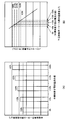
- 4 is a graph showing a temperature difference between a semiconductor element and a case and a power cycle life of the first embodiment. It is a figure which shows the semiconductor module of 2nd Embodiment. It is a perspective view which shows the semiconductor device of 2nd Embodiment. It is a figure which shows the bus bar of 2nd Embodiment. It is a figure for demonstrating the bus bar which connects a semiconductor module in parallel in 2nd Embodiment. It is a figure which shows the circuit comprised with the semiconductor device of 2nd Embodiment.
- FIG. 1 is a diagram illustrating the semiconductor device according to the first embodiment.
- the semiconductor device 10 includes a plurality of semiconductor modules 1 and 2 and bus bars 3 and 4 that electrically connect the plurality of semiconductor modules 1 and 2 in parallel.
- two or more semiconductor modules can be electrically connected by the bus bars 3 and 4.
- the first embodiment a case where two semiconductor modules 1 and 2 are used will be described.
- the semiconductor module 1 includes a semiconductor element 1a, main terminals 1b and 1d led to the outside, and wiring portions 1c and 1e.
- the semiconductor module 2 includes a semiconductor element 2a, main terminals 2b and 2d led to the outside, and wiring portions 2c and 2e.
- the semiconductor elements 1a and 2a are, for example, power semiconductors. Specifically, it is configured by one or a plurality of IGBTs, FWDs, power MOSFETs (Metal / Oxide / Semiconductor / Field / Effect / Transistors), or the like.
- each of the wiring portions 1c, 1e, 2c, 2e has a resistance Ri and an inductance Li.
- the resistance Ri of the wiring portions 1c, 1e, 2c, and 2e may be referred to as the internal resistance of the semiconductor modules 1 and 2, and the inductance Li of the wiring portions 1c, 1e, 2c, and 2e is the semiconductor module 1, 2. May be referred to as internal inductance.
- the bus bar 3 is connected to the main terminal 1b of the semiconductor module 1 at the attachment portion 3b1, and is connected to the main terminal 2b of the semiconductor module 2 at the attachment portion 3b2.
- the bus bar 4 is connected to the main terminal 1d of the semiconductor module 1 at the attachment portion 4b1, and is connected to the main terminal 2d of the semiconductor module 2 at the attachment portion 4b2.
- the terminal portion 3a of the bus bar 3 and the terminal portion 4a of the bus bar 4 are connected to an external power source (not shown).
- a resistance Rm1 and an inductance Lm1 are inherent to the flowing current.
- the resistance and inductance between the terminal portion 3a and the mounting portion 3b2 of the bus bar 3 are assumed to be negligibly small. That is, the largest resistance among the resistances between the terminal portion 3a and the attachment portions 3b1 and 3b2 is the resistance Rm1.
- the largest inductance is the inductance Lm1.
- a resistor Rm2 and an inductance Lm2 are inherent between the terminal portion 4a and the mounting portion 4b1 of the bus bar 4. And as with the bus bar 3, the largest resistance among the resistances between the terminal part 4a and the attachment parts 4b1 and 4b2 is the resistance Rm2. Of the inductances between the terminal portion 4a and the mounting portions 4b1, 4b2, the largest inductance is the inductance Lm2.
- the largest resistances Rm1 and Rm2 among the resistances between the terminal portions 3a and 4a of the bus bars 3 and 4 and the mounting portions 3b1, 3b2, 4b1 and 4b2 are the semiconductor module 1.
- 2 is 10% or less of the resistance Ri of the wiring portions 1c, 1e, 2c, 2e.
- the largest inductances Lm1, Lm2 are the wiring portions 1c, 1e, It is 10% or less of the inductance Li of 2c and 2e.
- the semiconductor element 1a of the semiconductor module 1 is connected to a resistance obtained by combining the two resistances Ri of the wiring portions 1c and 1e and the resistances Rm1 and Rm2 of the bus bars 3 and 4.
- an inductance obtained by combining the two inductances Li of the wiring portions 1c and 1e and the inductances Lm1 and Lm2 of the bus bars 3 and 4 is connected to the semiconductor element 1a.
- the semiconductor element 2a of the semiconductor module 2 is connected to a resistance that is a combination of the two resistances Ri of the wiring portions 2c and 2e.
- the semiconductor element 2a is connected to an inductance that is a combination of the two inductances Li of the wiring portions 2c and 2e.
- the resistance of the semiconductor module 1 is increased by the sum of the resistance Rm1 and the resistance Rm2 as compared with the semiconductor module 2.
- the inductance of the semiconductor module 1 is larger than that of the semiconductor module 2 by the sum of the inductance Lm1 and the inductance Lm2.
- the influence of the resistances Rm1 and Rm2 and the inductances Lm1 and Lm2 of the bus bars 3 and 4 becomes remarkable. That is, in the semiconductor module 1, the flowing current becomes smaller than the current of the semiconductor module 2 in accordance with the increase in the resistances Rm 1 and Rm 2 and the inductances Lm 1 and Lm 2.
- the bus bars 3 and 4 connecting the semiconductor modules 1 and 2 are arranged in parallel and the influence of the inductances Lm1 and Lm2 of the bus bars 3 and 4 can be reduced, the resistances Rm1 and Rm2 of the bus bars 3 and 4 can be reduced. It is difficult to reduce the effects of For this reason, in the semiconductor module 1, the flowing current is smaller than the current of the semiconductor module 2 due to the influence of the resistors Rm 1 and Rm 2 of the bus bars 3 and 4.
- the resistors Rm1 and Rm2 are set to 10% or less of the resistor Ri, and the inductances Lm1 and Lm2 are set to 10% or less of the inductance Li. For this reason, in the semiconductor device 10, the influence by resistance Rm1, Rm2 of bus bar 3, 4 and inductance Lm1, Lm2 is reduced.
- FIG. 2 is a graph showing the temperature difference between the semiconductor element and the case and the power cycle life of the first embodiment.
- the horizontal axis represents the current difference (%) between the semiconductor element 1a and the semiconductor element 2a
- the vertical axis represents the difference between the semiconductor element 2a and the case in the semiconductor module 2 where the temperature is higher.
- the relative value of the temperature difference ⁇ Tj is shown.
- the vertical axis indicates ⁇ Tj when the difference in current between the semiconductor element 1a and the semiconductor element 2a is 0% (that is, there is no difference in current between the semiconductor element 1a and the semiconductor element 2a) as a reference (100%). Yes.
- the horizontal axis indicates the relative value of ⁇ Tj
- the vertical axis indicates the logarithm of the relative value of the power cycle life (cycle) of the semiconductor element 2a with respect to the semiconductor element 1a.
- the vertical axis is based on the power cycle life (100%) when the difference in current between the semiconductor element 1a and the semiconductor element 2a is 0%.
- evaluation of FIG. 2 (A) is performed as follows. By supplying a current to the semiconductor elements 1a and 2a to be evaluated and changing the current value, a difference in current between the semiconductor element 1a and the semiconductor element 2a is obtained.
- the semiconductor elements 1a and 2a have a rated voltage of 1200V and a rated current of 100A.
- the power supply connected to the semiconductor elements 1a and 2a has a voltage of 600 V, a frequency of 15 kHz, and a power factor of 0.9.
- the ratio of the current difference between the semiconductor element 1a and the semiconductor element 2a is set to 0%, 5%, 10%, 15%, and 20%, and the current flowing through the semiconductor element 2a is a reference value (0%). Then, the temperature difference ⁇ Tj from the case of the semiconductor element 2a when increased by 5%, 10%, 15%, and 20% is measured.
- the temperature difference ⁇ Tj increases as the current difference between the semiconductor element 1a and the semiconductor element 2a increases. That is, the temperature of the semiconductor element 2a is increased as compared with the semiconductor element 1a.
- the difference in current between the semiconductor module 1 and the semiconductor module 2 can be reduced. It can. That is, it can be said that the difference in current between the semiconductor element 1a and the semiconductor element 2a increases as the ratio of the resistances Rm1, Rm2 (inductances Lm1, Lm2) to the resistance Ri (inductance Li) increases. Therefore, from FIG. 2A, it is considered that the temperature difference ⁇ Tj increases as the resistances Rm1, Rm2 (inductances Lm1, Lm2) increase.
- the power cycle life (cycle) of the semiconductor element 1a at each temperature difference ⁇ Tj shown in FIG. According to the graph of FIG. 2B showing the evaluation results, it is recognized that the power cycle life of the semiconductor element 2a is reduced as the temperature difference ⁇ Tj increases.
- Each temperature difference ⁇ Tj corresponds to the difference in current between the semiconductor element 1a and the semiconductor element 2a shown in FIG. That is, this evaluation result indicates that the power cycle life of the semiconductor element 2a is reduced as the difference in current between the semiconductor element 1a and the semiconductor element 2a increases.
- the power cycle life is reduced to about 1/4 (23.9%) as compared with the case where the current difference is 0%. is doing. Further, when the current difference is 15%, the power cycle life is reduced to about 1/8 (12.6%) as compared with the case where the current difference is 0%.
- the power cycle life of the semiconductor element 2a is allowed to fall to about 1/5 that of the semiconductor element 1a. For this reason, what is necessary is just to make the ratio of the difference of the electric current between the semiconductor element 1a and the semiconductor element 2a 10% or less.
- I2 ((Rm1 + Rm2) / 2Ri) * I1 (1) That is, the difference in current between the semiconductor element 1a and the semiconductor element 2a is the resistance of the bus bar 3 and the bus bar 4 with respect to the total resistance 2Ri of the wiring portions 1c, 1e, 2c, and 2e of the semiconductor modules 1 and 2. It is equal to the ratio of the total value Rm1 + Rm2.
- the bus bar 3 with respect to the resistance (2Ri) of the wiring portions 1c, 1e, 2c, 2e of the semiconductor modules 1, 2 is used.
- 4 (Rm1 + Rm2) should be 10% or less.
- the inductance (Lm1 + Lm2) of the bus bars 3 and 4 is 10% with respect to the inductance (2Li) of the wiring portion of the semiconductor module. The following should be done.
- the power of the semiconductor element 2a is reduced. Since the cycle life can be reduced to about 1 ⁇ 2 of the semiconductor element 1a, it is more preferable.
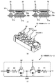
- FIG. 3 is a diagram illustrating an example of a semiconductor module according to the second embodiment.
- 3A is a side view of the configuration included in the semiconductor module 50
- FIG. 3B is a perspective view of the semiconductor module 50
- FIG. 3C is a circuit diagram of the semiconductor module 50. Each is shown.
- the semiconductor module 50 includes semiconductor chips 53a and 53b, insulating substrates 52a and 52b, conductive posts 54, a printed circuit board 55, and terminals 56 to 59.
- the semiconductor chips 53a and 53b are power semiconductors such as IGBTs, power MOSFETs, and FWDs.
- IGBTs power semiconductors
- MOSFETs power MOSFETs
- FWDs FWDs.
- FIG. 3A only one semiconductor chip 53a, 53b is displayed on each of the insulating substrates 52a, 52b.
- a switching device such as an IGBT and an FWD are arranged on the circuit board on the front surface side of each of the insulating substrates 52a and 52b, and the equivalent circuit shown in FIG. 3C is configured.
- the insulating substrates 52a and 52b are composed of a ceramic plate made of alumina or the like having good heat conductivity, and a circuit plate and a metal plate made of a conductive material such as copper disposed on the front and back surfaces thereof. A predetermined circuit pattern is formed on the circuit board on the front surface side.
- the insulating substrates 52a and 52b are, for example, a DCB (Direct Copper Bonding) substrate or an AMB (Active Metal Blazing) substrate. As shown in FIG. 3A, copper plates 51a and 51b that enhance heat dissipation may be disposed between the insulating substrates 52a and 52b and the semiconductor chips 53a and 53b.
- the printed circuit board 55 is disposed to face the circuit boards of the insulating substrates 52a and 52b.
- the printed circuit board 55 has a metal layer for wiring.
- One of the cylindrical conductive posts 54 is connected to the metal layer of the printed board 55, and the other is connected to the semiconductor chips 53a and 53b and the circuit boards of the insulating boards 52a and 52b.
- the insulating substrates 51a and 51b, the printed circuit board 55, and the conductive posts 54 are used in the wiring portion of the semiconductor module 50.
- bonding wires are often used in the wiring portion.
- the cross-sectional area of the wiring can be increased compared to the bonding wire, and the resistance and inductance of the wiring portion can be reduced. Can do.
- the inductance of a wiring part can further be reduced by arrange
- the semiconductor module 50 includes a switching device (hereinafter simply referred to as a transistor) Q1 and an FWD (hereinafter referred to as a diode) D1, an antiparallel circuit, a transistor Q2 and a diode D2. Are connected in series. Furthermore, the wiring of the above circuit has internal resistances R1, R2 and internal inductances L1, L2.
- the semiconductor chips 53a and 53b disposed on the insulating substrates 52a and 52b may equivalently constitute an antiparallel circuit of the transistors Q1 and Q2 and the diodes D1 and D2 shown in FIG. For this reason, the transistors Q1 and Q2 and the diodes D1 and D2 may be mounted with a plurality of semiconductor chips having the same rating.
- the collector electrode of the transistor Q1 is disposed on the lower surface of the semiconductor chip 53a, and the terminal 56, which is the collector terminal C1 of the semiconductor module 50, is connected via a circuit board.
- the collector electrode of the transistor Q2 disposed on the back surface of the other semiconductor chip 53b is also connected to a terminal 58 which is a collector / emitter terminal C2 / E1 through a circuit board.
- the emitter electrodes and gate electrodes of the transistors Q1 and Q2 are disposed on the front surfaces of the semiconductor chips 53a and 53b, and are connected to the printed circuit board 55 via the conductive posts 54, respectively.
- the emitter electrode of the transistor Q1 is connected to the terminal 58 via the conductive post 54 and the printed board 55
- the emitter electrode of the transistor Q2 is connected to the terminal 57 which is the emitter terminal E2 via the conductive post and the printed board 55. ing.
- the terminals 56 to 58 are disposed so as to face the semiconductor module 50 two by two as shown in FIG.
- the semiconductor module 50 further includes four terminals 59 whose tips protrude. Two of these terminals 59 are gate terminals G1 and G2 for supplying a gate control signal to the gate electrodes of the transistors Q1 and Q2 of the half-bridge circuit, and are connected to the printed circuit board 55.
- the remaining two are control (auxiliary) terminals, which are inspection terminals (not shown in FIG. 3C) for outputting a sense signal for sensing a current flowing between the collector and emitter of the transistors Q1 and Q2. It is composed. That is, the terminals 56 to 58 are main terminals through which the main current of the semiconductor module 50 flows, and the terminal 59 is a control terminal for controlling the semiconductor module 50.
- Each component of the semiconductor module 50 is molded and protected by a thermosetting resin such as an epoxy resin, for example.
- the semiconductor module 50 is a rectangular parallelepiped as shown in FIG. Ends of the ten terminals 56 to 59 protrude from the upper surface of the semiconductor module 50.
- copper plates 51c and 51d are arranged so as to be flush with the metal plates on the bottom surface side of the insulating substrates 52 and 53, respectively.
- FIG. 4 is a perspective view showing a semiconductor device according to the second embodiment.
- the semiconductor modules 50a to 50e shown in FIG. 4 have the same configuration as the semiconductor module 50.
- the semiconductor module 50 is a general term for the semiconductor modules 50a to 50e.
- the semiconductor device 100 includes five semiconductor modules 50a to 50e arranged in the same direction.
- the bus bar 60 that electrically connects the terminals 56 that are the main terminals of the semiconductor modules 50a to 50e and the terminal 57 that is the main terminal of each of the semiconductor modules 50a to 50e are electrically connected.
- a bus bar 80 that electrically connects the terminals 58 that are the main terminals of the semiconductor modules 50a to 50e.
- the bus bars 60, 70, and 80 are each provided with a terminal portion 63 (P terminal) provided with round holes 64, 74, and 84, a terminal portion 73 (N terminal), and a terminal portion 83 (AC terminal).
- a power source is connected to the terminal portions 63, 73, 83 from the outside.
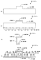
- FIG. 5 is a diagram illustrating a bus bar according to the second embodiment. 5 illustrates the bus bar 60, FIG. 5 (A) is a front view, FIG. 5 (B) is a back view opposite to FIG. 5 (A), and FIG. 5 (C). FIG. 5D shows a side view, and FIG. 5D shows a top view.
- the bus bar 60 includes a plate portion 61 having a convex portion 62, a terminal portion 63 provided at the tip of the convex portion 62, and a plurality of attachment portions 65 provided on the lower end side of the plate portion 61.
- the terminal portion 63 is provided with a round hole 64
- the attachment portion 65 is provided with a round hole 66. Further, the terminal portion 63 and the attachment portion 65 are disposed substantially at right angles to the plate portion 61.
- the bus bars 70 and 80 are the same as the bus bar 60 except that the positions of the convex portions and the terminal portions are different as shown in FIG. Then, the terminals 56 of the five semiconductor modules 50a to 50e arranged are inserted into the corresponding round holes 66 of the mounting portion 65 of the bus bar 60 and protruded. The terminal 56 protruding from the round hole 66 is soldered to the mounting portion 65, and the bus bar 60 and the semiconductor modules 50a to 50e are electrically connected. Similarly, the bus bars 70 and 80 are connected to the terminals 57 and 58 of the semiconductor modules 50a to 50e, and the semiconductor device 100 is configured.
- FIG. 6 is a diagram for explaining a bus bar for connecting semiconductor modules in parallel in the second embodiment.
- resistors R11, R13, R15, R17 and inductances L11, L13, L15, L17 are inherent.
- the terminal portion 63 of the bus bar 60 is connected between the resistor R13 and the resistor R15, and the resistance and inductance between the terminal portion 63 and the mounting portion of the semiconductor module 50c are so small that they can be ignored.
- the bus bar 70 also has a resistance and an inductance between the semiconductor modules 50.
- the bus bars 60 and 70 are made of a conductive material such as a copper alloy, for example.
- the bus bars 60 and 70 are selected to have a size (length, height, thickness) such that their resistance and inductance are as small as possible.
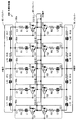
- FIG. 7 is a diagram illustrating a circuit including the semiconductor device according to the second embodiment.
- Semiconductor modules 50a to 50e are connected to the semiconductor device 100 in parallel.
- the collector terminals C1 of the semiconductor modules 50a to 50e are connected by the bus bar 60, respectively.
- the emitter terminals E2 of the semiconductor modules 50a to 50e are connected by the bus bar 70, respectively. Further, each collector / emitter terminal C2 / E1 is connected by a bus bar 80.
- the bus bar 60 includes resistors R11, R13, R15, and R17 and inductances L11, L13, L15, and L17 between the collector terminals C1 of the semiconductor modules 50a to 50e.
- the bus bar 70 includes resistors R12, R14, R16, R18 and inductances L12, L14, L16, L18 between the emitter terminals E2 of the semiconductor modules 50a to 50e.
- the resistance of the bus bar connected to the semiconductor module 50a is R11 + R12 + R13 + R14, and the inductance is L11 + L12 + L13 + L14.
- the resistance of the bus bar connected to the semiconductor module 50b is R13 + R14, and the inductance is L13 + L14.
- the resistance and inductance of the bus bar connected to the semiconductor module 50c are negligibly small.
- the resistance of the bus bar connected to the semiconductor module 50d is R15 + R16, and the inductance is L15 + L16.
- the resistance of the bus bar connected to the semiconductor module 50e is R15 + R16 + R17 + R18, and the inductance is L15 + L16 + L17 + L18. That is, the largest resistance among the resistances between the terminal portions of the respective semiconductor modules 50a to 50e and the respective attachment portions is either R11 + R12 + R13 + R14 (semiconductor module 50a) or R15 + R16 + R17 + R18 (semiconductor module 50e). Here, the largest resistance is set to 10% or less of the resistance R1 + R2 of the wiring portion of the semiconductor module 50. Thereby, all the resistance from the terminal part of the bus bar connected to each of the semiconductor modules 50a to 50e to the mounting part becomes 10% or less of the resistance of the wiring part of the semiconductor module 50.
- the largest inductance is either L11 + L12 + L13 + L14 (semiconductor module 50a) or L15 + L16 + L17 + L18 (semiconductor module 50e).
- the said largest inductance shall be 10% or less of the inductance L1 + L2 of the wiring part of the semiconductor module 50.
- the difference in current flowing through each of the semiconductor modules 50a to 50e can be reduced to 10% or less. For this reason, the lifetime reduction of the semiconductor device 100 can be suppressed and the reliability can be improved.
- the width of the bus bar 60 from the terminal portion to the mounting portion having the largest resistance and inductance is 44 mm
- the height is 30 mm
- the thickness is 1 mm
- the distance from the bus bar 70 arranged in parallel is 1 mm.
- the resistance from the terminal portion of the bus bar 60 to the mounting portion is 48 ⁇
- the inductance is 2 nH.
- the difference between the largest resistance and the smallest resistance among the resistances of the terminal portion and each mounting portion is 25 n ⁇ or less. Further, the difference between the largest inductance and the smallest inductance is 2 nH or less.
- the resistance and inductance of the bus bar can be reduced to 10% or less of the resistance and inductance of the wiring part, and the difference in current flowing through each semiconductor module can be reduced to 10% or less.
- the resistance from the terminal portion to the mounting portion of the bus bar is 0.59 ⁇ and the inductance is 1 nH.
- the resistance and inductance of the bus bar can be reduced to 5% or less of the resistance and inductance of the wiring portion, and the difference in current flowing through each semiconductor module can be reduced to 5% or less, which is more preferable.
Landscapes
- Engineering & Computer Science (AREA)
- Microelectronics & Electronic Packaging (AREA)
- Power Engineering (AREA)
- Inverter Devices (AREA)
- Power Conversion In General (AREA)
Abstract
Description
このような半導体装置の半導体モジュールは、電気回路上では並列接続されるものの、構造上では電源からの配線距離が異なる場合がある。この場合、並列接続される半導体モジュール同士は、配線距離の差異のために、インダクタンスに差異が生じる。このため、半導体モジュールでは、ターンオフ時に高いサージ電圧が発生し、また、スイッチング波形の相違によりスイッチング損失にも差異が生じる。そこで、並列接続された一組の半導体モジュール同士をそれらの正側及び負側の端子がそれぞれ互いに向き合うように、平行に配置したバスバーに接続させた半導体装置が提案されている(例えば、特許文献1を参照)。
本発明の上記および他の目的、特徴および利点は本発明の例として好ましい実施の形態を表す添付の図面と関連した以下の説明により明らかになるであろう。
[第1の実施の形態]
図1は、第1の実施の形態の半導体装置を示す図である。
この際、半導体モジュール1の半導体素子1aは、配線部1c,1eの2つの抵抗Riと、バスバー3,4の抵抗Rm1,Rm2とを合わせた抵抗が接続されることになる。同様に、半導体素子1aには、配線部1c,1eの2つのインダクタンスLiと、バスバー3,4のインダクタンスLm1,Lm2とを合わせたインダクタンスが接続されることになる。
なお、図2(A)において、横軸は半導体素子1aと半導体素子2aとの間の電流の差(%)を、縦軸は温度がより高くなる半導体モジュール2における半導体素子2aとケースとの間の温度差△Tjの相対値を示している。なお、縦軸は、半導体素子1aと半導体素子2aとの電流の差が0%(すなわち半導体素子1aと半導体素子2aとの電流の差がない)の場合の△Tjを基準(100%)としている。
評価対象の半導体素子1a,2aに対して電流を流し、この電流値を変化させることで、半導体素子1aと半導体素子2aとの間の電流の差とする。なお、半導体素子1a,2aは定格電圧が1200V、定格電流が100Aである。半導体素子1a,2aに接続される電源は、電圧を600V、周波数を15kHz、力率を0.9である。
この評価結果を示す図2(B)のグラフによれば、温度差△Tjが増加するに従い、半導体素子2aのパワーサイクル寿命が低下することが認められる。なお、各温度差△Tjは、図2(A)に記載の半導体素子1aと半導体素子2aとの間の電流の差に対応するものである。すなわち、この評価結果は、半導体素子1aと半導体素子2aとの間の電流の差が増加するに従い、半導体素子2aのパワーサイクル寿命が低下することを示している。
I2=((Rm1+Rm2)/2Ri)*I1・・・(1)
すなわち、半導体素子1aと半導体素子2aとの間の電流の差は、半導体モジュール1,2の配線部1c,1e,2c,2eの抵抗の合計値2Riに対する、バスバー3とバスバー4との抵抗の合計値Rm1+Rm2の比率と等しい。そのため、半導体素子1aと半導体素子2aとの電流の差を10%以下にするためには、半導体モジュール1,2の配線部1c,1e,2c,2eの抵抗(2Ri)に対して、バスバー3,4の抵抗(Rm1+Rm2)を10%以下にすればよい。
[第2の実施の形態]
第2の実施の形態では、第1の実施の形態の半導体装置についてより具体的に説明する。
なお、図3(A)は、半導体モジュール50に含まれる構成の側面図を、図3(B)は、半導体モジュール50の斜視図を、図3(C)は、半導体モジュール50の回路図をそれぞれ示している。
筒形状の導電ポスト54は、一方がプリント基板55の金属層に接続され、他方が半導体チップ53a,53bや、絶縁基板52a,52bの回路板に接続されている。
従来の半導体モジュールにおいて、配線部にはボンディングワイヤがよく用いられている。しかしながら、細線であるボンディングワイヤによる接続では、配線部の抵抗やインダクタンスを低減することは困難である。
図4は、第2の実施の形態の半導体装置を示す斜視図である。
また、半導体装置100は、各半導体モジュール50a~50eの主端子である端子56同士を電気的に接続するバスバー60と、各半導体モジュール50a~50eの主端子である端子57同士を電気的に接続するバスバー70と、各半導体モジュール50a~50eの主端子である端子58同士を電気的に接続するバスバー80と、を有する。
なお、図5は、バスバー60を例示しており、図5(A)は、正面図を、図5(B)は、図5(A)の反対側の裏面図を、図5(C)は、側面図を、図5(D)は、上面図をそれぞれ示している。
そして、5つ並べられた半導体モジュール50a~50eの端子56を、バスバー60の取付部65の対応する丸孔66にそれぞれ挿し通して突出させる。そして、丸孔66から突出した端子56が取付部65にはんだ付けされ、バスバー60と半導体モジュール50a~50eが電気的に接続される。バスバー70,80も同様に半導体モジュール50a~50eの端子57,58に接続され、半導体装置100が構成される。
バスバー60の各半導体モジュール50a~50eの間には、抵抗R11,R13,R15,R17及びインダクタンスL11,L13,L15,L17がそれぞれ内在している。また、バスバー60の端子部63は抵抗R13と抵抗R15との間に接続されており、端子部63と半導体モジュール50cとの取付部との間の抵抗及びインダクタンスは無視できるほど小さい。
なお、バスバー60,70は、例えば、銅合金等の導電性の材料が用いられる。また、バスバー60,70は、これらの抵抗及びインダクタンスができる限り小さくなるようなサイズ(長さ、高さ、厚さ)が選択される。
図7は、第2の実施の形態の半導体装置で構成される回路を示す図である。
半導体モジュール50a~50eの各コレクタ端子C1がバスバー60によりそれぞれ接続されている。半導体モジュール50a~50eの各エミッタ端子E2がバスバー70によりそれぞれ接続されている。さらに、各コレクタ/エミッタ端子C2/E1がバスバー80によりそれぞれ接続されている。
半導体モジュール50bに接続されるバスバーの抵抗はR13+R14であり、インダクタンスはL13+L14である。
半導体モジュール50dに接続されるバスバーの抵抗はR15+R16であり、インダクタンスはL15+L16である。
すなわち、各半導体モジュール50a~50eの端子部とそれぞれの取付部との間の抵抗のうち、最も大きい抵抗は、R11+R12+R13+R14(半導体モジュール50a)もしくはR15+R16+R17+R18(半導体モジュール50e)のいずれかである。ここで、上記の最も大きい抵抗を、半導体モジュール50の配線部の抵抗R1+R2の10%以下にする。これにより、各半導体モジュール50a~50eに接続されるバスバーの端子部から取付部までのすべての抵抗が、半導体モジュール50の配線部の抵抗の10%以下になる。
この場合、バスバー60の、端子部から最も抵抗及びインダクタンスの大きい取付部までの幅を44mm、高さを30mm、厚さを1mmにし、並行に配置するバスバー70との距離を1mmにする。すると、バスバー60の端子部から取付部までの抵抗は48Ω、インダクタンスは2nHとなる。
これにより、バスバーの抵抗およびインダクタンスを、配線部の抵抗およびインダクタンスの5%以下にすることができ、各半導体モジュールに流れる電流の差を5%以下にすることができるので、より好ましい。
1a,2a 半導体素子
1b,1d,2b,2d 主端子
1c,1e,2c,2e 配線部
3,4 バスバー
3a,4a 端子部
3b1,3b2,4b1,4b2 取付部
10 半導体装置
Claims (8)
- 半導体素子と、外部に導出された主端子と、前記半導体素子と前記主端子とを接続する配線部とを有する複数の半導体モジュールと、
一つの端子部と、前記主端子に接続される複数の取付部を有し、前記半導体モジュールを並列に接続する一以上のバスバーと、
を備え、
前記端子部とそれぞれの前記取付部との間の抵抗のうち、最も大きい抵抗が、前記配線部の抵抗の10%以下であり、
前記端子部とそれぞれの前記取付部との間のインダクタンスのうち、最も大きいインダクタンスが、前記配線部のインダクタンスの10%以下である半導体装置。 - 前記端子部とそれぞれの前記取付部との間の抵抗のうち、最も大きい抵抗が、前記配線部の抵抗の5%以下であり、
前記端子部とそれぞれの前記取付部との間のインダクタンスのうち、最も大きいインダクタンスが、前記配線部のインダクタンスの5%以下である、
請求項1に記載の半導体装置。 - 前記配線部は、絶縁基板と、前記絶縁基板に対向するプリント基板と、前記プリント基板に接続された導電ポストとを有する、
請求項1に記載の半導体装置。 - 前記主端子は、前記絶縁基板もしくは前記プリント基板に接続されている、
請求項3に記載の半導体装置。 - 前記主端子は、第1主端子と第2主端子とを含み、
前記バスバーは、前記第1主端子に接続される第1バスバーと、前記第2主端子に接続される第2バスバーを含み、
前記第1バスバーと前記第2バスバーとが並行に配置されている、
請求項1に記載の半導体装置。 - 前記第1バスバーと前記第2バスバーとの間隔が1mm以下である、
請求項5に記載の半導体装置。 - 一つの端子部と、複数の取付部とを有し、前記取付部で複数の半導体モジュールを並列に接続するバスバーであって、
前記端子部とそれぞれの前記取付部との抵抗のうち、最も大きい抵抗と最も小さい抵抗との差が25nΩ以下であり、
前記半導体モジュールを並列に接続する他のバスバーが間隔1mm以下で並列に配置されている場合の前記端子部とそれぞれの前記取付部とのインダクタンスのうち、最も大きいインダクタンスと最も小さいインダクタンスとの差が2nH以下であるバスバー。 - 前記半導体モジュールを並列に接続する他のバスバーが間隔1mm以下で並列に配置されている場合の前記端子部とそれぞれの前記取付部とのインダクタンスのうち、最も大きいインダクタンスと最も小さいインダクタンスとの差が1nH以下である、
請求項7に記載のバスバー。
Priority Applications (4)
| Application Number | Priority Date | Filing Date | Title |
|---|---|---|---|
| JP2016552862A JP6245377B2 (ja) | 2014-10-10 | 2015-08-28 | 半導体装置及びバスバー |
| CN201580016403.8A CN106133908B (zh) | 2014-10-10 | 2015-08-28 | 半导体装置及汇流条 |
| DE112015001270.2T DE112015001270B4 (de) | 2014-10-10 | 2015-08-28 | Halbleitervorrichtung und Sammelschiene |
| US15/288,137 US9967991B2 (en) | 2014-10-10 | 2016-10-07 | Semiconductor device and busbar |
Applications Claiming Priority (2)
| Application Number | Priority Date | Filing Date | Title |
|---|---|---|---|
| JP2014208743 | 2014-10-10 | ||
| JP2014-208743 | 2014-10-10 |
Related Child Applications (1)
| Application Number | Title | Priority Date | Filing Date |
|---|---|---|---|
| US15/288,137 Continuation US9967991B2 (en) | 2014-10-10 | 2016-10-07 | Semiconductor device and busbar |
Publications (1)
| Publication Number | Publication Date |
|---|---|
| WO2016056320A1 true WO2016056320A1 (ja) | 2016-04-14 |
Family
ID=55652944
Family Applications (1)
| Application Number | Title | Priority Date | Filing Date |
|---|---|---|---|
| PCT/JP2015/074456 Ceased WO2016056320A1 (ja) | 2014-10-10 | 2015-08-28 | 半導体装置及びバスバー |
Country Status (5)
| Country | Link |
|---|---|
| US (1) | US9967991B2 (ja) |
| JP (1) | JP6245377B2 (ja) |
| CN (1) | CN106133908B (ja) |
| DE (1) | DE112015001270B4 (ja) |
| WO (1) | WO2016056320A1 (ja) |
Families Citing this family (8)
| Publication number | Priority date | Publication date | Assignee | Title |
|---|---|---|---|---|
| EP3185660A1 (de) * | 2015-12-22 | 2017-06-28 | Siemens Aktiengesellschaft | Stromschienenanordnung |
| JP6740959B2 (ja) * | 2017-05-17 | 2020-08-19 | 株式会社オートネットワーク技術研究所 | 回路装置 |
| JP6390807B1 (ja) | 2018-03-02 | 2018-09-19 | 富士電機株式会社 | 電力変換装置 |
| CN209709698U (zh) * | 2019-04-26 | 2019-11-29 | 阳光电源股份有限公司 | 一种逆变器系统 |
| US11056860B2 (en) * | 2019-10-11 | 2021-07-06 | Eaton Intelligent Power Limited | Bus structure for parallel connected power switches |
| CN111405805B (zh) * | 2020-04-24 | 2021-06-04 | 中航光电科技股份有限公司 | 结构件连接结构、机柜及其支撑架 |
| DE102021123489A1 (de) * | 2021-09-10 | 2023-03-16 | Auto-Kabel Management Gmbh | Anschlussteil mit doppelten Stromschienen |
| CN114695295A (zh) * | 2022-03-24 | 2022-07-01 | 西安交通大学 | 一种基于SiC MOSFET的1000A大容量半桥功率模块及制作工艺 |
Citations (3)
| Publication number | Priority date | Publication date | Assignee | Title |
|---|---|---|---|---|
| JP2009146933A (ja) * | 2007-12-11 | 2009-07-02 | Denso Corp | バスバーとバスバーを備えた半導体装置 |
| JP2014017319A (ja) * | 2012-07-06 | 2014-01-30 | Toyota Industries Corp | 半導体装置 |
| JP2014236150A (ja) * | 2013-06-04 | 2014-12-15 | 富士電機株式会社 | 半導体装置 |
Family Cites Families (14)
| Publication number | Priority date | Publication date | Assignee | Title |
|---|---|---|---|---|
| US5808240A (en) * | 1996-05-24 | 1998-09-15 | Otis Elevator Company | Low-inductance planar bus arrangement |
| US6160696A (en) * | 1998-05-04 | 2000-12-12 | General Electric Company | Modular bus bar and switch assembly for traction inverter |
| CN1268048C (zh) * | 2000-10-26 | 2006-08-02 | 铁道部株洲电力机车研究所 | 低感母排及该母排的设计及制作方法 |
| US20040233690A1 (en) * | 2001-08-17 | 2004-11-25 | Ledenev Anatoli V. | Multiple power converter system using combining transformers |
| JP2004135444A (ja) | 2002-10-11 | 2004-04-30 | Fuji Electric Fa Components & Systems Co Ltd | 電力変換装置のスタック構造 |
| DE10352671A1 (de) * | 2003-11-11 | 2005-06-23 | eupec Europäische Gesellschaft für Leistungshalbleiter mbH | Leistungsmodul |
| JP4640213B2 (ja) | 2006-02-28 | 2011-03-02 | 三菱電機株式会社 | 電力半導体装置及びそれを使用したインバータブリッジモジュール |
| JP2008091809A (ja) | 2006-10-05 | 2008-04-17 | Mitsubishi Electric Corp | 半導体モジュール |
| US7791208B2 (en) * | 2007-09-27 | 2010-09-07 | Infineon Technologies Ag | Power semiconductor arrangement |
| JP4561874B2 (ja) * | 2008-05-20 | 2010-10-13 | 株式会社豊田自動織機 | 電力変換装置 |
| JP4826845B2 (ja) | 2009-02-10 | 2011-11-30 | 三菱電機株式会社 | パワー半導体モジュール |
| WO2011083737A1 (ja) * | 2010-01-05 | 2011-07-14 | 富士電機システムズ株式会社 | 半導体装置用ユニットおよび半導体装置 |
| CN202135072U (zh) * | 2011-08-05 | 2012-02-01 | 南京国睿新能电子有限公司 | 一种模块并联的逆变电源主电路单元装置 |
| CN104170085B (zh) * | 2012-03-28 | 2017-05-10 | 富士电机株式会社 | 半导体装置 |
-
2015
- 2015-08-28 WO PCT/JP2015/074456 patent/WO2016056320A1/ja not_active Ceased
- 2015-08-28 JP JP2016552862A patent/JP6245377B2/ja active Active
- 2015-08-28 DE DE112015001270.2T patent/DE112015001270B4/de active Active
- 2015-08-28 CN CN201580016403.8A patent/CN106133908B/zh active Active
-
2016
- 2016-10-07 US US15/288,137 patent/US9967991B2/en active Active
Patent Citations (3)
| Publication number | Priority date | Publication date | Assignee | Title |
|---|---|---|---|---|
| JP2009146933A (ja) * | 2007-12-11 | 2009-07-02 | Denso Corp | バスバーとバスバーを備えた半導体装置 |
| JP2014017319A (ja) * | 2012-07-06 | 2014-01-30 | Toyota Industries Corp | 半導体装置 |
| JP2014236150A (ja) * | 2013-06-04 | 2014-12-15 | 富士電機株式会社 | 半導体装置 |
Also Published As
| Publication number | Publication date |
|---|---|
| DE112015001270B4 (de) | 2024-07-25 |
| US20170027074A1 (en) | 2017-01-26 |
| DE112015001270T5 (de) | 2017-02-09 |
| CN106133908A (zh) | 2016-11-16 |
| US9967991B2 (en) | 2018-05-08 |
| JP6245377B2 (ja) | 2017-12-13 |
| JPWO2016056320A1 (ja) | 2017-04-27 |
| CN106133908B (zh) | 2018-12-25 |
Similar Documents
| Publication | Publication Date | Title |
|---|---|---|
| JP6245377B2 (ja) | 半導体装置及びバスバー | |
| US10163868B2 (en) | Semiconductor device | |
| US9899328B2 (en) | Power semiconductor module | |
| JP6202195B2 (ja) | 半導体装置 | |
| JP6405383B2 (ja) | パワートランジスタモジュール | |
| US10535577B2 (en) | Semiconductor device | |
| US8526189B2 (en) | Power module | |
| US9773767B2 (en) | Semiconductor device | |
| CN105874596A (zh) | 半导体模块 | |
| JPWO2018056213A1 (ja) | 電力用半導体モジュール及び電力用半導体装置 | |
| CN107492531B (zh) | 半导体装置 | |
| CN113540008B (zh) | 封装后的用于表面安装的可堆叠电子功率器件和电路装置 | |
| WO2021261508A1 (ja) | 半導体装置 | |
| JP2020124030A (ja) | パワー半導体モジュールおよびそれを用いた電力変換装置 | |
| JP2018074088A (ja) | 半導体装置 | |
| JP7010036B2 (ja) | 半導体モジュール | |
| WO2019171804A1 (ja) | 半導体装置 | |
| JP2016001644A (ja) | 半導体モジュール | |
| JP5880664B1 (ja) | 半導体装置 | |
| CN111183361A (zh) | 电流测定装置 | |
| CN107210281A (zh) | 带有改进的键合连接结构的功率半导体模块 | |
| US12604777B2 (en) | Semiconductor module | |
| CN106663675A (zh) | 电力用半导体装置 | |
| JP5880663B1 (ja) | 半導体装置 | |
| JPWO2025057610A5 (ja) |
Legal Events
| Date | Code | Title | Description |
|---|---|---|---|
| 121 | Ep: the epo has been informed by wipo that ep was designated in this application |
Ref document number: 15848578 Country of ref document: EP Kind code of ref document: A1 |
|
| ENP | Entry into the national phase |
Ref document number: 2016552862 Country of ref document: JP Kind code of ref document: A |
|
| WWE | Wipo information: entry into national phase |
Ref document number: 112015001270 Country of ref document: DE |
|
| 122 | Ep: pct application non-entry in european phase |
Ref document number: 15848578 Country of ref document: EP Kind code of ref document: A1 |