WO2016017292A1 - デバイスの検査方法、プローブカード、インターポーザ及び検査装置 - Google Patents
デバイスの検査方法、プローブカード、インターポーザ及び検査装置 Download PDFInfo
- Publication number
- WO2016017292A1 WO2016017292A1 PCT/JP2015/066660 JP2015066660W WO2016017292A1 WO 2016017292 A1 WO2016017292 A1 WO 2016017292A1 JP 2015066660 W JP2015066660 W JP 2015066660W WO 2016017292 A1 WO2016017292 A1 WO 2016017292A1
- Authority
- WO
- WIPO (PCT)
- Prior art keywords
- devices
- signal
- threshold
- threshold value
- duts
- Prior art date
Links
Images


Classifications
-
- G—PHYSICS
- G11—INFORMATION STORAGE
- G11C—STATIC STORES
- G11C29/00—Checking stores for correct operation ; Subsequent repair; Testing stores during standby or offline operation
- G11C29/04—Detection or location of defective memory elements, e.g. cell constructio details, timing of test signals
- G11C29/08—Functional testing, e.g. testing during refresh, power-on self testing [POST] or distributed testing
- G11C29/10—Test algorithms, e.g. memory scan [MScan] algorithms; Test patterns, e.g. checkerboard patterns
-
- G—PHYSICS
- G11—INFORMATION STORAGE
- G11C—STATIC STORES
- G11C29/00—Checking stores for correct operation ; Subsequent repair; Testing stores during standby or offline operation
- G11C29/56—External testing equipment for static stores, e.g. automatic test equipment [ATE]; Interfaces therefor
- G11C29/56004—Pattern generation
-
- G—PHYSICS
- G01—MEASURING; TESTING
- G01R—MEASURING ELECTRIC VARIABLES; MEASURING MAGNETIC VARIABLES
- G01R31/00—Arrangements for testing electric properties; Arrangements for locating electric faults; Arrangements for electrical testing characterised by what is being tested not provided for elsewhere
- G01R31/28—Testing of electronic circuits, e.g. by signal tracer
- G01R31/317—Testing of digital circuits
-
- G—PHYSICS
- G01—MEASURING; TESTING
- G01R—MEASURING ELECTRIC VARIABLES; MEASURING MAGNETIC VARIABLES
- G01R1/00—Details of instruments or arrangements of the types included in groups G01R5/00 - G01R13/00 and G01R31/00
- G01R1/02—General constructional details
- G01R1/06—Measuring leads; Measuring probes
- G01R1/067—Measuring probes
- G01R1/073—Multiple probes
- G01R1/07307—Multiple probes with individual probe elements, e.g. needles, cantilever beams or bump contacts, fixed in relation to each other, e.g. bed of nails fixture or probe card
- G01R1/07364—Multiple probes with individual probe elements, e.g. needles, cantilever beams or bump contacts, fixed in relation to each other, e.g. bed of nails fixture or probe card with provisions for altering position, number or connection of probe tips; Adapting to differences in pitch
- G01R1/07378—Multiple probes with individual probe elements, e.g. needles, cantilever beams or bump contacts, fixed in relation to each other, e.g. bed of nails fixture or probe card with provisions for altering position, number or connection of probe tips; Adapting to differences in pitch using an intermediate adapter, e.g. space transformers
-
- G—PHYSICS
- G01—MEASURING; TESTING
- G01R—MEASURING ELECTRIC VARIABLES; MEASURING MAGNETIC VARIABLES
- G01R31/00—Arrangements for testing electric properties; Arrangements for locating electric faults; Arrangements for electrical testing characterised by what is being tested not provided for elsewhere
- G01R31/28—Testing of electronic circuits, e.g. by signal tracer
- G01R31/2851—Testing of integrated circuits [IC]
- G01R31/2855—Environmental, reliability or burn-in testing
- G01R31/286—External aspects, e.g. related to chambers, contacting devices or handlers
- G01R31/2863—Contacting devices, e.g. sockets, burn-in boards or mounting fixtures
-
- G—PHYSICS
- G01—MEASURING; TESTING
- G01R—MEASURING ELECTRIC VARIABLES; MEASURING MAGNETIC VARIABLES
- G01R31/00—Arrangements for testing electric properties; Arrangements for locating electric faults; Arrangements for electrical testing characterised by what is being tested not provided for elsewhere
- G01R31/28—Testing of electronic circuits, e.g. by signal tracer
- G01R31/2851—Testing of integrated circuits [IC]
- G01R31/2886—Features relating to contacting the IC under test, e.g. probe heads; chucks
- G01R31/2889—Interfaces, e.g. between probe and tester
-
- G—PHYSICS
- G11—INFORMATION STORAGE
- G11C—STATIC STORES
- G11C29/00—Checking stores for correct operation ; Subsequent repair; Testing stores during standby or offline operation
- G11C29/56—External testing equipment for static stores, e.g. automatic test equipment [ATE]; Interfaces therefor
- G11C29/56008—Error analysis, representation of errors
-
- G—PHYSICS
- G11—INFORMATION STORAGE
- G11C—STATIC STORES
- G11C29/00—Checking stores for correct operation ; Subsequent repair; Testing stores during standby or offline operation
- G11C29/56—External testing equipment for static stores, e.g. automatic test equipment [ATE]; Interfaces therefor
- G11C29/56012—Timing aspects, clock generation, synchronisation
-
- G—PHYSICS
- G11—INFORMATION STORAGE
- G11C—STATIC STORES
- G11C29/00—Checking stores for correct operation ; Subsequent repair; Testing stores during standby or offline operation
- G11C29/56—External testing equipment for static stores, e.g. automatic test equipment [ATE]; Interfaces therefor
- G11C29/56016—Apparatus features
-
- G—PHYSICS
- G11—INFORMATION STORAGE
- G11C—STATIC STORES
- G11C29/00—Checking stores for correct operation ; Subsequent repair; Testing stores during standby or offline operation
- G11C29/56—External testing equipment for static stores, e.g. automatic test equipment [ATE]; Interfaces therefor
- G11C2029/5602—Interface to device under test
Definitions
- the present invention relates to a device inspection method for inspecting the electrical characteristics of a device, a probe card, an interposer and an inspection apparatus used therefor.
- the probe card includes a plurality of probes (contacts) that are brought into contact with electrode pads of devices on the wafer. Then, the electronic circuit on the wafer is inspected by sending an electrical signal from the tester to each probe with each probe in contact with each electrode pad on the wafer.
- Patent Document 1 leakage current is measured at a time for two or more DUTs connected in parallel to a tester, and simultaneously measured for a standard value A. If the sum B of the leakage currents of the DUTs is small (A> B), all DUTs are determined to be acceptable, and if A ⁇ B, at least one DUT is determined to be unacceptable, and leakage continues for each DUT. An inspection method for measuring current individually has been proposed. In the inspection method of Patent Document 1, the sum B of leak currents is used as an index. However, since the leak current value varies depending on the DUT, the number of defective DUTs is calculated when the result of simultaneous measurement is A ⁇ B. It cannot be estimated.
- the present invention provides an inspection method capable of inspecting efficiently in a short time when inspecting the electrical characteristics of a plurality of devices.
- the device inspection method of the present invention is a device inspection method for inspecting electrical characteristics of a plurality of devices formed on a substrate.
- a device inspection method includes: a first step of simultaneously inputting a test signal from the tester to a plurality of devices connected in parallel to the tester; and a response from the plurality of devices based on the input test signal. And a second step of determining whether one or more of the plurality of devices are unsuccessful based on a composite value of the signals.
- the second step compares the composite value with a preset threshold value, and if the threshold value is not satisfied, one or more of the plurality of devices fail. , And may be determined.
- the method may further include a step of setting a new threshold value different from the threshold value, and again using the new threshold value, Step 1 and the second step may be performed.
- the device inspection method of the present invention is rejected by repeatedly executing the step of setting the new threshold, the first step, and the second step until the new threshold is satisfied.
- the number of the devices may be detected.
- the threshold value may be set in multiple stages, and the threshold value set in the Nth determination (where N means a positive integer of 1 or more) is determined as TH N If the threshold value set in the N + 1th determination is TH N + 1 , the relationship TH N > TH N + 1 may be satisfied.
- the plurality of devices are composed of n devices (where n means a positive integer of 2 or more), and all of the n devices pass.
- the threshold value TH N may satisfy the relationship of the following formula (1).
- the device may be a nonvolatile semiconductor memory, and the first step and the second step are executed as a write test of the nonvolatile semiconductor memory. There may be.
- the probe card of the present invention is arranged between a tester for inspecting electrical characteristics of a plurality of devices formed on a substrate and the substrate.
- the probe card of the present invention includes a plurality of probes that are brought into contact with electrode pads of the plurality of devices, respectively, and a support substrate that supports the plurality of probes. And in the probe card of the present invention, the support substrate is connected to the probe, and an input line for transmitting a test signal from the tester to the plurality of devices, and connected to the probe, based on the test signal.
- a plurality of individual output lines for transmitting response signals from the devices, a plurality of the individual output lines, and a common output line for combining the response signals from the plurality of devices and transmitting them to the tester; And the individual output line includes a resistance portion having a resistance larger than an internal resistance of the device.
- the probe card of the present invention may further include a relay switch unit connected in series with the resistor unit on the individual output line.
- the interposer of the present invention is arranged between a tester for inspecting electrical characteristics of a plurality of devices formed on a substrate and the substrate.
- the interposer of the present invention includes an input line for transmitting a test signal from the tester to the plurality of devices, a plurality of individual output lines for transmitting response signals from the device based on the test signal, A common output line that integrates a plurality of the individual output lines, synthesizes the response signals from the plurality of devices and transmits the response signals to the tester, and has internal resistance of the device in the individual output lines It is characterized by including a resistance portion having a larger resistance.
- the interposer of the present invention may further include a relay switch unit connected in series with the resistor unit on the individual output line.
- the inspection apparatus of the present invention inspects the electrical characteristics of a plurality of devices formed on a substrate.
- the inspection apparatus of the present invention includes a pattern generator that generates a test signal for inspecting the device, a comparator that compares a combined response signal obtained by combining response signals from the plurality of devices based on the test signal with a threshold, A signal input / output circuit interposed between the pattern generator and the comparator and the device.
- the signal input / output circuit includes an input line that transmits the test signal to the plurality of devices, and a plurality of response signals that are transmitted from the device based on the test signal.
- the inspection apparatus of the present invention may further include a relay switch unit connected in series with the resistor unit on the individual output line. Further, the inspection apparatus of the present invention includes a signal control unit that controls generation of the test signal by the pattern generator, and a comparison information between the threshold value and the combined response signal by the comparator. When the determination unit that determines whether or not one or more are rejected and the determination unit determines that one or more of the plurality of devices are rejected, the threshold value and And a threshold setting unit that sets a different new threshold.
- FIG. 1 is a cross-sectional view showing a schematic configuration of an inspection apparatus according to an embodiment of the present invention.
- an inspection apparatus 100 includes a loader chamber 1, an inspection chamber 2 that houses a wafer W on which a plurality of devices to be inspected (DUT) 10 (not shown in FIG. 1) are formed, and a DUT 10 on the wafer W.
- the tester 3 for performing the electrical characteristic inspection and the control unit 4 for controlling each component of the inspection apparatus 100 are provided.
- the loader chamber 1 forms a transfer area for transferring the wafer W.
- the inspection chamber 2 includes a mounting table 11 on which the wafer W is mounted, and a holder 12 disposed above the mounting table 11.
- the mounting table 11 is configured to be able to move the wafer W in the X, Y, Z, and ⁇ directions with the wafer W mounted thereon.
- the holder 12 supports the probe card 13.
- the probe card 13 has a support substrate 13a and a plurality of probes (contactors) 13b.
- the probe card 13 is electrically connected to the tester 3 via a connection ring 21 having a large number of connection terminals, an interposer (or performance board) 22 and a test head (not shown).
- the inspection chamber 2 aligns the plurality of probes 13b of the probe card 13 supported by the holder 12 with the electrode pads (not shown) of the plurality of DUTs 10 formed on the wafer W on the mounting table 11.
- An alignment mechanism 14 is further provided.
- the tester 3 sends an electrical signal to each DUT 10 and receives a response signal from the DUT 10 to inspect the electrical characteristics of the DUT 10 on the wafer W.
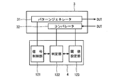
- the tester 3 includes a pattern generator 31 and a comparator 32.
- FIG. 2 is a schematic configuration diagram illustrating an example of the signal input / output circuit 33 that electrically connects the pattern generator 31 and the comparator 32 to the plurality of DUTs 10.
- the pattern generator 31 generates a test signal for inspecting the DUT 10.
- the pattern generator 31 and the plurality of DUTs 10 are connected by an input line 41 that is a wiring that branches into a plurality on the way.
- the comparator 32 In response to the test signal sent from the pattern generator 31, the comparator 32 outputs a response signal output from each of the plurality of DUTs 10 or a signal obtained by combining the response signals from the plurality of DUTs 10 (hereinafter referred to as “synthesis”).
- the response signal ” (which may be referred to as“ response signal ”) is compared with a threshold value.
- Connected to the comparator 32 is a common output line 51 that is a wiring for combining and transmitting response signals from the plurality of DUTs 10.
- the comparator 32 and the plurality of DUTs 10 are connected by a common output line 51 and an individual output line 52 that is a wiring from each DUT 10.
- the signal input / output circuit 33 includes an input line 41, a common output line 51, a plurality of individual output lines 52, a relay switch unit 53, and a resistance element 54.
- the signal input / output circuit 33 may be mounted on any of the tester 3, the support substrate 13 a of the probe card 13, or the interposer (or performance board) 22.
- the input line 41 branches along the way according to the number of DUTs 10 to be inspected at a time, and connects the pattern generator 31 and the plurality of DUTs 10 in parallel.
- the test signal generated by the pattern generator 31 is transmitted to a plurality of DUTs 10 via the input line 41.
- the input line 41 may be provided with a relay switch unit for switching connection / disconnection between the pattern generator 31 and the plurality of DUTs 10. Further, the input line 41 is not limited to the configuration shown in FIG. 2 as long as a test signal can be simultaneously transmitted to each DUT 10.
- the common output line 51 is formed by integrating a plurality of individual output lines 52 that transmit response signals output from the DUTs 10 based on the test signal input from the pattern generator 31.
- the response signal output from each DUT 10 is transmitted to the comparator 32 via the individual output line 52 and the common output line 51.
- each individual output line 52 a relay switch portion 53 and a resistance element 54 are provided in series.
- the arrangement order of the relay switch part 53 and the resistance element 54 is not ask
- the relay switch unit 53 can be used when switching connection / disconnection between the comparator 32 and the plurality of DUTs 10. When combining the response signals from the respective DUTs 10 into one, all the relay switch units 53 may be brought into a connected state (ON). When the response signal from each DUT 10 is individually sent to the comparator 32, only the relay switch unit 53 of one individual output line 52 is connected (ON), and the relay switch unit 53 of the other individual output line 52 is What is necessary is just to make it a non-connection state (OFF). In addition, when it is not necessary to send the response signal from each DUT 10 to the comparator 32 individually, the relay switch unit 53 may not be provided.
- the resistance element 54 has a function of selecting a response signal, and has a resistance larger than the internal resistance (output impedance) of each DUT 10 in order to adjust the impedance in the common output line 51 connected to each individual output line 52. Have.
- the control unit 4 is typically a computer.
- FIG. 3 shows an example of the hardware configuration of the control unit 4 shown in FIG.
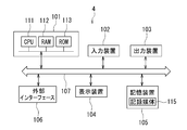
- the control unit 4 includes a main control unit 101, an input device 102 such as a keyboard and a mouse, an output device 103 such as a printer, a display device 104, a storage device 105, an external interface 106, and a bus that connects them together.
- the main control unit 101 includes a CPU (Central Processing Unit) 111, a RAM (Random Access Memory) 112, and a ROM (Read Only Memory) 113.
- CPU Central Processing Unit
- RAM Random Access Memory
- ROM Read Only Memory
- the storage device 105 is not particularly limited as long as it can store information, but is, for example, a hard disk device or an optical disk device.
- the storage device 105 records information on a computer-readable recording medium 115 and reads information from the recording medium 115.
- the recording medium 115 may be of any form as long as it can store information.
- the recording medium 115 is a hard disk, an optical disk, a flash memory, or the like.
- the recording medium 115 may be a recording medium that records a recipe for the inspection method according to the present embodiment.
- the CPU 111 uses the RAM 112 as a work area to execute a program stored in the ROM 113 or the storage device 105, so that the DUT 10 formed on the wafer W in the inspection apparatus 100 according to the present embodiment is processed.
- the inspection can be executed.
- the control unit 4 controls each component (for example, the mounting table 11, the alignment mechanism 14, the pattern generator 31, the comparator 32, the relay switch unit 53, etc.) in the inspection apparatus 100.
- FIG. 4 is a functional block diagram of the control unit 4 and also shows the relationship between the pattern generator 31 and the comparator 32 in the tester 3.
- the control unit 4 includes a signal control unit 121, a determination unit 122, and a threshold setting unit 123. These are realized by the CPU 111 executing software (programs) stored in the ROM 113 or the storage device 105 using the RAM 112 as a work area. For example, the same functions as those of the signal control unit 121, the determination unit 122, and the threshold setting unit 123 are performed using the FPGA (Field Programmable Gate Array) or the like, and the probe card 13 or the interposer (or performance board) 22 You may have it.
- the control part 4 also has other functions (for example, the control function etc. which switch connection / disconnection of the relay switch part 53), detailed description is abbreviate
- the signal control unit 121 controls the generation of the test signal by the pattern generator 31. Specifically, the signal control unit 121 sends a control signal to the pattern generator 31 to instruct the types of clock signals and data signals generated by the pattern generator 31, generation / stopping, and the like.
- the determination unit 122 acquires comparison information between the threshold value and the composite response signal from the comparator 32, and based on the comparison information, whether or not one or more of the plurality of DUTs 10 are rejected, that is, all It is determined whether or not the DUT 10 is acceptable. Note that this determination operation may be performed by the comparator 32 instead of the determination unit 122. Further, the determination unit 122 can determine the number of DUTs 10 that output the FAIL signal among the plurality of DUTs 10 based on a procedure described later.
- the threshold value setting unit 123 sets a threshold value for performing comparison in the comparator 32.
- the threshold value setting unit 123 can set a plurality of threshold values in multiple stages, and the threshold values can be dynamically changed. For example, when the determination unit 122 (or the comparator 32) determines that one or more of the plurality of DUTs 10 are unacceptable from the comparison information between the first threshold value and the synthesized response signal, the threshold value setting unit 123 can set the second threshold value as a new threshold value different from the first threshold value.
- FIG. 5 is an explanatory diagram of test signals, response signals, and threshold values in the conventional inspection method.
- the pattern generator 31 generates a clock signal (CLK) and a data signal (DATA), and these are input to each DUT 10 as a test signal.
- CLK clock signal
- DATA data signal
- PASS / FAIL pass / fail
- the individual response signal from each DUT 10 may include a PASS signal that satisfies the threshold value TH and a FAIL signal that does not satisfy the threshold value TH. Therefore, the synthesized response signal may be synthesized from only the PASS signal, synthesized from only the FAIL signal, or synthesized from the PASS signal and the FAIL signal.
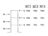
- FIG. 7 is a diagram for explaining an example of setting a threshold value for a composite response signal in the inspection method of the present embodiment.
- 6 and 7 exemplify the case where there are three DUTs 10.
- the signal level and signal pattern input from the pattern generator 31 have the same contents.
- the individual response signal from each DUT 10 may include a pass (PASS) and a fail (FAIL) as described above, and all cases are PASS and PASS and FAIL are mixed. Then, the synthesized response signals synthesized into one have different values.
- the output levels of the individual response signals of the DUT 10 are binary values of Hi (PASS): 3 [V] and Low (FAIL): 0 [V]
- the output level S D of two DUT10 individual response signals in the three DUT10 is Hi, when the output level S D of one DUT10 individual response signal is Low, FIG 6 (B ),
- the output impedance of the DUT 10 is the same at Hi: 3 [V] and Low: 0 [V].
- the output level of the composite response signal is sequentially compared with threshold values TH 1 , TH 2 , TH 3 .
- the determination unit 122 determines that “all DUTs 10 pass” if the output level of the composite response signal satisfies the threshold TH, and “one or more DUTs 10 fail if the threshold TH is not satisfied”. It is determined.
- the threshold TH 1 to be used is determined based on the combined response signal output level S 0 when all three DUTs 10 pass (PASS), and one DUT 10 fails. it may be set between the output level S 1 of the composite response signals when it is (FAIL). Accordingly, if the output level of the composite response signal is equal to or higher than the threshold TH 1 , all DUTs 10 pass (PASS), and if the output level is lower than the threshold TH 1 , one or more DUTs 10 fail (FAIL). It can be judged.
- the threshold TH 2 to be used is the output level S 1 of the composite response signal when one DUT 10 fails (FAIL) and the two DUTs 10 fail (FAIL) it may be set between the output level S 2 of the composite response signal. Accordingly, when the output level of the combined response signal is equal to or higher than the threshold TH 2 in combination with the first determination result, two DUTs 10 pass (PASS) and one DUT 10 fails (FAIL). I can judge. Further, if the output level is less than the threshold TH 2 of the composite response signals, two or more DUT10 can be judged to be a failure (FAIL).
- the threshold TH 3 to be used may be set to be less than the output level S 2 of the combined response signal when the two DUTs 10 fail (FAIL).
- FAIL the threshold level of the combined response signal
- the threshold TH 3 in combination with the first and second determination results, one DUT 10 is passed (PASS) and two DUTs 10 are rejected (FAIL). It can be judged that. Further, if the output level is less than the threshold value TH 3 Synthesis response signal, it can be determined that the three DUT10 is rejected (FAIL).
- the Nth (where N is a positive integer of 2 or more) DUTs 10 (where N is a positive integer of 1 or more)
- the threshold value set for the determination of THN is TH N
- the threshold value set for the N + 1th determination is TH N + 1
- the threshold TH N set for the Nth determination with respect to the output level S 0 of the composite response signal when all of the n DUTs 10 pass is expressed by the following equation (1). It is preferable to satisfy the relationship.
- the threshold value TH N is in the vicinity of an intermediate value between S 0 ⁇ [n ⁇ (N ⁇ 1)] / n and S 0 ⁇ (n ⁇ N) / n in order to increase the reliability of determination in consideration of the margin. It is more preferable to set to. That is, when the number of DUTs 10 that output the FAIL signal increases from zero by one, the combined response signals S 0 , S 1 , S 2 ,... S n are intermediate values between S 0 and S 1. It is preferable to set the threshold value TH N in the vicinity, near the intermediate value between S 1 and S 2 ,... Near the intermediate value between S n ⁇ 1 and S n . In this case, the threshold value TH N is preferably set to a value represented by the following equation (2), for example.
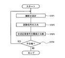
- FIG. 8 is a flowchart showing an example of the procedure of the inspection method according to the embodiment of the present invention.
- the inspection method of the present embodiment includes the processing of STEP1 to STEP4.
- a threshold value TH1 used in the first determination is set.
- This threshold TH 1 is set by the threshold setting unit 123. From the above formula (1), the threshold value TH 1 set in the first determination satisfies the following relationship with respect to the output level S 0 of the combined response signal when all of the n DUTs 10 pass. preferable.
- the margin TH 1 [S 0 ⁇ n / n + S 0 ⁇ (n ⁇ 1) / n] ⁇ 1/2 More preferably.
- the clock signal and the data signal are generated by the pattern generator 31 based on the command of the signal control unit 121, and the same test signal is input to all of the n DUTs 10 at the same time.
- the combined value (synthesized response signal) of the response signal output from each DUT 10 in response to the test signal is compared with the threshold value TH 1 by the comparator 32. In this case, all the relay switch parts 53 are maintained in a connection state (ON).
- the determination unit 122 obtains comparison information between the threshold value TH 1 and the composite response signal from the comparator 32, and one or more of the n DUTs 10 fail based on the comparison information. It is determined whether there is, that is, whether all the DUTs 10 pass.
- the process returns to STEP 1 again. That is, again in STEP 1, the threshold value setting unit 123 sets the threshold value TH 2 used in the second determination as a new threshold value. From the above equation (1), the threshold TH 2 set in the second determination satisfies the following relationship with respect to the output level S 0 of the combined response signal when all of the n DUTs 10 pass. preferable.
- a new threshold value for example, threshold value TH 2 used in the second determination
- the processing of STEP2 to STEP4 is executed, and the second determination is performed.
- the processing of STEP 1 to STEP 4 is repeatedly executed in a loop until it is determined in STEP 4 that “one or more of the n DUTs 10 are not rejected” (NO).
- NO the number of repetitions is set in advance, and when the upper limit is reached, a stop signal may be sent from the determination unit 122 to the signal control unit 121 and the threshold setting unit 123.
- the output levels S 0 , S 1 , S 2 ,... S N (where N Is a positive integer greater than or equal to 1), and by changing the threshold value TH, it is possible to determine the number of DUTs 10 that have output a FAIL signal among the n DUTs 10. That is, in the first determination, the threshold TH 1 is set to the output level S 0 of the combined response signal when all of the n DUTs 10 output the PASS signal (that is, the zero DUTs 10 output the FAIL signal). , One of the n DUTs 10 is set between the output level S 1 of the composite response signal when the FAIL signal is output (preferably in the vicinity of the intermediate value between the output level S 0 and the output level S 1 ). .
- the threshold value TH 2 is set such that the output level S 1 of the composite response signal when one of the n DUTs 10 outputs a FAIL signal, and two of the n DUTs 10 are It is set between the output level S 2 of the composite response signal when outputting the FAIL signal (preferably near the intermediate value between the output level S 1 and the output level S 2 ).
- the threshold value TH N is determined based on the output level S (N ⁇ 1) of the combined response signal when N ⁇ 1 of the n DUTs 10 output the FAIL signal, and the n DUTs 10.
- the control unit 4 is provided with a counter unit (not shown) connected to the threshold value setting unit 123, and each time the threshold value TH is set by the threshold value setting unit 123, one count is counted. It is also possible to increment. In this case, the count value (1, 2, 3,... N) counted by the counter unit is equal to the number of times the steps 1 to 4 are executed.
- the count value (1, 2, 3,... N) when it is finally determined in STEP 4 that “one or more of the n DUTs 10 are not rejected” (NO) is FAIL. Since the value is obtained by adding 1 to the number of DUTs 10 that output signals, the number of DUTs 10 that output FAIL signals can be quickly grasped.
- a step of correcting the threshold TH set by the threshold setting unit 123 based on these values may be provided.
- ⁇ Modification> In the inspection method of the present embodiment, as described above, the DUT 10 that has output the FAIL signal cannot be specified. Therefore, in addition to STEP 1 to STEP 4, a step of comparing the output level SD of the individual response signal from each DUT 10 with the threshold value TH may be provided. That is, when it is determined in STEP 4 that “one or more of the n DUTs 10 have failed” (YES), the process does not return to STEP 1 and the output level S D of the individual response signal from each DUT 10 is set as a threshold value. You may change so that it may compare with TH.
- the inspection method of the present embodiment since the comparison with the threshold value TH is performed using the synthesized response signal obtained by synthesizing the output signals from the plurality of DUTs 10, a failure (FAIL) is included in the plurality of DUTs 10. It is possible to quickly determine whether or not the DUT 10 that becomes) is included. Further, by repeatedly executing the steps STEP1 to STEP4 while changing the threshold value TH, it is possible to automatically determine the number of DUTs 10 that have output the FAIL signal among the n number of DUTs 10. Therefore, by using the inspection method of the present embodiment, efficient inspection can be performed in a short time in inspection of various semiconductor devices.
- FAIL failure
- the inspection method of this embodiment can be used for inspection of various semiconductor devices.
- it can be preferably used for a write test of a nonvolatile semiconductor memory element such as a NAND flash memory.
- the number of DUTs 10 that have output a FAIL signal can be determined automatically and quickly, but the DUT 10 that has output a FAIL signal cannot be identified.
- the pass / fail judgment for each DUT 10 and the identification of the defective DUT 10 can be confirmed by the read test.
- the embodiments of the present invention have been described in detail for the purpose of illustration, but the present invention is not limited to the above-described embodiments, and various modifications are possible.
- the inspection method of the present invention can be preferably used regardless of the type of device as long as the devices that output the READY signal / BUSY signal are inspected collectively.
Abstract
Description

図1は、本発明の一実施の形態に係る検査装置の概略構成を示す断面図である。図1において、検査装置100は、ローダー室1と、複数の検査対象デバイス(DUT)10(図1では図示せず)が形成されたウエハWを収容する検査室2と、ウエハW上のDUT10の電気的特性検査を行うテスタ3と、これら検査装置100の各構成部を制御する制御部4を備えている。
ローダー室1は、ウエハWを搬送する搬送領域を形成する。
検査室2は、ウエハWを載置する載置台11と、載置台11の上方に配置されたホルダ12と、を有している。載置台11は、ウエハWを載置した状態で、ウエハWをX、Y、Z及びθ方向に移動させることが可能に構成されている。ホルダ12は、プローブカード13を支持する。プローブカード13は、支持基板13aと複数のプローブ(接触子)13bとを有している。プローブカード13は、多数の接続端子を有する接続リング21及びインターポーザ(又はパフォーマンスボード)22、テストヘッド(図示省略)を介してテスタ3と電気的に接続されている。
テスタ3は、各DUT10に電気信号を送るとともに、DUT10からの応答信号を受信してウエハW上のDUT10の電気的特性検査を行う。テスタ3は、パターンジェネレータ31とコンパレータ32を備えている。
図2に示すように、信号入出力回路33は、入力ライン41と、共通出力ライン51と、複数の個別出力ライン52と、リレースイッチ部53と、抵抗素子54とを備えている。本実施の形態において、信号入出力回路33は、テスタ3、プローブカード13の支持基板13a、又は、インターポーザ(又はパフォーマンスボード)22のいずれかに実装されていればよい。
検査装置100の各構成部は、それぞれ制御部4に接続されて、制御部4によって制御される。制御部4は、典型的にはコンピュータである。図3は、図1に示した制御部4のハードウェア構成の一例を示している。制御部4は、主制御部101と、キーボード、マウス等の入力装置102と、プリンタ等の出力装置103と、表示装置104と、記憶装置105と、外部インターフェース106と、これらを互いに接続するバス107とを備えている。主制御部101は、CPU(中央処理装置)111、RAM(ランダムアクセスメモリ)112およびROM(リードオンリメモリ)113を有している。記憶装置105は、情報を記憶できるものであれば、その形態は問わないが、例えばハードディスク装置または光ディスク装置である。また、記憶装置105は、コンピュータ読み取り可能な記録媒体115に対して情報を記録し、また記録媒体115より情報を読み取るようになっている。記録媒体115は、情報を記憶できるものであれば、その形態は問わないが、例えばハードディスク、光ディスク、フラッシュメモリなどである。記録媒体115は、本実施の形態に係る検査方法のレシピを記録した記録媒体であってもよい。


次に、図8を参照しながら、検査装置100を用いて行われる本発明の一実施の形態に係る検査方法の具体的手順について説明する。図8は、本発明の一実施の形態に係る検査方法の手順の一例を示すフローチャートである。本実施の形態の検査方法は、STEP1~STEP4の処理を含む。
S0×n/n ≧ TH1 > S0×(n-1)/n
また、マージンを考慮して、
TH1=[S0×n/n+S0×(n-1)/n]×1/2
とすることがより好ましい。
S0×(n-1)/n ≧ TH2 > S0×(n-2)/n
また、マージンを考慮して、
TH2={[S0×(n-1)/n]+[S0×(n-2)/n]}×1/2
とすることがより好ましい。
すなわち、1回目の判定では、閾値TH1を、n個のDUT10のすべてがPASS信号を出力する(つまり、ゼロ個のDUT10がFAIL信号を出力する)場合の合成応答信号の出力レベルS0と、n個のDUT10の中の1個がFAIL信号を出力する場合の合成応答信号の出力レベルS1との間(好ましくは出力レベルS0と出力レベルS1との中間値付近)に設定する。
また、2回目の判定では、閾値TH2を、n個のDUT10の中の1個がFAIL信号を出力する場合の合成応答信号の出力レベルS1と、n個のDUT10の中の2個がFAIL信号を出力する場合の合成応答信号の出力レベルS2との間(好ましくは出力レベルS1と出力レベルS2との中間値付近)に設定する。
さらに、N回目の判定では、閾値THNを、n個のDUT10の中のN-1個がFAIL信号を出力する場合の合成応答信号の出力レベルS(N-1)と、n個のDUT10の中のN個がFAIL信号を出力する場合の合成応答信号の出力レベルSNとの間(好ましくは出力レベルS(N-1)と出力レベルSNとの中間値付近)に設定する。このように、閾値THを変更しながら、上記STEP1~STEP4の手順を繰り返し実行することにより、n個のDUT10の中で、FAIL信号を出力したDUT10の個数を自動的に判定することができる。
本実施の形態の検査方法では、上記のとおり、FAIL信号を出力したDUT10を特定することはできない。そのため、上記STEP1~STEP4に加え、各DUT10からの個別応答信号の出力レベルSDを閾値THと比較する工程を設けてもよい。すなわち、STEP4で「n個のDUT10のうち、1つ以上が不合格である」(YES)と判定された場合に、STEP1に戻らず、各DUT10からの個別応答信号の出力レベルSDを閾値THと比較するように変更してもよい。この場合、信号入出力回路33の一つの個別出力ライン52のリレースイッチ部53のみを接続状態(ON)、他の個別出力ライン52のリレースイッチ部53を非接続状態(OFF)にして個別応答信号をコンパレータ32へ送ればよい。なお、リレースイッチ部53を切り替える代わりに、複数のDUT10の中から任意のDUT10を選択して電気的に接続できるチップセレクト端子を利用してもよい。また、1回目の手順のSTEP4で「n個のDUT10のうち、1つ以上が不合格である」(YES)と判定された場合は、直ちに個別応答信号の判定に移行してもよいし、上記STEP1~STEP4の処理を所定回数(例えば5~10回)繰り返した後、それでもなおSTEP4で「n個のDUT10のうち、1つ以上が不合格である」(YES)と判定される場合にのみ、個別応答信号の判定に移行するようにしてもよい。
Claims (12)
- 基板上に形成された複数のデバイスの電気的特性を検査するデバイスの検査方法であって、
テスタに並列に接続された複数のデバイスに対して、前記テスタから同時に試験信号を入力する第1のステップと、
入力された前記試験信号に基づく前記複数のデバイスからの応答信号の合成値に基づき、前記複数のデバイスの1つ以上が不合格であるか否かの判定を行う第2のステップと、
を含むことを特徴とするデバイスの検査方法。 - 前記第2のステップでは、前記合成値を予め設定された閾値と比較し、前記閾値を充足しない場合は、前記複数のデバイスの1つ以上が不合格である、と判定するとともに、
前記第2のステップで前記閾値を充足しない場合に、前記閾値とは異なる新たな閾値を設定するステップをさらに備え、
前記新たな閾値を使用して、再度、前記第1のステップ及び前記第2のステップを行う請求項1に記載のデバイスの検査方法。 - 前記新たな閾値を設定するステップと、前記第1のステップと、前記第2のステップとを、前記新たな閾値を充足するまで繰り返し実行することによって、不合格である前記デバイスの数を検出する請求項2に記載のデバイスの検査方法。
- 前記閾値が、多段階に設定されており、N回目(ただし、Nは1以上の正の整数を意味する)の判定で設定される閾値をTHN、N+1回目の判定で設定される閾値をTHN+1とすると、THN>THN+1の関係を有するとともに、
前記複数のデバイスがn個(ただし、nは2以上の正の整数を意味する)のデバイスからなり、前記n個のデバイスの全てが合格である場合の前記応答信号の合成値がS0である場合に、前記閾値THNは、次の式(1)の関係を満たすものである請求項3に記載のデバイスの検査方法。

- 前記デバイスが、不揮発性半導体メモリであり、前記第1のステップ及び前記第2のステップが、前記不揮発性半導体メモリの書き込み試験として実行される請求項1に記載のデバイスの検査方法。
- 基板上に形成された複数のデバイスの電気的特性を検査するテスタと、前記基板との間に配置されるプローブカードであって、
複数の前記デバイスの電極パッドにそれぞれ接触させらせる複数のプローブと、
前記複数のプローブを支持する支持基板と、
を備え、
前記支持基板は、
前記プローブに接続され、前記テスタからの試験信号を複数の前記デバイスに伝送する入力ラインと、
前記プローブに接続され、前記試験信号に基づく前記デバイスからの応答信号を伝送する複数の個別出力ラインと、
複数の前記個別出力ラインを統合し、複数の前記デバイスからの前記応答信号を合成して前記テスタへ向けて伝送する共通出力ラインと、
を有し、
前記個別出力ラインに、前記デバイスの内部抵抗よりも大きな抵抗を有する抵抗部を備えていることを特徴とするプローブカード。 - 前記個別出力ラインに、さらに、前記抵抗部と直列に接続されたリレースイッチ部を有している請求項6に記載のプローブカード。
- 基板上に形成された複数のデバイスの電気的特性を検査するテスタと、前記基板との間に配置されるインターポーザであって、
前記テスタからの試験信号を、複数の前記デバイスに向けて伝送する入力ラインと、
前記試験信号に基づく前記デバイスからの応答信号を伝送する複数の個別出力ラインと、
複数の前記個別出力ラインを統合し、複数の前記デバイスからの前記応答信号を合成して前記テスタへ向けて伝送する共通出力ラインと、
を有し、
前記個別出力ラインに、前記デバイスの内部抵抗よりも大きな抵抗を有する抵抗部を備えていることを特徴とするインターポーザ。 - 前記個別出力ラインに、さらに、前記抵抗部と直列に接続されたリレースイッチ部を有している請求項8に記載のインターポーザ。
- 基板上に形成された複数のデバイスの電気的特性を検査する検査装置であって、
前記デバイスを検査するための試験信号を生成するパターンジェネレータと、
前記試験信号に基づく複数の前記デバイスからの応答信号を合成した合成応答信号を閾値と比較するコンパレータと、
前記パターンジェネレータ及びコンパレータと、前記デバイスとの間に介在する信号入出力回路と、
を備え、
前記信号入出力回路は、
前記試験信号を、複数の前記デバイスに向けて伝送する入力ラインと、
前記試験信号に基づく前記デバイスからの応答信号を伝送する複数の個別出力ラインと、
複数の前記個別出力ラインを統合し、複数の前記デバイスからの前記応答信号を合成して前記コンパレータへ向けて伝送する共通出力ラインと、
を有し、前記個別出力ラインに、前記デバイスの内部抵抗よりも大きな抵抗を有する抵抗部を備えていることを特徴とする検査装置。 - 前記個別出力ラインに、さらに、前記抵抗部と直列に接続されたリレースイッチ部を有している請求項10に記載の検査装置。
- 前記パターンジェネレータによる前記試験信号の生成を制御する信号制御部と、
前記コンパレータによる、前記閾値と前記合成応答信号との比較情報に基づき、複数の前記デバイスのうち、1つ以上が不合格であるか否かを判定する判定部と、
前記判定部によって、前記複数のデバイスのうち、1つ以上が不合格である、と判定された場合に、前記閾値とは異なる新たな閾値を設定する閾値設定部と、
を有する制御部を、さらに備えた請求項10に記載の検査装置。
Priority Applications (4)
| Application Number | Priority Date | Filing Date | Title |
|---|---|---|---|
| SG11201700713QA SG11201700713QA (en) | 2014-08-01 | 2015-06-10 | Device inspection method, probe card, interposer, and inspection apparatus |
| CN201580040295.8A CN106662613A (zh) | 2014-08-01 | 2015-06-10 | 器件的检查方法、探针卡、中继板以及检查装置 |
| US15/501,151 US20170256324A1 (en) | 2014-08-01 | 2015-06-10 | Device inspection method, probe card, interposer, and inspection apparatus |
| KR1020177005706A KR20170038050A (ko) | 2014-08-01 | 2015-06-10 | 디바이스의 검사 방법, 프로브 카드, 인터포저 및 검사 장치 |
Applications Claiming Priority (2)
| Application Number | Priority Date | Filing Date | Title |
|---|---|---|---|
| JP2014157753A JP2016035957A (ja) | 2014-08-01 | 2014-08-01 | デバイスの検査方法、プローブカード、インターポーザ及び検査装置 |
| JP2014-157753 | 2014-08-01 |
Publications (1)
| Publication Number | Publication Date |
|---|---|
| WO2016017292A1 true WO2016017292A1 (ja) | 2016-02-04 |
Family
ID=55217197
Family Applications (1)
| Application Number | Title | Priority Date | Filing Date |
|---|---|---|---|
| PCT/JP2015/066660 WO2016017292A1 (ja) | 2014-08-01 | 2015-06-10 | デバイスの検査方法、プローブカード、インターポーザ及び検査装置 |
Country Status (7)
| Country | Link |
|---|---|
| US (1) | US20170256324A1 (ja) |
| JP (1) | JP2016035957A (ja) |
| KR (1) | KR20170038050A (ja) |
| CN (1) | CN106662613A (ja) |
| SG (1) | SG11201700713QA (ja) |
| TW (1) | TWI660183B (ja) |
| WO (1) | WO2016017292A1 (ja) |
Cited By (1)
| Publication number | Priority date | Publication date | Assignee | Title |
|---|---|---|---|---|
| JP2021527203A (ja) * | 2018-06-08 | 2021-10-11 | テラダイン、 インコーポレイテッド | 分散されたリソースを有する試験システム |
Families Citing this family (8)
| Publication number | Priority date | Publication date | Assignee | Title |
|---|---|---|---|---|
| JP6738236B2 (ja) * | 2016-08-12 | 2020-08-12 | 東京エレクトロン株式会社 | デバイス検査回路、デバイス検査装置及びプローブカード |
| US10333260B2 (en) * | 2016-08-31 | 2019-06-25 | Semiconductor Components Industries, Llc | High contact resistance detection |
| JP2018194356A (ja) | 2017-05-15 | 2018-12-06 | 東京エレクトロン株式会社 | デバイスの検査方法 |
| KR102577446B1 (ko) * | 2019-02-12 | 2023-09-11 | 삼성전자주식회사 | 테스트 보드 및 이의 제조 방법, 테스트 보드를 이용한 소자 검사 장비, 및 테스트 보드를 이용한 반도체 장치의 제조 방법 |
| US11899550B2 (en) * | 2020-03-31 | 2024-02-13 | Advantest Corporation | Enhanced auxiliary memory mapped interface test systems and methods |
| KR20210147319A (ko) | 2020-05-28 | 2021-12-07 | 삼성전자주식회사 | 번 인 보드 테스트 장치 및 시스템 |
| US11486926B1 (en) * | 2020-12-04 | 2022-11-01 | Xilinx, Inc. | Wearout card use count |
| FR3130066A1 (fr) * | 2021-12-07 | 2023-06-09 | Hprobe | Dispositif et procédé de test de mémoire |
Citations (3)
| Publication number | Priority date | Publication date | Assignee | Title |
|---|---|---|---|---|
| JP2000346910A (ja) * | 1999-06-07 | 2000-12-15 | Yamada Denon Kk | Icの多数並列同時テスト用測定装置 |
| WO2008044391A1 (fr) * | 2006-10-05 | 2008-04-17 | Advantest Corporation | Dispositif de contrôle, procédé de contrôle et procédé de fabrication |
| JP2011053180A (ja) * | 2009-09-04 | 2011-03-17 | Fujitsu Ltd | 半導体試験回路、半導体試験用冶具、半導体試験装置及び半導体試験方法 |
Family Cites Families (6)
| Publication number | Priority date | Publication date | Assignee | Title |
|---|---|---|---|---|
| JPH0743426B2 (ja) * | 1989-12-20 | 1995-05-15 | 三菱電機株式会社 | 超音波障害物センサ |
| CA2174784C (en) * | 1996-04-23 | 1999-07-13 | George Guozhen Zhong | Automatic multi-probe pwb tester |
| JPH11311661A (ja) * | 1998-04-30 | 1999-11-09 | Nec Corp | 半導体装置試験システムおよび半導体装置試験方法 |
| US6798225B2 (en) * | 2002-05-08 | 2004-09-28 | Formfactor, Inc. | Tester channel to multiple IC terminals |
| DE10306620B4 (de) * | 2003-02-18 | 2007-04-19 | Infineon Technologies Ag | Integrierte Testschaltung in einer integrierten Schaltung |
| JP3767829B1 (ja) * | 2005-06-09 | 2006-04-19 | エスティケイテクノロジー株式会社 | 半導体デバイスの検査装置 |
-
2014
- 2014-08-01 JP JP2014157753A patent/JP2016035957A/ja active Pending
-
2015
- 2015-06-10 KR KR1020177005706A patent/KR20170038050A/ko not_active Application Discontinuation
- 2015-06-10 CN CN201580040295.8A patent/CN106662613A/zh active Pending
- 2015-06-10 US US15/501,151 patent/US20170256324A1/en not_active Abandoned
- 2015-06-10 SG SG11201700713QA patent/SG11201700713QA/en unknown
- 2015-06-10 WO PCT/JP2015/066660 patent/WO2016017292A1/ja active Application Filing
- 2015-07-23 TW TW104123874A patent/TWI660183B/zh active
Patent Citations (3)
| Publication number | Priority date | Publication date | Assignee | Title |
|---|---|---|---|---|
| JP2000346910A (ja) * | 1999-06-07 | 2000-12-15 | Yamada Denon Kk | Icの多数並列同時テスト用測定装置 |
| WO2008044391A1 (fr) * | 2006-10-05 | 2008-04-17 | Advantest Corporation | Dispositif de contrôle, procédé de contrôle et procédé de fabrication |
| JP2011053180A (ja) * | 2009-09-04 | 2011-03-17 | Fujitsu Ltd | 半導体試験回路、半導体試験用冶具、半導体試験装置及び半導体試験方法 |
Cited By (2)
| Publication number | Priority date | Publication date | Assignee | Title |
|---|---|---|---|---|
| JP2021527203A (ja) * | 2018-06-08 | 2021-10-11 | テラダイン、 インコーポレイテッド | 分散されたリソースを有する試験システム |
| JP7288464B2 (ja) | 2018-06-08 | 2023-06-07 | テラダイン、 インコーポレイテッド | 分散されたリソースを有する試験システム |
Also Published As
| Publication number | Publication date |
|---|---|
| US20170256324A1 (en) | 2017-09-07 |
| TWI660183B (zh) | 2019-05-21 |
| TW201617633A (zh) | 2016-05-16 |
| SG11201700713QA (en) | 2017-03-30 |
| JP2016035957A (ja) | 2016-03-17 |
| KR20170038050A (ko) | 2017-04-05 |
| CN106662613A (zh) | 2017-05-10 |
Similar Documents
| Publication | Publication Date | Title |
|---|---|---|
| WO2016017292A1 (ja) | デバイスの検査方法、プローブカード、インターポーザ及び検査装置 | |
| KR20100105499A (ko) | 집적 회로 병렬 테스트 방법, 장치 및 시스템 | |
| US8466702B2 (en) | Test system and substrate unit for testing | |
| CN108572310B (zh) | 电路测试方法 | |
| US11644503B2 (en) | TSV testing using test circuits and grounding means | |
| US20200174073A1 (en) | Device inspection method | |
| US10048306B1 (en) | Methods and apparatus for automated integrated circuit package testing | |
| JP2010133817A (ja) | 絶縁検査装置および絶縁検査方法 | |
| KR101781895B1 (ko) | 멀티칩 패키지 테스트 시스템 | |
| US20150168482A1 (en) | Configurable test equipment | |
| JP5663943B2 (ja) | 試験装置 | |
| KR100977060B1 (ko) | 반도체칩 테스터용 프로브 카드와 이를 사용하는 테스터 및그 테스터를 이용한 반도체칩의 검사방법 | |
| KR20090043356A (ko) | Usb 플래시메모리용 실장 검사 장치 | |
| TW202013544A (zh) | 晶圓級測試方法及系統 | |
| JP2010165819A (ja) | 半導体集積回路の試験装置、試験方法 | |
| JP2012083262A (ja) | 試験装置および試験方法 | |
| KR100902269B1 (ko) | 반도체 테스트 장치 및 이를 이용한 반도체 소자 테스트방법 | |
| JP2007012709A (ja) | 半導体検査装置および半導体装置の検査方法 | |
| JP4137082B2 (ja) | 半導体装置の試験装置 | |
| JP6798834B2 (ja) | 検査装置、検査システム、検査方法、及び検査プログラム | |
| KR20060005820A (ko) | 반도체 소자의 병렬 테스트용 장치 및 병렬 테스트 방법 | |
| TW202339160A (zh) | 半導體裝置及半導體裝置的測試方法 | |
| KR100916763B1 (ko) | 반도체 디바이스 테스트 시스템 | |
| KR100921222B1 (ko) | 반도체 테스트 헤드 장치 | |
| JP2005274516A (ja) | 半導体集積回路及びその試験手法 |
Legal Events
| Date | Code | Title | Description |
|---|---|---|---|
| 121 | Ep: the epo has been informed by wipo that ep was designated in this application |
Ref document number: 15828296 Country of ref document: EP Kind code of ref document: A1 |
|
| NENP | Non-entry into the national phase |
Ref country code: DE |
|
| WWE | Wipo information: entry into national phase |
Ref document number: 15501151 Country of ref document: US |
|
| ENP | Entry into the national phase |
Ref document number: 20177005706 Country of ref document: KR Kind code of ref document: A |
|
| 122 | Ep: pct application non-entry in european phase |
Ref document number: 15828296 Country of ref document: EP Kind code of ref document: A1 |