WO2016013418A1 - 被処理体を処理する方法 - Google Patents
被処理体を処理する方法 Download PDFInfo
- Publication number
- WO2016013418A1 WO2016013418A1 PCT/JP2015/069861 JP2015069861W WO2016013418A1 WO 2016013418 A1 WO2016013418 A1 WO 2016013418A1 JP 2015069861 W JP2015069861 W JP 2015069861W WO 2016013418 A1 WO2016013418 A1 WO 2016013418A1
- Authority
- WO
- WIPO (PCT)
- Prior art keywords
- gas
- plasma
- processing
- magnetic layer
- processing gas
- Prior art date
- Legal status (The legal status is an assumption and is not a legal conclusion. Google has not performed a legal analysis and makes no representation as to the accuracy of the status listed.)
- Ceased
Links
Images




Classifications
-
- H—ELECTRICITY
- H10—SEMICONDUCTOR DEVICES; ELECTRIC SOLID-STATE DEVICES NOT OTHERWISE PROVIDED FOR
- H10P—GENERIC PROCESSES OR APPARATUS FOR THE MANUFACTURE OR TREATMENT OF DEVICES COVERED BY CLASS H10
- H10P50/00—Etching of wafers, substrates or parts of devices
- H10P50/20—Dry etching; Plasma etching; Reactive-ion etching
- H10P50/24—Dry etching; Plasma etching; Reactive-ion etching of semiconductor materials
- H10P50/242—Dry etching; Plasma etching; Reactive-ion etching of semiconductor materials of Group IV materials
-
- H—ELECTRICITY
- H10—SEMICONDUCTOR DEVICES; ELECTRIC SOLID-STATE DEVICES NOT OTHERWISE PROVIDED FOR
- H10B—ELECTRONIC MEMORY DEVICES
- H10B61/00—Magnetic memory devices, e.g. magnetoresistive RAM [MRAM] devices
-
- H—ELECTRICITY
- H10—SEMICONDUCTOR DEVICES; ELECTRIC SOLID-STATE DEVICES NOT OTHERWISE PROVIDED FOR
- H10N—ELECTRIC SOLID-STATE DEVICES NOT OTHERWISE PROVIDED FOR
- H10N50/00—Galvanomagnetic devices
- H10N50/01—Manufacture or treatment
-
- H—ELECTRICITY
- H10—SEMICONDUCTOR DEVICES; ELECTRIC SOLID-STATE DEVICES NOT OTHERWISE PROVIDED FOR
- H10N—ELECTRIC SOLID-STATE DEVICES NOT OTHERWISE PROVIDED FOR
- H10N50/00—Galvanomagnetic devices
- H10N50/10—Magnetoresistive devices
-
- H—ELECTRICITY
- H10—SEMICONDUCTOR DEVICES; ELECTRIC SOLID-STATE DEVICES NOT OTHERWISE PROVIDED FOR
- H10N—ELECTRIC SOLID-STATE DEVICES NOT OTHERWISE PROVIDED FOR
- H10N50/00—Galvanomagnetic devices
- H10N50/80—Constructional details
- H10N50/85—Materials of the active region
-
- H—ELECTRICITY
- H10—SEMICONDUCTOR DEVICES; ELECTRIC SOLID-STATE DEVICES NOT OTHERWISE PROVIDED FOR
- H10P—GENERIC PROCESSES OR APPARATUS FOR THE MANUFACTURE OR TREATMENT OF DEVICES COVERED BY CLASS H10
- H10P14/00—Formation of materials, e.g. in the shape of layers or pillars
- H10P14/60—Formation of materials, e.g. in the shape of layers or pillars of insulating materials
- H10P14/65—Formation of materials, e.g. in the shape of layers or pillars of insulating materials characterised by treatments performed before or after the formation of the materials
- H10P14/6502—Formation of materials, e.g. in the shape of layers or pillars of insulating materials characterised by treatments performed before or after the formation of the materials of treatments performed before formation of the materials
- H10P14/6512—Formation of materials, e.g. in the shape of layers or pillars of insulating materials characterised by treatments performed before or after the formation of the materials of treatments performed before formation of the materials by exposure to a gas or vapour
- H10P14/6514—Formation of materials, e.g. in the shape of layers or pillars of insulating materials characterised by treatments performed before or after the formation of the materials of treatments performed before formation of the materials by exposure to a gas or vapour by exposure to a plasma
Definitions
- Embodiment of this invention is related with the method of processing a to-be-processed object.
- a magnetic random access memory (MRAM) element is a memory having a magnetic tunnel junction (MTJ), and has two magnetic layers and an insulating layer provided between the magnetic layers. is doing.
- the magnetic layer is made of a metal such as Co and / or Fe.
- etching for transferring the mask pattern to the two magnetic layers and the insulating film of the object to be processed is performed.
- a reaction product that is difficult to vaporize is generated, and the reaction product is deposited on the object to be processed.
- This reaction product can cause various problems such as leakage current of the MRAM device and needs to be removed.
- Patent Document 1 describes a method for removing a reaction product.
- the upper magnetic layer of the two magnetic layers that is, the lower magnetic layer and the upper magnetic layer
- a processing gas containing a halogen element is etched by plasma of a processing gas containing a halogen element.
- a protective film is formed on the surface of the object to be processed.
- the insulating layer is then etched.
- the reaction product is removed by a processing gas containing PF 3 gas.
- reaction products that is, deposits are also formed on the object to be processed by etching the upper magnetic layer.
- the method described in Patent Document 1 only removes the reaction product formed by etching the insulating layer, and does not remove the deposit formed by etching the upper magnetic layer. .
- the deposit formed by etching the upper magnetic layer also needs to be removed.
- a method for treating a workpiece includes a lower magnetic layer, an insulating layer provided on the lower magnetic layer, an upper magnetic layer provided on the insulating layer, and a mask provided on the upper magnetic layer.
- This method is a step of (a) etching the upper magnetic layer, supplying a first processing gas into a processing container of a plasma processing apparatus, generating plasma of the first processing gas, and generating the first processing gas. Etching the upper magnetic layer with the plasma of the process gas (hereinafter referred to as “process a”), and (b) removing the deposit formed on the object to be processed by the process a (hereinafter referred to as “process a”). Step b)).
- Step b includes (b1) a step of causing a reduction reaction to occur in the deposit by the plasma of the second processing gas containing H 2 gas, and (b2) a product generated by the step of causing the reduction reaction to be converted to hexa Removing with a third process gas containing fluoroacetylacetone.
- the top magnetic layer can include CoFeB.
- the deposit formed by etching the upper magnetic layer in step a may contain a metal oxide.
- This metal oxide is formed by the reaction between the metal contained in the upper magnetic layer and oxygen. Oxygen is considered to be generated from a layer included in the object to be processed or various parts of the plasma processing apparatus.
- a reduction reaction is caused in the deposit by the plasma of the second processing gas containing H 2 gas.
- the product obtained from the deposit by this reduction reaction can be removed by the third processing gas containing hexafluoroacetylacetone. Therefore, according to this method, it is possible to remove deposits formed by etching the upper magnetic layer.
- step a and step b may be repeated alternately. According to this embodiment, by repeating step a and step b, it is possible to prevent the generation of a large amount of deposits and remove the deposits generated by the etching in step a.
- the second process gas may further include N 2 gas.
- the second processing gas contains N 2 gas, the plasma of the second processing gas can be generated stably.
- the third process gas may include H 2 O. According to this embodiment, it is possible to promote the reaction between the product obtained by the reduction reaction and hexafluoroacetylacetone.
- the method of an embodiment may further include the step of etching the insulating layer.
- a fourth processing gas is supplied into a processing container of the plasma processing apparatus, plasma of the fourth processing gas is generated, and the insulating layer is formed by the plasma of the fourth processing gas. Etch.
- FIG. 6 is a flowchart showing details of the process ST5 shown in FIG. FIG.
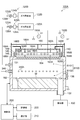
- FIG. 2 schematically illustrates a processing system of an embodiment that can be used to implement the method shown in FIG. 1. It is a figure which shows schematically the plasma processing apparatus which can be used as process module PM1 shown in FIG. It is a figure which shows roughly the plasma processing apparatus which can be used as process module PM2 shown in FIG. It is a figure which shows roughly the plasma processing apparatus which can be used as process module PM4 shown in FIG.
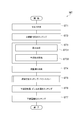
- FIG. 1 is a flowchart of a method for processing an object to be processed according to an embodiment.
- a method MT shown in FIG. 1 is a method used in the manufacture of a magnetic random access memory (MRAM) element. At least a step ST2 for etching the upper magnetic layer and a step ST3 for removing deposits. Is included.
- the method MT includes steps ST1 and ST4 to ST7 in addition to the steps ST2 and ST3.
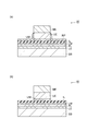
- FIG. 2 is a cross-sectional view showing an example of an object to be processed to which the method shown in FIG. 1 is applied, and a state of the object to be processed after each process of the method shown in FIG.
- an object to be processed to which the method MT is applied includes a substrate SB, a lower electrode layer LE, a pinning layer PL, a lower magnetic layer LM, an insulating layer.
- the layer IL, the upper magnetic layer UM, the upper electrode layer UE, and the mask layer ML are included.
- the lower electrode layer LE is a layer made of an electrode material having electrical conductivity, and is provided on the substrate SB.
- the thickness of the lower electrode layer LE is, for example, about 5 nm.
- the pinning layer PL is provided between the lower electrode layer LE and the lower magnetic layer LM.
- the pinning layer PL in the MRAM element functions as a layer for fixing the magnetization direction of the lower magnetic layer LM due to the pinning effect by the antiferromagnetic material.
- the pinning layer PL is made of, for example, an antiferromagnetic material such as IrMn (iridium manganese) or PtMn (platinum manganese), and has a thickness of about 7 nm, for example.
- the lower magnetic layer LM is a layer containing a ferromagnetic material and is provided on the pinning layer PL.
- the lower magnetic layer LM is a layer that functions as a so-called pinned layer. That is, in the MRAM element, the magnetization direction of the lower magnetic layer LM is kept constant without being influenced by the external magnetic field due to the pinning effect by the pinning layer PL.
- the lower magnetic layer LM is made of, for example, CoFeB and has a thickness of, for example, about 2.5 nm.
- the insulating layer IL is provided between the lower magnetic layer LM and the upper magnetic layer UM.
- the insulating layer IL in the MRAM element constitutes a magnetic tunnel junction (MTJ).
- MTJ magnetic tunnel junction
- the insulating layer IL is interposed between the lower magnetic layer LM and the upper magnetic layer UM, so that the tunnel magnetoresistance is between the lower magnetic layer LM and the upper magnetic layer UM.
- An effect (TMR: Tunnel magnetoresistance) occurs. That is, an electrical resistance is generated between the lower magnetic layer LM and the upper magnetic layer UM according to the relative relationship (parallel or antiparallel) between the magnetization direction of the lower magnetic layer LM and the magnetization direction of the upper magnetic layer UM.
- This insulating layer IL is made of Al 2 O 3 or MgO, and its thickness is, for example, 1.3 nm.
- the upper magnetic layer UM is a layer containing a ferromagnetic material, and is provided on the insulating layer IL.
- the upper magnetic layer UM in the MRAM element is a layer that functions as a so-called free layer. That is, in the MRAM element, the magnetization direction of the upper magnetic layer UM follows an external magnetic field that is magnetic information.
- the upper magnetic layer UM is made of, for example, CoFeB and has a thickness of, for example, about 2.5 nm.
- the upper electrode layer UE is a layer composed of an electrode material having electrical conductivity.
- the upper electrode layer UE can be made of Ta, for example.
- the mask layer ML is a layer serving as a mask for etching the upper electrode layer UE and the upper magnetic layer UM.
- the mask layer ML can be composed of, for example, a first layer containing amorphous carbon and a second layer containing SiO 2 .
- the second layer is provided on the upper electrode layer UE, and the first layer is provided on the second layer.
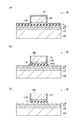
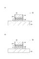
- FIGS. 3 to 5 are cross-sectional views showing the state of the object to be processed after each step of the method shown in FIG.
- the process ST1 is performed.
- step ST1 as shown in FIG. 2B, a mask MK is created from the mask layer ML.
- the mask MK can be formed by providing a patterned mask on the first layer and sequentially etching the first layer and the second layer of the mask layer ML.
- the first layer can be etched by plasma of a processing gas containing O 2 gas
- the second layer can be etched by plasma of a processing gas containing fluorocarbon gas.
- the upper magnetic layer UM is etched.
- the upper electrode layer UE and the upper magnetic layer UM are etched together.
- the processing gas A (first processing gas) is supplied into the processing container of the plasma processing apparatus.
- the processing gas A can contain a halogen element. Further, the processing gas A may further contain a rare gas.
- the processing gas A includes SF 6 gas and Ar gas.
- plasma of the processing gas A is generated.
- the wafer W is exposed to the plasma of the processing gas A.
- the upper electrode layer UE and the upper magnetic layer UM are etched, and the pattern of the mask MK is transferred to the upper electrode layer UE and the upper magnetic layer UM.
- a deposit DP is formed on the wafer W as shown in FIG. Specifically, the deposit DP is formed on the side surface of the upper electrode layer UE, the side surface of the upper magnetic layer UM, and the surface of the insulating layer IL.
- the deposit DP includes Co and Fe oxides included in the upper magnetic layer UM. It is considered that the oxides of Co and Fe in the deposit DP are derived from oxidation of Co and Fe by SiO 2 contained in the mask MK or oxygen generated from various parts of the plasma processing apparatus.
- step ST3 includes a step ST31 and a step ST32.
- step ST31 a process for causing a reduction reaction on the deposit is performed.
- a processing gas B second processing gas
- H 2 gas is supplied into the processing container of the plasma processing apparatus.
- plasma of the processing gas B is generated.
- step ST31 the wafer W is exposed to the plasma of the processing gas B.
- the reduction reaction of deposit DP arises and the product RP is produced
- oxygen is removed from Co and Fe oxides in the deposit DP, and a product RP containing Co and Fe is obtained.
- the processing gas used in step ST31 may include N 2 gas in addition to H 2 gas.
- the plasma of the second processing gas can be generated stably.
- the processing gas C (third processing gas) containing hexafluoroacetylacetone is supplied into the processing container containing the wafer W.
- hexafluoroacetylacetone is 1,1,1,5,5,5-hexafluoroacetylacetone (hereinafter referred to as “hfacH”).
- the process gas C may include H 2 O and / or O 2 gas.
- Co and Fe contained in the product RP are complexed by hfac.
- Hfac is a hexafluoroacetylacetonate ligand that is generated when hydrogen (H) is released from hfacH and the hfacH becomes a monovalent anion.
- a Co complex is formed from Co in the product RP. Co + 2 (hfac) + 2H 2 O ⁇ Co (H 2 O) 2 (hfac) 2
- step ST32 the complex thus generated is removed.
- the product RP is removed as shown in FIG.
- H 2 O is contained in the processing gas C
- H 2 O is added to the processing gas C for the purpose of promoting the reaction of the above reaction formula and facilitating the formation of a complex of Co and hafc.
- the process ST31 and the process ST32 may be alternately repeated.
- the upper magnetic layer UM is partially etched in the process ST31, and a relatively small amount of deposit DP generated by the process ST31 is removed in the process ST32.
- the steps ST31 and ST32 it is possible to prevent the generation of a large amount of deposit DP and to remove the deposit DP generated by the etching in the step ST31.
- step ST4 is performed.
- the wafer W is transferred to the film forming apparatus.
- a protective film PF is formed on the surface of the wafer W.
- This protective film PF is made of, for example, SiN or SiO 2 .
- the mask MK is omitted. The mask MK may disappear during the execution of the process after the process ST4, or may be removed before the execution of the process ST4.
- step ST5 is performed.
- FIG. 6 is a flowchart showing details of the process ST5 shown in FIG.
- the process ST5 includes a process ST51 and a process ST52.
- the processing gas D fourth processing gas
- the processing gas D is supplied into the processing container of the plasma processing apparatus, and plasma of the processing gas D is generated.
- the insulating layer IL is etched in a region not covered by the upper electrode layer UE, the upper magnetic layer UM, and the protective film PF.
- the processing gas D used in the process ST51 is a decomposable gas that is dissociated by plasma generated by a plasma source and generates radicals.
- This radical may be a radical that causes a reduction reaction, an oxidation reaction, a chlorination reaction, or a fluorination reaction.
- the processing gas D may be a gas containing a hydrogen element, an oxygen element, a chlorine element, or a fluorine element.
- the processing gas D may include Ar, N 2 , O 2 , H 2 , He, BCl 3 , Cl 2 , CF 4 , NF 3 , CH 4, SF 6, or the like.
- the processing gas D may contain O 2 gas, Ar gas, H 2 gas, Cl 2 gas, and NF 3 gas.
- the reaction product RP2 includes a metal contained in the upper electrode layer UE, the protective film PF, and the insulating layer IL, an oxide, chloride, nitride, halide, or a compound containing C or Si, or the like of the metal. May be included.
- the reaction product RP2 adheres to the side surface of the shape formed by etching and / or the surface of the lower magnetic layer LM.
- the reaction product RP2 formed in this way reduces the verticality of the shape formed by subsequent etching.
- the reaction product RP2 contains a conductive substance, if the reaction product RP2 is left, it may be a factor that causes a leakage current to the MRAM element.
- step ST52 a treatment process using an etching gas containing PF 3 is performed.
- the processing gas E is supplied into the processing container of the same plasma processing apparatus as in step ST51.
- This processing gas E is a reactive gas for reacting with a reaction product without being exposed to plasma.
- the processing gas E may include, for example, a gas whose reaction with the reaction product depends on the temperature of the mounting table 110. Specifically, HF, Cl 2 , HCl, H 2 O, PF 3 , F 2 , ClF 3 , COF 2 , cyclopentadiene, Amidinato, or the like is used as the processing gas E.
- the processing gas E may include an electron donating gas.
- the electron donating gas is generally a gas composed of atoms having greatly different electronegativity or ionization potential, or a gas including atoms having a lone electron pair.
- the electron donating gas has a property of easily giving electrons to other compounds.
- the electron donating gas has a property of being bonded to a metal compound or the like as a ligand and evaporating.
- the electron donating gas examples include SF 6 , PH 3 , PF 3 , PCl 3 , PBr 3 , PI 3 , CF 4 , AsH 3 , SbH 3 , SO 3 , SO 2 , H 2 S, SeH 2 , TeH 2 , Examples thereof include Cl 3 F, H 2 O, H 2 O 2 and the like, or a gas containing a carbonyl group.
- the processing gas E may include PF 3 gas.
- processing gas used in either or both of the steps ST51 and step ST52 may include PF 3 gas.
- process ST51 and process ST52 may be repeated alternately.
- the lower magnetic layer LM and the pinning layer PL are etched.
- a processing gas containing CH 4 is supplied into the processing container of the plasma processing apparatus.
- the processing gas F may include an inert gas such as He, N 2 , Ar, and / or a gas other than methane, such as a gas containing a carbonyl group, H 2, or the like.
- plasma of the processing gas F is generated, and the wafer W is exposed to the plasma.
- FIG. 5A the lower magnetic layer LM and the pinning layer PL are etched in a region not covered with the upper electrode layer UE, the upper magnetic layer UM, and the protective film PF.
- the lower electrode layer LE is etched.
- the processing gas G is supplied into the processing container of the plasma processing apparatus.
- the processing gas G may include an inert gas such as He, N 2 , Ar, and / or a gas containing a carbonyl group, CH 4, H 2, or the like.
- plasma of the processing gas G is generated, and the wafer W is exposed to the plasma.
- FIG. 5B the lower electrode layer LE is etched in a region not covered with the upper electrode layer UE and the upper magnetic layer UM, and an MRAM element is formed.
- a reduction reaction is caused in the deposit DP by the plasma of the processing gas B containing H 2 gas.
- the product RP obtained from the deposit DP by this reduction reaction can be removed by the processing gas C containing hexafluoroacetylacetone. Therefore, according to this method, as shown in FIG. 3B, the deposit DP formed by etching the upper magnetic layer UM can be removed. If the processing gas used in step ST31 does not contain H 2 gas, the reduction reaction does not occur. Therefore, even if the wafer is exposed to the processing gas C in step ST32, the state changes from the state shown in FIG. Does not substantially occur and the deposit DP is not removed.
- FIG. 7 schematically illustrates a processing system of one embodiment that can be used to implement the method illustrated in FIG.
- the processing system PS shown in FIG. 7 includes substrate mounting tables 22a to 22d, receiving containers 24a to 24d, a loader module LDM, a load lock chamber LL1, a load lock chamber LL2, a process module PM1, a process module PM2, a process module PM3, and a process module.
- PM4 and transfer chamber TC are provided.
- the substrate mounting tables 22a to 22d are arranged along one edge of the loader module LDM.
- the containers 24a to 24d are placed on the substrate platforms 22a to 22d, respectively. Wafers W are stored in the storage containers 24a to 24d.
- a transfer robot Rb1 is provided in the loader module LDM.
- the transfer robot Rb1 takes out the wafer W stored in any of the storage containers 24a to 24d, and transfers the wafer W to the load lock chamber LL1 or the load lock chamber LL2.
- the load lock chamber LL1 and the load lock chamber LL2 are provided along another edge of the loader module LDM, and constitute a preliminary decompression chamber.
- the load lock chamber LL1 and the load lock chamber LL2 are connected to the transfer chamber TC via gate valves, respectively.
- the transfer chamber TC is a depressurizable chamber, and another transfer robot Rb2 is provided in the chamber.
- Process modules PM1 to PM4 are connected to the transfer chamber TC via corresponding gate valves.
- the transfer robot Rb2 can transfer a wafer between any one of the load lock chamber LL1 and the load lock chamber LL2 and any one of the process modules PM1 to PM4, or between any two process modules among the process modules PM1 to PM4. Transport W.
- the process module PM1 of the processing system PS is a plasma processing apparatus that can be used for plasma etching
- the process module PM2 is a plasma processing apparatus that can be used for performing plasma etching and the process ST3.
- the process module PM3 is a film forming apparatus that can be used to execute the process ST4.
- a CVD (Chemical Vapor Deposition) apparatus or an RLSA (Radial Line Slot Antenna) apparatus can be used.
- the process module PM4 is a plasma processing apparatus that can be used for performing plasma etching and the process ST5.
- examples of the process module PM1, the process module PM2, and the process module PM4 will be described in detail.
- FIG. 8 is a diagram schematically showing a plasma processing apparatus that can be used as the process module PM1 shown in FIG.
- a plasma processing apparatus 10 illustrated in FIG. 7 includes a processing container 12.
- the processing container 12 has a substantially cylindrical shape and provides a processing space S10 as its internal space.
- the plasma processing apparatus 10 includes a substantially disk-shaped base 14 in a processing container 12.
- the base 14 is provided in a lower area in the processing space S10.
- the base 14 is made of, for example, aluminum and constitutes a lower electrode.
- the base 14 has a function of absorbing the heat of the electrostatic chuck 50 described later and cooling the electrostatic chuck 50.
- a refrigerant flow path 15 is formed inside the base 14, and a refrigerant inlet pipe and a refrigerant outlet pipe are connected to the refrigerant flow path 15.
- the refrigerant is supplied to the refrigerant flow path 15 from the chiller unit via the refrigerant inlet pipe.
- the refrigerant supplied to the refrigerant flow path 15 is returned to the chiller unit via the refrigerant outlet pipe.
- the plasma processing apparatus 10 further includes a cylindrical holding portion 16 and a cylindrical support portion 17.
- the cylindrical holding portion 16 holds the base 14 in contact with the side and bottom edges of the base 14.
- the cylindrical support portion 17 extends in the vertical direction from the bottom portion of the processing container 12 and supports the base 14 via the cylindrical holding portion 16.
- the plasma processing apparatus 10 further includes a focus ring 18 placed on the upper surface of the cylindrical holder 16.
- the focus ring 18 can be made of, for example, silicon or quartz.
- An exhaust path 20 is formed between the side wall of the processing container 12 and the cylindrical support portion 17.
- a baffle plate 22 is attached to the inlet of the exhaust passage 20 or in the middle thereof. Further, an exhaust port 24 is continuous below the exhaust path 20.
- the exhaust port 24 is provided by an exhaust pipe 28 fitted in the bottom of the processing container 12.
- An exhaust device 26 is connected to the exhaust pipe 28.
- the exhaust device 26 has a vacuum pump, and can depressurize the processing space S10 in the processing container 12 to a desired degree of vacuum.
- An opening for loading and unloading the wafer W is provided on the side wall of the processing container 12.
- a gate valve 30 for opening and closing the opening is attached to the side wall of the processing container 12.
- the base 14 is electrically connected to a high-frequency power source 32 for plasma generation via a matching unit 34.
- the high-frequency power source 32 supplies high-frequency power mainly for ion attraction, that is, high-frequency bias power to the lower electrode, that is, the base 14.
- the frequency of the high frequency bias power is, for example, 400 KHz.
- the plasma processing apparatus 10 further includes a shower head 38.
- the shower head 38 is provided above the processing space S10.
- the shower head 38 includes an electrode plate 40 and an electrode support 42.
- the electrode plate 40 is a conductive plate having a substantially disk shape and constitutes an upper electrode.
- a high frequency power source 35 is electrically connected to the electrode plate 40 via a matching unit 36.
- the high-frequency power source 35 supplies the electrode plate 40 with high-frequency power mainly for the purpose of generating plasma.
- the frequency of the high frequency power is, for example, 60 MHz.
- the high frequency power supply 35 may be electrically connected to the base 14 via the matching unit 36.
- the electrode plate 40 has a plurality of gas vent holes 40h.
- the electrode plate 40 is detachably supported by an electrode support 42.
- a buffer chamber 42 a is provided inside the electrode support 42.
- the plasma processing apparatus 10 further includes a gas supply source 44, and the gas supply source 44 is connected to the gas inlet 25 of the buffer chamber 42 a through a gas supply conduit 46.
- the gas supply source 44 supplies a processing gas to the processing space S10.
- the electrode support 42 is formed with a plurality of holes that are respectively continuous with the plurality of gas vent holes 40h, and the plurality of holes communicate with the buffer chamber 42a. Therefore, the gas supplied from the gas supply source 44 is supplied to the processing space S10 via the buffer chamber 42a and the gas vent 40h. In order to control the radical distribution, the flow rate of the processing gas with respect to the central region of the wafer W and the flow rate of the processing gas in the peripheral region of the wafer W may be controlled.
- a magnetic field forming mechanism 48 extending annularly or concentrically is provided on the ceiling of the processing vessel 12.
- the magnetic field forming mechanism 48 functions to facilitate the start of high-frequency discharge (plasma ignition) in the processing space S10 and maintain the discharge stably.
- an electrostatic chuck 50 is provided on the base 14.
- the electrostatic chuck 50 includes an electrode 52 and a pair of insulating films 54a and 54b.
- the insulating films 54a and 54b are films formed of an insulator such as ceramic.
- the electrode 52 is a conductive film and is provided between the insulating film 54a and the insulating film 54b.
- a direct current power source 56 is connected to the electrode 52 via a switch SW. When a DC voltage is applied to the electrode 52 from the DC power source 56, a Coulomb force is generated, and the wafer W is attracted and held on the electrostatic chuck 50 by the Coulomb force.
- a heater as a heating element is embedded in the electrostatic chuck 50 so that the wafer W can be heated to a predetermined temperature.
- the heater is connected to a heater power supply via wiring.
- the base 14 and the electrostatic chuck 50 constitute a mounting table 70.
- the plasma processing apparatus 10 further includes gas supply lines 58 and 60 and heat transfer gas supply sources 62 and 64.
- the heat transfer gas supply source 62 is connected to the gas supply line 58.
- the gas supply line 58 extends to the upper surface of the electrostatic chuck 50 and opens at a central portion of the upper surface.
- the heat transfer gas supply source 62 supplies a heat transfer gas such as He gas between the upper surface of the electrostatic chuck 50 and the wafer W, for example.
- the heat transfer gas supply source 64 is connected to the gas supply line 60.
- the gas supply line 60 extends to the upper surface of the electrostatic chuck 50 and opens in the peripheral region of the upper surface.
- the heat transfer gas supply source 64 supplies a heat transfer gas such as He gas between the upper surface of the electrostatic chuck 50 and the wafer W, for example.
- the plasma processing apparatus 10 further includes a control unit 66.
- the control unit 66 is connected to the exhaust device 26, the switch SW, the high frequency power source 32, the matching unit 34, the high frequency power source 35, the matching unit 36, the gas supply source 44, and the heat transfer gas supply sources 62 and 64.
- the control unit 66 sends control signals to the exhaust device 26, the switch SW, the high frequency power source 32, the matching unit 34, the high frequency power source 35, the matching unit 36, the gas supply source 44, and the heat transfer gas supply sources 62 and 64, respectively. To do.
- control unit 66 exhaust by the exhaust device 26, opening / closing of the switch SW, power supply from the high frequency power source 32, impedance adjustment of the matching unit 34, power supply from the high frequency power source 35, impedance adjustment of the matching unit 36,
- the supply of the processing gas by the gas supply source 44 and the supply of the heat transfer gas by the heat transfer gas supply sources 62 and 64 are controlled.
- a processing gas is supplied from the gas supply source 44 to the processing space S10. Further, a high frequency electric field is formed between the electrode plate 40 and the base 14. By this high frequency electric field, plasma is generated in the processing space S10. Then, the wafer W is processed by radicals of elements contained in the processing gas.
- FIG. 9 is a diagram schematically showing a plasma processing apparatus that can be used as the process module PM2 shown in FIG.
- a plasma processing apparatus 100 ⁇ / b> A illustrated in FIG. 9 includes a processing container 192.
- the processing container 192 has a cylindrical shape, for example, and is made of a metal such as aluminum.
- the processing container 192 provides a space S100 as its internal space.
- the space S100 includes a space S101 and a space S102.
- the space S101 is a space above the space S102.
- the mounting table 110 may have an electrostatic chuck on a metal base such as aluminum.
- the mounting table 110 may have a temperature adjustment mechanism such as a heater and / or a refrigerant flow path.
- a dielectric 194 is provided on the ceiling of the processing container 192.
- the dielectric 194 has a plate shape and is made of, for example, quartz glass or ceramic.
- the dielectric 194 is provided so as to face the mounting table 110.
- the dielectric 194 is airtightly attached so as to close an opening formed in a ceiling portion of the processing container 192.
- a first gas supply unit 120A for introducing a processing gas is connected to the processing container 192.
- the first gas supply unit 120A supplies the processing gas excited by the plasma source to the space S101 described above.
- a gas introduction port 121 is formed in a side wall portion of the processing container 192 that defines the space S101, and a gas supply source 122A is connected to the gas introduction port 121 via a gas supply pipe 123A.
- a flow rate controller for controlling the flow rate of the processing gas such as a mass flow controller 124A and an opening / closing valve 126A, is interposed in the middle of the gas supply pipe 123A. According to the first gas supply unit 120A, the processing gas from the gas supply source 122A is controlled to a predetermined flow rate by the mass flow controller 124A and is introduced into the space S101 in the processing container 192 from the gas inlet 121.
- the second gas supply unit 120B to be introduced is connected to the processing container 192.
- the second gas supply unit 120B supplies the processing gas whose excitation by the plasma source is to be suppressed to the space S102 described above.
- a gas supply head 240 is provided on the side wall of the processing container 192 that defines the space S102.
- a gas supply source 122B is connected to the gas supply head 240 via a gas supply pipe 123B.
- the gas supply head 240 provides a plurality of gas holes 240h.
- the plurality of gas holes 240h may be opened downward, that is, in a direction toward the mounting table 110.
- the plurality of gas holes 240h may be opened in the upward direction, that is, the direction toward the space S101.
- a flow rate controller for controlling the flow rate of the processing gas for example, a mass flow controller 124B and an open / close valve 126B are interposed.
- the processing gas from the gas supply source 122B is controlled to a predetermined flow rate by the mass flow controller 124B, and is introduced into the space S102 in the processing container 192 from the gas supply head 240.
- the exhaust part 130 for exhausting the gas in the processing container 192 is connected to the bottom part of the processing container 192 via the exhaust pipe 132.
- the exhaust unit 130 is configured by, for example, a vacuum pump, and can reduce the pressure in the space in the processing container 192 to a predetermined pressure.
- a wafer loading / unloading port 134 is formed on the side wall of the processing vessel 192.
- a gate valve 136 for opening and closing the wafer loading / unloading port 134 is provided on the side wall portion of the processing container 192.
- the antenna 140 and the shield member 160 are provided above the ceiling of the processing container 192.
- the antenna 140 is a planar high-frequency antenna, and is provided above the upper surface (outer surface) of the dielectric 194.
- the shield member 160 covers the antenna 140.
- the antenna 140 includes an inner antenna element 142A and an outer antenna element 142B.
- the inner antenna element 142A is disposed above the center portion of the dielectric 194.
- the outer antenna element 142B is disposed outside the inner antenna element 142A so as to surround the inner antenna element 142A.
- Each of the inner antenna element 142A and the outer antenna element 142B is made of a conductor such as copper, aluminum, or stainless steel, and is formed in a spiral coil shape.
- Each of the inner antenna element 142A and the outer antenna element 142B is sandwiched by a plurality of sandwiching bodies 144 and integrated.
- Each of the plurality of sandwiching bodies 144 is formed in a rod shape, for example.
- the plurality of sandwiching bodies 144 are arranged in a radial pattern so as to protrude from the vicinity of the center of the inner antenna element 142A to the outside of the outer antenna element 142B.
- the shield member 160 includes an inner shield wall 162A and an outer shield wall 162B.
- the inner shield wall 162A has a substantially cylindrical shape, and is provided between the inner antenna element 142A and the outer antenna element 142B so as to surround the inner antenna element 142A.
- the outer shield wall 162B has a substantially cylindrical shape and is provided so as to surround the outer antenna element 142B.
- the upper side surface of the dielectric 194 is divided into a central portion (central zone) inside the inner shield wall 162A and a peripheral portion (peripheral zone) between the inner shield wall 162A and the outer shield wall 162B.
- a disk-shaped inner shield plate 164A is provided so as to close the opening of the inner shield wall 162A.
- An annular shield outer shield plate 164B is provided on the outer antenna element 142B so as to close the opening between the inner shield wall 162A and the outer shield wall 162B.
- the shape of the shield member 160 is not limited to a cylindrical shape.
- the shape of the processing container 192 is a rectangular tube
- the shape of the shield member 160 may be another shape such as a rectangular tube.
- a high frequency power source 150A and a high frequency power source 150B are connected to the inner antenna element 142A and the outer antenna element 142B, respectively. Thereby, high frequency power of the same frequency or different frequencies is supplied to the inner antenna element 142A and the outer antenna element 142B.
- a predetermined frequency for example, 40 MHz
- the processing gas introduced into the processing container 192 by the induced magnetic field formed in the processing container 192. Is excited, and a donut-shaped plasma is generated at the center of the wafer W.
- a high frequency power of a predetermined frequency for example, 60 MHz
- a predetermined frequency for example, 60 MHz
- the high frequency output from the high frequency power supply 150A and the high frequency power supply 150B is not limited to the above-described frequency.
- high frequency power of various frequencies such as 13.56 MHz, 27 MHz, 40 MHz, and 60 MHz may be supplied.
- the electrical lengths of the inner antenna element 142A and the outer antenna element 142B can be adjusted according to the high frequency power output from the high frequency power supply 150A and the high frequency power supply 150B.
- the height direction position of the inner shield plate 164A and the height direction position of the outer shield plate 164B can be adjusted by the actuator 168A and the actuator 168B, respectively.
- the plasma processing apparatus 100A further includes a control unit 200.
- the control unit 200 controls each unit of the plasma processing apparatus 100A.
- the control unit 200 includes an operation unit 210 including a keyboard for an operator to input commands for managing the plasma processing apparatus 100A, a display for visualizing and displaying the operating status of the plasma processing apparatus 100A, and the like. It is connected.
- control unit 200 stores a program for realizing various processes executed by the plasma processing apparatus 100A under the control of the control unit 200, recipe data necessary for executing the program, and the like. Is connected.
- the storage unit 220 stores, for example, a plurality of process processing recipes for executing the process processing of the wafer W, a recipe for performing necessary processing such as cleaning processing in the processing container 192, and the like. These recipes are a collection of a plurality of parameter values such as control parameters and setting parameters for controlling each part of the plasma processing apparatus 100A.
- the process processing recipe includes parameter values such as the flow rate of processing gas, the pressure in the processing container 192, and the frequency and power of the high-frequency power supplied to the inner antenna element 142A and the outer antenna element 142B.
- FIG. 10 schematically shows a plasma processing apparatus that can be used as the process module PM4 shown in FIG.
- the plasma processing apparatus 100B is different from the plasma processing apparatus 100A in that a partition plate 230 is provided.
- the partition plate 230 is provided inside the processing container 192.
- the partition plate 230 is interposed between the space S101 and the space S102, and partitions the space S101 and the space S102.
- the space S101 is a space where plasma is generated by a plasma source.
- the space S102 is a space where the wafer W is arranged.
- the partition plate 230 has at least two plate-like members, that is, a plate-like member 230A and a plate-like member 230C.
- the plate-like member 230A and the plate-like member 230C are arranged in order in the direction from the space S101 to the space S102.
- a spacer 230B is disposed between the plate-like member 230A and the plate-like member 230C to maintain the distance between the two at a predetermined interval.
- the plate-like member 230A and the plate-like member 230C are formed with a plurality of slits penetrating in the arrangement direction.
- the slit may be a through hole.
- Each slit formed in the plate-like member 230A is arranged so as not to overlap with each slit formed in the plate-like member 230C when viewed from the arrangement direction.
- quartz glass is used as the material of the plate-like members 230A and 230C.
- aluminum Al is used as the material of the spacer 230B.
- the partition plate 230 configured in this manner functions as a so-called ion trap that suppresses transmission of ions and vacuum ultraviolet light.
- radicals generated in the space S101 pass through the partition plate 230 from the space S101 due to a pressure difference between the space S101 and the space S102. It can move to space S102.
- the process ST1 and the process ST2 are sequentially performed using the plasma processing apparatus 10.
- the processing gas for etching the mask layer ML described above is supplied into the processing chamber 12 of the plasma processing apparatus 10 containing the wafer W shown in FIG. 2A, and plasma of the processing gas is generated. Is done.
- the processing gas A is supplied into the processing container 12 of the plasma processing apparatus 10, and plasma of the processing gas A is generated.
- the pressure in the space where the wafer W is arranged in the step ST3 is set to a pressure higher than the pressure in the space where the wafer W is arranged in the step ST2.
- the pressure in the space where the wafer W is placed in the process ST3 is set to a pressure of 1 Torr (133.3 Pa) or more.
- the pressure in the space where the wafer W is placed is set to 5 Torr (666.6 Pa)
- the pressure in the space where the wafer W is placed is set to 40 Torr (5333 Pa). .
- step ST3 the temperature of wafer W is set higher than the temperature of wafer W in step ST2.
- the temperature of the wafer W is set to a temperature of 200 ° C.
- the wafer W is transferred to the plasma processing apparatus 100A for the execution of the process ST3 after the execution of the process ST2.
- the temperature of the mounting table 110 is set to a high temperature as described above, for example, 200 ° C. Further, an inert gas such as Ar gas is supplied into the processing container 192 of the plasma processing apparatus 100A.
- the processing gas B is supplied from the first gas supply unit 120A into the processing container 192 of the plasma processing apparatus 100A, and plasma of the processing gas B is generated.
- the processing gas B may include, for example, 150 sccm of H 2 gas, 300 sccm of Ar gas, and N 2 gas.
- the flow rate of N 2 gas can be arbitrarily set.
- the electric power supplied to the antenna element of the antenna 140 by the high frequency power supply 150A and the high frequency power supply 150B can be set to 1000 W, for example.
- the process ST32 is performed.
- the processing gas C is supplied from the second gas supply unit 120B into the processing container 192 of the plasma processing apparatus 100A. Note that the processing gas C is not excited in the step ST32, and therefore plasma is not generated in the step ST32.
- the process gas C may include, for example, 280 sccm hfacH, 100 sccm H 2 O, and 30 sccm O 2 gas.
- the wafer W is transferred to the process module PM3.
- the process ST4 is executed. Thereby, the protective film PF is formed on the wafer W.
- step ST5 is performed using plasma processing apparatus 100B.
- the processing gas D is supplied from the first gas supply unit 120A into the processing container 192 of the plasma processing apparatus 100B, and plasma of the processing gas D is generated.
- step ST52 is performed.
- the processing gas E is supplied from the second gas supply unit 120B into the processing container 192 of the plasma processing apparatus 100B.
- step ST6 the processing gas F is supplied into the processing container 12 of the plasma processing apparatus 10, and plasma of the processing gas F is generated.
- step ST7 the processing gas G is supplied into the processing container 12 of the plasma processing apparatus 10, and plasma of the processing gas G is generated. Thereby, the implementation of the method MT is completed and the MRAM element is manufactured.
- the process ST2, the process ST31, and the process ST32 may be performed using the plasma processing apparatus 100A. In still another embodiment, at least one of the process ST6 and the process ST7 may be performed using the plasma processing apparatus 100A.
- the plasma processing apparatus 100A described above does not include the partition plate 230, but may include, for example, a partition plate that includes a smaller number of plate-like members than the plasma processing apparatus 100B. In this case, the amount of ions supplied to the wafer W can be reduced.
- the process ST3 is performed for removing deposits generated by etching the upper magnetic layer.
- the process ST3 is performed for removing resistant substances generated by etching the lower magnetic layer. May be.
- PS ... processing system, LDM ... loader module, LL1 ... load lock chamber, LL2 ... load lock chamber, TC ... transfer chamber, PM1 ... process module, PM2 ... process module, PM3 ... process module, PM4 ... process module, 10 ... plasma Processing apparatus 12... Processing container 70. Mounting base 14. Base 50. Electrostatic chuck 26. Exhaust device 32. High frequency power source 35 35 High frequency power source 38. shower head 44 44 Gas supply source 66 ... Control unit, 100A ... Plasma processing apparatus, 100B ... Plasma processing apparatus, 192 ... Processing vessel, 110 ... Placing table, 120A ... First gas supply part, 120B ... Second gas supply part, 130 ... Exhaust part, 140 ...
Landscapes
- Engineering & Computer Science (AREA)
- Manufacturing & Machinery (AREA)
- Mram Or Spin Memory Techniques (AREA)
- Drying Of Semiconductors (AREA)
- Hall/Mr Elements (AREA)
- Physics & Mathematics (AREA)
- Plasma & Fusion (AREA)
Abstract
Description
Co+2(hfac)+2H2O→Co(H2O)2(hfac)2
Claims (6)
- 被処理体を処理する方法であって、該被処理体は、下部磁性層、該下部磁性層上に設けられた絶縁層、該絶縁層上に設けられた上部磁性層、及び該上部磁性層上に設けられたマスクを有し、該方法は、
前記上部磁性層をエッチングする工程であり、プラズマ処理装置の処理容器内に第1の処理ガスを供給し、該第1の処理ガスのプラズマを発生させて、該第1の処理ガスのプラズマにより前記上部磁性層をエッチングする、該工程と、
前記上部磁性層をエッチングする前記工程によって前記被処理体上に形成された堆積物を除去する工程と、
を含み、
前記堆積物を除去する工程は、
H2ガスを含む第2の処理ガスのプラズマによって前記堆積物に還元反応を生じさせる工程と、
還元する前記工程により生成された生成物を、ヘキサフルオロアセチルアセトンを含む第3の処理ガスを用いて除去する工程と、
を含む、方法。 - 前記上部磁性層をエッチングする前記工程と前記堆積物を除去する工程とが交互に繰り返される、請求項1に記載の方法。
- 前記第2の処理ガスは、更にN2ガスを含む、請求項1又は2に記載の方法。
- 前記第3の処理ガスは、H2Oを含む、請求項1~3の何れか一項に記載の方法。
- 前記上部磁性層は、CoFeBを含む、請求項1~4の何れか一項に記載の方法。
- 前記絶縁層をエッチングする工程であり、プラズマ処理装置の処理容器内に第4の処理ガスを供給し、該第4の処理ガスのプラズマを発生させて、該第4の処理ガスのプラズマにより前記絶縁層をエッチングする該工程を更に含む、請求項1~5の何れか一項に記載の方法。
Priority Applications (2)
| Application Number | Priority Date | Filing Date | Title |
|---|---|---|---|
| KR1020167035451A KR102363052B1 (ko) | 2014-07-25 | 2015-07-10 | 피처리체를 처리하는 방법 |
| US15/319,101 US9793130B2 (en) | 2014-07-25 | 2015-07-10 | Method for processing object to be processed |
Applications Claiming Priority (2)
| Application Number | Priority Date | Filing Date | Title |
|---|---|---|---|
| JP2014-151914 | 2014-07-25 | ||
| JP2014151914A JP6199250B2 (ja) | 2014-07-25 | 2014-07-25 | 被処理体を処理する方法 |
Publications (1)
| Publication Number | Publication Date |
|---|---|
| WO2016013418A1 true WO2016013418A1 (ja) | 2016-01-28 |
Family
ID=55162947
Family Applications (1)
| Application Number | Title | Priority Date | Filing Date |
|---|---|---|---|
| PCT/JP2015/069861 Ceased WO2016013418A1 (ja) | 2014-07-25 | 2015-07-10 | 被処理体を処理する方法 |
Country Status (5)
| Country | Link |
|---|---|
| US (1) | US9793130B2 (ja) |
| JP (1) | JP6199250B2 (ja) |
| KR (1) | KR102363052B1 (ja) |
| TW (1) | TWI652840B (ja) |
| WO (1) | WO2016013418A1 (ja) |
Cited By (2)
| Publication number | Priority date | Publication date | Assignee | Title |
|---|---|---|---|---|
| WO2019150885A1 (ja) * | 2018-06-20 | 2019-08-08 | 株式会社日立ハイテクノロジーズ | 磁気抵抗素子の製造方法及び磁気抵抗素子 |
| US20190304801A1 (en) * | 2018-03-30 | 2019-10-03 | Tokyo Electron Limited | Etching method and etching apparatus |
Families Citing this family (16)
| Publication number | Priority date | Publication date | Assignee | Title |
|---|---|---|---|---|
| JP6529371B2 (ja) * | 2015-07-27 | 2019-06-12 | 東京エレクトロン株式会社 | エッチング方法及びエッチング装置 |
| US10170697B2 (en) * | 2016-09-07 | 2019-01-01 | International Business Machines Corporation | Cryogenic patterning of magnetic tunnel junctions |
| JP6820717B2 (ja) | 2016-10-28 | 2021-01-27 | 株式会社日立ハイテク | プラズマ処理装置 |
| KR102575405B1 (ko) | 2016-12-06 | 2023-09-06 | 삼성전자주식회사 | 자기 저항 메모리 소자 및 그 제조 방법 |
| JP6832171B2 (ja) | 2017-01-24 | 2021-02-24 | 東京エレクトロン株式会社 | プラズマ処理装置のチャンバ本体の内部のクリーニングを含むプラズマ処理方法 |
| JP6917205B2 (ja) * | 2017-06-16 | 2021-08-11 | 東京エレクトロン株式会社 | 磁気抵抗素子の製造方法 |
| JP7063117B2 (ja) * | 2018-03-30 | 2022-05-09 | 東京エレクトロン株式会社 | エッチング方法及びエッチング装置 |
| KR20200096406A (ko) * | 2019-02-01 | 2020-08-12 | 주식회사 히타치하이테크 | 에칭 방법 및 플라스마 처리 장치 |
| JP7338355B2 (ja) * | 2019-09-20 | 2023-09-05 | 東京エレクトロン株式会社 | エッチング方法、及びエッチング装置 |
| CN112786441B (zh) * | 2019-11-08 | 2026-01-23 | 东京毅力科创株式会社 | 蚀刻方法及等离子体处理装置 |
| SG10202010798QA (en) | 2019-11-08 | 2021-06-29 | Tokyo Electron Ltd | Etching method and plasma processing apparatus |
| KR102723916B1 (ko) | 2019-11-08 | 2024-10-31 | 도쿄엘렉트론가부시키가이샤 | 에칭 방법 |
| WO2021090516A1 (ja) | 2019-11-08 | 2021-05-14 | 東京エレクトロン株式会社 | エッチング方法 |
| US11456180B2 (en) * | 2019-11-08 | 2022-09-27 | Tokyo Electron Limited | Etching method |
| US12051574B2 (en) | 2019-12-20 | 2024-07-30 | Hitachi High-Tech Corporation | Wafer processing method and plasma processing apparatus |
| JP7565194B2 (ja) * | 2020-11-12 | 2024-10-10 | 東京エレクトロン株式会社 | エッチング方法及びプラズマ処理装置 |
Citations (4)
| Publication number | Priority date | Publication date | Assignee | Title |
|---|---|---|---|---|
| JP2001351898A (ja) * | 2000-06-07 | 2001-12-21 | Nec Corp | 半導体装置の製造方法 |
| JP2011014679A (ja) * | 2009-07-01 | 2011-01-20 | Canon Anelva Corp | 磁性素子の製造法及び記憶媒体 |
| JP2014103155A (ja) * | 2012-11-16 | 2014-06-05 | Tokyo Electron Ltd | プラズマ処理方法及びプラズマ処理装置 |
| JP2014112664A (ja) * | 2012-10-30 | 2014-06-19 | Tokyo Electron Ltd | エッチング処理方法及び基板処理装置 |
Family Cites Families (3)
| Publication number | Priority date | Publication date | Assignee | Title |
|---|---|---|---|---|
| US6933239B2 (en) * | 2003-01-13 | 2005-08-23 | Applied Materials, Inc. | Method for removing conductive residue |
| KR101158059B1 (ko) * | 2004-12-27 | 2012-06-18 | 매그나칩 반도체 유한회사 | 반도체 소자의 금속 배선 형성 방법 |
| JP2014049466A (ja) | 2012-08-29 | 2014-03-17 | Tokyo Electron Ltd | エッチング処理方法及び基板処理装置 |
-
2014
- 2014-07-25 JP JP2014151914A patent/JP6199250B2/ja not_active Expired - Fee Related
-
2015
- 2015-07-10 US US15/319,101 patent/US9793130B2/en not_active Expired - Fee Related
- 2015-07-10 WO PCT/JP2015/069861 patent/WO2016013418A1/ja not_active Ceased
- 2015-07-10 KR KR1020167035451A patent/KR102363052B1/ko not_active Expired - Fee Related
- 2015-07-22 TW TW104123616A patent/TWI652840B/zh not_active IP Right Cessation
Patent Citations (4)
| Publication number | Priority date | Publication date | Assignee | Title |
|---|---|---|---|---|
| JP2001351898A (ja) * | 2000-06-07 | 2001-12-21 | Nec Corp | 半導体装置の製造方法 |
| JP2011014679A (ja) * | 2009-07-01 | 2011-01-20 | Canon Anelva Corp | 磁性素子の製造法及び記憶媒体 |
| JP2014112664A (ja) * | 2012-10-30 | 2014-06-19 | Tokyo Electron Ltd | エッチング処理方法及び基板処理装置 |
| JP2014103155A (ja) * | 2012-11-16 | 2014-06-05 | Tokyo Electron Ltd | プラズマ処理方法及びプラズマ処理装置 |
Cited By (6)
| Publication number | Priority date | Publication date | Assignee | Title |
|---|---|---|---|---|
| US20190304801A1 (en) * | 2018-03-30 | 2019-10-03 | Tokyo Electron Limited | Etching method and etching apparatus |
| US10998199B2 (en) * | 2018-03-30 | 2021-05-04 | Tokyo Electron Limited | Etching method and etching apparatus |
| WO2019150885A1 (ja) * | 2018-06-20 | 2019-08-08 | 株式会社日立ハイテクノロジーズ | 磁気抵抗素子の製造方法及び磁気抵抗素子 |
| JPWO2019150885A1 (ja) * | 2018-06-20 | 2020-02-06 | 株式会社日立ハイテクノロジーズ | 磁気抵抗素子の製造方法及び磁気抵抗素子 |
| US11276816B2 (en) | 2018-06-20 | 2022-03-15 | Hitachi High-Tech Corporation | Method of manufacturing magnetic tunnel junction and magnetic tunnel junction |
| US11678583B2 (en) | 2018-06-20 | 2023-06-13 | Hitachi High-Tech Corporation | Method of manufacturing magnetic tunnel junction and magnetic tunnel junction |
Also Published As
| Publication number | Publication date |
|---|---|
| US9793130B2 (en) | 2017-10-17 |
| KR20170034794A (ko) | 2017-03-29 |
| KR102363052B1 (ko) | 2022-02-16 |
| US20170133233A1 (en) | 2017-05-11 |
| JP2016029696A (ja) | 2016-03-03 |
| TW201614883A (en) | 2016-04-16 |
| TWI652840B (zh) | 2019-03-01 |
| JP6199250B2 (ja) | 2017-09-20 |
Similar Documents
| Publication | Publication Date | Title |
|---|---|---|
| JP6199250B2 (ja) | 被処理体を処理する方法 | |
| KR101926478B1 (ko) | 에칭 처리 방법 | |
| JP6228694B2 (ja) | 基板処理装置及び基板処理方法 | |
| JP5918108B2 (ja) | プラズマ処理方法及びプラズマ処理装置 | |
| US20180158684A1 (en) | Method of processing target object | |
| US10685816B2 (en) | Method of etching object to be processed | |
| JP2020119918A (ja) | 膜をエッチングする方法 | |
| JP2014183184A (ja) | コバルト及びパラジウムを含む膜をエッチングする方法 | |
| TWI830129B (zh) | 蝕刻裝置及蝕刻方法 | |
| JP2019186501A (ja) | エッチングする方法及びプラズマ処理装置 | |
| JP6742287B2 (ja) | 半導体製造方法及びプラズマ処理装置 | |
| CN108511389B (zh) | 半导体制造方法和等离子体处理装置 | |
| CN109923648B (zh) | 处理被处理体的方法 | |
| TWI840524B (zh) | 蝕刻基板之膜之方法及電漿處理裝置 | |
| TWI797739B (zh) | 蝕刻方法、電漿處理裝置及基板處理系統 |
Legal Events
| Date | Code | Title | Description |
|---|---|---|---|
| 121 | Ep: the epo has been informed by wipo that ep was designated in this application |
Ref document number: 15825105 Country of ref document: EP Kind code of ref document: A1 |
|
| WWE | Wipo information: entry into national phase |
Ref document number: 15319101 Country of ref document: US |
|
| ENP | Entry into the national phase |
Ref document number: 20167035451 Country of ref document: KR Kind code of ref document: A |
|
| NENP | Non-entry into the national phase |
Ref country code: DE |
|
| 122 | Ep: pct application non-entry in european phase |
Ref document number: 15825105 Country of ref document: EP Kind code of ref document: A1 |