WO2016000339A1 - 一种芯片互连的方法、芯片及装置 - Google Patents
一种芯片互连的方法、芯片及装置 Download PDFInfo
- Publication number
- WO2016000339A1 WO2016000339A1 PCT/CN2014/087995 CN2014087995W WO2016000339A1 WO 2016000339 A1 WO2016000339 A1 WO 2016000339A1 CN 2014087995 W CN2014087995 W CN 2014087995W WO 2016000339 A1 WO2016000339 A1 WO 2016000339A1
- Authority
- WO
- WIPO (PCT)
- Prior art keywords
- chip
- slave
- master
- signal
- data
- Prior art date
Links
Images


Classifications
-
- G—PHYSICS
- G06—COMPUTING; CALCULATING OR COUNTING
- G06F—ELECTRIC DIGITAL DATA PROCESSING
- G06F13/00—Interconnection of, or transfer of information or other signals between, memories, input/output devices or central processing units
- G06F13/38—Information transfer, e.g. on bus
- G06F13/40—Bus structure
- G06F13/4004—Coupling between buses
- G06F13/4022—Coupling between buses using switching circuits, e.g. switching matrix, connection or expansion network
-
- G—PHYSICS
- G06—COMPUTING; CALCULATING OR COUNTING
- G06F—ELECTRIC DIGITAL DATA PROCESSING
- G06F12/00—Accessing, addressing or allocating within memory systems or architectures
- G06F12/02—Addressing or allocation; Relocation
- G06F12/08—Addressing or allocation; Relocation in hierarchically structured memory systems, e.g. virtual memory systems
- G06F12/10—Address translation
-
- G—PHYSICS
- G06—COMPUTING; CALCULATING OR COUNTING
- G06F—ELECTRIC DIGITAL DATA PROCESSING
- G06F13/00—Interconnection of, or transfer of information or other signals between, memories, input/output devices or central processing units
- G06F13/14—Handling requests for interconnection or transfer
- G06F13/36—Handling requests for interconnection or transfer for access to common bus or bus system
-
- G—PHYSICS
- G06—COMPUTING; CALCULATING OR COUNTING
- G06F—ELECTRIC DIGITAL DATA PROCESSING
- G06F13/00—Interconnection of, or transfer of information or other signals between, memories, input/output devices or central processing units
- G06F13/38—Information transfer, e.g. on bus
- G06F13/40—Bus structure
- G06F13/4063—Device-to-bus coupling
- G06F13/4068—Electrical coupling
-
- G—PHYSICS
- G06—COMPUTING; CALCULATING OR COUNTING
- G06F—ELECTRIC DIGITAL DATA PROCESSING
- G06F2212/00—Indexing scheme relating to accessing, addressing or allocation within memory systems or architectures
- G06F2212/65—Details of virtual memory and virtual address translation
Definitions
- the present invention relates to chip technologies in the field of communications, and in particular, to a chip interconnect method, chip and device.
- the main object of the embodiments of the present invention is to provide a method, a chip and a device for interconnecting chips, which solve at least the above problems in the prior art.
- An embodiment of the present invention provides a method for interconnecting a chip, where the method includes:
- the master-slave mode selection signal is used to indicate that the chip is a master chip or a slave chip;
- N is greater than or equal to A positive integer of 1.
- the determining, according to the master-slave mode selection signal, that the master chip is the master chip comprises: when the value of the received master-slave mode selection signal is 0, determining that the master chip is the master chip; When the value in the master-slave mode selection signal is not 0, it is determined to be the slave chip.
- the performing the memory data processing in cooperation with the N slave chips comprises: writing data to the slave chip through the data signal, or reading data from the chip.
- controlling the N slave chips includes at least one of the following operations:
- the address signal includes first data and second data, the first data being consistent with the master-slave mode select signal, located at a high or low position in the address signal, the first The second data is an identifier of the slave chip to be accessed by the master chip;
- the slave chip is reset by a reset signal.
- the accessing the N slave chips is: accessing the channel from the chip to different address spaces, and the address space is configurable.
- the embodiment of the invention further provides a method for interconnecting chips, the method comprising:
- the master-slave mode selection signal is used to indicate that the chip is a master chip or a slave chip;
- the access and control of the master chip are received, and data processing is performed in cooperation with the master chip.
- the determining, according to the master-slave mode selection signal, that the master chip is the master chip comprises: determining that the master chip is a slave chip when the value in the master-slave mode selection signal is not 0.
- the data processing performed in cooperation with the main chip includes: transmitting data signals to and from the main chip for writing data by itself or reading data by the main chip.
- the accessing and controlling the receiving main chip includes at least one of the following operations:
- Reset is performed according to the reset signal from the main chip.
- the method further includes: receiving an address channel configured by the main chip, and receiving access of the main chip through the address channel.
- Embodiments of the present invention provide a chip, where the chip includes:
- the interface signal control module is configured to receive a master-slave mode selection signal, and when the master-slave mode selection signal is determined to be the master chip, turn on the system cascade bus conversion module;
- the system cascade bus conversion module is configured to access N slave chips, and perform memory data processing with the N slave chips; N is a positive integer greater than or equal to 1.
- the interface signal control module includes:
- a receiving submodule configured to receive a master-slave mode selection signal
- the logic judging sub-module is configured to perform internal logic judgment according to the received master-slave mode selection signal, and when the master-slave mode selection signal is 0, the chip is a main chip.
- the chip further includes: the data selection module, configured to write data to the slave chip through the data signal, or read data from the slave chip;
- system cascade bus conversion module is further configured to control the data selection module to perform read and write access selection control and loopback access data.
- the system cascade bus conversion module includes:
- An internal buffer sub-module for buffering data and control signals during system cascade bus conversion
- a memory control sub-module for controlling the read/write control function of the internal cache sub-module
- a system cascade bus conversion submodule for selecting a slave chip to be accessed by an address signal;
- the address signal includes first data and second data, the first data being consistent with a master-slave mode selection signal, located at the address a high or low bit in the signal, the second data is an identifier of the slave chip to be accessed by the master chip;
- a read/write mode of the slave chip is set by an effective enable signal; and whether the slave chip is in write by the write enable signal is set Mode; setting whether the slave chip is in the read enable mode by reading the enable signal; determining whether it is in the state of reading the slave chip data by receiving the read valid signal; transmitting a reset signal to the slave chip, and resetting the slave chip by the reset signal .
- system cascade bus conversion module is specifically configured to perform channel access to different address spaces from the chip, and the address space is configurable.
- the invention also provides a chip, the chip comprising:
- An interface signal control module configured to receive a master-slave mode selection signal, where the master-slave mode selection signal is used to indicate that the chip is a master chip or a slave chip; when determining that the chip is a slave chip according to the master-slave mode selection signal, Turn on the cascade system bus conversion module;
- the cascading system bus conversion module is configured to receive access and control of the main chip, and cooperate with the main chip for data processing.
- the interface signal control module includes:
- a receiving submodule configured to receive a master-slave mode selection signal
- the logic judging sub-module is configured to perform internal logic judgment according to the received master-slave mode selection signal, and when the master-slave mode selection signal is not 0, the chip is a slave chip.
- the chip further includes: a data selection module, configured to transmit a data signal to and from the main chip, to write data by itself, or read data by the main chip.
- the cascading system bus conversion module includes:
- a memory control sub-module for controlling reading and writing of the internal cache module
- An address mapping sub-module configured to pre-store an address mapping table, configured to divide a configurable fixed channel according to a spatial unit from an address space of the chip;
- the cascading system bus conversion sub-module is configured to receive an address signal sent by the main chip to determine whether it is a chip to be accessed by the main chip, and if so, establish contact with the main chip; and determine an effective enable signal sent by the main chip.
- the read/write mode of the master chip determines whether it is in the write enable mode by receiving the write enable signal sent by the master chip; determining whether it is in the read enable mode by receiving the read enable signal sent by the master chip; sending the read to the master chip a valid signal for informing the main chip to read its own data;
- the system control register sub-module is configured to reset when receiving a reset signal from the main chip.
- the cascading system bus conversion module is specifically configured to receive an address channel configured by the main chip, and receive the access of the main chip through the address channel.
- the embodiment of the present invention further provides a device for interconnecting a chip, the device comprising: a main chip and N slave chips, wherein N is a positive integer greater than or equal to 1; wherein
- a master chip for receiving a master-slave mode selection signal; wherein the master-slave mode selection signal is used to indicate that the chip is a master chip or a slave chip; and when determining the master chip according to the master-slave mode selection signal, accessing N a slave chip, controlling the N slave chips, and performing memory data processing in cooperation with the N slave chips;
- the slave chip is configured to receive a master-slave mode selection signal; when the second chip determines that it is a slave chip according to the master-slave mode selection signal, receiving access and control of the master chip, and performing data processing in cooperation with the master chip.
- the main chip includes:
- the interface signal control module is configured to receive a master-slave mode selection signal, and when the master-slave mode selection signal is determined to be the master chip, turn on the system cascade bus conversion module;
- N is a positive integer greater than or equal to 1.
- the interface signal control module includes:
- a receiving submodule configured to receive a master-slave mode selection signal
- the logic judging sub-module is configured to perform internal logic judgment according to the received master-slave mode selection signal, and when the master-slave mode selection signal is 0, the chip is a main chip.
- the main chip further includes: the data selection module, configured to write data to the slave chip through the data signal, or read data from the slave chip; correspondingly, the system cascade bus conversion
- the module is further configured to control the data selection module to perform read and write access selection control and loopback access data.
- the system cascade bus conversion module includes:
- An internal buffer sub-module for buffering data and control signals during system cascade bus conversion
- a memory control sub-module for controlling the read/write control function of the internal cache sub-module
- a system cascade bus conversion submodule for selecting a slave chip to be accessed by an address signal;
- the address signal includes first data and second data, the first data being consistent with a master-slave mode selection signal, located at the address a high or low bit in the signal, the second data is an identifier of the slave chip to be accessed by the master chip;
- a read/write mode of the slave chip is set by an effective enable signal; and whether the slave chip is in write by the write enable signal is set Mode; setting whether the slave chip is in the read enable mode by the read enable signal; determining whether it is in the state of reading the slave chip data by receiving the read valid signal;
- the system control register sub-module is configured to send a reset signal to the slave chip and reset the slave chip through the reset signal.
- system cascade bus conversion module is specifically configured to perform channel access to different address spaces from the chip, and the address space is configurable.
- the slave chip includes:
- An interface signal control module configured to receive a master-slave mode selection signal; wherein the master-slave mode The selection signal is used to indicate that the chip is a master chip or a slave chip; when it is determined that the chip is a slave chip according to the master-slave mode selection signal, the cascade system bus conversion module is turned on;
- the cascading system bus conversion module is configured to receive access and control of the main chip, and cooperate with the main chip for data processing.
- the interface signal control module includes:
- a receiving submodule configured to receive a master-slave mode selection signal
- the logic judging sub-module is configured to perform internal logic judgment according to the received master-slave mode selection signal, and when the master-slave mode selection signal is not 0, the chip is a slave chip.
- the slave chip further includes: a data selection module, configured to transmit a data signal to the master chip for writing data to the master chip or reading data by the master chip.
- the cascading system bus conversion module includes:
- a memory control sub-module for controlling reading and writing of the internal cache module
- An address mapping sub-module configured to pre-store an address mapping table, configured to divide a configurable fixed channel according to a spatial unit from an address space of the chip;
- the cascading system bus conversion sub-module is configured to receive an address signal sent by the main chip to determine whether it is a chip to be accessed by the main chip, and if so, establish contact with the main chip; and determine an effective enable signal sent by the main chip.
- the read/write mode of the master chip determines whether it is in the write enable mode by receiving the write enable signal sent by the master chip; determining whether it is in the read enable mode by receiving the read enable signal sent by the master chip; sending the read to the master chip a valid signal for informing the main chip to read its own data;
- the system control register sub-module is configured to reset when receiving a reset signal from the main chip.
- the cascading system bus conversion module is specifically configured to receive an address channel configured by the main chip, and receive the access of the main chip through the address channel.
- the method, the chip and the device for the chip interconnection provided by the embodiments of the present invention can improve the integrated service processing capability of the chip and improve the utilization rate of the chip by setting the main chip and the slave chip, and working together with the slave chip through the master chip. In order to improve the market competitiveness of the system used by the chip.
- FIG. 1 is a schematic flowchart 1 of a method for interconnecting chips according to an embodiment of the present invention
- FIG. 2 is a second schematic flowchart of a method for interconnecting chips according to an embodiment of the present invention
- FIG. 3 is a first schematic structural diagram of a chip structure according to an embodiment of the present invention.
- FIG. 4 is a schematic structural diagram of a system cascaded bus conversion module in a chip according to an embodiment of the present invention
- FIG. 5 is a second schematic structural diagram of a chip according to an embodiment of the present invention.
- FIG. 6 is a schematic structural diagram of a cascading system bus conversion module in a chip according to an embodiment of the present invention.
- FIG. 7 is a schematic structural diagram of a device for interconnecting chips according to an embodiment of the present invention.
- FIG. 8 is a schematic diagram of a chip interconnection scenario according to an embodiment of the present invention.
- FIG. 9 is a schematic diagram 2 of a chip interconnection scenario according to an embodiment of the present invention.
- the embodiment of the invention provides a method for interconnecting chips, as shown in FIG. 1 , including:
- Step 101 Receive a master-slave mode selection signal, where the master-slave mode selection signal is used to indicate that the chip is a master chip or a slave chip.
- Step 102 When determining that the master chip is the master chip according to the master-slave mode selection signal, accessing the N slave chips, controlling the N slave chips, and performing memory data processing with the N slave chips; Is a positive integer greater than or equal to 1.
- the receiving master-slave mode selection signal includes: a master-slave mode in the first chip Setting a pin to receive a master-slave mode selection signal (CC_BS) through the interconnect bus;
- CC_BS master-slave mode selection signal
- the bit width value of the master-slave mode selection signal is configurable, the minimum bit width is 1, and the maximum value is set according to requirements.
- the signal is an input signal of the chip, and when the value is 0, the indicator chip is mainly The chip, when its value is non-zero, indicates that the chip is a slave chip and indicates the number of the slave chip, and the value of the signal is generally kept constant during normal operation of the chip.
- the determining, by the first chip, the master chip according to the master-slave mode selection signal may include: when the value of the received master-slave mode selection signal is 0, determining that the master chip is the master chip; When the value in the mode selection signal is not 0, it is determined that it is a slave chip.
- the accessing the N slave chips is: accessing the channel in different address spaces of the slave chip, the address space is configurable; the master chip accesses the corresponding N slave chips through the configured N address channels, and the address channel is Configurable.
- the data processing performed in cooperation with the N slave chips may include: writing data to the slave chip through the data signal (CC_DATA), or reading data from the slave chip; the bit width value of the signal may be configured, The signal realizes the main chip on-chip bus data and the data transfer from the on-chip bus.
- the data written by the main chip from the chip is the read data of the main chip
- the read data of the main chip from the slave chip is the write data of the main chip.
- controlling the N slave chips comprises at least one of the following operations:
- the address signal (CC_ADDR); the bit width value of the signal is configurable, the signal is the output signal of the master chip in the master chip mode, and the input signal of the slave chip in the slave chip mode, the signal
- the effective address is a physical space address of the main chip, and is also a physical space address of the slave chip; the address signal may include first data and second data, and the first data is consistent with the CC_BS signal and located in the address signal.
- the high or low position, the second data is the identifier of the slave chip to be accessed by the master chip; further, by sending the address signal, the slave chip can determine whether the master chip needs to access itself, thereby accessing the master-slave chip Connect
- the read/write mode of the slave chip is set by the effective enable signal (CC_CS), which is a single bit signal, which is the output signal of the master chip in the master chip mode, and the input signal of the slave chip in the slave chip mode, the signal is A low level indicates that the bus is in read or write mode, and the read and write modes are valid, determined by the CC_WE and CC_OE signals;
- CC_CS effective enable signal
- the write enable signal (CC_WE) sets whether the slave chip is in the write active mode, which is a single bit signal, and the signal is an output signal in the master chip, for example, when the signal is low level and the effective enable signal is low. Normally, setting the corresponding slave chip to write is valid, and the phase of the signal and the CC_CS signal are configurable;
- the read enable signal (CC_OE) is set to whether the slave chip is in the read enable mode, which is a single bit signal, and the signal is an output signal in the master chip, for example, when the signal is low level and the CC_CS signal is low level. , indicating that the bus read is valid, the phase of the signal and the CC_CS signal are configurable;
- the read valid signal (CC_BUSY)
- it is determined whether it is in the state of reading the slave chip data; it is a single bit signal, which is an input signal in the master chip, and an output signal in the slave chip, when the signal is high level , indicating that the data sent from the chip to the main chip is valid data, and the phase relationship between the signal and the CC_CS and CC_OE signals is configurable;
- the reset signal is reset by the reset signal (CC_RST), which is a single-bit signal, which is an output signal in the main chip, and is an input signal in the slave chip. For example, when the signal is low level, the interface bus and the slave are reset. A configuration of a register or the like of the device in the chip.
- the above interconnect bus can be converted into any on-chip bus in the chip; the timing parameters of the interconnect bus can be configured; the interconnect interface bus is a simplex asynchronous interface, and has no clock signal.
- This embodiment provides a method for interconnecting a chip, as shown in FIG. 2, including:
- Step 201 Receive a master-slave mode selection signal, where the master-slave mode selection signal is used to indicate that the chip is a master chip or a slave chip.
- Step 202 When determining that it is a slave chip according to the master-slave mode selection signal, receiving access and control of the master chip, and performing data processing in cooperation with the master chip.
- the receiving master-slave mode selection signal includes: a master-slave mode setting pin in the second chip, receiving a master-slave mode selection signal (CC_BS) through an interconnection bus;
- the bit width value of the master-slave mode selection signal is configurable, the minimum bit width is 1, and the maximum value is set according to requirements.
- the signal is an input signal of the chip, and when the value is 0, the indicator chip is mainly The chip, when its value is non-zero, indicates that the chip is a slave chip and indicates the number of the slave chip, and the value of the signal is generally kept constant during normal operation of the chip.
- determining, according to the master-slave mode selection signal, that the master chip is the master chip may include determining that the master chip is a slave chip when the value in the master-slave mode selection signal is not 0.
- the data processing in cooperation with the main chip may include: transmitting a data signal (CC_DATA) to the main chip for writing data to the main chip or reading data by the main chip; the bit width value of the signal is configurable.
- CC_DATA data signal
- receiving access and control of the main chip comprises at least one of the following operations:
- the address signal (CC_ADDR) sent by the main chip to determine whether it is the chip to be accessed by the main chip, and if so, establishing contact with the main chip;
- the bit width value of the signal is configurable, and the signal is the main chip in the main chip mode.
- the output signal is the input signal from the chip in the slave mode, the effective address of the signal is the physical space address of the master chip, and is also the physical space address of the slave chip;
- the address signal may include the first data and the second Data, the first data is consistent with a CC_BS signal located at a high or low level in the address signal, and the second data is an identifier of a slave chip to be accessed by the master chip;
- the receiving and receiving mode (CC_CS) sent by the main chip determines its own reading and writing mode, which is a single-bit signal, which is the output signal of the main chip in the main chip mode, and the input from the chip in the slave chip mode. Signal, when the signal is low, the bus is in read or write mode, the read and write modes are valid, determined by the CC_WE and CC_OE signals;
- the write enable signal (CC_WE) sent by the main chip By receiving the write enable signal (CC_WE) sent by the main chip to determine whether it is in the write valid mode, it is a single bit signal, and the signal is an output signal in the main chip, for example, when the signal is low level and effective When the energy signal is low, the corresponding slave chip is set to be valid, and the phase of the signal and the CC_CS signal are configurable;
- the read enable signal (CC_OE) sent by the main chip By receiving the read enable signal (CC_OE) sent by the main chip to determine whether it is in the read enable mode, it is a single bit signal, and the signal is an output signal in the main chip, for example, when the signal is low level, and CC_CS When the signal is low, it indicates that the bus read is valid, and the phase of the signal and the CC_CS signal are configurable;
- CC_BUSY a read valid signal
- CC_BUSY Sending a read valid signal (CC_BUSY) to the main chip to notify the main chip to read its own data; it is a single bit signal, which is an input signal in the main chip, and an output signal in the slave chip, the signal is high At the level, the data sent from the chip to the main chip is valid data, and the phase relationship between the signal and the CC_CS and CC_OE signals is configurable;
- the reset is a single-bit signal, which is an output signal in the main chip, and is an input signal in the slave chip. For example, when the signal is low level, the interface is reset.
- the bus and the registers of the device in the slave are configured.
- the method further includes: a preset address channel corresponding to the access address space, wherein the access address space can set the access channel according to different size capacities.
- the above interconnect bus can be converted into any on-chip bus in the chip; the timing parameters of the interconnect bus can be configured; the interconnect interface bus is a simplex asynchronous interface, and has no clock signal.
- This embodiment provides a chip, as shown in FIG. 3, including:
- the interface signal control module 31 (IO_CTRL) is configured to receive a master-slave mode selection signal, and when the master-slave mode selection signal is determined to be the master chip, turn on the system cascade bus conversion module;
- System cascade bus conversion module 32 (BUS2ASRAM) for accessing N slave chips, Performing in-memory data processing in cooperation with the N slave chips; N is a positive integer greater than or equal to 1.
- the interface signal control module 31 includes:
- the receiving submodule 311 is configured to receive a master-slave mode selection signal (CC_BS);
- the logic determining sub-module 312 is configured to perform internal logic determination according to the received master-slave mode selection signal.
- the master-slave mode selection signal is 0, the chip is the master chip, and when it is not 0, the chip is the slave chip.
- the system cascade bus conversion module 32 (BUS2ASRAM) implements some basic configuration functions of the device, including the loopback access control configuration of the device, and the phase control parameter configuration of the external cascade interface bus read/write control signals. It also provides conversion to the external cascade bus through the system bus, supporting any system bus, such as AXI, AHB and APB bus of AMBA bus.
- the composition is shown in Figure 2.
- the chip further includes: a data selection module 33, configured to write data to the slave chip or read data from any one of the chips when the chip is the master chip; correspondingly, the system cascade bus conversion
- the module is further configured to control the data selection module to perform read and write access selection control and loopback access data.
- the system cascade bus conversion module includes: a system control register sub-module (CFGREG), a system cascade bus conversion sub-module (BUS2ASRAM), an internal cache sub-module (MEM), and a memory control sub-module.
- CFGREG system control register sub-module
- BUS2ASRAM system cascade bus conversion sub-module
- MEM internal cache sub-module
- memory control sub-module a memory control sub-module
- the internal buffer sub-module 41 is configured to cache data and control signals during system cascade bus conversion; the buffered data is sufficient for a burst length, or the system cascade bus conversion sub-module 43 can read when the length is a certain length;
- the memory control sub-module 42 is configured to control the read/write control function of the internal cache sub-module 41;
- a system cascade bus conversion sub-module 43 for selecting a slave chip to be accessed by an address signal (CC_ADDR); the bit width value of the signal is configurable, and the signal is an output signal of the master chip in the master chip mode.
- the effective address of the signal is a physical space address of the master chip, and is also a physical space address of the slave chip; the address signal may include first data and second data, and the first data is consistent with the CC_BS signal at the address.
- the second data is an identifier of a slave chip to be accessed by the master chip; by sending an address signal, the slave chip can determine whether the master chip needs to access itself, thereby accessing the master-slave chip Connect
- the read/write mode of the slave chip is set by the effective enable signal (CC_CS), which is a single bit signal, which is the output signal of the master chip in the master chip mode, and the input signal of the slave chip in the slave chip mode, the signal is A low level indicates that the bus is in read or write mode, and the read and write modes are valid, determined by the CC_WE and CC_OE signals;
- CC_CS effective enable signal
- the write enable signal (CC_WE) sets whether the slave chip is in the write active mode, which is a single bit signal, and the signal is an output signal in the master chip, for example, when the signal is low level and the effective enable signal is low. Normally, setting the corresponding slave chip to write is valid, and the phase of the signal and the CC_CS signal are configurable;
- the read enable signal (CC_OE) is set to whether the slave chip is in the read enable mode, which is a single bit signal, and the signal is an output signal in the master chip, for example, when the signal is low level and the CC_CS signal is low level. , indicating that the bus read is valid, the phase of the signal and the CC_CS signal are configurable;
- the read valid signal (CC_BUSY)
- it is determined whether it is in the state of reading the slave chip data; it is a single bit signal, which is an input signal in the master chip, and an output signal in the slave chip, when the signal is high level , indicating that the data sent from the chip to the main chip is valid data, and the phase relationship between the signal and the CC_CS and CC_OE signals is configurable;
- the reset signal is sent to the slave chip, and the slave chip is reset by the reset signal (CC_RST), which is a single-bit signal, which is an output signal in the master chip, and is an input signal in the slave chip, for example, when the signal is low level , reset the interface bus and configure the registers from the chip.
- C_RST reset signal
- the system control register sub-module is configured to acquire a configuration of a main chip.
- the data selection module is specifically configured to write data to the slave chip through the data signal (CC_DATA) or read data from any one of the slave chips; the bit width value of the signal can be configured, and the signal implements the main chip on-chip bus Data and data transfer from the on-chip bus, the data written by the master chip from the chip is the read data of the master chip, and the data read by the master chip from the slave chip is the write data of the master chip.
- the chip may also be provided with a cascaded system bus conversion module, but when the chip is used as a main chip, the cascaded system bus conversion module is inoperative.
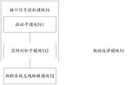
- This embodiment provides a chip, as shown in FIG. 5, including:
- the interface signal control module 51 is configured to receive a master-slave mode selection signal, wherein the master-slave mode selection signal is used to indicate that the chip is a master chip or a slave chip; when determining that the slave chip is a slave chip according to the master-slave mode selection signal , open the cascade system bus conversion module (ASRAM2BUS);
- the cascading system bus conversion module 52 is configured to receive access and control of the main chip, and cooperate with the main chip for data processing.
- the interface signal control module includes:
- a receiving submodule 511 configured to receive a master-slave mode selection signal (CC_BS);
- the logic determining sub-module 512 is configured to perform internal logic determination according to the received master-slave mode selection signal.
- the master-slave mode selection signal is 0, the chip is the master chip, and when it is not 0, the chip is the slave chip.
- the bit width value of the master-slave mode selection signal is configurable, the minimum bit width is 1, and the maximum value is set according to requirements.
- the signal is an input signal of the chip. When the value is not 0, the indicator chip is From the chip, and indicating its own number, the value of this signal is generally kept constant while the chip is operating normally.
- the chip further includes: a data selection module for transmitting a data signal (CC_DATA) to and from the main chip, for writing data by itself or reading data by the main chip;
- CC_DATA data signal
- the wide value is configurable.
- the cascaded system bus conversion module (ASRAM2BUS), as shown in FIG. 6, includes a system control register sub-module (CFGREG), a cascaded system bus conversion sub-module (ASRAM2BUS), an internal buffer sub-module (MEM), and a memory control.
- CFGREG system control register sub-module
- ASRAM2BUS cascaded system bus conversion sub-module
- MEM internal buffer sub-module
- Submodule and address mapping submodule Submodule and address mapping submodule;
- the internal cache sub-module 61 is used for buffering data and control signals
- a memory control sub-module 62 configured to control reading and writing of the internal cache module
- the address mapping sub-module 63 is configured to pre-store the address mapping table, and the address mapping table divides the main chip access from the address space of the chip into configurable fixed channels according to spatial units such as 4 KB, 16 KB, 32 KB, 64 KB, 128 KB, 1 M, and 2 M.
- the physical address of the device in the main chip is divided according to the channels.
- Each channel in the slave chip represents the starting address and space size of a physical address of the device, and the starting address of the physical address can be set to a specific The device start address, when the slave is working, the start address is configurable and the address can be reset.
- the cascaded system bus conversion module does not work.
- the cascading system bus conversion sub-module 64 is configured to receive an address signal (CC_ADDR) sent by the main chip to determine whether the chip is to be accessed by the main chip, and if so, establish contact with the main chip; the bit width value of the signal is configurable
- the signal is the output signal of the main chip in the master chip mode, and the input signal of the slave chip in the slave chip mode, the effective address of the signal is the physical space address of the master chip, and is also the physical space address of the slave chip;
- the address signal may include first data and a second data, wherein the first data is consistent with a CC_BS signal at a high or low position in the address signal, and the second data is a slave chip to be accessed by the master chip. Identification; access address space can be set to access channels according to different size capacity;
- the receiving and receiving mode (CC_CS) sent by the main chip determines its own reading and writing mode, which is a single-bit signal, which is the output signal of the main chip in the main chip mode, and the input from the chip in the slave chip mode. Signal, when the signal is low, the bus is in read or write mode, read And write mode are valid, determined by CC_WE and CC_OE signals;
- the write enable signal (CC_WE) sent by the main chip By receiving the write enable signal (CC_WE) sent by the main chip to determine whether it is in the write valid mode, it is a single bit signal, and the signal is an output signal in the main chip, for example, when the signal is low level and effective When the energy signal is low, the corresponding slave chip is set to be valid, and the phase of the signal and the CC_CS signal are configurable;
- the read enable signal (CC_OE) sent by the main chip By receiving the read enable signal (CC_OE) sent by the main chip to determine whether it is in the read enable mode, it is a single bit signal, and the signal is an output signal in the main chip, for example, when the signal is low level, and CC_CS When the signal is low, it indicates that the bus read is valid, and the phase of the signal and the CC_CS signal are configurable;
- CC_BUSY a read valid signal
- CC_BUSY Sending a read valid signal (CC_BUSY) to the main chip to notify the main chip to read its own data; it is a single bit signal, which is an input signal in the main chip, and an output signal in the slave chip, the signal is high At the level, the data sent from the chip to the main chip is valid data, and the phase relationship between the signal and the CC_CS and CC_OE signals is configurable;
- the system control register sub-module 65 is configured to perform resetting when receiving the reset signal (CC_RST) sent by the main chip, which is a single-bit signal, and the signal is an output signal in the main chip, and is an input signal in the slave chip. For example, when the signal is low, the interface bus and the registers of the device in the slave are reset.
- C_RST reset signal
- the above interconnect bus can be converted into any on-chip bus in the chip; the timing parameters of the interconnect bus can be configured; the interconnect interface bus is a simplex asynchronous interface, and has no clock signal.
- the device is provided with a device for chip interconnection, as shown in FIG. 7 , and may include: a main chip and N slave chips;
- a master chip 71 configured to receive a master-slave mode selection signal, wherein the master-slave mode selection signal is used to indicate that the chip is a master chip or a slave chip; and when determining that the master chip is the master chip according to the master-slave mode selection signal, accessing N slave chips, controlling the N slave chips, and The N slave chips cooperate to perform memory data processing; N is a positive integer greater than or equal to 1;
- the slave chip 72 is configured to receive a master-slave mode selection signal; when the second chip determines that it is a slave chip according to the master-slave mode selection signal, receiving access and control of the master chip, and performing data processing with the master chip .
- the main chip includes: an interface signal control module, configured to receive a master-slave mode selection signal, and when the main slave mode selection signal is determined to be the main chip according to the master-slave mode selection signal, the system cascade bus conversion module is turned on;
- the system cascade bus conversion module is configured to access N slave chips, and perform memory data processing with the N slave chips; N is a positive integer greater than or equal to 1.
- the interface signal control module includes:
- a receiving submodule configured to receive a master-slave mode selection signal
- the logic judging sub-module is configured to perform internal logic judgment according to the received master-slave mode selection signal, and when the master-slave mode selection signal is 0, the chip is a main chip.
- the main chip further includes: the data selection module, configured to write data to the slave chip through the data signal, or read data from the slave chip; correspondingly, the system cascade bus conversion module is further used
- the data selection module is controlled to perform read and write access selection control and loopback access data.
- the system cascade bus conversion module includes:
- An internal buffer sub-module for buffering data and control signals during system cascade bus conversion
- a memory control sub-module for controlling the read/write control function of the internal cache sub-module
- a system cascade bus conversion submodule for selecting a slave chip to be accessed by an address signal;
- the address signal includes first data and second data, the first data being consistent with a master-slave mode selection signal, located at the address a high or low bit in the signal, the second data is an identifier of the slave chip to be accessed by the master chip;
- a read/write mode of the slave chip is set by an effective enable signal; and whether the slave chip is in write by the write enable signal is set Mode; set by the read enable signal from the core Whether the slice is in the read enable mode; determining whether it is in the state of reading the slave chip data by receiving the read valid signal;
- the system control register sub-module is configured to send a reset signal to the slave chip and reset the slave chip through the reset signal.
- the system cascade bus conversion module is specifically configured to perform channel access to different address spaces from the chip, and the address space is configurable.
- the above slave chip includes:
- An interface signal control module configured to receive a master-slave mode selection signal, where the master-slave mode selection signal is used to indicate that the chip is a master chip or a slave chip; when determining that the chip is a slave chip according to the master-slave mode selection signal, Turn on the cascade system bus conversion module;
- the cascading system bus conversion module is configured to receive access and control of the main chip, and cooperate with the main chip for data processing.
- the interface signal control module includes:
- a receiving submodule configured to receive a master-slave mode selection signal
- the logic judging sub-module is configured to perform internal logic judgment according to the received master-slave mode selection signal, and when the master-slave mode selection signal is not 0, the chip is a slave chip.
- the slave chip further includes: a data selection module for transmitting data signals to and from the master chip for writing data by itself or reading data by the master chip.
- the cascading system bus conversion module includes:
- a memory control sub-module for controlling reading and writing of the internal cache module
- An address mapping sub-module configured to pre-store an address mapping table, configured to divide a configurable fixed channel according to a spatial unit from an address space of the chip;
- the cascading system bus conversion sub-module is configured to receive an address signal sent by the main chip to determine whether it is a chip to be accessed by the main chip, and if so, establish contact with the main chip;
- the effective enable signal sent by the chip determines its own read/write mode; determines whether it is in the write valid mode by receiving the write enable signal sent by the main chip; determines whether it is in read by receiving the read enable signal sent by the main chip.
- the enable mode sends a read valid signal to the main chip to notify the main chip to read its own data;
- the system control register sub-module is configured to reset when receiving a reset signal from the main chip.
- the cascading system bus conversion module is specifically configured to receive an address channel configured by the main chip, and receive the access of the main chip through the address channel.
- the cascade application is shown in Figure 8.
- the input value of the CC_BS of the master chip is 0, and the input value of the CC_BS from the chip is non-zero.
- the master-slave chip is connected through the cascade interface bus, and the maximum number of chips is the value of CC_BS minus one.
- the cascaded system bus conversion module is in an inoperative state; correspondingly, when the chip is used as a slave chip, such as from the chip 0, wherein the system is cascaded. The conversion module is not working.
- the device is described in detail below with the address width of the external cascading interface bus being 26 bits, the data bit width being 16 bits, and the master-slave mode selection signal being a 4-bit configuration mode.
- the chip cascading device of the 16-chip chip is shown in Fig. 9. Only two cascades of chips are shown in the figure, the cascade connections of the other 14 chips are similar, and so on.
- the disclosed apparatus and method may be implemented in other manners.
- the device embodiments described above are merely illustrative.
- the division of the unit is only a logical function division.
- there may be another division manner such as: multiple units or components may be combined, or Can be integrated into another system, or some features can be ignored or not executed.
- the coupling, or direct coupling, or communication connection of the components shown or discussed may be indirect coupling or communication connection through some interfaces, devices or units, and may be electrical, mechanical or other forms. of.
- the units described above as separate components may or may not be physically separated, and the components displayed as the unit may or may not be physical units, that is, may be located in one place or distributed to multiple network units; Some or all of the units may be selected according to actual needs to achieve the purpose of the solution of the embodiment.
- each functional unit in each embodiment of the present invention may be integrated into one processing unit, or each unit may be separately used as one unit, or two or more units may be integrated into one unit;
- the unit can be implemented in the form of hardware or in the form of hardware plus software functional units.
- the foregoing program may be stored in a computer readable storage medium, and the program is executed when executed.
- the foregoing storage device includes the following steps: the foregoing storage medium includes: a mobile storage device, a read-only memory (ROM), a random access memory (RAM), a magnetic disk, or an optical disk.
- ROM read-only memory
- RAM random access memory
- magnetic disk or an optical disk.
- optical disk A medium that can store program code.
- the above-described integrated unit of the present invention may be stored in a computer readable storage medium if it is implemented in the form of a software function module and sold or used as a standalone product.
- the technical solution of the embodiments of the present invention may be embodied in the form of a software product in essence or in the form of a software product stored in a storage medium, including a plurality of instructions.
- a computer device (which may be a personal computer, server, or network device, etc.) is caused to perform all or part of the methods described in various embodiments of the present invention.
- the foregoing storage medium includes: a removable storage device, a read-only memory (ROM), a random access memory (RAM), a magnetic disk, or an optical disk, and the like, which can store program codes.
- the invention discloses a chip interconnection method, a chip and a device, which can determine a chip as a main chip or a slave chip according to a received master-slave mode selection signal, and can work together by the master chip and the slave chip to enable integration of the chip.
- the business processing capability is enhanced, the chip utilization rate is improved, and the market competitiveness of the chip application system is further improved.
Landscapes
- Engineering & Computer Science (AREA)
- Theoretical Computer Science (AREA)
- General Engineering & Computer Science (AREA)
- Physics & Mathematics (AREA)
- General Physics & Mathematics (AREA)
- Computer Hardware Design (AREA)
- Mathematical Physics (AREA)
- Logic Circuits (AREA)
- Bus Control (AREA)
Abstract
本发明公开了一种芯片互连的方法、芯片及装置,其中方法包括:接收主从模式选择信号;其中,所述主从模式选择信号用于指示芯片为主芯片或从芯片;当根据所述主从模式选择信号确定自身为主芯片时,访问N个从芯片,对所述N个从芯片进行控制、并且与所述N个从芯片配合进行内存数据处理;N为大于等于1的正整数。
Description
本发明涉及通信领域的芯片技术,尤其涉及一种芯片互连的方法、芯片及装置。
随着无线和有线技术的迅速发展,业务处理能力成倍增长,对系统核心芯片的规模和处理能力提出了更高的要求,但是受到加工工艺、芯片功耗和成本的限制,芯片不能无限制的增大其设计规模,这就迫切要求在业务处理能力巨大增长下,需要提高芯片的处理能力,目前业界的方案主要是增大芯片的设计规模,但是,这样在一定程度上都提高了芯片的设计成本和技术难度,增加了芯片的功耗。
发明内容
有鉴于此,本发明实施例的主要目的在于提供一种芯片互连的方法、芯片及装置,至少解决了现有技术中存在的上述问题。
本发明实施例提供了一种芯片互连的方法,所述方法包括:
接收主从模式选择信号;其中,所述主从模式选择信号用于指示芯片为主芯片或从芯片;
当根据所述主从模式选择信号确定自身为主芯片时,访问N个从芯片,对所述N个从芯片进行控制、并且与所述N个从芯片配合进行内存数据处理;N为大于等于1的正整数。
上述方案中,所述根据所述主从模式选择信号确定自身为主芯片包括:当接收到的主从模式选择信号中的值为0时,确定自身为主芯片;当接收
到主从模式选择信号中的值非0时,确定自身为从芯片。
上述方案中,所述与所述N个从芯片配合进行内存数据处理包括:通过数据信号向从芯片写入数据、或在从芯片中读取数据。
上述方案中,对所述N个从芯片进行控制包括以下操作至少之一:
通过地址信号选取所要访问的从芯片;所述地址信号包括第一数据和第二数据,所述第一数据与主从模式选择信号一致,位于所述地址信号中的高位或低位,所述第二数据为所述主芯片所要访问的从芯片的标识;
通过有效使能信号设置从芯片的读写模式;
通过写使能信号设置从芯片是否处于写有效模式;
通过读使能信号设置从芯片是否处于读使能模式;
通过接收读有效信号,确定自身是否处于读取从芯片数据的状态;
通过复位信号对从芯片进行复位。
上述方案中,所述访问N个从芯片为:对从芯片进行不同地址空间的通道访问,所述地址空间可配置。
本发明实施例还提供了一种芯片互连的方法,所述方法包括:
接收主从模式选择信号;其中,所述主从模式选择信号用于指示芯片为主芯片或从芯片;
当根据所述主从模式选择信号确定自身为从芯片时,接收主芯片的访问及控制,并且与主芯片配合进行数据处理。
上述方案中,所述根据所述主从模式选择信号确定自身为主芯片包括:当接收到主从模式选择信号中的值非0时,确定自身为从芯片。
上述方案中,所述与主芯片配合进行数据处理包括:与主芯片相互传输数据信号,用以在自身写入数据、或由主芯片读取数据。
上述方案中,所述接收主芯片的访问及控制包括以下操作至少之一:
接收主芯片发来的地址信号,根据所述地址信号的第二数据中的从芯
片的标识,判断自身是否为主芯片所要访问的芯片,若是,则与主芯片建立联系;
通过接收主芯片发来的有效使能信号确定自身的读写模式;
通过接收主芯片发来的写使能信号确定自身是否处于写有效模式;
通过接收主芯片发来的读使能信号确定自身是否处于读使能模式;
向主芯片发送读有效信号,用以通知所述主芯片读取自身数据;
根据主芯片发来的复位信号,进行复位。
上述方案中,所述方法还包括:接收主芯片配置的地址通道,并通过所述地址通道接收主芯片的访问。
本发明实施例提供了一种芯片,所述芯片包括:
接口信号控制模块,用于接收主从模式选择信号,当根据所述主从模式选择信号确定自身为主芯片时,开启系统级联总线转换模块;
系统级联总线转换模块,用于访问N个从芯片,与所述N个从芯片配合进行内存数据处理;N为大于等于1的正整数。
上述方案中,所述接口信号控制模块,包括:
接收子模块,用于接收主从模式选择信号;
逻辑判断子模块,用于根据接收的主从模式选择信号进行内部逻辑判断,当该主从模式选择信号为0时表示芯片是主芯片。
上述方案中,所述芯片还包括:所述数据选择模块,用于通过数据信号向从芯片写入数据、或从任意一个从芯片中读取数据;
相应的,所述系统级联总线转换模块,还用于控制所述数据选择模块进行读写访问选择控制和环回访问数据。
上述方案中,所述系统级联总线转换模块,包括:
内部缓存子模块,用于缓存系统级联总线转换时的数据和控制信号;
内存控制子模块,用于控制内部缓存子模块的读写控制功能;
系统级联总线转换子模块,用于通过地址信号选取所要访问的从芯片;所述地址信号包括第一数据和第二数据,所述第一数据与主从模式选择信号一致,位于所述地址信号中的高位或低位,所述第二数据为所述主芯片所要访问的从芯片的标识;通过有效使能信号设置从芯片的读写模式;通过写使能信号设置从芯片是否处于写有效模式;通过读使能信号设置从芯片是否处于读使能模式;通过接收读有效信号,确定自身是否处于读取从芯片数据的状态;向从芯片发送复位信号,通过复位信号对从芯片进行复位。
上述方案中,所述系统级联总线转换模块,具体用于对从芯片进行不同地址空间的通道访问,所述地址空间可配置。
本发明还提供了一种芯片,所述芯片包括:
接口信号控制模块,用于接收主从模式选择信号;其中,所述主从模式选择信号用于指示芯片为主芯片或从芯片;当根据所述主从模式选择信号确定自身为从芯片时,开启级联系统总线转换模块;
级联系统总线转换模块,用于接收主芯片的访问及控制,并且与主芯片配合进行数据处理。
上述方案中,所述接口信号控制模块,包括:
接收子模块,用于接收主从模式选择信号;
逻辑判断子模块,用于根据接收的主从模式选择信号进行内部逻辑判断,当该主从模式选择信号不为0时表示芯片是从芯片。
上述方案中,所述芯片还包括:数据选择模块,用于与主芯片相互传输数据信号,用以在自身写入数据、或由主芯片读取数据。
上述方案中,所述级联系统总线转换模块,包括:
内部缓存子模块,用于数据和控制信号的缓存;
内存控制子模块,用于控制内部缓存模块的读写;
地址映射子模块,用于预存地址映射表,用于将从芯片的地址空间按照空间单元划分了可配置的固定通道;
级联系统总线转换子模块,用于接收主芯片发来的地址信号判断自身是否为主芯片所要访问的芯片,若是,则与主芯片建立联系;通过接收主芯片发来的有效使能信号确定自身的读写模式;通过接收主芯片发来的写使能信号确定自身是否处于写有效模式;通过接收主芯片发来的读使能信号确定自身是否处于读使能模式;向主芯片发送读有效信号,用以通知所述主芯片读取自身数据;
系统控制寄存器子模块,用于当接收到主芯片发来的复位信号时,进行复位。
上述方案中,所述级联系统总线转换模块,具体用于接收主芯片配置的地址通道,并通过所述地址通道接收主芯片的访问。
本发明实施例还提供了一种芯片互连的装置,所述装置包括:主芯片及N个从芯片,N为大于等于1的正整数;其中,
主芯片,用于接收主从模式选择信号;其中,所述主从模式选择信号用于指示芯片为主芯片或从芯片;当根据所述主从模式选择信号确定自身为主芯片时,访问N个从芯片,对所述N个从芯片进行控制、并且与所述N个从芯片配合进行内存数据处理;
从芯片,用于接收主从模式选择信号;当所述第二芯片根据所述主从模式选择信号确定自身为从芯片时,接收主芯片的访问及控制,并且与主芯片配合进行数据处理。
上述方案中,所述主芯片包括:
接口信号控制模块,用于接收主从模式选择信号,当根据所述主从模式选择信号确定自身为主芯片时,开启系统级联总线转换模块;
系统级联总线转换模块,用于访问N个从芯片,与所述N个从芯片配
合进行内存数据处理;N为大于等于1的正整数。
上述方案中,所述接口信号控制模块,包括:
接收子模块,用于接收主从模式选择信号;
逻辑判断子模块,用于根据接收的主从模式选择信号进行内部逻辑判断,当该主从模式选择信号为0时表示芯片是主芯片。
上述方案中,所述主芯片还包括:所述数据选择模块,用于通过数据信号向从芯片写入数据、或从任意一个从芯片中读取数据;相应的,所述系统级联总线转换模块,还用于控制所述数据选择模块进行读写访问选择控制和环回访问数据。
上述方案中,所述系统级联总线转换模块,包括:
内部缓存子模块,用于缓存系统级联总线转换时的数据和控制信号;
内存控制子模块,用于控制内部缓存子模块的读写控制功能;
系统级联总线转换子模块,用于通过地址信号选取所要访问的从芯片;所述地址信号包括第一数据和第二数据,所述第一数据与主从模式选择信号一致,位于所述地址信号中的高位或低位,所述第二数据为所述主芯片所要访问的从芯片的标识;通过有效使能信号设置从芯片的读写模式;通过写使能信号设置从芯片是否处于写有效模式;通过读使能信号设置从芯片是否处于读使能模式;通过接收读有效信号,确定自身是否处于读取从芯片数据的状态;
系统控制寄存器子模块,用于向从芯片发送复位信号,通过复位信号对从芯片进行复位。
上述方案中,所述系统级联总线转换模块,具体用于对从芯片进行不同地址空间的通道访问,所述地址空间可配置。
上述方案中,所述从芯片包括:
接口信号控制模块,用于接收主从模式选择信号;其中,所述主从模
式选择信号用于指示芯片为主芯片或从芯片;当根据所述主从模式选择信号确定自身为从芯片时,开启级联系统总线转换模块;
级联系统总线转换模块,用于接收主芯片的访问及控制,并且与主芯片配合进行数据处理。
上述方案中,所述接口信号控制模块,包括:
接收子模块,用于接收主从模式选择信号;
逻辑判断子模块,用于根据接收的主从模式选择信号进行内部逻辑判断,当该主从模式选择信号不为0时表示芯片是从芯片。
上述方案中,所述从芯片还包括:数据选择模块,用于与主芯片相互传输数据信号,用以在自身写入数据、或由主芯片读取数据。
上述方案中,所述级联系统总线转换模块,包括:
内部缓存子模块,用于数据和控制信号的缓存;
内存控制子模块,用于控制内部缓存模块的读写;
地址映射子模块,用于预存地址映射表,用于将从芯片的地址空间按照空间单元划分了可配置的固定通道;
级联系统总线转换子模块,用于接收主芯片发来的地址信号判断自身是否为主芯片所要访问的芯片,若是,则与主芯片建立联系;通过接收主芯片发来的有效使能信号确定自身的读写模式;通过接收主芯片发来的写使能信号确定自身是否处于写有效模式;通过接收主芯片发来的读使能信号确定自身是否处于读使能模式;向主芯片发送读有效信号,用以通知所述主芯片读取自身数据;
系统控制寄存器子模块,用于当接收到主芯片发来的复位信号时,进行复位。
上述方案中,所述级联系统总线转换模块,具体用于接收主芯片配置的地址通道,并通过所述地址通道接收主芯片的访问。
本发明实施例所提供的芯片互连的方法、芯片及装置,能够通过设置主芯片以及从芯片,并且通过主芯片与从芯片协同工作,可使得芯片的综合业务处理能力增强,提高芯片利用率,进而提高芯片所应用系统市场竞争力。
图1为本发明实施例芯片互连的方法流程示意图一;
图2为本发明实施例芯片互连的方法流程示意图二;
图3为本发明实施例芯片组成结构示意图一;
图4为本发明实施例芯片中系统级联总线转换模块组成结构示意图;
图5为本发明实施例芯片组成结构示意图二;
图6为本发明实施例芯片中级联系统总线转换模块组成结构示意图;
图7为本发明实施例芯片互连的装置组成结构示意图;
图8为本发明实施例芯片互连场景示意一;
图9为本发明实施例芯片互连场景示意二。
下面结合附图及具体实施例对本发明再作进一步详细的说明。
实施例一、
本发明实施例提供了一种芯片互连的方法,如图1所示,包括:
步骤101:接收主从模式选择信号;其中,所述主从模式选择信号用于指示芯片为主芯片或从芯片。
步骤102:当根据所述主从模式选择信号确定自身为主芯片时,访问N个从芯片,对所述N个从芯片进行控制、并且与所述N个从芯片配合进行内存数据处理;N为大于等于1的正整数。
这里,所述接收主从模式选择信号包括:所述第一芯片中的主从模式
设置管脚,通过互连总线接收主从模式选择信号(CC_BS);
其中,所述主从模式选择信号的位宽值可配置,位宽最小值为1,最大值根据需要进行设置,该信号为所述芯片的输入信号,当值为0时,指示芯片为主芯片,当其值非0时,指示芯片为从芯片,并且指示该从芯片的编号,该信号的值一般在芯片正常工作时保持恒定。
其中,所述第一芯片根据所述主从模式选择信号确定自身为主芯片可以包括:当接收到的主从模式选择信号中的值为0时,确定自身为主芯片;当接收到主从模式选择信号中的值非0时,确定自身为从芯片。
所述访问N个从芯片为:对从芯片进行不同地址空间的通道访问,所述地址空间可配置;主芯片通过配置的N个地址通道分别访问对应的N个从芯片,所述地址通道为可配置的。
所述与所述N个从芯片配合进行数据处理可以包括:通过数据信号(CC_DATA)向从芯片写入数据、或从任意一个从芯片中读取数据;该信号的位宽值可配置,该信号实现主芯片片内总线数据和从芯片内总线的数据传输,主芯片写入从芯片的数据是主芯片的读出数据,主芯片从从芯片的读出数据是主芯片的写入数据。
优选地,对所述N个从芯片进行控制包括以下操作至少之一:
通过地址信号(CC_ADDR)选取所要访问的从芯片;该信号的位宽值可配置,该信号在主芯片模式中是主芯片的输出信号,在从芯片模式中是从芯片的输入信号,该信号的有效地址是主芯片的物理空间地址,也是从芯片的物理空间地址;所述地址信号中可以包括第一数据和第二数据,所述第一数据与CC_BS信号保持一致位于所述地址信号中的高位或低位,所述第二数据为所述主芯片所要访问的从芯片的标识;进而,通过发送地址信号就可以使得从芯片判断主芯片是否要访问自身,从而将主从的芯片的访问联系起来;
通过有效使能信号(CC_CS)设置从芯片的读写模式,为单bit信号,该信号在主芯片模式中是主芯片的输出信号,在从芯片模式中是从芯片的输入信号,该信号为低电平时表示总线处于读或写模式,读和写模式有效,由CC_WE和CC_OE信号决定;
通过写使能信号(CC_WE)设置从芯片是否处于写有效模式,为单bit信号,该信号在主芯片中是输出信号,比如,当该信号为低电平、且有效使能信号为低电平时,设置对应的从芯片为写有效,该信号和CC_CS信号的相位是可以配置的;
通过读使能信号(CC_OE)设置从芯片是否处于读使能模式,为单bit信号,该信号在主芯片中是输出信号,比如,当该信号为低电平、且CC_CS信号为低电平时,表示总线的读有效,该信号和CC_CS信号的相位是可以配置的;
通过接收读有效信号(CC_BUSY),确定自身是否处于读取从芯片数据的状态;是单bit信号,该信号在主芯片中是输入信号,在从芯片中是输出信号,该信号为高电平时,表示从芯片送到主芯片的数据是有效数据,该信号和CC_CS、CC_OE信号的相位关系是可以配置的;
通过复位信号(CC_RST)对从芯片进行复位,是单bit信号,该信号在主芯片中是输出信号,在从片中是输入信号,比如,该信号为低电平时,复位该接口总线和从芯片中的该装置的寄存器等配置。
上述互联总线在芯片中可以和任意片内总线进行转换;互联总线的时序参数可以配置;该互联接口总线是单工异步接口,无时钟信号。
实施例二、
本实施例提供了一种芯片互连的方法,如图2所示,包括:
步骤201:接收主从模式选择信号;其中,所述主从模式选择信号用于指示芯片为主芯片或从芯片。
步骤202:当根据所述主从模式选择信号确定自身为从芯片时,接收主芯片的访问及控制,并且与主芯片配合进行数据处理。
这里,所述接收主从模式选择信号包括:所述第二芯片中的主从模式设置管脚,通过互连总线接收主从模式选择信号(CC_BS);
其中,所述主从模式选择信号的位宽值可配置,位宽最小值为1,最大值根据需要进行设置,该信号为所述芯片的输入信号,当值为0时,指示芯片为主芯片,当其值非0时,指示芯片为从芯片,并且指示该从芯片的编号,该信号的值一般在芯片正常工作时保持恒定。
其中,所述根据所述主从模式选择信号确定自身为主芯片可以包括:当接收到主从模式选择信号中的值非0时,确定自身为从芯片。
所述与主芯片配合进行数据处理可以包括:与主芯片相互传输数据信号(CC_DATA),用以在自身写入数据、或由主芯片读取数据;该信号的位宽值可配置。
优选地,接收主芯片的访问及控制包括以下操作至少之一:
接收主芯片发来的地址信号(CC_ADDR)判断自身是否为主芯片所要访问的芯片,若是,则与主芯片建立联系;该信号的位宽值可配置,该信号在主芯片模式中是主芯片的输出信号,在从芯片模式中是从芯片的输入信号,该信号的有效地址是主芯片的物理空间地址,也是从芯片的物理空间地址;所述地址信号中可以包括第一数据和第二数据,所述第一数据与CC_BS信号保持一致位于所述地址信号中的高位或低位,所述第二数据为所述主芯片所要访问的从芯片的标识;
通过接收主芯片发来的有效使能信号(CC_CS)确定自身的读写模式,为单bit信号,该信号在主芯片模式中是主芯片的输出信号,在从芯片模式中是从芯片的输入信号,该信号为低电平时表示总线处于读或写模式,读和写模式有效,由CC_WE和CC_OE信号决定;
通过接收主芯片发来的写使能信号(CC_WE)确定自身是否处于写有效模式,为单bit信号,该信号在主芯片中是输出信号,比如,当该信号为低电平、且有效使能信号为低电平时,设置对应的从芯片为写有效,该信号和CC_CS信号的相位是可以配置的;
通过接收主芯片发来的读使能信号(CC_OE)确定自身是否处于读使能模式,为单bit信号,该信号在主芯片中是输出信号,比如,当该信号为低电平、且CC_CS信号为低电平时,表示总线的读有效,该信号和CC_CS信号的相位是可以配置的;
向主芯片发送读有效信号(CC_BUSY),用以通知所述主芯片读取自身数据;是单bit信号,该信号在主芯片中是输入信号,在从芯片中是输出信号,该信号为高电平时,表示从芯片送到主芯片的数据是有效数据,该信号和CC_CS、CC_OE信号的相位关系是可以配置的;
根据主芯片发来的复位信号(CC_RST),进行复位,是单bit信号,该信号在主芯片中是输出信号,在从片中是输入信号,比如,该信号为低电平时,复位该接口总线和从芯片中的该装置的寄存器等配置。
所述方法还包括:预设地址通道,对应访问地址空间,所述访问地址空间可以按照不同大小的容量设置访问通道。
上述互联总线在芯片中可以和任意片内总线进行转换;互联总线的时序参数可以配置;该互联接口总线是单工异步接口,无时钟信号。
实施例三、
本实施例提供了一种芯片,如图3所示,包括:
接口信号控制模块31(IO_CTRL),用于接收主从模式选择信号,当根据所述主从模式选择信号确定自身为主芯片时,开启系统级联总线转换模块;
系统级联总线转换模块32(BUS2ASRAM),用于访问N个从芯片,
与所述N个从芯片配合进行内存数据处理;N为大于等于1的正整数。
所述接口信号控制模块31,包括:
接收子模块311,用于接收主从模式选择信号(CC_BS);
逻辑判断子模块312,用于根据接收的主从模式选择信号进行内部逻辑判断,当该主从模式选择信号为0时表示芯片是主芯片,不为0时表示芯片是从芯片。
所述系统级联总线转换模块32(BUS2ASRAM)实现该装置的一些基本配置功能,包括装置的环回访问控制配置、外部级联接口总线读写控制信号的相位控制参数配置等功能。并提供通过系统总线向外部级联总线的转换功能,支持任何系统总线,如AMBA总线的AXI、AHB和APB总线等。组成如图2所示。
所述芯片还包括:数据选择模块33,用于当所述芯片作为主芯片时,向从芯片写入数据、或从任意一个从芯片中读取数据;相应的,所述系统级联总线转换模块,还用于控制所述数据选择模块进行读写访问选择控制和环回访问数据。
所述系统级联总线转换模块,如图4所示,包括:系统控制寄存器子模块(CFGREG)、系统级联总线转换子模块(BUS2ASRAM)、内部缓存子模块(MEM)和内存控制子模块。
内部缓存子模块41,用于缓存系统级联总线转换时的数据和控制信号;缓存的数据足够一个burst长度,或一定长度时系统级联总线转换子模块43可以读取;
内存控制子模块42,用于控制内部缓存子模块41的读写控制功能;
系统级联总线转换子模块43(BUS2ASRAM),用于通过地址信号(CC_ADDR)选取所要访问的从芯片;该信号的位宽值可配置,该信号在主芯片模式中是主芯片的输出信号,在从芯片模式中是从芯片的输入信号,
该信号的有效地址是主芯片的物理空间地址,也是从芯片的物理空间地址;所述地址信号中可以包括第一数据和第二数据,所述第一数据与CC_BS信号保持一致位于所述地址信号中的高位或低位,所述第二数据为所述主芯片所要访问的从芯片的标识;通过发送地址信号就可以使得从芯片判断主芯片是否要访问自身,从而将主从的芯片的访问联系起来;
通过有效使能信号(CC_CS)设置从芯片的读写模式,为单bit信号,该信号在主芯片模式中是主芯片的输出信号,在从芯片模式中是从芯片的输入信号,该信号为低电平时表示总线处于读或写模式,读和写模式有效,由CC_WE和CC_OE信号决定;
通过写使能信号(CC_WE)设置从芯片是否处于写有效模式,为单bit信号,该信号在主芯片中是输出信号,比如,当该信号为低电平、且有效使能信号为低电平时,设置对应的从芯片为写有效,该信号和CC_CS信号的相位是可以配置的;
通过读使能信号(CC_OE)设置从芯片是否处于读使能模式,为单bit信号,该信号在主芯片中是输出信号,比如,当该信号为低电平、且CC_CS信号为低电平时,表示总线的读有效,该信号和CC_CS信号的相位是可以配置的;
通过接收读有效信号(CC_BUSY),确定自身是否处于读取从芯片数据的状态;是单bit信号,该信号在主芯片中是输入信号,在从芯片中是输出信号,该信号为高电平时,表示从芯片送到主芯片的数据是有效数据,该信号和CC_CS、CC_OE信号的相位关系是可以配置的;
向从芯片发送复位信号,通过复位信号(CC_RST)对从芯片进行复位,是单bit信号,该信号在主芯片中是输出信号,在从片中是输入信号,比如,该信号为低电平时,复位该接口总线和从芯片中的寄存器等配置。
所述系统控制寄存器子模块,用于获取主芯片的配置。
所述数据选择模块,具体用于通过数据信号(CC_DATA)向从芯片写入数据、或从任意一个从芯片中读取数据;该信号的位宽值可配置,该信号实现主芯片片内总线数据和从芯片内总线的数据传输,主芯片写入从芯片的数据是主芯片的读出数据,主芯片从从芯片的读出数据是主芯片的写入数据。
优选地,所述芯片还可以具备级联系统总线转换模块,但是,当所述芯片作为主芯片时,所述级联系统总线转换模块是不工作的。
实施例四、
本实施例提供了一种芯片,如图5所示,包括:
接口信号控制模块51,用于接收主从模式选择信号;其中,所述主从模式选择信号用于指示芯片为主芯片或从芯片;当根据所述主从模式选择信号确定自身为从芯片时,开启级联系统总线转换模块(ASRAM2BUS);
级联系统总线转换模块52,用于接收主芯片的访问及控制,并且与主芯片配合进行数据处理。
所述接口信号控制模块,包括:
接收子模块511,用于接收主从模式选择信号(CC_BS);
逻辑判断子模块512,用于根据接收的主从模式选择信号进行内部逻辑判断,当该主从模式选择信号为0时表示芯片是主芯片,不为0时表示芯片是从芯片。
其中,所述主从模式选择信号的位宽值可配置,位宽最小值为1,最大值根据需要进行设置,该信号为所述芯片的输入信号,当其值非0时,指示芯片为从芯片,并且指示了自身的编号,该信号的值一般在芯片正常工作时保持恒定。
所述芯片还包括:数据选择模块,用于与主芯片相互传输数据信号(CC_DATA),用以在自身写入数据、或由主芯片读取数据;该信号的位
宽值可配置。
优选地,级联系统总线转换模块(ASRAM2BUS),如图6所示,包括系统控制寄存器子模块(CFGREG)、级联系统总线转换子模块(ASRAM2BUS)、内部缓存子模块(MEM)、内存控制子模块和地址映射子模块;
内部缓存子模块61用于数据和控制信号的缓存;
内存控制子模块62,用于控制内部缓存模块的读写;
地址映射子模块63,用于预存地址映射表,该地址映射表将主芯片访问从芯片的地址空间按照4KB、16KB、32KB、64KB、128KB、1M和2M等空间单元划分了可配置的固定通道,将主芯片中的该装置物理地址按这些通道划分,在从芯片中每个通道代表了一个设备的物理地址的起始地址和空间大小,该物理地址的起始地址可以设置为一个具体的设备起始地址,从芯片工作时,该起始地址是可配置的,该地址可以被复位。
在主芯片中,级联系统总线转换模块是不工作的。
级联系统总线转换子模块64,用于接收主芯片发来的地址信号(CC_ADDR)判断自身是否为主芯片所要访问的芯片,若是,则与主芯片建立联系;该信号的位宽值可配置,该信号在主芯片模式中是主芯片的输出信号,在从芯片模式中是从芯片的输入信号,该信号的有效地址是主芯片的物理空间地址,也是从芯片的物理空间地址;所述地址信号中可以包括第一数据和第二数据,所述第一数据与CC_BS信号保持一致位于所述地址信号中的高位或低位,所述第二数据为所述主芯片所要访问的从芯片的标识;访问地址空间可以按照不同大小的容量设置访问通道;
通过接收主芯片发来的有效使能信号(CC_CS)确定自身的读写模式,为单bit信号,该信号在主芯片模式中是主芯片的输出信号,在从芯片模式中是从芯片的输入信号,该信号为低电平时表示总线处于读或写模式,读
和写模式有效,由CC_WE和CC_OE信号决定;
通过接收主芯片发来的写使能信号(CC_WE)确定自身是否处于写有效模式,为单bit信号,该信号在主芯片中是输出信号,比如,当该信号为低电平、且有效使能信号为低电平时,设置对应的从芯片为写有效,该信号和CC_CS信号的相位是可以配置的;
通过接收主芯片发来的读使能信号(CC_OE)确定自身是否处于读使能模式,为单bit信号,该信号在主芯片中是输出信号,比如,当该信号为低电平、且CC_CS信号为低电平时,表示总线的读有效,该信号和CC_CS信号的相位是可以配置的;
向主芯片发送读有效信号(CC_BUSY),用以通知所述主芯片读取自身数据;是单bit信号,该信号在主芯片中是输入信号,在从芯片中是输出信号,该信号为高电平时,表示从芯片送到主芯片的数据是有效数据,该信号和CC_CS、CC_OE信号的相位关系是可以配置的;
系统控制寄存器子模块65,用于当接收到主芯片发来的复位信号(CC_RST)时,进行复位,是单bit信号,该信号在主芯片中是输出信号,在从片中是输入信号,比如,该信号为低电平时,复位该接口总线和从芯片中的该装置的寄存器等配置。
上述互联总线在芯片中可以和任意片内总线进行转换;互联总线的时序参数可以配置;该互联接口总线是单工异步接口,无时钟信号。
实施例五、
基于上述芯片互联的方法以及芯片,本实施例提供了一种芯片互连的装置,如图7所示,可以包括:主芯片及N个从芯片;
主芯片71,用于接收主从模式选择信号;其中,所述主从模式选择信号用于指示芯片为主芯片或从芯片;当根据所述主从模式选择信号确定自身为主芯片时,访问N个从芯片,对所述N个从芯片进行控制、并且与所
述N个从芯片配合进行内存数据处理;N为大于等于1的正整数;
从芯片72,用于接收主从模式选择信号;当所述第二芯片根据所述主从模式选择信号确定自身为从芯片时,接收主芯片的访问及控制,并且与主芯片配合进行数据处理。
其中,所述主芯片包括:接口信号控制模块,用于接收主从模式选择信号,当根据所述主从模式选择信号确定自身为主芯片时,开启系统级联总线转换模块;
系统级联总线转换模块,用于访问N个从芯片,与所述N个从芯片配合进行内存数据处理;N为大于等于1的正整数。
所述接口信号控制模块,包括:
接收子模块,用于接收主从模式选择信号;
逻辑判断子模块,用于根据接收的主从模式选择信号进行内部逻辑判断,当该主从模式选择信号为0时表示芯片是主芯片。
所述主芯片还包括:所述数据选择模块,用于通过数据信号向从芯片写入数据、或从任意一个从芯片中读取数据;相应的,所述系统级联总线转换模块,还用于控制所述数据选择模块进行读写访问选择控制和环回访问数据。
所述系统级联总线转换模块,包括:
内部缓存子模块,用于缓存系统级联总线转换时的数据和控制信号;
内存控制子模块,用于控制内部缓存子模块的读写控制功能;
系统级联总线转换子模块,用于通过地址信号选取所要访问的从芯片;所述地址信号包括第一数据和第二数据,所述第一数据与主从模式选择信号一致,位于所述地址信号中的高位或低位,所述第二数据为所述主芯片所要访问的从芯片的标识;通过有效使能信号设置从芯片的读写模式;通过写使能信号设置从芯片是否处于写有效模式;通过读使能信号设置从芯
片是否处于读使能模式;通过接收读有效信号,确定自身是否处于读取从芯片数据的状态;
系统控制寄存器子模块,用于向从芯片发送复位信号,通过复位信号对从芯片进行复位。
所述系统级联总线转换模块,具体用于对从芯片进行不同地址空间的通道访问,所述地址空间可配置。
另外,上述从芯片包括:
接口信号控制模块,用于接收主从模式选择信号;其中,所述主从模式选择信号用于指示芯片为主芯片或从芯片;当根据所述主从模式选择信号确定自身为从芯片时,开启级联系统总线转换模块;
级联系统总线转换模块,用于接收主芯片的访问及控制,并且与主芯片配合进行数据处理。
所述接口信号控制模块,包括:
接收子模块,用于接收主从模式选择信号;
逻辑判断子模块,用于根据接收的主从模式选择信号进行内部逻辑判断,当该主从模式选择信号不为0时表示芯片是从芯片。
所述从芯片还包括:数据选择模块,用于与主芯片相互传输数据信号,用以在自身写入数据、或由主芯片读取数据。
所述级联系统总线转换模块,包括:
内部缓存子模块,用于数据和控制信号的缓存;
内存控制子模块,用于控制内部缓存模块的读写;
地址映射子模块,用于预存地址映射表,用于将从芯片的地址空间按照空间单元划分了可配置的固定通道;
级联系统总线转换子模块,用于接收主芯片发来的地址信号判断自身是否为主芯片所要访问的芯片,若是,则与主芯片建立联系;通过接收主
芯片发来的有效使能信号确定自身的读写模式;通过接收主芯片发来的写使能信号确定自身是否处于写有效模式;通过接收主芯片发来的读使能信号确定自身是否处于读使能模式;向主芯片发送读有效信号,用以通知所述主芯片读取自身数据;
系统控制寄存器子模块,用于当接收到主芯片发来的复位信号时,进行复位。
所述级联系统总线转换模块,具体用于接收主芯片配置的地址通道,并通过所述地址通道接收主芯片的访问。
级联应用如图8所示。在级联应用时,主芯片的CC_BS的输入值为0,从芯片的CC_BS输入值为非0。主从芯片通过级联接口总线进行连接,从芯片的最大数目是CC_BS的值减去1。另外,通过图8可以直观的看到,当芯片作为主芯片时,其级联系统总线转换模块处于不工作状态;相应的,当芯片作为从芯片时,如从芯片0,其中系统级联总线转换模块处于不工作状态。
下面以外部级联接口总线的地址位宽为26bit,数据位宽为16bit,主从模式选择信号为4bit的配置模式,对该装置进行详细描述。
16组芯片的芯片级联装置装置如图9所示,图中只画出了2个芯片的级联,其它14个芯片的级联连接相似,以此类推。
在本申请所提供的几个实施例中,应该理解到,所揭露的设备和方法,可以通过其它的方式实现。以上所描述的设备实施例仅仅是示意性的,例如,所述单元的划分,仅仅为一种逻辑功能划分,实际实现时可以有另外的划分方式,如:多个单元或组件可以结合,或可以集成到另一个系统,或一些特征可以忽略,或不执行。另外,所显示或讨论的各组成部分相互之间的耦合、或直接耦合、或通信连接可以是通过一些接口,设备或单元的间接耦合或通信连接,可以是电性的、机械的或其它形式的。
上述作为分离部件说明的单元可以是、或也可以不是物理上分开的,作为单元显示的部件可以是、或也可以不是物理单元,即可以位于一个地方,也可以分布到多个网络单元上;可以根据实际的需要选择其中的部分或全部单元来实现本实施例方案的目的。
另外,在本发明各实施例中的各功能单元可以全部集成在一个处理单元中,也可以是各单元分别单独作为一个单元,也可以两个或两个以上单元集成在一个单元中;上述集成的单元既可以采用硬件的形式实现,也可以采用硬件加软件功能单元的形式实现。
本领域普通技术人员可以理解:实现上述方法实施例的全部或部分步骤可以通过程序指令相关的硬件来完成,前述的程序可以存储于一计算机可读取存储介质中,该程序在执行时,执行包括上述方法实施例的步骤;而前述的存储介质包括:移动存储设备、只读存储器(ROM,Read-Only Memory)、随机存取存储器(RAM,Random Access Memory)、磁碟或者光盘等各种可以存储程序代码的介质。
或者,本发明上述集成的单元如果以软件功能模块的形式实现并作为独立的产品销售或使用时,也可以存储在一个计算机可读取存储介质中。基于这样的理解,本发明实施例的技术方案本质上或者说对现有技术做出贡献的部分可以以软件产品的形式体现出来,该计算机软件产品存储在一个存储介质中,包括若干指令用以使得一台计算机设备(可以是个人计算机、服务器、或者网络设备等)执行本发明各个实施例所述方法的全部或部分。而前述的存储介质包括:移动存储设备、只读存储器(ROM,Read-Only Memory)、随机存取存储器(RAM,Random Access Memory)、磁碟或者光盘等各种可以存储程序代码的介质。
以上所述,仅为本发明的具体实施方式,但本发明的保护范围并不局限于此,任何熟悉本技术领域的技术人员在本发明揭露的技术范围内,可
轻易想到变化或替换,都应涵盖在本发明的保护范围之内。因此,本发明的保护范围应以所述权利要求的保护范围为准。
本发明公开了一种芯片互连的方法、芯片及装置,能够根据接收到的主从模式选择信号确定芯片为主芯片或从芯片,并且通过主芯片与从芯片协同工作,可使得芯片的综合业务处理能力增强,提高芯片利用率,进而提高芯片所应用系统市场竞争力。
Claims (31)
- 一种芯片互连的方法,所述方法包括:接收主从模式选择信号;其中,所述主从模式选择信号用于指示芯片为主芯片或从芯片;当根据所述主从模式选择信号确定自身为主芯片时,访问N个从芯片,对所述N个从芯片进行控制、并且与所述N个从芯片配合进行内存数据处理;N为大于等于1的正整数。
- 根据权利要求1所述的方法,其中,所述根据所述主从模式选择信号确定自身为主芯片,包括:当接收到的主从模式选择信号中的值为0时,确定自身为主芯片;当接收到主从模式选择信号中的值非0时,确定自身为从芯片。
- 根据权利要求1所述的方法,其中,所述与所述N个从芯片配合进行内存数据处理,包括:通过数据信号向从芯片写入数据、或在从芯片中读取数据。
- 根据权利要求1所述的方法,其中,对所述N个从芯片进行控制包括以下操作至少之一:通过地址信号选取所要访问的从芯片;所述地址信号包括第一数据和第二数据,所述第一数据与主从模式选择信号一致,位于所述地址信号中的高位或低位,所述第二数据为所述主芯片所要访问的从芯片的标识;通过有效使能信号设置从芯片的读写模式;通过写使能信号设置从芯片是否处于写有效模式;通过读使能信号设置从芯片是否处于读使能模式;通过接收读有效信号,确定自身是否处于读取从芯片数据的状态;通过复位信号对从芯片进行复位。
- 根据权利要求1所述的方法,其中,所述访问N个从芯片为:对从 芯片进行不同地址空间的通道访问,所述地址空间可配置。
- 一种芯片互连的方法,所述方法包括:接收主从模式选择信号;其中,所述主从模式选择信号用于指示芯片为主芯片或从芯片;当根据所述主从模式选择信号确定自身为从芯片时,接收主芯片的访问及控制,并且与主芯片配合进行数据处理。
- 根据权利要求6所述的方法,其中,所述根据所述主从模式选择信号确定自身为从芯片,包括:当接收到主从模式选择信号中的值非0时,确定自身为从芯片。
- 根据权利要求6所述的方法,其中,所述与主芯片配合进行数据处理包括:与主芯片相互传输数据信号,用以在自身写入数据、或由主芯片读取数据。
- 根据权利要求6所述的方法,其中,所述接收主芯片的访问及控制包括以下操作至少之一:接收主芯片发来的地址信号,根据所述地址信号的第二数据中的从芯片的标识,判断自身是否为主芯片所要访问的芯片,若是,则与主芯片建立联系;通过接收主芯片发来的有效使能信号确定自身的读写模式;通过接收主芯片发来的写使能信号确定自身是否处于写有效模式;通过接收主芯片发来的读使能信号确定自身是否处于读使能模式;向主芯片发送读有效信号,用以通知所述主芯片读取自身数据;根据主芯片发来的复位信号,进行复位。
- 根据权利要求6所述的方法,其中,所述方法还包括:接收主芯片配置的地址通道,并通过所述地址通道接收主芯片的访问。
- 一种芯片,所述芯片包括:接口信号控制模块,配置为接收主从模式选择信号,当根据所述主从模式选择信号确定自身为主芯片时,开启系统级联总线转换模块;系统级联总线转换模块,配置为访问N个从芯片,与所述N个从芯片配合进行内存数据处理;N为大于等于1的正整数。
- 根据权利要求11所述的芯片,其中,所述接口信号控制模块,包括:接收子模块,配置为接收主从模式选择信号;逻辑判断子模块,配置为根据接收的主从模式选择信号进行内部逻辑判断,当所述主从模式选择信号为0时表示芯片是主芯片。
- 根据权利要求12所述的芯片,其中,所述芯片还包括:数据选择模块,配置为通过数据信号向从芯片写入数据、或从任意一个从芯片中读取数据;相应的,所述系统级联总线转换模块,配置为控制所述数据选择模块进行读写访问选择控制和环回访问数据。
- 根据权利要求13所述的芯片,其中,所述系统级联总线转换模块,包括:内部缓存子模块,配置为缓存系统级联总线转换时的数据和控制信号;内存控制子模块,配置为控制内部缓存子模块的读写控制功能;系统级联总线转换子模块,配置为通过地址信号选取所要访问的从芯片;所述地址信号包括第一数据和第二数据,所述第一数据与主从模式选择信号一致,位于所述地址信号中的高位或低位,所述第二数据为所述主芯片所要访问的从芯片的标识;通过有效使能信号设置从芯片的读写模式;通过写使能信号设置从芯片是否处于写有效模式;通过读使能信号设置从芯片是否处于读使能模式;通过接收读有效信号,确定自身是否处于读取从芯片数据的状态;向从芯片发送复位信号,通过复位信号对从芯片进行 复位。
- 根据权利要求13所述的芯片,其中,所述系统级联总线转换模块,配置为对从芯片进行不同地址空间的通道访问,所述地址空间可配置。
- 一种芯片,所述芯片包括:接口信号控制模块,配置为接收主从模式选择信号;其中,所述主从模式选择信号用于指示芯片为主芯片或从芯片;当根据所述主从模式选择信号确定自身为从芯片时,开启级联系统总线转换模块;级联系统总线转换模块,配置为接收主芯片的访问及控制,并且与主芯片配合进行数据处理。
- 根据权利要求16所述的芯片,其中,所述接口信号控制模块,包括:接收子模块,配置为接收主从模式选择信号;逻辑判断子模块,配置为根据接收的主从模式选择信号进行内部逻辑判断,当该主从模式选择信号不为0时表示芯片是从芯片。
- 根据权利要求17所述的芯片,其中,所述芯片还包括:数据选择模块,配置为与主芯片相互传输数据信号,用以在自身写入数据、或由主芯片读取数据。
- 根据权利要求18所述的芯片,其中,所述级联系统总线转换模块,包括:内部缓存子模块,配置为数据和控制信号的缓存;内存控制子模块,配置为控制内部缓存模块的读写;地址映射子模块,配置为预存地址映射表,用于将从芯片的地址空间按照空间单元划分了可配置的固定通道;级联系统总线转换子模块,配置为接收主芯片发来的地址信号判断自身是否为主芯片所要访问的芯片,若是,则与主芯片建立联系;通过接收 主芯片发来的有效使能信号确定自身的读写模式;通过接收主芯片发来的写使能信号确定自身是否处于写有效模式;通过接收主芯片发来的读使能信号确定自身是否处于读使能模式;向主芯片发送读有效信号,用以通知所述主芯片读取自身数据;系统控制寄存器子模块,配置为当接收到主芯片发来的复位信号时,进行复位。
- 根据权利要18所述的芯片,其中,所述级联系统总线转换模块,配置为接收主芯片配置的地址通道,并通过所述地址通道接收主芯片的访问。
- 一种芯片互连的装置,所述装置包括:主芯片及N个从芯片,N为大于等于1的正整数;其中,主芯片,配置为接收主从模式选择信号;其中,所述主从模式选择信号用于指示芯片为主芯片或从芯片;当根据所述主从模式选择信号确定自身为主芯片时,访问N个从芯片,对所述N个从芯片进行控制、并且与所述N个从芯片配合进行内存数据处理;从芯片,配置为接收主从模式选择信号;当所述第二芯片根据所述主从模式选择信号确定自身为从芯片时,接收主芯片的访问及控制,并且与主芯片配合进行数据处理。
- 根据权利要求21所述的装置,其中,所述主芯片包括:接口信号控制模块,配置为接收主从模式选择信号,当根据所述主从模式选择信号确定自身为主芯片时,开启系统级联总线转换模块;系统级联总线转换模块,配置为访问N个从芯片,与所述N个从芯片配合进行内存数据处理;N为大于等于1的正整数。
- 根据权利要求22所述的装置,其中,所述接口信号控制模块,包括:接收子模块,配置为接收主从模式选择信号;逻辑判断子模块,配置为根据接收的主从模式选择信号进行内部逻辑判断,当该主从模式选择信号为0时表示芯片是主芯片。
- 根据权利要求23所述的装置,其中,所述主芯片还包括:数据选择模块,配置为通过数据信号向从芯片写入数据、或从任意一个从芯片中读取数据;相应的,所述系统级联总线转换模块,配置为控制所述数据选择模块进行读写访问选择控制和环回访问数据。
- 根据权利要求24所述的装置,其中,所述系统级联总线转换模块,包括:内部缓存子模块,配置为缓存系统级联总线转换时的数据和控制信号;内存控制子模块,配置为控制内部缓存子模块的读写控制功能;系统级联总线转换子模块,配置为通过地址信号选取所要访问的从芯片;所述地址信号包括第一数据和第二数据,所述第一数据与主从模式选择信号一致,位于所述地址信号中的高位或低位,所述第二数据为所述主芯片所要访问的从芯片的标识;通过有效使能信号设置从芯片的读写模式;通过写使能信号设置从芯片是否处于写有效模式;通过读使能信号设置从芯片是否处于读使能模式;通过接收读有效信号,确定自身是否处于读取从芯片数据的状态;系统控制寄存器子模块,配置为向从芯片发送复位信号,通过复位信号对从芯片进行复位。
- 根据权利要求24所述的装置,其中,所述系统级联总线转换模块,配置为对从芯片进行不同地址空间的通道访问,所述地址空间可配置。
- 根据权利要求21所述的装置,其中,所述从芯片包括:接口信号控制模块,配置为接收主从模式选择信号;其中,所述主从 模式选择信号用于指示芯片为主芯片或从芯片;当根据所述主从模式选择信号确定自身为从芯片时,开启级联系统总线转换模块;级联系统总线转换模块,配置为接收主芯片的访问及控制,并且与主芯片配合进行数据处理。
- 根据权利要求27所述的装置,其中,所述接口信号控制模块,包括:接收子模块,配置为接收主从模式选择信号;逻辑判断子模块,配置为根据接收的主从模式选择信号进行内部逻辑判断,当该主从模式选择信号不为0时表示芯片是从芯片。
- 根据权利要求28所述的装置,其中,所述从芯片还包括:数据选择模块,配置为与主芯片相互传输数据信号,用以在自身写入数据、或由主芯片读取数据。
- 根据权利要求29所述的装置,其中,所述级联系统总线转换模块,包括:内部缓存子模块,配置为数据和控制信号的缓存;内存控制子模块,配置为控制内部缓存模块的读写;地址映射子模块,配置为预存地址映射表,用于将从芯片的地址空间按照空间单元划分了可配置的固定通道;级联系统总线转换子模块,配置为接收主芯片发来的地址信号判断自身是否为主芯片所要访问的芯片,若是,则与主芯片建立联系;通过接收主芯片发来的有效使能信号确定自身的读写模式;通过接收主芯片发来的写使能信号确定自身是否处于写有效模式;通过接收主芯片发来的读使能信号确定自身是否处于读使能模式;向主芯片发送读有效信号,用以通知所述主芯片读取自身数据;系统控制寄存器子模块,配置为当接收到主芯片发来的复位信号时, 进行复位。
- 根据权利要29所述的装置,其中,所述级联系统总线转换模块,配置为接收主芯片配置的地址通道,并通过所述地址通道接收主芯片的访问。
Priority Applications (2)
| Application Number | Priority Date | Filing Date | Title |
|---|---|---|---|
| EP14896654.2A EP3159804A4 (en) | 2014-06-30 | 2014-09-30 | Chip interconnection method, chip and device |
| US15/322,917 US20170132166A1 (en) | 2014-06-30 | 2014-09-30 | Chip interconnection method, chip and device |
Applications Claiming Priority (2)
| Application Number | Priority Date | Filing Date | Title |
|---|---|---|---|
| CN201410307250.XA CN105205025A (zh) | 2014-06-30 | 2014-06-30 | 一种芯片互连的方法、芯片及装置 |
| CN201410307250.X | 2014-06-30 |
Publications (1)
| Publication Number | Publication Date |
|---|---|
| WO2016000339A1 true WO2016000339A1 (zh) | 2016-01-07 |
Family
ID=54952718
Family Applications (1)
| Application Number | Title | Priority Date | Filing Date |
|---|---|---|---|
| PCT/CN2014/087995 WO2016000339A1 (zh) | 2014-06-30 | 2014-09-30 | 一种芯片互连的方法、芯片及装置 |
Country Status (4)
| Country | Link |
|---|---|
| US (1) | US20170132166A1 (zh) |
| EP (1) | EP3159804A4 (zh) |
| CN (1) | CN105205025A (zh) |
| WO (1) | WO2016000339A1 (zh) |
Families Citing this family (9)
| Publication number | Priority date | Publication date | Assignee | Title |
|---|---|---|---|---|
| CN105786736A (zh) * | 2014-12-18 | 2016-07-20 | 深圳市中兴微电子技术有限公司 | 一种多芯片级联的方法、芯片和装置 |
| CN106502959B (zh) * | 2016-11-16 | 2019-09-13 | 湖南国科微电子股份有限公司 | 主芯片与北斗芯片共享内存的结构及系统级封装、pcb板 |
| CN107894922B (zh) * | 2017-12-06 | 2020-08-28 | 西安智多晶微电子有限公司 | Ram资源分配方法 |
| CN109669894A (zh) * | 2018-12-21 | 2019-04-23 | 天津国芯科技有限公司 | 一种可减少芯片封装管脚的通用异步收发装置 |
| CN109992560B (zh) * | 2019-03-12 | 2023-06-20 | 深圳大普微电子科技有限公司 | 一种通信方法及通信系统 |
| KR20210076608A (ko) * | 2019-12-16 | 2021-06-24 | 주식회사 실리콘웍스 | 펌웨어 라이트 방법 |
| CN111966189B (zh) * | 2020-09-18 | 2022-11-25 | 苏州浪潮智能科技有限公司 | 一种灵活配置的多计算节点服务器主板结构和程序 |
| CN112231161B (zh) * | 2020-10-16 | 2024-03-19 | 上海思尔芯技术股份有限公司 | 多芯片调试方法及多芯片调试装置 |
| CN115879399B (zh) * | 2023-02-16 | 2023-05-09 | 深圳市奇普乐芯片技术有限公司 | 芯片系统的生成方法、装置、终端及存储介质 |
Citations (7)
| Publication number | Priority date | Publication date | Assignee | Title |
|---|---|---|---|---|
| US5056000A (en) * | 1988-06-21 | 1991-10-08 | International Parallel Machines, Inc. | Synchronized parallel processing with shared memory |
| US5291605A (en) * | 1991-02-08 | 1994-03-01 | Nec Corporation | Arrangement and a method for handling interrupt requests in a data processing system in a virtual machine mode |
| US5859986A (en) * | 1997-02-20 | 1999-01-12 | International Business Machines Corporation | Bandwidth efficient method and means for resynchronizing a master and slave over a clocked, arbitrated, bidirectional multistate parallel bus using local data recirculation, wait states, and cycle stealing |
| US6145041A (en) * | 1998-04-24 | 2000-11-07 | Alcatel Usa Sourcing, Lp | Remote multi-level control bus |
| US6496880B1 (en) * | 1999-08-26 | 2002-12-17 | Agere Systems Inc. | Shared I/O ports for multi-core designs |
| CN201638573U (zh) * | 2010-01-27 | 2010-11-17 | 立锜科技股份有限公司 | 具有主从式模拟讯号传递功能的多重芯片模块 |
| CN102163184A (zh) * | 2011-03-22 | 2011-08-24 | 中兴通讯股份有限公司 | 一种基于专用多芯片串行互连接口的主从传输系统及方法 |
Family Cites Families (3)
| Publication number | Priority date | Publication date | Assignee | Title |
|---|---|---|---|---|
| JPS59146352A (ja) * | 1983-02-09 | 1984-08-22 | Nec Corp | シングル・チップ・マイクロコンピュータ |
| US20100138575A1 (en) * | 2008-12-01 | 2010-06-03 | Micron Technology, Inc. | Devices, systems, and methods to synchronize simultaneous dma parallel processing of a single data stream by multiple devices |
| CN102023956B (zh) * | 2009-09-23 | 2012-07-25 | 上海摩波彼克半导体有限公司 | 集成电路芯片中串行外设从器件接口结构及数据读写方法 |
-
2014
- 2014-06-30 CN CN201410307250.XA patent/CN105205025A/zh not_active Withdrawn
- 2014-09-30 WO PCT/CN2014/087995 patent/WO2016000339A1/zh active Application Filing
- 2014-09-30 US US15/322,917 patent/US20170132166A1/en not_active Abandoned
- 2014-09-30 EP EP14896654.2A patent/EP3159804A4/en not_active Withdrawn
Patent Citations (7)
| Publication number | Priority date | Publication date | Assignee | Title |
|---|---|---|---|---|
| US5056000A (en) * | 1988-06-21 | 1991-10-08 | International Parallel Machines, Inc. | Synchronized parallel processing with shared memory |
| US5291605A (en) * | 1991-02-08 | 1994-03-01 | Nec Corporation | Arrangement and a method for handling interrupt requests in a data processing system in a virtual machine mode |
| US5859986A (en) * | 1997-02-20 | 1999-01-12 | International Business Machines Corporation | Bandwidth efficient method and means for resynchronizing a master and slave over a clocked, arbitrated, bidirectional multistate parallel bus using local data recirculation, wait states, and cycle stealing |
| US6145041A (en) * | 1998-04-24 | 2000-11-07 | Alcatel Usa Sourcing, Lp | Remote multi-level control bus |
| US6496880B1 (en) * | 1999-08-26 | 2002-12-17 | Agere Systems Inc. | Shared I/O ports for multi-core designs |
| CN201638573U (zh) * | 2010-01-27 | 2010-11-17 | 立锜科技股份有限公司 | 具有主从式模拟讯号传递功能的多重芯片模块 |
| CN102163184A (zh) * | 2011-03-22 | 2011-08-24 | 中兴通讯股份有限公司 | 一种基于专用多芯片串行互连接口的主从传输系统及方法 |
Non-Patent Citations (1)
| Title |
|---|
| See also references of EP3159804A4 * |
Also Published As
| Publication number | Publication date |
|---|---|
| US20170132166A1 (en) | 2017-05-11 |
| CN105205025A (zh) | 2015-12-30 |
| EP3159804A1 (en) | 2017-04-26 |
| EP3159804A4 (en) | 2017-07-19 |
Similar Documents
| Publication | Publication Date | Title |
|---|---|---|
| WO2016000339A1 (zh) | 一种芯片互连的方法、芯片及装置 | |
| CN109271335B (zh) | 一种多通道数据源ddr缓存的fpga实现方法 | |
| JP4668331B2 (ja) | システム・オン・チップ(SoC)用の周辺構成部分相互接続(PCI)互換のトランザクション・レベル・プロトコルを提供する方法 | |
| US10606778B2 (en) | Bus system | |
| KR101725536B1 (ko) | Pcie 프로토콜 스택을 이용하는 저전력 phy의 동작을 위한 디바이스, 방법 및 시스템 | |
| CN108228492B (zh) | 一种多通道ddr交织控制方法及装置 | |
| US8307143B2 (en) | Interface card system | |
| WO2016095435A1 (zh) | 一种多芯片级联的方法、芯片和装置、存储介质 | |
| CN112540952B (zh) | 具有片内并行接口的片上系统 | |
| US20180159963A1 (en) | Computer device and method for reading or writing data by computer device | |
| WO2016169032A1 (zh) | 数据格式转换装置、缓冲芯片及方法 | |
| KR102101840B1 (ko) | 범용 직렬 인터페이스 및 이를 포함하는 반도체 장치 | |
| US9116881B2 (en) | Routing switch apparatus, network switch system, and routing switching method | |
| CN111931442A (zh) | Fpga内嵌flash控制器及电子装置 | |
| KR102367359B1 (ko) | 직렬 시스템 버스 인터페이스 및 직접메모리액세스 컨트롤러를 갖는 전자 시스템 및 그 동작 방법 | |
| CN113824741A (zh) | 一种iic设备的通信方法、装置、设备、系统及介质 | |
| CN104598404A (zh) | 计算设备扩展方法和装置、以及可扩展的计算系统 | |
| CN109491949B (zh) | 基于Zynq的动态可重构框架及方法 | |
| CN112256616B (zh) | 支持usb和gpio转换的系统级芯片及通信方法 | |
| KR100736902B1 (ko) | 복수의 프로세서에 의한 메모리 공유 방법 및 장치 | |
| CN213122983U (zh) | 基于fpga实现的片上系统 | |
| WO2012009996A1 (zh) | 一种存储器装置及智能手机系统 | |
| WO2017012459A1 (zh) | 系统总线设备响应超时的处理方法、装置及存储介质 | |
| KR102338872B1 (ko) | 다수의 클라이언트 데이터를 처리하는 저장 장치 및 방법 | |
| CN213365509U (zh) | 基于fpga片上系统的接口转换装置 |
Legal Events
| Date | Code | Title | Description |
|---|---|---|---|
| 121 | Ep: the epo has been informed by wipo that ep was designated in this application |
Ref document number: 14896654 Country of ref document: EP Kind code of ref document: A1 |
|
| WWE | Wipo information: entry into national phase |
Ref document number: 15322917 Country of ref document: US |
|
| NENP | Non-entry into the national phase |
Ref country code: DE |
|
| REEP | Request for entry into the european phase |
Ref document number: 2014896654 Country of ref document: EP |
|
| WWE | Wipo information: entry into national phase |
Ref document number: 2014896654 Country of ref document: EP |