WO2015199051A1 - 表示装置およびその駆動方法 - Google Patents
表示装置およびその駆動方法 Download PDFInfo
- Publication number
- WO2015199051A1 WO2015199051A1 PCT/JP2015/067964 JP2015067964W WO2015199051A1 WO 2015199051 A1 WO2015199051 A1 WO 2015199051A1 JP 2015067964 W JP2015067964 W JP 2015067964W WO 2015199051 A1 WO2015199051 A1 WO 2015199051A1
- Authority
- WO
- WIPO (PCT)
- Prior art keywords
- period
- signal
- output
- scanning
- circuit
- Prior art date
- Legal status (The legal status is an assumption and is not a legal conclusion. Google has not performed a legal analysis and makes no representation as to the accuracy of the status listed.)
- Ceased
Links
Images









Classifications
-
- G—PHYSICS
- G09—EDUCATION; CRYPTOGRAPHY; DISPLAY; ADVERTISING; SEALS
- G09G—ARRANGEMENTS OR CIRCUITS FOR CONTROL OF INDICATING DEVICES USING STATIC MEANS TO PRESENT VARIABLE INFORMATION
- G09G3/00—Control arrangements or circuits, of interest only in connection with visual indicators other than cathode-ray tubes
- G09G3/20—Control arrangements or circuits, of interest only in connection with visual indicators other than cathode-ray tubes for presentation of an assembly of a number of characters, e.g. a page, by composing the assembly by combination of individual elements arranged in a matrix no fixed position being assigned to or needed to be assigned to the individual characters or partial characters
- G09G3/22—Control arrangements or circuits, of interest only in connection with visual indicators other than cathode-ray tubes for presentation of an assembly of a number of characters, e.g. a page, by composing the assembly by combination of individual elements arranged in a matrix no fixed position being assigned to or needed to be assigned to the individual characters or partial characters using controlled light sources
- G09G3/30—Control arrangements or circuits, of interest only in connection with visual indicators other than cathode-ray tubes for presentation of an assembly of a number of characters, e.g. a page, by composing the assembly by combination of individual elements arranged in a matrix no fixed position being assigned to or needed to be assigned to the individual characters or partial characters using controlled light sources using electroluminescent panels
- G09G3/32—Control arrangements or circuits, of interest only in connection with visual indicators other than cathode-ray tubes for presentation of an assembly of a number of characters, e.g. a page, by composing the assembly by combination of individual elements arranged in a matrix no fixed position being assigned to or needed to be assigned to the individual characters or partial characters using controlled light sources using electroluminescent panels semiconductive, e.g. using light-emitting diodes [LED]
- G09G3/3208—Control arrangements or circuits, of interest only in connection with visual indicators other than cathode-ray tubes for presentation of an assembly of a number of characters, e.g. a page, by composing the assembly by combination of individual elements arranged in a matrix no fixed position being assigned to or needed to be assigned to the individual characters or partial characters using controlled light sources using electroluminescent panels semiconductive, e.g. using light-emitting diodes [LED] organic, e.g. using organic light-emitting diodes [OLED]
- G09G3/3225—Control arrangements or circuits, of interest only in connection with visual indicators other than cathode-ray tubes for presentation of an assembly of a number of characters, e.g. a page, by composing the assembly by combination of individual elements arranged in a matrix no fixed position being assigned to or needed to be assigned to the individual characters or partial characters using controlled light sources using electroluminescent panels semiconductive, e.g. using light-emitting diodes [LED] organic, e.g. using organic light-emitting diodes [OLED] using an active matrix
- G09G3/3233—Control arrangements or circuits, of interest only in connection with visual indicators other than cathode-ray tubes for presentation of an assembly of a number of characters, e.g. a page, by composing the assembly by combination of individual elements arranged in a matrix no fixed position being assigned to or needed to be assigned to the individual characters or partial characters using controlled light sources using electroluminescent panels semiconductive, e.g. using light-emitting diodes [LED] organic, e.g. using organic light-emitting diodes [OLED] using an active matrix with pixel circuitry controlling the current through the light-emitting element
-
- G—PHYSICS
- G09—EDUCATION; CRYPTOGRAPHY; DISPLAY; ADVERTISING; SEALS
- G09G—ARRANGEMENTS OR CIRCUITS FOR CONTROL OF INDICATING DEVICES USING STATIC MEANS TO PRESENT VARIABLE INFORMATION
- G09G3/00—Control arrangements or circuits, of interest only in connection with visual indicators other than cathode-ray tubes
- G09G3/20—Control arrangements or circuits, of interest only in connection with visual indicators other than cathode-ray tubes for presentation of an assembly of a number of characters, e.g. a page, by composing the assembly by combination of individual elements arranged in a matrix no fixed position being assigned to or needed to be assigned to the individual characters or partial characters
- G09G3/22—Control arrangements or circuits, of interest only in connection with visual indicators other than cathode-ray tubes for presentation of an assembly of a number of characters, e.g. a page, by composing the assembly by combination of individual elements arranged in a matrix no fixed position being assigned to or needed to be assigned to the individual characters or partial characters using controlled light sources
- G09G3/30—Control arrangements or circuits, of interest only in connection with visual indicators other than cathode-ray tubes for presentation of an assembly of a number of characters, e.g. a page, by composing the assembly by combination of individual elements arranged in a matrix no fixed position being assigned to or needed to be assigned to the individual characters or partial characters using controlled light sources using electroluminescent panels
- G09G3/32—Control arrangements or circuits, of interest only in connection with visual indicators other than cathode-ray tubes for presentation of an assembly of a number of characters, e.g. a page, by composing the assembly by combination of individual elements arranged in a matrix no fixed position being assigned to or needed to be assigned to the individual characters or partial characters using controlled light sources using electroluminescent panels semiconductive, e.g. using light-emitting diodes [LED]
- G09G3/3208—Control arrangements or circuits, of interest only in connection with visual indicators other than cathode-ray tubes for presentation of an assembly of a number of characters, e.g. a page, by composing the assembly by combination of individual elements arranged in a matrix no fixed position being assigned to or needed to be assigned to the individual characters or partial characters using controlled light sources using electroluminescent panels semiconductive, e.g. using light-emitting diodes [LED] organic, e.g. using organic light-emitting diodes [OLED]
- G09G3/3266—Details of drivers for scan electrodes
-
- G—PHYSICS
- G09—EDUCATION; CRYPTOGRAPHY; DISPLAY; ADVERTISING; SEALS
- G09G—ARRANGEMENTS OR CIRCUITS FOR CONTROL OF INDICATING DEVICES USING STATIC MEANS TO PRESENT VARIABLE INFORMATION
- G09G3/00—Control arrangements or circuits, of interest only in connection with visual indicators other than cathode-ray tubes
- G09G3/20—Control arrangements or circuits, of interest only in connection with visual indicators other than cathode-ray tubes for presentation of an assembly of a number of characters, e.g. a page, by composing the assembly by combination of individual elements arranged in a matrix no fixed position being assigned to or needed to be assigned to the individual characters or partial characters
- G09G3/22—Control arrangements or circuits, of interest only in connection with visual indicators other than cathode-ray tubes for presentation of an assembly of a number of characters, e.g. a page, by composing the assembly by combination of individual elements arranged in a matrix no fixed position being assigned to or needed to be assigned to the individual characters or partial characters using controlled light sources
- G09G3/30—Control arrangements or circuits, of interest only in connection with visual indicators other than cathode-ray tubes for presentation of an assembly of a number of characters, e.g. a page, by composing the assembly by combination of individual elements arranged in a matrix no fixed position being assigned to or needed to be assigned to the individual characters or partial characters using controlled light sources using electroluminescent panels
- G09G3/32—Control arrangements or circuits, of interest only in connection with visual indicators other than cathode-ray tubes for presentation of an assembly of a number of characters, e.g. a page, by composing the assembly by combination of individual elements arranged in a matrix no fixed position being assigned to or needed to be assigned to the individual characters or partial characters using controlled light sources using electroluminescent panels semiconductive, e.g. using light-emitting diodes [LED]
- G09G3/3208—Control arrangements or circuits, of interest only in connection with visual indicators other than cathode-ray tubes for presentation of an assembly of a number of characters, e.g. a page, by composing the assembly by combination of individual elements arranged in a matrix no fixed position being assigned to or needed to be assigned to the individual characters or partial characters using controlled light sources using electroluminescent panels semiconductive, e.g. using light-emitting diodes [LED] organic, e.g. using organic light-emitting diodes [OLED]
- G09G3/3275—Details of drivers for data electrodes
- G09G3/3283—Details of drivers for data electrodes in which the data driver supplies a variable data current for setting the current through, or the voltage across, the light-emitting elements
-
- G—PHYSICS
- G11—INFORMATION STORAGE
- G11C—STATIC STORES
- G11C19/00—Digital stores in which the information is moved stepwise, e.g. shift registers
-
- G—PHYSICS
- G11—INFORMATION STORAGE
- G11C—STATIC STORES
- G11C19/00—Digital stores in which the information is moved stepwise, e.g. shift registers
- G11C19/28—Digital stores in which the information is moved stepwise, e.g. shift registers using semiconductor elements
-
- G—PHYSICS
- G09—EDUCATION; CRYPTOGRAPHY; DISPLAY; ADVERTISING; SEALS
- G09G—ARRANGEMENTS OR CIRCUITS FOR CONTROL OF INDICATING DEVICES USING STATIC MEANS TO PRESENT VARIABLE INFORMATION
- G09G2230/00—Details of flat display driving waveforms
-
- G—PHYSICS
- G09—EDUCATION; CRYPTOGRAPHY; DISPLAY; ADVERTISING; SEALS
- G09G—ARRANGEMENTS OR CIRCUITS FOR CONTROL OF INDICATING DEVICES USING STATIC MEANS TO PRESENT VARIABLE INFORMATION
- G09G2300/00—Aspects of the constitution of display devices
- G09G2300/04—Structural and physical details of display devices
- G09G2300/0421—Structural details of the set of electrodes
- G09G2300/043—Compensation electrodes or other additional electrodes in matrix displays related to distortions or compensation signals, e.g. for modifying TFT threshold voltage in column driver
-
- G—PHYSICS
- G09—EDUCATION; CRYPTOGRAPHY; DISPLAY; ADVERTISING; SEALS
- G09G—ARRANGEMENTS OR CIRCUITS FOR CONTROL OF INDICATING DEVICES USING STATIC MEANS TO PRESENT VARIABLE INFORMATION
- G09G2300/00—Aspects of the constitution of display devices
- G09G2300/08—Active matrix structure, i.e. with use of active elements, inclusive of non-linear two terminal elements, in the pixels together with light emitting or modulating elements
- G09G2300/0809—Several active elements per pixel in active matrix panels
- G09G2300/0842—Several active elements per pixel in active matrix panels forming a memory circuit, e.g. a dynamic memory with one capacitor
-
- G—PHYSICS
- G09—EDUCATION; CRYPTOGRAPHY; DISPLAY; ADVERTISING; SEALS
- G09G—ARRANGEMENTS OR CIRCUITS FOR CONTROL OF INDICATING DEVICES USING STATIC MEANS TO PRESENT VARIABLE INFORMATION
- G09G2310/00—Command of the display device
- G09G2310/02—Addressing, scanning or driving the display screen or processing steps related thereto
- G09G2310/0202—Addressing of scan or signal lines
-
- G—PHYSICS
- G09—EDUCATION; CRYPTOGRAPHY; DISPLAY; ADVERTISING; SEALS
- G09G—ARRANGEMENTS OR CIRCUITS FOR CONTROL OF INDICATING DEVICES USING STATIC MEANS TO PRESENT VARIABLE INFORMATION
- G09G2310/00—Command of the display device
- G09G2310/02—Addressing, scanning or driving the display screen or processing steps related thereto
- G09G2310/0262—The addressing of the pixel, in a display other than an active matrix LCD, involving the control of two or more scan electrodes or two or more data electrodes, e.g. pixel voltage dependent on signals of two data electrodes
-
- G—PHYSICS
- G09—EDUCATION; CRYPTOGRAPHY; DISPLAY; ADVERTISING; SEALS
- G09G—ARRANGEMENTS OR CIRCUITS FOR CONTROL OF INDICATING DEVICES USING STATIC MEANS TO PRESENT VARIABLE INFORMATION
- G09G2310/00—Command of the display device
- G09G2310/02—Addressing, scanning or driving the display screen or processing steps related thereto
- G09G2310/0264—Details of driving circuits
- G09G2310/027—Details of drivers for data electrodes, the drivers handling digital grey scale data, e.g. use of D/A converters
-
- G—PHYSICS
- G09—EDUCATION; CRYPTOGRAPHY; DISPLAY; ADVERTISING; SEALS
- G09G—ARRANGEMENTS OR CIRCUITS FOR CONTROL OF INDICATING DEVICES USING STATIC MEANS TO PRESENT VARIABLE INFORMATION
- G09G2310/00—Command of the display device
- G09G2310/02—Addressing, scanning or driving the display screen or processing steps related thereto
- G09G2310/0264—Details of driving circuits
- G09G2310/0286—Details of a shift registers arranged for use in a driving circuit
-
- G—PHYSICS
- G09—EDUCATION; CRYPTOGRAPHY; DISPLAY; ADVERTISING; SEALS
- G09G—ARRANGEMENTS OR CIRCUITS FOR CONTROL OF INDICATING DEVICES USING STATIC MEANS TO PRESENT VARIABLE INFORMATION
- G09G2310/00—Command of the display device
- G09G2310/02—Addressing, scanning or driving the display screen or processing steps related thereto
- G09G2310/0264—Details of driving circuits
- G09G2310/0294—Details of sampling or holding circuits arranged for use in a driver for data electrodes
-
- G—PHYSICS
- G09—EDUCATION; CRYPTOGRAPHY; DISPLAY; ADVERTISING; SEALS
- G09G—ARRANGEMENTS OR CIRCUITS FOR CONTROL OF INDICATING DEVICES USING STATIC MEANS TO PRESENT VARIABLE INFORMATION
- G09G2310/00—Command of the display device
- G09G2310/08—Details of timing specific for flat panels, other than clock recovery
-
- G—PHYSICS
- G09—EDUCATION; CRYPTOGRAPHY; DISPLAY; ADVERTISING; SEALS
- G09G—ARRANGEMENTS OR CIRCUITS FOR CONTROL OF INDICATING DEVICES USING STATIC MEANS TO PRESENT VARIABLE INFORMATION
- G09G2320/00—Control of display operating conditions
- G09G2320/02—Improving the quality of display appearance
- G09G2320/0285—Improving the quality of display appearance using tables for spatial correction of display data
-
- G—PHYSICS
- G09—EDUCATION; CRYPTOGRAPHY; DISPLAY; ADVERTISING; SEALS
- G09G—ARRANGEMENTS OR CIRCUITS FOR CONTROL OF INDICATING DEVICES USING STATIC MEANS TO PRESENT VARIABLE INFORMATION
- G09G2320/00—Control of display operating conditions
- G09G2320/02—Improving the quality of display appearance
- G09G2320/029—Improving the quality of display appearance by monitoring one or more pixels in the display panel, e.g. by monitoring a fixed reference pixel
- G09G2320/0295—Improving the quality of display appearance by monitoring one or more pixels in the display panel, e.g. by monitoring a fixed reference pixel by monitoring each display pixel
-
- G—PHYSICS
- G09—EDUCATION; CRYPTOGRAPHY; DISPLAY; ADVERTISING; SEALS
- G09G—ARRANGEMENTS OR CIRCUITS FOR CONTROL OF INDICATING DEVICES USING STATIC MEANS TO PRESENT VARIABLE INFORMATION
- G09G2320/00—Control of display operating conditions
- G09G2320/04—Maintaining the quality of display appearance
- G09G2320/043—Preventing or counteracting the effects of ageing
- G09G2320/045—Compensation of drifts in the characteristics of light emitting or modulating elements
-
- G—PHYSICS
- G09—EDUCATION; CRYPTOGRAPHY; DISPLAY; ADVERTISING; SEALS
- G09G—ARRANGEMENTS OR CIRCUITS FOR CONTROL OF INDICATING DEVICES USING STATIC MEANS TO PRESENT VARIABLE INFORMATION
- G09G2320/00—Control of display operating conditions
- G09G2320/06—Adjustment of display parameters
- G09G2320/0626—Adjustment of display parameters for control of overall brightness
- G09G2320/0646—Modulation of illumination source brightness and image signal correlated to each other
-
- G—PHYSICS
- G09—EDUCATION; CRYPTOGRAPHY; DISPLAY; ADVERTISING; SEALS
- G09G—ARRANGEMENTS OR CIRCUITS FOR CONTROL OF INDICATING DEVICES USING STATIC MEANS TO PRESENT VARIABLE INFORMATION
- G09G2320/00—Control of display operating conditions
- G09G2320/06—Adjustment of display parameters
- G09G2320/0693—Calibration of display systems
Definitions
- the present invention relates to a display device, and more particularly to an active matrix display device including an electro-optical element such as an organic EL element and a driving method thereof.
- organic EL (Electro Luminescence) display devices have attracted attention as display devices that are thin, lightweight, and capable of high-speed response.
- the organic EL display device includes a plurality of pixel circuits arranged two-dimensionally.
- a pixel circuit of an organic EL display device includes an organic EL element and a drive transistor provided in series with the organic EL element. The drive transistor controls the amount of current flowing through the organic EL element, and the organic EL element emits light with a luminance corresponding to the amount of current flowing.
- the organic EL display device has a problem that the luminance of the pixel decreases with use time.
- the reason why the luminance of the pixel decreases is that the light emission efficiency of the organic EL element decreases with the usage time, and the characteristics (for example, threshold voltage) of the drive transistor fluctuate.
- a method for solving this problem a method is known in which a current flowing in a pixel circuit is read out of the pixel circuit via a data line or the like, and a video signal is corrected based on a result of measuring the read current ( For example, Patent Document 1).
- Patent Document 2 describes a shift register in which pulse output circuits shown in FIG. 24 are connected in multiple stages.
- the output terminal O1 is connected to the next pulse output circuit, and the output terminal O2 is connected to the scanning line.
- the low level voltage VSS1 is applied to the power supply line connected to the transistor Q92
- the variable voltage VSS2 is applied to the power supply line connected to the transistor Q94.
- the variable voltage VSS2 is controlled to the low level voltage VSS1 in the normal mode, and is controlled to the high level voltage VDD or the low level voltage VSS1 in the simultaneous mode.
- a scanning signal for display can be output to a plurality of scanning lines at the same time.
- a pixel circuit in one frame period, is sequentially selected row by row, a video signal period in which a data voltage is written in the pixel circuit in the selected row, and a vertical blanking in which no data voltage is written in the pixel circuit Divided into periods.
- a method of performing the current measurement process in the video signal period there are a method of performing the current measurement process in the vertical blanking period.
- a method of selecting a plurality of line periods in the video signal period and extending the selected line period to write data voltage and measure current can be considered.
- the scanning lines G1 to Gn are selected at the timing shown in FIG.
- this method since the length of the line period is different, the data transfer timing from the display control circuit to the data line driving circuit becomes irregular. For this reason, this method has a problem that a frame memory and a line memory for several tens of lines are required for data transfer.
- the line memory for data transfer may be for one or two lines.
- the conventional general scanning line driving circuit does not have a function of outputting a selection level signal in the vertical blanking period, and outputs a non-selection level signal in the vertical blanking period. If a special device is not added when adding a function of outputting a signal of a selection level in the vertical blanking period to the conventional scanning line driving circuit, the configuration of the scanning line driving circuit and the display control circuit becomes complicated. A similar problem occurs in a display device that corrects a video signal based on a result of measuring a voltage at a node in the pixel circuit.
- an object of the present invention is to provide a display device that uses a simple circuit to select one scanning line in a vertical blanking period and measure current or voltage for a pixel circuit for one row. To do.
- a first aspect of the present invention is an active matrix display device, A display unit including a plurality of scanning lines, a plurality of data lines, and a plurality of pixel circuits arranged two-dimensionally; A scanning line driving circuit for driving the scanning lines; A data line driving circuit having a function of driving the data line and a function of measuring a current or voltage of the pixel circuit; A display control circuit that outputs a period designation signal indicating whether the video signal period or the non-video signal period, and a sampling signal that becomes an active level in one line period within the video signal period;
- the scanning line driving circuit includes: A shift register having a plurality of stages corresponding to the scanning lines; A plurality of hold circuits provided corresponding to the scanning lines and holding shift register outputs output from corresponding stages of the shift register according to the sampling signal; A scanning signal output provided corresponding to the scanning line and outputting a scanning signal applied to the corresponding scanning line based on at least the period designation signal and the hold output output from the hold circuit corresponding to the shift register output. And
- the scanning signal output circuit outputs a scanning signal for writing when the shift register output is at a selection level during a video signal period, and a scanning signal for measurement and writing when the hold output is at a selection level during a non-video signal period Is output.
- the plurality of scanning lines include a plurality of first scanning lines and a plurality of second scanning lines
- the display control circuit further outputs a first timing signal and a second timing signal
- the scanning signal output circuit outputs the shift register output as a first scanning signal to be applied to the first scanning line and a non-selected level as a second scanning signal to be applied to the second scanning line during a video signal period.
- a signal based on the hold output and the first timing signal is output as the first scanning signal
- the hold output and the second timing signal are output as the second scanning signal.
- a signal based on the above is output.
- the pixel circuit includes: An electro-optic element; A drive transistor provided in series with the electro-optic element; A write control transistor provided between the data line and the control terminal of the drive transistor and having a control terminal connected to the first scan line; A read control transistor provided between the data line and one conduction terminal of the drive transistor and having a control terminal connected to the second scan line; And a capacitor provided between the control terminal of the driving transistor and the other conduction terminal.
- the first timing signal is at a non-selection level during a part of the non-video signal period, and is at a selection level at other times.
- the second timing signal becomes a selection level in a part of a period in which the first timing signal is at a non-selection level, and becomes a non-selection level in other cases.
- the scanning signal output circuit outputs a signal that becomes a selection level when the hold output and the first timing signal are at a selection level as the first scanning signal, and the second scanning signal When the hold output and the second timing signal are at a selection level, a signal that becomes a selection level is output.
- the scanning signal output circuit outputs the shift register output as the scanning signal during a video signal period, and outputs the hold output as the scanning signal during a non-video signal period.
- a seventh aspect of the present invention is the sixth aspect of the present invention,
- the display unit further includes a plurality of monitor lines
- the pixel circuit includes: An electro-optic element; A drive transistor provided in series with the electro-optic element; A write control transistor provided between the data line and a control terminal of the drive transistor and having a control terminal connected to the scan line; A read control transistor provided between the monitor line and one conduction terminal of the drive transistor and having a control terminal connected to the scan line; And a capacitor provided between the control terminal of the driving transistor and one of the conduction terminals.
- the pixel circuit includes: An electro-optic element; A drive transistor provided in series with the electro-optic element; A write control transistor provided between the data line and one conduction terminal of the drive transistor and having a control terminal connected to the scan line; A reference voltage applying transistor provided between a control terminal of the driving transistor and a wiring having a reference voltage, and having a control terminal connected to the scanning line; And a capacitor provided between the control terminal of the driving transistor and one of the conduction terminals.
- the display control circuit further outputs a clear signal that becomes an active level at the end of the non-video signal period,
- the output of the hold circuit is at a non-select level according to the clear signal.
- the display control circuit switches a line period for outputting an active level sampling signal for each of a plurality of frame periods.
- An eleventh aspect of the present invention is the tenth aspect of the present invention,
- the display control circuit switches a line period for outputting an active level sampling signal in order for each of a plurality of frame periods.
- a twelfth aspect of the present invention is the tenth aspect of the present invention,
- the display control circuit is characterized in that a line period for outputting an active level sampling signal is sequentially switched while skipping a predetermined number of line periods for each of a plurality of frame periods.
- a thirteenth aspect of the present invention is the tenth aspect of the present invention,
- the display control circuit randomly switches a line period for outputting an active level sampling signal for each of a plurality of frame periods.
- a fourteenth aspect of the present invention is the tenth aspect of the present invention.
- the display control circuit is characterized in that a line period for outputting an active level sampling signal is switched for each of a plurality of frame periods while giving priority to a line period in a specific range.
- the data line driving circuit When the data line driving circuit writes a voltage to the pixel circuit selected in the non-video signal period among the plurality of pixel circuits, the data line driving circuit applies a voltage corrected for a luminance decrease in the pixel circuit to the data line.
- the image processing apparatus further includes a correction calculation unit that corrects the video signal based on the current or voltage measured by the data line driving circuit.
- the data line driving circuit measures a current output from the pixel circuit when a measurement voltage is written to the pixel circuit.
- the data line driving circuit measures a voltage at a node in the pixel circuit when a measurement current is supplied to the pixel circuit.
- a nineteenth aspect of the present invention is a driving method of an active matrix display device having a display unit including a plurality of scanning lines, a plurality of data lines, and a plurality of pixel circuits arranged two-dimensionally.
- Driving the scanning line using a scanning line driving circuit Driving the data line and measuring a current or voltage for the pixel circuit; Outputting a period specifying signal indicating whether the video signal period or the non-video signal period, and a sampling signal that becomes an active level in one line period within the video signal period
- the scanning line driving circuit includes: A shift register having a plurality of stages corresponding to the scanning lines; A plurality of hold circuits provided corresponding to the scanning lines and holding shift register outputs output from corresponding stages of the shift register according to the sampling signal; A scanning signal output provided corresponding to the scanning line and outputting a scanning signal applied to the corresponding scanning line based on at least the period designation signal and the hold output output from the hold circuit corresponding to the shift register output. And a circuit.
- the plurality of hold circuits hold the shift register output in a certain line period in the video signal period, one in the vertical blanking period in the non-video signal period.
- the hold output becomes the selected level.
- the scanning signal output circuit outputs a scanning signal different from the video signal period in the vertical blanking period. Therefore, it is possible to select a scanning line corresponding to one row of pixel circuits in a vertical blanking period using a simple circuit, and to measure current or voltage for one row of pixel circuits.
- scanning lines are sequentially selected in the video signal period, a scanning signal for writing is applied to the selected scanning line, and 1 is applied in the vertical blanking period within the non-video signal period.
- One scanning line can be selected and measurement and writing scanning signals can be applied to the selected scanning line. Therefore, by using a simple circuit, scanning lines corresponding to one row of pixel circuits can be selected in the vertical blanking period, current or voltage can be measured for one row of pixel circuits, and writing can be performed.
- a pair of scanning lines is selected in a vertical blanking period within a non-video signal period, and a pixel circuit for one row The current or voltage can be measured and written.
- a pair of scanning lines in a vertical blanking period within a non-video signal period Is selected current or voltage is measured for one row of pixel circuits, and writing can be performed.
- the scanning signals for measurement and writing applied to the two types of scanning lines can be obtained.
- one scanning line is selected in a vertical blanking period within the non-video signal period, and a pixel circuit for one row The current or voltage can be measured and written.
- a display device including a pixel circuit including an electro-optic element, three transistors, and a capacitor, and a monitor line, 1 in a vertical blanking period within a non-video signal period.
- Writing can be performed by selecting one scanning line, measuring the current or voltage of one row of pixel circuits, and writing.
- a vertical blanking within a non-video signal period One scan line can be selected in a period, current or voltage can be measured for one row of pixel circuits, and writing can be performed.
- the output of the hold circuit can be set to the non-selection level at the end of the non-video signal period by using the clear signal.
- the current or voltage is measured a plurality of times by switching the conditions for the same pixel circuit. be able to.
- the eleventh aspect of the present invention it is possible to measure current or current in order for each row of pixel circuits arranged in a two-dimensional manner.
- the influence of the measurement is dispersed in the display screen. Therefore, it is possible to prevent the image quality of the display image from being deteriorated.
- the influence of the measurement is dispersed in the display screen by randomly switching the row of the pixel circuit that measures the current or voltage in the two-dimensionally arranged pixel circuits. Therefore, it is possible to prevent the image quality of the display image from being deteriorated.
- the fourteenth aspect of the present invention by measuring the current or voltage for each row while giving priority to the pixel circuits in a specific range of rows in the two-dimensionally arranged pixel circuits, The current or voltage is preferentially measured for a pixel circuit having a large influence on the image quality, and the image quality of the display image can be improved.
- writing a corrected voltage to a pixel circuit that measures current or voltage prevents a decrease in luminance in the pixel circuit that measures current or current, and prevents a decrease in image quality of the display image. can do.
- the sixteenth aspect of the present invention by correcting the video signal based on the measurement result of the current or voltage, it is possible to compensate for the decrease in luminance of the pixel and improve the image quality of the display image.
- a scanning line corresponding to a pixel circuit for one row is selected in the vertical blanking period, and a measurement voltage is applied to the pixel circuit for one row.
- the current output from the pixel circuit at the time of writing can be measured.
- a scanning line corresponding to a pixel circuit for one row is selected in a vertical blanking period, and a measurement current is applied to the pixel circuit for one row. It is possible to measure the voltage of the node in the pixel circuit when it is applied.
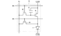
- FIG. 2 is a circuit diagram of a pixel circuit of the display device shown in FIG. 1.
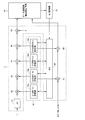
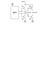
- FIG. 2 is a circuit diagram of a scanning line driving circuit of the display device shown in FIG. 1.
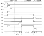
- 3 is a timing chart illustrating an operation of the display device illustrated in FIG. 1. It is a detailed timing chart of the display apparatus shown in FIG.
- FIG. 12 is a circuit diagram of a pixel circuit of the display device shown in FIG. 11.
- FIG. 12 is a circuit diagram of a scanning line driving circuit of the display device shown in FIG. 11. It is a detailed timing chart of the display apparatus shown in FIG. It is a block diagram which shows the structure of the display apparatus which concerns on the 3rd Embodiment of this invention.
- FIG. 16 is a circuit diagram of a pixel circuit of the display device shown in FIG. 15. It is a detailed timing chart of the display apparatus shown in FIG.
- FIG. 16 is a block diagram showing details of a correction data storage unit and a correction calculation unit in the display device shown in FIG.
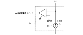
- FIG. 21 is a block diagram showing details of a data line drive / voltage measurement circuit of the display device shown in FIG. 20.
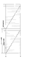
- FIG. 21 is a circuit diagram illustrating a configuration example of a voltage measurement unit of the data line drive / voltage measurement circuit illustrated in FIG. 20. It is a detailed timing chart of the display apparatus shown in FIG. It is a figure which shows the structure of the pulse output circuit contained in the conventional shift register. 6 is a timing chart of a display device having an extended line period.
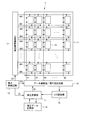
- FIG. 1 is a block diagram showing a configuration of a display device according to the first embodiment of the present invention.
- the display device 1 shown in FIG. 1 includes a display unit 11, a display control circuit 12, a scanning line driving circuit 13, a data line driving / current measuring circuit 14, an A / D converter 15, a correction data storage unit 16, and a correction calculation.
- This is an active matrix organic EL display device including a unit 17.
- m and n are integers of 2 or more
- i is an integer of 1 to n
- j is an integer of 1 to m.
- the display unit 11 includes 2n scanning lines GA1 to GAn, GB1 to GBn, m data lines S1 to Sm, and (m ⁇ n) pixel circuits 18.
- the scanning lines GA1 to GAn and GB1 to GBn are arranged in parallel to each other.
- the data lines S1 to Sm are arranged in parallel to each other and orthogonal to the scanning lines GA1 to GAn and GB1 to GBn.
- the scanning lines GA1 to GAn and the data lines S1 to Sm intersect at (m ⁇ n) locations.
- the (m ⁇ n) pixel circuits 18 are two-dimensionally arranged corresponding to the intersections of the scanning lines GA1 to GAn and the data lines S1 to Sm.
- the pixel circuit 18 is supplied with a high level power supply voltage ELVDD and a low level power supply voltage ELVSS using electrodes (not shown).
- ELVDD high level power supply voltage
- ELVSS low level power supply voltage
- the display control circuit 12 is a control circuit of the display device 1.
- the display control circuit 12 outputs a control signal CS1 to the scanning line drive circuit 13, outputs a control signal CS2 to the data line drive / current measurement circuit 14, and outputs a video signal X1 to the correction calculation unit 17.
- the control signal CS2 includes, for example, a source start pulse and a source clock. Details of the control signal CS1 will be described later.
- one frame period is divided into a video signal period and a vertical blanking period (see FIG. 4 described later).
- the video signal period includes n line periods (also called horizontal periods) corresponding to the n rows of pixel circuits 18.
- the scanning line driving circuit 13 drives the scanning lines GA1 to GAn and GB1 to GBn according to the control signal CS1. More specifically, the scanning line driving circuit 13 controls the voltage of the scanning line GAi to a high level (selection level) and the voltages of other scanning lines to a low level (non-selection level) in the i-th line period.
- the scanning line driving circuit 13 selects a pair of scanning lines GAi and GBi from the scanning lines GA1 to GAn and GB1 to GBn in the vertical blanking period, and applies a scanning signal to be described later to the scanning lines GAi and GBi.
- the voltages of other scanning lines are controlled to a low level.
- the scanning lines GAi and GBi selected in the vertical blanking period are switched every 4 frame periods.
- the data line drive / current measurement circuit 14 is supplied with the control signal CS2 and the corrected video signal X2 output from the correction calculation unit 17.
- the data line drive / current measurement circuit 14 is a data line drive circuit having a function of driving the data lines S1 to Sm and a function of measuring currents output from the pixel circuit 18 to the data lines S1 to Sm. More specifically, the data line drive / current measurement circuit 14 applies m voltages (hereinafter referred to as data voltages) corresponding to the video signal X2 to the data lines S1 to Sm in accordance with the control signal CS2 during the video signal period. To do.
- the data line drive / current measurement circuit 14 applies m measurement voltages to the data lines S1 to Sm according to the control signal CS2 during the vertical blanking period, and at that time, the pixel circuit 18 applies the data lines S1 to Sm.
- the output m currents are converted into voltages and output.
- the A / D converter 15 converts the output voltage of the data line drive / current measurement circuit 14 into digital data.
- the correction data storage unit 16 stores data necessary for correction calculation by the correction calculation unit 17 (hereinafter referred to as correction data).
- the correction calculation unit 17 updates the correction data stored in the correction data storage unit 16 based on the data output from the A / D converter 15 during the vertical blanking period.
- the correction calculation unit 17 refers to the correction data stored in the correction data storage unit 16, corrects the video signal X1 output from the display control circuit 12, and outputs the corrected video signal X2. To do.
- FIG. 2 is a circuit diagram of the pixel circuit 18 in the i-th row and j-th column.
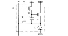
- the pixel circuit 18 includes an organic EL element L1, transistors Q1 to Q3, and a capacitor C1, and is connected to the scanning lines GAi and GBi and the data line Sj.
- the transistors Q1 to Q3 are N-channel TFTs (Thin Film Transistor).
- the high level power supply voltage ELVDD is applied to the drain terminal of the transistor Q1.
- the source terminal of the transistor Q1 is connected to the anode terminal of the organic EL element L1.
- a low level power supply voltage ELVSS is applied to the cathode terminal of the organic EL element L1.
- One conduction terminal left terminal in FIG.
- the transistor Q2 is connected to the data line Sj, and the other conduction terminal of the transistor Q2 is connected to the gate terminal of the transistor Q1.
- One conduction terminal (left terminal in FIG. 2) of the transistor Q3 is connected to the data line Sj, and the other conduction terminal of the transistor Q3 is connected to the source terminal of the transistor Q1 and the anode terminal of the organic EL element L1.
- the gate terminals of the transistors Q2 and Q3 are connected to the scanning lines GAi and GBi, respectively.
- the capacitor C1 is provided between the gate terminal and the drain terminal of the transistor Q1.
- the transistors Q1 to Q3 function as a drive transistor, a write control transistor, and a read control transistor, respectively.
- FIG. 3 is a circuit diagram of the scanning line driving circuit 13.
- the scanning line driving circuit 13 includes an n-stage shift register 41, n holding circuits 42, and n scanning signal output circuits 43.
- the control signal CS1 supplied to the scanning line driving circuit 13 includes a gate start pulse GSP, a gate clock GCK, a sampling signal SS, a clear signal CLR, a period designation signal PS, and timing signals TS1 and TS2.
- the i-th stage of the shift register 41, the i-th hold circuit 42, and the i-th scan signal output circuit 43 correspond to the scan lines GAi and GBi.
- the output of the i-th stage of the shift register 41 is referred to as a shift register output SRi
- the output of the i-th hold circuit 42 is referred to as a hold output HLDi.
- the gate start pulse GSP is given to the first stage of the shift register 41.
- the gate clock GCK is given to each stage of the shift register 41.
- the gate start pulse GSP becomes high level for a predetermined time before the start of the video signal period.
- the cycle of the gate clock GCK is one line period.
- the shift register 41 shifts the gate start pulse GSP according to the gate clock GCK. Therefore, the shift register outputs SR1 to SRn become high level in the order of SR1, SR2,. In the i-th line period, the shift register output SRi is at a high level, and the other shift register outputs are at a low level.
- the i-th hold circuit 42 receives the shift register output SRi, the sampling signal SS, and the clear signal CLR.
- the i-th hold circuit 42 holds the shift register output SRi in accordance with the sampling signal SS.
- the hold output HLDi is equal to the shift register output SRi while the sampling signal SS is at a high level, and does not change while the sampling signal SS is at a low level. However, when the clear signal CLR becomes high level, the hold output HLDi becomes low level.
- the i-th scanning signal output circuit 43 includes three AND gates 44, 46 and 47 and an OR gate 45.
- the AND gate 44 outputs a logical product of the hold output HLDi and the period specifying signal PS.
- the OR gate 45 outputs a logical sum of the shift register output SRi and the output of the AND gate 44.
- the AND gate 46 outputs a logical product of the timing signal TS1 and the output of the OR gate 45.
- the AND gate 47 outputs a logical product of the timing signal TS2 and the output of the AND gate 44.
- the output of the AND gate 46 is applied to the scanning line GAi, and the output of the AND gate 47 is applied to the scanning line GBi.
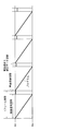
- FIG. 4 is a timing chart showing the operation of the display device 1.
- one frame period is divided into a video signal period and a vertical blanking period.
- n scanning lines GA1 to GAn are sequentially selected for each line period.
- the scanning line GAi is selected, and a data voltage is written in the m pixel circuits 18 connected to the scanning line GAi (described as a program in FIG. 4).
- the vertical blanking period a pair of scanning lines GAi and GBi is selected, and currents output to the data lines S1 to Sm from the m pixel circuits 18 connected to the scanning line GAi are measured. Based on the current measurement result, the correction data stored in the correction data storage unit 16 is updated (described as current measurement and correction data update in FIG. 4).
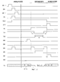
- FIG. 5 is a detailed timing chart of the display device 1.
- the scanning lines GA1 to GAn and GB1 to GBn can be driven according to the timing shown in FIG. 5 using the scanning line driving circuit 13 shown in FIG.
- a case where the scanning lines GAi and GBi are selected in the vertical blanking period will be described.
- the clear signal CLR becomes high level (active level) for a predetermined time after the end of the vertical blanking period, and becomes low level otherwise.
- the period designation signal PS is at a low level during the video signal period and is at a high level during the vertical blanking period. Since the vertical blanking period corresponds to a non-video signal period, the clear signal CLR becomes an active level after the end of the non-video signal period, and it can be said that the period designation signal PS indicates the video signal period or the non-video signal period. .
- the timing signal TS1 becomes a low level during a part of the vertical blanking period, and becomes a high level otherwise.
- the timing signal TS2 becomes a high level during a part of the period in which the timing signal TS1 is at a low level, and becomes a low level otherwise.
- a period in which the timing signal TS2 is at a high level is referred to as a period T2
- a period before the period T2 is after the periods T1 and T2.
- This period is referred to as period T3.
- the sampling signal SS becomes high level (active level) in the i-th line period in the previous video signal period, and becomes low level in other cases. .
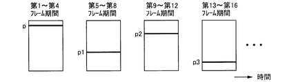
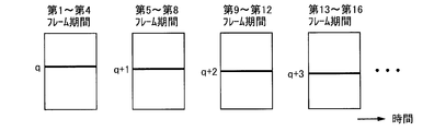
- the display control circuit 12 switches the line period for outputting the high level sampling signal SS every four frame periods.
- the outputs of the AND gates 44 and 47 are at a low level. Accordingly, in the video signal period, the voltages of the scanning lines GB1 to GBn are at a low level.
- the output of the AND gate 46 is equal to the shift register output SRi. As described above, in the i-th line period, the shift register output SRi is at a high level, and the other shift register outputs are at a low level. Accordingly, in the i-th line period, the voltage of the scanning line GAi is at a high level, and the voltages of the scanning lines GA1 to GAn (except for GAi) are at a low level.
- the shift register outputs SR1 to SRn are at low level at the start of the video signal period.
- the shift register output SRi becomes high level.
- the i-th hold circuit 42 receives the sampling signal SS when the shift register output SRi is at a high level. For this reason, the hold output HLDi is at a high level in the i-th and subsequent line periods.
- the other hold circuit 42 receives the sampling signal SS when the shift register output is at a low level. Therefore, the hold outputs HLD1 to HLDn (excluding HLDi) remain at a low level.
- the hold output HLDi becomes low level when the clear signal CLR next becomes high level.
- the period specifying signal PS and the hold output HLDi are at a high level, and the shift register outputs SR1 to SRn and the hold outputs HLD1 to HLDn (except for HLDi) are at a low level.
- the scanning signal output circuits 43 other than the i-th since the shift register output and the hold output are at the low level, the output of the AND gate 44 and the output of the OR gate 45 are at the low level. For this reason, the outputs of the AND gates 46 and 47 are at a low level regardless of the levels of the timing signals TS1 and TS2. Therefore, in the vertical blanking period, the voltages of the scanning lines GA1 to GAn and GB1 to GBn (excluding GAi and GBi) are at a low level.
- the voltage of the scanning line GAi is high in the periods T1 and T3, and is low in other periods, similarly to the voltage of the timing signal TS1. Similar to the voltage of the timing signal TS2, the voltage of the scanning line GBi is at a high level during the period T2, and is at a low level otherwise.
- TFT characteristics the characteristics of the transistor Q1
- OLED characteristics the characteristics of the organic EL element L1
- the voltage of the scanning line GAi is high level, and the voltage of the scanning line GBi is low level. Therefore, the transistor Q2 is turned on and the transistor Q3 is turned off.
- the data line drive / current measurement circuit 14 applies a data voltage Dij corresponding to the video signal X2 to the data line Sj. Therefore, the gate voltage of the transistor Q1 is Dij.
- the voltage of the scanning line GAi changes to a low level.
- the transistor Q2 is turned off.
- the gate voltage of the transistor Q1 is kept at Dij by the action of the capacitor C1.
- the transistor Q1 is turned on, and an amount of current corresponding to the gate-source voltage of the transistor Q1 flows through the organic EL element L1.
- the organic EL element L1 emits light with a luminance corresponding to the amount of flowing current. Accordingly, the organic EL element L1 emits light with a luminance corresponding to the data voltage Dij.
- the period T1 to T3 is set in the vertical blanking period.
- the voltage of the scanning line GAi is at a high level, and the voltage of the scanning line GBi is at a low level. Therefore, the transistor Q2 is turned on and the transistor Q3 is turned off.
- the data line drive / current measurement circuit 14 applies the measurement voltage Vmg (i, j) to the data line Sj. Therefore, the gate voltage of the transistor Q1 is Vmg (i, j).
- the measurement voltage Vmg (i, j) is either a TFT characteristic measurement voltage or an OLED characteristic measurement voltage.
- the transistor Q2 is turned off and the transistor Q3 is turned on.
- the transistor Q1 is turned on, and a current passing through the transistors Q1 and Q3 flows from the electrode having the high level power supply voltage ELVDD to the data line Sj.
- the OLED characteristic measurement voltage is applied in the period T1
- the transistor Q1 is turned off, and the current passing through the transistor Q3 and the organic EL element L1 from the data line Sj flows to the electrode having the low level power supply voltage ELVSS.
- the measurement voltage Vmg (i, j) is applied, the voltage of the data line Sj becomes Vm (i, j).
- the data line drive / current measurement circuit 14 measures the current flowing through the data line Sj in the period T2.
- the voltage of the scanning line GAi is at a high level, and the voltage of the scanning line GBi is at a low level.
- the data line drive / current measurement circuit 14 and the pixel circuit 18 operate in the same manner as in the i-th line period.
- the organic EL element L1 emits light with a luminance corresponding to the data voltage Dij.
- FIG. 6 is a block diagram showing details of the correction data storage unit 16 and the correction calculation unit 17.
- the correction data storage unit 16 includes a TFT gain storage unit 16a, an OLED gain storage unit 16b, a TFT offset storage unit 16c, and an OLED offset storage unit 16d.
- the four storage units 16a to 16d store (m ⁇ n) correction data corresponding to (m ⁇ n) pixel circuits 18, respectively.
- the TFT gain storage unit 16a stores a gain based on the detection result of the TFT characteristics (hereinafter referred to as TFT gain).
- the OLED gain storage unit 16b stores a gain based on the detection result of the OLED characteristic (hereinafter referred to as OLED gain).
- the TFT offset storage unit 16c stores an offset (hereinafter referred to as a TFT offset) based on the detection result of the TFT characteristics.
- the OLED offset storage unit 16d stores an offset based on the detection result of the OLED characteristic (hereinafter referred to as an OLED offset).
- the correction calculation unit 17 includes an LUT 61, multipliers 62, 63, 66 and 67, adders 64, 65 and 68, and a CPU 69.
- the correction calculation unit 17 receives the gradation P included in the video signal X1, the gradation P for detecting TFT characteristics, the value pre_Vmg_oled for detecting OLED characteristics, and the output of the A / D converter 15. From the four storage units 16a to 16d, correction data of the pixel circuit 18 in the i-th row and j-th column is read out.
- the LUT 61 performs gamma correction on the gradation P.
- the multiplier 62 multiplies the output of the LUT 61 by the TFT gain read from the TFT gain storage unit 16a.
- the multiplier 63 multiplies the output of the multiplier 62 by the OLED gain read from the OLED gain storage unit 16b.
- the adder 64 adds the TFT offset read from the TFT offset storage unit 16 c to the output of the multiplier 63.
- the adder 65 adds the OLED offset read from the OLED offset storage unit 16 d to the output of the adder 64.
- the multiplier 66 multiplies the output of the adder 65 by a coefficient Z for compensating for the attenuation of the data voltage.
- the correction calculation unit 17 outputs the video signal X2 including the output of the multiplier 66 to the data line drive / current measurement circuit 14 in the video signal period.
- the correction calculation unit 17 outputs the output of the multiplier 66 as data corresponding to the measurement voltage Vmg (i, j) to the data line drive / current measurement circuit 14 in the vertical blanking period in which the TFT characteristics are detected. .
- the multiplier 67 multiplies the value pre_Vmg_oled by the OLED gain read from the OLED gain storage unit 16b.
- the adder 68 adds the OLED offset read from the OLED offset storage unit 16 d to the output of the multiplier 67.
- the correction calculation unit 17 outputs the output of the adder 68 as data corresponding to the measurement voltage Vmg (i, j) to the data line drive / current measurement circuit 14 in the vertical blanking period in which the OLED characteristic is detected. .
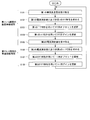
- FIG. 7 is a flowchart showing the operation of the CPU 69.
- the CPU 69 executes steps S101 to S116 shown in FIG. 7 every 4 frame periods.
- the CPU 69 executes steps S101 to S104 in the vertical blanking period of the first frame period, executes steps S105 to S108 in the vertical blanking period of the second frame period, and performs steps in the vertical blanking period of the third frame period.
- S109 to S112 are executed, and steps S113 to S116 are executed in the vertical blanking period of the fourth frame period.
- the data line drive / current measurement circuit 14 applies a first measurement voltage for measuring TFT characteristics to the data lines S1 to Sm in the period T1 of the vertical blanking period of the first frame period, and the pixel in the period T2.
- the current output from the circuit 18 to the data lines S1 to Sm is measured.
- the CPU 69 receives the first current measurement value obtained at this time from the A / D converter 15 (step S101).
- the CPU 69 obtains a first TFT characteristic based on the first current measurement value received in step S101 (step S102).
- the CPU 69 updates the TFT offset stored in the TFT offset storage unit 16c using the first TFT characteristics (step S103), and sets the TFT gain stored in the TFT gain storage unit 16a. Update (step S104).
- the data line drive / current measurement circuit 14 applies a second measurement voltage for measuring TFT characteristics to the data lines S1 to Sm in the vertical blanking period T1 of the second frame period, and the pixel in the period T2.
- the current output from the circuit 18 to the data lines S1 to Sm is measured.
- the CPU 69 receives the second current measurement value obtained at this time from the A / D converter 15 (step S105).
- the CPU 69 obtains a second TFT characteristic based on the second current measurement value received in step S105 (step S106).
- the CPU 69 updates the TFT offset stored in the TFT offset storage unit 16c using the second TFT characteristics (step S107), and sets the TFT gain stored in the TFT gain storage unit 16a. Update (step S108).
- the first measurement voltage and the second measurement voltage are different from each other.
- the first measurement voltage is a data voltage corresponding to a relatively low gradation
- the second measurement voltage is a data voltage corresponding to a relatively high gradation.
- the data line drive / current measurement circuit 14 applies a third measurement voltage for measuring OLED characteristics to the data lines S1 to Sm in the period T1 of the vertical blanking period of the third frame period, and the pixel in the period T2.
- the current output from the circuit 18 to the data lines S1 to Sm is measured.
- the CPU 69 receives the third current measurement value obtained at this time from the A / D converter 15 (step S109).
- the CPU 69 obtains a first OLED characteristic based on the third current measurement value received in step S109 (step S110).
- the CPU 69 updates the OLED offset stored in the OLED offset storage unit 16d by using the first OLED characteristic (step S111), and sets the OLED gain stored in the OLED gain storage unit 16b. Update (step S112).
- the data line drive / current measurement circuit 14 applies the fourth measurement voltage for measuring the OLED characteristics to the data lines S1 to Sm in the period T1 of the vertical blanking period of the fourth frame period, and the pixel in the period T2.
- the current output from the circuit 18 to the data lines S1 to Sm is measured.
- the CPU 69 receives the fourth current measurement value obtained at this time from the A / D converter 15 (step S113).
- the CPU 69 obtains a second OLED characteristic based on the fourth current measurement value received in step S113 (step S114).
- the CPU 69 updates the OLED offset stored in the OLED offset storage unit 16d using the second OLED characteristic (step S115), and sets the OLED gain stored in the OLED gain storage unit 16b. Update (step S116). Note that the third measurement voltage and the fourth measurement voltage are different from each other.
- the display control circuit 12 switches the line period for outputting the high level sampling signal SS every four frame periods. Therefore, the scanning line driving circuit 13 switches the scanning line selected in the vertical blanking period every four frame periods.
- the data line drive / current measurement circuit 14 measures the current output from the pixel circuit 18 to which the first to fourth measurement voltages are written in the first to fourth frame periods, respectively.
- the correction calculation unit 17 updates the correction data stored in the correction data storage unit 16 based on the first to fourth current measurement values in the first to fourth frame periods, respectively. In this way, by continuously selecting the same scanning line in the vertical blanking period, it is possible to switch the conditions for the same pixel circuit 18 and measure the current a plurality of times, and update the correction data based on the plurality of current measurement results. it can.
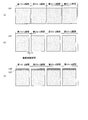
- FIGS. 8A to 8D are diagrams showing a method of selecting a scanning line selected in the vertical blanking period.
- the display control circuit 12 switches the line period for outputting the high-level sampling signal SS using, for example, the following first to fourth methods.
- the display control circuit 12 may switch the line period for outputting the high-level sampling signal SS in order (ascending order or descending order) every four frame periods.
- the scanning lines selected in the vertical blanking period are sequentially switched every 4 frame periods (see FIG. 8A).
- the current can be measured in order for each row of the pixel circuits 18 arranged in a two-dimensional manner, and the correction data can be updated based on the current measurement result.
- the display control circuit 12 may sequentially switch the line period for outputting the high-level sampling signal SS while skipping a predetermined number of line periods every four frame periods.
- the scanning lines selected in the vertical blanking period are sequentially switched while skipping a predetermined number of scanning lines every four frame periods (see FIG. 8B).
- the display control circuit 12 may randomly switch the line period for outputting the high-level sampling signal every four frame periods.
- the scanning line selected in the vertical blanking period is switched randomly every four frame periods (see FIG. 8C).
- the display control circuit 12 may switch the line period for outputting the high-level sampling signal while giving priority to the line period in a specific range every four frame periods.
- the scanning lines selected in the vertical blanking period are switched with priority given to scanning lines in a specific range every four frame periods (see FIG. 8D).
- the specific range for example, a range having a large influence on the image quality of the display image (for example, the central portion of the display screen) is selected.
- the pixel circuits 18 arranged in a two-dimensional manner by measuring the current for each row while giving priority to the pixel circuits in a specific range of rows, the pixel circuits having a large influence on the image quality of the display image are given priority. Current can be measured to improve the quality of the displayed image.
- the display device 1 is arranged two-dimensionally with 2n scanning lines GA1 to GAn, GB1 to GBn, and m data lines S1 to Sm (m ⁇ n).
- Display unit 11 including pixel circuits 18, scanning line driving circuit 13, data line driving circuit (data line driving / current measuring circuit 14), and video signal period or non-video signal period (vertical blanking period) And a display control circuit 12 that outputs a sampling signal SS that becomes high level (active level) in one line period within the video signal period.
- the scanning line driving circuit 13 is provided corresponding to the scanning line and the shift register 41 having n stages corresponding to the scanning line, and according to the sampling signal SS, the shift register output SRi (the corresponding stage of the shift register 41).
- N holding circuits 42 for holding output signals provided corresponding to the scanning lines, period designation signal PS, shift register output SRi, hold output HLDi (output signal of corresponding hold circuit 42), and timing signal TS1 , TS2, and n scanning signal output circuits 43 that output scanning signals to be applied to the corresponding scanning lines.
- the scanning signal output circuit 43 outputs a scanning signal for voltage writing when the shift register output SRi is at a high level (selection level) during the video signal period, and for current measurement when the hold output HLDi is at a high level during the vertical blanking period. And outputs a scanning signal for voltage writing.
- the scanning signal output circuit 43 outputs a shift register output SRi as a first scanning signal applied to the scanning line GAi (first scanning line) and applies it to the scanning line GBi (second scanning line) in the video signal period.
- a low level (non-selection level) signal is output as two scanning signals, and the hold output HLDi and timing signal TS1 (first timing signal) are high level (selection level) as the first scanning signal in the vertical blanking period.
- a signal that goes to a high level is output, and a signal that goes to a high level when the hold output HLDi and the timing signal TS2 (second timing signal) are at a high level are output as the second scanning signal.
- the timing signal TS1 is at a low level during a part of the vertical blanking period and is at a selection level at other times, and the timing signal TS2 is at a high level during a part of the period when the timing signal TS1 is at a low level. Otherwise, it is low level.
- the pixel circuit 18 includes an organic EL element L1 (electro-optical element), a transistor Q1 (drive transistor) provided in series with the organic EL element L1, and a data line Sj and a gate terminal (control terminal) of the transistor Q1. Provided between the data line Sj and the source terminal (one conduction terminal) of the transistor Q1 and having the gate terminal connected to the scanning line GAi and the scanning line GBi. It includes a transistor Q3 (reading control transistor) having a connected gate terminal, and a capacitor C1 provided between the gate terminal and drain terminal (the other conduction terminal) of the transistor Q1.
- the data line driving circuit measures the current output from the pixel circuit 18 when the measurement voltage is written to the pixel circuit 18.
- n hold circuits 42 hold the shift register outputs SR1 to SRn in a certain line period in the video signal period, one hold output is generated in the vertical blanking period in the non-video signal period.
- HLDi goes high.
- the scanning signal output circuit 43 outputs a scanning signal different from the video signal period in the vertical blanking period, so that the scanning lines GA1 to GAn are sequentially selected in the video signal period, and voltage writing is performed on the selected scanning line.
- a pair of scanning lines GAi and GBi are selected, and a current measuring and voltage writing scanning signal can be applied to the selected pair of scanning lines.
- a pair of scanning lines corresponding to the pixel circuits for one row is selected in the vertical blanking period, and the current (current output from the pixel circuit when the measurement voltage is written) for the pixel circuits for one row. Can be measured and voltage can be written.
- a simple circuit is used in a display device including a pixel circuit including an electro-optic element, three transistors, and a capacitor, and two types of scanning lines. A pair of scanning lines corresponding to one row of pixel circuits can be selected in the vertical blanking period, current can be measured for one row of pixel circuits, and voltage can be written.
- a scan line driver circuit is formed with a pixel circuit on a glass substrate (referred to as a gate driver monolithic structure)
- the area of a frame formed around the pixel region can be reduced.
- the display device 1 measures the current for the pixel circuits for one row during the vertical blanking period, the amount of line memory required for data transfer from the display control circuit 12 to the data line drive / current measurement circuit 14 is reduced. can do.
- the display control circuit 12 further outputs a clear signal CLR that becomes high level (active level) at the end of the vertical blanking period, and the hold outputs HLD1 to HLDn become low level according to the clear signal CLR. Therefore, by using the clear signal CLR, the hold outputs HLD1 to HLDn can be set to the low level at the end of the vertical blanking period.
- the display device 1 further includes a correction calculation unit 17 that corrects the video signal X1 based on the current measured by the data line drive / current measurement circuit 14. Therefore, by correcting the video signal X1 based on the current measurement result, it is possible to compensate for the decrease in luminance of the pixel and improve the image quality of the display image.
- the hold circuit 42 included in the scanning line driving circuit 13 is preferably formed using an oxide TFT having a small off-leakage current. Thereby, the shift register output SRi can be stably held over one frame period, and current measurement can be stably performed.
- the pixel circuit 18 is also preferably formed using an oxide TFT. Thereby, the transistor included in the hold circuit 42 and the transistor included in the pixel circuit 18 can be formed at the same time, and the manufacturing process can be shortened.
- a channel layer is formed of InGaZnOx (indium gallium zinc oxide) which is an oxide semiconductor mainly containing indium (In), gallium (Ga), zinc (Zn), and oxygen (O).
- the formed indium gallium zinc oxide-TFT can be used.
- an oxide TFT in which a channel layer is formed using an oxide semiconductor including two oxide semiconductors may be used. Even if such an oxide TFT is used, the same effect as indium gallium zinc oxide-TFT can be obtained.
- An oxide TFT such as an indium gallium zinc oxide TFT is effective when employed as an N-channel transistor included in a pixel circuit.
- the present invention does not exclude the use of a P-channel type oxide TFT.
- the oxide semiconductor layer included in the oxide TFT will be described.
- the oxide semiconductor layer is, for example, an In—Ga—Zn—O-based semiconductor layer.
- the oxide semiconductor layer includes, for example, an In—Ga—Zn—O-based semiconductor.
- An In—Ga—Zn—O-based semiconductor is a ternary oxide of indium, gallium, and zinc.
- a TFT having an In—Ga—Zn—O-based semiconductor layer has high mobility (more than 20 times that of an amorphous silicon TFT) and low leakage current (less than one hundredth of that of an amorphous silicon TFT). It is preferably used as a transistor in a pixel circuit. When a TFT having an In—Ga—Zn—O-based semiconductor layer is used, power consumption of the display device can be significantly reduced.
- the In—Ga—Zn—O-based semiconductor may be amorphous, may include a crystalline portion, and may have crystallinity.
- a crystalline In—Ga—Zn—O-based semiconductor in which the c-axis is oriented substantially perpendicular to the layer surface is preferable.
- Such a crystal structure of an In—Ga—Zn—O-based semiconductor is disclosed in, for example, Japanese Patent Application Laid-Open No. 2012-134475.
- the oxide semiconductor layer may include another oxide semiconductor instead of the In—Ga—Zn—O-based semiconductor.
- Zn—O based semiconductor ZnO
- In—Zn—O based semiconductor IZO (registered trademark)
- Zn—Ti—O based semiconductor ZTO
- Cd—Ge—O based semiconductor Cd—Pb—O based
- CdO cadmium oxide
- Mg—Zn—O based semiconductors In—Sn—Zn—O based semiconductors (eg, In 2 O 3 —SnO 2 —ZnO), In—Ga—Sn—O based semiconductors, etc. You may go out.
- FIG. 9 is a diagram for explaining a correction process in the display device according to the first modification.
- FIG. 9A shows the luminance of the organic EL element L1 in the pixel circuit 18 that is not selected in the vertical blanking period. In this case, the organic EL element L1 is in a non-light emitting state during a part of the vertical blanking period.
- FIG. 9B shows the luminance of the organic EL element L1 in the pixel circuit 18 selected in the vertical blanking period in the display device 1. In this case, the organic EL element L1 is in a non-light emitting state over the entire vertical blanking period over 4 frame periods.
- the average luminance of the organic EL element L1 in the pixel circuit 18 selected in the vertical blanking period is selected in the vertical blanking period.
- the average luminance of the organic EL element L1 in the pixel circuit 18 that is not set is lower for 4 frame periods.
- the data line voltage / voltage measurement circuit corrects the luminance decrease in the pixel circuit 18 as data. Apply to lines S1-Sm. Thereby, the luminance at the time of light emission of the organic EL element L1 in the pixel circuit 18 selected in the vertical blanking period is increased from LU1 to LU2, and the organic EL element L1 in the pixel circuit 18 selected in the vertical blanking period is increased. Is equal to the average luminance of the organic EL element L1 in the pixel circuit 18 that is not selected in the vertical blanking period. Therefore, according to the display device according to the first modification, by writing the corrected voltage to the pixel circuit that measures the current, the luminance reduction in the pixel circuit that measures the current is prevented and the image quality of the display image is prevented from being lowered. be able to.
- FIG. 10 is a circuit diagram of the scanning line driving circuit of the display device according to the second modification.
- the scanning line driving circuit 19 shown in FIG. 10 is obtained by adding 2n level shifters 48 to the scanning line driving circuit 13.
- Two level shifters 48 are provided corresponding to the scanning lines GAi and GBi.
- the input of one level shifter 48 is connected to the output of the AND gate 46, and the output is connected to the scanning line GAi.
- the other level shifter 48 has an input connected to the output of the AND gate 47 and an output connected to the scanning line GBi.
- the level shifter 48 is provided at the output stage of the scanning line driving circuit 19, so that the level of the output signal of the scanning signal output circuit 43 is driven to the scanning lines GA1 to GAn and GB1 to GBn. Can be converted to the required level.
- the display control circuit performs sampling at the end of the vertical blanking period instead of outputting the clear signal CLR that becomes high level at the end of the vertical blanking period to the scanning line driving circuit.
- the signal SS is set to high level.
- the output of the hold circuit 42 can be set to the low level at the end of the vertical blanking period.
- FIG. 11 is a block diagram showing a configuration of a display device according to the second embodiment of the present invention.
- a display device 2 shown in FIG. 11 is obtained by replacing the display unit 11 and the scanning line driving circuit 13 with a display unit 21 and a scanning line driving circuit 23, respectively, in the display device 1 according to the first embodiment.
- the same elements as those of the first embodiment are denoted by the same reference numerals and description thereof is omitted.
- the display unit 21 includes n scanning lines G1 to Gn, m data lines S1 to Sm, m monitor lines M1 to Mm, and (m ⁇ n) pixel circuits 28.
- the scanning lines G1 to Gn are arranged in parallel to each other.
- the data lines S1 to Sm and the monitor lines M1 to Mm are arranged in parallel to each other and orthogonal to the scanning lines G1 to Gn.
- the (m ⁇ n) pixel circuits 28 are two-dimensionally arranged corresponding to the intersections of the scanning lines G1 to Gn and the data lines S1 to Sm.
- FIG. 12 is a circuit diagram of the pixel circuit 28 in the i-th row and the j-th column.
- the pixel circuit 28 includes an organic EL element L1, transistors Q1 to Q3, and a capacitor C1, and is connected to the scanning line Gi, the data line Sj, and the monitor line Mj.
- the configuration of the pixel circuit 28 is the same as that of the pixel circuit 18 except for the following points.
- One conduction terminal (left terminal in FIG. 12) of the transistor Q3 is connected to the monitor line Mj.
- the gate terminals of the transistors Q2 and Q3 are connected to the scanning line Gi.
- the capacitor C1 is provided between the gate terminal and the source terminal of the transistor Q1.
- FIG. 13 is a circuit diagram of the scanning line driving circuit 23.
- the scanning line driving circuit 23 includes an n-stage shift register 41, n holding circuits 42, and n scanning signal output circuits 53.
- the control signal CS1 supplied to the scanning line driving circuit 23 includes a gate start pulse GSP, a gate clock GCK, a sampling signal SS, a clear signal CLR, and a period designation signal PS.
- the shift register 41 and the n hold circuits 42 operate in the same manner as in the first embodiment.
- the i-th scanning signal output circuit 53 includes an AND gate 54 and an OR gate 55.
- the AND gate 54 outputs a logical product of the hold output HLDi and the period specifying signal PS.
- the OR gate 55 outputs a logical sum of the shift register output SRi and the output of the AND gate 54.
- the output of the OR gate 55 is applied to the scanning line Gi.
- the display device 2 operates according to the timing chart shown in FIG. FIG. 14 is a detailed timing chart of the display device 2.
- the scanning lines G1 to Gn can be driven according to the timing shown in FIG. 14 using the scanning line driving circuit 23 shown in FIG.
- a case where the scanning line Gi is selected in the vertical blanking period will be described.
- the sampling signal SS, the clear signal CLR, and the period designation signal PS change in the same manner as in the first embodiment.
- the output of the AND gate 54 becomes low level, and the output of the OR gate 55 becomes equal to the shift register output SRi. Therefore, in the i-th line period, the voltage of the scanning line Gi is at a high level, and the voltages of the scanning lines G1 to Gn (except for Gi) are at a low level.
- Shift register outputs SR1 to SRn are at a low level at the start of the video signal period.
- the hold output HLDi becomes high level.
- the hold outputs HLD1 to HLDn remain at a low level.
- the period specifying signal PS and the hold output HLDi are at a high level, and the shift register outputs SR1 to SRn and the hold outputs HLD1 to HLDn (except for HLDi) are at a low level.
- the scan signal output circuits 53 other than the i-th since the shift register output and the hold output are at the low level, the output of the AND gate 54 and the output of the OR gate 55 are at the low level. Accordingly, in the vertical blanking period, the voltages of the scanning lines G1 to Gn (except for Gi) are at a low level.
- the hold output HLDi and the period specifying signal PS are at a high level, so the outputs of the AND gate 54 and the OR gate 55 are at a high level. Therefore, in the vertical blanking period, the voltage of the scanning line Gi is at a high level.
- the transistors Q2 and Q3 are turned on.
- the data line drive / current measurement circuit 14 applies the data voltage Dij to the data line Sj. Therefore, the gate voltage of the transistor Q1 is Dij.
- the voltage of the scanning line Gi changes to a low level.
- the transistors Q2 and Q3 are turned off.
- the gate voltage of the transistor Q1 is kept at Dij by the action of the capacitor C1.
- the transistor Q1 is turned on, and an amount of current corresponding to the gate-source voltage of the transistor Q1 flows through the organic EL element L1.
- the organic EL element L1 emits light with a luminance corresponding to the amount of flowing current.
- the voltage of the scanning line Gi changes to a high level.
- the transistors Q2 and Q3 are turned on.
- the data line drive / current measurement circuit 14 applies the measurement voltage Vmg (i, j) to the data line Sj. Therefore, the gate voltage of the transistor Q1 is Vmg (i, j).
- the measurement voltage Vmg (i, j) is either a TFT characteristic measurement voltage or an OLED characteristic measurement voltage.
- the transistor Q1 When the OLED characteristic measurement voltage is applied, the transistor Q1 is turned off, and the current passing through the transistor Q3 and the organic EL element L1 from the monitor line Mj flows to the electrode having the low level power supply voltage ELVSS. While the measurement voltage Vmg (i, j) is applied to the data line Sj, the voltage of the monitor line Mj becomes Vm (i, j).
- the data line drive / current measurement circuit 14 measures the current flowing through the monitor line Mj in a period excluding the terminal portion of the vertical blanking period.
- the data line drive / current measurement circuit 14 applies the data voltage Dij to the data line Sj.
- the pixel circuit 28 operates in the same manner as in the i-th line period.
- the clear signal CLR changes to high level
- the period designation signal PS changes to low level.
- the voltage of the scanning line Gi becomes low level.
- the organic EL element L1 emits light with a luminance corresponding to the data voltage Dij.
- correction data storage unit 16 and the correction calculation unit 17 included in the display device 2 are the same as those in the first embodiment (see FIG. 6).
- the operation of the CPU 69 included in the correction calculation unit 17 is the same as that in the first embodiment (see FIG. 7).
- the display device 2 is two-dimensionally arranged with n scanning lines G1 to Gn, m data lines S1 to Sm, and m monitor lines M1 to Mm.
- a display unit 21 including (m ⁇ n) pixel circuits 28, a scanning line driving circuit 23, a data line driving circuit (data line driving / current measuring circuit 14), and a video signal period or a non-video signal period (
- a display control circuit 12 that outputs a period specifying signal PS indicating a vertical blanking period) and a sampling signal SS that becomes a high level in one line period in the video signal period.
- the scanning line driving circuit 23 includes a shift register 41 having n stages corresponding to the scanning lines, and n holding circuits 42 provided corresponding to the scanning lines and holding the shift register output SRi according to the sampling signal SS. And n scanning signal output circuits 53 that are provided corresponding to the scanning lines and that output scanning signals applied to the corresponding scanning lines based on the period designation signal PS, the shift register output SRi, and the hold output HLDi. Contains.
- the scanning signal output circuit 53 outputs a shift register output SRi as a scanning signal in the video signal period, and outputs a hold output HLDi as a scanning signal in the vertical blanking period.
- the pixel circuit 28 includes an organic EL element L1 (electro-optical element), a transistor Q1 (drive transistor) provided in series with the organic EL element L1, and a data line Sj and a gate terminal (control terminal) of the transistor Q1.
- an organic EL element L1 organic EL element
- transistor Q1 drive transistor
- Sj data line
- gate terminal control terminal
- It includes a transistor Q3 (reading control transistor) having a connected gate terminal, and a capacitor C1 provided between the gate terminal and the source terminal of the transistor Q1.
- the display device 2 in a display device including a pixel circuit including an electro-optic element, three transistors, and a capacitor, and a monitor line, a simple circuit is used in a vertical blanking period. A pair of scanning lines corresponding to one row of pixel circuits can be selected, a current can be measured for one row of pixel circuits, and a voltage can be written.
- the display device 2 according to the present embodiment can also be configured with first to third modifications.
- FIG. 15 is a block diagram showing a configuration of a display device according to the third embodiment of the present invention.
- the display device 3 illustrated in FIG. 15 includes the display unit 11, the scanning line driving circuit 13, the correction data storage unit 16, and the correction calculation unit 17 in the display device 1 according to the first embodiment.
- the scanning line drive circuit 23, the correction data storage unit 36, and the correction calculation unit 37 are replaced.
- the same elements as those of the first and second embodiments are denoted by the same reference numerals and description thereof is omitted.
- the display unit 31 includes n scanning lines G1 to Gn, m data lines S1 to Sm, and (m ⁇ n) pixel circuits 38.
- the scanning lines G1 to Gn are arranged in parallel to each other.
- the data lines S1 to Sm are arranged in parallel to each other and orthogonal to the scanning lines G1 to Gn.
- the (m ⁇ n) pixel circuits 38 are two-dimensionally arranged corresponding to the intersections of the scanning lines G1 to Gn and the data lines S1 to Sm.
- the pixel circuit 38 is supplied with a reference voltage Vref using a wiring (not shown).
- FIG. 16 is a circuit diagram of the pixel circuit 38 in the i-th row and j-th column.
- the pixel circuit 38 includes an organic EL element L1, transistors Q1 to Q3, and a capacitor C1, and is connected to the scanning line Gi and the data line Sj.
- the transistor Q1 and the organic EL element L1 are connected in the same manner as the pixel circuit 18.
- One conduction terminal (left terminal in FIG. 16) of the transistor Q2 is connected to the data line Sj, and the other conduction terminal of the transistor Q2 is connected to the source terminal of the transistor Q1 and the anode terminal of the organic EL element L1.
- the drain terminal of the transistor Q3 is connected to the wiring having the reference voltage Vref, and the source terminal of the transistor Q3 is connected to the gate terminal of the transistor Q1.
- the gate terminals of the transistors Q2 and Q3 are connected to the scanning line Gi.
- the capacitor C1 is provided between the gate terminal and the source terminal of the transistor Q1.
- the transistors Q1 to Q3 function as a drive transistor, a write control transistor, and a reference voltage application transistor, respectively.
- the display device 3 operates according to the timing chart shown in FIG.
- FIG. 17 is a detailed timing chart of the display device 3.
- the timing chart shown in FIG. 17 is obtained by deleting the voltage change of the monitor line Mj from the timing chart shown in FIG.
- the scanning lines G1 to Gn can be driven according to the timing shown in FIG. 17 using the scanning line driving circuit 23 shown in FIG.
- the display control circuit 12 switches the line period for outputting the high level sampling signal SS every two frame periods.
- the transistors Q2 and Q3 are turned on.
- the data line drive / current measurement circuit 14 applies the data voltage Dij to the data line Sj. Therefore, the gate-source voltage of the transistor Q1 is (Vref-Dij).
- the voltage of the scanning line Gi changes to a low level.
- the transistors Q2 and Q3 are turned off.
- the gate-source voltage of the transistor Q1 is maintained at (Vref ⁇ Dij) by the action of the capacitor C1.
- the transistor Q1 is turned on, and a current corresponding to the gate-source voltage of the transistor Q1 flows through the organic EL element L1.
- the organic EL element L1 emits light with a luminance corresponding to the amount of flowing current.
- the voltage of the scanning line Gi changes to a high level.
- the transistors Q2 and Q3 are turned on.
- the data line drive / current measurement circuit 14 applies the measurement voltage Vmg (i, j) to the data line Sj. Therefore, the gate-source voltage of the transistor Q1 is ⁇ Vref ⁇ Vmg (i, j) ⁇ .
- the transistor Q1 is turned on, and a current passing through the transistors Q1 and Q2 flows from the electrode having the high level power supply voltage ELVDD to the data line Sj.
- the data line drive / current measurement circuit 14 measures the current output to the data line Sj in a period excluding the terminal part of the vertical blanking period.
- the data line drive / current measurement circuit 14 applies the data voltage Dij to the data line Sj.
- the pixel circuit 38 operates in the same manner as in the i-th line period.
- the clear signal CLR changes to high level
- the period designation signal PS changes to low level.
- the voltage of the scanning line Gi becomes low level.
- the organic EL element L1 emits light with a luminance corresponding to the data voltage Dij.
- FIG. 18 is a block diagram showing details of the correction data storage unit 36 and the correction calculation unit 37.
- the correction data storage unit 36 includes a TFT gain storage unit 36a and a TFT offset storage unit 36b.
- the two storage units 36a and 36b store (m ⁇ n) correction data corresponding to (m ⁇ n) pixel circuits 38, respectively.
- the TFT gain storage unit 36a stores the TFT gain
- the TFT offset storage unit 36b stores the TFT offset.
- the correction calculation unit 37 includes an LUT 71, multipliers 72 and 74, an adder 73, and a CPU 75.
- the correction calculation unit 37 receives the gradation P included in the video signal X1, the gradation P for detecting TFT characteristics, and the output of the A / D converter 15.
- the correction data of the pixel circuit 38 in the i-th row and j-th column is read from the two storage units 36a and 36b.
- the LUT 71 performs gamma correction on the gradation P.
- the multiplier 72 multiplies the output of the LUT 71 by the TFT gain read from the TFT gain storage unit 36a.
- the adder 73 adds the TFT offset read from the TFT offset storage unit 36 b to the output of the multiplier 72.
- the multiplier 74 multiplies the output of the adder 73 by a coefficient Z for compensating for the attenuation of the data voltage.
- the correction calculation unit 37 outputs the video signal X2 including the output of the multiplier 74 to the data line drive / current measurement circuit 14 in the video signal period.
- the correction calculation unit 37 outputs the output of the multiplier 74 to the data line drive / current measurement circuit 14 as data corresponding to the measurement voltage Vmg (i, j) during the vertical blanking period.
- FIG. 19 is a flowchart showing the operation of the CPU 75.
- the CPU 75 executes steps S101 to S108 shown in FIG. 19 every two frame periods.
- the CPU 75 executes steps S101 to S104 in the vertical blanking period of the first frame period, and executes steps S105 to S108 in the vertical blanking period of the second frame period.
- steps S101 to S108 the TFT offset stored in the TFT offset storage unit 36b is updated in steps S103 and S107, and the TFT gain stored in the TFT gain storage unit 36a is updated in steps S104 and S108.
- the second embodiment is the same as the first embodiment.
- the display control circuit 12 switches the line period for outputting the high level sampling signal SS every two frame periods. Therefore, the scanning line driving circuit 23 switches the scanning line selected in the vertical blanking period every two frame periods.
- the data line drive / current measurement circuit 14 measures the current output from the pixel circuit 38 into which the first and second measurement voltages are written in the first and second frame periods, respectively.
- the correction calculation unit 37 updates the correction data stored in the correction data storage unit 36 based on the first and second current measurement values in the first and second frame periods, respectively.
- the display device 3 includes (m ⁇ n) pixel circuits arranged two-dimensionally with n scanning lines G1 to Gn and m data lines S1 to Sm. 38, a scanning line driving circuit 23, a data line driving circuit (data line driving / current measuring circuit 14), and a period indicating a video signal period or a non-video signal period (vertical blanking period).
- the display control circuit 12 outputs the designation signal PS and the sampling signal SS that becomes high level in one line period within the video signal period.
- the configuration of the scanning line driving circuit 23 is the same as that of the second embodiment.
- the pixel circuit 38 includes an organic EL element L1 (electro-optical element), a transistor Q1 (driving transistor) provided in series with the organic EL element L1, a data line Sj, and one conduction terminal (source terminal) of the transistor Q1.
- the transistor Q2 write control transistor
- It includes a transistor Q3 (reference voltage applying transistor) having a gate terminal connected to the line Gi, and a capacitor C1 provided between the gate terminal and the source terminal (one conduction terminal) of the transistor Q1.
- a vertical circuit is used using a simple circuit.
- a pair of scanning lines corresponding to one row of pixel circuits in a line period can be selected, current can be measured for one row of pixel circuits, and a voltage can be written.
- the display device 3 according to the present embodiment can also be configured with first to third modifications.
- the display device including the data line driving circuit having the function of measuring the current output from the pixel circuit when the measurement voltage is written in the pixel circuit has been described.
- a display device including a data line driving circuit having a function of measuring a voltage at a node in the pixel circuit when a measurement current is supplied to the pixel circuit will be described.
- FIG. 20 is a block diagram showing the configuration of the display device according to this embodiment.
- a display device 4 shown in FIG. 20 is obtained by replacing the data line drive / current measurement circuit 14 with a data line drive / voltage measurement circuit 81 in the display device 1 according to the first embodiment.
- the same elements as those of the first embodiment are denoted by the same reference numerals and description thereof is omitted.
- the data line drive / voltage measurement circuit 81 is a data line drive circuit having a function of driving the data lines S1 to Sm and a function of measuring a voltage at a node in the pixel circuit 18. More specifically, the data line driving / voltage measuring circuit 81 applies m data voltages corresponding to the video signal X2 to the data lines S1 to Sm in accordance with the control signal CS2 during the video signal period. In the vertical blanking period, the data line drive / voltage measurement circuit 81 applies a predetermined voltage to the data lines S1 to Sm in accordance with the control signal CS2, and then supplies a measurement current (constant current) to the data lines S1 to Sm. Measure the voltage of the data lines S1 to Sm. As a result, the data line drive / voltage measurement circuit 81 measures the voltage at a certain node in the pixel circuit 18 (a node where the source terminal of the transistor Q1 and the anode terminal of the organic EL element L1 are connected).
- FIG. 21 is a block diagram showing details of the data line drive / voltage measurement circuit 81.
- the data line drive / voltage measurement circuit 81 includes a switch 82, a data line drive unit 83, and a voltage measurement unit 84 corresponding to the data line Sj.
- the switch 82 connects either the data line drive unit 83 or the voltage measurement unit 84 to the data line Sj in accordance with the selection signal SC.
- FIG. 22 is a circuit diagram illustrating a configuration example of the voltage measuring unit 84.
- the voltage measurement unit 84 shown in FIG. 22 includes an amplifier 85 and a constant current source 86.
- a low level power supply voltage ELVSS is fixedly applied to one input terminal of the amplifier 85.
- the other input terminal of the amplifier 85 and the constant current source 86 are connected to the data line Sj via the switch 82.
- the constant current source 86 supplies a constant current I_FIX to the data line Sj.
- the amplifier 85 amplifies the voltage of the data line Sj and outputs the amplified voltage to the A / D converter 15.
- the display device 4 operates according to the timing chart shown in FIG. FIG. 23 is a detailed timing chart of the display device 4.
- the display device 4 and the display device 1 according to the first embodiment perform the same operation during the video signal period and perform different operations during the vertical blanking period.
- the operation of the pixel circuit 18 in the i-th row and the j-th column in the vertical blanking period shown in FIG. 23 will be described.
- the voltage of the scanning line GAi is high level, and the voltage of the scanning line GBi is low level. Therefore, the transistor Q2 is turned on and the transistor Q3 is turned off.
- the data line drive / voltage measurement circuit 81 applies the measurement voltage Vmg (i, j) to the data line Sj. Therefore, the gate voltage of the transistor Q1 is Vmg (i, j).
- the measurement voltage Vmg (i, j) is either a TFT characteristic measurement voltage or an OLED characteristic measurement voltage.
- the constant current I_FIX is supplied to the data line Sj.
- the constant current I_FIX flows from the pixel circuit 18 to the data line drive / voltage measurement circuit 81 when measuring the TFT characteristics, and flows in the reverse direction when measuring the OLED characteristics.
- the constant current I_FIX and the TFT characteristic measurement voltage Vmg (i, j) are such that the voltage at the anode terminal of the organic EL element L1 in the period T2 (that is, the voltage measured when measuring the TFT characteristics) is equal to or lower than the threshold voltage of the organic EL element L1. Is set to be For this reason, when the TFT characteristic measurement voltage is applied to the data line Sj in the period T1, the current flows from the electrode having the high-level power supply voltage ELVDD to the data line Sj via the transistors Q1 and Q3 in the period T2. At this time, no current flows through the organic EL element L1. Therefore, only the characteristics of the transistor Q1 can be measured by using the TFT characteristic measurement voltage.
- the constant current I_FIX and the OLED characteristic measurement voltage Vmg (i, j) are measured at the time of measuring the OLED characteristic measurement voltage Vmg (i, j) and the voltage of the source terminal of the transistor Q1 in the period T2. Is set to be equal to or lower than the threshold voltage of the transistor Q1. Therefore, when the OLED characteristic measurement voltage is applied to the data line Sj in the period T1, the current flows from the data line Sj to the electrode having the low level power supply voltage ELVSS via the transistor Q3 and the organic EL element L1 in the period T2. . At this time, the transistor Q1 is not turned on. Therefore, only the characteristic of the organic EL element L1 can be measured by using the OLED characteristic measurement voltage.
- the transistor Q3 is turned on, so that the voltage of the data line Sj is equal to the voltage at the node where the source terminal of the transistor Q1 and the anode terminal of the organic EL element L1 are connected.
- the data line drive / voltage measurement circuit 81 measures the voltage of the data line Sj in the period T2, thereby connecting the node in the pixel circuit 18 (the node where the source terminal of the transistor Q1 and the anode terminal of the organic EL element L1 are connected). ).
- the voltage of the scanning line GAi is at a high level, and the voltage of the scanning line GBi is at a low level.
- the data line drive / voltage measurement circuit 81 and the pixel circuit 18 operate in the same manner as in the i-th line period.
- the organic EL element L1 emits light with a luminance corresponding to the data voltage Dij.
- the pixel when the measurement current (constant current of the constant current source 86) is supplied to the display unit 11, the scanning line driving circuit 13, and the pixel circuit 18 is used.
- a data line driving circuit data line driving / voltage measuring circuit 81 having a function of measuring a voltage at a node in the circuit 18 (a node where the source terminal of the transistor Q1 and the anode terminal of the organic EL element L1 are connected);
- a display control circuit 12 The configurations of the display unit 11, the display control circuit 12, and the scanning line driving circuit 13 are the same as those in the first embodiment.
- the display device 4 that includes the scanning line driving circuit 13 and measures the voltage of the pixel circuit 18 as described above also has a simple circuit similar to the display device 1 that includes the scanning line driving circuit 13 and measures the current of the pixel circuit 18. Is used to select a scanning line corresponding to a pixel circuit for one row in the vertical blanking period, and a voltage (a node in the pixel circuit when a measurement current is supplied to the pixel circuit) is applied to the pixel circuit for one row. Voltage) can be measured.
- the scanning line driving circuit 13 and a data line driving circuit (data line driving / voltage measuring circuit 81) having a function of measuring the voltage of the pixel circuit 18 are provided, and a display having the same configuration as the display device 1 is provided.
- the apparatus 4 has been described.
- the scanning line driving circuit 23 and the data line driving circuit having a function of measuring the voltage of the pixel circuit 28 are provided.
- the circuit 38 may be provided with a data line driving circuit having a function of measuring a voltage, and a display device having the same configuration as the display device 3 may be configured.
- a scanning line corresponding to a pixel circuit for one row is selected in a vertical blanking period, and a current is supplied to the pixel circuit for one row. Or the voltage can be measured.
- the features of the display devices according to the first to fourth embodiments and these modified examples are arbitrarily combined as long as they do not contradict their properties, thereby forming a display device having the features of a plurality of embodiments or modified examples. be able to.
- a driving method of an active matrix display device having a display unit including a plurality of first scanning lines, a plurality of second scanning lines, a plurality of data lines, and a plurality of pixel circuits arranged two-dimensionally, Driving the scanning line using a scanning line driving circuit; Driving the data line and measuring a current or voltage for the pixel circuit; A period designation signal indicating whether it is a video signal period or a non-video signal period, a sampling signal that becomes active in one line period within the video signal period, and a non-selection level in part of the vertical blanking period, otherwise Outputting a first timing signal that becomes a selection level, and a second timing signal that becomes a selection level during a part of a period in which the first timing signal is at a non-selection level and becomes a non-selection level otherwise.
- the scanning line driving circuit includes: A shift register having a plurality of stages corresponding to the scanning lines; A plurality of hold circuits provided corresponding to the scanning lines and holding shift register outputs output from corresponding stages of the shift register according to the sampling signal; A scanning signal output provided corresponding to the scanning line and outputting a scanning signal applied to the corresponding scanning line based on at least the period designation signal and the hold output output from the hold circuit corresponding to the shift register output.
- Circuit and The pixel circuit includes: An electro-optic element; A drive transistor provided in series with the electro-optic element; A write control transistor provided between the data line and the control terminal of the drive transistor and having a control terminal connected to the first scan line; A read control transistor provided between the data line and one conduction terminal of the drive transistor and having a control terminal connected to the second scan line; A capacitor provided between the control terminal of the driving transistor and the other conduction terminal; In the video signal period, the step of driving the scan line outputs the shift register output as a first scan signal to be applied to the first scan line using the scan signal output circuit, and applies it to the second scan line.
- a write scanning signal is output when the shift register output is at the selection level.
- the scanning signal output circuit is used.
- the hold output and the first timing signal are at a selection level as the first scanning signal
- a signal that is at a selection level is output
- the hold output and the second timing signal are at a selection level as the second scanning signal
- the scanning signal for measurement and writing is output. It is characterized in.
- a driving method of an active matrix display device having a display unit including a plurality of scanning lines, a plurality of data lines, a plurality of monitor lines, and a plurality of pixel circuits arranged two-dimensionally, Driving the scanning line using a scanning line driving circuit; Driving the data line and measuring a current or voltage for the pixel circuit; Outputting a period specifying signal indicating whether the video signal period or the non-video signal period, and a sampling signal that becomes an active level in one line period within the video signal period,
- the scanning line driving circuit includes: A shift register having a plurality of stages corresponding to the scanning lines; A plurality of hold circuits provided corresponding to the scanning lines and holding shift register outputs output from corresponding stages of the shift register according to the sampling signal; A scanning signal output provided corresponding to the scanning line and outputting a scanning signal applied to the corresponding scanning line based on at least the period designation signal and the hold output output from the hold circuit corresponding to the shift register output.
- the Circuit and The pixel circuit includes: An electro-optic element; A drive transistor provided in series with the electro-optic element; A write control transistor provided between the data line and a control terminal of the drive transistor and having a control terminal connected to the scan line; A read control transistor provided between the monitor line and one conduction terminal of the drive transistor and having a control terminal connected to the scan line; A capacitor provided between the control terminal of the driving transistor and one conduction terminal;
- the step of driving the scanning line outputs a scanning signal for writing when the shift register output is at a selected level by outputting the shift register output using the scanning signal output circuit during the video signal period.
- the scan signal output circuit is used to output the hold output, so that the scan signal for measurement and writing is output when the hold output is at a selected level.
- a driving method of an active matrix display device having a display unit including a plurality of scanning lines, a plurality of data lines, and a plurality of pixel circuits arranged two-dimensionally, Driving the scanning line using a scanning line driving circuit; Driving the data line and measuring a current or voltage for the pixel circuit; Outputting a period specifying signal indicating whether the video signal period or the non-video signal period, and a sampling signal that becomes an active level in one line period within the video signal period,
- the scanning line driving circuit includes: A shift register having a plurality of stages corresponding to the scanning lines; A plurality of hold circuits provided corresponding to the scanning lines and holding shift register outputs output from corresponding stages of the shift register according to the sampling signal; A scanning signal output provided corresponding to the scanning line and outputting a scanning signal applied to the corresponding scanning line based on at least the period designation signal and the hold output output from the hold circuit corresponding to the shift register output.
- the Circuit and The pixel circuit includes: An electro-optic element; A drive transistor provided in series with the electro-optic element; A write control transistor provided between the data line and one conduction terminal of the drive transistor and having a control terminal connected to the scan line; A reference voltage applying transistor provided between a control terminal of the driving transistor and a wiring having a reference voltage, and having a control terminal connected to the scanning line; A capacitor provided between the control terminal of the driving transistor and one conduction terminal;
- the step of driving the scanning line outputs a scanning signal for writing when the shift register output is at a selected level by outputting the shift register output using the scanning signal output circuit during the video signal period.
- the scan signal output circuit is used to output the hold output, so that the scan signal for measurement and writing is output when the hold output is at a selected level.
- the display device and the driving method thereof according to the present invention have a feature that a single scanning line can be selected in a vertical blanking period and a current or voltage can be measured for one row of pixel circuits using a simple circuit.
- the present invention can be used for various active matrix display devices including electro-optical elements such as organic EL elements.
- Scan line drive circuit 14 ... Data line drive / current measurement circuit 16, 36 ... Correction data storage part 17, 37... Correction operation unit 18, 28, 38... Pixel circuit 41... Shift register 42... Hold circuit 43, 53 ..
- Scan signal output circuit 81 ... Data line drive / voltage measurement circuit G1 to Gn, GA1 to GAn, GB1 to GBn ... scanning line S1 to Sm ... data line M1 to Mm ... monitor line EN1, EN2, ENA1, ENA2, ENB1, ENB2 ... enable signal L1 ... organic EL element Q1-Q3 ... transistor C1 ... capacitor CLR ... clear signal PS ... period Designation signal SS ... Sampling signal TS1, TS2 ... Timing signal
Landscapes
- Engineering & Computer Science (AREA)
- Physics & Mathematics (AREA)
- Computer Hardware Design (AREA)
- General Physics & Mathematics (AREA)
- Theoretical Computer Science (AREA)
- Control Of Indicators Other Than Cathode Ray Tubes (AREA)
- Control Of El Displays (AREA)
- Electroluminescent Light Sources (AREA)
Abstract
Description
複数の走査線と複数のデータ線と2次元状に配置された複数の画素回路とを含む表示部と、
前記走査線を駆動する走査線駆動回路と、
前記データ線を駆動する機能と前記画素回路について電流または電圧を測定する機能とを有するデータ線駆動回路と、
映像信号期間か非映像信号期間かを示す期間指定信号と、映像信号期間内の1ライン期間でアクティブレベルになるサンプリング信号とを出力する表示制御回路とを備え、
前記走査線駆動回路は、
前記走査線に対応する複数の段を有するシフトレジスタと、
前記走査線に対応して設けられ、前記サンプリング信号に従い、前記シフトレジスタの対応する段から出力されたシフトレジスタ出力を保持する複数のホールド回路と、
前記走査線に対応して設けられ、少なくとも前記期間指定信号と前記シフトレジスタ出力と対応するホールド回路から出力されたホールド出力とに基づき、対応する走査線に印加する走査信号を出力する走査信号出力回路とを含むことを特徴とする。
前記走査信号出力回路は、映像信号期間で前記シフトレジスタ出力が選択レベルのときには書き込み用の走査信号を出力し、非映像信号期間で前記ホールド出力が選択レベルのときには測定用および書き込み用の走査信号を出力することを特徴とする。
前記複数の走査線は、複数の第1走査線と複数の第2走査線とを含み、
前記表示制御回路は、第1タイミング信号と第2タイミング信号とをさらに出力し、
前記走査信号出力回路は、映像信号期間では、前記第1走査線に印加する第1走査信号として前記シフトレジスタ出力を出力し、前記第2走査線に印加する第2走査信号として非選択レベルの信号を出力し、非映像信号期間では、前記第1走査信号として前記ホールド出力と前記第1タイミング信号とに基づく信号を出力し、前記第2走査信号として前記ホールド出力と前記第2タイミング信号とに基づく信号を出力することを特徴とする。
前記画素回路は、
電気光学素子と、
前記電気光学素子と直列に設けられた駆動トランジスタと、
前記データ線と前記駆動トランジスタの制御端子との間に設けられ、前記第1走査線に接続された制御端子を有する書き込み制御トランジスタと、
前記データ線と前記駆動トランジスタの一方の導通端子との間に設けられ、前記第2走査線に接続された制御端子を有する読み出し制御トランジスタと、
前記駆動トランジスタの制御端子と他方の導通端子との間に設けられたコンデンサとを含むことを特徴とする。
前記第1タイミング信号は、非映像信号期間の一部で非選択レベルになり、それ以外では選択レベルになり、
前記第2タイミング信号は、前記第1タイミング信号が非選択レベルである期間の一部で選択レベルになり、それ以外では非選択レベルになり、
前記走査信号出力回路は、非映像信号期間では、前記第1走査信号として前記ホールド出力と前記第1タイミング信号が選択レベルのときに選択レベルになる信号を出力し、前記第2走査信号として前記ホールド出力と前記第2タイミング信号が選択レベルのときに選択レベルになる信号を出力することを特徴とする。
前記走査信号出力回路は、映像信号期間では前記走査信号として前記シフトレジスタ出力を出力し、非映像信号期間では前記走査信号として前記ホールド出力を出力することを特徴とする。
前記表示部は複数のモニタ線をさらに含み、
前記画素回路は、
電気光学素子と、
前記電気光学素子と直列に設けられた駆動トランジスタと、
前記データ線と前記駆動トランジスタの制御端子との間に設けられ、前記走査線に接続された制御端子を有する書き込み制御トランジスタと、
前記モニタ線と前記駆動トランジスタの一方の導通端子との間に設けられ、前記走査線に接続された制御端子を有する読み出し制御トランジスタと、
前記駆動トランジスタの制御端子と一方の導通端子との間に設けられたコンデンサとを含むことを特徴とする。
前記画素回路は、
電気光学素子と、
前記電気光学素子と直列に設けられた駆動トランジスタと、
前記データ線と前記駆動トランジスタの一方の導通端子との間に設けられ、前記走査線に接続された制御端子を有する書き込み制御トランジスタと、
前記駆動トランジスタの制御端子と基準電圧を有する配線との間に設けられ、前記走査線に接続された制御端子を有する基準電圧印加トランジスタと、
前記駆動トランジスタの制御端子と一方の導通端子との間に設けられたコンデンサとを含むことを特徴とする。
前記表示制御回路は、非映像信号期間の終了時にアクティブレベルになるクリア信号をさらに出力し、
前記ホールド回路の出力は、前記クリア信号に従い非選択レベルになることを特徴とする。
前記表示制御回路は、アクティブレベルのサンプリング信号を出力するライン期間を複数のフレーム期間ごとに切り替えることを特徴とする。
前記表示制御回路は、アクティブレベルのサンプリング信号を出力するライン期間を複数のフレーム期間ごとに順に切り替えることを特徴とする。
前記表示制御回路は、アクティブレベルのサンプリング信号を出力するライン期間を複数のフレーム期間ごとに所定数のライン期間を飛ばしながら順に切り替えることを特徴とする。
前記表示制御回路は、アクティブレベルのサンプリング信号を出力するライン期間を複数のフレーム期間ごとにランダムに切り替えることを特徴とする。
前記表示制御回路は、アクティブレベルのサンプリング信号を出力するライン期間を複数のフレーム期間ごとに特定範囲のライン期間を優先しながら切り替えることを特徴とする。
前記データ線駆動回路は、前記複数の画素回路のうち非映像信号期間で選択された画素回路に電圧を書き込むときには、前記画素回路における輝度低下分を補正した電圧を前記データ線に印加することを特徴とする。
前記データ線駆動回路で測定された電流または電圧に基づき、映像信号を補正する補正演算部をさらに備える。
前記データ線駆動回路は、前記画素回路に測定用電圧を書き込んだときに前記画素回路から出力された電流を測定することを特徴とする。
前記データ線駆動回路は、前記画素回路に測定用電流を流したときの前記画素回路内の節点の電圧を測定することを特徴とする。
走査線駆動回路を用いて前記走査線を駆動するステップと、
前記データ線を駆動し、前記画素回路について電流または電圧を測定するステップと、
映像信号期間か非映像信号期間かを示す期間指定信号と、映像信号期間内の1ライン期間でアクティブレベルになるサンプリング信号とを出力するステップとを備え、
前記走査線駆動回路は、
前記走査線に対応する複数の段を有するシフトレジスタと、
前記走査線に対応して設けられ、前記サンプリング信号に従い、前記シフトレジスタの対応する段から出力されたシフトレジスタ出力を保持する複数のホールド回路と、
前記走査線に対応して設けられ、少なくとも前記期間指定信号と前記シフトレジスタ出力と対応するホールド回路から出力されたホールド出力とに基づき、対応する走査線に印加する走査信号を出力する走査信号出力回路とを含むことを特徴とする。
図1は、本発明の第1の実施形態に係る表示装置の構成を示すブロック図である。図1に示す表示装置1は、表示部11、表示制御回路12、走査線駆動回路13、データ線駆動/電流測定回路14、A/D変換器15、補正データ記憶部16、および、補正演算部17を備えたアクティブマトリクス型の有機EL表示装置である。以下、mおよびnは2以上の整数、iは1以上n以下の整数、jは1以上m以下の整数であるとする。
図11は、本発明の第2の実施形態に係る表示装置の構成を示すブロック図である。図11に示す表示装置2は、第1の実施形態に係る表示装置1において、表示部11と走査線駆動回路13を、それぞれ、表示部21と走査線駆動回路23に置換したものである。本実施形態の構成要素のうち、第1の実施形態と同一の要素については、同一の参照符号を付して説明を省略する。
図15は、本発明の第3の実施形態に係る表示装置の構成を示すブロック図である。図15に示す表示装置3は、第1の実施形態に係る表示装置1において、表示部11、走査線駆動回路13、補正データ記憶部16、および、補正演算部17を、それぞれ、表示部31、走査線駆動回路23、補正データ記憶部36、および、補正演算部37に置換したものである。本実施形態の構成要素のうち、第1および第2の実施形態と同一の要素については、同一の参照符号を付して説明を省略する。
第1~第3の実施形態では、画素回路に測定用電圧を書き込んだときに画素回路から出力された電流を測定する機能を有するデータ線駆動回路を備えた表示装置について説明した。第4の実施形態では、画素回路に測定用電流を流したときの画素回路内の節点の電圧を測定する機能を有するデータ線駆動回路を備えた表示装置について説明する。
<第1の実施形態>
複数の第1走査線と複数の第2走査線と複数のデータ線と2次元状に配置された複数の画素回路とを含む表示部を有するアクティブマトリクス型の表示装置の駆動方法であって、
走査線駆動回路を用いて前記走査線を駆動するステップと、
前記データ線を駆動し、前記画素回路について電流または電圧を測定するステップと、
映像信号期間か非映像信号期間かを示す期間指定信号と、映像信号期間内の1ライン期間でアクティブレベルになるサンプリング信号と、垂直帰線期間の一部で非選択レベルになり、それ以外では選択レベルになる第1タイミング信号と、前記第1タイミング信号が非選択レベルである期間の一部で選択レベルになり、それ以外では非選択レベルになる第2タイミング信号とを出力するステップとを備え、
前記走査線駆動回路は、
前記走査線に対応する複数の段を有するシフトレジスタと、
前記走査線に対応して設けられ、前記サンプリング信号に従い、前記シフトレジスタの対応する段から出力されたシフトレジスタ出力を保持する複数のホールド回路と、
前記走査線に対応して設けられ、少なくとも前記期間指定信号と前記シフトレジスタ出力と対応するホールド回路から出力されたホールド出力とに基づき、対応する走査線に印加する走査信号を出力する走査信号出力回路とを含み、
前記画素回路は、
電気光学素子と、
前記電気光学素子と直列に設けられた駆動トランジスタと、
前記データ線と前記駆動トランジスタの制御端子との間に設けられ、前記第1走査線に接続された制御端子を有する書き込み制御トランジスタと、
前記データ線と前記駆動トランジスタの一方の導通端子との間に設けられ、前記第2走査線に接続された制御端子を有する読み出し制御トランジスタと、
前記駆動トランジスタの制御端子と他方の導通端子との間に設けられたコンデンサとを含み、
前記走査線を駆動するステップは、映像信号期間では、前記走査信号出力回路を用いて前記第1走査線に印加する第1走査信号として前記シフトレジスタ出力を出力し、前記第2走査線に印加する第2走査信号として非選択レベルの信号を出力することにより、前記シフトレジスタ出力が選択レベルのときに書き込み用の走査信号を出力し、非映像信号期間では、前記走査信号出力回路を用いて前記第1走査信号として前記ホールド出力と前記第1タイミング信号が選択レベルのときに選択レベルになる信号を出力し、前記第2走査信号として前記ホールド出力と前記第2タイミング信号が選択レベルのときに選択レベルになる信号を出力することにより、前記ホールド出力が選択レベルのときに測定用および書き込み用の走査信号を出力することを特徴とする。
複数の走査線と複数のデータ線と複数のモニタ線と2次元状に配置された複数の画素回路とを含む表示部を有するアクティブマトリクス型の表示装置の駆動方法であって、
走査線駆動回路を用いて前記走査線を駆動するステップと、
前記データ線を駆動し、前記画素回路について電流または電圧を測定するステップと、
映像信号期間か非映像信号期間かを示す期間指定信号と、映像信号期間内の1ライン期間でアクティブレベルになるサンプリング信号とを出力するステップとを備え、
前記走査線駆動回路は、
前記走査線に対応する複数の段を有するシフトレジスタと、
前記走査線に対応して設けられ、前記サンプリング信号に従い、前記シフトレジスタの対応する段から出力されたシフトレジスタ出力を保持する複数のホールド回路と、
前記走査線に対応して設けられ、少なくとも前記期間指定信号と前記シフトレジスタ出力と対応するホールド回路から出力されたホールド出力とに基づき、対応する走査線に印加する走査信号を出力する走査信号出力回路とを含み、
前記画素回路は、
電気光学素子と、
前記電気光学素子と直列に設けられた駆動トランジスタと、
前記データ線と前記駆動トランジスタの制御端子との間に設けられ、前記走査線に接続された制御端子を有する書き込み制御トランジスタと、
前記モニタ線と前記駆動トランジスタの一方の導通端子との間に設けられ、前記走査線に接続された制御端子を有する読み出し制御トランジスタと、
前記駆動トランジスタの制御端子と一方の導通端子との間に設けられたコンデンサとを含み、
前記走査線を駆動するステップは、映像信号期間では、前記走査信号出力回路を用いて前記シフトレジスタ出力を出力することにより、前記シフトレジスタ出力が選択レベルのときに書き込み用の走査信号を出力し、非映像信号期間では、前記走査信号出力回路を用いて前記ホールド出力を出力することにより、前記ホールド出力が選択レベルのときに測定用および書き込み用の走査信号を出力することを特徴とする。
複数の走査線と複数のデータ線と2次元状に配置された複数の画素回路とを含む表示部を有するアクティブマトリクス型の表示装置の駆動方法であって、
走査線駆動回路を用いて前記走査線を駆動するステップと、
前記データ線を駆動し、前記画素回路について電流または電圧を測定するステップと、
映像信号期間か非映像信号期間かを示す期間指定信号と、映像信号期間内の1ライン期間でアクティブレベルになるサンプリング信号とを出力するステップとを備え、
前記走査線駆動回路は、
前記走査線に対応する複数の段を有するシフトレジスタと、
前記走査線に対応して設けられ、前記サンプリング信号に従い、前記シフトレジスタの対応する段から出力されたシフトレジスタ出力を保持する複数のホールド回路と、
前記走査線に対応して設けられ、少なくとも前記期間指定信号と前記シフトレジスタ出力と対応するホールド回路から出力されたホールド出力とに基づき、対応する走査線に印加する走査信号を出力する走査信号出力回路とを含み、
前記画素回路は、
電気光学素子と、
前記電気光学素子と直列に設けられた駆動トランジスタと、
前記データ線と前記駆動トランジスタの一方の導通端子との間に設けられ、前記走査線に接続された制御端子を有する書き込み制御トランジスタと、
前記駆動トランジスタの制御端子と基準電圧を有する配線との間に設けられ、前記走査線に接続された制御端子を有する基準電圧印加トランジスタと、
前記駆動トランジスタの制御端子と一方の導通端子との間に設けられたコンデンサとを含み、
前記走査線を駆動するステップは、映像信号期間では、前記走査信号出力回路を用いて前記シフトレジスタ出力を出力することにより、前記シフトレジスタ出力が選択レベルのときに書き込み用の走査信号を出力し、非映像信号期間では、前記走査信号出力回路を用いて前記ホールド出力を出力することにより、前記ホールド出力が選択レベルのときに測定用および書き込み用の走査信号を出力することを特徴とする。
11、21、31…表示部
12…表示制御回路
13、19、23…走査線駆動回路
14…データ線駆動/電流測定回路
16、36…補正データ記憶部
17、37…補正演算部
18、28、38…画素回路
41…シフトレジスタ
42…ホールド回路
43、53…走査信号出力回路
81…データ線駆動/電圧測定回路
G1~Gn、GA1~GAn、GB1~GBn…走査線
S1~Sm…データ線
M1~Mm…モニタ線
EN1、EN2、ENA1、ENA2、ENB1、ENB2…イネーブル信号
L1…有機EL素子
Q1~Q3…トランジスタ
C1…コンデンサ
CLR…クリア信号
PS…期間指定信号
SS…サンプリング信号
TS1、TS2…タイミング信号
Claims (19)
- アクティブマトリクス型の表示装置であって、
複数の走査線と複数のデータ線と2次元状に配置された複数の画素回路とを含む表示部と、
前記走査線を駆動する走査線駆動回路と、
前記データ線を駆動する機能と前記画素回路について電流または電圧を測定する機能とを有するデータ線駆動回路と、
映像信号期間か非映像信号期間かを示す期間指定信号と、映像信号期間内の1ライン期間でアクティブレベルになるサンプリング信号とを出力する表示制御回路とを備え、
前記走査線駆動回路は、
前記走査線に対応する複数の段を有するシフトレジスタと、
前記走査線に対応して設けられ、前記サンプリング信号に従い、前記シフトレジスタの対応する段から出力されたシフトレジスタ出力を保持する複数のホールド回路と、
前記走査線に対応して設けられ、少なくとも前記期間指定信号と前記シフトレジスタ出力と対応するホールド回路から出力されたホールド出力とに基づき、対応する走査線に印加する走査信号を出力する走査信号出力回路とを含むことを特徴とする、表示装置。 - 前記走査信号出力回路は、映像信号期間で前記シフトレジスタ出力が選択レベルのときには書き込み用の走査信号を出力し、非映像信号期間で前記ホールド出力が選択レベルのときには測定用および書き込み用の走査信号を出力することを特徴とする、請求項1に記載の表示装置。
- 前記複数の走査線は、複数の第1走査線と複数の第2走査線とを含み、
前記表示制御回路は、第1タイミング信号と第2タイミング信号とをさらに出力し、
前記走査信号出力回路は、映像信号期間では、前記第1走査線に印加する第1走査信号として前記シフトレジスタ出力を出力し、前記第2走査線に印加する第2走査信号として非選択レベルの信号を出力し、非映像信号期間では、前記第1走査信号として前記ホールド出力と前記第1タイミング信号とに基づく信号を出力し、前記第2走査信号として前記ホールド出力と前記第2タイミング信号とに基づく信号を出力することを特徴とする、請求項2に記載の表示装置。 - 前記画素回路は、
電気光学素子と、
前記電気光学素子と直列に設けられた駆動トランジスタと、
前記データ線と前記駆動トランジスタの制御端子との間に設けられ、前記第1走査線に接続された制御端子を有する書き込み制御トランジスタと、
前記データ線と前記駆動トランジスタの一方の導通端子との間に設けられ、前記第2走査線に接続された制御端子を有する読み出し制御トランジスタと、
前記駆動トランジスタの制御端子と他方の導通端子との間に設けられたコンデンサとを含むことを特徴とする、請求項3に記載の表示装置。 - 前記第1タイミング信号は、非映像信号期間の一部で非選択レベルになり、それ以外では選択レベルになり、
前記第2タイミング信号は、前記第1タイミング信号が非選択レベルである期間の一部で選択レベルになり、それ以外では非選択レベルになり、
前記走査信号出力回路は、非映像信号期間では、前記第1走査信号として前記ホールド出力と前記第1タイミング信号が選択レベルのときに選択レベルになる信号を出力し、前記第2走査信号として前記ホールド出力と前記第2タイミング信号が選択レベルのときに選択レベルになる信号を出力することを特徴とする、請求項4に記載の表示装置。 - 前記走査信号出力回路は、映像信号期間では前記走査信号として前記シフトレジスタ出力を出力し、非映像信号期間では前記走査信号として前記ホールド出力を出力することを特徴とする、請求項2に記載の表示装置。
- 前記表示部は複数のモニタ線をさらに含み、
前記画素回路は、
電気光学素子と、
前記電気光学素子と直列に設けられた駆動トランジスタと、
前記データ線と前記駆動トランジスタの制御端子との間に設けられ、前記走査線に接続された制御端子を有する書き込み制御トランジスタと、
前記モニタ線と前記駆動トランジスタの一方の導通端子との間に設けられ、前記走査線に接続された制御端子を有する読み出し制御トランジスタと、
前記駆動トランジスタの制御端子と一方の導通端子との間に設けられたコンデンサとを含むことを特徴とする、請求項6に記載の表示装置。 - 前記画素回路は、
電気光学素子と、
前記電気光学素子と直列に設けられた駆動トランジスタと、
前記データ線と前記駆動トランジスタの一方の導通端子との間に設けられ、前記走査線に接続された制御端子を有する書き込み制御トランジスタと、
前記駆動トランジスタの制御端子と基準電圧を有する配線との間に設けられ、前記走査線に接続された制御端子を有する基準電圧印加トランジスタと、
前記駆動トランジスタの制御端子と一方の導通端子との間に設けられたコンデンサとを含むことを特徴とする、請求項6に記載の表示装置。 - 前記表示制御回路は、非映像信号期間の終了時にアクティブレベルになるクリア信号をさらに出力し、
前記ホールド回路の出力は、前記クリア信号に従い非選択レベルになることを特徴とする、請求項2に記載の表示装置。 - 前記表示制御回路は、アクティブレベルのサンプリング信号を出力するライン期間を複数のフレーム期間ごとに切り替えることを特徴とする、請求項2に記載の表示装置。
- 前記表示制御回路は、アクティブレベルのサンプリング信号を出力するライン期間を複数のフレーム期間ごとに順に切り替えることを特徴とする、請求項10に記載の表示装置。
- 前記表示制御回路は、アクティブレベルのサンプリング信号を出力するライン期間を複数のフレーム期間ごとに所定数のライン期間を飛ばしながら順に切り替えることを特徴とする、請求項10に記載の表示装置。
- 前記表示制御回路は、アクティブレベルのサンプリング信号を出力するライン期間を複数のフレーム期間ごとにランダムに切り替えることを特徴とする、請求項10に記載の表示装置。
- 前記表示制御回路は、アクティブレベルのサンプリング信号を出力するライン期間を複数のフレーム期間ごとに特定範囲のライン期間を優先しながら切り替えることを特徴とする、請求項10に記載の表示装置。
- 前記データ線駆動回路は、前記複数の画素回路のうち非映像信号期間で選択された画素回路に電圧を書き込むときには、前記画素回路における輝度低下分を補正した電圧を前記データ線に印加することを特徴とする、請求項2に記載の表示装置。
- 前記データ線駆動回路で測定された電流または電圧に基づき、映像信号を補正する補正演算部をさらに備えた、請求項2に記載の表示装置。
- 前記データ線駆動回路は、前記画素回路に測定用電圧を書き込んだときに前記画素回路から出力された電流を測定することを特徴とする、請求項2に記載の表示装置。
- 前記データ線駆動回路は、前記画素回路に測定用電流を流したときの前記画素回路内の節点の電圧を測定することを特徴とする、請求項2に記載の表示装置。
- 複数の走査線と複数のデータ線と2次元状に配置された複数の画素回路とを含む表示部を有するアクティブマトリクス型の表示装置の駆動方法であって、
走査線駆動回路を用いて前記走査線を駆動するステップと、
前記データ線を駆動し、前記画素回路について電流または電圧を測定するステップと、
映像信号期間か非映像信号期間かを示す期間指定信号と、映像信号期間内の1ライン期間でアクティブレベルになるサンプリング信号とを出力するステップとを備え、
前記走査線駆動回路は、
前記走査線に対応する複数の段を有するシフトレジスタと、
前記走査線に対応して設けられ、前記サンプリング信号に従い、前記シフトレジスタの対応する段から出力されたシフトレジスタ出力を保持する複数のホールド回路と、
前記走査線に対応して設けられ、少なくとも前記期間指定信号と前記シフトレジスタ出力と対応するホールド回路から出力されたホールド出力とに基づき、対応する走査線に印加する走査信号を出力する走査信号出力回路とを含むことを特徴とする、表示装置の駆動方法。
Priority Applications (4)
| Application Number | Priority Date | Filing Date | Title |
|---|---|---|---|
| JP2016529585A JP6109424B2 (ja) | 2014-06-23 | 2015-06-23 | 表示装置およびその駆動方法 |
| US15/321,340 US9792858B2 (en) | 2014-06-23 | 2015-06-23 | Display device and method for driving same |
| CN201580033854.2A CN106415701B (zh) | 2014-06-23 | 2015-06-23 | 显示装置及其驱动方法 |
| KR1020177000998A KR101748111B1 (ko) | 2014-06-23 | 2015-06-23 | 표시 장치 및 그 구동 방법 |
Applications Claiming Priority (2)
| Application Number | Priority Date | Filing Date | Title |
|---|---|---|---|
| JP2014128120 | 2014-06-23 | ||
| JP2014-128120 | 2014-06-23 |
Publications (1)
| Publication Number | Publication Date |
|---|---|
| WO2015199051A1 true WO2015199051A1 (ja) | 2015-12-30 |
Family
ID=54938133
Family Applications (1)
| Application Number | Title | Priority Date | Filing Date |
|---|---|---|---|
| PCT/JP2015/067964 Ceased WO2015199051A1 (ja) | 2014-06-23 | 2015-06-23 | 表示装置およびその駆動方法 |
Country Status (5)
| Country | Link |
|---|---|
| US (1) | US9792858B2 (ja) |
| JP (1) | JP6109424B2 (ja) |
| KR (1) | KR101748111B1 (ja) |
| CN (1) | CN106415701B (ja) |
| WO (1) | WO2015199051A1 (ja) |
Cited By (2)
| Publication number | Priority date | Publication date | Assignee | Title |
|---|---|---|---|---|
| WO2020202243A1 (ja) * | 2019-03-29 | 2020-10-08 | シャープ株式会社 | 表示装置およびその駆動方法 |
| JP2021532385A (ja) * | 2018-07-25 | 2021-11-25 | 京東方科技集團股▲ふん▼有限公司Boe Technology Group Co., Ltd. | シフトレジスタユニットおよびその駆動方法、ゲート駆動回路および表示装置 |
Families Citing this family (9)
| Publication number | Priority date | Publication date | Assignee | Title |
|---|---|---|---|---|
| JP2018054877A (ja) * | 2016-09-29 | 2018-04-05 | セイコーエプソン株式会社 | 電気光学装置、電気光学装置の制御方法および電子機器 |
| JP6781116B2 (ja) * | 2017-07-28 | 2020-11-04 | 株式会社Joled | 表示パネル、表示パネルの制御装置、および表示装置 |
| CN109935196B (zh) | 2018-02-14 | 2020-12-01 | 京东方科技集团股份有限公司 | 移位寄存器单元、栅极驱动电路、显示装置以及驱动方法 |
| CN109935197B (zh) | 2018-02-14 | 2021-02-26 | 京东方科技集团股份有限公司 | 移位寄存器单元、栅极驱动电路、显示装置以及驱动方法 |
| CN108877683A (zh) * | 2018-07-25 | 2018-11-23 | 京东方科技集团股份有限公司 | 栅极驱动电路及驱动方法、显示装置、阵列基板制造方法 |
| CN110520923B (zh) * | 2018-09-20 | 2022-05-13 | 京东方科技集团股份有限公司 | 具有时间共享信号线的像素电路、像素补偿方法和显示设备 |
| CN109166529B (zh) * | 2018-10-24 | 2020-07-24 | 合肥京东方卓印科技有限公司 | 显示面板、显示装置及驱动方法 |
| CN111028774B (zh) * | 2019-12-16 | 2021-07-06 | 深圳市华星光电半导体显示技术有限公司 | 显示面板及显示终端 |
| CN111445841B (zh) * | 2020-05-14 | 2022-04-08 | 京东方科技集团股份有限公司 | 显示装置及其检测方法 |
Citations (4)
| Publication number | Priority date | Publication date | Assignee | Title |
|---|---|---|---|---|
| WO2010001594A1 (ja) * | 2008-07-04 | 2010-01-07 | パナソニック株式会社 | 表示装置及びその制御方法 |
| WO2014174905A1 (ja) * | 2013-04-23 | 2014-10-30 | シャープ株式会社 | 表示装置およびその駆動電流検出方法 |
| WO2014203810A1 (ja) * | 2013-06-20 | 2014-12-24 | シャープ株式会社 | 表示装置およびその駆動方法 |
| WO2015037331A1 (ja) * | 2013-09-10 | 2015-03-19 | シャープ株式会社 | 表示装置およびその駆動方法 |
Family Cites Families (8)
| Publication number | Priority date | Publication date | Assignee | Title |
|---|---|---|---|---|
| JP4855648B2 (ja) | 2004-03-30 | 2012-01-18 | グローバル・オーエルイーディー・テクノロジー・リミテッド・ライアビリティ・カンパニー | 有機el表示装置 |
| BR112012010454A2 (pt) * | 2009-11-04 | 2016-03-08 | Sharp Kk | dispositivo de exibição de cristal líquido e método de acionamento do mesmo. |
| WO2011145666A1 (en) | 2010-05-21 | 2011-11-24 | Semiconductor Energy Laboratory Co., Ltd. | Pulse output circuit, shift register, and display device |
| CN103339715B (zh) | 2010-12-03 | 2016-01-13 | 株式会社半导体能源研究所 | 氧化物半导体膜以及半导体装置 |
| JP6138254B2 (ja) | 2013-06-27 | 2017-05-31 | シャープ株式会社 | 表示装置およびその駆動方法 |
| JP6116706B2 (ja) | 2013-12-19 | 2017-04-19 | シャープ株式会社 | 表示装置およびその駆動方法 |
| US10049620B2 (en) | 2014-04-23 | 2018-08-14 | Joled Inc. | Display device and method for controlling the same |
| WO2015190407A1 (ja) | 2014-06-10 | 2015-12-17 | シャープ株式会社 | 表示装置およびその駆動方法 |
-
2015
- 2015-06-23 KR KR1020177000998A patent/KR101748111B1/ko not_active Expired - Fee Related
- 2015-06-23 JP JP2016529585A patent/JP6109424B2/ja not_active Expired - Fee Related
- 2015-06-23 WO PCT/JP2015/067964 patent/WO2015199051A1/ja not_active Ceased
- 2015-06-23 US US15/321,340 patent/US9792858B2/en not_active Expired - Fee Related
- 2015-06-23 CN CN201580033854.2A patent/CN106415701B/zh active Active
Patent Citations (4)
| Publication number | Priority date | Publication date | Assignee | Title |
|---|---|---|---|---|
| WO2010001594A1 (ja) * | 2008-07-04 | 2010-01-07 | パナソニック株式会社 | 表示装置及びその制御方法 |
| WO2014174905A1 (ja) * | 2013-04-23 | 2014-10-30 | シャープ株式会社 | 表示装置およびその駆動電流検出方法 |
| WO2014203810A1 (ja) * | 2013-06-20 | 2014-12-24 | シャープ株式会社 | 表示装置およびその駆動方法 |
| WO2015037331A1 (ja) * | 2013-09-10 | 2015-03-19 | シャープ株式会社 | 表示装置およびその駆動方法 |
Cited By (3)
| Publication number | Priority date | Publication date | Assignee | Title |
|---|---|---|---|---|
| JP2021532385A (ja) * | 2018-07-25 | 2021-11-25 | 京東方科技集團股▲ふん▼有限公司Boe Technology Group Co., Ltd. | シフトレジスタユニットおよびその駆動方法、ゲート駆動回路および表示装置 |
| JP7366753B2 (ja) | 2018-07-25 | 2023-10-23 | 京東方科技集團股▲ふん▼有限公司 | シフトレジスタユニットおよびその駆動方法、ゲート駆動回路および表示装置 |
| WO2020202243A1 (ja) * | 2019-03-29 | 2020-10-08 | シャープ株式会社 | 表示装置およびその駆動方法 |
Also Published As
| Publication number | Publication date |
|---|---|
| KR101748111B1 (ko) | 2017-06-15 |
| JP6109424B2 (ja) | 2017-04-05 |
| US20170140703A1 (en) | 2017-05-18 |
| KR20170018420A (ko) | 2017-02-17 |
| CN106415701A (zh) | 2017-02-15 |
| CN106415701B (zh) | 2018-01-02 |
| JPWO2015199051A1 (ja) | 2017-04-20 |
| US9792858B2 (en) | 2017-10-17 |
Similar Documents
| Publication | Publication Date | Title |
|---|---|---|
| JP6109424B2 (ja) | 表示装置およびその駆動方法 | |
| CN105247603B (zh) | 显示装置及其驱动方法 | |
| US9711092B2 (en) | Display device and method for driving same | |
| JP6656265B2 (ja) | 表示装置およびその駆動方法 | |
| JP6129318B2 (ja) | 表示装置およびその駆動方法 | |
| US10062326B2 (en) | Display device and method for driving same | |
| JP5209905B2 (ja) | 有機発光ダイオード表示装置の駆動方法 | |
| US10614757B2 (en) | Flexible display device and method for detecting bending state thereof | |
| JP5015267B2 (ja) | 表示装置およびその製造方法 | |
| WO2014208458A1 (ja) | 表示装置およびその駆動方法 | |
| WO2015093097A1 (ja) | 表示装置およびその駆動方法 | |
| US11257430B2 (en) | Drive method and display device | |
| US20080231566A1 (en) | Minimizing dark current in oled display using modified gamma network | |
| US20230162681A1 (en) | Display, method, and 5t1c n-type pixel circuit | |
| JP2008134611A (ja) | 画像表示装置の駆動方法および画像表示装置 | |
| JP3988793B2 (ja) | アクティブマトリクス型表示装置の駆動方法およびアクティブマトリクス型表示装置 | |
| JP4915194B2 (ja) | 表示装置 |
Legal Events
| Date | Code | Title | Description |
|---|---|---|---|
| 121 | Ep: the epo has been informed by wipo that ep was designated in this application |
Ref document number: 15811771 Country of ref document: EP Kind code of ref document: A1 |
|
| ENP | Entry into the national phase |
Ref document number: 2016529585 Country of ref document: JP Kind code of ref document: A |
|
| WWE | Wipo information: entry into national phase |
Ref document number: 15321340 Country of ref document: US |
|
| NENP | Non-entry into the national phase |
Ref country code: DE |
|
| ENP | Entry into the national phase |
Ref document number: 20177000998 Country of ref document: KR Kind code of ref document: A |
|
| 122 | Ep: pct application non-entry in european phase |
Ref document number: 15811771 Country of ref document: EP Kind code of ref document: A1 |