WO2015198447A1 - 無停電電源装置 - Google Patents
無停電電源装置 Download PDFInfo
- Publication number
- WO2015198447A1 WO2015198447A1 PCT/JP2014/066987 JP2014066987W WO2015198447A1 WO 2015198447 A1 WO2015198447 A1 WO 2015198447A1 JP 2014066987 W JP2014066987 W JP 2014066987W WO 2015198447 A1 WO2015198447 A1 WO 2015198447A1
- Authority
- WO
- WIPO (PCT)
- Prior art keywords
- power
- power supply
- inverter
- bypass
- control unit
- Prior art date
- Legal status (The legal status is an assumption and is not a legal conclusion. Google has not performed a legal analysis and makes no representation as to the accuracy of the status listed.)
- Ceased
Links
Images








Classifications
-
- H—ELECTRICITY
- H02—GENERATION; CONVERSION OR DISTRIBUTION OF ELECTRIC POWER
- H02J—ELECTRIC POWER NETWORKS; CIRCUIT ARRANGEMENTS OR SYSTEMS FOR SUPPLYING OR DISTRIBUTING ELECTRIC POWER; SYSTEMS FOR STORING ELECTRIC ENERGY
- H02J9/00—Circuit arrangements for emergency or stand-by power supply, e.g. for emergency lighting
- H02J9/04—Circuit arrangements for emergency or stand-by power supply, e.g. for emergency lighting in which the distribution system is disconnected from the normal source and connected to a standby source
- H02J9/06—Circuit arrangements for emergency or stand-by power supply, e.g. for emergency lighting in which the distribution system is disconnected from the normal source and connected to a standby source with automatic change-over, e.g. UPS systems
- H02J9/061—Circuit arrangements for emergency or stand-by power supply, e.g. for emergency lighting in which the distribution system is disconnected from the normal source and connected to a standby source with automatic change-over, e.g. UPS systems for DC powered loads
-
- H—ELECTRICITY
- H02—GENERATION; CONVERSION OR DISTRIBUTION OF ELECTRIC POWER
- H02J—ELECTRIC POWER NETWORKS; CIRCUIT ARRANGEMENTS OR SYSTEMS FOR SUPPLYING OR DISTRIBUTING ELECTRIC POWER; SYSTEMS FOR STORING ELECTRIC ENERGY
- H02J7/00—Circuit arrangements for charging or discharging batteries or for supplying loads from batteries
- H02J7/865—Battery or charger load switching, e.g. concurrent charging and load supply
-
- H—ELECTRICITY
- H02—GENERATION; CONVERSION OR DISTRIBUTION OF ELECTRIC POWER
- H02J—ELECTRIC POWER NETWORKS; CIRCUIT ARRANGEMENTS OR SYSTEMS FOR SUPPLYING OR DISTRIBUTING ELECTRIC POWER; SYSTEMS FOR STORING ELECTRIC ENERGY
- H02J9/00—Circuit arrangements for emergency or stand-by power supply, e.g. for emergency lighting
- H02J9/02—Circuit arrangements for emergency or stand-by power supply, e.g. for emergency lighting in which an auxiliary distribution system and its associated lamps are brought into service
-
- H—ELECTRICITY
- H02—GENERATION; CONVERSION OR DISTRIBUTION OF ELECTRIC POWER
- H02J—ELECTRIC POWER NETWORKS; CIRCUIT ARRANGEMENTS OR SYSTEMS FOR SUPPLYING OR DISTRIBUTING ELECTRIC POWER; SYSTEMS FOR STORING ELECTRIC ENERGY
- H02J9/00—Circuit arrangements for emergency or stand-by power supply, e.g. for emergency lighting
- H02J9/04—Circuit arrangements for emergency or stand-by power supply, e.g. for emergency lighting in which the distribution system is disconnected from the normal source and connected to a standby source
- H02J9/06—Circuit arrangements for emergency or stand-by power supply, e.g. for emergency lighting in which the distribution system is disconnected from the normal source and connected to a standby source with automatic change-over, e.g. UPS systems
- H02J9/066—Circuit arrangements for emergency or stand-by power supply, e.g. for emergency lighting in which the distribution system is disconnected from the normal source and connected to a standby source with automatic change-over, e.g. UPS systems characterised by the use of dynamo-electric machines
-
- Y—GENERAL TAGGING OF NEW TECHNOLOGICAL DEVELOPMENTS; GENERAL TAGGING OF CROSS-SECTIONAL TECHNOLOGIES SPANNING OVER SEVERAL SECTIONS OF THE IPC; TECHNICAL SUBJECTS COVERED BY FORMER USPC CROSS-REFERENCE ART COLLECTIONS [XRACs] AND DIGESTS
- Y02—TECHNOLOGIES OR APPLICATIONS FOR MITIGATION OR ADAPTATION AGAINST CLIMATE CHANGE
- Y02B—CLIMATE CHANGE MITIGATION TECHNOLOGIES RELATED TO BUILDINGS, e.g. HOUSING, HOUSE APPLIANCES OR RELATED END-USER APPLICATIONS
- Y02B70/00—Technologies for an efficient end-user side electric power management and consumption
- Y02B70/30—Systems integrating technologies related to power network operation and communication or information technologies for improving the carbon footprint of the management of residential or tertiary loads, i.e. smart grids as climate change mitigation technology in the buildings sector, including also the last stages of power distribution and the control, monitoring or operating management systems at local level
-
- Y—GENERAL TAGGING OF NEW TECHNOLOGICAL DEVELOPMENTS; GENERAL TAGGING OF CROSS-SECTIONAL TECHNOLOGIES SPANNING OVER SEVERAL SECTIONS OF THE IPC; TECHNICAL SUBJECTS COVERED BY FORMER USPC CROSS-REFERENCE ART COLLECTIONS [XRACs] AND DIGESTS
- Y04—INFORMATION OR COMMUNICATION TECHNOLOGIES HAVING AN IMPACT ON OTHER TECHNOLOGY AREAS
- Y04S—SYSTEMS INTEGRATING TECHNOLOGIES RELATED TO POWER NETWORK OPERATION, COMMUNICATION OR INFORMATION TECHNOLOGIES FOR IMPROVING THE ELECTRICAL POWER GENERATION, TRANSMISSION, DISTRIBUTION, MANAGEMENT OR USAGE, i.e. SMART GRIDS
- Y04S20/00—Management or operation of end-user stationary applications or the last stages of power distribution; Controlling, monitoring or operating thereof
- Y04S20/20—End-user application control systems
Definitions
- the present invention relates to an uninterruptible power supply, and more particularly to an uninterruptible power supply having an eco mode for supplying AC power to a load via a bypass switch.
- an uninterruptible power supply is a converter that converts AC power from an AC power source into DC power, and an inverter that converts DC power generated by the converter or DC power of a power storage device into AC power and supplies it to a load.
- a bypass switch including a thyristor switch and a contactor connected in parallel between the AC power source and the load, and a control device for controlling them.
- the converter and the inverter are used during normal times when the AC power is normally supplied from the AC power supply, and the power supply is continued with the inverter during a power failure when the supply of AC power from the AC power supply is stopped.
- Such a circuit method is always called an inverter power supply method.
- the constant inverter power supply system supplies power to the load through the inverter via the DC link when the AC power supply is normal or during a power failure, making it easy to ensure the output power quality regardless of the input power quality.
- the power feeding stability is excellent.
- power loss occurs because energy passes through the converter and the inverter at normal times, and improvement of the operation efficiency is a problem.
- the uninterruptible power supply apparatus normally performs bypass power feeding that supplies AC power to the load from the AC power source via the thyristor switch that is a bias switch.
- the power supply is switched from the bypass power supply to the inverter power supply that supplies AC power from the inverter to the load.
- the bypass switch When the bypass switch is configured by combining a thyristor switch and a contactor, the contactor is turned off later than the thyristor switch because the contactor response time is longer than the thyristor switch response time. For this reason, the degree of instantaneous voltage drop (instantaneous voltage drop time and voltage drop degree) increases, which may have a large effect on the load.
- the main object of the present invention is to provide an uninterruptible power supply capable of preventing the occurrence of an instantaneous voltage drop when switching from power supply in eco mode to supplying AC power to a load via a bypass switch to inverter power supply. It is to provide a power supply.
- the uninterruptible power supply according to the present invention is connected between an AC power supply and a bypass AC power supply and a load.
- the uninterruptible power supply is a DC terminal that receives AC power from an AC power source, a bypass terminal that receives AC power from a bypass AC power source, an output terminal that outputs AC power to a load, and AC power input to the input terminal.
- the bypass switch whose one terminal is connected to the output terminal, the first switch connected between the bypass terminal and the other terminal of the bypass switch, and the input terminal and the AC side terminal of the converter
- a second switch connected between the first node located and the other terminal of the bypass switch; an input terminal;
- a third switch connected between the first node, and a bypass switch, and a switch controller for controlling on and off of the third switch from the first.
- the uninterruptible power supply has a first operation mode for supplying AC power from the inverter to the load, and a second operation mode for supplying AC power to the load from the AC power supply or bypass AC power supply via the bypass switch. is doing.
- the uninterruptible power supply is configured to shift to the first operation mode when a power failure occurs when the supply of AC power from the AC power supply or bypass AC power supply is stopped when the second operation mode is selected. Is done.
- the switching control unit has a bypass switch, a second switch, a first switch, and a normal switch when the AC power is normally supplied from the AC power supply or the bypass AC power supply. While one of the third switches is turned on, the bypass switch is turned off during a power failure.
- the power conversion control unit causes the converter to perform reverse conversion, converts the DC power output from the power storage device into AC power, and outputs the AC power to the first node.
- the DC power output from the power storage device is converted into AC power after being converted into AC power and output to the output terminal, and the phase and magnitude of the AC voltage output to each of the first node and the output terminal Are controlled so as to be equal to each other.
- the bypass switch includes a contactor having one terminal connected to the output terminal and the other terminal connected to the first and second switches.
- the switching control unit turns on the bypass switch and the second and third switches, and turns off the first switch, thereby supplying the AC supplied from the AC power source. Supply power to the load.
- the power conversion control unit when the power conversion control unit turns off the bypass switch by the switching control unit, the AC voltage output to the AC side terminal of the converter is synchronized with the AC voltage supplied from the AC power supply before the power failure. Controls the reverse conversion in the converter.
- the power conversion control unit further controls reverse conversion in the inverter so that the AC voltage output to the output terminal is synchronized with the AC voltage supplied from the AC power supply before the power failure.
- the power conversion control unit is configured to generate a gate signal for controlling the inverter so that the AC voltage output to the output terminal is synchronized with the AC voltage supplied from the AC power supply.
- the power conversion control unit In the second operation mode, the power conversion control unit normally stops the output of the gate signal to place the inverter in a reverse conversion standby state while the switching control unit turns off the bypass switch. Outputs a gate signal.
- the uninterruptible power supply is configured to return to the second operation mode when a power recovery occurs in which the supply of AC power from the AC power supply resumes after shifting to the first operation mode.
- the power conversion control unit causes the converter to perform forward conversion in response to the detection of the power recovery of the AC power supply, and the AC voltage output to the output terminal is supplied from the AC power supply after the power recovery.
- the reverse conversion in the inverter is controlled so as to synchronize with.
- the switching control unit turns on the bypass switch when the AC voltage output to the output terminal is synchronized with the AC voltage supplied from the AC power supply after the power recovery.
- the switching control unit is supplied from the bypass AC power source by turning on the bypass switch and the first and second switches and turning off the third switch. Supply AC power to the load.
- the power conversion control unit when the power conversion control unit turns off the bypass switch by the switching control unit, the AC voltage output to the AC side terminal of the converter is synchronized with the AC voltage supplied from the bypass AC power supply before the power failure.
- the inverse conversion in the converter is controlled.
- the power conversion control unit further controls reverse conversion in the inverter so that the AC voltage output to the output terminal is synchronized with the AC voltage supplied from the bypass AC power supply before the power failure.
- the power conversion control unit is configured to generate a gate signal for controlling the inverter so that the AC voltage output to the output terminal is synchronized with the AC voltage supplied from the bypass AC power source. .
- the power conversion control unit In the second operation mode, the power conversion control unit normally stops the output of the gate signal to place the inverter in a reverse conversion standby state while the switching control unit turns off the bypass switch. Outputs a gate signal.
- the uninterruptible power supply is configured to return to the second operation mode when a recovery occurs in which the supply of AC power from the bypass AC power supply resumes after the transition to the first operation mode.
- the power conversion control unit causes the converter to perform forward conversion in response to detection of power recovery of the bypass AC power source, and AC voltage output to the output terminal is supplied from the bypass AC power source after power recovery.
- the reverse conversion in the inverter is controlled so as to be synchronized with the AC voltage.
- the switching control unit turns on the bypass switch when the AC voltage output to the output terminal is synchronized with the AC voltage supplied from the bypass AC power supply after the power recovery.
- the uninterruptible power supply further includes a reactor having one terminal connected to the input terminal and the other terminal connected to the AC side terminal of the converter.
- the first node is located between the other terminal of the reactor and the AC side terminal of the converter.
- the uninterruptible power supply further includes a reactor having one terminal connected to the input terminal and the other terminal connected to the AC side terminal of the converter.
- the first node is located between the input terminal and one terminal of the reactor.
- the uninterruptible power supply further includes a first transformer connected between the AC power supply and the input terminal, and a second transformer connected between the bypass AC power supply and the bypass terminal. .
- an instantaneous voltage drop is prevented from occurring when switching from power supply in the eco mode to inverter power supply. can do.
- the operation efficiency of the uninterruptible power supply can be improved while securing the power feeding stability to the load.
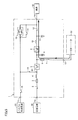
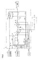
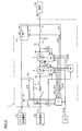
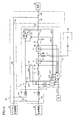
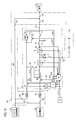
- Embodiment 1 is an overall configuration diagram of an uninterruptible power supply according to Embodiment 1 of the present invention. It is a figure for demonstrating the flow of the electric power in execution of eco mode. It is a figure for demonstrating the flow of electric power when the power failure of AC power supply is detected during execution of eco mode. It is a functional block diagram which shows the control structure for switching from electric power feeding in eco mode to inverter electric power feeding in the uninterruptible power supply concerning Embodiment 1 of the present invention. It is a figure for demonstrating the flow of the electric power during execution of inverter electric power feeding. It is a figure for demonstrating the flow of electric power when the power recovery of AC power supply is detected during execution of inverter electric power feeding.
- FIG. 1 is an overall configuration diagram of an uninterruptible power supply according to Embodiment 1 of the present invention.
- the uninterruptible power supply according to Embodiment 1 of the present invention is connected to AC power supply 50, bypass AC power supply 51 and load 52.
- AC power supply 50 and bypass AC power supply 51 are AC power supplies that supply AC power to the uninterruptible power supply.
- Each of these AC power sources is constituted by, for example, a commercial AC power source or a private generator.
- FIG. 1 and the drawings described hereinafter a three-phase three-wire system is shown as an example of an AC power supply. For simplification of the drawings and description, only a circuit for one phase is representatively shown in FIG.
- the type of the AC power supply is not limited to the three-phase three-wire system, and may be, for example, a three-phase four-wire power source or a single-phase three-wire power source.
- the uninterruptible power supply includes a housing 1, a main body housed in the housing 1, a storage battery 53 electrically connected to the main body, a bypass terminal T1 provided in the housing 1, an input terminal T2, storage battery terminal T3, and output terminal T4 are provided.
- the bypass terminal T1 receives AC power from the bypass AC power supply 51.
- Input terminal T ⁇ b> 2 receives AC power from AC power supply 50.
- the storage battery terminal T ⁇ b> 3 is connected to the positive electrode of the storage battery 53.
- the storage battery 53 is housed in a housing different from the housing 1.
- a load 52 is connected to the output terminal T4.
- the uninterruptible power supply has, as main parts, electromagnetic contactors (contactors) 2, 7, 12, 14, 15, 16, fuses 3, 6, reactors 4, 10, a converter (forward converter) 5, Electrolytic capacitor 8, inverter (inverse converter) 9, capacitor 11, thyristor switch 13, switching control unit 17, eco mode setting unit 18, power conversion control unit 19, voltage detection circuit 20, variable detection circuit 20 And flutes 32 and 36.
- the contactor 2, the fuse 3, the reactor 4, the converter 5, the inverter 9, the reactor 10, and the contactor 12 are connected in series between the input terminal T2 and the output terminal T4.
- the contactor 2 is connected to the energization path between the input terminal T2 and the converter 5.
- the contactor 2 is closed (turned on) during normal times when the three-phase AC power is normally supplied from the AC power supply 50, and opened (off), for example, during maintenance of the uninterruptible power supply.
- the fuse 3 is inserted into the energization path between the input terminal T ⁇ b> 2 and the converter 5 in order to prevent an overcurrent from flowing from the AC power supply 50.
- Reactor 4 is provided in order to pass AC power from AC power supply 50 and prevent a signal having a switching frequency generated in converter 5 from propagating to AC power supply 50.
- the converter 5 and the inverter 9 are composed of semiconductor switching elements.
- the semiconductor switching element for example, an IGBT (Insulated Gate Bipolar Transistor) is used.
- PWM Pulse Width Modulation control can be applied as a control method of the semiconductor switching element.
- the converter 5 normally converts three-phase AC power supplied from the AC power supply 50 into DC power (forward conversion).
- the DC power generated by the converter 5 is supplied to the inverter 9 and the storage battery 53.
- the converter 5 converts (reversely converts) the DC power of the storage battery 53 into commercial-phase three-phase AC power during a power failure. That is, converter 5 is configured to be capable of power conversion in both directions. The power conversion of the converter 5 in the eco mode will be described later.
- the electrolytic capacitor 8 is connected to the output terminal of the converter 5 and smoothes the output voltage of the converter 5.
- the inverter 9 normally converts DC power smoothed by the electrolytic capacitor 8 into commercial-phase three-phase AC power. On the other hand, during a power failure, the inverter 9 converts the DC power of the storage battery 53 into three-phase AC power having a commercial frequency.
- the power conversion in the converter 5 and the inverter 9 is controlled by the power conversion control unit 19.
- Reactor 10 and capacitor 11 constitute a filter for removing a switching frequency component included in AC power output from inverter 9.
- the contactor 12 is turned on at the time of inverter power feeding in which AC power is supplied from the inverter 9 to the load 52. On the other hand, the contactor 12 is turned off during bypass power feeding in which AC power is supplied from the bypass AC power supply 51 to the load 52 via the thyristor switch 13 and the contactor 14.
- the thyristor switch 13 and the contactor 14 are connected in parallel between the bypass terminal T1 and the output terminal T4.
- the thyristor switch 13 is turned on when the control signal ⁇ D from the switching control unit 17 is at the H (logic high) level, and is turned off when the control signal ⁇ D is at the L (logic low) level.
- the thyristor switch 13 is turned on for a predetermined time when shifting from inverter power feeding to bypass power feeding.
- the contactor 14 is turned on when the control signal ⁇ C from the switching control unit 17 is at the H level, and turned off when the control signal ⁇ C is at the L level. In response to the control signal ⁇ C, the contactor 14 is turned off when the inverter is fed and turned on when the bypass is fed.
- the thyristor switch 13 and the contactor 14 constitute a bypass switch.
- One terminal of the bypass switch is connected to the output terminal T4.
- the contactor 15 is connected between the bypass terminal T1 and the other terminal of the bypass switch. The contactor 15 is turned on when the control signal ⁇ A from the switching control unit 17 is at the H level, and turned off when the control signal ⁇ A is at the L level.
- the contactor 16 is connected between a node (first node) N1 located between the input terminal T2 and the AC side terminal of the converter 5 and the other terminal of the bypass switch.
- the contactor 16 is turned on when the control signal ⁇ B from the switching control unit 17 is at the H level, and turned off when the control signal ⁇ B is at the L level.
- the storage battery 53 is a power storage device for supplying DC power to the inverter 9 during a power failure.
- Storage battery 53 normally stores the DC power generated by converter 5.
- the fuse 6 and the contactor 7 are connected in series between the DC side terminal of the converter 5 and the storage battery terminal T3.
- Contactor 7 is normally turned on, and is turned off during maintenance of uninterruptible power supply and storage battery 53, for example.
- the fuse 6 prevents an overcurrent from flowing into the converter 5 and the storage battery 53.
- the uninterruptible power supply according to Embodiment 1 of the present invention has an eco mode as an operation mode.
- the eco mode is an operation mode in which high operation efficiency of the uninterruptible power supply is emphasized during normal time when the three-phase AC power is normally supplied from the AC power supply 50.
- FIG. 2 is a diagram for explaining the flow of power during the execution of the eco mode.
- the uninterruptible power supply device normally converts three-phase AC power supplied from the AC power source 50 into DC power by the converter 5 and converts the DC power into three-phase AC power by the inverter 9 to load. 52.
- the above configuration has excellent power feeding stability to the load, a power loss due to power conversion occurs in each of the converter 5 and the inverter 9, so that the efficiency of the uninterruptible power supply device is increased. There is a problem that is difficult.
- three-phase AC power supplied from the AC power supply 50 is supplied to the load 52 via the bypass switch. That is, three-phase AC power is supplied to the load 52 without passing through the converter 5 and the inverter 9.
- production of the power loss in the converter 5 and the inverter 9 is suppressed, the operating efficiency of an uninterruptible power supply device can be improved.
- the DC power can be stored in the storage battery 53 as shown by the dotted arrow in FIG. 2 by operating the converter 5 as necessary.
- the eco mode setting unit 18 receives an eco mode operation command requesting execution of the eco mode from a higher-level control unit (not shown).
- a switch for requesting the eco mode is provided outside the housing 1, and the eco mode operation command is activated when the switch is turned on by the user. You may do it.
- the eco mode operation command may be automatically activated according to a predetermined schedule or the like without providing a switch or the like.
- the eco-mode setting unit 18 When the eco-mode setting unit 18 receives the eco-mode operation command, the eco-mode setting unit 18 sets the operation mode of the uninterruptible power supply to eco-mode.
- the eco mode setting unit 18 generates an eco mode setting signal ⁇ 18 indicating that the operation mode is set to the eco mode, and outputs the generated eco mode setting signal ⁇ 18 to the switching control unit 17 and the power conversion control unit 19.
- the operation mode is a normal mode in which the three-phase AC power from the AC power supply 50 is supplied to the load 52 via the converter 5 and the inverter 9.
- Switch to Eco mode Specifically, when the switching control unit 17 receives the eco mode setting signal ⁇ 18, the contactors 14, 15, 16 are configured so that the power path shown in FIG. 2 is formed between the AC power supply 50 and the load 52. And controls the thyristor switch 13.
- the switching control unit 17 sets the control signals ⁇ B, ⁇ C, and ⁇ D to the H level to turn on the contactors 16 and 14 and the thyristor switch 13.
- the response time of the thyristor switch 13 is extremely short, and when the control signal ⁇ C is set to H level, the thyristor switch 13 is turned on instantaneously.
- the response time of the contactor 14 is longer than the response time of the thyristor switch 13 and is actually turned on after a predetermined response time elapses after the control signal ⁇ D is set to H level.
- the switching control unit 17 sets the control signal ⁇ D to L level and turns off the thyristor switch 13.
- the three-phase AC power supplied from the AC power supply 50 is guided to the output terminal T4 through the node N1 and the contactor 14 after passing through the reactor 4.
- the power conversion control unit 19 When the power conversion control unit 19 receives the eco mode setting signal from the eco mode setting unit 18, the power conversion control unit 19 operates the converter 5 in order to store DC power in the storage battery 53. Specifically, the power conversion control unit 19 controls forward conversion in the converter 5 according to the remaining capacity of the storage battery 53 so that the storage battery 53 is in a predetermined full charge state.
- the power conversion control unit 19 further generates a gate signal for turning on and off the semiconductor switching elements constituting the inverter 9 during execution of the eco mode.
- the power conversion control unit 19 generates a gate signal so that a three-phase AC voltage synchronized with the three-phase AC voltage supplied from the AC power supply 50 is output from the inverter 9.
- the power conversion control unit 19 does not output the generated gate signal to the gate drive circuit inside the inverter 9 during the execution of the eco mode. Therefore, the inverter 9 is not operated during the execution of the eco mode, and enters a standby state (gate signal input waiting state) until a gate signal is input from the power conversion control unit 19.
- the voltage detection circuit 20 detects an instantaneous value of the three-phase AC voltage supplied from the AC power supply 50 and gives a signal indicating the detection value to the switching control unit 17.
- the current transformer 32 detects the alternating current supplied to the converter 5 and supplies a signal indicating the detected value to the power conversion control unit 19.
- the current transformer 36 detects an alternating current supplied from the inverter 9 to the output terminal T ⁇ b> 4, and supplies a signal indicating the detected value to the power conversion control unit 19.
- the switching control unit 17 detects a power failure of the AC power supply 50 based on the output signal of the voltage detection circuit 20 during execution of the eco mode. For example, the switching control unit 17 detects a power failure of the AC power supply 50 when the effective value of the three-phase AC voltage detected by the voltage detection circuit 20 falls below a predetermined threshold. When a power failure of AC power supply 50 is detected, switching control unit 17 generates activation command ⁇ 9 for activating inverter 9 in the standby state. The switching control unit 17 outputs the generated start command ⁇ 9 to the power conversion control unit 19. When the inverter 9 is activated in response to the activation command ⁇ 9, the uninterruptible power supply is switched from power supply in the eco mode to inverter power supply.
- the contactor 14 is a mechanical circuit breaker, and is turned off when the main contact is opened by cutting off the energization. Therefore, after the switching control unit 17 sets the control signal ⁇ C to the L level, the contactor 14 is actually turned off at the timing when the current value visited every half cycle of AC becomes zero. Thus, since it takes time to turn off the contactor 14, it is difficult to immediately switch to the inverter power supply after a power failure of the AC power supply 50 is detected. As a result, at the time of switching from power feeding in the eco mode to inverter power feeding, an instantaneous voltage drop (instantaneous drop) in which the voltage output to the output terminal T4 falls momentarily occurs.
- the contactor 14 when switching from the power supply in the eco mode to the inverter power supply, the contactor 14 can be turned off in a short time by controlling the power conversion in the converter 5 and the inverter 9. This prevents the occurrence of an instantaneous voltage drop.
- FIG. 3 is a diagram for explaining the flow of power when a power failure of the AC power supply 50 is detected during the execution of the eco mode.
- contactors 16 and 14 are turned on in response to a control signal from switching control unit 17.
- the switching control unit 17 (FIG. 1) generates a reverse conversion command ⁇ 5 for causing the converter 5 to perform reverse conversion when a power failure of the AC power supply 50 is detected during execution of the eco mode.
- the switching control unit 17 outputs the generated reverse conversion command ⁇ 5 to the power conversion control unit 19 (FIG. 1).
- the converter 5 Upon receiving the reverse conversion command ⁇ 5, the converter 5 is switched from the previous forward conversion to the reverse conversion.
- converter 5 converts the DC power stored in storage battery 53 into three-phase AC power having a commercial frequency, as indicated by a one-dot chain line arrow in FIG.
- the three-phase AC power output to the AC side terminal of the converter 5 is guided to the contactor 14 via the contactor 16.
- the power conversion control unit 19 synchronizes the three-phase AC voltage output to the node N1 on the AC side of the converter 5 with the three-phase AC voltage supplied from the AC power source 50 before the occurrence of the power failure.
- the reverse conversion in the converter 5 is controlled.
- the switching control unit 17 gives the reverse conversion command ⁇ 5 to the converter 5 and also gives the start command ⁇ 9 to the inverter 9 in the standby state as described above.
- the power conversion control unit 19 outputs the gate signal generated during the execution of the eco mode to the gate drive circuit inside the inverter 9.
- Each of the semiconductor switching elements constituting the inverter 9 is turned on / off according to the gate signal.
- the inverter 9 converts the DC power of the storage battery 53 into three-phase AC power having a commercial frequency, as indicated by a solid arrow in FIG.
- the three-phase AC power output from the inverter 9 is supplied to the output terminal T4.
- the contactor 14 is connected to the AC side terminal of the converter 5 on the primary side, and connected to the AC side terminal of the inverter 9 on the secondary side.
- the converter 5 performs reverse conversion in response to the reverse conversion command ⁇ 5 from the switching control unit 17, so that the primary side of the contactor 14 has three-phase synchronized with the three-phase AC voltage from the AC power supply 50 before the occurrence of the power failure. AC voltage is applied.
- the inverter 9 performs reverse conversion in response to the start command ⁇ 9 from the switching control unit 17, the secondary side of the contactor 14 is synchronized with the three-phase AC voltage from the AC power supply 50 before the occurrence of the power failure. Three-phase AC voltage is applied.
- the contactor 14 is substantially cut off from energization.
- the control signal ⁇ D is set to the L level, the contactor 4 is instantaneously opened with the main contact opened.
- the contactor 14 is instantaneously turned off without waiting for a predetermined response time after setting the control signal ⁇ C to the L level. Accordingly, the output terminal T4 can be maintained at the three-phase AC voltage output from the inverter 9 while the contactor 14 is turned off. Thereby, it is possible to prevent the voltage output to the output terminal T4 from instantaneously decreasing when switching from power supply in the eco mode to inverter power supply.
- the power conversion control unit 19 stops the operation of the converter 5 at the timing when the alternating current output from the converter 5 reaches the zero point.
- FIG. 4 is a functional block diagram showing a control configuration for switching from power supply in the eco mode to inverter power supply in the uninterruptible power supply according to Embodiment 1 of the present invention.
- the power conversion control unit 19 includes a converter control circuit 30, an inverter control circuit 34, voltage detection circuits 31, 33, and 35, and a sine wave generation circuit 38.
- the voltage detection circuit 31 detects an instantaneous value of the three-phase AC voltage applied to the node N1 and supplies the detected value to the converter control circuit 30.
- the voltage detection circuit 33 detects the voltage across the terminals of the electrolytic capacitor 8 and gives the detected value to the converter control circuit 30.
- converter control circuit 30 receives eco-mode setting signal ⁇ 18 from eco-mode setting unit 18, a predetermined DC voltage is supplied to storage battery 53 based on the output signals of current transformer 32 and voltage detection circuit 33. The forward conversion in the converter 5 is controlled.
- the voltage detection circuit 35 detects an instantaneous value of the three-phase AC voltage output from the inverter 9 and supplies the detected value to the inverter control circuit 34.
- the sine wave generation circuit 38 generates a sine wave signal ⁇ 38 having a predetermined amplitude at a commercial frequency in synchronization with the three-phase AC voltage supplied from the AC power supply 50 based on the output signal of the voltage detection circuit 20. This predetermined amplitude is set so that, for example, the effective value of sine wave signal ⁇ 38 is 90% of the rated voltage of AC power supply 50. Note that 90% of the rated voltage of the AC power supply 50 corresponds to a compensation voltage that the uninterruptible power supply should compensate in the event of a power failure.
- the sine wave generation circuit 38 gives the generated sine wave signal ⁇ 38 to the inverter control circuit 34.
- the inverter control circuit 34 When receiving the eco mode setting signal ⁇ 18 from the eco mode setting unit 18, the inverter control circuit 34 is based on the output signals of the current transformer 36 and the voltage detection circuit 35 and the sine wave signal ⁇ 38 from the sine wave generation circuit 38. The reverse conversion in the inverter 9 is controlled. Specifically, the inverter control circuit 34 generates a current command value based on the deviation between the output signal of the voltage detection circuit 35 and the sine wave signal ⁇ 38 generated by the sine wave generation circuit 38. Further, when the deviation between the generated current command value and the output signal of the current transformer 36 is obtained, the inverter control circuit 34 generates a voltage command value so that the deviation is eliminated. The inverter control circuit 34 performs PWM control on the inverter 9 based on the generated voltage command value. At this time, the inverter control circuit 34 controls the inverter 9 so that the three-phase AC voltage detected by the voltage detection circuit 35 and the three-phase AC voltage from the AC power supply 50 are synchronized.
- the inverter control circuit 34 generates a gate signal for turning on and off the semiconductor switching elements constituting the inverter 9 by the PWM control during the execution of the eco mode. However, the inverter control circuit 34 does not output the generated gate signal to the gate drive circuit inside the inverter 9. For this reason, the inverter 9 is not operated during the execution of the eco mode, and enters a reverse conversion standby state (gate signal input waiting state). Thus, during the execution of the eco mode, the converter 5 converts the three-phase AC power from the AC power supply 50 into DC power and supplies it to the storage battery 53. On the other hand, the inverter 9 enters a standby state.
- the switching control unit 17 determines whether or not the AC power supply 50 has failed due to the output signal of the voltage detection circuit 20.
- the switching control unit 17 detects a power failure of the AC power supply 50 when the effective value of the three-phase AC voltage detected by the voltage detection circuit 20 falls below a predetermined threshold.
- the switching control unit 17 gives an inverse conversion command ⁇ 5 to the converter control circuit 30.
- the switching control unit 17 further gives a start command ⁇ 9 to the inverter control circuit 34.
- the converter control circuit 30 Upon receiving the reverse conversion command ⁇ 5 from the switching control unit 17, the converter control circuit 30 converts the converter 32 based on the output signals of the current transformer 32 and the voltage detection circuit 31 and the sine wave signal ⁇ 38 from the sine wave generation circuit 38. Controls the inverse transformation at 5.
- the sine wave generation circuit 38 after detecting a power failure of the AC power supply 50, synchronizes with the three-phase AC voltage supplied from the AC power supply 50 before the power failure occurs, and has a predetermined amplitude at the commercial frequency. Generate a sine wave signal.
- the predetermined amplitude is set, for example, such that the effective value of the sine wave signal is 90% (compensation voltage) of the rated voltage of the AC power supply 50.
- Converter control circuit 30 generates a current command value based on the deviation between the output signal of voltage detection circuit 31 and sine wave signal ⁇ 38 generated by sine wave generation circuit 38. Furthermore, when the deviation between the generated current command value and the output signal of the current transformer 32 is obtained, the converter control circuit 30 generates a voltage command value so that the deviation is eliminated. Converter control circuit 30 performs PWM control of converter 5 based on the generated voltage command value. At this time, converter control circuit 30 controls converter 5 so that the three-phase AC voltage detected by voltage detection circuit 31 and the three-phase AC voltage from AC power supply 50 before the occurrence of a power failure are synchronized.
- the converter control circuit 30 generates a gate signal for turning on and off the semiconductor switching elements constituting the converter 5 by PWM control, and outputs the generated gate signal to the gate drive circuit inside the converter 5.
- converter 5 converts the DC power stored in storage battery 53 into commercial-phase three-phase AC power.
- the node N1 is supplied with a three-phase AC voltage having a predetermined amplitude at a commercial frequency in synchronization with the three-phase AC voltage supplied from the AC power supply 50 before the occurrence of a power failure.
- the three-phase AC power supplied to the node N1 is guided to the contactor 14 via the contactor 16.
- the inverter control circuit 34 When the inverter control circuit 34 receives the start command ⁇ 9 from the switching control unit 17, the inverter control circuit 34 outputs a gate signal generated by PWM control to the inverter 9 during execution of the eco mode. Thereby, the inverter 9 converts the DC power stored in the storage battery 53 into commercial-phase three-phase AC power.
- the inverter 9 outputs a three-phase AC voltage having a predetermined amplitude at a commercial frequency in synchronization with the three-phase AC voltage supplied from the AC power supply 50 before the occurrence of a power failure.
- the three-phase AC voltage output from the inverter 9 is supplied to the output terminal T4.
- the switching control unit 17 sets the control signal ⁇ C to the L level and turns off the contactor 14.
- the primary side of the contactor 14 is supplied with a three-phase AC voltage having a predetermined amplitude at a commercial frequency in synchronization with the three-phase AC voltage from the AC power supply 50 before the occurrence of the power failure via the node N1.
- the secondary side of the contactor 14 is supplied with a three-phase AC voltage having a predetermined amplitude at a commercial frequency in synchronization with the three-phase AC voltage from the AC power supply 50 before the occurrence of the power failure, via the output terminal T4.
- the contactor 14 is in a state where the energization is interrupted by the primary side voltage and the secondary side voltage becoming equal.
- Converter control circuit 30 stops the operation of converter 5 at the timing when the alternating current output from converter 5 reaches the zero point after contactor 14 is turned off.
- FIG. 5 is a diagram for explaining the flow of power during execution of inverter power feeding.
- contactor 16 is turned on, and contactors 15 and 14 and thyristor switch 13 are turned off.
- the inverter 9 converts the DC power of the storage battery 53 into commercial-phase three-phase AC power, as indicated by solid arrows in FIG.
- the inverter control circuit 34 (FIG. 4) stops the operation of the inverter 9 when the remaining capacity of the storage battery 53 reaches a predetermined lower limit value. Thereby, the uninterruptible power supply ends the inverter power feeding.
- FIG. 6 is a diagram for explaining the flow of electric power when power recovery from the AC power supply 50 is detected during execution of inverter power supply.
- switching control unit 17 detects the return of AC power supply 50 based on the output signal of voltage detection circuit 20 (FIG. 4) during the execution of inverter power feeding. For example, when the effective value of the three-phase AC voltage detected by the voltage detection circuit 20 is equal to or greater than a predetermined threshold, the switching control unit 17 detects the power recovery of the AC power supply 50.
- the switching control unit 17 generates a start command for starting the converter 5 when power recovery of the AC power supply 50 is detected.
- the switching control unit 17 outputs the generated start command to the converter control circuit 30 (FIG. 4).
- converter control circuit 30 When converter 5 is activated in response to the activation command, converter control circuit 30 generates a gate signal for controlling forward conversion in converter 5 and outputs the gate signal to converter 5.
- converter 5 converts the three-phase AC power supplied from AC power supply 50 after power recovery into DC power, as indicated by the dotted arrow in FIG.
- the DC power generated by the converter 5 is supplied to the inverter 9 and the storage battery 53.
- the sine wave generation circuit 38 (FIG. 4) synchronizes with the three-phase AC voltage supplied from the AC power supply 50 after power recovery based on the output signal of the voltage detection circuit 20 and has a sine wave having a predetermined amplitude at the commercial frequency. A signal ⁇ 38 is generated. The sine wave generation circuit 38 gives the generated sine wave signal ⁇ 38 to the inverter control circuit 34 (FIG. 4).
- the inverter control circuit 34 controls the reverse conversion in the inverter 9 based on the output signals of the current transformer 36 and the voltage detection circuit 35 and the sine wave signal ⁇ 38 from the sine wave generation circuit 38. At this time, the inverter control circuit 34 controls the inverter 9 so that the three-phase AC voltage detected by the voltage detection circuit 35 and the three-phase AC voltage from the AC power supply 50 after power recovery are synchronized.
- the inverter control circuit 34 gradually synchronizes the three-phase AC voltage output from the inverter 9 with the three-phase AC voltage from the AC power supply 50. Specifically, the inverter control circuit 34 limits the amount of change in the voltage command value between control cycles to a predetermined upper limit value or less. This upper limit value is adapted by experiments or the like so as not to affect the operation of the load 52.
- the inverter control circuit 34 detects whether or not the three-phase AC voltage detected by the voltage detection circuit 35 and the three-phase AC voltage from the AC power supply 50 are synchronized, and generates a synchronization detection signal ⁇ 34 indicating the detection result. This is given to the switching control unit 17.
- the synchronization detection signal ⁇ 34 is set to the activation level H level.
- the synchronization detection signal ⁇ 34 is set to the inactivation level L level.
- the switching control unit 17 sets the control signal ⁇ D to H level and turns on the thyristor switch 13. Next, the switching control unit 17 sets the control signal ⁇ C to H level to turn on the contactor 14. The contactor 14 is actually turned on after a predetermined response time has elapsed since the control signal ⁇ C was set to the H level. Next, the switching control unit 17 sets the control signal ⁇ D to the L level and turns off the thyristor switch 13.
- the inverter control circuit 34 further stops the operation of the inverter 9 by stopping the output of the gate signal to the gate drive circuit inside the inverter 9. As a result, three-phase AC power is supplied from the AC power supply 50 to the load 52 via the contactor 14.
- the inverter control circuit 34 synchronizes the three-phase AC voltage output from the inverter 9 and the three-phase AC voltage supplied from the AC power supply 50 after the power recovery.
- the inverter 9 is controlled.
- the switching control unit 17 turns on the thyristor switch 13 and the contactor 14 to thereby turn the inverter Switch from power feeding to eco mode power feeding. Thereby, it is possible to prevent the three-phase AC voltage supplied to the load 52 from fluctuating when the inverter power supply returns to the eco-mode power supply.
- the inverter control circuit 34 After the operation mode of the uninterruptible power supply returns to the eco mode, the inverter control circuit 34 continuously generates a gate signal for turning on and off the semiconductor switching elements constituting the inverter 9 by PWM control. However, the inverter control circuit 34 does not output the generated gate signal to the inverter 9. For this reason, the inverter 9 is not operated during the execution of the eco mode and is in a reverse conversion standby state.
- Embodiment 1 of the present invention it is possible to prevent an instantaneous voltage drop from occurring when switching from power supply in the eco mode to inverter power supply.
- the inverter power supply corresponds to the “first operation mode”, and the eco mode corresponds to the “second operation mode”.
- the contactor 15 corresponds to a “first switch”, the contactor 16 corresponds to a “second switch”, and the contactor 2 corresponds to a “third switch”.
- the thyristor switch 13 and the contactor 14 constitute a “bypass switch”.
- the power storage device for storing DC power is exemplified as the storage battery 53.
- the power storage other than the storage battery such as the electric double layer capacitor 54 is performed. Elements may be applied.
- FIG. 8 is an overall configuration diagram of the uninterruptible power supply according to Embodiment 2 of the present invention.
- FIG. 9 is a functional block diagram showing a control configuration for switching from power feeding in the eco mode to inverter power feeding in the uninterruptible power supply according to Embodiment 2 of the present invention.
- the uninterruptible power supply according to the second embodiment is different from the uninterruptible power supply according to the first embodiment shown in FIG. 1 in the connection of the contactor 16.
- the configuration for performing the inverter power supply is the same as that in FIG. 1, and therefore detailed description will not be repeated.
- the control configuration of the uninterruptible power supply is the same as that of FIG. 4 except for the control configuration in the power conversion control unit 19, detailed description thereof will not be repeated.
- one terminal of contactor 16 is connected to a bypass switch.
- the other terminal of the contactor 16 is connected to a node N2 located between the input terminal T2 and the contactor 2.
- the switching control unit 17 upon receiving the eco mode setting signal ⁇ 18 from the eco mode setting unit 18, the switching control unit 17 sets the control signals ⁇ B, ⁇ C, and ⁇ D to the H level to contactors 16, 14 Then, the thyristor switch 13 is turned on. As a result, the three-phase AC power supplied from the AC power supply 50 is supplied to the load 52 via the node N2, the contactor 16, the thyristor switch 13, and the contactor 14.
- the second embodiment three-phase AC power is supplied to the load 52 without passing through the reactor 4 during the execution of the eco mode. Therefore, compared with the power supply in the eco mode in the first embodiment, the occurrence of power loss in the reactor 4 is suppressed, so that the operating efficiency of the uninterruptible power supply can be further increased. Even during the execution of the eco mode, the DC power can be stored in the storage battery 53 by operating the converter 5 as necessary.
- the switching control unit 17 detects a power failure of the AC power supply 50 based on the output signal of the voltage detection circuit 20 during execution of the eco mode. When a power failure of the AC power supply 50 is detected, the switching control unit 17 switches from power supply in the eco mode to inverter power supply by turning off the contactor 14 as described in the first embodiment.
- switching control unit 17 when a power failure of AC power supply 50 is detected, switching control unit 17 provides start command ⁇ 9 to inverter control circuit 34 and reverse conversion command ⁇ 5 to converter control circuit 30. give.
- the inverter control circuit 34 When receiving the start command ⁇ 9, the inverter control circuit 34 outputs the gate signal generated by the PWM control to the inverter 9 during the execution of the eco mode, as described in the first embodiment.
- the inverter 9 outputs a three-phase AC voltage having a predetermined amplitude at a commercial frequency in synchronization with the three-phase AC voltage supplied from the AC power supply 50 before the occurrence of a power failure.
- the predetermined amplitude is set so that the effective value of the three-phase AC voltage is 90% of the rated voltage of the AC power supply 50.
- converter control circuit 30 When converter control circuit 30 receives reverse conversion command ⁇ 5, converter control circuit 30 performs reverse conversion in converter 5 based on the output signals of current transformer 32 and voltage detection circuit 20 and sine wave signal ⁇ 38 from sine wave generation circuit 38. Control. Specifically, the converter 5 is PWM-controlled so that there is no deviation between the output signal of the voltage detection circuit 20 and the sine wave signal ⁇ 38. Converter control circuit 30 controls converter 5 so that the three-phase AC voltage detected by voltage detection circuit 20 and the three-phase AC voltage from AC power supply 50 before the occurrence of the power failure are synchronized.
- the node N2 is supplied with a three-phase AC voltage having a predetermined amplitude at a commercial frequency in synchronization with the three-phase AC voltage supplied from the AC power supply 50 before the occurrence of a power failure.
- the three-phase AC voltage supplied to the node N2 is guided to the contactor 14 via the contactor 16.
- the voltage applied to the primary side of the contactor 14 is equal to the voltage applied to the secondary side of the contactor 14. Therefore, after the switching control unit 17 sets the control signal ⁇ C to the L level, the contactor 14 is instantaneously turned off. Thereby, it is possible to prevent the output voltage of the output terminal T4 from stopping instantaneously when switching from power supply in the eco mode to inverter power supply.
- the voltage supplied to the node N2 by the reverse conversion in the converter 5 is the impedance that is an electrical distance from the node N2 to the fault point upstream of the node N2 and the node N2 to the AC side terminal of the converter 5. It depends on the ratio with the impedance. For example, if the voltage at the AC side terminal of converter 5 is V1, the impedance from node N2 to the fault point is Z1, and the impedance from node N2 to the AC side terminal of converter 5 is Z2, the voltage at the fault point is 0V.
- the voltage supplied to the node N2 is V1 ⁇ Z1 / (Z1 + Z2). Therefore, to supply a voltage corresponding to 90% of the rated voltage of AC power supply 50 to node N2, converter 5 outputs a voltage obtained by multiplying 90% of the rated voltage of AC power supply 50 by (Z1 + Z2) / Z1. Need arises. According to this, the smaller the ratio Z1 / Z2 between the impedance Z1 and the impedance Z2, the higher the voltage that the converter 5 should output.
- FIG. 10 is an overall configuration diagram showing another configuration example of the uninterruptible power supply according to the second embodiment.
- an input / output panel 70 is provided between the uninterruptible power supply, the AC power supply 50, the bypass AC power supply 51 and the load 52.
- the input / output panel 70 includes transformers 61 and 63 and circuit breakers 60, 62, 64, 65, 66 and 67.
- the circuit breaker 60 and the transformer 61 are connected in series between the AC power supply 50 and the input terminal T2.
- the circuit breaker 60 is turned on during normal times when AC power is normally supplied from the AC power supply 50, and is turned off during power failure when the supply of AC power from the AC power supply 50 is stopped.
- the transformer 61 steps down the three-phase AC voltage from the AC power supply 50 and provides it to the input terminal T2.
- the circuit breaker 64 and the transformer 63 are connected in series between the bypass AC power supply 51 and the bypass terminal T1.
- the circuit breaker 64 is turned on during normal times when the AC power is normally supplied from the bypass AC power supply 51 and turned off during a power failure when the supply of AC power from the bypass AC power supply 51 is stopped.
- the transformer 63 steps down the three-phase AC voltage from the bypass AC power supply 51 and supplies it to the bypass terminal T1.
- the circuit breaker 65 and the circuit breaker 66 are connected in series between the output terminal T4 and the load 52.
- the circuit breakers 65 and 66 are normally turned on, and are turned off, for example, during maintenance of the uninterruptible power supply.
- a power line 68 is disposed between the connection point between the circuit breaker 65 and the circuit breaker 66 and the bypass AC power supply 51.
- the circuit breaker 67 is connected to the power line 68.
- the circuit breaker 67 is turned off when the uninterruptible power supply is normal, and turned on when the uninterruptible power supply is faulty.
- the impedance Z1 from the node N2 to the fault point is increased by the addition of the impedance of the transformer 61, the circuit breaker 60, the wiring, and the like. Therefore, since the ratio Z1 / Z2 between the impedance Z1 and the impedance Z2 increases, the voltage that the converter 5 should output can be lowered. Therefore, converter 5 can output a voltage to node N2 within the range of the capability of converter 5.
- Embodiment 3 In the uninterruptible power supply according to Embodiments 1 and 2 described above, the configuration in which the three-phase AC power from the AC power supply 50 is supplied to the load 52 in the eco mode has been described. However, the three-phase AC power from the bypass AC power supply 51 is described. May be supplied. In the third embodiment of the present invention, a configuration for supplying three-phase AC power from the bypass AC power supply 51 in the eco mode will be described.
- FIG. 11 is an overall configuration diagram of the uninterruptible power supply according to Embodiment 3 of the present invention.
- the uninterruptible power supply according to Embodiment 3 is obtained by providing a voltage detection circuit 21 in place of the voltage detection circuit 20 in the uninterruptible power supply according to Embodiment 1 shown in FIG.
- the configuration in which inverter power feeding is performed is the same as in FIG. 1, and therefore detailed description will not be repeated.
- contactor 2 is connected to the energization path between input terminal T ⁇ b> 2 and converter 5.
- the contactor 2 is turned on when the control signal ⁇ E from the switching control unit 17 is at the H level, and turned off when the control signal ⁇ E is at the L level.
- the contactor 16 is connected between a node N3 located between the contactor 2 and the fuse 3 and one terminal of the bypass switch.
- the contactor 16 is turned on when the control signal ⁇ B from the switching control unit 17 is at the H level, and turned off when the control signal ⁇ B is at the L level.
- the switching control unit 17 Upon receiving the eco mode setting signal ⁇ 18 from the eco mode setting unit 18, the switching control unit 17 switches the operation mode from the normal mode in which three-phase AC power is supplied from the AC power source 50 to the load 52 via the converter 5 and the inverter 9. Then, the mode is switched to the eco mode in which three-phase AC power is supplied from the bypass AC power source 51 to the load 52 via the thyristor switch 13 and the contactor 14.
- the switching control unit 17 when receiving the eco mode setting signal ⁇ 18, the switching control unit 17 forms contactors 2, 14, 15, 16 and thyristors so that a power path is formed between the bypass AC power supply 51 and the load 52.
- the switch 13 is controlled.
- the switching control unit 17 sets the control signal ⁇ A to H level to turn on the contactor 15.
- the contactor 15 is actually turned on after a predetermined response time has elapsed since the control signal ⁇ A was set to the H level.
- the switching control unit 17 sets the control signal ⁇ D to H level to turn on the thyristor switch 13, and sets the control signal ⁇ E to L level to turn off the contactor 2.
- the control signal ⁇ D is set to H level
- the thyristor switch 13 is turned on instantaneously.
- contactor 2 is turned off after a predetermined response time has elapsed since control signal ⁇ E was set to L level.
- the contactor 2 is turned off, the AC power supply 50 is disconnected from the uninterruptible power supply, and three-phase AC power is supplied from the bypass AC power supply 51 to the load 52 via the thyristor switch 13.
- the switching control unit 17 sets the control signals ⁇ B and ⁇ C to H level to turn on the contactors 16 and 14, respectively.
- the contactors 16 and 14 are turned on after a predetermined response time has elapsed since the control signals ⁇ B and ⁇ C were set to the H level.
- the switching control unit 17 sets the control signal ⁇ D to the L level and turns off the thyristor switch 13. As a result, three-phase AC power is supplied from the bypass AC power supply 51 to the load 52 via the contactor 14. Node N3 is connected to one terminal of contactor 14 via contactor 16.
- the power conversion control unit 19 When the power conversion control unit 19 receives the eco mode setting signal ⁇ 18 from the eco mode setting unit 18, the power conversion control unit 19 operates the converter 5 in order to store DC power in the storage battery 53. Specifically, the power conversion control unit 19 controls forward conversion in the converter 5 according to the remaining capacity of the storage battery 53 so that the storage battery 53 is in a predetermined full charge state.
- the power conversion control unit 19 further generates a gate signal for turning on and off the semiconductor switching elements constituting the inverter 9 during execution of the eco mode.
- the power conversion control unit 19 generates a gate signal so that a three-phase AC voltage synchronized with the three-phase AC voltage supplied from the bypass AC power supply 51 is output from the inverter 9.
- the power conversion control unit 19 does not output the generated gate signal to the gate drive circuit inside the inverter 9 during the execution of the eco mode. Therefore, the inverter 9 is not operated during the execution of the eco mode, and enters a standby state (gate signal input waiting state) until a gate signal is input from the power conversion control unit 19.
- the voltage detection circuit 21 detects an instantaneous value of the three-phase AC voltage supplied from the bypass AC power supply 51 and gives a signal indicating the detection value to the switching control unit 17.
- the switching control unit 17 detects a power failure of the bypass AC power supply 51 based on the output signal of the voltage detection circuit 21 during execution of the eco mode. For example, when the effective value of the three-phase AC voltage detected by the voltage detection circuit 21 falls below a predetermined threshold, the switching control unit 17 detects a power failure of the bypass AC power supply 51. When a power failure of bypass AC power supply 51 is detected, switching control unit 17 generates start command ⁇ 9 for starting inverter 9 in the standby state. The switching control unit 17 outputs the generated start command ⁇ 9 to the power conversion control unit 19. When the inverter 9 is activated in response to the activation command ⁇ 9, the uninterruptible power supply is switched from power supply in the eco mode to inverter power supply.
- FIG. 12 is a functional block diagram showing a control configuration for switching from power supply in the eco mode to inverter power supply in the uninterruptible power supply according to Embodiment 3 of the present invention.
- power conversion control unit 19 includes a converter control circuit 30, an inverter control circuit 34, voltage detection circuits 31, 33, and 35, and a sine wave generation circuit 38.
- the voltage detection circuit 31 detects an instantaneous value of the three-phase AC voltage applied to the node N3 and supplies the detected value to the converter control circuit 30.
- the voltage detection circuit 33 detects the voltage across the terminals of the electrolytic capacitor 8 and gives the detected value to the converter control circuit 30.
- converter control circuit 30 receives eco-mode setting signal ⁇ 18 from eco-mode setting unit 18, a predetermined DC voltage is supplied to storage battery 53 based on the output signals of current transformer 32 and voltage detection circuit 33. The forward conversion in the converter 5 is controlled.
- the voltage detection circuit 35 detects an instantaneous value of the three-phase AC voltage output from the inverter 9 and supplies the detected value to the inverter control circuit 34.
- the sine wave generation circuit 38 generates a sine wave signal ⁇ 38 having a predetermined amplitude at a commercial frequency in synchronization with the three-phase AC voltage supplied from the bypass AC power supply 51 based on the output signal of the voltage detection circuit 21. This predetermined amplitude is set so that, for example, the effective value of sine wave signal ⁇ 38 is 90% of the rated voltage of AC power supply 50.
- the sine wave generation circuit 38 gives the generated sine wave signal ⁇ 38 to the inverter control circuit 34.
- the inverter control circuit 34 When receiving the eco mode setting signal ⁇ 18 from the eco mode setting unit 18, the inverter control circuit 34 is based on the output signals of the current transformer 36 and the voltage detection circuit 35 and the sine wave signal ⁇ 38 from the sine wave generation circuit 38. The reverse conversion in the inverter 9 is controlled. At this time, the inverter control circuit 34 controls the inverter 9 so that the three-phase AC voltage detected by the voltage detection circuit 35 and the three-phase AC voltage from the bypass AC power supply 51 are synchronized. However, the inverter control circuit 34 does not output the gate signal generated by the PWM control to the gate drive circuit inside the inverter 9 during execution of the eco mode. For this reason, the inverter 9 is not operated during the execution of the eco mode and enters a standby state. Thus, during the execution of the eco mode, the converter 5 converts the three-phase AC power from the bypass AC power source 51 into DC power and supplies it to the storage battery 53. On the other hand, the inverter 9 enters a reverse conversion standby state
- the switching control unit 17 determines whether or not the bypass AC power supply 51 has failed due to the output signal of the voltage detection circuit 21. When a power failure of the bypass AC power supply 51 is detected, the switching control unit 17 gives an inverse conversion command ⁇ 5 to the converter control circuit 30. The switching control unit 17 further gives a start command ⁇ 9 to the inverter control circuit 34.
- the converter control circuit 30 Upon receiving the reverse conversion command ⁇ 5 from the switching control unit 17, the converter control circuit 30 converts the converter 32 based on the output signals of the current transformer 32 and the voltage detection circuit 31 and the sine wave signal ⁇ 38 from the sine wave generation circuit 38. Controls the inverse transformation at 5.
- the sine wave generation circuit 38 is predetermined at a commercial frequency in synchronization with the three-phase AC voltage supplied from the bypass AC power supply 51 before the power failure occurs after the power failure of the bypass AC power supply 51 is detected. Generate an amplitude sinusoidal signal.
- the predetermined amplitude is set, for example, such that the effective value of the sine wave signal is 90% of the rated voltage of the AC power supply 50.
- Converter control circuit 30 performs PWM control on converter 5 so that there is no deviation between the output signal of voltage detection circuit 31 and sine wave signal ⁇ 38 generated by sine wave generation circuit 38. At this time, converter control circuit 30 controls converter 5 so that the three-phase AC voltage detected by voltage detection circuit 31 and the three-phase AC voltage from bypass AC power supply 51 before the occurrence of a power failure are synchronized.
- Converter 5 converts the DC power stored in storage battery 53 into three-phase AC power having a commercial frequency.
- the node N3 is supplied with a three-phase AC voltage having a predetermined amplitude at a commercial frequency in synchronization with the three-phase AC voltage supplied from the bypass AC power supply 51 before the occurrence of a power failure.
- the three-phase AC power supplied to the node N3 is guided to the contactor 14 through the contactor 16.
- the inverter control circuit 34 When the inverter control circuit 34 receives the start command ⁇ 9 from the switching control unit 17, the inverter control circuit 34 outputs a gate signal generated by PWM control to the inverter 9 during execution of the eco mode. Thereby, the inverter 9 converts the DC power stored in the storage battery 53 into commercial-phase three-phase AC power.
- the inverter 9 outputs a three-phase AC voltage having a predetermined amplitude at a commercial frequency in synchronization with the three-phase AC voltage supplied from the bypass AC power source 51 before the occurrence of the power failure.
- the three-phase AC voltage output from the inverter 9 is supplied to the output terminal T4.
- the switching control unit 17 sets the control signal ⁇ C to the L level and turns off the contactor 14.
- the primary side of the contactor 14 is supplied with a three-phase AC voltage synchronized with the three-phase AC voltage from the bypass AC power supply 51 before the occurrence of the power failure via the node N1.
- the secondary side of the contactor 14 is provided with a three-phase AC voltage synchronized with the three-phase AC voltage from the bypass AC power supply 51 before the occurrence of the power failure, via the output terminal T4.
- the contactor 14 is in a state where the energization is interrupted by the primary side voltage and the secondary side voltage becoming equal.
- Converter control circuit 30 stops the operation of converter 5 at the timing when the alternating current output from converter 5 reaches the zero point after contactor 14 is turned off.
- the uninterruptible power supply according to the third embodiment further reduces the eco-friendliness of the inverter power supply when the supply of the three-phase AC power from the bypass AC power supply 51 is resumed after shifting to the inverter power supply, that is, when power is restored. It is possible to automatically return to the power supply in the mode.
- the switching control unit 17 detects the power recovery of the bypass AC power supply 51 based on the output signal of the voltage detection circuit 21 during execution of inverter power feeding. For example, when the effective value of the three-phase AC voltage detected by the voltage detection circuit 21 is equal to or greater than a predetermined threshold, the switching control unit 17 detects the power recovery of the bypass AC power supply 51.
- the switching control unit 17 generates an activation command for activating the converter 5 when power recovery of the bypass AC power supply 51 is detected.
- the switching control unit 17 outputs the generated start command to the converter control circuit 30.
- converter control circuit 30 When converter 5 is activated in response to the activation command, converter control circuit 30 generates a gate signal for controlling forward conversion in converter 5 and outputs the gate signal to converter 5. Thereby, the converter 5 converts the three-phase AC power supplied from the bypass AC power supply 51 after power recovery into DC power.
- the sine wave generation circuit 38 Based on the output signal of the voltage detection circuit 21, the sine wave generation circuit 38 generates a sine wave signal ⁇ 38 having a predetermined amplitude at a commercial frequency in synchronization with the three-phase AC voltage supplied from the bypass AC power supply 51 after power recovery. Generate.
- the sine wave generation circuit 38 gives the generated sine wave signal ⁇ 38 to the inverter control circuit 34.
- the inverter control circuit 34 controls the reverse conversion in the inverter 9 based on the output signals of the current transformer 36 and the voltage detection circuit 35 and the sine wave signal ⁇ 38 from the sine wave generation circuit 38. Specifically, the inverter control circuit 34 performs PWM control of the inverter 9 so that the deviation between the output signal of the voltage detection circuit 35 and the sine wave signal ⁇ 38 generated by the sine wave generation circuit 38 is eliminated. At this time, the inverter control circuit 34 controls the inverter 9 so that the three-phase AC voltage detected by the voltage detection circuit 35 and the three-phase AC voltage from the bypass AC power supply 51 are synchronized.
- the inverter control circuit 34 gradually synchronizes the three-phase AC voltage output from the inverter 9 with the three-phase AC voltage from the bypass AC power source 51 after power recovery. Specifically, the inverter control circuit 34 limits the amount of change in the voltage command value between control cycles to a predetermined upper limit value or less. This upper limit value is adapted by experiments or the like so as not to affect the operation of the load 52.
- the inverter control circuit 34 detects whether or not the three-phase AC voltage detected by the voltage detection circuit 35 and the three-phase AC voltage from the bypass AC power supply 51 are synchronized, and a synchronization detection signal ⁇ 34 indicating the detection result. Is given to the switching control unit 17.
- the synchronization detection signal ⁇ 34 is set to the activation level H level.
- the synchronization detection signal ⁇ 34 is set to the inactivation level L level.
- the switching control unit 17 sets the control signal ⁇ D to H level and turns on the thyristor switch 13. Next, the switching control unit 17 sets the control signal ⁇ C to H level to turn on the contactor 14. The contactor 14 is actually turned on after a predetermined response time has elapsed since the control signal ⁇ C was set to the H level. Next, the switching control unit 17 sets the control signal ⁇ D to the L level and turns off the thyristor switch 13.
- the inverter control circuit 34 further stops the operation of the inverter 9 by stopping the output of the gate signal to the gate drive circuit inside the inverter 9. As a result, three-phase AC power is supplied from the bypass AC power supply 51 to the load 52 via the contactor 14.
- the inverter control circuit 34 synchronizes the three-phase AC voltage output from the inverter 9 with the three-phase AC voltage supplied from the bypass AC power supply 51 after the power recovery.
- the inverter 9 is controlled.
- the switching control unit 17 turns on the thyristor switch 13 and the contactor 14, Switch from inverter power supply to eco-mode power supply. Thereby, it is possible to prevent the three-phase AC voltage supplied to the load 52 from fluctuating when the inverter power supply returns to the eco-mode power supply.
- the inverter control circuit 34 After the operation mode of the uninterruptible power supply returns to the eco mode, the inverter control circuit 34 continuously generates a gate signal for turning on and off the semiconductor switching elements constituting the inverter 9 by PWM control. However, the inverter control circuit 34 does not output the generated gate signal to the inverter 9. For this reason, the inverter 9 is not operated during the execution of the eco mode and enters a standby state.
- the voltage supplied to node N3 by the reverse conversion in converter 5 is the ratio between the impedance from node N3 to the fault point and the impedance from node N3 to the AC side terminal of converter 5. It depends on. As described in the second embodiment, assuming that the impedance from the node N3 to the fault point is Z1, and the impedance from the node N3 to the AC side terminal of the converter 5 is Z2, the ratio Z1 / Z2 of these impedances is If it is small, the voltage that the converter 5 should output becomes high.
- FIG. 13 is an overall configuration diagram showing another configuration example of the uninterruptible power supply according to the third embodiment.
- the impedance Z1 from the node N3 to the accident point increases due to the addition of the impedance of the transformer 63, the circuit breaker 64, the wiring, etc.
- the ratio Z1 / Z2 of the impedance Z1 and the impedance Z2 increases. . Therefore, since the voltage to be output by converter 5 can be lowered, converter 5 can output a voltage to node N2 within the capacity of converter 5.
- the voltage output to the output terminal T4 instantaneously decreases when switching from power supply in the eco mode to inverter power supply. Can be prevented.
- the voltage output to the output terminal T4 is automatically returned to the power supply in the eco mode while preventing the voltage output to the output terminal T4 from being momentarily reduced. be able to.
- the operating efficiency of the uninterruptible power supply can be improved while ensuring a stable power supply to the load 52.
- Embodiment 4 In the uninterruptible power supply according to Embodiments 1 and 2 described above, the configuration in which AC power from AC power supply 50 is supplied to load 52 in the eco mode has been described. In the uninterruptible power supply according to Embodiment 3, the configuration has been described in which AC power from bypass AC power supply 51 is supplied to load 52 in the eco mode. In the fourth embodiment of the present invention, a configuration will be described in which one of the AC power supply 50 and the bypass AC power supply 51 is selected in the eco mode, and AC power is supplied from the selected AC power supply to the load 52.
- FIG. 14 is an overall configuration diagram of the uninterruptible power supply according to Embodiment 4 of the present invention.
- the uninterruptible power supply according to Embodiment 4 is the same as the uninterruptible power supply according to Embodiment 1 shown in FIG. 1 except that a voltage detection circuit 22 and a power supply selection unit 23 are provided instead of the voltage detection circuit 20. It is.
- the configuration for performing the inverter power supply is the same as in FIG. 1, and therefore detailed description will not be repeated.
- power supply selection unit 23 selects one of AC power supply 50 and bypass AC power supply 51 in the eco mode, and selects selection signal ⁇ 23 indicating the selected AC power supply by switching control unit 17 and voltage detection. Output to the circuit 22.
- a switch that accepts an operation of a user who selects an AC power supply may be provided in the housing 1, and the power supply selection unit 23 may output the AC power received by the switch.
- the selection signal ⁇ 23 is set to H level
- the bypass AC power supply 51 is selected, the selection signal ⁇ 23 is set to L level.
- the voltage detection circuit 22 detects the instantaneous value of the three-phase AC voltage supplied from the AC power supply 50 and outputs a signal indicating the detection value. This is given to the switching control unit 17.
- the selection signal ⁇ 23 is at L level, that is, when the bypass AC power supply 51 is selected, the voltage detection circuit 22 detects the instantaneous value of the three-phase AC voltage supplied from the bypass AC power supply 51 and detects the detected value. Is given to the switching control unit 17.
- the switching control unit 17 receives the eco mode setting signal ⁇ 18 from the eco mode setting unit 18 and the selection signal ⁇ 23 from the power source selection unit 23. Upon receiving the eco mode setting signal ⁇ 18, the switching control unit 17 switches the operation mode from the normal mode in which three-phase AC power is supplied from the AC power supply 50 to the load 52 via the converter 5 and the inverter 9, to the eco mode.
- the switching control unit 17 switches the contactors 14, 15, 16 and the thyristor switch 13 so that a power path is formed between the AC power supply 50 and the load 52. Control.
- the switching control unit 17 sets the control signals ⁇ B, ⁇ C, and ⁇ D to the H level to turn on the contactors 16 and 14 and the thyristor switch 13, and sets the control signal ⁇ A to the L level to turn off the contactor 15.
- the switching control unit 17 causes the contactors 2, 14, 15, 16 to form a power path between the bypass AC power supply 51 and the load 52. And controls the thyristor switch 13.
- the switching control unit 17 sets the control signals ⁇ A, ⁇ B, ⁇ C, and ⁇ D to H level to turn on the contactors 15, 16, and 14 and the thyristor switch 13, and sets the control signal ⁇ E to L level to turn off the contactor 2.
- the power conversion control unit 19 When the power conversion control unit 19 receives the eco mode setting signal ⁇ 18 from the eco mode setting unit 18, the power conversion control unit 19 operates the converter 5 in order to store DC power in the storage battery 53. The power conversion control unit 19 further generates a gate signal for turning on and off the semiconductor switching elements constituting the inverter 9 during execution of the eco mode. When the selection signal ⁇ 23 is at the H level, the power conversion control unit 19 generates a gate signal so that a three-phase AC voltage synchronized with the three-phase AC voltage supplied from the AC power supply 50 is output from the inverter 9.
- the power conversion control unit 19 when the selection signal ⁇ 23 is at the L level, the power conversion control unit 19 outputs a gate signal so that a three-phase AC voltage synchronized with the three-phase AC voltage supplied from the bypass AC power supply 51 is output from the inverter 9. Generate. However, the power conversion control unit 19 does not output the generated gate signal to the gate drive circuit inside the inverter 9 during the execution of the eco mode. Therefore, the inverter 9 is not operated during the execution of the eco mode, and enters a standby state (gate signal input waiting state) until a gate signal is input from the power conversion control unit 19.
- the voltage detection circuit 22 detects an instantaneous value of the three-phase AC voltage supplied from the AC power supply 50, and gives a signal indicating the detection value to the switching control unit 17.
- the switching control unit 17 detects a power failure of the AC power supply 50 based on the output signal of the voltage detection circuit 22 during execution of the eco mode. When a power failure of AC power supply 50 is detected, switching control unit 17 generates activation command ⁇ 9 and outputs the generated activation command ⁇ 9 to power conversion control unit 19.
- the voltage detection circuit 22 detects an instantaneous value of the three-phase AC voltage supplied from the bypass AC power supply 51 and supplies a signal indicating the detection value to the switching control unit 17.
- the switching control unit 17 detects a power failure of the bypass AC power supply 51 based on the output signal of the voltage detection circuit 22 during execution of the eco mode.
- switching control unit 17 generates activation command ⁇ 9 and outputs the generated activation command ⁇ 9 to power conversion control unit 19.
- the inverter 9 is activated in response to the activation command ⁇ 9, the uninterruptible power supply is switched from power supply in the eco mode to inverter power supply.
- FIG. 15 is a functional block diagram illustrating a control configuration for switching from power supply in the eco mode to inverter power supply in the uninterruptible power supply according to Embodiment 4 of the present invention.
- power conversion control unit 19 includes a converter control circuit 30, an inverter control circuit 34, voltage detection circuits 31, 33, and 35, and a sine wave generation circuit 38.
- the voltage detection circuit 31 detects an instantaneous value of the three-phase AC voltage applied to the node N3 and supplies the detected value to the converter control circuit 30.
- the voltage detection circuit 33 detects the voltage across the terminals of the electrolytic capacitor 8 and gives the detected value to the converter control circuit 30.
- converter control circuit 30 receives eco-mode setting signal ⁇ 18 from eco-mode setting unit 18, a predetermined DC voltage is supplied to storage battery 53 based on the output signals of current transformer 32 and voltage detection circuit 33. The forward conversion in the converter 5 is controlled.
- the voltage detection circuit 35 detects an instantaneous value of the three-phase AC voltage output from the inverter 9 and supplies the detected value to the inverter control circuit 34.
- the sine wave generation circuit 38 is a sine having a predetermined amplitude at a commercial frequency in synchronization with the three-phase AC voltage supplied from the AC power supply 50 based on the output signal of the voltage detection circuit 22.
- a wave signal ⁇ 38 is generated.
- the predetermined amplitude is set so that, for example, the effective value of the sine wave signal ⁇ 38 is 90% of the rated voltage of the AC power supply 50.
- the sine wave generation circuit 38 is predetermined at the commercial frequency in synchronization with the three-phase AC voltage supplied from the bypass AC power supply 51 based on the output signal of the voltage detection circuit 22.
- a sine wave signal ⁇ 38 having an amplitude is generated.
- the predetermined amplitude is set so that, for example, the effective value of the sine wave signal ⁇ 38 is 90% of the rated voltage of the bypass AC power supply 51.
- the sine wave generation circuit 38 gives the generated sine wave signal ⁇ 38 to the inverter control circuit 34.
- the inverter control circuit 34 When receiving the eco mode setting signal ⁇ 18 from the eco mode setting unit 18, the inverter control circuit 34 is based on the output signals of the current transformer 36 and the voltage detection circuit 35 and the sine wave signal ⁇ 38 from the sine wave generation circuit 38. The reverse conversion in the inverter 9 is controlled. At this time, when the selection signal ⁇ 23 is at the H level, the inverter control circuit 34 switches the inverter 9 so that the three-phase AC voltage detected by the voltage detection circuit 35 and the three-phase AC voltage from the AC power supply 50 are synchronized. Control.
- the inverter control circuit 34 sets the inverter 9 so that the three-phase AC voltage detected by the voltage detection circuit 35 and the three-phase AC voltage from the bypass AC power supply 51 are synchronized. Control. However, the inverter control circuit 34 does not output the generated gate signal to the gate drive circuit inside the inverter 9 during execution of the eco mode. Thus, during the execution of the eco mode, the converter 5 converts the three-phase AC power from the AC power supply 50 or the bypass AC power supply 51 into DC power and supplies it to the storage battery 53. On the other hand, the operation of the inverter 9 is stopped.
- the switching control unit 17 determines whether or not the AC power supply 50 has failed due to the output signal of the voltage detection circuit 22 when the selection signal ⁇ 23 is at the H level. On the other hand, when the selection signal ⁇ 23 is at the L level, the switching control unit 17 determines whether or not the bypass AC power supply 51 has failed due to the output signal of the voltage detection circuit 22. When a power failure of the AC power supply 50 or the bypass AC power supply 51 is detected, the switching control unit 17 gives an inverse conversion command ⁇ 5 to the converter control circuit 30. The switching control unit 17 further gives a start command ⁇ 9 to the inverter control circuit 34.
- the converter control circuit 30 Upon receiving the reverse conversion command ⁇ 5 from the switching control unit 17, the converter control circuit 30 converts the converter 32 based on the output signals of the current transformer 32 and the voltage detection circuit 31 and the sine wave signal ⁇ 38 from the sine wave generation circuit 38. Controls the inverse transformation at 5. Specifically, when the selection signal ⁇ 23 is at the H level, the sine wave generation circuit 38 is synchronized with the three-phase AC voltage supplied from the AC power supply 50 before the power failure occurs after the AC power supply 50 is detected. Thus, a sine wave signal having a predetermined amplitude at a commercial frequency is generated.
- the sine wave generation circuit 38 is synchronized with the three-phase AC voltage supplied from the bypass AC power supply 51 before the power failure occurs after the power failure of the bypass AC power supply 51 is detected when the selection signal ⁇ 23 is at the L level.
- Converter control circuit 30 performs PWM control on converter 5 so that there is no deviation between the output signal of voltage detection circuit 31 and sine wave signal ⁇ 38 generated by sine wave generation circuit 38.
- Converter 5 converts the DC power stored in storage battery 53 into commercial-phase three-phase AC power.
- the node N3 is supplied with a three-phase AC voltage having a predetermined amplitude at a commercial frequency in synchronization with the three-phase AC voltage supplied from the AC power supply 50 or the bypass AC power supply 51 before the occurrence of a power failure.
- the three-phase AC power supplied to the node N3 is guided to the contactor 14 through the contactor 16.
- the inverter control circuit 34 When the inverter control circuit 34 receives the start command ⁇ 9 from the switching control unit 17, the inverter control circuit 34 outputs a gate signal generated by PWM control to the inverter 9 during execution of the eco mode. Thereby, the inverter 9 converts the DC power stored in the storage battery 53 into commercial-phase three-phase AC power.
- the inverter 9 outputs a three-phase AC voltage having a predetermined amplitude at a commercial frequency in synchronization with the three-phase AC voltage supplied from the AC power supply 50 or the bypass AC power supply 51 before the occurrence of a power failure.
- the three-phase AC voltage output from the inverter 9 is supplied to the output terminal T4.
- the switching control unit 17 sets the control signal ⁇ C to the L level and turns off the contactor 14.
- the primary side of the contactor 14 is supplied with a three-phase AC voltage synchronized with the three-phase AC voltage from the AC power supply 50 or the bypass AC power supply 51 before the occurrence of the power failure through the node N1.
- a three-phase AC voltage synchronized with the three-phase AC voltage from the AC power supply 50 or the bypass AC power supply 51 before the occurrence of the power failure is applied to the secondary side of the contactor 14 via the output terminal T4.
- the contactor 14 is in a state where the energization is interrupted by the primary side voltage and the secondary side voltage becoming equal.
- Converter control circuit 30 stops the operation of converter 5 at the timing when the alternating current output from converter 5 reaches the zero point after contactor 14 is turned off.
- the switching control unit 17 detects the power recovery of the AC power supply 50 based on the output signal of the voltage detection circuit 22 when the selection signal ⁇ 23 is at the H level. On the other hand, when the selection signal ⁇ ⁇ b> 23 is at the L level, the switching control unit 17 detects the power recovery of the bypass AC power supply 51 based on the output signal of the voltage detection circuit 22.
- the switching control unit 17 generates an activation command for activating the converter 5 when power recovery of the AC power supply 50 or the bypass AC power supply 51 is detected.
- the switching control unit 17 outputs the generated start command to the converter control circuit 30.
- converter control circuit 30 When converter 5 is activated in response to the activation command, converter control circuit 30 generates a gate signal for controlling forward conversion in converter 5 and outputs the gate signal to converter 5. Thereby, converter 5 converts the three-phase AC power supplied from AC power supply 50 or bypass AC power supply 51 after power recovery into DC power.
- the sine wave generation circuit 38 is a sine having a predetermined amplitude at a commercial frequency in synchronization with the three-phase AC voltage supplied from the AC power supply 50 or the bypass AC power supply 51 after power recovery.
- a wave signal ⁇ 38 is generated.
- the sine wave generation circuit 38 gives the generated sine wave signal ⁇ 38 to the inverter control circuit 34.
- the inverter control circuit 34 controls the reverse conversion in the inverter 9 based on the output signals of the current transformer 36 and the voltage detection circuit 35 and the sine wave signal ⁇ 38 from the sine wave generation circuit 38.
- the inverter control circuit 34 gradually synchronizes the three-phase AC voltage output from the inverter 9 with the three-phase AC voltage from the AC power supply 50 or the bypass AC power supply 51 after power recovery.
- the inverter control circuit 34 limits the amount of change in the voltage command value between control cycles to a predetermined upper limit value or less. This upper limit value is adapted by experiments or the like so as not to affect the operation of the load 52.
- the inverter control circuit 34 detects whether the three-phase AC voltage detected by the voltage detection circuit 35 is synchronized with the three-phase AC voltage from the AC power supply 50 or the bypass AC power supply 51, and indicates the detection result.
- a synchronization detection signal ⁇ 34 is given to the switching control unit 17.
- the synchronization detection signal ⁇ 34 is set to the activation level H level.
- the synchronization detection signal ⁇ 34 is set to the inactivation level L level. Is done.
- the switching control unit 17 sets the control signal ⁇ D to H level and turns on the thyristor switch 13. Next, the switching control unit 17 sets the control signal ⁇ C to H level to turn on the contactor 14. The contactor 14 is actually turned on after a predetermined response time has elapsed since the control signal ⁇ C was set to the H level. Next, the switching control unit 17 sets the control signal ⁇ D to the L level and turns off the thyristor switch 13.
- the inverter control circuit 34 further stops the operation of the inverter 9 by stopping the output of the gate signal to the gate drive circuit inside the inverter 9. As a result, three-phase AC power is supplied from the bypass AC power supply 51 to the load 52 via the contactor 14.
- the inverter control circuit 34 is supplied from the three-phase AC voltage output from the inverter 9 and the AC power supply 50 or bypass AC power supply 51 after the power recovery.
- the inverter 9 is controlled so that the three-phase AC voltage is synchronized.
- the switching control unit 17 turns on the thyristor switch 13 and the contactor 14. By switching the power supply from the inverter power supply to the eco mode. Thereby, it is possible to prevent the three-phase AC voltage supplied to the load 52 from fluctuating when the inverter power supply returns to the eco-mode power supply.
- the inverter control circuit 34 After the operation mode of the uninterruptible power supply returns to the eco mode, the inverter control circuit 34 continuously generates a gate signal for turning on and off the semiconductor switching elements constituting the inverter 9 by PWM control. However, the inverter control circuit 34 does not output the generated gate signal to the inverter 9. For this reason, the inverter 9 is not operated during the execution of the eco mode and enters a standby state.
Landscapes
- Engineering & Computer Science (AREA)
- Power Engineering (AREA)
- Business, Economics & Management (AREA)
- Emergency Management (AREA)
- Stand-By Power Supply Arrangements (AREA)
- Inverter Devices (AREA)
Abstract
Description
図1は、本発明の実施の形態1に係る無停電電源装置の全体構成図である。図1を参照して、本発明の実施の形態1に係る無停電電源装置は、交流電源50、バイパス交流電源51および負荷52に接続される。
図8は、本発明の実施の形態2に係る無停電電源装置の全体構成図である。図9は、本発明の実施の形態2に係る無停電電源装置におけるエコモードでの給電からインバータ給電へ切り替えるための制御構成を示す機能ブロック図である。実施の形態2に係る無停電電源装置は、図1に示した実施の形態1に係る無停電電源装置と比較して、コンタクタ16の接続が異なっている。実施の形態2に係る無停電電源装置においてインバータ給電を行なう構成は、図1と同様であるので詳細な説明は繰り返さない。また、無停電電源装置の制御構成についても、電力変換制御部19での制御構成を除いて、図4と同様であるので詳細な説明は繰り返さない。
上述の実施の形態1および2に係る無停電電源装置では、エコモードにおいて交流電源50からの三相交流電力を負荷52に供給する構成について説明したが、バイパス交流電源51からの三相交流電力を供給するようにしてもよい。この発明の実施の形態3では、エコモードにおいてバイパス交流電源51からの三相交流電力を供給する構成について説明する。
上述の実施の形態1および2に係る無停電電源装置では、エコモード時に交流電源50からの交流電力を負荷52に供給する構成について説明した。また実施の形態3に係る無停電電源装置では、エコモード時にバイパス交流電源51からの交流電力を負荷52に供給する構成について説明した。この発明の実施の形態4では、エコモード時に交流電源50およびバイパス交流電源51のいずれか一方を選択し、選択された交流電源から負荷52に交流電力を供給する構成について説明する。
Claims (13)
- 交流電源およびバイパス交流電源と負荷との間に接続される無停電電源装置であって、
前記交流電源から交流電力を受ける入力端子と、
前記バイパス交流電源から交流電力を受けるバイパス端子と、
前記負荷に交流電力を出力する出力端子と、
前記入力端子に入力される交流電力を直流電力に順変換するコンバータと、
前記コンバータが出力する直流電力または電力貯蔵装置が出力する直流電力を交流電力に逆変換して前記出力端子に出力するインバータと、
前記コンバータおよび前記インバータにおける電力変換を制御する電力変換制御部と、
一方端子が前記出力端子に接続されるバイパススイッチと、
前記バイパス端子と前記バイパススイッチの他方端子との間に接続される第1のスイッチと、
前記入力端子および前記コンバータの交流側端子との間に位置する第1のノードと前記バイパススイッチの他方端子との間に接続される第2のスイッチと、
前記入力端子および前記第1のノードの間に接続される第3のスイッチと、
前記バイパススイッチと、前記第1から第3のスイッチとのオンオフを制御する切替制御部とを備え、
前記無停電電源装置は、前記インバータから前記負荷に交流電力を供給する第1の動作モードと、前記交流電源または前記バイパス交流電源から前記バイパススイッチを経由させて前記負荷に交流電力を供給する第2の動作モードとを有しており、前記第2の動作モードが選択されている場合に前記交流電源または前記バイパス交流電源からの交流電力の供給が停止した停電が発生したときには、前記第1の動作モードに移行するように構成され、
前記切替制御部は、前記第2の動作モードが選択されている場合、前記交流電源または前記バイパス交流電源から交流電力が正常に供給されている通常時は、前記バイパススイッチと、前記第2のスイッチと、前記第1および第3のスイッチのいずれかとをオンする一方で、停電時は前記バイパススイッチをオフさせ、
前記電力変換制御部は、前記切替制御部により前記バイパススイッチをオフさせるときには、前記コンバータに逆変換を実行させて前記電力貯蔵装置が出力する直流電力を交流電力に変換して前記第1のノードに出力するとともに、前記インバータに逆変換を実行させて前記電力貯蔵装置が出力する直流電力を交流電力に変換して前記出力端子に出力し、かつ、前記第1のノードおよび前記出力端子の各々に出力される交流電圧の位相および大きさが等しくなるように、前記コンバータおよび前記インバータにおける逆変換を制御する、無停電電源装置。 - 前記バイパススイッチは、一方端子が前記出力端子に接続され、他方端子が前記第1および第2のスイッチに接続されるコンタクタを含む、請求項1に記載の無停電電源装置。
- 前記第2の動作モードでは、前記切替制御部は、前記バイパススイッチと、前記第2および第3のスイッチとをオンし、かつ、前記第1のスイッチをオフすることにより、前記交流電源から供給される交流電力を前記負荷に供給する、請求項1または2に記載の無停電電源装置。
- 前記電力変換制御部は、前記切替制御部により前記バイパススイッチをオフさせるときには、前記コンバータの交流側端子に出力される交流電圧が、停電前の前記交流電源から供給されていた交流電圧に同期するように、前記コンバータにおける逆変換を制御し、かつ、前記出力端子に出力される交流電圧が、停電前の前記交流電源から供給されていた交流電圧に同期するように、前記インバータにおける逆変換を制御する、請求項3に記載の無停電電源装置。
- 前記電力変換制御部は、前記出力端子に出力される交流電圧が、前記交流電源から供給される交流電圧に同期するように、前記インバータを制御するためのゲート信号を生成するように構成され、
前記第2の動作モードでは、前記電力変換制御部は、通常時、前記ゲート信号の出力を停止することにより前記インバータを逆変換の待機状態とする一方で、前記切替制御部により前記バイパススイッチをオフさせるときに、前記インバータに前記ゲート信号を出力する、請求項4に記載の無停電電源装置。 - 前記無停電電源装置は、前記第1の動作モードに移行した後に前記交流電源からの交流電力の供給が再開する復電が発生したときには、前記第2の動作モードへ復帰するように構成され、
前記電力変換制御部は、前記交流電源の復電が検出されたことに応じて、前記コンバータに順変換を実行させるとともに、前記出力端子に出力される交流電圧が復電後の前記交流電源から供給される交流電圧に同期するように、前記インバータにおける逆変換を制御し、
前記切替制御部は、前記出力端子に出力される交流電圧が復電後の前記交流電源から供給される交流電圧に同期したときに、前記バイパススイッチをオンさせる、請求項3から5のいずれか1項に記載の無停電電源装置。 - 前記第2の動作モードでは、前記切替制御部は、前記バイパススイッチと、前記第1および第2のスイッチとをオンし、かつ、前記第3のスイッチをオフすることにより、前記バイパス交流電源から供給される交流電力を前記負荷に供給する、請求項1または2に記載の無停電電源装置。
- 前記電力変換制御部は、前記切替制御部により前記バイパススイッチをオフさせるときには、前記コンバータの交流側端子に出力される交流電圧が、停電前の前記バイパス交流電源から供給されていた交流電圧に同期するように、前記コンバータにおける逆変換を制御し、かつ、前記出力端子に出力される交流電圧が、停電前の前記バイパス交流電源から供給されていた交流電圧に同期するように、前記インバータにおける逆変換を制御する、請求項7に記載の無停電電源装置。
- 前記電力変換制御部は、前記出力端子に出力される交流電圧が、前記バイパス交流電源から供給される交流電圧に同期するように、前記インバータを制御するためのゲート信号を生成するように構成され、
前記第2の動作モードでは、前記電力変換制御部は、通常時、前記ゲート信号の出力を停止することにより前記インバータを逆変換の待機状態とする一方で、前記切替制御部により前記バイパススイッチをオフさせるときに、前記インバータに前記ゲート信号を出力する、請求項8に記載の無停電電源装置。 - 前記無停電電源装置は、前記第1の動作モードに移行した後に前記バイパス交流電源からの交流電力の供給が再開する復電が発生したときには、前記第2の動作モードへ復帰するように構成され、
前記電力変換制御部は、前記バイパス交流電源の復電が検出されたことに応じて、前記コンバータに順変換を実行させるとともに、前記出力端子に出力される交流電圧が復電後の前記バイパス交流電源から供給される交流電圧に同期するように、前記インバータにおける逆変換を制御し、
前記切替制御部は、前記出力端子に出力される交流電圧が復電後の前記バイパス交流電源から供給される交流電圧に同期したときに、前記バイパススイッチをオンさせる、請求項7から9のいずれか1項に記載の無停電電源装置。 - 一方端子が前記入力端子に接続され、他方端子が前記コンバータの交流側端子に接続されたリアクトルをさらに備え、
前記第1のノードは、前記リアクトルの他方端子と前記コンバータの交流側端子との間に位置する、請求項1から10のいずれか1項に記載の無停電電源装置。 - 一方端子が前記入力端子に接続され、他方端子が前記コンバータの交流側端子に接続されるリアクトルをさらに備え、
前記第1のノードは、前記入力端子と前記リアクトルの一方端子との間に位置する、請求項1から10のいずれか1項に記載の無停電電源装置。 - 前記交流電源と前記入力端子との間に接続された第1の変圧器と、
前記バイパス交流電源と前記バイパス端子との間に接続された第2の変圧器とをさらに備える、請求項12に記載の無停電電源装置。
Priority Applications (5)
| Application Number | Priority Date | Filing Date | Title |
|---|---|---|---|
| PCT/JP2014/066987 WO2015198447A1 (ja) | 2014-06-26 | 2014-06-26 | 無停電電源装置 |
| JP2016528941A JP6190059B2 (ja) | 2014-06-26 | 2014-06-26 | 無停電電源装置 |
| CN201480080089.5A CN106471704B (zh) | 2014-06-26 | 2014-06-26 | 不间断电源装置 |
| US15/315,188 US10014718B2 (en) | 2014-06-26 | 2014-06-26 | Uninterruptible power source |
| TW103129816A TWI563772B (en) | 2014-06-26 | 2014-08-29 | Uninterruptible power supply apparatus |
Applications Claiming Priority (1)
| Application Number | Priority Date | Filing Date | Title |
|---|---|---|---|
| PCT/JP2014/066987 WO2015198447A1 (ja) | 2014-06-26 | 2014-06-26 | 無停電電源装置 |
Publications (1)
| Publication Number | Publication Date |
|---|---|
| WO2015198447A1 true WO2015198447A1 (ja) | 2015-12-30 |
Family
ID=54937577
Family Applications (1)
| Application Number | Title | Priority Date | Filing Date |
|---|---|---|---|
| PCT/JP2014/066987 Ceased WO2015198447A1 (ja) | 2014-06-26 | 2014-06-26 | 無停電電源装置 |
Country Status (5)
| Country | Link |
|---|---|
| US (1) | US10014718B2 (ja) |
| JP (1) | JP6190059B2 (ja) |
| CN (1) | CN106471704B (ja) |
| TW (1) | TWI563772B (ja) |
| WO (1) | WO2015198447A1 (ja) |
Cited By (7)
| Publication number | Priority date | Publication date | Assignee | Title |
|---|---|---|---|---|
| JP2018029444A (ja) * | 2016-08-18 | 2018-02-22 | 東芝三菱電機産業システム株式会社 | 電力変換盤ならびにそれを備えるインバータ装置および無停電電源装置 |
| JP2019115179A (ja) * | 2017-12-25 | 2019-07-11 | 富士電機株式会社 | 瞬時電圧低下補償装置および瞬時電圧低下補償システム |
| WO2020021591A1 (ja) * | 2018-07-23 | 2020-01-30 | 東芝三菱電機産業システム株式会社 | 無停電電源装置 |
| KR20210009379A (ko) * | 2018-11-22 | 2021-01-26 | 도시바 미쓰비시덴키 산교시스템 가부시키가이샤 | 무정전 전원 장치 |
| KR20210014670A (ko) * | 2018-05-31 | 2021-02-09 | 도시바 미쓰비시덴키 산교시스템 가부시키가이샤 | 무정전 전원 장치 |
| JP2022143967A (ja) * | 2021-03-18 | 2022-10-03 | 富士電機株式会社 | 無停電電源装置 |
| JPWO2023166670A1 (ja) * | 2022-03-03 | 2023-09-07 |
Families Citing this family (25)
| Publication number | Priority date | Publication date | Assignee | Title |
|---|---|---|---|---|
| CN102052558B (zh) * | 2011-01-06 | 2013-11-27 | 无锡市第二轴承有限公司 | 注脂定量阀 |
| WO2017094142A1 (ja) * | 2015-12-02 | 2017-06-08 | 東芝三菱電機産業システム株式会社 | 無停電電源装置 |
| TWI586076B (zh) * | 2016-05-24 | 2017-06-01 | 群光電能科技股份有限公司 | 電池充電裝置及充電系統 |
| US10985644B1 (en) | 2016-06-25 | 2021-04-20 | Active-Semi, Inc. | Optimized gate driver for low voltage power loss protection system |
| US10826480B1 (en) | 2016-07-01 | 2020-11-03 | Active-Semi, Inc. | Gate driver to decrease EMI with shorter dead-time |
| WO2018163397A1 (ja) * | 2017-03-10 | 2018-09-13 | 東芝三菱電機産業システム株式会社 | 無停電電源装置および無停電電源装置の試験方法 |
| DE102017211356A1 (de) * | 2017-07-04 | 2019-01-10 | Siemens Aktiengesellschaft | Anordnung zum Ausgleichen von Spannungseinbrüchen in einem Stomversorgungsnetz und Verfahren zum Ausgleichen von Spannungseinbrüchen in einem Stomversorgungsnetz |
| EP3425782A1 (en) * | 2017-07-06 | 2019-01-09 | ABB Schweiz AG | A ups system operating in the economical mode |
| US11329573B2 (en) * | 2017-08-04 | 2022-05-10 | Panasonic Intellectual Property Management Co., Ltd. | Power converter and power conversion system |
| US11394295B2 (en) * | 2017-09-27 | 2022-07-19 | Toshiba Mitsubishi-Electric Industrial Systems Corporation | Power supply apparatus |
| JP6721133B1 (ja) * | 2018-10-29 | 2020-07-08 | 東芝三菱電機産業システム株式会社 | 風力発電システムおよび電力変換装置 |
| JP7255249B2 (ja) * | 2019-03-12 | 2023-04-11 | 富士通株式会社 | 電源回路及び電子装置 |
| US11336114B2 (en) * | 2019-06-25 | 2022-05-17 | Toshiba Mitsubishi-Electric Industrial Systems Corporation | Uninterruptible power supply apparatus |
| TWI711262B (zh) * | 2019-12-13 | 2020-11-21 | 東元電機股份有限公司 | 變頻器裝置以及依據輸出電壓值而選擇性輸出電流之方法 |
| JP6938790B1 (ja) * | 2020-01-15 | 2021-09-22 | 東芝三菱電機産業システム株式会社 | 無停電電源装置 |
| EP3859937B1 (en) * | 2020-01-28 | 2022-06-08 | ABB Schweiz AG | Power supply assembly |
| US12113395B2 (en) * | 2020-06-15 | 2024-10-08 | Tmeic Corporation | Power converter |
| JP7073590B1 (ja) * | 2021-01-29 | 2022-05-23 | 東芝三菱電機産業システム株式会社 | 無停電電源装置 |
| EP4084273A1 (en) * | 2021-04-28 | 2022-11-02 | ABB Schweiz AG | Power supply assembly |
| CN115473248A (zh) * | 2021-06-10 | 2022-12-13 | 台达电子工业股份有限公司 | Ups和pcs的混合供电系统 |
| US12401289B2 (en) | 2021-09-28 | 2025-08-26 | Schneider Electric It Corporation | Approach for DC to AC inversion |
| JP7500879B1 (ja) * | 2022-11-24 | 2024-06-17 | 株式会社Tmeic | 電源装置 |
| JP7694553B2 (ja) * | 2022-12-26 | 2025-06-18 | 株式会社ダイフク | 非接触給電設備 |
| EP4492627A1 (en) * | 2023-07-13 | 2025-01-15 | Delta Electronics, Inc. | Power supply system and control method |
| CN117711780B (zh) * | 2024-01-08 | 2024-06-18 | 东莞市瑞冠电子有限公司 | ups组合式隔离变压器 |
Citations (3)
| Publication number | Priority date | Publication date | Assignee | Title |
|---|---|---|---|---|
| JP2008187793A (ja) * | 2007-01-29 | 2008-08-14 | Sanken Electric Co Ltd | 交流電力供給装置 |
| JP2009201350A (ja) * | 2003-10-27 | 2009-09-03 | Mitsubishi Electric Corp | 電源装置 |
| JP2009219226A (ja) * | 2008-03-10 | 2009-09-24 | Tokyo Electric Power Co Inc:The | 電源装置 |
Family Cites Families (11)
| Publication number | Priority date | Publication date | Assignee | Title |
|---|---|---|---|---|
| JPH08205423A (ja) * | 1995-01-27 | 1996-08-09 | Hitachi Ltd | 無停電電源装置 |
| US7737580B2 (en) * | 2004-08-31 | 2010-06-15 | American Power Conversion Corporation | Method and apparatus for providing uninterruptible power |
| US7372177B2 (en) | 2005-01-27 | 2008-05-13 | General Electric Company | Control system, method and product for uninterruptible power supply |
| CA2761022C (en) * | 2009-04-17 | 2015-08-18 | Toshiba Mitsubishi-Electric Industrial Systems Corporation | Uninterruptible power supply system |
| US9035626B2 (en) * | 2010-08-18 | 2015-05-19 | Volterra Semiconductor Corporation | Switching circuits for extracting power from an electric power source and associated methods |
| US8546689B2 (en) * | 2011-02-24 | 2013-10-01 | Schneider Electric It Corporation | Service access point for a uninterruptible power supply |
| JP2012186959A (ja) * | 2011-03-07 | 2012-09-27 | Toshiba Corp | 無停電電源システム及びプログラム |
| WO2012169046A1 (ja) * | 2011-06-09 | 2012-12-13 | 東芝三菱電機産業システム株式会社 | 無停電電源システム |
| CN103814500B (zh) * | 2011-09-13 | 2016-06-29 | 东芝三菱电机产业系统株式会社 | 电源系统 |
| US9362781B2 (en) * | 2012-09-14 | 2016-06-07 | Chloride Srl | Uninterruptible power supply system with fast transfer for undervoltage source line failures |
| US9876390B2 (en) * | 2012-11-13 | 2018-01-23 | Liebert Corporation | Techniques for improving operation of static transfer switches during voltage disturbances |
-
2014
- 2014-06-26 CN CN201480080089.5A patent/CN106471704B/zh active Active
- 2014-06-26 US US15/315,188 patent/US10014718B2/en active Active
- 2014-06-26 JP JP2016528941A patent/JP6190059B2/ja active Active
- 2014-06-26 WO PCT/JP2014/066987 patent/WO2015198447A1/ja not_active Ceased
- 2014-08-29 TW TW103129816A patent/TWI563772B/zh active
Patent Citations (3)
| Publication number | Priority date | Publication date | Assignee | Title |
|---|---|---|---|---|
| JP2009201350A (ja) * | 2003-10-27 | 2009-09-03 | Mitsubishi Electric Corp | 電源装置 |
| JP2008187793A (ja) * | 2007-01-29 | 2008-08-14 | Sanken Electric Co Ltd | 交流電力供給装置 |
| JP2009219226A (ja) * | 2008-03-10 | 2009-09-24 | Tokyo Electric Power Co Inc:The | 電源装置 |
Cited By (16)
| Publication number | Priority date | Publication date | Assignee | Title |
|---|---|---|---|---|
| JP2018029444A (ja) * | 2016-08-18 | 2018-02-22 | 東芝三菱電機産業システム株式会社 | 電力変換盤ならびにそれを備えるインバータ装置および無停電電源装置 |
| JP2019115179A (ja) * | 2017-12-25 | 2019-07-11 | 富士電機株式会社 | 瞬時電圧低下補償装置および瞬時電圧低下補償システム |
| KR20210014670A (ko) * | 2018-05-31 | 2021-02-09 | 도시바 미쓰비시덴키 산교시스템 가부시키가이샤 | 무정전 전원 장치 |
| KR102531820B1 (ko) * | 2018-05-31 | 2023-05-11 | 도시바 미쓰비시덴키 산교시스템 가부시키가이샤 | 무정전 전원 장치 |
| KR102376604B1 (ko) | 2018-07-23 | 2022-03-18 | 도시바 미쓰비시덴키 산교시스템 가부시키가이샤 | 무정전 전원 장치 |
| JPWO2020021591A1 (ja) * | 2018-07-23 | 2020-07-30 | 東芝三菱電機産業システム株式会社 | 無停電電源装置 |
| US11075540B2 (en) | 2018-07-23 | 2021-07-27 | Toshiba Mitsubishi-Electric Industrial Systems Corporation | Uninterruptible power supply device |
| KR20200062283A (ko) * | 2018-07-23 | 2020-06-03 | 도시바 미쓰비시덴키 산교시스템 가부시키가이샤 | 무정전 전원 장치 |
| WO2020021591A1 (ja) * | 2018-07-23 | 2020-01-30 | 東芝三菱電機産業システム株式会社 | 無停電電源装置 |
| KR20210009379A (ko) * | 2018-11-22 | 2021-01-26 | 도시바 미쓰비시덴키 산교시스템 가부시키가이샤 | 무정전 전원 장치 |
| KR102531827B1 (ko) | 2018-11-22 | 2023-05-11 | 도시바 미쓰비시덴키 산교시스템 가부시키가이샤 | 무정전 전원 장치 |
| JP2022143967A (ja) * | 2021-03-18 | 2022-10-03 | 富士電機株式会社 | 無停電電源装置 |
| JP7711403B2 (ja) | 2021-03-18 | 2025-07-23 | 富士電機株式会社 | 無停電電源装置 |
| JPWO2023166670A1 (ja) * | 2022-03-03 | 2023-09-07 | ||
| WO2023166670A1 (ja) * | 2022-03-03 | 2023-09-07 | 三菱電機株式会社 | 給電切替回路及び空気調和機 |
| JP7686138B2 (ja) | 2022-03-03 | 2025-05-30 | 三菱電機株式会社 | 給電切替回路及び空気調和機 |
Also Published As
| Publication number | Publication date |
|---|---|
| TW201601419A (zh) | 2016-01-01 |
| CN106471704B (zh) | 2019-10-01 |
| TWI563772B (en) | 2016-12-21 |
| JPWO2015198447A1 (ja) | 2017-04-20 |
| US10014718B2 (en) | 2018-07-03 |
| JP6190059B2 (ja) | 2017-08-30 |
| US20170163088A1 (en) | 2017-06-08 |
| CN106471704A (zh) | 2017-03-01 |
Similar Documents
| Publication | Publication Date | Title |
|---|---|---|
| JP6190059B2 (ja) | 無停電電源装置 | |
| JP6224831B2 (ja) | 無停電電源装置 | |
| JP5809029B2 (ja) | 無停電電源装置 | |
| JP6418109B2 (ja) | 無停電電源システム | |
| KR102386628B1 (ko) | 교류 스위치 그리고 그것을 구비하는 무정전 전원 장치 및 순저 보상 장치 | |
| JP5347415B2 (ja) | 無停電電源システム | |
| KR101646170B1 (ko) | 계통연계운전 및 독립운전을 수행하는 전력시스템 제어 방법 | |
| JP5882884B2 (ja) | 無停電電源装置 | |
| JP6329089B2 (ja) | 無停電電源システム | |
| JP4462230B2 (ja) | 無停電電源システム | |
| JP5444774B2 (ja) | 無停電電源システム | |
| JP2018198478A (ja) | 電源装置 | |
| JP2010068589A (ja) | 無停電電源装置 | |
| JP2006340515A (ja) | 無停電電源装置 | |
| JP2009247185A (ja) | 系統連系インバータ装置およびその自立運転方法 | |
| KR102565431B1 (ko) | 변압기 자화를 고려한 그리드 연계 인버터 장치 및 스위치 동작 방법 | |
| JP2016049011A (ja) | 無停電電源装置 | |
| JP6343434B2 (ja) | 電力変換装置及び電力変換方法 | |
| JP2011041427A (ja) | 無停電工事用電源装置 | |
| JP6591057B2 (ja) | 系統連系用電力変換システム | |
| JP2009296830A (ja) | 無停電電源装置 | |
| JP2006136171A (ja) | 瞬時電圧降下対策装置 | |
| JP6589491B2 (ja) | 電源装置、電源制御方法、および制御プログラム |
Legal Events
| Date | Code | Title | Description |
|---|---|---|---|
| 121 | Ep: the epo has been informed by wipo that ep was designated in this application |
Ref document number: 14895567 Country of ref document: EP Kind code of ref document: A1 |
|
| ENP | Entry into the national phase |
Ref document number: 2016528941 Country of ref document: JP Kind code of ref document: A |
|
| WWE | Wipo information: entry into national phase |
Ref document number: 15315188 Country of ref document: US |
|
| NENP | Non-entry into the national phase |
Ref country code: DE |
|
| 122 | Ep: pct application non-entry in european phase |
Ref document number: 14895567 Country of ref document: EP Kind code of ref document: A1 |