WO2015190104A1 - 物理量センサ - Google Patents
物理量センサ Download PDFInfo
- Publication number
- WO2015190104A1 WO2015190104A1 PCT/JP2015/002919 JP2015002919W WO2015190104A1 WO 2015190104 A1 WO2015190104 A1 WO 2015190104A1 JP 2015002919 W JP2015002919 W JP 2015002919W WO 2015190104 A1 WO2015190104 A1 WO 2015190104A1
- Authority
- WO
- WIPO (PCT)
- Prior art keywords
- sensor
- angular velocity
- acceleration
- detection
- velocity sensor
- Prior art date
- Legal status (The legal status is an assumption and is not a legal conclusion. Google has not performed a legal analysis and makes no representation as to the accuracy of the status listed.)
- Ceased
Links
Images


Classifications
-
- G—PHYSICS
- G01—MEASURING; TESTING
- G01C—MEASURING DISTANCES, LEVELS OR BEARINGS; SURVEYING; NAVIGATION; GYROSCOPIC INSTRUMENTS; PHOTOGRAMMETRY OR VIDEOGRAMMETRY
- G01C19/00—Gyroscopes; Turn-sensitive devices using vibrating masses; Turn-sensitive devices without moving masses; Measuring angular rate using gyroscopic effects
- G01C19/56—Turn-sensitive devices using vibrating masses, e.g. vibratory angular rate sensors based on Coriolis forces
- G01C19/5607—Turn-sensitive devices using vibrating masses, e.g. vibratory angular rate sensors based on Coriolis forces using vibrating tuning forks
- G01C19/5614—Signal processing
-
- G—PHYSICS
- G01—MEASURING; TESTING
- G01C—MEASURING DISTANCES, LEVELS OR BEARINGS; SURVEYING; NAVIGATION; GYROSCOPIC INSTRUMENTS; PHOTOGRAMMETRY OR VIDEOGRAMMETRY
- G01C19/00—Gyroscopes; Turn-sensitive devices using vibrating masses; Turn-sensitive devices without moving masses; Measuring angular rate using gyroscopic effects
- G01C19/56—Turn-sensitive devices using vibrating masses, e.g. vibratory angular rate sensors based on Coriolis forces
- G01C19/5607—Turn-sensitive devices using vibrating masses, e.g. vibratory angular rate sensors based on Coriolis forces using vibrating tuning forks
- G01C19/5628—Manufacturing; Trimming; Mounting; Housings
-
- G—PHYSICS
- G01—MEASURING; TESTING
- G01C—MEASURING DISTANCES, LEVELS OR BEARINGS; SURVEYING; NAVIGATION; GYROSCOPIC INSTRUMENTS; PHOTOGRAMMETRY OR VIDEOGRAMMETRY
- G01C25/00—Manufacturing, calibrating, cleaning, or repairing instruments or devices referred to in the other groups of this subclass
-
- G—PHYSICS
- G01—MEASURING; TESTING
- G01P—MEASURING LINEAR OR ANGULAR SPEED, ACCELERATION, DECELERATION, OR SHOCK; INDICATING PRESENCE, ABSENCE, OR DIRECTION, OF MOVEMENT
- G01P15/00—Measuring acceleration; Measuring deceleration; Measuring shock, i.e. sudden change of acceleration
- G01P15/02—Measuring acceleration; Measuring deceleration; Measuring shock, i.e. sudden change of acceleration by making use of inertia forces using solid seismic masses
- G01P15/08—Measuring acceleration; Measuring deceleration; Measuring shock, i.e. sudden change of acceleration by making use of inertia forces using solid seismic masses with conversion into electric or magnetic values
- G01P15/125—Measuring acceleration; Measuring deceleration; Measuring shock, i.e. sudden change of acceleration by making use of inertia forces using solid seismic masses with conversion into electric or magnetic values by capacitive pick-up
-
- G—PHYSICS
- G01—MEASURING; TESTING
- G01P—MEASURING LINEAR OR ANGULAR SPEED, ACCELERATION, DECELERATION, OR SHOCK; INDICATING PRESENCE, ABSENCE, OR DIRECTION, OF MOVEMENT
- G01P21/00—Testing or calibrating of apparatus or devices covered by the preceding groups
-
- G—PHYSICS
- G01—MEASURING; TESTING
- G01P—MEASURING LINEAR OR ANGULAR SPEED, ACCELERATION, DECELERATION, OR SHOCK; INDICATING PRESENCE, ABSENCE, OR DIRECTION, OF MOVEMENT
- G01P15/00—Measuring acceleration; Measuring deceleration; Measuring shock, i.e. sudden change of acceleration
- G01P15/02—Measuring acceleration; Measuring deceleration; Measuring shock, i.e. sudden change of acceleration by making use of inertia forces using solid seismic masses
- G01P15/08—Measuring acceleration; Measuring deceleration; Measuring shock, i.e. sudden change of acceleration by making use of inertia forces using solid seismic masses with conversion into electric or magnetic values
- G01P2015/0805—Measuring acceleration; Measuring deceleration; Measuring shock, i.e. sudden change of acceleration by making use of inertia forces using solid seismic masses with conversion into electric or magnetic values being provided with a particular type of spring-mass-system for defining the displacement of a seismic mass due to an external acceleration
- G01P2015/0808—Measuring acceleration; Measuring deceleration; Measuring shock, i.e. sudden change of acceleration by making use of inertia forces using solid seismic masses with conversion into electric or magnetic values being provided with a particular type of spring-mass-system for defining the displacement of a seismic mass due to an external acceleration for defining in-plane movement of the mass, i.e. movement of the mass in the plane of the substrate
- G01P2015/0811—Measuring acceleration; Measuring deceleration; Measuring shock, i.e. sudden change of acceleration by making use of inertia forces using solid seismic masses with conversion into electric or magnetic values being provided with a particular type of spring-mass-system for defining the displacement of a seismic mass due to an external acceleration for defining in-plane movement of the mass, i.e. movement of the mass in the plane of the substrate for one single degree of freedom of movement of the mass
- G01P2015/0814—Measuring acceleration; Measuring deceleration; Measuring shock, i.e. sudden change of acceleration by making use of inertia forces using solid seismic masses with conversion into electric or magnetic values being provided with a particular type of spring-mass-system for defining the displacement of a seismic mass due to an external acceleration for defining in-plane movement of the mass, i.e. movement of the mass in the plane of the substrate for one single degree of freedom of movement of the mass for translational movement of the mass, e.g. shuttle type
-
- H—ELECTRICITY
- H01—ELECTRIC ELEMENTS
- H01L—SEMICONDUCTOR DEVICES NOT COVERED BY CLASS H10
- H01L2224/00—Indexing scheme for arrangements for connecting or disconnecting semiconductor or solid-state bodies and methods related thereto as covered by H01L24/00
- H01L2224/01—Means for bonding being attached to, or being formed on, the surface to be connected, e.g. chip-to-package, die-attach, "first-level" interconnects; Manufacturing methods related thereto
- H01L2224/26—Layer connectors, e.g. plate connectors, solder or adhesive layers; Manufacturing methods related thereto
- H01L2224/31—Structure, shape, material or disposition of the layer connectors after the connecting process
- H01L2224/32—Structure, shape, material or disposition of the layer connectors after the connecting process of an individual layer connector
- H01L2224/321—Disposition
- H01L2224/32135—Disposition the layer connector connecting between different semiconductor or solid-state bodies, i.e. chip-to-chip
- H01L2224/32145—Disposition the layer connector connecting between different semiconductor or solid-state bodies, i.e. chip-to-chip the bodies being stacked
-
- H—ELECTRICITY
- H01—ELECTRIC ELEMENTS
- H01L—SEMICONDUCTOR DEVICES NOT COVERED BY CLASS H10
- H01L2224/00—Indexing scheme for arrangements for connecting or disconnecting semiconductor or solid-state bodies and methods related thereto as covered by H01L24/00
- H01L2224/01—Means for bonding being attached to, or being formed on, the surface to be connected, e.g. chip-to-package, die-attach, "first-level" interconnects; Manufacturing methods related thereto
- H01L2224/42—Wire connectors; Manufacturing methods related thereto
- H01L2224/47—Structure, shape, material or disposition of the wire connectors after the connecting process
- H01L2224/48—Structure, shape, material or disposition of the wire connectors after the connecting process of an individual wire connector
- H01L2224/4805—Shape
- H01L2224/4809—Loop shape
- H01L2224/48091—Arched
-
- H—ELECTRICITY
- H01—ELECTRIC ELEMENTS
- H01L—SEMICONDUCTOR DEVICES NOT COVERED BY CLASS H10
- H01L2224/00—Indexing scheme for arrangements for connecting or disconnecting semiconductor or solid-state bodies and methods related thereto as covered by H01L24/00
- H01L2224/01—Means for bonding being attached to, or being formed on, the surface to be connected, e.g. chip-to-package, die-attach, "first-level" interconnects; Manufacturing methods related thereto
- H01L2224/42—Wire connectors; Manufacturing methods related thereto
- H01L2224/47—Structure, shape, material or disposition of the wire connectors after the connecting process
- H01L2224/48—Structure, shape, material or disposition of the wire connectors after the connecting process of an individual wire connector
- H01L2224/481—Disposition
- H01L2224/48135—Connecting between different semiconductor or solid-state bodies, i.e. chip-to-chip
- H01L2224/48145—Connecting between different semiconductor or solid-state bodies, i.e. chip-to-chip the bodies being stacked
-
- H—ELECTRICITY
- H01—ELECTRIC ELEMENTS
- H01L—SEMICONDUCTOR DEVICES NOT COVERED BY CLASS H10
- H01L2224/00—Indexing scheme for arrangements for connecting or disconnecting semiconductor or solid-state bodies and methods related thereto as covered by H01L24/00
- H01L2224/73—Means for bonding being of different types provided for in two or more of groups H01L2224/10, H01L2224/18, H01L2224/26, H01L2224/34, H01L2224/42, H01L2224/50, H01L2224/63, H01L2224/71
- H01L2224/732—Location after the connecting process
- H01L2224/73251—Location after the connecting process on different surfaces
- H01L2224/73265—Layer and wire connectors
-
- H—ELECTRICITY
- H01—ELECTRIC ELEMENTS
- H01L—SEMICONDUCTOR DEVICES NOT COVERED BY CLASS H10
- H01L2924/00—Indexing scheme for arrangements or methods for connecting or disconnecting semiconductor or solid-state bodies as covered by H01L24/00
- H01L2924/15—Details of package parts other than the semiconductor or other solid state devices to be connected
- H01L2924/161—Cap
- H01L2924/1615—Shape
- H01L2924/16195—Flat cap [not enclosing an internal cavity]
Definitions
- the present disclosure describes a physical quantity in which an acceleration sensor formed with a sensing unit that outputs a sensor signal according to acceleration and an angular velocity sensor formed with a sensing unit that outputs a sensor signal according to angular velocity are accommodated in an accommodation space of a common case. It relates to sensors.
- the acceleration sensor since it is desired that the acceleration sensor is in a stationary state when no acceleration is applied, it is preferable to detect acceleration under atmospheric pressure where air damping (gas flow resistance) is large.
- the angular velocity sensor has a vibrating body and detects the angular velocity in a state where the vibrating body is vibrating. For this reason, it is preferable that the angular velocity sensor detects the angular velocity under a vacuum pressure with small air damping so that the vibrating body can easily vibrate.
- the pressure of the accommodation space is set to the vacuum pressure
- the angular velocity sensor is arranged in the accommodation space as it is.
- the acceleration sensor is arranged in the accommodation space in a package structure in which the sensing unit is hermetically sealed in an airtight chamber at atmospheric pressure.
- the acceleration sensor outputs a sensor signal corresponding to the applied acceleration even when the pressure in the hermetic chamber fluctuates.
- the angular velocity sensor outputs a sensor signal corresponding to the applied angular velocity even when the pressure in the accommodation space varies. That is, when the detection environment changes, acceleration and angular velocity are detected with the detection accuracy changed.
- the physical quantity sensor cannot grasp the detection environment. For this reason, when various processes, such as driving control of a vehicle, are performed using the sensor signal output from an acceleration sensor and the sensor signal output from an angular velocity sensor, an erroneous process may be performed.
- This indication aims at providing the physical quantity sensor which can self-diagnose the detection environment of an acceleration sensor and an angular velocity sensor in view of the above-mentioned point.
- the physical quantity sensor includes an acceleration sensor having a first sensing unit that outputs a sensor signal corresponding to acceleration, and a second sensing unit having a vibrating body that vibrates in a predetermined direction.
- the sensor includes an angular velocity sensor that outputs a sensor signal corresponding to the angular velocity from the sensing unit, and a case that has an accommodating space that is set to a predetermined pressure, and that accommodates the acceleration sensor and the angular velocity sensor in the accommodating space.
- At least one of the acceleration sensor and the angular velocity sensor has a cap portion disposed on the sensor portion where the sensing portion is formed, and the sensing portion is hermetically sealed in an airtight chamber configured between the sensor portion and the cap portion.
- Package structure having a first sensing unit that outputs a sensor signal corresponding to acceleration, and a second sensing unit having a vibrating body that vibrates in a predetermined direction.
- the sensor includes an angular velocity sensor that outputs a sensor signal corresponding to the angular velocity from
- the physical quantity sensor has a detection unit that outputs a detection signal corresponding to the vibration of the vibrating body in the angular velocity sensor, and a self-diagnosis unit that self-diagnose the detection environment of the angular velocity sensor based on the detection signal output from the detection unit. is doing.
- the self-diagnosis unit can self-diagnose the detection environment of the angular velocity sensor.
- the pressure in the housing space is a vacuum pressure
- the pressure in the housing space angular velocity Since the detection environment of the sensor fluctuates, the vibration state of the vibrating body changes. For this reason, it can be determined that the detection environment of the angular velocity sensor is abnormal based on the detection signal.
- the detection environment of the angular velocity sensor becomes abnormal when a leak occurs in the airtight chamber of the acceleration sensor that is a package structure. Therefore, when the angular velocity sensor is abnormal, the detection environment of the acceleration sensor is also abnormal. Can be determined. Therefore, when various processes are performed using signals output from the acceleration sensor and the angular velocity sensor, erroneous processes can be suppressed.
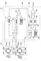
- FIG. 1 is a cross-sectional view of a physical quantity sensor according to the first embodiment of the present disclosure.
- 2 is a cross-sectional view of the acceleration sensor shown in FIG.
- FIG. 3 is a plan view of the sensor unit shown in FIG. 4 is a plan view of the angular velocity sensor shown in FIG.
- FIG. 5 is a sectional view taken along the line VV in FIG. 6 is a diagram showing a circuit configuration of the angular velocity sensor and the circuit board shown in FIG.
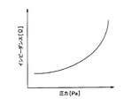
- FIG. 7 is a diagram showing the relationship between pressure and impedance
- FIG. 8 is a diagram illustrating the relationship between the pressure in the accommodation space when a leak occurs in the hermetic chamber and the ratio of the volume of the hermetic chamber to the volume of the accommodation space.
- the physical quantity sensor includes a case 10, and the case 10 includes a storage portion 11 and a lid portion 12.
- the accommodating portion 11 is formed by laminating a plurality of ceramic layers such as alumina, the first concave portion 13 is formed on one surface 11a, and the second concave portion 14 is formed on the bottom surface of the first concave portion 13, whereby the accommodating space 15 is configured. It has a box shape. And in the accommodating part 11, the internal connection terminals 16a and 16b are formed in the inner wall surface (the wall surface of the 1st recessed part 13, and the wall surface of the 2nd recessed part 14), and the external connection terminal which is not shown in figure is formed in the outer wall surface. The internal connection terminals 16a and 16b and the external connection terminals are appropriately electrically connected by an inner layer wiring (not shown) formed inside.
- the lid portion 12 is made of metal or the like, and hermetically seals the accommodation space 15 by being welded or joined to the one surface 11a of the accommodation portion 11.
- the accommodation space 15 is set to a vacuum pressure, for example, 1 Pa.
- the acceleration sensor 20, the angular velocity sensor 30, and the circuit board 40 are accommodated, respectively.
- the circuit board 40 is disposed on the bottom surface of the second recess 14 via an adhesive 51, and the acceleration sensor 20 is laminated on the circuit board 40 via an adhesive 52.
- the circuit board 40 is electrically connected to the internal connection terminals 16 b via the bonding wires 61, and the acceleration sensor 20 is electrically connected to the circuit board 40 via the bonding wires 62.
- the angular velocity sensor 30 is disposed on the bottom surface of the first recess 13 via the adhesive 53. More specifically, the angular velocity sensor 30 has an outer peripheral portion 313, and the outer peripheral portion 313 is joined to the adhesive 53. The angular velocity sensor 30 is electrically connected to the internal connection terminal 16 a via the bonding wire 63.
- the acceleration sensor 20 has a package structure sealed at atmospheric pressure, and is arranged in the accommodation space 15 in a packaged state. Further, the angular velocity sensor 30 is arranged in the accommodation space 15 as it is. For this reason, the acceleration sensor 20 detects acceleration under atmospheric pressure, and the angular velocity sensor 30 detects angular velocity under vacuum pressure.
- the acceleration sensor 20 has a package structure including a sensor unit 201 and a cap unit 202, as shown in FIG.
- the sensor unit 201 is configured using an SOI (Silicon on Insulator) substrate 214 in which a support substrate 211, an insulating film 212, and a semiconductor layer 213 are sequentially stacked.
- SOI Silicon on Insulator
- the support substrate 211 and the semiconductor layer 213 are formed of a silicon substrate or the like
- the insulating film 212 is formed of an oxide film or the like.
- the well-known micromachine processing is performed on the SOI substrate 214 to form the first sensing unit 215.
- the semiconductor layer 213 is formed with a movable portion 220 having a comb-shaped beam structure, a first fixed portion 230, and a second fixed portion 240 by forming the groove portion 216.
- a first sensing unit 215 that outputs a sensor signal corresponding to the acceleration is formed by the beam structure.
- an opening 217 that is removed in a rectangular shape by sacrificial layer etching or the like is formed in a portion of the insulating film 212 corresponding to the region where the beam structures 220 to 240 are formed.
- the movable portion 220 is disposed so as to cross the opening 217, and both ends in the longitudinal direction of the rectangular weight portion 221 are integrally connected to the anchor portions 223a and 223b via the beam portion 222.
- the anchor portions 223 a and 223 b are supported on the support substrate 211 via the insulating film 212 at the opening edge of the opening 217. Thereby, the weight part 221 and the beam part 222 are in a state of facing the opening part 217. 2 corresponds to a cross-sectional view taken along the line II-II in FIG.
- the beam portion 222 has a rectangular frame shape in which two parallel beams are connected at both ends thereof, and has a spring function of being displaced in a direction perpendicular to the longitudinal direction of the two beams. Specifically, when the beam portion 222 receives an acceleration including a component in a direction along the longitudinal direction of the weight portion 221, the beam portion 221 is displaced in the longitudinal direction, and the original state according to the disappearance of the acceleration. To restore. Therefore, the weight portion 221 connected to the support substrate 211 via the beam portion 222 is displaced in the displacement direction of the beam portion 222 when acceleration is applied.
- the movable part 220 includes a plurality of movable electrodes 224 that are integrally projected in opposite directions from both side surfaces of the weight part 221 in a direction orthogonal to the longitudinal direction of the weight part 221.
- four movable electrodes 224 are formed on the left side and the right side of the weight part 221 so as to face the opening 217.
- Each movable electrode 224 is formed integrally with the weight portion 221 and the beam portion 222, and can be displaced in the longitudinal direction of the weight portion 221 together with the weight portion 221 when the beam portion 222 is displaced.
- the first fixing portion 230 and the second fixing portion 240 are supported by the support substrate 211 via the insulating film 212 at the opposite side portions where the anchor portions 223a and 223b are not supported among the opening edge portions of the opening portion 217. ing. That is, the first fixed part 230 and the second fixed part 240 are arranged so as to sandwich the movable part 220. In FIG. 3, the first fixed portion 230 is disposed on the left side of the paper with respect to the movable portion 220, and the second fixed portion 240 is disposed on the right side of the paper with respect to the movable portion 220.
- the first fixing part 230 and the second fixing part 240 are electrically independent from each other.
- first fixed portion 230 and the second fixed portion 240 are a plurality of first fixed electrodes 231 and second fixed electrodes that are arranged to face each other in parallel with the side surface of the movable electrode 224 so as to have a predetermined detection interval.
- the four first fixed electrodes 231 and four second fixed electrodes 241 are formed in FIG. 3 and are arranged in a comb shape so as to mesh with the gaps of the comb teeth in the movable electrode 224. And it is in the state which faced the opening part 217 by being supported by each wiring part 232 and 242 in the shape of a cantilever.
- the above is the configuration of the sensor unit 201 in the present embodiment.
- the cap portion 202 has an insulating film 252 formed on one surface side of the substrate 251 made of silicon or the like facing the sensor portion 201 and insulated on the other surface opposite to the one surface.
- a film 253 was formed.
- the insulating film 252 is joined to the sensor part 201 (semiconductor layer 213).
- the insulating film 252 and the sensor unit 201 (semiconductor layer 213) are bonded by so-called direct bonding or the like in which the bonding surfaces of the insulating film 252 and the semiconductor layer 213 are activated and bonded.
- the cap portion 202 has a recess 254 formed at a portion facing the first sensing portion 215.
- the airtight chamber 255 is comprised in the space containing this hollow part 254, and the 1st sensing part 215 formed in the sensor part 201 is airtightly sealed to the airtight chamber 255. It has been stopped.
- the hermetic chamber 255 is at atmospheric pressure. That is, in the present embodiment, the acceleration sensor 20 has a package structure in which the first sensing unit 215 is hermetically sealed in the hermetic chamber 255 that is set to atmospheric pressure.
- the cap portion 202 is formed with a plurality of through holes 256 (only one is shown in FIG. 2) that penetrates the cap portion 202 and the sensor portion 201 in the stacking direction.
- the through hole 256 is formed to expose predetermined portions of the anchor portion 223b, the first wiring portion 232, and the second wiring portion 242.
- An insulating film 257 made of TEOS (tetraethyl orthosilicate) or the like is formed on the wall surface of the through hole 256, and a through electrode 258 made of Al or the like is appropriately formed on the insulating film 257 with the anchor portion 223b and
- the first wiring part 232 and the second wiring part 242 are formed so as to be electrically connected.
- a pad portion 259 that is electrically connected to the circuit board 40 is formed on the insulating film 253.
- a protective film 260 is formed on the insulating film 253, the through electrode 258, and the pad portion 259, and a contact hole 260 a that exposes the pad portion 259 is formed in the protective film 260.
- the acceleration sensor 20 when the acceleration is applied, the weight portion 221 is displaced according to the acceleration, whereby the capacitance between the movable electrode 224, the first fixed electrode 231, and the second fixed electrode 241 changes. To do. For this reason, a sensor signal corresponding to the acceleration (capacity) is output from the acceleration sensor 20.
- the angular velocity sensor 30 includes a sensor unit 301 configured using a substrate 310 such as quartz or PZT (lead zirconate titanate) as a piezoelectric material.
- the substrate 310 is subjected to well-known micromachining to form a groove portion 311, and the groove portion 311 defines a vibrating body 312 and an outer peripheral portion 313.
- the vibrating body 312 In the vibrating body 312, the first drive piece 314, the second drive piece 315, and the detection piece 316 are held by the base portion 317, and the base portion 317 is fixed to the outer peripheral portion 313 via the beam portion 318. More specifically, the vibrating body 312 is a so-called tripod tuning fork type in which the first drive piece 314, the second drive piece 315, and the detection piece 316 are arranged so as to protrude from the base 317 in the same direction. Is disposed between the first drive piece 314 and the second drive piece 315.
- the beam part 318 relieves the stress which generate
- the first drive piece 314, the second drive piece 315, and the detection piece 316 are front surfaces 314 a, 315 a, 316 a, rear surfaces 314 b, 315 b, 316 b that are parallel to the surface direction of the substrate 310. , Side bars 314 c, 314 d, 315 c, 315 d, 316 c, and 316 d, and a bar shape having a rectangular cross section.
- a driving electrode 319a is formed on the front surface 314a
- a driving electrode 319b is formed on the back surface 314b
- common electrodes 319c and 319d are formed on the side surfaces 314c and 314d.
- the drive electrode 320a is formed on the front surface 315a
- the drive electrode 320b is formed on the back surface 315b
- the common electrodes 320c and 320d are formed on the side surfaces 315c and 315d.
- a detection electrode 321a is formed on the front surface 316a
- a detection electrode 321b is formed on the back surface 316b
- common electrodes 321c and 321d are formed on the side surfaces 316c and 316d.
- the second sensing unit 322 includes the first drive piece 314 and the second drive piece 315, the detection piece 316, the drive electrodes 319a to 320b, the detection electrodes 321a and 321b, and the common electrodes 319c to 321d. Has been.
- the outer peripheral portion 313 is electrically connected to the drive electrodes 319a to 320b, the detection electrodes 321a and 321b, and the common electrodes 319c to 321d via a wiring layer (not shown) and the circuit board 40.
- a plurality of pad portions 323 that are electrically connected to each other are formed.
- the second sensing unit 322 is not hermetically sealed in the hermetic chamber.
- the first drive piece 314 and the second drive piece 315 are vibrated in the arrangement direction of the first drive piece 314, the second drive piece 315, and the detection piece 316 (the left and right direction in FIG. 4). The angular velocity is detected in the state.
- the first drive piece 314 and the second drive piece 315 are along the protruding direction with respect to the base 317 of the first drive piece 314 and the second drive piece 315.
- a pair of Coriolis forces that are directions and opposite directions are periodically generated. For this reason, the moment generated by the Coriolis force is transmitted to the detection piece 316 via the base 317, so that the detection piece 316 vibrates in the arrangement direction of the first drive piece 314, the second drive piece 315, and the detection piece 316. (Bending), a charge corresponding to the angular velocity is generated in the detection piece 316. Therefore, a sensor signal corresponding to the angular velocity (charge) is output from the angular velocity sensor 30.
- the circuit board 40 includes an angular velocity sensor control circuit 410 that drives the angular velocity sensor 30, a self-diagnosis circuit 420, an acceleration sensor control circuit (not shown) that controls the acceleration sensor 20, and each sensor. It has a processing circuit (not shown) for processing signals.
- the detection piece 316 is omitted.
- the angular velocity sensor control circuit 410 includes a drive circuit 411, a charge amplifier 412, a rectifier circuit 413, a first reference voltage generation circuit 414, a differential amplifier 415, and the like.
- the self-diagnosis circuit 420 includes a low-pass filter 421, a second reference voltage generation circuit 422, an adder 423, a subtractor 424, a window comparator 425, and the like.
- the drive circuit 411 includes an AGC (Auto Gain Control) circuit and is connected to the drive electrodes 319a and 319b of the first drive piece 314 and the drive electrode 320b of the second drive piece 315. Then, a fixed drive signal whose amplification factor is adjusted based on the voltage signal input from the charge amplifier 412 and the difference signal 430 input from the differential amplifier 415 is applied to the drive electrodes 319a, 319b, and 320b. That is, the adjusted drive signal is applied to the drive electrodes 319a, 319b, and 320b so that the vibration amplitudes of the first drive piece 314 and the second drive piece 315 are constant.
- AGC Automatic Gain Control
- a pulsed drive signal (carrier wave) having a predetermined amplitude and frequency is applied to the drive electrodes 319a and 319b of the first drive piece 314.
- a drive signal (carrier wave) that is 180 ° out of phase with the drive signal (carrier wave) applied to the drive electrodes 319a and 319b is applied to the drive electrode 320b of the second drive piece 315. Accordingly, the first drive piece 314 and the second drive piece 315 vibrate in the arrangement direction of the first drive piece 314, the second drive piece 315, and the detection piece 316.
- the charge amplifier 412 is connected to the drive electrode 320a of the second drive piece 315 and is connected to the drive circuit 411 and the rectifier circuit 413. Then, the electric charge generated in the drive electrode 320a due to the vibration of the second drive piece 315 is converted into a voltage signal, and the voltage signal is input to the drive circuit 411 and the rectifier circuit 413.
- the electric charge generated at the drive electrode 320 a of the second drive piece 315 changes according to the vibration state of the second drive piece 315. That is, it changes according to the pressure (detection environment) around the second drive piece 315 (vibrating body 312).
- the rectifier circuit 413 is connected to the differential amplifier 415, generates a DC voltage corresponding to the vibration amplitude of the second drive piece 315 from the voltage signal input from the charge amplifier 412, and inputs the DC voltage to the differential amplifier 415.
- the first reference voltage generation circuit 414 is connected to the differential amplifier 415 and inputs the first reference voltage to the differential amplifier 415.
- the differential amplifier 415 is connected to the drive circuit 411, the low-pass filter 421, and the window comparator 425. Then, a difference signal 430 between the DC voltage input from the rectifier circuit 413 and the first reference voltage input from the first reference voltage generation circuit 414 is input to the drive circuit 411, the low-pass filter 421, and the window comparator 425.
- the difference signal 430 output from the differential amplifier 415 is also a signal according to the detection environment.
- the differential amplifier 415 corresponds to a detection unit, and the difference signal 430 corresponds to a detection signal.
- the low pass filter 421 has a large time constant and is connected to the adder 423 and the subtractor 424.
- the difference signal 430 When the difference signal 430 is input, an output signal that gently follows the difference signal 430 is generated, and the output signal is input to the adder 423 and the subtractor 424.
- the low-pass filter 421 basically generates an output having a voltage equivalent to that of the difference signal 430.
- the difference signal 430 fluctuates rapidly, the low-pass filter 421 can follow the signal so as to completely match it. Instead, an output signal that follows in a slightly delayed state is generated.
- a filter having a cutoff frequency of about 0.1 Hz or 0.01 Hz is used as the low-pass filter 421 in order to absorb temperature fluctuation and aging.
- the second reference voltage generation circuit 422 is connected to the adder 423 and the subtractor 424, generates a second reference voltage, and inputs the second reference voltage to the adder 423 and the subtractor 424. This second reference voltage determines the range of the determination threshold value in the window comparator 425.
- the adder 423 is connected to the window comparator 425, and inputs the upper reference voltage 431 obtained by adding the second reference voltage to the output of the low-pass filter 421 to the window comparator 425.
- the subtractor 424 is connected to the window comparator 425, and inputs the lower limit reference voltage 432 obtained by subtracting the second reference voltage from the output of the low-pass filter 421 to the window comparator 425.
- the window comparator 425 includes the voltage of the difference signal 430 between the normal voltage range defined by the upper limit reference voltage 431 input from the adder 423 and the lower limit reference voltage 432 input from the subtractor 424. Determine whether. Then, the window comparator 425 outputs a diagnosis detection signal Vout according to whether or not the voltage of the difference signal 430 is within the normal voltage range. For example, when the voltage of the difference signal 430 is within the normal voltage range, the window comparator 425 outputs a high-level voltage signal indicating that the diagnosis signal Vout is normal. Further, when the voltage of the difference signal 430 is not within the normal voltage range, a low level detection signal indicating that the diagnosis signal Vout is abnormal is output.
- the window comparator 425 corresponds to a self-diagnosis unit.
- the common electrodes 319c to 320d are connected to the ground potential.
- the voltage signal converted by the charge amplifier 412 changes, and the difference signal 430 output from the differential amplifier 415 changes. That is, the differential signal 430 corresponding to the detection environment of the vibrating body 312 is output from the differential amplifier 415.
- the difference signal 430 is input from the differential amplifier 415 to the window comparator 425, and it is determined whether or not the difference signal 430 is within the normal voltage range.
- the window comparator 425 outputs an abnormal voltage as the diagnosis detection signal Vout, and it is detected that the pressure in the accommodation space 15 has fluctuated. . That is, the detection environment of the angular velocity sensor 30 is self-diagnosed.
- the detection environment of the angular velocity sensor 30 is abnormal, a leak has occurred in the airtight chamber 255 of the acceleration sensor 20, so that the self-diagnosis can be made that the detection environment of the acceleration sensor 20 is also abnormal.
- the ratio of the volume of the hermetic chamber 255 to the volume of the accommodation space 15 is set to 1.0 ⁇ 10 ⁇ 7 or more. As shown in FIG. 8, when the ratio of the volume of the airtight chamber 255 to the volume of the storage space 15 is less than 1.0 ⁇ 10 ⁇ 7 , even if a leak occurs in the airtight chamber 255, This is because the pressure does not easily fluctuate.
- the vibration state of the first drive piece 314 and the second drive piece 315 is detected, and the difference signal 430 corresponding to the vibration state is output from the differential amplifier 415. That is, when a leak occurs in the hermetic chamber 255 and the pressure in the accommodation space 15 fluctuates, the vibration state of the first drive piece 314 and the second drive piece 315 changes, and therefore a difference corresponding to the pressure in the accommodation space 15. A signal 430 is output from the differential amplifier 415.
- the window comparator 425 determines whether the difference signal 430 is within the normal voltage range. For this reason, the self-diagnosis of the detection environment of the angular velocity sensor 30 (pressure in the accommodation space 15) can be performed. Further, when the detection environment of the angular velocity sensor 30 is abnormal, a leak has occurred in the airtight chamber 255 of the acceleration sensor 20, so that it can be self-diagnosed that the detection environment of the acceleration sensor 20 is also abnormal. Therefore, when various processes are performed using the signals output from the acceleration sensor 20 and the angular velocity sensor 30, it is possible to suppress erroneous processes.
- the acceleration sensor 20 is packaged, but the angular velocity sensor 30 may be packaged.
- the accommodation space 15 is set to atmospheric pressure, and the airtight chamber that seals the second sensing unit 322 of the angular velocity sensor 30 is set to a vacuum pressure.
- both the acceleration sensor 20 and the angular velocity sensor 30 may be packaged.
- the storage space 15 may be set to atmospheric pressure or a vacuum pressure.
- the angular velocity sensor 30 may not be a tripod tuning fork type.
- the angular velocity sensor 30 may be a so-called T-type tuning fork type in which the first drive piece 314, the second drive piece 315, and the detection piece 316 protrude from both sides with the base portion 317 interposed therebetween.
- the angular velocity sensor 30 may be a so-called H-type tuning fork, a normal tuning fork type, or the like.
- the angular velocity sensor 30 may be a capacitive type. That is, the configuration of the angular velocity sensor 30 is not particularly limited as long as the angular velocity is detected while vibrating the vibrating body 312.
- the acceleration sensor 20 may be a piezoelectric type.
Landscapes
- Engineering & Computer Science (AREA)
- Physics & Mathematics (AREA)
- General Physics & Mathematics (AREA)
- Radar, Positioning & Navigation (AREA)
- Remote Sensing (AREA)
- Manufacturing & Machinery (AREA)
- Signal Processing (AREA)
- Gyroscopes (AREA)
- Pressure Sensors (AREA)
Priority Applications (2)
| Application Number | Priority Date | Filing Date | Title |
|---|---|---|---|
| DE112015002785.8T DE112015002785T5 (de) | 2014-06-12 | 2015-06-11 | Sensor für eine physikalische Grösse |
| US15/307,859 US10393523B2 (en) | 2014-06-12 | 2015-06-11 | Physical quantity sensor |
Applications Claiming Priority (2)
| Application Number | Priority Date | Filing Date | Title |
|---|---|---|---|
| JP2014-121690 | 2014-06-12 | ||
| JP2014121690A JP6409351B2 (ja) | 2014-06-12 | 2014-06-12 | 物理量センサ |
Publications (1)
| Publication Number | Publication Date |
|---|---|
| WO2015190104A1 true WO2015190104A1 (ja) | 2015-12-17 |
Family
ID=54833215
Family Applications (1)
| Application Number | Title | Priority Date | Filing Date |
|---|---|---|---|
| PCT/JP2015/002919 Ceased WO2015190104A1 (ja) | 2014-06-12 | 2015-06-11 | 物理量センサ |
Country Status (4)
| Country | Link |
|---|---|
| US (1) | US10393523B2 (enExample) |
| JP (1) | JP6409351B2 (enExample) |
| DE (1) | DE112015002785T5 (enExample) |
| WO (1) | WO2015190104A1 (enExample) |
Families Citing this family (4)
| Publication number | Priority date | Publication date | Assignee | Title |
|---|---|---|---|---|
| JP6492739B2 (ja) | 2015-02-20 | 2019-04-03 | セイコーエプソン株式会社 | 回路装置、物理量検出装置、電子機器及び移動体 |
| JP6586735B2 (ja) * | 2015-02-20 | 2019-10-09 | セイコーエプソン株式会社 | 回路装置、物理量検出装置、電子機器及び移動体 |
| KR102437764B1 (ko) | 2017-12-20 | 2022-08-30 | 삼성전자주식회사 | 센서 패키지, 센서 패키지의 제조 방법, 및 리드 구조체의 제조 방법 |
| JP6996344B2 (ja) * | 2018-02-28 | 2022-01-17 | セイコーエプソン株式会社 | センサーデバイス、力検出装置およびロボット |
Citations (4)
| Publication number | Priority date | Publication date | Assignee | Title |
|---|---|---|---|---|
| JPH10206273A (ja) * | 1997-01-21 | 1998-08-07 | Toyota Motor Corp | 角速度センサの気密性確認方法及び装置 |
| JP2011017693A (ja) * | 2009-06-09 | 2011-01-27 | Denso Corp | 半導体力学量センサの製造方法及び半導体力学量センサ |
| JP2011179821A (ja) * | 2010-02-26 | 2011-09-15 | Hitachi Automotive Systems Ltd | 複合センサの製造方法 |
| JP2013120179A (ja) * | 2011-12-09 | 2013-06-17 | Panasonic Corp | 角速度センサ |
Family Cites Families (17)
| Publication number | Priority date | Publication date | Assignee | Title |
|---|---|---|---|---|
| JP3123352B2 (ja) | 1994-06-29 | 2001-01-09 | 株式会社デンソー | 漏れ測定方法及びその装置 |
| JPH1151802A (ja) * | 1997-07-31 | 1999-02-26 | River Eletec Kk | 圧電素子用パッケージの気密検査方法 |
| JP3435665B2 (ja) | 2000-06-23 | 2003-08-11 | 株式会社村田製作所 | 複合センサ素子およびその製造方法 |
| JP3512004B2 (ja) | 2000-12-20 | 2004-03-29 | トヨタ自動車株式会社 | 力学量検出装置 |
| DE102004027501A1 (de) | 2004-06-04 | 2005-12-22 | Robert Bosch Gmbh | Mikromechanisches Bauelement mit mehreren Kavernen und Herstellungsverfahren |
| JP2006010659A (ja) | 2004-06-21 | 2006-01-12 | Microstone Corp | 振動ジャイロスコープ |
| JP4543869B2 (ja) | 2004-10-15 | 2010-09-15 | 株式会社デンソー | 振動型角速度センサにおけるセンサ回路 |
| JP5222457B2 (ja) * | 2005-09-26 | 2013-06-26 | 株式会社日立製作所 | センサおよびセンサモジュール |
| DE102006016260B4 (de) | 2006-04-06 | 2024-07-18 | Fraunhofer-Gesellschaft zur Förderung der angewandten Forschung e.V. | Vielfach-Bauelement mit mehreren aktive Strukturen enthaltenden Bauteilen (MEMS) zum späteren Vereinzeln, flächiges Substrat oder flächig ausgebildete Kappenstruktur, in der Mikrosystemtechnik einsetzbares Bauteil mit aktiven Strukturen, Einzelsubstrat oder Kappenstruktur mit aktiven Strukturen und Verfahren zum Herstellen eines Vielfach-Bauelements |
| CN101796374A (zh) * | 2007-09-03 | 2010-08-04 | 松下电器产业株式会社 | 惯性力传感器 |
| JP5319122B2 (ja) | 2008-01-21 | 2013-10-16 | 日立オートモティブシステムズ株式会社 | 慣性センサ |
| US7800190B2 (en) * | 2008-06-16 | 2010-09-21 | Honeywell International Inc. | Getter on die in an upper sense plate designed system |
| JP5321150B2 (ja) | 2009-03-05 | 2013-10-23 | セイコーエプソン株式会社 | 複合センサー |
| JP2010204061A (ja) * | 2009-03-06 | 2010-09-16 | Panasonic Corp | 電子部品及びその製造方法 |
| US20120142136A1 (en) | 2010-12-01 | 2012-06-07 | Honeywell International Inc. | Wafer level packaging process for mems devices |
| US20140260612A1 (en) * | 2011-11-28 | 2014-09-18 | Hitachi Automotive Systems, Ltd. | Composite Sensor and Method for Manufacturing The Same |
| JP6435631B2 (ja) | 2014-04-23 | 2018-12-12 | 株式会社デンソー | 角速度センサ |
-
2014
- 2014-06-12 JP JP2014121690A patent/JP6409351B2/ja active Active
-
2015
- 2015-06-11 US US15/307,859 patent/US10393523B2/en active Active
- 2015-06-11 DE DE112015002785.8T patent/DE112015002785T5/de active Pending
- 2015-06-11 WO PCT/JP2015/002919 patent/WO2015190104A1/ja not_active Ceased
Patent Citations (4)
| Publication number | Priority date | Publication date | Assignee | Title |
|---|---|---|---|---|
| JPH10206273A (ja) * | 1997-01-21 | 1998-08-07 | Toyota Motor Corp | 角速度センサの気密性確認方法及び装置 |
| JP2011017693A (ja) * | 2009-06-09 | 2011-01-27 | Denso Corp | 半導体力学量センサの製造方法及び半導体力学量センサ |
| JP2011179821A (ja) * | 2010-02-26 | 2011-09-15 | Hitachi Automotive Systems Ltd | 複合センサの製造方法 |
| JP2013120179A (ja) * | 2011-12-09 | 2013-06-17 | Panasonic Corp | 角速度センサ |
Also Published As
| Publication number | Publication date |
|---|---|
| US10393523B2 (en) | 2019-08-27 |
| US20170059320A1 (en) | 2017-03-02 |
| JP6409351B2 (ja) | 2018-10-24 |
| DE112015002785T5 (de) | 2017-03-02 |
| JP2016001158A (ja) | 2016-01-07 |
Similar Documents
| Publication | Publication Date | Title |
|---|---|---|
| US9835641B2 (en) | Angular velocity detection device and angular velocity sensor including the same | |
| CN103376100B (zh) | 振动片和陀螺传感器、以及电子设备和移动体 | |
| US10119821B2 (en) | Angular velocity sensor | |
| US20190301866A1 (en) | Physical quantity sensor | |
| JP4599848B2 (ja) | 角速度センサ | |
| JP6409351B2 (ja) | 物理量センサ | |
| JP6372361B2 (ja) | 複合センサ | |
| CN103105261A (zh) | 物理量检测器 | |
| JP6372450B2 (ja) | 複合センサ | |
| JP6435631B2 (ja) | 角速度センサ | |
| JP4974359B2 (ja) | 力学量センサ | |
| JP2008275325A (ja) | センサ装置 | |
| CN105388323B (zh) | 振动式传感器装置 | |
| JP4869001B2 (ja) | 振動ジャイロ | |
| JP4600590B2 (ja) | 角速度センサ | |
| JPH0989569A (ja) | 振動ジャイロ | |
| JP4333474B2 (ja) | 圧電振動子 | |
| JP5321812B2 (ja) | 物理量センサーおよび物理量測定装置 | |
| JP2006226799A (ja) | 力学量センサ | |
| WO2014030492A1 (ja) | 慣性力センサ | |
| JP5776184B2 (ja) | センサ装置 | |
| JP2017122678A (ja) | 物理量センサ | |
| JP2011013063A (ja) | 圧力センサー及び圧力センサーの圧力検出方法 |
Legal Events
| Date | Code | Title | Description |
|---|---|---|---|
| 121 | Ep: the epo has been informed by wipo that ep was designated in this application |
Ref document number: 15806460 Country of ref document: EP Kind code of ref document: A1 |
|
| WWE | Wipo information: entry into national phase |
Ref document number: 15307859 Country of ref document: US |
|
| WWE | Wipo information: entry into national phase |
Ref document number: 112015002785 Country of ref document: DE |
|
| 122 | Ep: pct application non-entry in european phase |
Ref document number: 15806460 Country of ref document: EP Kind code of ref document: A1 |