WO2015190104A1 - 物理量センサ - Google Patents
物理量センサ Download PDFInfo
- Publication number
- WO2015190104A1 WO2015190104A1 PCT/JP2015/002919 JP2015002919W WO2015190104A1 WO 2015190104 A1 WO2015190104 A1 WO 2015190104A1 JP 2015002919 W JP2015002919 W JP 2015002919W WO 2015190104 A1 WO2015190104 A1 WO 2015190104A1
- Authority
- WO
- WIPO (PCT)
- Prior art keywords
- sensor
- angular velocity
- acceleration
- detection
- velocity sensor
- Prior art date
Links
Images


Classifications
-
- G—PHYSICS
- G01—MEASURING; TESTING
- G01C—MEASURING DISTANCES, LEVELS OR BEARINGS; SURVEYING; NAVIGATION; GYROSCOPIC INSTRUMENTS; PHOTOGRAMMETRY OR VIDEOGRAMMETRY
- G01C19/00—Gyroscopes; Turn-sensitive devices using vibrating masses; Turn-sensitive devices without moving masses; Measuring angular rate using gyroscopic effects
- G01C19/56—Turn-sensitive devices using vibrating masses, e.g. vibratory angular rate sensors based on Coriolis forces
- G01C19/5607—Turn-sensitive devices using vibrating masses, e.g. vibratory angular rate sensors based on Coriolis forces using vibrating tuning forks
- G01C19/5614—Signal processing
-
- G—PHYSICS
- G01—MEASURING; TESTING
- G01C—MEASURING DISTANCES, LEVELS OR BEARINGS; SURVEYING; NAVIGATION; GYROSCOPIC INSTRUMENTS; PHOTOGRAMMETRY OR VIDEOGRAMMETRY
- G01C19/00—Gyroscopes; Turn-sensitive devices using vibrating masses; Turn-sensitive devices without moving masses; Measuring angular rate using gyroscopic effects
- G01C19/56—Turn-sensitive devices using vibrating masses, e.g. vibratory angular rate sensors based on Coriolis forces
- G01C19/5607—Turn-sensitive devices using vibrating masses, e.g. vibratory angular rate sensors based on Coriolis forces using vibrating tuning forks
- G01C19/5628—Manufacturing; Trimming; Mounting; Housings
-
- G—PHYSICS
- G01—MEASURING; TESTING
- G01C—MEASURING DISTANCES, LEVELS OR BEARINGS; SURVEYING; NAVIGATION; GYROSCOPIC INSTRUMENTS; PHOTOGRAMMETRY OR VIDEOGRAMMETRY
- G01C25/00—Manufacturing, calibrating, cleaning, or repairing instruments or devices referred to in the other groups of this subclass
-
- G—PHYSICS
- G01—MEASURING; TESTING
- G01P—MEASURING LINEAR OR ANGULAR SPEED, ACCELERATION, DECELERATION, OR SHOCK; INDICATING PRESENCE, ABSENCE, OR DIRECTION, OF MOVEMENT
- G01P15/00—Measuring acceleration; Measuring deceleration; Measuring shock, i.e. sudden change of acceleration
- G01P15/02—Measuring acceleration; Measuring deceleration; Measuring shock, i.e. sudden change of acceleration by making use of inertia forces using solid seismic masses
- G01P15/08—Measuring acceleration; Measuring deceleration; Measuring shock, i.e. sudden change of acceleration by making use of inertia forces using solid seismic masses with conversion into electric or magnetic values
- G01P15/125—Measuring acceleration; Measuring deceleration; Measuring shock, i.e. sudden change of acceleration by making use of inertia forces using solid seismic masses with conversion into electric or magnetic values by capacitive pick-up
-
- G—PHYSICS
- G01—MEASURING; TESTING
- G01P—MEASURING LINEAR OR ANGULAR SPEED, ACCELERATION, DECELERATION, OR SHOCK; INDICATING PRESENCE, ABSENCE, OR DIRECTION, OF MOVEMENT
- G01P21/00—Testing or calibrating of apparatus or devices covered by the preceding groups
-
- G—PHYSICS
- G01—MEASURING; TESTING
- G01P—MEASURING LINEAR OR ANGULAR SPEED, ACCELERATION, DECELERATION, OR SHOCK; INDICATING PRESENCE, ABSENCE, OR DIRECTION, OF MOVEMENT
- G01P15/00—Measuring acceleration; Measuring deceleration; Measuring shock, i.e. sudden change of acceleration
- G01P15/02—Measuring acceleration; Measuring deceleration; Measuring shock, i.e. sudden change of acceleration by making use of inertia forces using solid seismic masses
- G01P15/08—Measuring acceleration; Measuring deceleration; Measuring shock, i.e. sudden change of acceleration by making use of inertia forces using solid seismic masses with conversion into electric or magnetic values
- G01P2015/0805—Measuring acceleration; Measuring deceleration; Measuring shock, i.e. sudden change of acceleration by making use of inertia forces using solid seismic masses with conversion into electric or magnetic values being provided with a particular type of spring-mass-system for defining the displacement of a seismic mass due to an external acceleration
- G01P2015/0808—Measuring acceleration; Measuring deceleration; Measuring shock, i.e. sudden change of acceleration by making use of inertia forces using solid seismic masses with conversion into electric or magnetic values being provided with a particular type of spring-mass-system for defining the displacement of a seismic mass due to an external acceleration for defining in-plane movement of the mass, i.e. movement of the mass in the plane of the substrate
- G01P2015/0811—Measuring acceleration; Measuring deceleration; Measuring shock, i.e. sudden change of acceleration by making use of inertia forces using solid seismic masses with conversion into electric or magnetic values being provided with a particular type of spring-mass-system for defining the displacement of a seismic mass due to an external acceleration for defining in-plane movement of the mass, i.e. movement of the mass in the plane of the substrate for one single degree of freedom of movement of the mass
- G01P2015/0814—Measuring acceleration; Measuring deceleration; Measuring shock, i.e. sudden change of acceleration by making use of inertia forces using solid seismic masses with conversion into electric or magnetic values being provided with a particular type of spring-mass-system for defining the displacement of a seismic mass due to an external acceleration for defining in-plane movement of the mass, i.e. movement of the mass in the plane of the substrate for one single degree of freedom of movement of the mass for translational movement of the mass, e.g. shuttle type
-
- H—ELECTRICITY
- H01—ELECTRIC ELEMENTS
- H01L—SEMICONDUCTOR DEVICES NOT COVERED BY CLASS H10
- H01L2224/00—Indexing scheme for arrangements for connecting or disconnecting semiconductor or solid-state bodies and methods related thereto as covered by H01L24/00
- H01L2224/01—Means for bonding being attached to, or being formed on, the surface to be connected, e.g. chip-to-package, die-attach, "first-level" interconnects; Manufacturing methods related thereto
- H01L2224/26—Layer connectors, e.g. plate connectors, solder or adhesive layers; Manufacturing methods related thereto
- H01L2224/31—Structure, shape, material or disposition of the layer connectors after the connecting process
- H01L2224/32—Structure, shape, material or disposition of the layer connectors after the connecting process of an individual layer connector
- H01L2224/321—Disposition
- H01L2224/32135—Disposition the layer connector connecting between different semiconductor or solid-state bodies, i.e. chip-to-chip
- H01L2224/32145—Disposition the layer connector connecting between different semiconductor or solid-state bodies, i.e. chip-to-chip the bodies being stacked
-
- H—ELECTRICITY
- H01—ELECTRIC ELEMENTS
- H01L—SEMICONDUCTOR DEVICES NOT COVERED BY CLASS H10
- H01L2224/00—Indexing scheme for arrangements for connecting or disconnecting semiconductor or solid-state bodies and methods related thereto as covered by H01L24/00
- H01L2224/01—Means for bonding being attached to, or being formed on, the surface to be connected, e.g. chip-to-package, die-attach, "first-level" interconnects; Manufacturing methods related thereto
- H01L2224/42—Wire connectors; Manufacturing methods related thereto
- H01L2224/47—Structure, shape, material or disposition of the wire connectors after the connecting process
- H01L2224/48—Structure, shape, material or disposition of the wire connectors after the connecting process of an individual wire connector
- H01L2224/4805—Shape
- H01L2224/4809—Loop shape
- H01L2224/48091—Arched
-
- H—ELECTRICITY
- H01—ELECTRIC ELEMENTS
- H01L—SEMICONDUCTOR DEVICES NOT COVERED BY CLASS H10
- H01L2224/00—Indexing scheme for arrangements for connecting or disconnecting semiconductor or solid-state bodies and methods related thereto as covered by H01L24/00
- H01L2224/01—Means for bonding being attached to, or being formed on, the surface to be connected, e.g. chip-to-package, die-attach, "first-level" interconnects; Manufacturing methods related thereto
- H01L2224/42—Wire connectors; Manufacturing methods related thereto
- H01L2224/47—Structure, shape, material or disposition of the wire connectors after the connecting process
- H01L2224/48—Structure, shape, material or disposition of the wire connectors after the connecting process of an individual wire connector
- H01L2224/481—Disposition
- H01L2224/48135—Connecting between different semiconductor or solid-state bodies, i.e. chip-to-chip
- H01L2224/48145—Connecting between different semiconductor or solid-state bodies, i.e. chip-to-chip the bodies being stacked
-
- H—ELECTRICITY
- H01—ELECTRIC ELEMENTS
- H01L—SEMICONDUCTOR DEVICES NOT COVERED BY CLASS H10
- H01L2224/00—Indexing scheme for arrangements for connecting or disconnecting semiconductor or solid-state bodies and methods related thereto as covered by H01L24/00
- H01L2224/73—Means for bonding being of different types provided for in two or more of groups H01L2224/10, H01L2224/18, H01L2224/26, H01L2224/34, H01L2224/42, H01L2224/50, H01L2224/63, H01L2224/71
- H01L2224/732—Location after the connecting process
- H01L2224/73251—Location after the connecting process on different surfaces
- H01L2224/73265—Layer and wire connectors
-
- H—ELECTRICITY
- H01—ELECTRIC ELEMENTS
- H01L—SEMICONDUCTOR DEVICES NOT COVERED BY CLASS H10
- H01L2924/00—Indexing scheme for arrangements or methods for connecting or disconnecting semiconductor or solid-state bodies as covered by H01L24/00
- H01L2924/15—Details of package parts other than the semiconductor or other solid state devices to be connected
- H01L2924/161—Cap
- H01L2924/1615—Shape
- H01L2924/16195—Flat cap [not enclosing an internal cavity]
Definitions
- the present disclosure describes a physical quantity in which an acceleration sensor formed with a sensing unit that outputs a sensor signal according to acceleration and an angular velocity sensor formed with a sensing unit that outputs a sensor signal according to angular velocity are accommodated in an accommodation space of a common case. It relates to sensors.
- the acceleration sensor since it is desired that the acceleration sensor is in a stationary state when no acceleration is applied, it is preferable to detect acceleration under atmospheric pressure where air damping (gas flow resistance) is large.
- the angular velocity sensor has a vibrating body and detects the angular velocity in a state where the vibrating body is vibrating. For this reason, it is preferable that the angular velocity sensor detects the angular velocity under a vacuum pressure with small air damping so that the vibrating body can easily vibrate.
- the pressure of the accommodation space is set to the vacuum pressure
- the angular velocity sensor is arranged in the accommodation space as it is.
- the acceleration sensor is arranged in the accommodation space in a package structure in which the sensing unit is hermetically sealed in an airtight chamber at atmospheric pressure.
- the acceleration sensor outputs a sensor signal corresponding to the applied acceleration even when the pressure in the hermetic chamber fluctuates.
- the angular velocity sensor outputs a sensor signal corresponding to the applied angular velocity even when the pressure in the accommodation space varies. That is, when the detection environment changes, acceleration and angular velocity are detected with the detection accuracy changed.
- the physical quantity sensor cannot grasp the detection environment. For this reason, when various processes, such as driving control of a vehicle, are performed using the sensor signal output from an acceleration sensor and the sensor signal output from an angular velocity sensor, an erroneous process may be performed.
- This indication aims at providing the physical quantity sensor which can self-diagnose the detection environment of an acceleration sensor and an angular velocity sensor in view of the above-mentioned point.
- the physical quantity sensor includes an acceleration sensor having a first sensing unit that outputs a sensor signal corresponding to acceleration, and a second sensing unit having a vibrating body that vibrates in a predetermined direction.
- the sensor includes an angular velocity sensor that outputs a sensor signal corresponding to the angular velocity from the sensing unit, and a case that has an accommodating space that is set to a predetermined pressure, and that accommodates the acceleration sensor and the angular velocity sensor in the accommodating space.
- At least one of the acceleration sensor and the angular velocity sensor has a cap portion disposed on the sensor portion where the sensing portion is formed, and the sensing portion is hermetically sealed in an airtight chamber configured between the sensor portion and the cap portion.
- Package structure having a first sensing unit that outputs a sensor signal corresponding to acceleration, and a second sensing unit having a vibrating body that vibrates in a predetermined direction.
- the sensor includes an angular velocity sensor that outputs a sensor signal corresponding to the angular velocity from
- the physical quantity sensor has a detection unit that outputs a detection signal corresponding to the vibration of the vibrating body in the angular velocity sensor, and a self-diagnosis unit that self-diagnose the detection environment of the angular velocity sensor based on the detection signal output from the detection unit. is doing.
- the self-diagnosis unit can self-diagnose the detection environment of the angular velocity sensor.
- the pressure in the housing space is a vacuum pressure
- the pressure in the housing space angular velocity Since the detection environment of the sensor fluctuates, the vibration state of the vibrating body changes. For this reason, it can be determined that the detection environment of the angular velocity sensor is abnormal based on the detection signal.
- the detection environment of the angular velocity sensor becomes abnormal when a leak occurs in the airtight chamber of the acceleration sensor that is a package structure. Therefore, when the angular velocity sensor is abnormal, the detection environment of the acceleration sensor is also abnormal. Can be determined. Therefore, when various processes are performed using signals output from the acceleration sensor and the angular velocity sensor, erroneous processes can be suppressed.
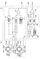
- FIG. 1 is a cross-sectional view of a physical quantity sensor according to the first embodiment of the present disclosure.
- 2 is a cross-sectional view of the acceleration sensor shown in FIG.
- FIG. 3 is a plan view of the sensor unit shown in FIG. 4 is a plan view of the angular velocity sensor shown in FIG.
- FIG. 5 is a sectional view taken along the line VV in FIG. 6 is a diagram showing a circuit configuration of the angular velocity sensor and the circuit board shown in FIG.
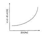
- FIG. 7 is a diagram showing the relationship between pressure and impedance
- FIG. 8 is a diagram illustrating the relationship between the pressure in the accommodation space when a leak occurs in the hermetic chamber and the ratio of the volume of the hermetic chamber to the volume of the accommodation space.
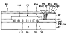
- the physical quantity sensor includes a case 10, and the case 10 includes a storage portion 11 and a lid portion 12.
- the accommodating portion 11 is formed by laminating a plurality of ceramic layers such as alumina, the first concave portion 13 is formed on one surface 11a, and the second concave portion 14 is formed on the bottom surface of the first concave portion 13, whereby the accommodating space 15 is configured. It has a box shape. And in the accommodating part 11, the internal connection terminals 16a and 16b are formed in the inner wall surface (the wall surface of the 1st recessed part 13, and the wall surface of the 2nd recessed part 14), and the external connection terminal which is not shown in figure is formed in the outer wall surface. The internal connection terminals 16a and 16b and the external connection terminals are appropriately electrically connected by an inner layer wiring (not shown) formed inside.
- the lid portion 12 is made of metal or the like, and hermetically seals the accommodation space 15 by being welded or joined to the one surface 11a of the accommodation portion 11.
- the accommodation space 15 is set to a vacuum pressure, for example, 1 Pa.
- the acceleration sensor 20, the angular velocity sensor 30, and the circuit board 40 are accommodated, respectively.
- the circuit board 40 is disposed on the bottom surface of the second recess 14 via an adhesive 51, and the acceleration sensor 20 is laminated on the circuit board 40 via an adhesive 52.
- the circuit board 40 is electrically connected to the internal connection terminals 16 b via the bonding wires 61, and the acceleration sensor 20 is electrically connected to the circuit board 40 via the bonding wires 62.
- the angular velocity sensor 30 is disposed on the bottom surface of the first recess 13 via the adhesive 53. More specifically, the angular velocity sensor 30 has an outer peripheral portion 313, and the outer peripheral portion 313 is joined to the adhesive 53. The angular velocity sensor 30 is electrically connected to the internal connection terminal 16 a via the bonding wire 63.
- the acceleration sensor 20 has a package structure sealed at atmospheric pressure, and is arranged in the accommodation space 15 in a packaged state. Further, the angular velocity sensor 30 is arranged in the accommodation space 15 as it is. For this reason, the acceleration sensor 20 detects acceleration under atmospheric pressure, and the angular velocity sensor 30 detects angular velocity under vacuum pressure.
- the acceleration sensor 20 has a package structure including a sensor unit 201 and a cap unit 202, as shown in FIG.
- the sensor unit 201 is configured using an SOI (Silicon on Insulator) substrate 214 in which a support substrate 211, an insulating film 212, and a semiconductor layer 213 are sequentially stacked.
- SOI Silicon on Insulator
- the support substrate 211 and the semiconductor layer 213 are formed of a silicon substrate or the like
- the insulating film 212 is formed of an oxide film or the like.
- the well-known micromachine processing is performed on the SOI substrate 214 to form the first sensing unit 215.
- the semiconductor layer 213 is formed with a movable portion 220 having a comb-shaped beam structure, a first fixed portion 230, and a second fixed portion 240 by forming the groove portion 216.
- a first sensing unit 215 that outputs a sensor signal corresponding to the acceleration is formed by the beam structure.
- an opening 217 that is removed in a rectangular shape by sacrificial layer etching or the like is formed in a portion of the insulating film 212 corresponding to the region where the beam structures 220 to 240 are formed.
- the movable portion 220 is disposed so as to cross the opening 217, and both ends in the longitudinal direction of the rectangular weight portion 221 are integrally connected to the anchor portions 223a and 223b via the beam portion 222.
- the anchor portions 223 a and 223 b are supported on the support substrate 211 via the insulating film 212 at the opening edge of the opening 217. Thereby, the weight part 221 and the beam part 222 are in a state of facing the opening part 217. 2 corresponds to a cross-sectional view taken along the line II-II in FIG.
- the beam portion 222 has a rectangular frame shape in which two parallel beams are connected at both ends thereof, and has a spring function of being displaced in a direction perpendicular to the longitudinal direction of the two beams. Specifically, when the beam portion 222 receives an acceleration including a component in a direction along the longitudinal direction of the weight portion 221, the beam portion 221 is displaced in the longitudinal direction, and the original state according to the disappearance of the acceleration. To restore. Therefore, the weight portion 221 connected to the support substrate 211 via the beam portion 222 is displaced in the displacement direction of the beam portion 222 when acceleration is applied.
- the movable part 220 includes a plurality of movable electrodes 224 that are integrally projected in opposite directions from both side surfaces of the weight part 221 in a direction orthogonal to the longitudinal direction of the weight part 221.
- four movable electrodes 224 are formed on the left side and the right side of the weight part 221 so as to face the opening 217.
- Each movable electrode 224 is formed integrally with the weight portion 221 and the beam portion 222, and can be displaced in the longitudinal direction of the weight portion 221 together with the weight portion 221 when the beam portion 222 is displaced.
- the first fixing portion 230 and the second fixing portion 240 are supported by the support substrate 211 via the insulating film 212 at the opposite side portions where the anchor portions 223a and 223b are not supported among the opening edge portions of the opening portion 217. ing. That is, the first fixed part 230 and the second fixed part 240 are arranged so as to sandwich the movable part 220. In FIG. 3, the first fixed portion 230 is disposed on the left side of the paper with respect to the movable portion 220, and the second fixed portion 240 is disposed on the right side of the paper with respect to the movable portion 220.
- the first fixing part 230 and the second fixing part 240 are electrically independent from each other.
- first fixed portion 230 and the second fixed portion 240 are a plurality of first fixed electrodes 231 and second fixed electrodes that are arranged to face each other in parallel with the side surface of the movable electrode 224 so as to have a predetermined detection interval.
- the four first fixed electrodes 231 and four second fixed electrodes 241 are formed in FIG. 3 and are arranged in a comb shape so as to mesh with the gaps of the comb teeth in the movable electrode 224. And it is in the state which faced the opening part 217 by being supported by each wiring part 232 and 242 in the shape of a cantilever.
- the above is the configuration of the sensor unit 201 in the present embodiment.
- the cap portion 202 has an insulating film 252 formed on one surface side of the substrate 251 made of silicon or the like facing the sensor portion 201 and insulated on the other surface opposite to the one surface.
- a film 253 was formed.
- the insulating film 252 is joined to the sensor part 201 (semiconductor layer 213).
- the insulating film 252 and the sensor unit 201 (semiconductor layer 213) are bonded by so-called direct bonding or the like in which the bonding surfaces of the insulating film 252 and the semiconductor layer 213 are activated and bonded.
- the cap portion 202 has a recess 254 formed at a portion facing the first sensing portion 215.
- the airtight chamber 255 is comprised in the space containing this hollow part 254, and the 1st sensing part 215 formed in the sensor part 201 is airtightly sealed to the airtight chamber 255. It has been stopped.
- the hermetic chamber 255 is at atmospheric pressure. That is, in the present embodiment, the acceleration sensor 20 has a package structure in which the first sensing unit 215 is hermetically sealed in the hermetic chamber 255 that is set to atmospheric pressure.
- the cap portion 202 is formed with a plurality of through holes 256 (only one is shown in FIG. 2) that penetrates the cap portion 202 and the sensor portion 201 in the stacking direction.
- the through hole 256 is formed to expose predetermined portions of the anchor portion 223b, the first wiring portion 232, and the second wiring portion 242.
- An insulating film 257 made of TEOS (tetraethyl orthosilicate) or the like is formed on the wall surface of the through hole 256, and a through electrode 258 made of Al or the like is appropriately formed on the insulating film 257 with the anchor portion 223b and
- the first wiring part 232 and the second wiring part 242 are formed so as to be electrically connected.
- a pad portion 259 that is electrically connected to the circuit board 40 is formed on the insulating film 253.
- a protective film 260 is formed on the insulating film 253, the through electrode 258, and the pad portion 259, and a contact hole 260 a that exposes the pad portion 259 is formed in the protective film 260.
- the acceleration sensor 20 when the acceleration is applied, the weight portion 221 is displaced according to the acceleration, whereby the capacitance between the movable electrode 224, the first fixed electrode 231, and the second fixed electrode 241 changes. To do. For this reason, a sensor signal corresponding to the acceleration (capacity) is output from the acceleration sensor 20.
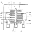
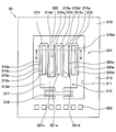
- the angular velocity sensor 30 includes a sensor unit 301 configured using a substrate 310 such as quartz or PZT (lead zirconate titanate) as a piezoelectric material.
- the substrate 310 is subjected to well-known micromachining to form a groove portion 311, and the groove portion 311 defines a vibrating body 312 and an outer peripheral portion 313.
- the vibrating body 312 In the vibrating body 312, the first drive piece 314, the second drive piece 315, and the detection piece 316 are held by the base portion 317, and the base portion 317 is fixed to the outer peripheral portion 313 via the beam portion 318. More specifically, the vibrating body 312 is a so-called tripod tuning fork type in which the first drive piece 314, the second drive piece 315, and the detection piece 316 are arranged so as to protrude from the base 317 in the same direction. Is disposed between the first drive piece 314 and the second drive piece 315.
- the beam part 318 relieves the stress which generate
- the first drive piece 314, the second drive piece 315, and the detection piece 316 are front surfaces 314 a, 315 a, 316 a, rear surfaces 314 b, 315 b, 316 b that are parallel to the surface direction of the substrate 310. , Side bars 314 c, 314 d, 315 c, 315 d, 316 c, and 316 d, and a bar shape having a rectangular cross section.
- a driving electrode 319a is formed on the front surface 314a
- a driving electrode 319b is formed on the back surface 314b
- common electrodes 319c and 319d are formed on the side surfaces 314c and 314d.
- the drive electrode 320a is formed on the front surface 315a
- the drive electrode 320b is formed on the back surface 315b
- the common electrodes 320c and 320d are formed on the side surfaces 315c and 315d.
- a detection electrode 321a is formed on the front surface 316a
- a detection electrode 321b is formed on the back surface 316b
- common electrodes 321c and 321d are formed on the side surfaces 316c and 316d.
- the second sensing unit 322 includes the first drive piece 314 and the second drive piece 315, the detection piece 316, the drive electrodes 319a to 320b, the detection electrodes 321a and 321b, and the common electrodes 319c to 321d. Has been.
- the outer peripheral portion 313 is electrically connected to the drive electrodes 319a to 320b, the detection electrodes 321a and 321b, and the common electrodes 319c to 321d via a wiring layer (not shown) and the circuit board 40.
- a plurality of pad portions 323 that are electrically connected to each other are formed.
- the second sensing unit 322 is not hermetically sealed in the hermetic chamber.
- the first drive piece 314 and the second drive piece 315 are vibrated in the arrangement direction of the first drive piece 314, the second drive piece 315, and the detection piece 316 (the left and right direction in FIG. 4). The angular velocity is detected in the state.
- the first drive piece 314 and the second drive piece 315 are along the protruding direction with respect to the base 317 of the first drive piece 314 and the second drive piece 315.
- a pair of Coriolis forces that are directions and opposite directions are periodically generated. For this reason, the moment generated by the Coriolis force is transmitted to the detection piece 316 via the base 317, so that the detection piece 316 vibrates in the arrangement direction of the first drive piece 314, the second drive piece 315, and the detection piece 316. (Bending), a charge corresponding to the angular velocity is generated in the detection piece 316. Therefore, a sensor signal corresponding to the angular velocity (charge) is output from the angular velocity sensor 30.
- the circuit board 40 includes an angular velocity sensor control circuit 410 that drives the angular velocity sensor 30, a self-diagnosis circuit 420, an acceleration sensor control circuit (not shown) that controls the acceleration sensor 20, and each sensor. It has a processing circuit (not shown) for processing signals.
- the detection piece 316 is omitted.
- the angular velocity sensor control circuit 410 includes a drive circuit 411, a charge amplifier 412, a rectifier circuit 413, a first reference voltage generation circuit 414, a differential amplifier 415, and the like.
- the self-diagnosis circuit 420 includes a low-pass filter 421, a second reference voltage generation circuit 422, an adder 423, a subtractor 424, a window comparator 425, and the like.
- the drive circuit 411 includes an AGC (Auto Gain Control) circuit and is connected to the drive electrodes 319a and 319b of the first drive piece 314 and the drive electrode 320b of the second drive piece 315. Then, a fixed drive signal whose amplification factor is adjusted based on the voltage signal input from the charge amplifier 412 and the difference signal 430 input from the differential amplifier 415 is applied to the drive electrodes 319a, 319b, and 320b. That is, the adjusted drive signal is applied to the drive electrodes 319a, 319b, and 320b so that the vibration amplitudes of the first drive piece 314 and the second drive piece 315 are constant.
- AGC Automatic Gain Control
- a pulsed drive signal (carrier wave) having a predetermined amplitude and frequency is applied to the drive electrodes 319a and 319b of the first drive piece 314.
- a drive signal (carrier wave) that is 180 ° out of phase with the drive signal (carrier wave) applied to the drive electrodes 319a and 319b is applied to the drive electrode 320b of the second drive piece 315. Accordingly, the first drive piece 314 and the second drive piece 315 vibrate in the arrangement direction of the first drive piece 314, the second drive piece 315, and the detection piece 316.
- the charge amplifier 412 is connected to the drive electrode 320a of the second drive piece 315 and is connected to the drive circuit 411 and the rectifier circuit 413. Then, the electric charge generated in the drive electrode 320a due to the vibration of the second drive piece 315 is converted into a voltage signal, and the voltage signal is input to the drive circuit 411 and the rectifier circuit 413.
- the electric charge generated at the drive electrode 320 a of the second drive piece 315 changes according to the vibration state of the second drive piece 315. That is, it changes according to the pressure (detection environment) around the second drive piece 315 (vibrating body 312).
- the rectifier circuit 413 is connected to the differential amplifier 415, generates a DC voltage corresponding to the vibration amplitude of the second drive piece 315 from the voltage signal input from the charge amplifier 412, and inputs the DC voltage to the differential amplifier 415.
- the first reference voltage generation circuit 414 is connected to the differential amplifier 415 and inputs the first reference voltage to the differential amplifier 415.
- the differential amplifier 415 is connected to the drive circuit 411, the low-pass filter 421, and the window comparator 425. Then, a difference signal 430 between the DC voltage input from the rectifier circuit 413 and the first reference voltage input from the first reference voltage generation circuit 414 is input to the drive circuit 411, the low-pass filter 421, and the window comparator 425.
- the difference signal 430 output from the differential amplifier 415 is also a signal according to the detection environment.
- the differential amplifier 415 corresponds to a detection unit, and the difference signal 430 corresponds to a detection signal.
- the low pass filter 421 has a large time constant and is connected to the adder 423 and the subtractor 424.
- the difference signal 430 When the difference signal 430 is input, an output signal that gently follows the difference signal 430 is generated, and the output signal is input to the adder 423 and the subtractor 424.
- the low-pass filter 421 basically generates an output having a voltage equivalent to that of the difference signal 430.
- the difference signal 430 fluctuates rapidly, the low-pass filter 421 can follow the signal so as to completely match it. Instead, an output signal that follows in a slightly delayed state is generated.
- a filter having a cutoff frequency of about 0.1 Hz or 0.01 Hz is used as the low-pass filter 421 in order to absorb temperature fluctuation and aging.
- the second reference voltage generation circuit 422 is connected to the adder 423 and the subtractor 424, generates a second reference voltage, and inputs the second reference voltage to the adder 423 and the subtractor 424. This second reference voltage determines the range of the determination threshold value in the window comparator 425.
- the adder 423 is connected to the window comparator 425, and inputs the upper reference voltage 431 obtained by adding the second reference voltage to the output of the low-pass filter 421 to the window comparator 425.
- the subtractor 424 is connected to the window comparator 425, and inputs the lower limit reference voltage 432 obtained by subtracting the second reference voltage from the output of the low-pass filter 421 to the window comparator 425.
- the window comparator 425 includes the voltage of the difference signal 430 between the normal voltage range defined by the upper limit reference voltage 431 input from the adder 423 and the lower limit reference voltage 432 input from the subtractor 424. Determine whether. Then, the window comparator 425 outputs a diagnosis detection signal Vout according to whether or not the voltage of the difference signal 430 is within the normal voltage range. For example, when the voltage of the difference signal 430 is within the normal voltage range, the window comparator 425 outputs a high-level voltage signal indicating that the diagnosis signal Vout is normal. Further, when the voltage of the difference signal 430 is not within the normal voltage range, a low level detection signal indicating that the diagnosis signal Vout is abnormal is output.
- the window comparator 425 corresponds to a self-diagnosis unit.
- the common electrodes 319c to 320d are connected to the ground potential.
- the voltage signal converted by the charge amplifier 412 changes, and the difference signal 430 output from the differential amplifier 415 changes. That is, the differential signal 430 corresponding to the detection environment of the vibrating body 312 is output from the differential amplifier 415.
- the difference signal 430 is input from the differential amplifier 415 to the window comparator 425, and it is determined whether or not the difference signal 430 is within the normal voltage range.
- the window comparator 425 outputs an abnormal voltage as the diagnosis detection signal Vout, and it is detected that the pressure in the accommodation space 15 has fluctuated. . That is, the detection environment of the angular velocity sensor 30 is self-diagnosed.
- the detection environment of the angular velocity sensor 30 is abnormal, a leak has occurred in the airtight chamber 255 of the acceleration sensor 20, so that the self-diagnosis can be made that the detection environment of the acceleration sensor 20 is also abnormal.
- the ratio of the volume of the hermetic chamber 255 to the volume of the accommodation space 15 is set to 1.0 ⁇ 10 ⁇ 7 or more. As shown in FIG. 8, when the ratio of the volume of the airtight chamber 255 to the volume of the storage space 15 is less than 1.0 ⁇ 10 ⁇ 7 , even if a leak occurs in the airtight chamber 255, This is because the pressure does not easily fluctuate.
- the vibration state of the first drive piece 314 and the second drive piece 315 is detected, and the difference signal 430 corresponding to the vibration state is output from the differential amplifier 415. That is, when a leak occurs in the hermetic chamber 255 and the pressure in the accommodation space 15 fluctuates, the vibration state of the first drive piece 314 and the second drive piece 315 changes, and therefore a difference corresponding to the pressure in the accommodation space 15. A signal 430 is output from the differential amplifier 415.
- the window comparator 425 determines whether the difference signal 430 is within the normal voltage range. For this reason, the self-diagnosis of the detection environment of the angular velocity sensor 30 (pressure in the accommodation space 15) can be performed. Further, when the detection environment of the angular velocity sensor 30 is abnormal, a leak has occurred in the airtight chamber 255 of the acceleration sensor 20, so that it can be self-diagnosed that the detection environment of the acceleration sensor 20 is also abnormal. Therefore, when various processes are performed using the signals output from the acceleration sensor 20 and the angular velocity sensor 30, it is possible to suppress erroneous processes.
- the acceleration sensor 20 is packaged, but the angular velocity sensor 30 may be packaged.
- the accommodation space 15 is set to atmospheric pressure, and the airtight chamber that seals the second sensing unit 322 of the angular velocity sensor 30 is set to a vacuum pressure.
- both the acceleration sensor 20 and the angular velocity sensor 30 may be packaged.
- the storage space 15 may be set to atmospheric pressure or a vacuum pressure.
- the angular velocity sensor 30 may not be a tripod tuning fork type.
- the angular velocity sensor 30 may be a so-called T-type tuning fork type in which the first drive piece 314, the second drive piece 315, and the detection piece 316 protrude from both sides with the base portion 317 interposed therebetween.
- the angular velocity sensor 30 may be a so-called H-type tuning fork, a normal tuning fork type, or the like.
- the angular velocity sensor 30 may be a capacitive type. That is, the configuration of the angular velocity sensor 30 is not particularly limited as long as the angular velocity is detected while vibrating the vibrating body 312.
- the acceleration sensor 20 may be a piezoelectric type.
Abstract
物理量センサは、角速度センサ(30)における振動体(312)の振動に応じた検出信号(430)を出力する検出部(415)と、検出部(415)から出力された検出信号(430)に基づき、加速度センサ(20)および角速度センサ(30)の検出環境を自己診断する自己診断部(425)を備える。
Description
本出願は、2014年6月12日に出願された日本出願番号2014-121690号に基づくもので、ここにその記載内容を援用する。
本開示は、加速度に応じたセンサ信号を出力するセンシング部が形成された加速度センサおよび角速度に応じたセンサ信号を出力するセンシング部が形成された角速度センサを共通のケースの収容空間に収容した物理量センサに関するものである。
従来より、加速度に応じたセンサ信号を出力するセンシング部が形成された加速度センサおよび角速度に応じたセンサ信号を出力するセンシング部が形成された角速度センサを共通のケースの収容空間に収容した物理量センサが記載されている(例えば、特許文献1参照)。
ここで、加速度センサは、加速度が印加されていない状態では静止状態であることが望まれるため、エアダンピング(気体の流動抵抗)が大きい大気圧下で加速度の検出を行うことが好ましい。これに対し、角速度センサは、振動体を有し、振動体を振動させている状態で角速度の検出を行う。このため、角速度センサは、振動体が振動し易いようにエアダンピングが小さい真空圧下で角速度の検出を行うことが好ましい。
したがって、共通のケースの収容空間に加速度センサおよび角速度センサを収容する場合には、例えば、収容空間の圧力が真空圧とされ、角速度センサがそのまま収容空間に配置される。また、加速度センサは、センシング部が大気圧とされた気密室に気密封止されたパッケージ構造の状態で収容空間に配置される。
しかしながら、上記物理量センサでは、パッケージ構造とされた加速度センサの気密室にリークが発生すると、収容空間の圧力および気密室の圧力が変動する。また、加速度センサは、気密室の圧力が変動した場合でも印加された加速度に応じたセンサ信号を出力する。同様に、角速度センサは、収容空間の圧力が変動した場合でも印加された角速度に応じたセンサ信号を出力する。つまり、検出環境が変動した場合には、検出精度が変化した状態のまま加速度および角速度の検出を行う。そして、上記物理量センサでは、検出環境を把握することができない。このため、加速度センサから出力されるセンサ信号および角速度センサから出力されるセンサ信号を用いて車両の走行制御等の各種の処理を行う場合、誤った処理を行ってしまう可能性がある。
本開示は上記点に鑑みて、加速度センサおよび角速度センサの検出環境を自己診断できる物理量センサを提供することを目的とする。
本開示の第一の態様において、物理量センサは、加速度に応じたセンサ信号を出力する第1センシング部が形成された加速度センサと、所定方向に振動する振動体を有する第2センシング部が形成され、センシング部から角速度に応じたセンサ信号が出力される角速度センサと、所定圧力とされた収容空間を有し、収容空間に加速度センサおよび角速度センサを収容するケースと、を備えている。加速度センサおよび角速度センサの少なくともいずれか一方は、センシング部が形成されたセンサ部にキャップ部が配置され、センシング部がセンサ部とキャップ部との間に構成される気密室に気密封止されたパッケージ構造である。
物理量センサは、角速度センサにおける振動体の振動に応じた検出信号を出力する検出部と、検出部から出力された検出信号に基づき、角速度センサの検出環境を自己診断する自己診断部と、を有している。
これによれば、自己診断部によって角速度センサの検出環境を自己診断できる。例えば、加速度センサのみがパッケージ構造とされ、収容空間の圧力が真空圧とされている物理量センサにおいて、パッケージ構造である加速度センサの気密室にリークが発生した場合には、収容空間の圧力(角速度センサの検出環境)が変動するため、振動体の振動状態が変化する。このため、検出信号に基づいて角速度センサの検出環境が異常であると判定できる。そして、角速度センサの検出環境が異常となるのはパッケージ構造である加速度センサの気密室にリークが発生した場合であるため、角速度センサが異常である場合には加速度センサの検出環境も異常であると判定できる。したがって、加速度センサおよび角速度センサから出力される信号を用いて各種の処理を行う場合、誤った処理を行うことを抑制できる。
本開示についての上記目的およびその他の目的、特徴や利点は、添付の図面を参照しながら下記の詳細な記述により、より明確になる。その図面は、
図1は、本開示の第1実施形態における物理量センサの断面図であり、
図2は、図1に示す加速度センサの断面図であり、
図3は、図2に示すセンサ部の平面図であり、
図4は、図1に示す角速度センサの平面図であり、
図5は、図4中のV-V線に沿った断面図であり、
図6は、図1に示す角速度センサと回路基板との回路構成を示す図であり、
図7は、圧力とインピーダンスとの関係を示す図であり、
図8は、気密室にリークが発生したときの収容空間の圧力と、収容空間の体積に対する気密室の体積の比との関係を示す図である。
以下、本開示の実施形態について図に基づいて説明する。なお、以下の各実施形態相互において、互いに同一もしくは均等である部分には、同一符号を付して説明を行う。
(第1実施形態)
本開示の第1実施形態について図面を参照しつつ説明する。図1に示されるように、物理量センサは、ケース10を備えており、当該ケース10は収容部11と蓋部12とを有する。
本開示の第1実施形態について図面を参照しつつ説明する。図1に示されるように、物理量センサは、ケース10を備えており、当該ケース10は収容部11と蓋部12とを有する。
収容部11は、アルミナ等のセラミック層が複数積層され、一面11aに第1凹部13が形成されると共に第1凹部13の底面に第2凹部14が形成されることによって収容空間15が構成される箱状とされている。そして、収容部11には、内壁面(第1凹部13の壁面、第2凹部14の壁面)に内部接続端子16a、16bが形成され、外壁面に図示しない外部接続端子が形成されている。これら内部接続端子16a、16bおよび外部接続端子は、内部に形成された図示しない内層配線等によって適宜電気的に接続されている。
蓋部12は、金属等で構成されており、収容部11の一面11aに溶接接合等されることにより、収容空間15を気密封止している。本実施形態では、収容空間15は真空圧とされ、例えば、1Paとされている。
そして、ケース10の収容空間15には、加速度センサ20、角速度センサ30および回路基板40がそれぞれ収容されている。具体的には、第2凹部14の底面に回路基板40が接着剤51を介して配置され、回路基板40の上に加速度センサ20が接着剤52を介して積層されている。そして、回路基板40は、内部接続端子16bとボンディングワイヤ61を介して電気的に接続され、加速度センサ20は回路基板40とボンディングワイヤ62を介して電気的に接続されている。
また、第1凹部13の底面に接着剤53を介して角速度センサ30が配置されている。詳述すると、角速度センサ30は、外周部313を有しており、外周部313が接着剤53と接合されている。そして、角速度センサ30は、内部接続端子16aとボンディングワイヤ63を介して電気的に接続されている。
なお、加速度センサ20は大気圧で封止されたパッケージ構造とされており、パッケージ状態で収容空間15に配置されている。また、角速度センサ30はそのまま収容空間15に配置されている。このため、加速度センサ20は大気圧下で加速度の検出を行い、角速度センサ30は真空圧下で角速度の検出を行う。
次に、加速度センサ20、角速度センサ30および回路基板40の構成についてそれぞれ説明する。
加速度センサ20は、図2に示されるように、センサ部201とキャップ部202とを備えたパッケージ構造とされている。
センサ部201は、支持基板211、絶縁膜212、半導体層213が順に積層されたSOI(Silicon on Insulator)基板214を用いて構成されている。なお、支持基板211および半導体層213はシリコン基板等で構成され、絶縁膜212は酸化膜等で構成される。
そして、SOI基板214には、図2および図3に示されるように、周知のマイクロマシン加工が施されて第1センシング部215が形成されている。具体的には、半導体層213には、溝部216が形成されることによって櫛歯形状の梁構造体を有する可動部220および第1固定部230と第2固定部240が形成されており、この梁構造体によって加速度に応じたセンサ信号を出力する第1センシング部215が形成されている。
また、絶縁膜212のうちの梁構造体220~240の形成領域に対応した部位には、犠牲層エッチング等によって矩形状に除去された開口部217が形成されている。
可動部220は、開口部217を横断するように配置されており、矩形状の錘部221における長手方向の両端が梁部222を介してアンカー部223a、223bに一体に連結した。アンカー部223a、223bは、開口部217の開口縁部で絶縁膜212を介して支持基板211に支持されている。これにより、錘部221および梁部222は、開口部217に臨んだ状態となっている。なお、図2中のセンサ部201は、図3中のII-II線に沿った断面図に相当している。
梁部222は、平行な2本の梁がその両端で連結された矩形枠状とされており、2本の梁の長手方向と直交する方向に変位するバネ機能を有している。具体的には、梁部222は、錘部221の長手方向に沿った方向の成分を含む加速度を受けたとき、錘部221を長手方向へ変位させると共に、加速度の消失に応じて元の状態に復元させる。したがって、このような梁部222を介して支持基板211に連結された錘部221は、加速度が印加されると梁部222の変位方向へ変位する。
また、可動部220は、錘部221の長手方向と直交した方向に、錘部221の両側面から互いに反対方向へ一体的に突出形成された複数個の可動電極224を備えている。図3では、可動電極224は、錘部221の左側および右側に各々4個ずつ突出して形成されており、開口部217に臨んだ状態となっている。また、各可動電極224は、錘部221および梁部222と一体的に形成されており、梁部222が変位することによって錘部221と共に錘部221の長手方向に変位可能となっている。
第1固定部230と第2固定部240は、開口部217の開口縁部のうちのアンカー部223a、223bが支持されていない対向辺部において、絶縁膜212を介して支持基板211に支持されている。すなわち、第1固定部230と第2固定部240は、可動部220を挟むように配置されている。図3では、第1固定部230が可動部220に対して紙面左側に配置され、第2固定部240が可動部220に対して紙面右側に配置されている。そして、第1固定部230と第2固定部240は互いに電気的に独立している。
また、第1固定部230と第2固定部240は、可動電極224の側面と所定の検出間隔を有するように平行した状態で対向配置された複数個の第1固定電極231と第2固定電極241と、絶縁膜212を介して支持基板211に支持された第1配線部232と第2配線部242とを有している。
第1固定電極231と第2固定電極241は、図3では4個ずつ形成されており、可動電極224における櫛歯の隙間に噛み合うように櫛歯状に配列されている。そして、各配線部232と242に片持ち状に支持されることにより、開口部217に臨んだ状態となっている。以上が本実施形態におけるセンサ部201の構成である。
キャップ部202は、図2に示されるように、シリコン等の基板251のうちのセンサ部201と対向する一面側に絶縁膜252が形成されていると共に、この一面と反対側の他面に絶縁膜253が形成された。
そして、このキャップ部202は、絶縁膜252がセンサ部201(半導体層213)と接合されている。本実施形態では、絶縁膜252とセンサ部201(半導体層213)とは、絶縁膜252および半導体層213のうちの接合面を活性化させて接合するいわゆる直接接合等で接合されている。
また、キャップ部202には、第1センシング部215と対向する部分に窪み部254が形成されている。そして、センサ部201とキャップ部202との間には、この窪み部254を含む空間にて気密室255が構成され、センサ部201に形成された第1センシング部215が気密室255に気密封止されている。なお、本実施形態では、気密室255は大気圧とされている。つまり、本実施形態では、加速度センサ20は、第1センシング部215が大気圧とされた気密室255に気密封止されたパッケージ構造とされている。
また、キャップ部202には、当該キャップ部202とセンサ部201との積層方向に貫通する複数の貫通孔256(図2中では1つのみ図示)が形成されている。具体的には、この貫通孔256は、アンカー部223bおよび第1配線部232と第2配線部242の所定箇所を露出させるように形成されている。そして、貫通孔256の壁面には、TEOS(Tetraethyl orthosilicate)等で構成される絶縁膜257が成膜され、絶縁膜257の上にはAl等で構成される貫通電極258が適宜アンカー部223bおよび第1配線部232と第2配線部242と電気的に接続されるように形成されている。また、絶縁膜253の上には、回路基板40と電気的に接続されるパッド部259が形成されている。
そして、絶縁膜253、貫通電極258、パッド部259の上には、保護膜260が形成されており、保護膜260にはパッド部259を露出させるコンタクトホール260aが形成されている。
以上が加速度センサ20の構成である。このような加速度センサ20では、加速度が印加されると、錘部221が加速度に応じて変位することにより、可動電極224と第1固定電極231と第2固定電極241との間の容量が変化する。このため、加速度センサ20から加速度(容量)に応じたセンサ信号が出力される。
次に、角速度センサ30の構成について説明する。角速度センサ30は、図4に示されるように、圧電材料としての水晶やPZT(チタン酸ジルコン鉛)等の基板310を用いて構成されるセンサ部301を備えている。そして、基板310には、周知のマイクロマシン加工が施されて溝部311が形成され、溝部311によって振動体312および外周部313が区画形成されている。
振動体312は、第1駆動片314と第2駆動片315および検出片316が基部317に保持され、当該基部317が梁部318を介して外周部313に固定された。詳述すると、振動体312は、第1駆動片314と第2駆動片315および検出片316が基部317から同じ方向に突出するように配置されたいわゆる三脚音叉型とされており、検出片316が第1駆動片314と第2駆動片315の間に配置されている。
なお、梁部318は、外周部313に発生する応力を緩和して当該応力が振動体312に伝達されることを抑制するものであるが、備えられていなくてもよい。つまり、基部317がそのまま外周部313と連結されていてもよい。
第1駆動片314と第2駆動片315および検出片316は、図4および図5に示されるように、基板310の面方向と平行となる表面314a、315a、316a、裏面314b、315b、316b、側面314c、314d、315c、315d、316c、316dを有する断面矩形状とされた棒状とされている。
そして、第1駆動片314には、表面314aに駆動電極319aが形成されていると共に裏面314bに駆動電極319bが形成され、側面314c、314dに共通電極319c、319dが形成されている。同様に、第2駆動片315には、表面315aに駆動電極320aが形成されていると共に裏面315bに駆動電極320bが形成され、側面315c、315dに共通電極320c、320dが形成されている。また、検出片316には、表面316aに検出電極321aが形成されていると共に裏面316bに検出電極321bが形成され、側面316c、316dに共通電極321c、321dが形成されている。
なお、本実施形態では、第1駆動片314と第2駆動片315、検出片316、駆動電極319a~320b、検出電極321a、321b、共通電極319c~321dを含んで第2センシング部322が構成されている。
外周部313には、図4に示されるように、駆動電極319a~320b、検出電極321a、321b、共通電極319c~321dと図示しない配線層等を介して電気的に接続されると共に回路基板40と電気的に接続される複数のパッド部323が形成されている。
以上が角速度センサ30の構成である。つまり、本実施形態の角速度センサ30は、第2センシング部322が気密室に気密封止されていない。このような角速度センサ30では、第1駆動片314と第2駆動片315を第1駆動片314と第2駆動片315および検出片316の配列方向(図4中紙面左右方向)に振動させた状態で角速度の検出を行う。
そして、センサ部301の面内で角速度が印加されると、第1駆動片314と第2駆動片315には、第1駆動片314と第2駆動片315の基部317に対する突出方向に沿った方向であり、向きが反対の一対のコリオリ力が周期的に発生する。このため、コリオリ力によって発生するモーメントが基部317を介して検出片316に伝達されることにより、検出片316が第1駆動片314と第2駆動片315および検出片316の配列方向に振動し(撓み)、検出片316に角速度に応じた電荷が発生する。したがって、角速度センサ30から角速度(電荷)に応じたセンサ信号が出力される。
なお、角速度が印加されない場合には、第1駆動片314と第2駆動片315から基部317を介して検出片316に印加されるモーメントは逆方向であって相殺されるため、検出片316はほぼ静止した状態となる。
次に、回路基板40の回路構成について説明する。回路基板40は、図6に示されるように、角速度センサ30を駆動する角速度センサ用制御回路410、自己診断回路420、加速度センサ20を制御する加速度センサ用制御回路(図示せず)、各センサ信号を処理する処理回路(図示せず)等を有するものである。なお、図6では、検出片316を省略して示している。
角速度センサ用制御回路410は、駆動回路411、チャージアンプ412、整流回路413、第1基準電圧発生回路414、差動増幅器415等を有している。自己診断回路420は、ローパスフィルタ421、第2基準電圧発生回路422、加算器423、減算器424、ウィンドウコンパレータ425等を有している。
駆動回路411は、AGC(Auto Gain Control)回路等を有するものであり、第1駆動片314の駆動電極319a、319bおよび第2駆動片315の駆動電極320bと接続されている。そして、チャージアンプ412から入力される電圧信号および差動増幅器415から入力される差信号430に基づいて増幅率を調整した一定の駆動信号を駆動電極319a、319b、320bに印加する。つまり、第1駆動片314と第2駆動片315の振動振幅が一定となるように、調整した駆動信号を駆動電極319a、319b、320bに印加する。
なお、第1駆動片314の駆動電極319a、319bには、所定の振幅、周波数を有するパルス状の駆動信号(搬送波)が印加される。また、第2駆動片315の駆動電極320bには、駆動電極319a、319bに印加される駆動信号(搬送波)と位相が180°異なる駆動信号(搬送波)が印加される。これにより、第1駆動片314と第2駆動片315が第1駆動片314と第2駆動片315および検出片316の配列方向に振動する。
チャージアンプ412は、第2駆動片315の駆動電極320aに接続されていると共に、駆動回路411および整流回路413に接続されている。そして、第2駆動片315が振動することによって駆動電極320aに発生した電荷を電圧信号に変換し、当該電圧信号を駆動回路411および整流回路413に入力する。
なお、第2駆動片315の駆動電極320aに発生する電荷は、第2駆動片315の振動状態に応じて変化する。つまり、第2駆動片315(振動体312)の周囲の圧力(検出環境)に応じて変化する。
整流回路413は、差動増幅器415に接続されており、チャージアンプ412から入力された電圧信号から第2駆動片315の振動振幅に相当するDC電圧を生成して差動増幅器415に入力する。
第1基準電圧発生回路414は、差動増幅器415に接続されており、第1基準電圧を差動増幅器415に入力する。
差動増幅器415は、駆動回路411、ローパスフィルタ421、ウィンドウコンパレータ425に接続されている。そして、整流回路413から入力されたDC電圧と、第1基準電圧発生回路414から入力された第1基準電圧との差信号430を駆動回路411、ローパスフィルタ421、ウィンドウコンパレータ425に入力する。
なお、上記のように、第2駆動片315は検出環境に応じた電荷を発生するため、差動増幅器415から出力される差信号430も検出環境に応じた信号となる。このため、本実施形態では、差動増幅器415が検出部に相当し、差信号430が検出信号に相当している。
ローパスフィルタ421は、大きな時定数を有するものであり、加算器423および減算器424と接続されている。そして、差信号430が入力されると、当該差信号430に対して緩やかに追従する出力信号を発生し、当該出力信号を加算器423および減算器424に入力する。つまり、ローパスフィルタ421は、基本的には差信号430と同等の電圧を有する出力を発生させるが、差信号430が急激に変動する場合には、それに対して完全に一致するようには追従せずに、若干遅れた状態で追従する出力信号を発生させる。具体的には、ローパスフィルタ421としては、温度変動や経年変化を吸収するために、0.1Hzや0.01Hz程度のカットオフ周波数を持つものが用いられる。
第2基準電圧発生回路422は、加算器423および減算器424と接続されており、第2基準電圧を発生して当該第2基準電圧を加算器423および減算器424に入力する。この第2基準電圧は、ウィンドウコンパレータ425での判定閾値の範囲を決定するものである。
加算器423は、ウィンドウコンパレータ425と接続されており、ローパスフィルタ421の出力に対して第2基準電圧を加算した上限基準電圧431をウィンドウコンパレータ425に入力する。
減算器424は、ウィンドウコンパレータ425と接続されており、ローパスフィルタ421の出力に対して第2基準電圧を減算した下限基準電圧432をウィンドウコンパレータ425に入力する。
ウィンドウコンパレータ425は、加算器423から入力される上限基準電圧431と減算器424から入力される下限基準電圧432とによって規定される正常電圧範囲の間に差信号430の電圧が含まれているか否かを判定する。そして、ウィンドウコンパレータ425は、差信号430の電圧が正常電圧範囲の間に入っているか否かに応じたダイアグ検出信号Voutを出力する。例えば、ウィンドウコンパレータ425は、差信号430の電圧が正常電圧範囲内である場合には、ダイアグ検出信号Voutとして正常であることを意味するハイレベルの電圧信号を出力する。また、差信号430の電圧が正常電圧範囲内でない場合には、ダイアグ検出信号Voutとして異常であることを意味するローレベルの検出信号を出力する。
なお、ここでの正常であるとは、第1駆動片314と第2駆動片315が所望の振動をしていることであり、異常であるとは、第1駆動片314と第2駆動片315が所望の振動をしていないことである。そして、本実施形態では、ウィンドウコンパレータ425が自己診断部に相当している。また、共通電極319c~320dは、グランド電位と接続されている。
以上が本実施形態における物理量センサの構成である。次に、上記物理量センサの自己診断について説明する。
このような物理量センサでは、加速度センサ20における気密室255にリークが発生すると、収容空間15の圧力(真空度)が高くなる。このため、図7に示されるように、第1駆動片314と第2駆動片315のインピーダンスが大きくなり、第1駆動片314と第2駆動片315の振動が小さくなる。言い換えると、第1駆動片314と第2駆動片315が正常に振動しなくなる。そして、第1駆動片314と第2駆動片315の振動が小さくなるため、第2駆動片314の駆動電極320aに発生する電荷も小さくなる。
したがって、チャージアンプ412で変換される電圧信号が変化し、差動増幅器415から出力される差信号430が変化する。つまり、差動増幅器415から振動体312の検出環境に応じた差信号430が出力される。
次に、上記のように、差動増幅器415から差信号430がウィンドウコンパレータ425に入力され、差信号430が正常電圧範囲内であるか否かが判定される。そして、差信号430が正常電圧範囲内にない場合には、ウィンドウコンパレータ425からダイアグ検出信号Voutとして異常であることを意味する電圧が出力され、収容空間15の圧力が変動したことが検出される。つまり、角速度センサ30の検出環境が自己診断される。
そして、角速度センサ30の検出環境が異常である場合は、加速度センサ20における気密室255にリークが発生しているため、加速度センサ20の検出環境も異常であると自己診断できる。
ここで、本実施形態では、収容空間15の体積に対する気密室255の体積の比が1.0×10⁻⁷以上とされている。図8に示されるように、収容空間15の体積に対する気密室255の体積の比が1.0×10⁻⁷未満とされていると、気密室255にリークが発生しても収容空間15の圧力が変動し難いためである。
以上説明したように、本実施形態では、第1駆動片314と第2駆動片315の振動状態を検出し、振動状態に応じた差信号430が差動増幅器415から出力される。つまり、気密室255にリークが発生して収容空間15の圧力が変動した場合には第1駆動片314と第2駆動片315の振動状態が変化するため、収容空間15の圧力に応じた差信号430が差動増幅器415から出力される。
そして、ウィンドウコンパレータ425において、差信号430が正常電圧範囲内であるか否かを判定している。このため、角速度センサ30の検出環境(収容空間15の圧力)を自己診断できる。また、角速度センサ30の検出環境が異常である場合は、加速度センサ20における気密室255にリークが発生しているため、加速度センサ20の検出環境も異常であると自己診断できる。したがって、加速度センサ20および角速度センサ30から出力される信号を用いて各種の処理を行う場合、誤った処理を行うことを抑制できる。
(他の実施形態)
本開示は上記した実施形態に限定されるものではなく、特許請求の範囲に記載した範囲内において適宜変更が可能である。
本開示は上記した実施形態に限定されるものではなく、特許請求の範囲に記載した範囲内において適宜変更が可能である。
例えば、上記第1実施形態では、加速度センサ20がパッケージ化されたものを説明したが、角速度センサ30がパッケージ化されていてもよい。この場合、収容空間15が大気圧とされ、角速度センサ30の第2センシング部322を封止する気密室が真空圧とされる。また、加速度センサ20および角速度センサ30が共にパッケージ化されていてもよい。この場合、収容空間15は大気圧とされていてもよいし、真空圧とされていてもよい。
また、上記第1実施形態において、角速度センサ30は、三脚音叉型でなくてもよい。例えば、角速度センサ30は、第1駆動片314と第2駆動片315および検出片316がそれぞれ基部317を挟んで両側に突出したいわゆるT型音叉型とされていてもよい。また、角速度センサ30は、いわゆるH型音叉や通常の音叉型等とされていてもよい。さらに、角速度センサ30は、容量型であってもよい。つまり、振動体312を振動させながら角速度の検出を行うものであれば、角速度センサ30の構成は特に限定されるものではない。
そして、上記第1実施形態において、加速度センサ20は、圧電型であってもよい。
本開示は、実施例に準拠して記述されたが、本開示は当該実施例や構造に限定されるものではないと理解される。本開示は、様々な変形例や均等範囲内の変形をも包含する。加えて、様々な組み合わせや形態、さらには、それらに一要素のみ、それ以上、あるいはそれ以下、を含む他の組み合わせや形態をも、本開示の範疇や思想範囲に入るものである。
Claims (5)
- 加速度に応じたセンサ信号を出力するセンシング部(215)が形成された加速度センサ(20)と、
所定方向に振動する振動体(312)を有するセンシング部(322)が形成され、前記センシング部から角速度に応じたセンサ信号が出力される角速度センサ(30)と、
所定圧力とされた収容空間(15)を有し、前記収容空間に前記加速度センサおよび前記角速度センサを収容するケース(10)と、を備え、
前記加速度センサおよび前記角速度センサの少なくともいずれか一方は、前記センシング部が形成されたセンサ部(201)にキャップ部(202)が配置され、前記センシング部が前記センサ部と前記キャップ部との間に構成される気密室(255)に気密封止されたパッケージ構造であり、
前記角速度センサにおける振動体の振動に応じた検出信号(430)を出力する検出部(415)と、
前記検出部から出力された検出信号に基づき、前記角速度センサの検出環境を自己診断する自己診断部(425)と、を有している物理量センサ。 - 前記収容空間の体積に対する前記気密室の体積の比は、1.0×10⁻⁷以上とされている請求項1に記載の物理量センサ。
- 前記加速度センサは、前記パッケージ構造とされ、前記気密室が大気圧とされており、
前記収容空間は、真空圧とされている請求項1または2に記載の物理量センサ。 - 前記角速度センサは、前記パッケージ構造とされ、前記気密室が真空圧とされており、
前記収容空間は、大気圧とされている請求項1または2に記載の物理量センサ。 - 前記角速度センサは、前記パッケージ構造とされ、前記気密室が真空圧とされており、
前記加速度センサは、前記パッケージ構造とされ、前記気密室が大気圧とされている請求項1または2に記載の物理量センサ。
Priority Applications (2)
| Application Number | Priority Date | Filing Date | Title |
|---|---|---|---|
| US15/307,859 US10393523B2 (en) | 2014-06-12 | 2015-06-11 | Physical quantity sensor |
| DE112015002785.8T DE112015002785T5 (de) | 2014-06-12 | 2015-06-11 | Sensor für eine physikalische Grösse |
Applications Claiming Priority (2)
| Application Number | Priority Date | Filing Date | Title |
|---|---|---|---|
| JP2014-121690 | 2014-06-12 | ||
| JP2014121690A JP6409351B2 (ja) | 2014-06-12 | 2014-06-12 | 物理量センサ |
Publications (1)
| Publication Number | Publication Date |
|---|---|
| WO2015190104A1 true WO2015190104A1 (ja) | 2015-12-17 |
Family
ID=54833215
Family Applications (1)
| Application Number | Title | Priority Date | Filing Date |
|---|---|---|---|
| PCT/JP2015/002919 WO2015190104A1 (ja) | 2014-06-12 | 2015-06-11 | 物理量センサ |
Country Status (4)
| Country | Link |
|---|---|
| US (1) | US10393523B2 (ja) |
| JP (1) | JP6409351B2 (ja) |
| DE (1) | DE112015002785T5 (ja) |
| WO (1) | WO2015190104A1 (ja) |
Families Citing this family (4)
| Publication number | Priority date | Publication date | Assignee | Title |
|---|---|---|---|---|
| JP6586735B2 (ja) * | 2015-02-20 | 2019-10-09 | セイコーエプソン株式会社 | 回路装置、物理量検出装置、電子機器及び移動体 |
| JP6492739B2 (ja) | 2015-02-20 | 2019-04-03 | セイコーエプソン株式会社 | 回路装置、物理量検出装置、電子機器及び移動体 |
| KR102437764B1 (ko) | 2017-12-20 | 2022-08-30 | 삼성전자주식회사 | 센서 패키지, 센서 패키지의 제조 방법, 및 리드 구조체의 제조 방법 |
| JP6996344B2 (ja) * | 2018-02-28 | 2022-01-17 | セイコーエプソン株式会社 | センサーデバイス、力検出装置およびロボット |
Citations (4)
| Publication number | Priority date | Publication date | Assignee | Title |
|---|---|---|---|---|
| JPH10206273A (ja) * | 1997-01-21 | 1998-08-07 | Toyota Motor Corp | 角速度センサの気密性確認方法及び装置 |
| JP2011017693A (ja) * | 2009-06-09 | 2011-01-27 | Denso Corp | 半導体力学量センサの製造方法及び半導体力学量センサ |
| JP2011179821A (ja) * | 2010-02-26 | 2011-09-15 | Hitachi Automotive Systems Ltd | 複合センサの製造方法 |
| JP2013120179A (ja) * | 2011-12-09 | 2013-06-17 | Panasonic Corp | 角速度センサ |
Family Cites Families (17)
| Publication number | Priority date | Publication date | Assignee | Title |
|---|---|---|---|---|
| JP3123352B2 (ja) | 1994-06-29 | 2001-01-09 | 株式会社デンソー | 漏れ測定方法及びその装置 |
| JPH1151802A (ja) * | 1997-07-31 | 1999-02-26 | River Eletec Kk | 圧電素子用パッケージの気密検査方法 |
| JP3435665B2 (ja) | 2000-06-23 | 2003-08-11 | 株式会社村田製作所 | 複合センサ素子およびその製造方法 |
| JP3512004B2 (ja) | 2000-12-20 | 2004-03-29 | トヨタ自動車株式会社 | 力学量検出装置 |
| DE102004027501A1 (de) | 2004-06-04 | 2005-12-22 | Robert Bosch Gmbh | Mikromechanisches Bauelement mit mehreren Kavernen und Herstellungsverfahren |
| JP2006010659A (ja) | 2004-06-21 | 2006-01-12 | Microstone Corp | 振動ジャイロスコープ |
| JP4543869B2 (ja) | 2004-10-15 | 2010-09-15 | 株式会社デンソー | 振動型角速度センサにおけるセンサ回路 |
| JP5222457B2 (ja) * | 2005-09-26 | 2013-06-26 | 株式会社日立製作所 | センサおよびセンサモジュール |
| DE102006016260A1 (de) | 2006-04-06 | 2007-10-18 | Fraunhofer-Gesellschaft zur Förderung der angewandten Forschung e.V. | Mikromechanische Gehäusung mit mindestens zwei Kavitäten mit unterschiedlichem Innendruck und/oder unterschiedlicher Gaszusammensetzung sowie Verfahren zu deren Herstellung |
| CN101796374A (zh) * | 2007-09-03 | 2010-08-04 | 松下电器产业株式会社 | 惯性力传感器 |
| JP5319122B2 (ja) | 2008-01-21 | 2013-10-16 | 日立オートモティブシステムズ株式会社 | 慣性センサ |
| US7800190B2 (en) * | 2008-06-16 | 2010-09-21 | Honeywell International Inc. | Getter on die in an upper sense plate designed system |
| JP5321150B2 (ja) | 2009-03-05 | 2013-10-23 | セイコーエプソン株式会社 | 複合センサー |
| JP2010204061A (ja) * | 2009-03-06 | 2010-09-16 | Panasonic Corp | 電子部品及びその製造方法 |
| US20120142136A1 (en) | 2010-12-01 | 2012-06-07 | Honeywell International Inc. | Wafer level packaging process for mems devices |
| WO2013080238A1 (ja) * | 2011-11-28 | 2013-06-06 | 日立オートモティブシステムズ株式会社 | 複合センサおよびその製造方法 |
| JP6435631B2 (ja) | 2014-04-23 | 2018-12-12 | 株式会社デンソー | 角速度センサ |
-
2014
- 2014-06-12 JP JP2014121690A patent/JP6409351B2/ja active Active
-
2015
- 2015-06-11 US US15/307,859 patent/US10393523B2/en active Active
- 2015-06-11 WO PCT/JP2015/002919 patent/WO2015190104A1/ja active Application Filing
- 2015-06-11 DE DE112015002785.8T patent/DE112015002785T5/de active Pending
Patent Citations (4)
| Publication number | Priority date | Publication date | Assignee | Title |
|---|---|---|---|---|
| JPH10206273A (ja) * | 1997-01-21 | 1998-08-07 | Toyota Motor Corp | 角速度センサの気密性確認方法及び装置 |
| JP2011017693A (ja) * | 2009-06-09 | 2011-01-27 | Denso Corp | 半導体力学量センサの製造方法及び半導体力学量センサ |
| JP2011179821A (ja) * | 2010-02-26 | 2011-09-15 | Hitachi Automotive Systems Ltd | 複合センサの製造方法 |
| JP2013120179A (ja) * | 2011-12-09 | 2013-06-17 | Panasonic Corp | 角速度センサ |
Also Published As
| Publication number | Publication date |
|---|---|
| US20170059320A1 (en) | 2017-03-02 |
| US10393523B2 (en) | 2019-08-27 |
| JP2016001158A (ja) | 2016-01-07 |
| DE112015002785T5 (de) | 2017-03-02 |
| JP6409351B2 (ja) | 2018-10-24 |
Similar Documents
| Publication | Publication Date | Title |
|---|---|---|
| US9835641B2 (en) | Angular velocity detection device and angular velocity sensor including the same | |
| JP6160027B2 (ja) | 振動片およびジャイロセンサー並びに電子機器および移動体 | |
| US10119821B2 (en) | Angular velocity sensor | |
| JP6897187B2 (ja) | 物理量検出器、物理量検出デバイス、電子機器および移動体 | |
| WO2015190105A1 (ja) | 物理量センサ | |
| WO2015190104A1 (ja) | 物理量センサ | |
| JP4599848B2 (ja) | 角速度センサ | |
| WO2016113828A1 (ja) | 複合センサ | |
| CN103105261A (zh) | 物理量检测器 | |
| JP6435631B2 (ja) | 角速度センサ | |
| JP4974359B2 (ja) | 力学量センサ | |
| JP2008275325A (ja) | センサ装置 | |
| WO2017033717A1 (ja) | 複合センサ | |
| JP4869001B2 (ja) | 振動ジャイロ | |
| JP2006226799A (ja) | 力学量センサ | |
| JPH0989569A (ja) | 振動ジャイロ | |
| JP4333474B2 (ja) | 圧電振動子 | |
| JP4600590B2 (ja) | 角速度センサ | |
| WO2014030492A1 (ja) | 慣性力センサ | |
| JP5776184B2 (ja) | センサ装置 | |
| JP5321812B2 (ja) | 物理量センサーおよび物理量測定装置 | |
| JP2017122678A (ja) | 物理量センサ | |
| JP2011013063A (ja) | 圧力センサー及び圧力センサーの圧力検出方法 | |
| JP2012163386A (ja) | 角速度センサユニットおよびその信号検出方法 |
Legal Events
| Date | Code | Title | Description |
|---|---|---|---|
| 121 | Ep: the epo has been informed by wipo that ep was designated in this application |
Ref document number: 15806460 Country of ref document: EP Kind code of ref document: A1 |
|
| WWE | Wipo information: entry into national phase |
Ref document number: 15307859 Country of ref document: US |
|
| WWE | Wipo information: entry into national phase |
Ref document number: 112015002785 Country of ref document: DE |
|
| 122 | Ep: pct application non-entry in european phase |
Ref document number: 15806460 Country of ref document: EP Kind code of ref document: A1 |