WO2015182234A1 - 半導体装置およびその製造方法 - Google Patents
半導体装置およびその製造方法 Download PDFInfo
- Publication number
- WO2015182234A1 WO2015182234A1 PCT/JP2015/059725 JP2015059725W WO2015182234A1 WO 2015182234 A1 WO2015182234 A1 WO 2015182234A1 JP 2015059725 W JP2015059725 W JP 2015059725W WO 2015182234 A1 WO2015182234 A1 WO 2015182234A1
- Authority
- WO
- WIPO (PCT)
- Prior art keywords
- electrode layer
- protective film
- electrode
- layer
- semiconductor device
- Prior art date
- Legal status (The legal status is an assumption and is not a legal conclusion. Google has not performed a legal analysis and makes no representation as to the accuracy of the status listed.)
- Ceased
Links
Images






Classifications
-
- H—ELECTRICITY
- H10—SEMICONDUCTOR DEVICES; ELECTRIC SOLID-STATE DEVICES NOT OTHERWISE PROVIDED FOR
- H10P—GENERIC PROCESSES OR APPARATUS FOR THE MANUFACTURE OR TREATMENT OF DEVICES COVERED BY CLASS H10
- H10P14/00—Formation of materials, e.g. in the shape of layers or pillars
- H10P14/40—Formation of materials, e.g. in the shape of layers or pillars of conductive or resistive materials
-
- H—ELECTRICITY
- H10—SEMICONDUCTOR DEVICES; ELECTRIC SOLID-STATE DEVICES NOT OTHERWISE PROVIDED FOR
- H10W—GENERIC PACKAGES, INTERCONNECTIONS, CONNECTORS OR OTHER CONSTRUCTIONAL DETAILS OF DEVICES COVERED BY CLASS H10
- H10W20/00—Interconnections in chips, wafers or substrates
- H10W20/01—Manufacture or treatment
-
- H—ELECTRICITY
- H10—SEMICONDUCTOR DEVICES; ELECTRIC SOLID-STATE DEVICES NOT OTHERWISE PROVIDED FOR
- H10W—GENERIC PACKAGES, INTERCONNECTIONS, CONNECTORS OR OTHER CONSTRUCTIONAL DETAILS OF DEVICES COVERED BY CLASS H10
- H10W20/00—Interconnections in chips, wafers or substrates
- H10W20/40—Interconnections external to wafers or substrates, e.g. back-end-of-line [BEOL] metallisations or vias connecting to gate electrodes
Definitions
- the technology disclosed in this specification relates to a semiconductor device and a manufacturing method thereof.
- Patent Document 1 Japanese Unexamined Patent Publication No. 2010-272711 discloses a semiconductor device.
- the semiconductor device of Patent Document 1 includes a semiconductor substrate, a main electrode formed on the semiconductor substrate, and an additional electrode formed on the main electrode.
- the semiconductor substrate and the main electrode are covered with a passivation film.
- the additional electrode is soldered to the lead frame.
- gas may be generated from the passivation film by heating.
- gas may be generated from the passivation film when soldering.
- the electrode When the generated gas enters under the electrode, the electrode may be deformed, causing a problem in the semiconductor device.
- a semiconductor device disclosed in this specification includes a semiconductor substrate, a plurality of first electrode layers formed on the semiconductor substrate at intervals, and a gap between the adjacent first electrode layer and the first electrode layer. And a wiring formed on the substrate.
- the semiconductor device is formed on each of the adjacent first electrode layer and the insulating protective film that covers the semiconductor substrate and the wiring between the first electrode layer and the plurality of first electrode layers.
- a plurality of second electrode layers covers an end portion of the protective film, and the protective film is exposed between the adjacent second electrode layer and the second electrode layer.
- the protective film covers the wiring formed between the first electrode layer and the first electrode layer, the wiring can be protected.
- gas may be generated from the protective film by heating.
- gas may be generated from the protective film when soldering to the second electrode layer.
- the protective film since the protective film is exposed between the second electrode layer and the second electrode layer, the gas generated from the exposed portion is released to the outside. Thereby, gas does not enter between the protective film and the second electrode layer, and the second electrode layer can be prevented from being swollen and deformed by the gas.
- a method for manufacturing a semiconductor device disclosed in this specification includes a step of forming a plurality of first electrode layers on a semiconductor substrate at intervals, and a gap between the adjacent first electrode layer and the first electrode layer. Forming a wiring.
- a method for manufacturing a semiconductor device includes a step of forming an insulating protective film that covers the semiconductor substrate and the wiring between the adjacent first electrode layer and the first electrode layer; Forming a second electrode layer on each of the first electrode layer, the second electrode layer covering an end portion of the protective film, and the protective film from between the adjacent second electrode layer and the second electrode layer; Forming the second electrode layer so as to be exposed.
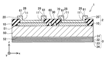
- FIG. 2 is a cross-sectional view taken along the line II-II in FIG. It is sectional drawing of a 2nd electrode layer.
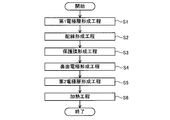
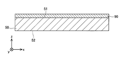
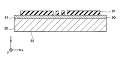
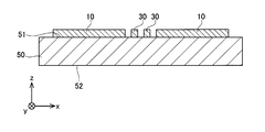
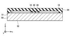
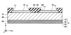
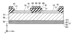
- It is a flowchart of the manufacturing method of a semiconductor device. It is sectional drawing for demonstrating the manufacturing method of a semiconductor device (1). It is sectional drawing for demonstrating the manufacturing method of a semiconductor device (2). It is sectional drawing for demonstrating the manufacturing method of a semiconductor device (3). It is sectional drawing for demonstrating the manufacturing method of a semiconductor device (4). It is sectional drawing for demonstrating the manufacturing method of a semiconductor device (5). It is sectional drawing for demonstrating the manufacturing method of a semiconductor device (6).
- the protective film may be formed of a resin.
- the protective film may be made of polyimide.
- the protective film may cover the end of the first electrode layer.
- the method includes a step of heating the protective film in a state where the protective film is exposed between the adjacent second electrode layer and the second electrode layer. May be.
- the step of heating the protective film may be performed when soldering.
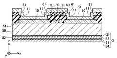
- the semiconductor device 1 includes a semiconductor substrate 50, a plurality of first electrode layers 10 (main electrodes) formed on the semiconductor substrate 50, and a first electrode layer. 10 and a second electrode layer 20 (additional electrode) respectively formed on the substrate 10.
- the semiconductor device 1 also includes a wiring 30 formed on the semiconductor substrate 50 and a protective film 60 that covers the semiconductor substrate 50 and the wiring 30.
- the semiconductor device 1 is not particularly limited.
- an RC-IGBT Reverse-Conducting-Insulated-Gate-Bipolar
- IGBT Insulated Gate-Bipolar-Transistor
- FWD Free Wheeling-Diode
- the semiconductor substrate 50 is formed to have a substantially rectangular shape in plan view.
- the semiconductor substrate 50 is formed of silicon (Si).
- the semiconductor substrate 50 may be formed of silicon carbide (SiC), gallium nitride (GaN), or the like.
- a semiconductor element (not shown) is formed inside the semiconductor substrate 50.
- a gate electrode, an emitter region, a collector region, and the like are formed inside the semiconductor substrate 50 (not shown).
- FWD an anode region, a cathode region, and the like are formed inside the semiconductor substrate 50 (not shown).
- the semiconductor substrate 50 has a front surface 51 and a back surface 52.
- a plurality of first electrode layers 10 are formed on the surface 51 of the semiconductor substrate 50.
- a second electrode layer 20 is formed on each of the plurality of first electrode layers 10.
- the surface electrode 2 is formed by the first electrode layer 10 and the second electrode layer 20.
- a plurality of signal electrodes 80 are formed on the surface 51 of the semiconductor substrate 50.
- a back electrode 3 is formed on the back surface 52 of the semiconductor substrate 50.
- the first electrode layer 10 is made of metal and has conductivity.
- a material of the first electrode layer 10 for example, an alloy containing aluminum (Al) as a main component can be used.
- Al aluminum
- AlSi aluminum silicon
- the plurality of first electrode layers 10 are formed side by side at intervals. In the present embodiment, two first electrode layers 10 are formed. The plurality of first electrode layers 10 are formed adjacent to each other.
- the wiring 30 is made of metal and has conductivity.
- a material of the wiring 30 for example, an alloy containing aluminum (Al) as a main component can be used.
- AlSi aluminum silicon
- the wiring 30 is formed between the adjacent first electrode layers 10 and the first electrode layers 10.
- the wiring 30 is formed at a distance from the first electrode layer 10.
- a plurality of wirings 30 are formed side by side on the semiconductor substrate 50.
- the wiring 30 is disposed between the first electrode layer 10 and the first electrode layer 10 adjacent to each other in order to energize the first electrode layers 10 on both sides.
- the protective film 60 is made of resin and has an insulating property.
- a material of the protective film 60 for example, an organic polymer can be used.
- thermosetting polyimide is used as the material of the protective film 60.
- the protective film 60 covers the semiconductor substrate 50 and the wiring 30 between the adjacent first electrode layers 10 and the first electrode layers 10.
- the protective film 60 covers the entire wiring 30.
- the end portion 61 of the protective film 60 covers the end portion 11 of each first electrode layer 10. Further, the end portion 61 of the protective film 60 is covered with the end portion 26 of the second electrode layer 20. That is, the end 61 of the protective film 60 is interposed between the end 11 of the first electrode layer 10 and the end 26 of the second electrode layer 20.
- the second electrode layer 20 is not formed on the central portion (the central portion in the X direction) of the protective film 60. That is, the central portion of the protective film 60 is exposed at the opening 70.
- the second electrode layer 20 is made of metal and has conductivity.
- the second electrode layer 20 is made of a metal that is easier to form an alloy with solder than the first electrode layer 10.
- the plurality of second electrode layers 20 are formed side by side at intervals. In the present embodiment, two second electrode layers 20 are formed. Each second electrode layer 20 is formed on the first electrode layer 10.
- the plurality of second electrode layers 20 are formed adjacent to each other.
- An open portion 70 is formed between the adjacent second electrode layer 20 and the second electrode layer 20. The opening 70 is formed to extend in the y direction.
- the end portion 26 of the second electrode layer 20 covers the end portion 61 of the protective film 60.
- the second electrode layer 20 has a three-layer structure as shown in FIG.
- the second electrode layer 20 was formed on the first layer 21 formed on the first electrode layer 10, the second layer 22 formed on the first layer 21, and the second layer 22.
- a third layer 23 As a material of the first layer 21, for example, titanium (Ti) can be used.
- Ti titanium
- Ni nickel
- Au gold
- the back electrode 3 has a four-layer structure.
- the back electrode 3 includes a first layer 31 formed under the semiconductor substrate 50, a second layer 32 formed under the first layer 31, and a third layer 33 formed under the second layer 32. And a fourth layer 34 formed under the third layer 33.
- a material of the first layer 31 for example, aluminum silicon (AlSi) can be used.
- AlSi aluminum silicon
- Ti titanium
- Ni nickel
- Au gold
- a metal thin film 90 is formed on the surface 51 of the semiconductor substrate 50.
- the method for forming the metal thin film 90 is not particularly limited, but can be formed by, for example, sputtering.
- a mask 91 is formed on the metal thin film 90.
- the mask 91 is selectively formed to form the first electrode layer 10 and the wiring 30.
- the metal thin film 90 is selectively removed by etching. In the metal thin film 90, the portion where the mask 91 is not formed is removed, and the portion where the mask 91 is formed remains.
- the mask 91 is removed from the surface of the metal thin film 90. Thereby, the first electrode layer 10 and the wiring 30 are selectively formed.
- a protective film 60 covering the semiconductor substrate 50 and the wiring 30 between the adjacent first electrode layer 10 and the first electrode layer 10 is formed (protective film forming step S3).
- the material of the protective film 60 is applied on the first electrode layer 10, the wiring 30 and the semiconductor substrate 50. That is, a resin thin film 94 is formed on the first electrode layer 10, the wiring 30 and the semiconductor substrate 50.
- polyimide is used as the material of the protective film 60. Therefore, liquid polyimide is applied.
- the method for applying the liquid material is not particularly limited, but it can be applied, for example, by spin coating.
- the resin thin film 94 covers the first electrode layer 10, the wiring 30, and the semiconductor substrate 50 in a range exposed from the first electrode layer 10 and the wiring 30.
- the thin film 94 is partially altered by performing an exposure process on the resin thin film 94. Further, development processing is performed on the resin thin film 94. By the exposure process and the development process, the resin thin film 94 is partially removed and partially remains. Specifically, as shown in FIG. 10, the thin film 94 formed on the surface of the first electrode layer 10 is removed. On the other hand, the thin film 94 formed on the wiring 30 and the semiconductor substrate 50 remains. Further, the thin film 94 formed on the end portion 11 of the first electrode layer 10 also remains. Thereafter, the thin film 94 (material of the protective film 60: polyimide) is dried and cured by baking. Thereby, the protective film 60 is selectively formed.
- the protective film 60 covers the semiconductor substrate 50 and the wiring 30 between the adjacent first electrode layers 10 and the first electrode layers 10.
- the protective film 60 is formed on the semiconductor substrate 50 in a range exposed from the first electrode layer 10.
- the protective film 60 covers the end portion 11 of the first electrode layer 10.
- the protective film 60 is exposed to the outside. Further, the surface of the first electrode layer 10 is exposed.
- the back electrode 3 is formed on the back surface 52 of the semiconductor substrate 50 (back electrode forming step S4). Specifically, the first layer 31, the second layer 32, the third layer 33, and the fourth layer 34 are sequentially formed under the semiconductor substrate 50.
- the second electrode layer 20 is formed on each of the plurality of first electrode layers 10 (second electrode layer forming step S5).
- a mask 93 is formed on the protective film 60 as shown in FIG.
- the mask 93 is selectively formed on the protective film 60.
- a mask 93 is formed so that the end portion 61 of the protective film 60 is exposed.
- the second electrode layer 20 is formed with a mask 93 formed on the protective film 60.
- the method for forming the second electrode layer 20 is not particularly limited, it can be formed by, for example, sputtering.
- the first layer 21, the second layer 22, and the third layer 23 are sequentially formed on the first electrode layer 10 and the end portion 61 of the protective film 60 (see FIG. 3). ).
- the second electrode layer 20 is formed in a portion where the mask 93 is not formed.
- the mask 93 is removed from the surface of the protective film 60 (see FIG. 2).
- the second electrode layer 20 is selectively formed.
- the second electrode layer 20 covers the end portion 61 of the protective film 60.
- An opening 70 is formed in the portion where the mask 93 has been removed. That is, the open portion 70 is formed between the adjacent second electrode layer 20 and the second electrode layer 20. Further, the protective film 60 is exposed from the opening 70.
- the protective film 60 is exposed between the adjacent second electrode layer 20 and the second electrode layer 20.
- the 2nd electrode layer 20 covers the edge part 61 of the protective film 60, and the protective film 60 is exposed from between the 2nd electrode layer 20 and the 2nd electrode layer 20 which adjoin.
- the second electrode layer 20 is formed. In this way, the semiconductor device 1 as shown in FIG. 2 can be manufactured.
- the protective film 60 is heated in a state where the protective film 60 is exposed from between the adjacent second electrode layer 20 and the second electrode layer 20 (heating step S6).
- the method for heating the protective film 60 in the heating step S6 is not particularly limited, and for example, it can be heated by an annealing process using an annealing furnace. Specifically, the semiconductor device 1 is placed in an annealing furnace and heated. Note that the protective film 60 may contain moisture. Further, foreign matter may adhere to the surface of the protective film 60. For this reason, when the protective film 60 is heated in the heating step S ⁇ b> 6, the moisture absorbed by the protective film 60 is vaporized to generate gas.
- the method of heating the protective film 60 is not limited to the annealing process, and the protective film 60 may be heated when soldering by a reflow method, for example. Specifically, the protective film 60 may be heated when, for example, a lead frame is soldered to the second electrode layer 20.
- the reflow method is a method in which solder paste is applied to an object and heated to melt and join the solder. In this case as well, the protective film 60 is heated, but the gas generated from the protective film 60 is prevented from entering the lower side of the second electrode layer 20.
- FIG. 14 shows a semiconductor device in which the entire surface of the protective film 60 is covered with the second electrode layer 20 as a comparative example. Since the open part 70 is not formed on the protective film 60 in the semiconductor device of the comparative example, when the semiconductor device of the comparative example is heated, the gas generated from the protective film 60 cannot escape to the outside. As a result, as shown in FIG. 15, the second electrode layer 20 bulges upward due to the gas pressure, and a space 62 (gas layer) is formed between the second electrode layer 20 and the protective film 60. It is formed.
- the protective film 60 is exposed between the second electrode layer 20 and the second electrode layer 20.
- the generated gas is released to the outside.
- gas does not enter between the protective film 60 and the second electrode layer 20, and the second electrode layer 20 can be prevented from expanding.
- no gas enters under the second electrode layer 20 no gas layer is formed between the protective film 60 and the second electrode layer 20, and heat generated in the semiconductor substrate 50 is efficiently supplied to the second electrode layer 20. Can be transmitted. Thereby, heat dissipation can be improved.
- transformation of the 2nd electrode layer 20 can be suppressed. Thereby, the reliability of the semiconductor device 1 can be improved.
- the protective film 60 covers the wiring 30 formed between the first electrode layer 10 and the first electrode layer 10, the wiring 30 can be protected.
- the above configuration is particularly effective for releasing the gas to the outside.
- the protective film 60 is interposed between the end portions 26 of the first electrode layer 10 and the second electrode layer 20, gas easily enters between the protective film 60 and the second electrode layer 20. Therefore, also in this case, the above-described configuration in which the protective film 60 is exposed from between the second electrode layer 20 and the second electrode layer 20 is particularly effective in order to release the gas to the outside.
- the configuration of the open portion 70 formed between the second electrode layer 20 and the second electrode layer 20 is not limited to the above embodiment.
- a plurality of opening portions 70 may be formed.
- the plurality of open portions 70 are formed side by side at intervals.
- the second electrode layer 20 has a connection portion 25. Adjacent second electrode layer 20 and second electrode layer 20 are partially connected by a connecting portion 25.
- a connecting portion 25 is formed between the adjacent second electrode layer 20 and the second electrode layer 20. Adjacent second electrode layer 20 and second electrode layer 20 have the same potential.
- An open portion 70 is formed in a portion surrounded by the second electrode layer 20 and the connection portion 25. According to such a structure, since the metal part increases by forming the connection part 25, thermal conductivity improves. Thereby, heat dissipation can be improved.
- the configuration of the signal electrode 80 is not particularly limited, and may be, for example, a multilayer structure.
- the signal electrode 80 includes, for example, a first layer formed of aluminum silicon (AlSi), a second layer formed of titanium (Ti), a third layer formed of nickel (Ni), And a fourth layer formed of gold (Au).
- AlSi aluminum silicon
- Ti titanium
- Ni nickel
- Au gold
- FIG. 16 a plurality of multi-layered signal electrodes 81 and a plurality of single-layered signal electrodes 80 may be formed side by side. Further, only the signal electrode 81 having a multilayer structure may be formed. Alternatively, only the signal electrode 80 having a single layer structure may be formed.
- the wiring 30 is formed on the semiconductor substrate 50 and the wiring 30 is in contact with the semiconductor substrate 50.
- an insulating layer may be interposed between the wiring 30 and the semiconductor substrate 50 (not shown). That is, the wiring 30 may be insulated from the semiconductor substrate 50.
- the wiring 30 is a gate wiring or the like, the wiring 30 can be insulated from the semiconductor substrate 5 in this way.
- SYMBOLS 1 Semiconductor device 2; Surface electrode 3; Back electrode 10; 1st electrode layer 11; End part 20; 2nd electrode layer 21; 1st layer 22; 2nd layer 23; Part 30; wiring 31; first layer 32; second layer 33; third layer 34; fourth layer 50; semiconductor substrate 51; surface 52; back surface 60; protective film 61; 81; signal electrode 90; thin film 91; mask 93; mask 94;
Landscapes
- Internal Circuitry In Semiconductor Integrated Circuit Devices (AREA)
- Wire Bonding (AREA)
Abstract
半導体装置1は、半導体基板50と、半導体基板50の上に間隔をあけて形成された複数の第1電極層10と、隣り合う第1電極層10と第1電極層10の間に形成された配線30と、隣り合う第1電極層10と第1電極層10の間の半導体基板50および配線30を覆う絶縁性の保護膜60と、複数の第1電極層10の上にそれぞれ形成された複数の第2電極層20とを備えている。第2電極層20が保護膜60の端部61を覆い、隣り合う第2電極層20と第2電極層20の間から保護膜60が露出している。
Description
本明細書に開示の技術は、半導体装置およびその製造方法に関する。
特許文献1(日本国特開2010-272711号公報)には半導体装置が開示されている。特許文献1の半導体装置は、半導体基板と、半導体基板の上に形成された主電極と、主電極の上に形成された付加電極とを備えている。半導体基板および主電極は、パッシベーション膜によって覆われている。付加電極は、リードフレームにはんだ付けされる。
半導体装置では、加熱によりパッシベーション膜からガスが発生することがある。例えば、はんだ付けを行うときにパッシベーション膜からガスが発生することがある。発生したガスが電極の下に入り込むと、電極が変形し、半導体装置に不具合が生じることがある。
本明細書に開示する半導体装置は、半導体基板と、前記半導体基板の上に間隔をあけて形成された複数の第1電極層と、隣り合う前記第1電極層と前記第1電極層の間に形成された配線とを備えている。また、半導体装置は、隣り合う前記第1電極層と前記第1電極層の間の前記半導体基板および前記配線を覆う絶縁性の保護膜と、複数の前記第1電極層の上にそれぞれ形成された複数の第2電極層とを備えている。前記第2電極層が前記保護膜の端部を覆い、隣り合う前記第2電極層と前記第2電極層の間から前記保護膜が露出している。
このような構成によれば、保護膜が第1電極層と第1電極層の間に形成された配線を覆うので配線を保護することができる。また、この半導体装置では、加熱により、保護膜からガスが発生することがある。例えば、第2電極層に対してはんだ付けをするときに、保護膜からガスが発生することがある。しかしながら、第2電極層と第2電極層の間から保護膜が露出しているので、その露出している部分から発生したガスが外部に放出される。これにより、保護膜と第2電極層の間にガスが入り込むことがなく、ガスによって第2電極層が膨れて変形することを抑制できる。
本明細書に開示する半導体装置の製造方法は、半導体基板の上に間隔をあけて複数の第1電極層を形成する工程と、隣り合う前記第1電極層と前記第1電極層の間に配線を形成する工程とを備えている。また、半導体装置の製造方法は、隣り合う前記第1電極層と前記第1電極層の間の前記半導体基板および前記配線を覆う絶縁性の保護膜を形成する工程と、前記第1電極層のそれぞれの上に第2電極層を形成する工程であって、前記第2電極層が前記保護膜の端部を覆い、隣り合う前記第2電極層と前記第2電極層の間から前記保護膜が露出するように前記第2電極層を形成する工程とを備えている。
以下に説明する実施形態の主要な特徴を列記する。なお、以下に記載する技術要素は、それぞれ独立した技術要素であって、単独であるいは各種の組合せによって技術的有用性を発揮するものである。
(特徴1)半導体装置において、保護膜は、樹脂から形成されていてもよい。
(特徴2)保護膜は、ポリイミドから形成されていてもよい。
(特徴3)保護膜は、第1電極層の端部を覆っていてもよい。
(特徴4)半導体装置の製造方法において、第2電極層を形成した後に、隣り合う第2電極層と第2電極層の間から保護膜が露出した状態で保護膜を加熱する工程を備えていてもよい。
(特徴5)保護膜を加熱する工程は、はんだ付けをするときに行われてもよい。
図1および図2に示すように、実施形態に係る半導体装置1は、半導体基板50と、半導体基板50の上に形成された複数の第1電極層10(主電極)と、第1電極層10の上にそれぞれ形成された第2電極層20(付加電極)とを備えている。また、半導体装置1は、半導体基板50の上に形成された配線30と、半導体基板50および配線30を覆う保護膜60とを備えている。半導体装置1としては、特に限定されるものではないが、例えば同一の半導体基板50にIGBT(Insulated Gate Bipolar Transistor)とFWD(Free Wheeling Diode)が形成されているRC-IGBT(Reverse Conducting Insulated Gate Bipolar Transistor)を用いることができる。
半導体基板50は、平面視すると略矩形状となるように形成されている。半導体基板50は、シリコン(Si)によって形成されている。他の例では、半導体基板50は、炭化ケイ素(SiC)や窒化ガリウム(GaN)等から形成されていてもよい。半導体基板50の内部には半導体素子(図示省略)が形成されている。例えばIGBTの場合は、半導体基板50の内部にゲート電極、エミッタ領域、コレクタ領域などが形成されている(図示省略)。また、FWDの場合は、半導体基板50の内部にアノード領域、カソード領域などが形成されている(図示省略)。
半導体基板50は、表面51および裏面52を有している。半導体基板50の表面51に複数の第1電極層10が形成されている。複数の第1電極層10の上にそれぞれ第2電極層20が形成されている。第1電極層10および第2電極層20により表面電極2が形成されている。また、半導体基板50の表面51に複数の信号電極80が形成されている。半導体基板50の裏面52には裏面電極3が形成されている。
第1電極層10は、金属から形成されており、導電性を有している。第1電極層10の材料としては、例えばアルミニウム(Al)を主成分とする合金を用いることができる。本実施形態では第1電極層10の材料としてアルミシリコン(AlSi)を用いている。複数の第1電極層10は、間隔をあけて並んで形成されている。本実施形態では2つの第1電極層10が形成されている。複数の第1電極層10は、隣り合って形成されている。
配線30は、金属から形成されており、導電性を有している。配線30の材料としては、例えばアルミニウム(Al)を主成分とする合金を用いることができる。本実施形態では配線30の材料としてアルミシリコン(AlSi)を用いている。配線30は、図2に示すように、隣り合う第1電極層10と第1電極層10の間に形成されている。配線30は、第1電極層10から間隔をあけて形成されている。複数の配線30が半導体基板50の上に並んで形成されている。配線30は、両側の第1電極層10と通電するために隣り合う第1電極層10と第1電極層10の間に配置されている。
保護膜60は、樹脂から形成されており、絶縁性を有している。保護膜60の材料としては、例えば有機ポリマーを用いることができる。本実施形態では、保護膜60の材料として熱硬化性のポリイミドを用いている。保護膜60は、隣り合う第1電極層10と第1電極層10の間の半導体基板50および配線30を覆っている。保護膜60は、配線30の全体を覆っている。保護膜60の端部61は、各第1電極層10の端部11を覆っている。また、保護膜60の端部61は、第2電極層20の端部26により覆われている。すなわち、保護膜60の端部61は、第1電極層10の端部11と第2電極層20の端部26の間に介在している。保護膜60の中央部(X方向における中央部)の上には第2電極層20が形成されていない。すなわち、保護膜60の中央部は、開放部70において露出している。
第2電極層20は、金属から形成されており、導電性を有している。第2電極層20は、第1電極層10よりもはんだと合金を形成しやすい金属により構成されている。複数の第2電極層20は、間隔をあけて並んで形成されている。本実施形態では2つの第2電極層20が形成されている。各第2電極層20は、それぞれ第1電極層10の上に形成されている。複数の第2電極層20は、隣り合って形成されている。隣り合う第2電極層20と第2電極層20の間には開放部70が形成されている。開放部70は、y方向に延びるように形成されている。第2電極層20の端部26は、保護膜60の端部61を覆っている。
第2電極層20は、図3に示すように、3層構造になっている。第2電極層20は、第1電極層10の上に形成された第1層21と、第1層21の上に形成された第2層22と、第2層22の上に形成された第3層23とを備えている。第1層21の材料としては、例えばチタン(Ti)を用いることができる。第2層22の材料としては、例えばニッケル(Ni)を用いることができる。第3層23の材料としては、例えば金(Au)を用いることができる。
裏面電極3は、4層構造になっている。裏面電極3は、半導体基板50の下に形成された第1層31と、第1層31の下に形成された第2層32と、第2層32の下に形成された第3層33と、第3層33の下に形成された第4層34とを備えている。第1層31の材料としては、例えばアルミシリコン(AlSi)を用いることができる。第2層32の材料としては、例えばチタン(Ti)を用いることができる。第3層33の材料としては、例えばニッケル(Ni)を用いることができる。第4層34の材料としては、例えば金(Au)を用いることができる。
次に、半導体装置の製造方法について説明する。図4に示すように、半導体装置1の製造方法では、まず、半導体装置1の上に間隔をあけて複数の第1電極層10を形成する(第1電極層形成工程S1)。また、隣り合う第1電極層10と第1電極層10の間において半導体基板50の上に配線30を形成する(配線形成工程S2)。本実施形態では、第1電極層形成工程S1および配線形成工程S2が、同時並行的に行われる。具体的には、第1電極層形成工程S1および配線形成工程S2では、まず、図5に示すように、半導体基板50の表面51に第1電極層10および配線30の材料を成膜する。すなわち、半導体基板50の表面51に金属の薄膜90を形成する。金属の薄膜90を形成する方法は特に限定されないが、例えばスパッタ法により形成することができる。次に、図6に示すように、金属の薄膜90の上にマスク91を形成する。マスク91は、第1電極層10および配線30を形成するために選択的に形成される。次に、図7に示すように、金属の薄膜90をエッチングにより選択的に除去する。金属の薄膜90において、マスク91が形成されていない部分が除去され、マスク91が形成されている部分が残存する。次に、図8に示すように、金属の薄膜90の表面からマスク91を除去する。これにより、第1電極層10および配線30が選択的に形成される。
続いて、隣り合う第1電極層10と第1電極層10の間の半導体基板50および配線30を覆う保護膜60を形成する(保護膜形成工程S3)。保護膜形成工程S3では、まず、図9に示すように、第1電極層10、配線30および半導体基板50の上に保護膜60の材料を塗布する。すなわち、第1電極層10、配線30および半導体基板50の上に樹脂の薄膜94を形成する。本実施形態では、保護膜60の材料としてポリイミドを用いている。よって、液状のポリイミドを塗布する。液状の材料を塗布する方法は特に限定されないが、例えばスピンコート法により塗布することができる。樹脂の薄膜94(保護膜60の材料)は、第1電極層10、配線30、および、第1電極層10と配線30から露出する範囲の半導体基板50を覆う。
次に、樹脂の薄膜94に対して露光処理を行うことにより、薄膜94を部分的に変質させる。また、樹脂の薄膜94に対して現像処理を行う。露光処理および現像処理により、樹脂の薄膜94が部分的に除去され、部分的に残存する。詳細には、図10に示すように、第1電極層10の表面に形成されている薄膜94が除去される。一方、配線30および半導体基板50の上に形成されている薄膜94が残存する。また、第1電極層10の端部11の上に形成されている薄膜94も残存する。その後、ベーク処理により薄膜94(保護膜60の材料:ポリイミド)を乾燥させて、硬化させる。これにより、保護膜60が選択的に形成される。保護膜60は、隣り合う第1電極層10と第1電極層10の間の半導体基板50および配線30を覆う。保護膜60は、第1電極層10から露出した範囲の半導体基板50の上に形成される。また、保護膜60は、第1電極層10の端部11を覆う。保護膜60は、外部に露出している。また、第1電極層10の表面が露出する。
続いて、図11に示すように、半導体基板50の裏面52に裏面電極3を形成する(裏面電極形成工程S4)。具体的には、半導体基板50の下に第1層31、第2層32、第3層33、および第4層34を順に形成する。
続いて、複数の第1電極層10の上にそれぞれ第2電極層20を形成する(第2電極層形成工程S5)。第2電極層形成工程S5では、まず、図12に示すように、保護膜60の上にマスク93を形成する。マスク93は、保護膜60の上に選択的に形成される。保護膜60の端部61が露出するようにマスク93を形成する。次に、図13に示すように、保護膜60の上にマスク93が形成された状態で、第2電極層20を形成する。第2電極層20を形成する方法は特に限定されないが、例えばスパッタ法により形成することができる。第2電極層20を形成するときは、第1電極層10および保護膜60の端部61の上に第1層21、第2層22、および第3層23を順に形成する(図3参照)。マスク93が形成されていない部分に第2電極層20が形成される。次に、保護膜60の表面からマスク93を除去する(図2参照)。これにより、第2電極層20が選択的に形成される。図2に示すように、第2電極層20は、保護膜60の端部61を覆っている。マスク93が除去された部分に開放部70が形成される。すなわち、隣り合う第2電極層20と第2電極層20の間に開放部70が形成される。また、開放部70から保護膜60が露出する。すなわち、隣り合う第2電極層20と第2電極層20の間において保護膜60が露出する。このように、第2電極層形成工程S5では、第2電極層20が保護膜60の端部61を覆い、隣り合う第2電極層20と第2電極層20の間から保護膜60が露出するように第2電極層20を形成する。このようにして、図2に示すような半導体装置1を製造することができる。
続いて、第2電極層形成工程S5の後に、保護膜60が隣り合う第2電極層20と第2電極層20の間から露出した状態で、保護膜60を加熱する(加熱工程S6)。加熱工程S6において保護膜60を加熱する方法は、特に限定されるものではなく、例えばアニール炉を用いたアニール処理により加熱することができる。具体的には、半導体装置1をアニール炉に入れて加熱する。なお、保護膜60が水分を含んでいる場合がある。また、保護膜60の表面には、異物が付着していることがある。このため、加熱工程S6で保護膜60が加熱されると、保護膜60が吸湿していた水分が気化してガスが発生する。また、保護膜60に付着していた異物が離脱してガスが発生する。保護膜60が開放部70内で露出しているので、発生したガスは、開放部70を通じて外部に放出される。これによって、保護膜60から生じたガスが第2電極層20の下側に入り込むことが防止され、第2電極層20の変形が防止される。なお、保護膜60を加熱する方法は、アニール処理に限定されるものではなく、例えばリフロー方式によってはんだ付けを行うときに保護膜60を加熱してもよい。具体的には、第2電極層20に対して例えばリードフレームなどをはんだ付けするときに保護膜60を加熱してもよい。リフロー方式は、対象物にはんだペーストを塗布し、加熱することによりはんだを溶融して接合する方法である。この場合にも保護膜60が加熱されるが、保護膜60から生じたガスが第2電極層20の下側に入り込むことが防止される。
なお、図14は、比較例として、保護膜60の表面全体が第2電極層20により覆われている半導体装置を示している。比較例の半導体装置では保護膜60上に開放部70が形成されていないため、比較例の半導体装置を加熱すると、保護膜60から発生するガスが外部に抜けることができない。その結果、図15に示すように、ガスの圧力によって第2電極層20が上側に凸となるように膨らんで、第2電極層20と保護膜60の間に空間62(ガスの層)が形成される。
これに対し、上述の説明から明らかなように、本実施形態の構成を備える半導体装置1によれば、第2電極層20と第2電極層20の間から保護膜60が露出しているので、発生したガスが外部に放出される。これにより、保護膜60と第2電極層20の間にガスが入り込むことがなく、第2電極層20が膨れることを抑制できる。また、第2電極層20の下にガスが入り込まないので、保護膜60と第2電極層20の間にガスの層が生じず、半導体基板50で発生する熱を第2電極層20に効率的に伝達することができる。これにより放熱性を向上させることができる。また、第2電極層20が膨れることを抑制できるので、第2電極層20の変形を抑制できる。これにより、半導体装置1の信頼性を向上させることができる。また、保護膜60が第1電極層10と第1電極層10の間に形成された配線30を覆うので配線30を保護することができる。
また、ポリイミドは水分を吸湿しやすいので、保護膜60がポリイミドから形成されていると、加熱によりガスが発生しやすくなる。したがって、この場合はガスを外部に放出するために上記の構成が特に効果的である。また、保護膜60が第1電極層10と第2電極層20の端部26の間に介在していると、保護膜60と第2電極層20の間にガスが入り込みやすくなる。したがって、この場合もガスを外部に放出するために、第2電極層20と第2電極層20の間から保護膜60が露出している上記の構成が特に効果的である。
以上、一実施形態について説明したが、具体的な態様は上記実施形態に限定されるものではない。例えば、第2電極層20と第2電極層20の間に形成されている開放部70の構成は、上記の実施形態に限定されるものではない。他の実施形態では、図16に示すように、複数の開放部70が形成されていてもよい。複数の開放部70は、間隔をあけて並んで形成されている。第2電極層20は接続部25を有している。隣り合う第2電極層20と第2電極層20は、接続部25により部分的に接続されている。隣り合う第2電極層20と第2電極層20の間に接続部25が形成されている。隣り合う第2電極層20と第2電極層20は同電位になる。第2電極層20と接続部25によって囲まれた部分に開放部70が形成されている。このような構成によれば、接続部25を形成することにより金属の部分が増えるので、熱伝導性が向上する。これにより、放熱性を向上させることができる。なお、図16において、図1と同様の構成については同一の符号を付して説明を省略する。
また、信号電極80の構成は特に限定されるものではなく、例えば、多層構造になっていてもよい。この場合、信号電極80は、例えば、アルミシリコン(AlSi)から形成された第1層と、チタン(Ti)から形成された第2層と、ニッケル(Ni)から形成された第3層と、金(Au)から形成された第4層とを備えていてもよい。また、図16に示すように、複数の多層構造の信号電極81と複数の単層構造の信号電極80が並んで形成されていてもよい。また、多層構造の信号電極81のみが形成されていてもよい。あるいは、単層構造の信号電極80のみが形成されていてもよい。
また、上記実施形態では配線30が半導体基板50上に形成され、配線30が半導体基板50に接触していたが、この構成に限定されるものではない。他の実施形態では、配線30と半導体基板50の間に絶縁層が介在していてもよい(図示省略)。すなわち、配線30が、半導体基板50から絶縁されていてもよい。例えば、配線30がゲート配線等である場合には、このように配線30を半導体基板5から絶縁することができる。
以上、本発明の具体例を詳細に説明したが、これらは例示に過ぎず、特許請求の範囲を限定するものではない。特許請求の範囲に記載の技術には、以上に例示した具体例を様々に変形、変更したものが含まれる。本明細書または図面に説明した技術要素は、単独であるいは各種の組合せによって技術的有用性を発揮するものであり、出願時請求項記載の組合せに限定されるものではない。また、本明細書または図面に例示した技術は複数目的を同時に達成し得るものであり、そのうちの一つの目的を達成すること自体で技術的有用性を持つものである。
1;半導体装置
2;表面電極
3;裏面電極
10;第1電極層
11;端部
20;第2電極層
21;第1層
22;第2層
23;第3層
25;接続部
26;端部
30;配線
31;第1層
32;第2層
33;第3層
34;第4層
50;半導体基板
51;表面
52;裏面
60;保護膜
61;端部
70;開放部
80;信号電極
81;信号電極
90;薄膜
91;マスク
93;マスク
94;薄膜
2;表面電極
3;裏面電極
10;第1電極層
11;端部
20;第2電極層
21;第1層
22;第2層
23;第3層
25;接続部
26;端部
30;配線
31;第1層
32;第2層
33;第3層
34;第4層
50;半導体基板
51;表面
52;裏面
60;保護膜
61;端部
70;開放部
80;信号電極
81;信号電極
90;薄膜
91;マスク
93;マスク
94;薄膜
Claims (7)
- 半導体基板と、
前記半導体基板の上に間隔をあけて形成された複数の第1電極層と、
隣り合う前記第1電極層と前記第1電極層の間に形成された配線と、
隣り合う前記第1電極層と前記第1電極層の間の前記半導体基板および前記配線を覆う絶縁性の保護膜と、
複数の前記第1電極層の上にそれぞれ形成された複数の第2電極層と、を備え、
前記第2電極層が前記保護膜の端部を覆い、隣り合う前記第2電極層と前記第2電極層の間から前記保護膜が露出している、半導体装置。 - 前記保護膜は、樹脂から形成されている請求項1に記載の半導体装置。
- 前記保護膜は、ポリイミドから形成されている請求項2に記載の半導体装置。
- 前記保護膜は、前記第1電極層の端部を覆っている請求項1から3のいずれか一項に記載の半導体装置。
- 半導体基板の上に間隔をあけて複数の第1電極層を形成する工程と、
隣り合う前記第1電極層と前記第1電極層の間に配線を形成する工程と、
隣り合う前記第1電極層と前記第1電極層の間の前記半導体基板および前記配線を覆う絶縁性の保護膜を形成する工程と、
前記第1電極層のそれぞれの上に第2電極層を形成する工程であって、前記第2電極層が前記保護膜の端部を覆い、隣り合う前記第2電極層と前記第2電極層の間から前記保護膜が露出するように前記第2電極層を形成する工程と、を備える半導体装置の製造方法。 - 前記第2電極層を形成した後に、隣り合う前記第2電極層と前記第2電極層の間から前記保護膜が露出した状態で前記保護膜を加熱する工程を更に備える請求項5に記載の半導体装置の製造方法。
- 前記保護膜を加熱する前記工程は、はんだ付けをするときに行われる請求項6に記載の半導体装置の製造方法。
Applications Claiming Priority (2)
| Application Number | Priority Date | Filing Date | Title |
|---|---|---|---|
| JP2014-108068 | 2014-05-26 | ||
| JP2014108068A JP2015225885A (ja) | 2014-05-26 | 2014-05-26 | 半導体装置およびその製造方法 |
Publications (1)
| Publication Number | Publication Date |
|---|---|
| WO2015182234A1 true WO2015182234A1 (ja) | 2015-12-03 |
Family
ID=54698576
Family Applications (1)
| Application Number | Title | Priority Date | Filing Date |
|---|---|---|---|
| PCT/JP2015/059725 Ceased WO2015182234A1 (ja) | 2014-05-26 | 2015-03-27 | 半導体装置およびその製造方法 |
Country Status (2)
| Country | Link |
|---|---|
| JP (1) | JP2015225885A (ja) |
| WO (1) | WO2015182234A1 (ja) |
Citations (4)
| Publication number | Priority date | Publication date | Assignee | Title |
|---|---|---|---|---|
| JP2005039017A (ja) * | 2003-07-18 | 2005-02-10 | Hitachi Ltd | 半導体装置の製造方法および配線基板の製造方法 |
| JP2011253944A (ja) * | 2010-06-02 | 2011-12-15 | Toshiba Corp | 半導体装置及びその製造方法 |
| JP2012019121A (ja) * | 2010-07-09 | 2012-01-26 | Rohm Co Ltd | 半導体装置 |
| JP2012119444A (ja) * | 2010-11-30 | 2012-06-21 | Toshiba Corp | 半導体装置 |
-
2014
- 2014-05-26 JP JP2014108068A patent/JP2015225885A/ja active Pending
-
2015
- 2015-03-27 WO PCT/JP2015/059725 patent/WO2015182234A1/ja not_active Ceased
Patent Citations (4)
| Publication number | Priority date | Publication date | Assignee | Title |
|---|---|---|---|---|
| JP2005039017A (ja) * | 2003-07-18 | 2005-02-10 | Hitachi Ltd | 半導体装置の製造方法および配線基板の製造方法 |
| JP2011253944A (ja) * | 2010-06-02 | 2011-12-15 | Toshiba Corp | 半導体装置及びその製造方法 |
| JP2012019121A (ja) * | 2010-07-09 | 2012-01-26 | Rohm Co Ltd | 半導体装置 |
| JP2012119444A (ja) * | 2010-11-30 | 2012-06-21 | Toshiba Corp | 半導体装置 |
Also Published As
| Publication number | Publication date |
|---|---|
| JP2015225885A (ja) | 2015-12-14 |
Similar Documents
| Publication | Publication Date | Title |
|---|---|---|
| JP6264230B2 (ja) | 半導体装置 | |
| JP6479036B2 (ja) | 半導体装置及びその製造方法 | |
| JP5842415B2 (ja) | 半導体装置及びその製造方法 | |
| JP6242231B2 (ja) | 半導体装置及びその製造方法 | |
| WO2014136303A1 (ja) | 半導体装置および半導体装置の製造方法 | |
| JP2022059085A (ja) | 半導体装置 | |
| US9224698B1 (en) | Semiconductor device | |
| CN105280602A (zh) | 半导体器件 | |
| JP2019016738A (ja) | 半導体装置 | |
| JP6860334B2 (ja) | 半導体装置 | |
| JP2018093114A5 (ja) | ||
| JP2019212808A (ja) | 半導体装置の製造方法 | |
| WO2017122306A1 (ja) | 放熱板構造体、半導体装置および放熱板構造体の製造方法 | |
| CN107615463A (zh) | 半导体装置的制造方法 | |
| JP6156255B2 (ja) | 半導体装置の製造方法 | |
| WO2015182234A1 (ja) | 半導体装置およびその製造方法 | |
| US20150325538A1 (en) | Semiconductor device and method for producing semiconductor device | |
| JP2020074352A (ja) | 半導体装置 | |
| JP2018509771A (ja) | 熱抵抗が向上した電子チップデバイス、および関連する製造プロセス | |
| JP6392583B2 (ja) | 回路基板、および電子装置 | |
| JP2013012570A (ja) | 半導体装置および半導体装置の製造方法 | |
| JP2015142009A (ja) | 半導体装置 | |
| JP5525856B2 (ja) | 半導体モジュール | |
| JP2017084911A (ja) | 半導体モジュール | |
| US9947752B2 (en) | Semiconductor device having protection film with recess |
Legal Events
| Date | Code | Title | Description |
|---|---|---|---|
| 121 | Ep: the epo has been informed by wipo that ep was designated in this application |
Ref document number: 15800593 Country of ref document: EP Kind code of ref document: A1 |
|
| NENP | Non-entry into the national phase |
Ref country code: DE |
|
| 122 | Ep: pct application non-entry in european phase |
Ref document number: 15800593 Country of ref document: EP Kind code of ref document: A1 |