WO2015178455A1 - 透明樹脂基材用銅箔及び微細銅配線付透明樹脂基材 - Google Patents
透明樹脂基材用銅箔及び微細銅配線付透明樹脂基材 Download PDFInfo
- Publication number
- WO2015178455A1 WO2015178455A1 PCT/JP2015/064630 JP2015064630W WO2015178455A1 WO 2015178455 A1 WO2015178455 A1 WO 2015178455A1 JP 2015064630 W JP2015064630 W JP 2015064630W WO 2015178455 A1 WO2015178455 A1 WO 2015178455A1
- Authority
- WO
- WIPO (PCT)
- Prior art keywords
- transparent resin
- copper foil
- base material
- fine
- resin base
- Prior art date
- Legal status (The legal status is an assumption and is not a legal conclusion. Google has not performed a legal analysis and makes no representation as to the accuracy of the status listed.)
- Ceased
Links
Images

Classifications
-
- B—PERFORMING OPERATIONS; TRANSPORTING
- B32—LAYERED PRODUCTS
- B32B—LAYERED PRODUCTS, i.e. PRODUCTS BUILT-UP OF STRATA OF FLAT OR NON-FLAT, e.g. CELLULAR OR HONEYCOMB, FORM
- B32B15/00—Layered products comprising a layer of metal
- B32B15/04—Layered products comprising a layer of metal comprising metal as the main or only constituent of a layer, which is next to another layer of the same or of a different material
- B32B15/08—Layered products comprising a layer of metal comprising metal as the main or only constituent of a layer, which is next to another layer of the same or of a different material of synthetic resin
-
- B—PERFORMING OPERATIONS; TRANSPORTING
- B32—LAYERED PRODUCTS
- B32B—LAYERED PRODUCTS, i.e. PRODUCTS BUILT-UP OF STRATA OF FLAT OR NON-FLAT, e.g. CELLULAR OR HONEYCOMB, FORM
- B32B15/00—Layered products comprising a layer of metal
- B32B15/20—Layered products comprising a layer of metal comprising aluminium or copper
-
- C—CHEMISTRY; METALLURGY
- C23—COATING METALLIC MATERIAL; COATING MATERIAL WITH METALLIC MATERIAL; CHEMICAL SURFACE TREATMENT; DIFFUSION TREATMENT OF METALLIC MATERIAL; COATING BY VACUUM EVAPORATION, BY SPUTTERING, BY ION IMPLANTATION OR BY CHEMICAL VAPOUR DEPOSITION, IN GENERAL; INHIBITING CORROSION OF METALLIC MATERIAL OR INCRUSTATION IN GENERAL
- C23C—COATING METALLIC MATERIAL; COATING MATERIAL WITH METALLIC MATERIAL; SURFACE TREATMENT OF METALLIC MATERIAL BY DIFFUSION INTO THE SURFACE, BY CHEMICAL CONVERSION OR SUBSTITUTION; COATING BY VACUUM EVAPORATION, BY SPUTTERING, BY ION IMPLANTATION OR BY CHEMICAL VAPOUR DEPOSITION, IN GENERAL
- C23C26/00—Coating not provided for in groups C23C2/00 - C23C24/00
-
- H—ELECTRICITY
- H01—ELECTRIC ELEMENTS
- H01B—CABLES; CONDUCTORS; INSULATORS; SELECTION OF MATERIALS FOR THEIR CONDUCTIVE, INSULATING OR DIELECTRIC PROPERTIES
- H01B5/00—Non-insulated conductors or conductive bodies characterised by their form
- H01B5/14—Non-insulated conductors or conductive bodies characterised by their form comprising conductive layers or films on insulating-supports
Definitions
- the present invention relates to a copper foil for a transparent resin substrate and a transparent resin substrate with a fine copper wiring, and in particular, a copper foil for a transparent resin substrate and a transparent with a fine copper wiring suitable for manufacturing materials for a fine wiring type transparent electrode such as a touch panel.
- the present invention relates to a resin base material.
- touch panels have been widely adopted as input devices for portable electronic devices such as mobile phones such as smartphones and portable game machines.
- touch panels have come to be used as input devices for electronic devices having a relatively large display size such as tablet terminals and personal computers, and the area of touch panels has been increasing.
- a capacitive touch panel such as a smartphone
- a transparent electrode mainly using an ITO (indium tin oxide) electrode material has been used to detect a change in electrostatic capacitance on the surface.
- ITO indium tin oxide
- Patent Document 1 provides a striped copper wiring with equal intervals extending in the X direction on one side of a polyethylene terephthalate (hereinafter abbreviated as “PET”) film.
- PET polyethylene terephthalate
- a fine wiring type transparent electrode (mesh electrode) provided with striped copper wirings of equal intervals extending in the Y direction intersecting with the X direction.
- two sets of electrode materials having striped copper wiring extending in a predetermined direction are prepared on one side of a PET film, and the electrode materials are laminated so that the respective striped copper wirings intersect each other.
- Proposed fine wiring type transparent electrodes have been proposed.
- the fine wiring type transparent electrode described in Patent Document 1 reduces the number of layers of the PET film from two to one by providing striped copper wiring on both sides of the PET film. can do. For this reason, the transmittance
- Patent Document 1 in the fine wiring type transparent electrode described in Patent Document 1, in the striped copper wiring, black copper oxide is respectively formed on the surface that is visible to the user when the fine wiring type transparent electrode is mounted on the display. A coating is provided. As a result, the light incident on the striped copper wiring from the user side is prevented from being specularly reflected, the contrast is improved, and the deterioration of the image quality is suppressed. As a method of providing the black copper oxide film on the copper wiring, Patent Document 1 describes a method of performing blackening treatment on the surface of the copper foil or the copper wiring.
- Patent Document 1 describes that the surface of the black copper oxide film is black. Therefore, it is considered that the main component of the black copper oxide film described in Patent Document 1 is cupric oxide (CuO).
- cupric oxide has higher solubility in acids such as an etchant than cuprous oxide (Cu 2 O). For this reason, when the wiring pattern is formed by bonding the black copper oxide film side to the PET film, the black copper oxide film is dissolved in the etching solution, and the interface between the copper wiring and the transparent resin substrate is partially peeled off, There is a possibility that the adhesion between the two may be reduced.
- a reduction process may be performed after the blackening process to reduce a part of cupric oxide to cuprous oxide.
- the lightness of the surface of the black copper oxide film increases depending on the component ratio of cuprous oxide, and it becomes brownish or reddish, so that a sufficient antireflection effect cannot be obtained. There is a fear.
- An object of the present invention is to provide a copper foil for a transparent resin base material and a fine wiring suitable for forming an extremely fine copper wiring having a high scratch resistance and acid solubility resistance and a high antireflection effect on the surface of the transparent resin base material. It is providing the manufacturing method of a transparent resin base material with an attachment and a transparent resin base material with fine wiring.
- the copper foil for a transparent resin substrate according to the present invention is a copper foil for a transparent resin substrate for forming a copper wiring on the surface of the transparent resin substrate, and cuprous oxide and oxidation are formed on the surface of the copper foil. It is characterized by comprising a fine concavo-convex structure layer having a fine concavo-convex structure formed by needle-like or plate-like convex portions having a maximum length of 500 nm or less, which contains cupric composite compound.
- the transparent resin substrate with fine copper wiring according to the present invention is a transparent resin substrate with fine copper wiring in which a copper wiring having a line width of 10 ⁇ m or less is provided on the surface of the transparent resin substrate, And a copper foil layer and a fine concavo-convex structure formed by needle-like or plate-like convex portions having a maximum length of 500 nm or less, comprising cuprous oxide and cupric oxide and having a copper composite compound. An uneven structure layer is provided.
- the copper foil for transparent resin base materials contains cuprous oxide and cupric oxide on the surface of copper foil, and the maximum length which consists of these copper complex compounds is a needle shape or plate shape with a maximum of 500 nm or less.
- the copper foil for a transparent resin base material is less likely to be powdered off during handling, etc., can maintain a fine uneven structure on the surface, and fine powder of copper oxide is scattered or adhered to the surroundings. Can be prevented. Therefore, when a fine wiring type transparent electrode such as a touch panel is manufactured using the copper foil for a transparent resin base material, it may be difficult to cause unevenness in the antireflection effect due to powder falling and poor insulation between wirings. it can. For this reason, it becomes easy to provide the said fine uneven structure layer on both surfaces of copper foil.
- the said fine concavo-convex structure layer contains cuprous oxide and cupric oxide, compared with the conventional black copper oxide film, according to the ratio containing cuprous oxide, etching liquid It is possible to improve the acid solubility resistance against the like. Therefore, when the fine concavo-convex structure layer side is bonded to the transparent resin base material side and the copper wiring is formed by the etching method, the fine concavo-convex structure layer dissolves and the adhesion between the transparent resin base material and the copper wiring decreases. Can be suppressed.
- the fine concavo-convex structure consists of needle-like or plate-like convex portions having a maximum length of 500 nm or less, the maximum pitch between the convex portions tends to be shorter than the wavelength range of visible light.
- the maximum pitch is less than or equal to the wavelength range of visible light, the surface reflectance of visible light incident on the fine concavo-convex structure layer can be extremely reduced, and a layer having a high antireflection function can be obtained.
- the fine concavo-convex structure layer when the fine concavo-convex structure layer is provided on both sides of the copper foil, a double-sided black copper foil having both sides dark brown to black can be obtained. If this is utilized, the fine concavo-convex structure layer provided on one side of the copper foil ensures adhesion to the transparent resin substrate, and the fine concavo-convex structure layer provided on the other side of the copper foil provides copper. Specular reflection of visible light incident on the other surface side of the foil can be suppressed.
- the adhesiveness with the transparent resin substrate is good, and the transparent resin substrate side and its side A copper wiring having a layer having a high antireflection function can be formed on either side.
- the copper foil for transparent resin substrates according to the present invention is a copper foil for a transparent resin substrate for forming a copper wiring on the surface of the transparent resin substrate, and cuprous oxide and oxidation are formed on the surface of the copper foil. It is characterized by comprising a fine concavo-convex structure layer having a fine concavo-convex structure formed by needle-like or plate-like convex portions having a maximum length of 500 nm or less, which contains cupric composite compound.
- the copper foil for a transparent resin substrate can be used, for example, when manufacturing a fine wiring type transparent electrode of a capacitive touch panel. If the fine concavo-convex structure side is bonded to the transparent resin substrate, the transparent resin substrate and the copper foil can be satisfactorily adhered to each other due to the nano-anchor effect. That is, the fine concavo-convex structure layer can function as an adhesion layer with the transparent resin substrate.
- the surface of the fine concavo-convex structure layer exhibits dark brown to black color due to the extremely fine concavo-convex shape, and the surface reflectance of visible light incident on the fine concavo-convex structure layer can be extremely reduced. That is, if the fine concavo-convex structure layer is disposed on the light incident side, the fine concavo-convex structure layer can function as an antireflection layer. Therefore, when manufacturing a fine wiring type transparent electrode such as a touch panel using the copper foil for the transparent resin substrate, in the final product mode such as a touch panel, the light is incident on the fine wiring type transparent electrode.
- the copper wiring is formed so that the fine concavo-convex structure layer is disposed, it is not necessary to perform antireflection treatment on the surface of the copper wiring by blackening treatment after the copper wiring is formed, and the number of processes can be reduced. Further, when the blackening process is performed after the copper wiring is formed, the surface of the copper wiring may be etched in the course of the blackening process, and the wiring width may be narrowed or the copper wiring itself may be removed. However, in the final product mode, if the fine concavo-convex structure layer side is arranged on the light incident side and a copper wiring is formed, the micro-width of the line width of 10 ⁇ m or less, preferably 6 ⁇ m or less provided with the antireflection layer is provided. Copper wiring can be satisfactorily formed on the transparent resin substrate. Hereinafter, each element will be described.
- the transparent resin base material is, for example, a transparent resin plate base material or film base material having a visible light transmittance of 80% or more, and the visible light transmittance is preferably 85% or more. 90% or more is preferable.
- the material of the transparent resin base material is not particularly limited as long as the resin base material satisfies the condition, and an appropriate material can be appropriately used depending on the use of the copper foil for the transparent resin base material.
- a polyethylene terephthalate resin (PET) substrate having a visible light transmittance of 80% or more, polyethylene A naphthalate resin (PEN) base material, a polyimide resin (PI) base material, etc. can be used suitably.
- the copper foil is not particularly limited, and may be either an electrolytic copper foil or a rolled copper foil.
- the thickness of the copper foil is not particularly limited. However, considering the formation of, for example, a 5 ⁇ m to 75 ⁇ m copper wiring that is currently mainstream on the transparent resin substrate, the thickness of the copper foil is preferably 35 ⁇ m or less. However, the thinner the copper foil, the easier it is to form an extremely fine wiring pattern with a good etching factor. Therefore, in order to form a wiring pattern having a narrower line width with a favorable etching factor, the thickness of the copper foil is preferably 18 ⁇ m or less, and more preferably 12 ⁇ m or less.
- the thickness of the copper foil is preferably 5 ⁇ m or more, and more preferably 7 ⁇ m or more.
- the fine concavo-convex structure layer includes cuprous oxide and cupric oxide provided on the surface of the copper foil, and a needle-like or plate having a maximum length of 500 nm or less made of these copper composite compounds. It is the fine concavo-convex structure layer which has the fine concavo-convex structure formed of the convex-shaped part.
- the fine concavo-convex structure layer has a shorter surface convex portion (or needle-like crystal) and higher scratch resistance than a conventional black copper oxide film. No drop occurs, the fine uneven structure on the surface can be maintained, and copper oxide fine powder can be prevented from being scattered or adhered to the surroundings. Therefore, when the fine wiring type transparent electrode or the like is manufactured using the copper foil for the transparent resin base material, unevenness in the antireflection effect due to powder falling can be prevented, resulting in poor insulation between the wirings. Can be difficult.
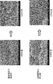
- FIG. 1 is a scanning electron microscope observation image showing the surface of a copper foil for a transparent resin substrate provided with fine concavo-convex structure layers on both sides of an electrolytic copper foil as an example of the copper foil for a transparent resin substrate according to the present invention.
- the surface of the fine concavo-convex structure layer on the electrode surface side and the deposition surface side is shown.
- FIG. 1 shows a planar emission using a field emission type scanning electron microscope at magnifications of 10,000 and 50000 times (inclination angle of 45 ° of the sample at the time of observation with a scanning electron microscope).
- An example of the surface of the fine uneven structure layer is shown.
- FIG. 1 is a scanning electron microscope observation image showing the surface of a copper foil for a transparent resin substrate provided with fine concavo-convex structure layers on both sides of an electrolytic copper foil as an example of the copper foil for a transparent resin substrate according to the present invention.
- FIG. 1 shows a planar emission using a field emission type scanning electron microscope at mag
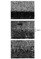
- FIGS. 1 and 2 are scanning electron microscope observation images which shows the cross section of the copper foil for transparent resin base materials shown in FIG.
- FIGS. 1 and 2 countless fine needle-like or plate-like convex portions made of a copper composite compound are observed on the surface of the transparent resin substrate copper foil. It can be confirmed that an extremely fine concavo-convex structure is formed on the surface by densely adhering to each other.
- the convex portion refers to a protruding portion extending in a needle shape or a plate shape from the surface of the copper foil along the surface shape of the copper foil as shown in FIG. 1, and the protruding portion is a copper composite. It is composed of a single crystal of a compound or an aggregate of a plurality of crystals.
- the maximum length of the convex portion is the length of the needle-like or plate-like convex portion when the cross section of the fine concavo-convex structure layer is observed with a field emission type scanning electron microscope. The maximum value is shown. Specifically, as shown in FIG.
- a convex portion extending in a needle shape or a plate shape from the surface of the copper foil in the cross section. Is observed.
- the maximum value of the length from the base end portion to the tip end portion of the convex portion is referred to. In this invention, it is preferable that the maximum length of the said convex-shaped part is 400 nm or less, and it is more preferable that it is 300 nm or less.
- the convex portion becomes shorter, even when another object comes into contact with the surface of the fine concavo-convex structure with a greater force, the convex portion is less likely to be damaged, and the surface shape of the fine concavo-convex structure Is easier to maintain.
- the shorter the maximum length the finer the rugged structure becomes, and due to the surface shape, the function of the fine rugged structure layer as an adhesion layer and the function as an antireflection layer are improved. be able to.
- the length of the tip portion that can be separated and observed from other convex portions is preferably 250 nm or less.
- “the length of the tip portion that can be observed separately from other convex portions refers to the length shown below. .
- the interface between the end portion, that is, the convex portion made of the copper composite compound and the copper foil cannot be observed. Therefore, when the surface of the fine concavo-convex structure layer is observed in a planar manner as described above, it is separated from the other bulges among the bulges adjacent to each other while being densely packed, and is independent as one bulge.
- the portion that can be observed to be present on the surface is called the “tip portion that can be observed separately from other convex portions”, and the length of the tip portion is the tip of the convex portion (that is, the tip portion of the tip portion). The length from the tip) to the position on the most proximal side that can be separated and observed from other convex portions.
- the maximum length of the convex portion is approximately 500 nm or less, and the function as the adhesion layer of the fine concavo-convex structure layer described above, as the antireflection layer Function can be obtained.
- the length of the tip portion of the convex portion is 1 ⁇ 2 or less with respect to the maximum length of the convex portion.
- the ratio is 1 ⁇ 2 or less, the nano-anchor effect due to the fine concavo-convex structure can be exhibited while being separated from other convex portions, and adjacent convex shapes at the base end portion of the convex portions. Since the parts are in close contact with each other while being in contact with each other, the copper foil surface can be densely covered with this fine concavo-convex structure.
- the average thickness of the fine concavo-convex structure layer is preferably 400 nm or less, and more preferably 350 nm or less.
- the average thickness of the fine uneven structure layer shown in FIG. 2 is 250 nm.
- the length and the protruding direction of each convex part forming the fine concavo-convex structure are not constant, and the protruding direction of each convex part is not parallel to the thickness direction of the copper foil. For this reason, the maximum length of the convex portion does not match the maximum thickness of the fine uneven structure layer, and has the relationship of “maximum thickness of the fine uneven structure layer ⁇ maximum length of the convex portion”. .
- the maximum length of the convex portion is approximately 500 nm or less.
- the average thickness of the fine concavo-convex structure layer is in the range of 100 nm to 400 nm, when the transparent resin substrate copper foil is laminated to the transparent resin substrate, the transparent resin substrate copper foil and the transparent resin substrate Good adhesion can be obtained.
- the pitch between the convex portions In the fine concavo-convex structure layer, it is impossible to strictly measure the pitch between the convex portions. However, in consideration of the fact that the maximum length of the convex portions is 500 nm or less and the adjacent convex portions at the base end portion of the convex portions are densely in contact with each other, these convex shapes The parts are considered to be adjacent to each other at a pitch shorter than the wavelength range of visible light (780 nm to 380 nm). Since the needle-like or plate-like convex portions having a maximum length of 500 nm or less are arranged at a pitch shorter than the wavelength range of visible light, visible light incident on the fine concavo-convex structure layer is within the fine concavo-convex structure.
- the fine concavo-convex structure layer contains cuprous oxide exhibiting red or reddish brown, but the surface exhibits dark brown to black having a low brightness equal to or higher than that of a black oxide film mainly composed of cupric oxide. .
- the component ratio of cuprous oxide and cupric oxide will be described later.
- the L * value (lightness) in the CIE-L * a * b * color system on the surface of the fine concavo-convex structure layer is 30 or less, more preferably 25 or less, and even more preferably 20 or less.
- the maximum length of the convex portion forming the fine concavo-convex structure layer may be longer than 500 nm.
- This L * value can be measured using a spectroscopic color difference meter SE2000 manufactured by Nippon Denshoku Industries Co., Ltd., and a white plate attached to the measuring device can be used for lightness calibration, in accordance with JIS Z8722: 2000. . And the measurement of 3 times is performed regarding the same site
- the constituent elements of the fine concavo-convex structure layer are analyzed by X-ray photoelectron spectroscopy (hereinafter referred to as “XPS”).
- XPS X-ray photoelectron spectroscopy
- the ratio of the peak area of Cu (I) to the total area of the peak area of Cu (I) and the peak area of Cu (II) obtained in (1) is 50% or more. It is preferable.
- each peak of Cu (I) and Cu (II) can be separated and detected.
- the Cu (0) peak may be observed overlapping the shoulder portion of the large Cu (I) peak.
- the peak of Cu (0) is observed overlappingly, it shall be considered as a Cu (I) peak including this shoulder part.
- the constituent elements of the copper composite compound forming the fine concavo-convex structure layer are analyzed using XPS, and Cu (I) and 934 appearing at 932.4 eV corresponding to the binding energy of Cu 2p 3/2.
- Each peak obtained by detecting photoelectrons of Cu (II) appearing at .3 eV is separated into waveforms, and the occupied area ratio of the Cu (I) peak is specified from the peak area of each component.
- Quantum 2000 (beam condition: 40 W, 200 um diameter) manufactured by ULVAC-PHI Co., Ltd. is used as an XPS analyzer
- “MultiPack ver. 6.1A” is used as analysis software to perform state / semi-quantitative narrow measurement. be able to.
- the Cu (I) peak is derived from monovalent copper constituting cupric oxide (Cu 2 O). And it is thought that a Cu (II) peak originates in the bivalent copper which comprises cuprous oxide (CuO). Furthermore, it is considered that the Cu (0) peak is derived from zero-valent copper constituting metallic copper. Therefore, when the occupied area ratio of the Cu (I) peak is less than 50%, the proportion of cuprous oxide in the copper composite compound constituting the fine concavo-convex structure layer is smaller than the proportion of cupric oxide. it is conceivable that.
- cuprous oxide compared with cupric oxide, cuprous oxide has high solubility with respect to acids, such as etching liquid.
- the occupied area ratio of the Cu (I) peak is less than 50%, the fine concavo-convex structure layer side of the copper foil for the transparent resin substrate is bonded to the transparent resin substrate, and the copper wiring is formed by the etching method. In this case, the fine concavo-convex structure layer is easily dissolved in the etching solution, and the adhesion between the copper wiring and the transparent resin substrate may be lowered. From this viewpoint, it is preferable that the occupied area ratio of the Cu (I) peak is 70% or more when analyzing the constituent elements of the copper composite compound that forms the fine concavo-convex structure layer by XPS, and it is 80% or more. More preferably, it is particularly preferably 90% or more.
- the occupied area ratio of the Cu (I) peak increases, the component ratio of cupric oxide having higher acid solubility with respect to an etching solution or the like becomes higher than that of cuprous oxide. Accordingly, the acid solubility of the fine concavo-convex structure layer with respect to the etching solution is improved, and it becomes possible to reduce the insertion of the etching solution when forming the copper wiring, and the copper wiring having good adhesion to the transparent resin base material can be obtained. Can be formed.
- the upper limit value of the occupied area ratio of the Cu (I) peak is not particularly limited, but is 99% or less.
- the exclusive area ratio of the Cu (I) peak is preferably 98% or less, and more preferably 95% or less. Note that the occupied area ratio of the Cu (I) peak is calculated by a calculation formula of Cu (I) / ⁇ Cu (I) + Cu (II) ⁇ ⁇ 100 (%).
- the specific surface area (hereinafter simply referred to as “specific surface area”) measured by adsorbing krypton on the surface of the fine concavo-convex structure is preferably 0.035 m 2 / g or more.
- the specific surface area measured in this manner is 0.035 m 2 / g or more
- the average thickness of the fine concavo-convex structure layer is 200 nm or more
- copper is applied to the transparent resin substrate via the fine concavo-convex structure layer. Good adhesion can be secured when the foil (copper foil for transparent resin substrate) is laminated.
- the upper limit value of the specific surface area is not particularly limited, but the fine concavo-convex structure is formed by densely forming needle-like or plate-like convex portions having a maximum length of 500 nm or less. In order to satisfy the shape, the upper limit value of the specific surface area is about 0.3 m 2 / g in calculation, and actually about 0.2 m 2 / g is the upper limit value.
- the specific surface area is measured by using a specific surface area / pore distribution measuring device 3Flex manufactured by Micromeritics Co., Ltd. as a pretreatment by heating the sample at 300 ° C. for 2 hours. The above measurement can be performed by using krypton (Kr).
- the copper foil for transparent resin base materials mentioned above can be manufactured as follows, for example. First, an oxidation treatment is performed on the surface of the copper foil, and a fine concavo-convex structure is formed on the copper foil surface by needle-like or plate-like convex portions made of a copper composite compound containing cupric oxide as a main component.
- the oxidation treatment can be performed, for example, by a wet method in which a treatment solution described later and a copper foil are brought into contact with each other.
- a fine concavo-convex structure layer having a fine concavo-convex structure formed by needle-like or plate-like convex portions having a maximum length of 500 nm or less made of a copper composite compound can be formed.
- an alkaline solution (hereinafter referred to as an alkaline solution) that oxidizes the copper surface and hardly erodes cuprous oxide can be used.
- an alkaline solution that oxidizes the copper surface and hardly erodes cuprous oxide
- cupric oxide needle-like crystals generated on the surface grow longer than 500 nm, making it difficult to form the fine concavo-convex structure layer. That is, in order to form the fine concavo-convex structure layer referred to in the present invention, it is necessary to control so that the acicular crystals of cupric oxide do not grow too much. Therefore, it is preferable to use an alkaline solution containing an oxidation inhibitor capable of suppressing oxidation on the copper foil surface as the treatment solution.
- the oxidation inhibitor examples include amino silane coupling agents. If the copper foil surface is oxidized using an alkali solution containing an amino silane coupling agent, the amino silane coupling agent in the alkali solution is adsorbed on the surface of the copper foil, and the copper foil surface by the alkali solution Can be suppressed. As a result, the growth of cupric oxide needle-like crystals can be suppressed, and the fine concavo-convex structure layer having an extremely fine concavo-convex structure on the order of nm can be formed.
- amino-based silane coupling agent examples include N-2- (aminoethyl) -3-aminopropylmethyldimethoxysilane, N-2- (aminoethyl) -3-aminopropyltrimethoxysilane, 3- Aminopropyltrimethoxysilane, 3-aminopropyltriethoxysilane, 3-triethoxysilyl-N- (1,3-dimethyl-butylidene) propylamine, N-phenyl-3-aminopropyltrimethoxysilane, etc. may be used. It can. All of these are dissolved in an alkaline solution, stably held in the alkaline solution, and exhibit the effect of suppressing oxidation of the copper foil surface described above.
- the fine concavo-convex structure formed by subjecting the surface of the copper foil to an oxidation treatment with an alkaline solution containing an amino-based silane coupling agent is substantially maintained even after the reduction treatment.
- the As a result, it has a fine concavo-convex structure on the order of nm formed by needle-like or plate-like convex portions having a maximum length of 500 nm or less, including cuprous oxide and cupric oxide, and having a maximum length of 500 nm or less.
- An uneven structure layer can be obtained.
- the Cu (I) obtained when analyzing the constituent elements of the copper composite compound forming the fine concavo-convex structure layer described above.
- the occupied area ratio of the peak of Cu (I) can be appropriately adjusted with respect to the total area of the peak area and the peak area of Cu (II).
- the fine concavo-convex structure layer contains cuprous oxide and cupric oxide, and has a high probability of containing a trace amount of copper carbonate in addition to a trace amount of metal copper.
- the fine uneven structure layer is formed on both surfaces of the copper foil by a method such as immersing the copper foil in the treatment solution. It can be formed easily.
- a transparent resin substrate with fine wiring according to the present invention In the transparent resin base material with fine wiring according to the present invention, a copper wiring having a line width of 10 ⁇ m or less is provided on the surface of the transparent resin base material.
- the copper wiring includes a copper foil layer, cuprous oxide, A fine concavo-convex structure layer having a fine concavo-convex structure formed by needle-like or plate-like convex portions having a maximum length of 500 nm or less, including cupric oxide and comprising these copper composite compounds, To do.
- the transparent resin substrate with fine wiring can be suitably used as a material for manufacturing a fine wiring type transparent electrode such as a capacitive touch panel.
- various modes can be considered for the transparent resin substrate with fine wiring, here, the first mode shown in FIG. 3 (B) and the second mode shown in FIG. 5 (B) will be mainly described. To do.
- the transparent resin base material 10 with a fine wiring of a 1st aspect is demonstrated, referring FIG.3 and FIG.4.
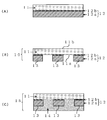
- the transparent resin base material 10 with fine wiring according to the first aspect is obtained by laminating the copper foil 12 for a transparent resin base material provided with the fine uneven structure layer 12b on one side of the copper foil 12a on one side of the transparent resin base material 11. (See FIG. 3 (A)), which is obtained by forming a wiring pattern by an etching method.
- the line width is 10 ⁇ m or less on one side 11a of the transparent resin substrate 11.
- a plurality of copper wirings 13 are provided. In the example shown in FIG.
- the copper wiring 13 is in close contact with the transparent resin base material 11 via the fine concavo-convex structure layer 12b provided on one surface of the copper foil layer 12a.
- These transparent resin base material 11 and fine concavo-convex structure layer 12b have the same configuration as the transparent resin base material and fine concavo-convex structure layer described in the above-described copper foil for transparent resin base material, and copper foil layer 12a It has the same configuration as the copper foil described above. Accordingly, in the first aspect, the description of the same contents as those described above will be omitted, but it should be understood that they have the same functions and effects as described above as long as they have the same configuration as above. .
- the fine concavo-convex structure layer 12b included in the copper wiring 13 functions as an adhesion layer for bringing the transparent resin substrate 11 and the copper foil layer 12a into close contact with each other.
- the needle-like or plate-like convex portions are transparent resin in the process in which the resin material constituting the transparent resin base material 11 is melted and cured by heat.
- the transparent resin base material 11 and the copper foil layer 12a have good adhesiveness due to the fine uneven structure layer 12b.
- the visible light transmitted through the transparent resin base material 11 is a fine uneven structure of the copper wiring 13 provided on the one surface 11 a side of the transparent resin base material 11.
- the light enters the layer 12b.
- the fine concavo-convex structure layer 12b also functions as an antireflection layer as described above, the reflection of the incident light is suppressed.
- a transparent optical adhesive film layer (hereinafter referred to as OCA layer) 14 is provided on one side 11 a of the transparent resin substrate 11 so as to cover the exposed portion of the one side 11 a and the copper wiring 13, thereby forming a set of electrode materials 15. (See FIG. 3C). As shown in FIG.
- the fine uneven structure layer 12b is provided on the copper wiring 13 on the side viewed from the user, reflection of light incident on the copper wiring 13 can be prevented, and the display It is possible to prevent a decrease in image quality by preventing a decrease in contrast of the displayed image. Furthermore, since the fine concavo-convex structure layer 12b is provided on the viewing side from the user, it is not necessary to apply blackening treatment again after the wiring pattern is formed. For this reason, an extremely fine copper wiring having a line width of 10 ⁇ m or less, preferably a line width of 6 ⁇ m or less can be formed well.
- the touch panel shown in FIG. 4E is manufactured using the transparent resin base material 10 with fine wiring, the transparent resin base material 11 and the copper wiring 13 are satisfactorily adhered to each other by the fine concavo-convex structure layer 12b. Can do.
- the transparent resin base material 11 bends and a stress is applied between the transparent resin base material 11 and the copper wiring 13.
- stress is repeatedly applied between the transparent resin base material 11 and the copper wiring 13.
- the transparent resin base material 11 and the copper wiring 13 are in close contact with each other through the fine concavo-convex structure layer 12b, even if stress is repeatedly applied between the two, the copper wiring 13 can be prevented from peeling from the transparent resin substrate 11.
- the fine uneven structure layer 12b is provided only on one surface of the copper foil layer 12a. You may provide the fine uneven structure layer 12b on both surfaces.
- the transparent resin base material copper foil provided with the fine concavo-convex structure layer 12b on both surfaces of the copper foil 12a is bonded to the transparent resin base material 11, and the same as in FIG. If a wiring pattern is formed by an etching method in the same manner as in FIG. 3B after obtaining the laminate, the copper wiring 13 having the fine concavo-convex structure layers 12b on both sides of the copper foil layer 12a can be obtained.
- the fine concavo-convex structure layer 12b is provided on both surfaces of the copper foil layer 12a, the fine concavo-convex structure layer 12b is provided not only between the copper wiring 13 and the transparent resin substrate 11, but also between the copper wiring 13 and the OCA layer 14. It can be made to adhere well through. Therefore, even when the touch panel is repeatedly operated, the adhesion between the copper wiring 13 and the transparent resin substrate 11 can be maintained, and the adhesion between the copper wiring 13 and the OCA layer 14 can be maintained.
- the thickness of the copper foil layer 12a is preferably smaller from the viewpoint of suppressing the specular reflection of incident light on the side surface of the copper foil layer 12a, and more preferably 12 ⁇ m or less. preferable.
- the thickness of the copper foil layer 12a is the same as the thickness of the copper foil described above, and the thinner the copper foil layer 12a is also preferable in forming the copper wiring 13 with a favorable etching factor.
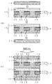
- the transparent resin base material 20 with fine wiring according to the second embodiment is a transparent resin provided with fine concavo-convex structure layers 22b on both sides of a copper foil 22a on both sides of the transparent resin base material 21.
- the transparent resin base material 21 A plurality of copper wirings 22 each having a line width of 10 ⁇ m or less are provided on both surfaces.
- the transparent resin base material 21, the copper wiring 23, the copper foil layer 22a, the fine uneven structure layer 22b, and the transparent resin base material copper foil 22 are respectively the copper foil for the transparent resin base material or the first aspect described above. Since the transparent resin base material 11, the copper wiring 13, the copper foil layer 12a, the fine concavo-convex structure layer 12b, and the transparent resin base material copper foil 12 described in the transparent resin base material 10 with fine wiring have the same configuration, Description of duplicate contents is omitted. However, as long as they have the same configuration as described above, they naturally exhibit the same functions and effects.
- the transparent resin base material 20 with a fine wiring of the second aspect since the copper wiring 23 is provided on both surfaces of the transparent resin base material 21, it can be a fine wiring type transparent electrode in this state.
- an OCA layer 24 is provided on each of the two surfaces in the same manner as in the first embodiment (see FIG. 5C), and in the laminated body 25 provided with the OCA layer 24, the side to be viewed from the user side.
- a cover glass 26 on the surface of the OCA layer 24 and further laminating another transparent resin base material 27 on the surface of the OCA layer 24 on the other surface side, a capacitive touch panel can be obtained.
- the fine wiring type transparent electrode when the fine wiring type transparent electrode is formed by providing the copper wiring 23 on both surfaces of the transparent resin substrate 21, unlike the fine wiring type transparent electrode of the first aspect, the transparent resin base The layer of the material 21 can be further reduced. For this reason, the transmittance
- the copper wiring 23 provided with the fine concavo-convex structure layer 22b2 on both surfaces is provided on both surfaces of the transparent resin substrate 21.
- the said fine wiring type resin base material 20 is used, reflection of the light which injects into the copper wiring 23 can be prevented even if any surface is made into the visual recognition side from a user.
- the copper wiring 23 provided on the surface of the transparent resin base 21 opposite to the viewing side from the user is connected to the transparent resin base 21.
- the copper wiring 23 provided with the fine uneven structure layer 22b only on the bonding surface is sufficient.
- the copper wiring 23 provided on the surface opposite to the side viewed from the user is provided only with the transparent resin base material 21 by providing the fine uneven structure layer 22b on both surfaces. Instead, the copper wiring having good adhesion to the OCA layer 24 can be obtained.
- the copper foil for transparent resin base materials concerning this invention is not limited to the following Examples, The meaning of this invention is shown. Of course, it can be changed as appropriate without departing from the scope.
- a copper electrolyte solution having the composition described below is used, DSA is used as the anode, and a cathode (a titanium plate electrode whose surface is polished with No. 2000 polishing paper), the liquid temperature is 50 ° C., and the current density is 60 A / dm 2.
- the electrolytic copper foil having a thickness of 18 ⁇ m was obtained. And the fine uneven structure layer was formed in both surfaces of the electrolytic copper foil in the following procedures, and it was set as the copper foil for transparent resin base materials which concerns on this invention.
- Copper electrolyte composition Copper concentration: 80 g / L Free sulfuric acid concentration: 140 g / L Bis (3-sulfopropyl) disulfide concentration: 5 mg / L Diallyldimethylammonium chloride polymer concentration: 30 mg / L Chlorine concentration: 25mg / L
- the electrolytic copper foil was immersed in an aqueous sodium hydroxide solution, subjected to alkali degreasing treatment, and washed with water. Then, the electrolytic copper foil after the alkaline degreasing treatment was immersed in a sulfuric acid solution having a hydrogen peroxide concentration of 1 mass% and a sulfuric acid concentration of 5 mass% for 5 minutes, and then washed with water.
- a predetermined oxidation treatment time (1 minute, 2 minutes, 4 minutes, 10 minutes) is immersed in a sodium hydroxide solution containing 10 g / L, and both surfaces of the electrolytic copper foil are subjected to oxidation treatment. Four types of samples were obtained.
- Table 1 shows the length of the tip portion of the convex portion forming the fine concavo-convex structure together with the maximum length of the convex portion.
- tip part are as having mentioned above.
- the same electrolytic copper foil as in the example was used, and after the preliminary treatment was performed in the same manner as in the example, the blackening treatment was performed on both surfaces of the electrolytic copper foil under the following conditions. It was set as the copper foil for materials.
- Blackening treatment The above preliminary solution in an aqueous solution having a temperature of 85 ° C. containing 10 vol% of “PRO BOND 80A OXIDE SOLUTION” and 20 vol% of “PRO BOND 80A OXIDE SOLUTION”, which is an oxidation treatment solution manufactured by Rohm and Haas Electronic Materials Co., Ltd.
- the electrolytic copper foil that had been treated was immersed for 5 minutes and subjected to blackening treatment.
- Table 1 shows the maximum length of the convex portion (needle crystal) and the length of the tip portion formed on the surface of the copper foil by the blackening treatment.
- the state of the surface of the blackening treatment layer of the copper foil for a transparent resin substrate obtained in the comparative example was analyzed using XPS.
- the presence of “Cu (I)” and “Cu (II)” was confirmed, but the presence of “—COO group” was not confirmed.
- Table 1 shows the occupied area ratio, specific surface area, and lightness (L * value) of the Cu (I) peak of the copper foil for transparent resin base material obtained in this comparative example.
- the copper foil for transparent resin base materials contains cuprous oxide and cupric oxide on the surface of copper foil, and the maximum length which consists of these copper complex compounds is a needle shape or plate shape with a maximum of 500 nm or less.
- the copper foil for a transparent resin base material is less likely to be powdered off during handling, etc., can maintain a fine uneven structure on the surface, and fine powder of copper oxide is scattered or adhered to the surroundings. Can be prevented. Therefore, when a fine wiring type transparent electrode such as a touch panel is manufactured using the copper foil for a transparent resin base material, it may be difficult to cause unevenness in the antireflection effect due to powder falling and poor insulation between wirings. it can. For this reason, it becomes easy to provide the said fine uneven structure layer on both surfaces of copper foil.
- the said fine concavo-convex structure layer contains cuprous oxide and cupric oxide, compared with the conventional black copper oxide film, according to the ratio containing cuprous oxide, etching liquid It is possible to improve the acid solubility resistance against the like. Therefore, when the fine concavo-convex structure layer side is bonded to the transparent resin base material side and the copper wiring is formed by the etching method, the fine concavo-convex structure layer dissolves and the adhesion between the transparent resin base material and the copper wiring decreases. Can be suppressed.
- the fine concavo-convex structure consists of needle-like or plate-like convex portions having a maximum length of 500 nm or less, the maximum pitch between the convex portions tends to be shorter than the wavelength range of visible light.
- the maximum pitch is less than or equal to the wavelength range of visible light, the surface reflectance of visible light incident on the fine concavo-convex structure layer can be extremely reduced, and a layer having a high antireflection function can be obtained.
- the fine concavo-convex structure layer when the fine concavo-convex structure layer is provided on both surfaces of the copper foil, a double-sided black copper foil having both sides dark brown to black can be obtained. If this is utilized, the fine concavo-convex structure layer provided on one side of the copper foil ensures adhesion to the transparent resin substrate, and the fine concavo-convex structure layer provided on the other side of the copper foil provides copper. Specular reflection of visible light incident on the other surface side of the foil can be suppressed.
- the adhesiveness with the transparent resin substrate is good, and the transparent resin substrate side and its side A copper wiring having a layer having a high antireflection function can be formed on either side.
Landscapes
- Chemical & Material Sciences (AREA)
- Chemical Kinetics & Catalysis (AREA)
- Engineering & Computer Science (AREA)
- Materials Engineering (AREA)
- Mechanical Engineering (AREA)
- Metallurgy (AREA)
- Organic Chemistry (AREA)
- Laminated Bodies (AREA)
- Parts Printed On Printed Circuit Boards (AREA)
- Other Surface Treatments For Metallic Materials (AREA)
- Non-Insulated Conductors (AREA)
Abstract
本願発明の課題は、透明樹脂基材の表面に耐擦傷性及び耐酸溶解性が高く、反射防止効果の高い極微細な銅配線を形成する際に好適な透明樹脂基材用銅箔、微細配線付透明樹脂基材及び微細配線付透明樹脂基材の製造方法を提供することにある。 上記課題を解決するために、透明樹脂基材の表面に銅配線を形成するための透明樹脂基材用銅箔として、銅箔の表面に、酸化第一銅及び酸化第二銅を含み、これら銅複合化合物からなる最大長さが500nm以下の針状又は板状の凸状部により形成された微細凹凸構造を有する微細凹凸構造層を備えたことを特徴とする透明樹脂基材用銅箔を用いる。
Description
本願発明は、透明樹脂基材用銅箔及び微細銅配線付透明樹脂基材に関し、特にタッチパネル等の微細配線型透明電極の製造材料に好適な透明樹脂基材用銅箔及び微細銅配線付透明樹脂基材に関する。
従来より、スマートフォン等の携帯電話、携帯ゲーム機などの携帯用電子機器の入力装置としてタッチパネルが広く採用されている。また、近年では、タブレット端末やパーソナルコンピュータなどの比較的ディスプレイサイズの大きな電子機器の入力装置としても、タッチパネルが採用されるようになってきており、タッチパネルの大面積化が進行している。スマートフォン等の静電容量式のタッチパネルでは、表面の静電容量の変化を検知するため、主にITO(酸化インジウムスズ)電極材料を利用した透明電極が用いられてきたが、近年、タッチパネルの大面積化に伴い、透明樹脂フィルムの表面に銅等の金属からなる微細配線パターンを設けた微細配線型透明電極を用いることが提案されている。ITO電極と比較すると微細配線型透明電極は表面抵抗が小さく、タッチパネルの大面積化を図ることが容易になるためである。
このような微細配線型透明電極として、特許文献1には、ポリエチレンテレフタレート(以下、「PET」と略する。)フィルムの片面にX方向に延びる等間隔のストライプ状銅配線を設け、当該PETフィルムの他面には、当該X方向と交差するY方向に延びる等間隔のストライプ状銅配線を設けた微細配線型透明電極(メッシュ電極)が開示されている。従来、この種の微細配線型電極では、PETフィルムの片面に所定の方向に延びるストライプ状銅配線を備えた電極材を二組用意し、各ストライプ状銅配線が交差するように電極材を積層させた微細配線型透明電極が提案されてきた。この従来の微細配線型透明電極と比較すると、特許文献1に記載の微細配線型透明電極は、PETフィルムの両面にストライプ状銅配線を設けることにより、PETフィルムの層を二層から一層に削減することができる。このため、微細配線型透明電極の可視光の透過率を従来よりも高くすることができ、さらに工数及びコストを削減することができる。
また、特許文献1に記載の微細配線型透明電極では、ストライプ状銅配線において、ディスプレイ上に当該微細配線型透明電極を搭載したときにユーザーから視認される側となる面に、それぞれ黒色酸化銅被膜が設けられている。これにより、ユーザー側からストライプ状銅配線に入射した光が鏡面反射するのを防止し、コントラストを向上させ、画質の低下を抑制するものとしている。この黒色酸化銅被膜を銅配線に設ける方法として、特許文献1には、銅箔又は銅配線の表面に黒化処理を施す方法が記載されている。
ところで、配線パターン形成後に黒化処理を施した場合、銅配線の表面がエッチングされる。このため銅配線の表面が黒色化されるまでの間に、銅配線の線幅や厚みが減少する。近年、タッチパネルの大面積化等に伴い、微細配線型透明電極においては、例えば、10μm以下、好ましくは6μm以下の極微細な銅配線を形成することが求められている。このような極微細な銅配線を形成する場合、配線パターン形成後に黒化処理を施したのでは、銅配線の表面が黒色化されるまでの間に銅配線がエッチングにより除去されてしまう恐れがある。従って、当該方法では、極微細な銅配線を実現することは困難である。
一方、予め黒化処理が施された銅箔を用い、この黒色酸化銅皮膜側の面をユーザーから視認される側に配置してパターン形成を行えば、配線パターン形成後に黒化処理を施す必要がない。しかしながら、この場合、次の問題が生じる。銅箔に対して黒化処理を施した場合、銅箔の表面には酸化銅の針状結晶が形成される。黒化処理で生成される針状結晶は、一般に、長く脆いため、銅箔の表面に他の物体が接触すると、針状結晶が折れて、酸化銅の微粉が周囲に飛散又は付着する粉落ちと称される現象が生じやすい。この粉落ちが生じた場合、銅箔の表面の凹凸構造が崩れるため、当該黒色酸化銅被膜表面の光の反射防止効果にムラが生じる恐れがある。また、銅配線間に酸化銅の微粉が付着した場合には、絶縁不良等の問題が生じる恐れがある。
さらに、特許文献1には、上記黒色酸化銅被膜の表面が黒色であることが記載されている。従って、特許文献1に記載の黒色酸化銅被膜の主成分は酸化第二銅(CuO)であると考えられる。しかしながら、酸化第二銅は、酸化第一銅(Cu2O)と比較するとエッチング液等の酸に対する溶解性が高い。このため、当該黒色酸化銅被膜側をPETフィルムに張り合わせて配線パターンを形成した場合、エッチング液に黒色酸化銅被膜が溶解して、銅配線と透明樹脂基材との界面が一部剥離し、両者の密着性が低下する恐れがある。これを回避するために、例えば、黒化処理の後に還元処理を施して、酸化第二銅の一部を酸化第一銅に還元することが考えられる。しかしながら、この場合、酸化第一銅の成分比率に応じて当該黒色酸化銅被膜の表面の明度が高くなり、茶色味又は赤味を帯びてくることから、十分な反射防止効果を得ることができない恐れがある。
本願発明の課題は、透明樹脂基材の表面に、耐擦傷性及び耐酸溶解性が高く反射防止効果の高い極微細な銅配線を形成する際に好適な透明樹脂基材用銅箔、微細配線付透明樹脂基材及び微細配線付透明樹脂基材の製造方法を提供することにある。
そこで、本願発明者等の鋭意研究の結果、以下に示す微細凹凸構造層を銅箔の表面に設けることにより、上記課題を解決するに至った。
本願発明に係る透明樹脂基材用銅箔は、透明樹脂基材の表面に銅配線を形成するための透明樹脂基材用銅箔であって、銅箔の表面に、酸化第一銅及び酸化第二銅を含み、これら銅複合化合物からなる最大長さが500nm以下の針状又は板状の凸状部により形成された微細凹凸構造を有する微細凹凸構造層を備えたことを特徴とする。
本願発明に係る微細銅配線付透明樹脂基材は、透明樹脂基材の表面に、線幅が10μm以下の銅配線が設けられた微細銅配線付透明樹脂基材であって、当該銅配線は、銅箔層と、酸化第一銅及び酸化第二銅を含み、これら銅複合化合物からなる最大長さが500nm以下の針状又は板状の凸状部により形成された微細凹凸構造を有する微細凹凸構造層とを備えたことを特徴とする。
本願発明によれば、透明樹脂基材用銅箔は、銅箔の表面に酸化第一銅及び酸化第二銅を含み、これら銅複合化合物からなる最大長さが500nm以下の針状又は板状の凸状部により形成された微細凹凸構造を有する微細凹凸構造層を備えている。すなわち、当該微細凹凸構造は、最大長さが500nm以下の針状又は板状の凸状部により形成されていることから、銅箔の表面から500nmを超えて長く突出する針状又は板状の凸状部が存在しない。このため、当該微細凹凸構造層の表面に他の物体が接触したとしても、これらの針状又は板状の凸状部は短いため折れにくく、耐擦傷性が高い。従って、当該透明樹脂基材用銅箔は、ハンドリングの際等にいわゆる粉落ちが生じにくく、表面の微細凹凸構造を維持することができ、周囲に酸化銅の微粉が飛散したり、付着するのを防止することができる。従って、当該透明樹脂基材用銅箔を用いて、タッチパネル等の微細配線型透明電極を製造した場合、粉落ちに起因した反射防止効果のムラや、配線間の絶縁不良を生じにくくすることができる。このため、銅箔の両面に当該微細凹凸構造層を設けることも容易になる。
また、本願発明において、当該微細凹凸構造層は、酸化第一銅及び酸化第二銅を含むため、従来の黒色酸化銅被膜と比較すると、酸化第一銅を含有する比率に応じて、エッチング液等に対する耐酸溶解性を向上させることができる。従って、微細凹凸構造層側を透明樹脂基材側に張り合わせて、エッチング法により銅配線を形成する際に微細凹凸構造層が溶解して、透明樹脂基材と銅配線との密着性が低下するのを抑制することができる。
さらに、当該微細凹凸構造は最大長さが500nm以下の針状又は板状の凸状部からなるため、凸状部間の最大ピッチは可視光の波長域よりも短くなる傾向にある。最大ピッチが可視光の波長域以下である場合、当該微細凹凸構造層に入射した可視光の表面反射率を極めて小さくすることができ、高い反射防止機能を有する層とすることができる。
本願発明に係る透明樹脂基材用銅箔において、銅箔の両面に当該微細凹凸構造層を設けた場合、両面が暗褐色~黒色の両面黒色銅箔とすることができる。これを利用すれば、銅箔の片面側に設けられた微細凹凸構造層により、透明樹脂基材との密着性を担保すると共に、銅箔の他面側に設けられた微細凹凸構造層により銅箔の他面側に入射した可視光の鏡面反射を抑制することができる。つまり、両面に微細凹凸構造層を備えた銅箔を用いて、上記微細配線型透明電極を製造すれば、透明樹脂基材との密着性が良好であり、且つ、透明樹脂基材側及びその反対側のいずれにも高い反射防止機能を有する層を備えた銅配線を形成することができる。
以下、本願発明に係る透明樹脂基材用銅箔及び微細銅配線付透明樹脂基材について説明する。
1.透明樹脂基材用銅箔
まず、本願発明に係る透明樹脂基材用銅箔について説明する。本願発明に係る透明樹脂基材用銅箔は、透明樹脂基材の表面に銅配線を形成するための透明樹脂基材用銅箔であって、銅箔の表面に、酸化第一銅及び酸化第二銅を含み、これら銅複合化合物からなる最大長さが500nm以下の針状又は板状の凸状部により形成された微細凹凸構造を有する微細凹凸構造層を備えたことを特徴とする。
まず、本願発明に係る透明樹脂基材用銅箔について説明する。本願発明に係る透明樹脂基材用銅箔は、透明樹脂基材の表面に銅配線を形成するための透明樹脂基材用銅箔であって、銅箔の表面に、酸化第一銅及び酸化第二銅を含み、これら銅複合化合物からなる最大長さが500nm以下の針状又は板状の凸状部により形成された微細凹凸構造を有する微細凹凸構造層を備えたことを特徴とする。
当該透明樹脂基材用銅箔は、例えば、静電容量式のタッチパネルの微細配線型透明電極等を製造する際に用いることができる。透明樹脂基材に対して、微細凹凸構造側を張り合わせれば、ナノアンカー効果により、透明樹脂基材と銅箔とを良好に密着させることができる。すなわち、当該微細凹凸構造層は透明樹脂基材との密着層として機能させることができる。
また、当該微細凹凸構造層の表面は、その極微細な凹凸形状に起因して暗褐色~黒色を呈し、当該微細凹凸構造層に入射した可視光の表面反射率を極めて小さくすることができる。すなわち、当該微細凹凸構造層を光が入射する側に配置すれば、当該微細凹凸構造層を反射防止層として機能させることができる。従って、当該透明樹脂基材用銅箔を用いてタッチパネル等の微細配線型透明電極を製造する際に、タッチパネル等の最終製品態様において、当該微細配線型透明電極に対して光が入射する側に、微細凹凸構造層が配置されるようにして銅配線を形成すれば、銅配線形成後に黒化処理等による銅配線表面に対する反射防止処理を施す必要がなく、工程数を削減することができる。また、銅配線形成後に黒化処理を施した場合、黒化処理の過程で銅配線の表面がエッチングされて、配線幅が狭くなったり、銅配線自体が除去される恐れがある。しかしながら、最終製品態様において、当該微細凹凸構造層側を光が入射する側に配置して、銅配線を形成すれば、反射防止層を備えた10μm以下、好ましくは6μm以下の線幅の極微細な銅配線を透明樹脂基材上に良好に形成することができる。以下、各要素毎に説明する。
(1)透明樹脂基材
まず、透明樹脂基材について説明する。透明樹脂基材は、例えば、可視光の透過率が80%以上の透明な樹脂製の板状基材又はフィルム状基材であり、当該可視光の透過率は85%以上であることが好ましく、90%以上であることが好ましい。当該条件を満たす樹脂基材であれば、透明樹脂基材の材質は特に限定されるものではなく、当該透明樹脂基材用銅箔の用途に応じて、適宜適切なものを用いることができる。例えば、本願発明に係る透明樹脂基材用銅箔を用いて、タッチパネル等の微細配線型透明電極を製造する場合、可視光の透過率が80%以上のポリエチレンテレフタレート樹脂(PET)基材、ポリエチレンナフタレート樹脂(PEN)基材、ポリイミド樹脂(PI)基材等を好適に用いることができる。
まず、透明樹脂基材について説明する。透明樹脂基材は、例えば、可視光の透過率が80%以上の透明な樹脂製の板状基材又はフィルム状基材であり、当該可視光の透過率は85%以上であることが好ましく、90%以上であることが好ましい。当該条件を満たす樹脂基材であれば、透明樹脂基材の材質は特に限定されるものではなく、当該透明樹脂基材用銅箔の用途に応じて、適宜適切なものを用いることができる。例えば、本願発明に係る透明樹脂基材用銅箔を用いて、タッチパネル等の微細配線型透明電極を製造する場合、可視光の透過率が80%以上のポリエチレンテレフタレート樹脂(PET)基材、ポリエチレンナフタレート樹脂(PEN)基材、ポリイミド樹脂(PI)基材等を好適に用いることができる。
(2)銅箔
本願発明において、銅箔についても特に限定されるものではなく、電解銅箔、圧延銅箔のいずれであってもよい。また、本願発明において、銅箔の厚さについても、特に限定されるものではない。しかしながら、当該透明樹脂基材上に、例えば、現在主流である5μm~75μmの銅配線を形成することを考慮すると、当該銅箔の厚みは35μm以下であることが好ましい。但し、銅箔の厚みが薄い方が、極微細な配線パターンを良好なエッチングファクタで形成することが容易になる。従って、より線幅の狭い配線パターンを良好なエッチングファクタで形成するには、銅箔の厚みは18μm以下であることが好ましく、12μm以下であることがより好ましい。厚みのより薄い銅箔を用いることにより、例えば、ボトム幅が3μmの極微細な配線パターンの形成も可能になる。しかしながら、透明樹脂基材の表面に形成された銅配線の厚みが薄くなると、電気抵抗が大きくなるため大型のタッチパネル等に適用できなくなる。従って、電気抵抗を小さくするという観点から、銅箔の厚みは5μm以上であることが好ましく、7μm以上であることがより好ましい。
本願発明において、銅箔についても特に限定されるものではなく、電解銅箔、圧延銅箔のいずれであってもよい。また、本願発明において、銅箔の厚さについても、特に限定されるものではない。しかしながら、当該透明樹脂基材上に、例えば、現在主流である5μm~75μmの銅配線を形成することを考慮すると、当該銅箔の厚みは35μm以下であることが好ましい。但し、銅箔の厚みが薄い方が、極微細な配線パターンを良好なエッチングファクタで形成することが容易になる。従って、より線幅の狭い配線パターンを良好なエッチングファクタで形成するには、銅箔の厚みは18μm以下であることが好ましく、12μm以下であることがより好ましい。厚みのより薄い銅箔を用いることにより、例えば、ボトム幅が3μmの極微細な配線パターンの形成も可能になる。しかしながら、透明樹脂基材の表面に形成された銅配線の厚みが薄くなると、電気抵抗が大きくなるため大型のタッチパネル等に適用できなくなる。従って、電気抵抗を小さくするという観点から、銅箔の厚みは5μm以上であることが好ましく、7μm以上であることがより好ましい。
(3)微細凹凸構造層
次に、微細凹凸構造層について説明する。本願発明において、微細凹凸構造層は上述したとおり、銅箔の表面に設けられた酸化第一銅及び酸化第二銅を含み、これら銅複合化合物からなる最大長さが500nm以下の針状又は板状の凸状部により形成された微細凹凸構造を有する微細凹凸構造層である。
次に、微細凹凸構造層について説明する。本願発明において、微細凹凸構造層は上述したとおり、銅箔の表面に設けられた酸化第一銅及び酸化第二銅を含み、これら銅複合化合物からなる最大長さが500nm以下の針状又は板状の凸状部により形成された微細凹凸構造を有する微細凹凸構造層である。
本願発明では、最大長さが500nm以下の針状又は板状の凸状部により微細凹凸構造を形成することにより、当該微細凹凸構造層の表面に他の物体が接触したとしても、凸状部の長さが短いため、折れる等の損傷が生じにくい。つまり、当該微細凹凸構造層は、従来の黒色酸化銅皮膜と比較すると、表面の凸状部(若しくは針状結晶)の長さが短く、耐擦傷性が高いため、ハンドリングの際等にいわゆる粉落ちが生じず、表面の微細凹凸構造を維持することができ、周囲に酸化銅の微粉が飛散したり付着するのを防止することができる。従って、当該透明樹脂基材用銅箔を用いて、上記微細配線型透明電極等を製造した場合、粉落ちに起因する反射防止効果のムラを防止することができ、配線間の絶縁不良を生じにくくすることができる。
次に、図1及び図2を参照しながら、当該微細凹凸構造についてより詳細に説明する。図1は、本願発明に係る透明樹脂基材用銅箔の一例として、電解銅箔の両面に微細凹凸構造層を備えた透明樹脂基材用銅箔の表面を示した走査型電子顕微鏡観察像であり、電極面側及び析出面側の微細凹凸構造層の表面をそれぞれ示している。より具体的には、図1は、電界放射タイプの走査型電子顕微鏡を用いて、10000倍及び50000倍の倍率で、平面的(走査型電子顕微鏡観察時の試料の傾斜角45°)に観察したときの微細凹凸構造層の表面の一例を示したものである。また、図2は、図1に示す透明樹脂基材用銅箔の断面を示す走査型電子顕微鏡観察像である。図1及び図2に示すように、当該透明樹脂基材用銅箔の表面には、銅複合化合物からなる微細な針状又は板状の凸状部が無数に観察され、これらの凸状部が互いに隣接しながら密集することにより表面に極微細な凹凸構造を形成していることが確認できる。
ここで、上記凸状部とは、図1に示すように銅箔の表面形状に沿って、当該銅箔の表面から針状又は板状に延びた突出部分をいい、当該突出部分は銅複合化合物の単結晶又は複数の結晶の集合体により構成されている。そして、当該凸状部の最大長さとは、当該微細凹凸構造層の断面を電界放射タイプの走査型電子顕微鏡で観察したときに、この針状又は板状の凸状部の長さを測定したときの最大値を示したものである。具体的には、図2に示すように、当該透明樹脂基材の断面を上記走査型電子顕微鏡で観察したときに、その断面において銅箔の表面から針状又は板状に延びた凸状部が観察される。この凸状部の基端部から先端部までの長さの最大値をいう。本願発明において、当該凸状部の最大長さは400nm以下であることが好ましく、300nm以下であることがより好ましい。凸状部の最大長さが短くなる程、当該微細凹凸構造の表面に他の物体がより大きな力で接触した場合にも、凸状部が損傷を受けにくくなり、当該微細凹凸構造の表面形状を維持することが容易になる。また、最大長さが短くなるほど表面がより微細な凹凸構造となり、その表面形状に起因して、当該微細凹凸構造層の密着層としての機能、反射防止層としての機能をより良好なものにすることができる。
また、本願発明に係る透明樹脂基材用銅箔において、走査型顕微鏡を用いて、傾斜角45°、50000倍以上の倍率で当該微細凹凸構造層の表面を平面的に観察したときに、互いに隣接する凸状部のうち、他の凸状部と分離観察可能な先端部分の長さが250nm以下であることが好ましい。ここで、「他の凸状部と分離観察可能な先端部分の長さ(以下、「先端部分の長さ」と略する場合があるものとする)」とは、以下に示す長さをいう。走査型電子顕微鏡により微細凹凸構造層の表面を平面的に観察すると、図1を参照しながら説明したとおり、凸状部が互いに隣接しながら密集して設けられているため、凸状部の基端部、すなわち銅複合化合物からなる凸状部と銅箔との界面を観察することができない。そこで、上述のように微細凹凸構造層の表面を平面的に観察したときに、互いに密集しながら隣接する凸状部のうち、他の凸状部と分離して、一つの凸状部として独立に存在し得ると観察することが可能な部分を上記「他の凸状部と分離観察可能な先端部分」と称し、この先端部分の長さとは、当該凸状部の先端(すなわち先端部分の先端)から、他の凸状部と分離観察可能な最も基端側の位置までの長さをいうものとする。
当該凸状部の先端部分の長さが250nm以下である場合、上記凸状部の最大長さは概ね500nm以下となり、上述した当該微細凹凸構造層の密着層としての機能、反射防止層としての機能を得ることができる。
さらに、当該凸状部の上記最大長さに対して、当該凸状部の上記先端部分の長さが1/2以下であることが好ましい。当該比率が1/2以下である場合、他の凸状部と分離しながら、当該微細凹凸構造によるナノアンカー効果を発揮させることができると共に、当該凸状部の基端部において隣接する凸状部同士が互いに接触しながら銅箔表面に密集するため、銅箔表面をこの微細凹凸構造により密に被覆することができる。
また、当該微細凹凸構造層の平均厚さは、400nm以下であることが好ましく、350nm以下であることがより好ましい。図2に示す微細凹凸構造層の平均厚さは250nmである。微細凹凸構造を形成する各凸状部の長さや突出方向は一定ではなく、各凸状部の突出方向は銅箔の厚さ方向に対して平行ではない。このため、上記凸状部の最大長さと、当該微細凹凸構造層の最大厚さとは一致せず、「当該微細凹凸構造層の最大厚さ≦上記凸状部の最大長さ」の関係を有する。当該微細凹凸構造層の平均厚さが、400nm以下の場合、上記凸状部の最大長さは概ね500nm以下となる。微細凹凸構造層の平均厚みが100nm~400nmの範囲内であれば、当該透明樹脂基材用銅箔を透明樹脂基材に張り合わせたときに、当該透明樹脂基材用銅箔と透明樹脂基材との良好な密着性を得ることができる。
当該微細凹凸構造層において、各凸状部間のピッチを厳密に測定することは不能である。しかしながら、凸状部の最大長さが500nm以下であり、且つ、当該凸状部の基端部において隣接する凸状部同士が互いに接触しながら密集していることを考慮すると、これらの凸状部は可視光の波長域(780nm~380nm)よりも短いピッチで互いに隣接していると考えられる。最大長さが500nm以下の針状又は板状の凸状部が可視光の波長域よりも短いピッチで配列されているため、当該微細凹凸構造層に入射した可視光は当該微細凹凸構造内で乱反射を繰り返して減衰する。このため、当該微細凹凸構造層の表面反射率は極めて小さくなる。その結果、微細凹凸構造層は、赤色又は赤褐色を呈する酸化第一銅を含むが、その表面は酸化第二銅を主成分とする黒色酸化被膜と同等以上の明度の低い暗褐色~黒色を呈する。なお、酸化第一銅と酸化第二銅の成分比については、後述する。
当該微細凹凸構造層の表面のCIE-L*a*b*表色系におけるL*値(明度)が30以下となり、25以下であることがより好ましく、20以下であることがさらに好ましい。微細凹凸構造層の表面のL*値が30を超える場合、当該微細凹凸構造層を形成する上記凸状部の最大長さが500nmよりも長くなる可能性があり、本願発明に係る微細凹凸構造を有しない可能性が高い。このL*値の測定は、日本電色工業株式会社製 分光色差計 SE2000を用いて、明度の校正には測定装置に付属の白色板を用い、JIS Z8722:2000に準拠して行うことができる。そして、同一部位に関して3回の測定を行い、各測定値の平均値を、本願発明のL*値とすることができる。
また、本願発明に係る透明樹脂基材用銅箔において、X線光電子分光分析法(X-ray Photoelectron Spectroscopy;以下、「XPS」と称する。)により上記微細凹凸構造層の構成元素を分析したときに得られるCu(I)のピーク面積と、Cu(II)のピーク面積との合計面積に対して、Cu(I)のピーク面積が占める割合(以下、占有面積率)が50%以上であることが好ましい。
ここで、XPSにより、上記微細凹凸構造層の構成元素を分析する方法を説明する。XPSにより微細凹凸構造層の構成元素を分析すると、Cu(I)及びCu(II)の各ピークを分離して検出できる。但し、Cu(I)及びCu(II)の各ピークを分離して検出した場合、大きなCu(I)ピークのショルダー部分に、Cu(0)ピークが重複して観測される場合がある。このようにCu(0)のピークが重複して観察された場合は、このショルダー部分を含めてCu(I)ピークとみなすものとする。すなわち、本願発明では、XPSを用いて微細凹凸構造層を形成する銅複合化合物の構成元素を分析し、Cu 2p 3/2の結合エネルギーに対応する932.4eVに現れるCu(I)、及び934.3eVに現れるCu(II)の光電子を検出して得られる各ピークを波形分離して、各成分のピーク面積からCu(I)ピークの占有面積率を特定する。但し、XPSの分析装置としてアルバック・ファイ株式会社製のQuantum2000(ビーム条件:40W、200um径)を用い、解析ソフトウェアとして「MultiPack ver.6.1A」を用いて状態・半定量用ナロー測定を行うことができる。
ここで、Cu(I)ピークは、酸化第二銅(Cu2O)を構成する1価の銅に由来すると考えられる。そして、Cu(II)ピークは、酸化第一銅(CuO)を構成する2価の銅に由来すると考えられる。更に、Cu(0)ピークは、金属銅を構成する0価の銅に由来すると考えられる。従って、Cu(I)ピークの占有面積率が50%未満の場合には、当該微細凹凸構造層を構成する銅複合化合物における酸化第一銅が占める割合が酸化第二銅が占める割合よりも小さいと考えられる。ここで、酸化第一銅は、酸化第二銅と比較すると、エッチング液等の酸に対する溶解性が高い。従って、Cu(I)ピークの占有面積率が50%未満の場合には、その透明樹脂基材用銅箔の微細凹凸構造層側を透明樹脂基材に張り合わせ、エッチング法により銅配線を形成した場合、エッチング液に微細凹凸構造層が溶解し易くなり、銅配線と透明樹脂基材との間の密着性が低下する場合がある。当該観点から、XPSにより当該微細凹凸構造層を形成する銅複合化合物の構成元素を分析したときの、上記Cu(I)ピークの占有面積率が70%以上であることが好ましく、80%以上であることが更に好ましく、90%以上であることが特に好ましい。Cu(I)ピークの占有面積率が増加する程、酸化第一銅よりもエッチング液等に対する対酸溶解性の高い酸化第二銅の成分比が高くなる。従って、当該微細凹凸構造層のエッチング液等に対する耐酸溶解性が向上し、銅配線形成時におけるエッチング液の差し込みを低減することが可能になり、透明樹脂基材と密着性の良好な銅配線を形成することができる。一方、Cu(I)ピークの占有面積率の上限値は特に限定されるものではないが、99%以下とする。Cu(I)ピークの占有面積率が低くなるほど、透明樹脂基材に対して当該透明樹脂基材用銅箔の微細凹凸構造層側を張り合わせたときの両者の密着性が向上する傾向にある。このため、両者の良好な密着性を得るため、Cu(I)ピークの専有面積率は98%以下が好ましく、95%以下がより好ましい。なお、Cu(I)ピークの占有面積率は、Cu(I)/{Cu(I)+Cu(II)} ×100(%)の計算式で算出するものとする。
また、本願発明において、当該微細凹凸構造の表面にクリプトンを吸着させて測定したときの比表面積(以下、単に「比表面積」と称する。)が、0.035m2/g以上であることが好ましい。このように測定した比表面積が、0.035m2/g以上であると、当該微細凹凸構造層の前記平均厚さが200nm以上になり、当該微細凹凸構造層を介して透明樹脂基材に銅箔(当該透明樹脂基材用銅箔)を張り合わせたときに、良好な密着性を確保することができる。比表面積の上限値は特に限定されるものではないが、当該微細凹凸構造は、最大長さが500nm以下の針状又は板状の凸状部が密集して形成されたものであり、当該凹凸形状を満足する上で上記比表面積の上限値は計算上0.3m2/g程度となり、実際には0.2m2/g程度が上限値となる。なお、当該比表面積は、マイクロメリティクス社製 比表面積・細孔分布測定装置 3Flexを用いて、試料に300℃×2時間の加熱を前処理として行い、吸着温度に液体窒素温度、吸着ガスにクリプトン(Kr)を用いることにより、上記測定を行うことができる。
(4)透明樹脂基材用銅箔の製造方法
上述した透明樹脂基材用銅箔は、例えば、次のようにして製造することができる。まず、銅箔の表面に対して酸化処理を施し、銅箔表面に酸化第二銅を主成分とする銅複合化合物からなる針状又は板状の凸状部による微細凹凸構造を形成する。ここで、酸化処理は、例えば、後述する処理溶液と銅箔とを接触させる湿式法により行うことができる。次に、当該微細凹凸構造を成す酸化第二銅の一部を酸化第一銅に還元する還元処理を施し、これにより銅箔の表面に、酸化第一銅及び酸化第二銅を含み、これら銅複合化合物からなる最大長さが500nm以下の針状又は板状の凸状部により形成された微細凹凸構造を有する微細凹凸構造層を形成することができる。
上述した透明樹脂基材用銅箔は、例えば、次のようにして製造することができる。まず、銅箔の表面に対して酸化処理を施し、銅箔表面に酸化第二銅を主成分とする銅複合化合物からなる針状又は板状の凸状部による微細凹凸構造を形成する。ここで、酸化処理は、例えば、後述する処理溶液と銅箔とを接触させる湿式法により行うことができる。次に、当該微細凹凸構造を成す酸化第二銅の一部を酸化第一銅に還元する還元処理を施し、これにより銅箔の表面に、酸化第一銅及び酸化第二銅を含み、これら銅複合化合物からなる最大長さが500nm以下の針状又は板状の凸状部により形成された微細凹凸構造を有する微細凹凸構造層を形成することができる。
ここで、銅箔の表面に酸化処理を施す際に用いる処理溶液として、例えば、銅表面を酸化すると共に、酸化第一銅を浸食しにくいアルカリ性の溶液(以下、アルカリ溶液)を用いることができる。但し、銅箔の表面をこのアルカリ溶液により酸化した場合、表面で生成した酸化第二銅の針状結晶が500nmを超えて長く成長し、上記微細凹凸構造層を形成することが困難になる。つまり、本願発明にいう微細凹凸構造層を形成するには、酸化第二銅の針状結晶が成長しすぎないように制御する必要がある。そこで、当該処理溶液としては、銅箔表面における酸化を抑制可能な酸化抑制剤を含むアルカリ溶液を用いることが好ましい。
上記酸化抑制剤として、例えば、アミノ系シランカップリング剤を挙げることができる。アミノ系シランカップリング剤を含むアルカリ溶液を用いて、銅箔表面の酸化処理を施せば、当該アルカリ溶液中のアミノ系シランカップリング剤が銅箔の表面に吸着し、アルカリ溶液による銅箔表面の酸化を抑制することができる。その結果、酸化第二銅の針状結晶の成長を抑制することができ、nmオーダーの極めて微細な凹凸構造を有する上記微細凹凸構造層を形成することができる。
上記アミノ系シランカップリング剤として、具体的には、N-2-(アミノエチル)-3-アミノプロピルメチルジメトキシシラン、N-2-(アミノエチル)-3-アミノプロピルトリメトキシシラン、3-アミノプロピルトリメトキシシラン、3-アミノプロピルトリエトキシシラン、3-トリエトキシシリル-N-(1,3-ジメチル-ブチリデン)プロピルアミン、N-フェニル-3-アミノプロピルトリメトキシシラン等を用いることができる。これらはいずれもアルカリ性溶液に溶解し、アルカリ性溶液中に安定に保持されると共に、上述した銅箔表面の酸化を抑制する効果を発揮する。
以上のように、アミノ系シランカップリング剤を含むアルカリ溶液により、銅箔の表面に酸化処理を施すことにより形成された微細凹凸構造は、その後、還元処理を施してもその形状がほぼ維持される。その結果、酸化第一銅及び酸化第二銅を含み、これら銅複合化合物からなる最大長さが500nm以下の針状又は板状の凸状部により形成されたnmオーダーの微細凹凸構造を有する微細凹凸構造層を得ることができる。なお、還元処理において、還元剤濃度、溶液pH、溶液温度等を調整することにより、上述した当該微細凹凸構造層を形成する銅複合化合物の構成元素を分析したときに得られるCu(I)のピーク面積と、Cu(II)のピーク面積との合計面積に対して、Cu(I)のピークの占有面積率を適宜調整できる。また、アミノ系シランカップリング剤を含むアルカリ溶液により、銅箔の表面に酸化処理を施した場合、XPSによる微細凹凸構造層の構成元素分析を行うと、COO-基の痕跡が確認される。従って、微細凹凸構造層は、酸化第一銅及び酸化第二銅を含み、且つ、極微量の金属銅の他、極微量の炭酸銅を含む蓋然性が高い。
上述したように酸化処理及び還元処理は、各処理溶液を用いた湿式法により行うことができるため、処理溶液中に銅箔を浸漬する等の方法により銅箔の両面に上記微細凹凸構造層を簡易に形成することができる。
2.微細配線付透明樹脂基材
次に、本願発明に係る微細配線付透明樹脂基材の実施の形態を説明する。本願発明に係る微細配線付透明樹脂基材は、透明樹脂基材の表面に、線幅が10μm以下の銅配線が設けられており、当該銅配線は、銅箔層と、酸化第一銅及び酸化第二銅を含み、これら銅複合化合物からなる最大長さが500nm以下の針状又は板状の凸状部により形成された微細凹凸構造を有する微細凹凸構造層とを備えたことを特徴とする。当該微細配線付透明樹脂基材は、静電容量式のタッチパネル等の微細配線型透明電極の製造材料として好適に用いることができる。当該微細配線付透明樹脂基材には、種々の態様が考えられるが、ここでは、主に、図3(B)に示す第一の態様、図5(B)に示す第二の態様について説明する。
次に、本願発明に係る微細配線付透明樹脂基材の実施の形態を説明する。本願発明に係る微細配線付透明樹脂基材は、透明樹脂基材の表面に、線幅が10μm以下の銅配線が設けられており、当該銅配線は、銅箔層と、酸化第一銅及び酸化第二銅を含み、これら銅複合化合物からなる最大長さが500nm以下の針状又は板状の凸状部により形成された微細凹凸構造を有する微細凹凸構造層とを備えたことを特徴とする。当該微細配線付透明樹脂基材は、静電容量式のタッチパネル等の微細配線型透明電極の製造材料として好適に用いることができる。当該微細配線付透明樹脂基材には、種々の態様が考えられるが、ここでは、主に、図3(B)に示す第一の態様、図5(B)に示す第二の態様について説明する。
(1)第一の態様
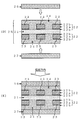
まず、図3及び図4を参照しながら第一の態様の微細配線付透明樹脂基材10について説明する。第一の態様の微細配線付透明樹脂基材10は、透明樹脂基材11の片面に、銅箔12aの片面に微細凹凸構造層12bを備えた透明樹脂基材用銅箔12を張り合わせた後(図3(A)参照)、エッチング法により配線パターンを形成することにより得られたもので、図3(B)に示すように、透明樹脂基材11の片面11aに線幅が10μm以下の銅配線13が複数設けられている。図3(B)に示す例では、銅配線13は、銅箔層12aの片面に設けられた微細凹凸構造層12bを介して透明樹脂基材11に密着している。これらの透明樹脂基材11及び微細凹凸構造層12bは、上述した透明樹脂基材用銅箔において説明した透明樹脂基材及び微細凹凸構造層と同様の構成等を有し、銅箔層12aは上述した銅箔と同様の構成等を有する。従って、第一の態様において、これらに関して、上記と重複する内容の説明を省略するが、これらは上記と同様の構成等を有する以上、上記と同様の機能及び効果を発現するのは勿論である。
まず、図3及び図4を参照しながら第一の態様の微細配線付透明樹脂基材10について説明する。第一の態様の微細配線付透明樹脂基材10は、透明樹脂基材11の片面に、銅箔12aの片面に微細凹凸構造層12bを備えた透明樹脂基材用銅箔12を張り合わせた後(図3(A)参照)、エッチング法により配線パターンを形成することにより得られたもので、図3(B)に示すように、透明樹脂基材11の片面11aに線幅が10μm以下の銅配線13が複数設けられている。図3(B)に示す例では、銅配線13は、銅箔層12aの片面に設けられた微細凹凸構造層12bを介して透明樹脂基材11に密着している。これらの透明樹脂基材11及び微細凹凸構造層12bは、上述した透明樹脂基材用銅箔において説明した透明樹脂基材及び微細凹凸構造層と同様の構成等を有し、銅箔層12aは上述した銅箔と同様の構成等を有する。従って、第一の態様において、これらに関して、上記と重複する内容の説明を省略するが、これらは上記と同様の構成等を有する以上、上記と同様の機能及び効果を発現するのは勿論である。
第一の態様では、銅配線13が備える微細凹凸構造層12bは、透明樹脂基材11と銅箔層12aとを密着させるための密着層として機能する。微細凹凸構造層12bは透明樹脂基材11に張り合わされる際に、透明樹脂基材11を構成する樹脂材料が熱により溶融硬化する過程で、その針状又は板状の凸状部が透明樹脂基材11の内部に埋まり込んだ状態となり、透明樹脂基材11と銅箔層12aとはこの微細凹凸構造層12bにより良好な密着性を有する。
また、透明樹脂基材11の他面11b側から可視光が入射すると、透明樹脂基材11を透過した可視光は透明樹脂基材11の片面11a側に設けられた銅配線13の微細凹凸構造層12bに入射する。この場合、微細凹凸構造層12bは上述したとおり反射防止層としても機能するため、この入射光の反射を抑制する。例えば、透明樹脂基材11の片面11aに、片面11aの露出部分及び銅配線13を被覆するように、透明光学粘着フィルム層(以下、OCA層)14を設けて一組の電極材15とする(図3(C)参照)。これを二組用意し、図4(D)に示すように、一方の電極部材15のOCA層14の表面に他の電極部材15の透明樹脂基材11の他面11b側が密着するようにこれらを積層することにより、タッチパネル等の微細配線型透明電極を得ることができる。そして、銅配線13の微細凹凸構造層12bが設けられた側をユーザーからの視認側とし、一方の電極部材15の透明樹脂基材11の他面11b側の面にカバーガラス16を設け、他方の電極部材15のOCA層14の表面に更に別の透明樹脂基材17を積層することにより、静電容量式のタッチパネルとすることができる。
上記第一の態様によれば、銅配線13において、ユーザーからの視認側に微細凹凸構造層12bが設けられているため、銅配線13に入射する光の反射を防止することができ、ディスプレイに表示される画像のコントラストの低下等を防止して、画質の低下を防ぐことができる。さらに、ユーザーからの視認側に微細凹凸構造層12bが設けられているため、配線パターン形成後に改めて黒化処理を施す必要がない。このため、線幅10μm以下、好ましくは線幅6μm以下の極微細な銅配線についても良好に形成することができる。
また、当該微細配線付透明樹脂基材10を用いて、図4(E)に示すタッチパネルを製造した場合、微細凹凸構造層12bにより透明樹脂基材11と銅配線13とを良好に密着させることができる。ここで、ユーザーがタッチパネルを押下した場合、透明樹脂基材11が撓み、透明樹脂基材11と銅配線13との間に応力が負荷される。タッチパネルの操作が繰り返し行われると、透明樹脂基材11と銅配線13との間にも応力が繰り返し負荷される。しかしながら、第一の態様では、上述のとおり、微細凹凸構造層12bを介して透明樹脂基材11と銅配線13とを密着させているため、両者の間に応力が繰り返し負荷されても銅配線13が透明樹脂基材11から剥離するのを防止することができる。
ここで、上述した第一の態様の微細配線付透明樹脂基材10は、銅箔層12aの片面にのみ微細凹凸構造層12bが設けられているが、第一の態様において銅箔層12aの両面に微細凹凸構造層12bを設けてもよい。この場合、その後、図3(A)において、銅箔12aの両面に微細凹凸構造層12bを備えた透明樹脂基材用銅箔を透明樹脂基材11に張り合わせて、図3(A)と同様の積層体を得た後、図3(B)と同様にエッチング法により配線パターンを形成すれば、銅箔層12aの両面に微細凹凸構造層12bを備えた銅配線13を得ることができる。銅箔層12aの両面に微細凹凸構造層12bを設ければ、銅配線13と透明樹脂基材11との間だけではなく、銅配線13とOCA層14との間を微細凹凸構造層12bを介して良好に密着させることができる。従って、タッチパネルが繰り返し操作された場合にも、銅配線13と透明樹脂基材11との密着性を維持すると共に、銅配線13とOCA層14との密着性を維持することができる。
また、第一の態様の当該微細銅配線付透明樹脂基材10では、エッチング法により銅配線13が形成されるため、銅配線13の側面では銅箔層が露出している。従って、当該微細配線付透明樹脂基材10を用いて、タッチパネル等の微細配線型透明電極を製造した場合、ユーザーの視認方向によっては、この銅箔層12aの側面に入射した可視光の反射光により、コントラストが低下する場合がある。従って、銅箔層12aの厚みは、銅箔層12aの側面における入射光の鏡面反射を抑制するという観点からも、当該銅箔層12aの厚みは薄い方が好ましく、12μm以下であることがより好ましい。銅箔層12aの厚みは、上述した銅箔の厚みと同様であり、銅箔層12aの厚みが薄い方が良好なエッチングファクタで銅配線13を形成する上でも好ましい。
(2)第二の態様
次に、図5及び図6を参照しながら第二の態様の微細配線付透明樹脂基材20について説明する。第二の態様の微細配線付透明樹脂基材20は、図5(A)に示すように、透明樹脂基材21の両面に、銅箔22aの両面に微細凹凸構造層22bを備えた透明樹脂基材用銅箔22を張り合わせた後、エッチング法により透明樹脂基材21の両面に配線パターンを形成することにより得られたもので、図5(B)に示すように、透明樹脂基材21の両面に、それぞれ線幅が10μm以下の銅配線22が複数設けられている。ここで、透明樹脂基材21、銅配線23、銅箔層22a、微細凹凸構造層22b及び透明樹脂基材用銅箔22は、それぞれ上述した透明樹脂基材用銅箔又は第一の態様の微細配線付透明樹脂基材10において説明した透明樹脂基材11、銅配線13、銅箔層12a、微細凹凸構造層12b及び透明樹脂基材用銅箔12と同様の構成を有するため、上記と重複する内容の説明を省略する。しかしながら、これらは上記と同様の構成を有する以上、同様の機能及び効果を発現するのは勿論である。
次に、図5及び図6を参照しながら第二の態様の微細配線付透明樹脂基材20について説明する。第二の態様の微細配線付透明樹脂基材20は、図5(A)に示すように、透明樹脂基材21の両面に、銅箔22aの両面に微細凹凸構造層22bを備えた透明樹脂基材用銅箔22を張り合わせた後、エッチング法により透明樹脂基材21の両面に配線パターンを形成することにより得られたもので、図5(B)に示すように、透明樹脂基材21の両面に、それぞれ線幅が10μm以下の銅配線22が複数設けられている。ここで、透明樹脂基材21、銅配線23、銅箔層22a、微細凹凸構造層22b及び透明樹脂基材用銅箔22は、それぞれ上述した透明樹脂基材用銅箔又は第一の態様の微細配線付透明樹脂基材10において説明した透明樹脂基材11、銅配線13、銅箔層12a、微細凹凸構造層12b及び透明樹脂基材用銅箔12と同様の構成を有するため、上記と重複する内容の説明を省略する。しかしながら、これらは上記と同様の構成を有する以上、同様の機能及び効果を発現するのは勿論である。
第二の態様の微細配線付透明樹脂基材20では、透明樹脂基材21の両面に銅配線23が設けられているため、この状態で微細配線型透明電極とすることができる。次に、この両面にそれぞれ第一の態様と同様にOCA層24を設け(図5(C)参照)、このOCA層24が設けられた積層体25において、ユーザーからの視認側となる側のOCA層24の表面にカバーガラス26を設け、他面側のOCA層24の表面に更に別の透明樹脂基材27を積層することにより、静電容量式のタッチパネルとすることができる。
この第二の態様では、透明樹脂基材21の両面に銅配線23を設けることにより、微細配線型透明電極としたときに、第一の態様の微細配線型透明電極とは異なり、透明樹脂基材21の層を一層削減することができる。このため、第二の態様の微細配線型透明電極における可視光の透過率を第一の態様の微細配線型透明電極よりも高くすることができる。また、第二の態様の微細配線型電極は、第一の態様の微細配線型電極と比較すると、透明樹脂基材21の積層数が少なくなるため、工程及びコストを低減することができる。
また、第二の態様においては、透明樹脂基材21の両面に、両面に微細凹凸構造層22b2を備えた銅配線23を設けている。このため、当該微細配線型樹脂基材20を用いれば、いずれの面をユーザーからの視認側としても、銅配線23に入射する光の反射を防止することができる。また、いずれの面をユーザーからの視認側としても、銅配線23のユーザーからの視認側には微細凹凸構造層22bが設けられているため、配線パターン形成後に黒化処理を施す必要がない。
但し、銅配線23に対する入射光の反射を防止するという観点からは、透明樹脂基材21のユーザーからの視認側とは反対側の面に設ける銅配線23については、透明樹脂基材21との張り合わせ面にのみ微細凹凸構造層22bを備えた銅配線23とすれば足りる。しかしながら、第一の態様において述べたとおり、ユーザーからの視認側とは反対側の面に設ける銅配線23についても、その両面に微細凹凸構造層22bを設けることにより、透明樹脂基材21とだけではなく、OCA層24とも密着性の良好な銅配線とすることができる。
以下、本願発明に係る透明樹脂基材用銅箔の実施例について説明するが、本願発明に係る透明樹脂基材用銅箔は以下の実施例に限定されるものではなく、本願発明の趣旨を逸脱しない範囲において適宜変更可能であるのは勿論である。
実施例では、以下に記載した組成の銅電解液を用い、陽極にDSA、陰極(表面を2000番の研磨紙で研磨したチタン板電極)を用い、液温50℃、電流密度60A/dm2の条件で電解して、18μm厚さの電解銅箔を得た。そして、以下の手順で、電解銅箔の両面に微細凹凸構造層を形成し、本願発明に係る透明樹脂基材用銅箔とした。
〔銅電解液組成〕
銅濃度 : 80g/L
フリー硫酸濃度 : 140g/L
ビス(3-スルホプロピル)ジスルフィド濃度 : 5mg/L
ジアリルジメチルアンモニウムクロライド重合体濃度 : 30mg/L
塩素濃度 : 25mg/L
銅濃度 : 80g/L
フリー硫酸濃度 : 140g/L
ビス(3-スルホプロピル)ジスルフィド濃度 : 5mg/L
ジアリルジメチルアンモニウムクロライド重合体濃度 : 30mg/L
塩素濃度 : 25mg/L
予備処理: 当該電解銅箔を、水酸化ナトリウム水溶液に浸漬して、アルカリ脱脂処理を行い、水洗を行った。そして、このアルカリ脱脂処理の終了した電解銅箔を、過酸化水素濃度が1質量%、硫酸濃度が5質量%の硫酸系溶液に5分間浸漬した後、水洗を行った。
酸化処理: 上記予備処理の終了した電解銅箔を、液温70℃、pH=12、亜塩素酸濃度が150g/L、N-2-(アミノエチル)-3-アミノプロピルトリメトキシシラン濃度が10g/Lを含む水酸化ナトリウム溶液に、所定の酸化処理時間(1分間、2分間、4分間、10分間)浸漬して、電解銅箔の両面に酸化処理を施して、酸化処理時間の異なる4種類の試料を得た。
還元処理: 酸化処理の終了した各試料について、炭酸ナトリウムと水酸化ナトリウムを用いてpH=12に調整したジメチルアミンボラン濃度が20g/Lの水溶液(室温)中に1分間浸漬して還元処理を行い、水洗し、乾燥して、電解銅箔の両面に、銅複合化合物からなる最大長さが500nm以下の針状又は板状の凸状部により形成された微細凹凸構造を有する微細凹凸構造層を形成した。この微細凹凸構造を形成する凸状部の先端部分の長さを当該凸状部の最大長さと共に表1に示す。なお、当該凸状部の最大長さ及び先端部分の長さは、上述したとおりである。
当該実施例で得られた透明樹脂基材用銅箔の微細凹凸構造層の表面をXPSを用いて状態分析をすると、「Cu(I)」、「Cu(II)」及び「-COO基」の存在が確認された。更に、この実施例で得られた透明樹脂基材用銅箔のCu(I)ピークの占有面積率、比表面積及び明度(L*値)を以下の表1に示す。
比較例では、実施例と同じ電解銅箔を用い、実施例と同様に予備処理を行った後、以下の条件で電解銅箔の両面に黒化処理を施し、これを比較例の透明樹脂基材用銅箔とした。
黒化処理: ローム・アンド・ハース電子材料株式会社製の酸化処理液である「PRO BOND 80A OXIDE SOLUTION」10vol%、「PRO BOND 80B OXIDE SOLUTION」20vol%含有する液温85℃の水溶液に上記予備処理の終了した電解銅箔を5分間浸漬し、黒化処理を施した。当該黒化処理により銅箔表面に形成された凸状部(針状結晶)の最大長さ及び先端部分の長さを表1に示す。
当該比較例で得られた透明樹脂基材用銅箔の黒化処理層の表面をXPSを用いて状態分析をした。当該黒化処理層では「Cu(I)」、「Cu(II)」の存在は確認されたが、「-COO基」の存在は確認されなかった。更に、この比較例で得られた透明樹脂基材用銅箔のCu(I)ピークの占有面積率、比表面積及び明度(L*値)を表1に示す。

本願発明によれば、透明樹脂基材用銅箔は、銅箔の表面に酸化第一銅及び酸化第二銅を含み、これら銅複合化合物からなる最大長さが500nm以下の針状又は板状の凸状部により形成された微細凹凸構造を有する微細凹凸構造層を備えている。すなわち、当該微細凹凸構造は、最大長さが500nm以下の針状又は板状の凸状部により形成されており、銅箔の表面から長く突出する針状又は板状の凸状部が存在しない。このため、当該微細凹凸構造層の表面に他の物体が接触したとしても、これらの針状又は板状の凸状部は短いため、折れにくく、耐擦傷性が高い。従って、当該透明樹脂基材用銅箔は、ハンドリングの際等にいわゆる粉落ちが生じにくく、表面の微細凹凸構造を維持することができ、周囲に酸化銅の微粉が飛散したり、付着するのを防止することができる。従って、当該透明樹脂基材用銅箔を用いて、タッチパネル等の微細配線型透明電極を製造した場合、粉落ちに起因した反射防止効果のムラや、配線間の絶縁不良を生じにくくすることができる。このため、銅箔の両面に当該微細凹凸構造層を設けることも容易になる。
また、本願発明において、当該微細凹凸構造層は、酸化第一銅及び酸化第二銅を含むため、従来の黒色酸化銅被膜と比較すると、酸化第一銅を含有する比率に応じて、エッチング液等に対する耐酸溶解性を向上することができる。従って、微細凹凸構造層側を透明樹脂基材側に張り合わせて、エッチング法により銅配線を形成する際に微細凹凸構造層が溶解して、透明樹脂基材と銅配線との密着性が低下するのを抑制することができる。
さらに、当該微細凹凸構造は最大長さが500nm以下の針状又は板状の凸状部からなるため、凸状部間の最大ピッチは可視光の波長域よりも短くなる傾向にある。最大ピッチが可視光の波長域以下である場合、当該微細凹凸構造層に入射した可視光の表面反射率を極めて小さくすることができ、高い反射防止機能を有する層とすることができる。
さらに、本願発明に係る透明樹脂基材用銅箔において、銅箔の両面に当該微細凹凸構造層を設けた場合、両面が暗褐色~黒色の両面黒色銅箔とすることができる。これを利用すれば、銅箔の片面側に設けられた微細凹凸構造層により、透明樹脂基材との密着性を担保すると共に、銅箔の他面側に設けられた微細凹凸構造層により銅箔の他面側に入射した可視光の鏡面反射を抑制することができる。つまり、両面に微細凹凸構造層を備えた銅箔を用いて、上記微細配線型透明電極を製造すれば、透明樹脂基材との密着性が良好であり、且つ、透明樹脂基材側及びその反対側のいずれにも高い反射防止機能を有する層を備えた銅配線を形成することができる。
Claims (10)
- 透明樹脂基材の表面に銅配線を形成するための透明樹脂基材用銅箔であって、
銅箔の表面に、酸化第一銅及び酸化第二銅を含み、これら銅複合化合物からなる最大長さが500nm以下の針状又は板状の凸状部により形成された微細凹凸構造を有する微細凹凸構造層を備えたこと、
を特徴とする透明樹脂基材用銅箔。 - X線光電子分光分析法により前記微細凹凸構造層の構成元素を分析したときに得られるCu(I)のピーク面積と、Cu(II)のピーク面積との合計面積に対して、Cu(I)のピーク面積が占める割合が50%以上である請求項1に記載の透明樹脂基材用銅箔。
- 前記微細凹凸構造層の表面のCIE-L*a*b*表色系におけるL*値が30以下である請求項1又は請求項2に記載の透明樹脂基材用銅箔。
- 走査型電子顕微鏡を用いて、傾斜角45°、50000倍以上の倍率で前記微細凹凸構造層の表面を観察したときに、互いに隣接する凸状部のうち、他の凸状部と分離観察可能な先端部分の長さが250nm以下である請求項1~請求項3のいずれか一項に記載の透明樹脂基材用銅箔。
- 前記凸状部の前記最大長さに対して、前記凸状部の前記先端部分の長さが1/2以下である請求項4に記載の透明樹脂基材用銅箔。
- 前記銅箔の両面に前記微細凹凸構造層を備える請求項1~請求項5のいずれか一項に記載の透明樹脂基材用銅箔。
- 透明樹脂基材の表面に、線幅が10μm以下の銅配線が設けられた微細銅配線付透明樹脂基材であって、
当該銅配線は、銅箔層と、酸化第一銅及び酸化第二銅を含み、これら銅複合化合物からなる最大長さが500nm以下の針状又は板状の凸状部により形成された微細凹凸構造を有する微細凹凸構造層とを備えたこと、
を特徴とする微細銅配線付透明樹脂基材。 - 前記銅配線は、前記微細凹凸構造層を介して透明樹脂基材の表面に密着されている請求項7に記載の微細銅配線付透明樹脂基材。
- 前記微細凹凸構造層が、前記銅箔層の前記透明樹脂基材との密着面とは反対側の面に設けられている請求項7又は請求項8に記載の微細銅配線付透明樹脂基材。
- 前記銅配線の側面において、前記銅箔層の断面が露出している請求項7~請求項9のいずれか一項に記載の微細銅配線付樹脂基材。
Priority Applications (1)
| Application Number | Priority Date | Filing Date | Title |
|---|---|---|---|
| JP2015527607A JPWO2015178455A1 (ja) | 2014-05-21 | 2015-05-21 | 透明樹脂基材用銅箔及び微細銅配線付透明樹脂基材 |
Applications Claiming Priority (2)
| Application Number | Priority Date | Filing Date | Title |
|---|---|---|---|
| JP2014-105579 | 2014-05-21 | ||
| JP2014105579 | 2014-05-21 |
Publications (1)
| Publication Number | Publication Date |
|---|---|
| WO2015178455A1 true WO2015178455A1 (ja) | 2015-11-26 |
Family
ID=54554116
Family Applications (1)
| Application Number | Title | Priority Date | Filing Date |
|---|---|---|---|
| PCT/JP2015/064630 Ceased WO2015178455A1 (ja) | 2014-05-21 | 2015-05-21 | 透明樹脂基材用銅箔及び微細銅配線付透明樹脂基材 |
Country Status (3)
| Country | Link |
|---|---|
| JP (1) | JPWO2015178455A1 (ja) |
| TW (1) | TW201544309A (ja) |
| WO (1) | WO2015178455A1 (ja) |
Cited By (1)
| Publication number | Priority date | Publication date | Assignee | Title |
|---|---|---|---|---|
| JP2018016886A (ja) * | 2016-07-15 | 2018-02-01 | ナミックス株式会社 | プリント配線板に用いる銅箔の製造方法 |
Families Citing this family (1)
| Publication number | Priority date | Publication date | Assignee | Title |
|---|---|---|---|---|
| CN116034632A (zh) * | 2020-11-02 | 2023-04-28 | 纳美仕有限公司 | 多层基板用布线及其制造方法 |
Citations (5)
| Publication number | Priority date | Publication date | Assignee | Title |
|---|---|---|---|---|
| JPS56153797A (en) * | 1980-04-28 | 1981-11-27 | Hitachi Chemical Co Ltd | Method of manufacturing multilayer printed circuit board substrate |
| JP2006021455A (ja) * | 2004-07-09 | 2006-01-26 | Mitsui Chemicals Inc | ポリイミド金属積層体 |
| JP2008248269A (ja) * | 2007-03-29 | 2008-10-16 | Hitachi Chem Co Ltd | 銅表面の処理方法およびこの方法を用いた配線基板 |
| JP2011174132A (ja) * | 2010-02-24 | 2011-09-08 | Hitachi Cable Ltd | プリント配線板用銅箔 |
| WO2013176133A1 (ja) * | 2012-05-21 | 2013-11-28 | Jx日鉱日石金属株式会社 | 表面処理銅箔及びそれを用いた積層板、プリント配線板、電子機器及びプリント配線板を製造する方法 |
-
2015
- 2015-05-21 WO PCT/JP2015/064630 patent/WO2015178455A1/ja not_active Ceased
- 2015-05-21 JP JP2015527607A patent/JPWO2015178455A1/ja active Pending
- 2015-05-21 TW TW104116279A patent/TW201544309A/zh unknown
Patent Citations (5)
| Publication number | Priority date | Publication date | Assignee | Title |
|---|---|---|---|---|
| JPS56153797A (en) * | 1980-04-28 | 1981-11-27 | Hitachi Chemical Co Ltd | Method of manufacturing multilayer printed circuit board substrate |
| JP2006021455A (ja) * | 2004-07-09 | 2006-01-26 | Mitsui Chemicals Inc | ポリイミド金属積層体 |
| JP2008248269A (ja) * | 2007-03-29 | 2008-10-16 | Hitachi Chem Co Ltd | 銅表面の処理方法およびこの方法を用いた配線基板 |
| JP2011174132A (ja) * | 2010-02-24 | 2011-09-08 | Hitachi Cable Ltd | プリント配線板用銅箔 |
| WO2013176133A1 (ja) * | 2012-05-21 | 2013-11-28 | Jx日鉱日石金属株式会社 | 表面処理銅箔及びそれを用いた積層板、プリント配線板、電子機器及びプリント配線板を製造する方法 |
Cited By (1)
| Publication number | Priority date | Publication date | Assignee | Title |
|---|---|---|---|---|
| JP2018016886A (ja) * | 2016-07-15 | 2018-02-01 | ナミックス株式会社 | プリント配線板に用いる銅箔の製造方法 |
Also Published As
| Publication number | Publication date |
|---|---|
| TW201544309A (zh) | 2015-12-01 |
| JPWO2015178455A1 (ja) | 2017-04-20 |
Similar Documents
| Publication | Publication Date | Title |
|---|---|---|
| JP5809361B2 (ja) | 表面処理銅箔及び表面処理銅箔を用いて得られる銅張積層板 | |
| JP2017048467A (ja) | 銅箔、キャリア箔付銅箔及び銅張積層板 | |
| CN107109679B (zh) | 印刷线路板用表面处理铜箔、印刷线路板用覆铜层压板及印刷线路板 | |
| US20160229154A1 (en) | Touch-sensitive panel device and electrode structure therein | |
| WO2013108414A1 (ja) | 銅張積層板用表面処理銅箔及びそれを用いた銅張積層板 | |
| KR101931895B1 (ko) | 고주파 신호 전송 회로 형성용 표면 처리 동박, 동장 적층판 및 프린트 배선판 | |
| CN105934307A (zh) | 粗化处理铜箔、覆铜层压板以及印刷线路板 | |
| CN104364426A (zh) | 表面处理铜箔及使用其的积层板、印刷配线板、电子机器、以及印刷配线板的制造方法 | |
| JP7122675B2 (ja) | 金属基材付薄膜金属箔、金属張透明基材材料、透視型電極用積層板、透視型電極素材、及びデバイス | |
| CN106103082A (zh) | 带有载体箔的铜箔、覆铜层压板及印刷线路板 | |
| JP6445365B2 (ja) | 透視性電極、該透視性電極を用いてなるタッチパネル用位置検知電極、タッチパネル、及び画像表示装置 | |
| JPWO2006090798A1 (ja) | 電磁波遮蔽積層体およびこれを用いたディスプレイ装置 | |
| JP2008227352A (ja) | 電磁波遮蔽シート、その製造方法、及びプラズマディスプレイパネル用フィルター | |
| CN103857178B (zh) | 具有黑色极薄铜箔的铜箔结构及其制造方法 | |
| JP2015157392A (ja) | 透視型電極用積層体とその製造方法、透視型電極素材とデバイス | |
| WO2015178455A1 (ja) | 透明樹脂基材用銅箔及び微細銅配線付透明樹脂基材 | |
| TWI593325B (zh) | Circuit board | |
| CN109696999A (zh) | 带金属基材的薄膜金属箔、覆金属透明基材材料、透视型电极用层叠板、电极原材及器件 | |
| JP2019019351A (ja) | 剥離金属基材付薄膜銅箔及びその製造方法 | |
| TWI791428B (zh) | 黑化鍍液、導電性基板的製造方法 | |
| JP6500746B2 (ja) | 導電性基板の製造方法 | |
| TW201710564A (zh) | 黑化鍍液、導電性基板 | |
| TWI791429B (zh) | 黑化鍍液、導電性基板之製造方法 | |
| JPWO2005067362A1 (ja) | 電磁波シールドフィルタ用銅箔及び電磁波シールドフィルタ | |
| JP2021014623A (ja) | 金属基材付薄膜金属箔、金属張透明基材材料、透視型電極用積層板、及び透視型電極素材 |
Legal Events
| Date | Code | Title | Description |
|---|---|---|---|
| ENP | Entry into the national phase |
Ref document number: 2015527607 Country of ref document: JP Kind code of ref document: A |
|
| 121 | Ep: the epo has been informed by wipo that ep was designated in this application |
Ref document number: 15796527 Country of ref document: EP Kind code of ref document: A1 |
|
| NENP | Non-entry into the national phase |
Ref country code: DE |
|
| 122 | Ep: pct application non-entry in european phase |
Ref document number: 15796527 Country of ref document: EP Kind code of ref document: A1 |