WO2015174158A1 - パワー半導体モジュールおよび複合モジュール - Google Patents
パワー半導体モジュールおよび複合モジュール Download PDFInfo
- Publication number
- WO2015174158A1 WO2015174158A1 PCT/JP2015/060340 JP2015060340W WO2015174158A1 WO 2015174158 A1 WO2015174158 A1 WO 2015174158A1 JP 2015060340 W JP2015060340 W JP 2015060340W WO 2015174158 A1 WO2015174158 A1 WO 2015174158A1
- Authority
- WO
- WIPO (PCT)
- Prior art keywords
- power semiconductor
- lid
- semiconductor module
- resin
- circuit board
- Prior art date
- Legal status (The legal status is an assumption and is not a legal conclusion. Google has not performed a legal analysis and makes no representation as to the accuracy of the status listed.)
- Ceased
Links
Images

Classifications
-
- H—ELECTRICITY
- H10—SEMICONDUCTOR DEVICES; ELECTRIC SOLID-STATE DEVICES NOT OTHERWISE PROVIDED FOR
- H10W—GENERIC PACKAGES, INTERCONNECTIONS, CONNECTORS OR OTHER CONSTRUCTIONAL DETAILS OF DEVICES COVERED BY CLASS H10
- H10W90/00—Package configurations
-
- H—ELECTRICITY
- H10—SEMICONDUCTOR DEVICES; ELECTRIC SOLID-STATE DEVICES NOT OTHERWISE PROVIDED FOR
- H10W—GENERIC PACKAGES, INTERCONNECTIONS, CONNECTORS OR OTHER CONSTRUCTIONAL DETAILS OF DEVICES COVERED BY CLASS H10
- H10W40/00—Arrangements for thermal protection or thermal control
- H10W40/60—Securing means for detachable heating or cooling arrangements, e.g. clamps
- H10W40/611—Bolts or screws
-
- H—ELECTRICITY
- H10—SEMICONDUCTOR DEVICES; ELECTRIC SOLID-STATE DEVICES NOT OTHERWISE PROVIDED FOR
- H10W—GENERIC PACKAGES, INTERCONNECTIONS, CONNECTORS OR OTHER CONSTRUCTIONAL DETAILS OF DEVICES COVERED BY CLASS H10
- H10W70/00—Package substrates; Interposers; Redistribution layers [RDL]
- H10W70/20—Conductive package substrates serving as an interconnection, e.g. metal plates
- H10W70/24—Conductive package substrates serving as an interconnection, e.g. metal plates characterised by materials
-
- H—ELECTRICITY
- H10—SEMICONDUCTOR DEVICES; ELECTRIC SOLID-STATE DEVICES NOT OTHERWISE PROVIDED FOR
- H10W—GENERIC PACKAGES, INTERCONNECTIONS, CONNECTORS OR OTHER CONSTRUCTIONAL DETAILS OF DEVICES COVERED BY CLASS H10
- H10W70/00—Package substrates; Interposers; Redistribution layers [RDL]
- H10W70/60—Insulating or insulated package substrates; Interposers; Redistribution layers
- H10W70/611—Insulating or insulated package substrates; Interposers; Redistribution layers for connecting multiple chips together
-
- H—ELECTRICITY
- H10—SEMICONDUCTOR DEVICES; ELECTRIC SOLID-STATE DEVICES NOT OTHERWISE PROVIDED FOR
- H10W—GENERIC PACKAGES, INTERCONNECTIONS, CONNECTORS OR OTHER CONSTRUCTIONAL DETAILS OF DEVICES COVERED BY CLASS H10
- H10W70/00—Package substrates; Interposers; Redistribution layers [RDL]
- H10W70/60—Insulating or insulated package substrates; Interposers; Redistribution layers
- H10W70/62—Insulating or insulated package substrates; Interposers; Redistribution layers characterised by their interconnections
- H10W70/65—Shapes or dispositions of interconnections
-
- H—ELECTRICITY
- H10—SEMICONDUCTOR DEVICES; ELECTRIC SOLID-STATE DEVICES NOT OTHERWISE PROVIDED FOR
- H10W—GENERIC PACKAGES, INTERCONNECTIONS, CONNECTORS OR OTHER CONSTRUCTIONAL DETAILS OF DEVICES COVERED BY CLASS H10
- H10W70/00—Package substrates; Interposers; Redistribution layers [RDL]
- H10W70/60—Insulating or insulated package substrates; Interposers; Redistribution layers
- H10W70/62—Insulating or insulated package substrates; Interposers; Redistribution layers characterised by their interconnections
- H10W70/65—Shapes or dispositions of interconnections
- H10W70/657—Shapes or dispositions of interconnections on sidewalls or bottom surfaces of the package substrates, interposers or redistribution layers
-
- H—ELECTRICITY
- H10—SEMICONDUCTOR DEVICES; ELECTRIC SOLID-STATE DEVICES NOT OTHERWISE PROVIDED FOR
- H10W—GENERIC PACKAGES, INTERCONNECTIONS, CONNECTORS OR OTHER CONSTRUCTIONAL DETAILS OF DEVICES COVERED BY CLASS H10
- H10W72/00—Interconnections or connectors in packages
-
- H—ELECTRICITY
- H10—SEMICONDUCTOR DEVICES; ELECTRIC SOLID-STATE DEVICES NOT OTHERWISE PROVIDED FOR
- H10W—GENERIC PACKAGES, INTERCONNECTIONS, CONNECTORS OR OTHER CONSTRUCTIONAL DETAILS OF DEVICES COVERED BY CLASS H10
- H10W72/00—Interconnections or connectors in packages
- H10W72/50—Bond wires
-
- H—ELECTRICITY
- H10—SEMICONDUCTOR DEVICES; ELECTRIC SOLID-STATE DEVICES NOT OTHERWISE PROVIDED FOR
- H10W—GENERIC PACKAGES, INTERCONNECTIONS, CONNECTORS OR OTHER CONSTRUCTIONAL DETAILS OF DEVICES COVERED BY CLASS H10
- H10W74/00—Encapsulations, e.g. protective coatings
- H10W74/10—Encapsulations, e.g. protective coatings characterised by their shape or disposition
- H10W74/111—Encapsulations, e.g. protective coatings characterised by their shape or disposition the semiconductor body being completely enclosed
- H10W74/114—Encapsulations, e.g. protective coatings characterised by their shape or disposition the semiconductor body being completely enclosed by a substrate and the encapsulations
-
- H—ELECTRICITY
- H10—SEMICONDUCTOR DEVICES; ELECTRIC SOLID-STATE DEVICES NOT OTHERWISE PROVIDED FOR
- H10W—GENERIC PACKAGES, INTERCONNECTIONS, CONNECTORS OR OTHER CONSTRUCTIONAL DETAILS OF DEVICES COVERED BY CLASS H10
- H10W76/00—Containers; Fillings or auxiliary members therefor; Seals
- H10W76/10—Containers or parts thereof
- H10W76/12—Containers or parts thereof characterised by their shape
- H10W76/13—Containers comprising a conductive base serving as an interconnection
- H10W76/136—Containers comprising a conductive base serving as an interconnection having other interconnections perpendicular to the conductive base
-
- H—ELECTRICITY
- H10—SEMICONDUCTOR DEVICES; ELECTRIC SOLID-STATE DEVICES NOT OTHERWISE PROVIDED FOR
- H10W—GENERIC PACKAGES, INTERCONNECTIONS, CONNECTORS OR OTHER CONSTRUCTIONAL DETAILS OF DEVICES COVERED BY CLASS H10
- H10W76/00—Containers; Fillings or auxiliary members therefor; Seals
- H10W76/10—Containers or parts thereof
- H10W76/12—Containers or parts thereof characterised by their shape
- H10W76/15—Containers comprising an insulating or insulated base
-
- H—ELECTRICITY
- H10—SEMICONDUCTOR DEVICES; ELECTRIC SOLID-STATE DEVICES NOT OTHERWISE PROVIDED FOR
- H10W—GENERIC PACKAGES, INTERCONNECTIONS, CONNECTORS OR OTHER CONSTRUCTIONAL DETAILS OF DEVICES COVERED BY CLASS H10
- H10W76/00—Containers; Fillings or auxiliary members therefor; Seals
- H10W76/40—Fillings or auxiliary members in containers, e.g. centering rings
-
- H—ELECTRICITY
- H10—SEMICONDUCTOR DEVICES; ELECTRIC SOLID-STATE DEVICES NOT OTHERWISE PROVIDED FOR
- H10W—GENERIC PACKAGES, INTERCONNECTIONS, CONNECTORS OR OTHER CONSTRUCTIONAL DETAILS OF DEVICES COVERED BY CLASS H10
- H10W90/00—Package configurations
- H10W90/401—Package configurations characterised by multiple insulating or insulated package substrates, interposers or RDLs
-
- H—ELECTRICITY
- H10—SEMICONDUCTOR DEVICES; ELECTRIC SOLID-STATE DEVICES NOT OTHERWISE PROVIDED FOR
- H10W—GENERIC PACKAGES, INTERCONNECTIONS, CONNECTORS OR OTHER CONSTRUCTIONAL DETAILS OF DEVICES COVERED BY CLASS H10
- H10W40/00—Arrangements for thermal protection or thermal control
- H10W40/20—Arrangements for cooling
- H10W40/22—Arrangements for cooling characterised by their shape, e.g. having conical or cylindrical projections
-
- H—ELECTRICITY
- H10—SEMICONDUCTOR DEVICES; ELECTRIC SOLID-STATE DEVICES NOT OTHERWISE PROVIDED FOR
- H10W—GENERIC PACKAGES, INTERCONNECTIONS, CONNECTORS OR OTHER CONSTRUCTIONAL DETAILS OF DEVICES COVERED BY CLASS H10
- H10W40/00—Arrangements for thermal protection or thermal control
- H10W40/20—Arrangements for cooling
- H10W40/25—Arrangements for cooling characterised by their materials
- H10W40/255—Arrangements for cooling characterised by their materials having a laminate or multilayered structure, e.g. direct bond copper [DBC] ceramic substrates
-
- H—ELECTRICITY
- H10—SEMICONDUCTOR DEVICES; ELECTRIC SOLID-STATE DEVICES NOT OTHERWISE PROVIDED FOR
- H10W—GENERIC PACKAGES, INTERCONNECTIONS, CONNECTORS OR OTHER CONSTRUCTIONAL DETAILS OF DEVICES COVERED BY CLASS H10
- H10W40/00—Arrangements for thermal protection or thermal control
- H10W40/60—Securing means for detachable heating or cooling arrangements, e.g. clamps
-
- H—ELECTRICITY
- H10—SEMICONDUCTOR DEVICES; ELECTRIC SOLID-STATE DEVICES NOT OTHERWISE PROVIDED FOR
- H10W—GENERIC PACKAGES, INTERCONNECTIONS, CONNECTORS OR OTHER CONSTRUCTIONAL DETAILS OF DEVICES COVERED BY CLASS H10
- H10W70/00—Package substrates; Interposers; Redistribution layers [RDL]
- H10W70/40—Leadframes
- H10W70/479—Leadframes on or in insulating or insulated package substrates, interposers, or redistribution layers
-
- H—ELECTRICITY
- H10—SEMICONDUCTOR DEVICES; ELECTRIC SOLID-STATE DEVICES NOT OTHERWISE PROVIDED FOR
- H10W—GENERIC PACKAGES, INTERCONNECTIONS, CONNECTORS OR OTHER CONSTRUCTIONAL DETAILS OF DEVICES COVERED BY CLASS H10
- H10W70/00—Package substrates; Interposers; Redistribution layers [RDL]
- H10W70/60—Insulating or insulated package substrates; Interposers; Redistribution layers
- H10W70/62—Insulating or insulated package substrates; Interposers; Redistribution layers characterised by their interconnections
- H10W70/66—Conductive materials thereof
-
- H—ELECTRICITY
- H10—SEMICONDUCTOR DEVICES; ELECTRIC SOLID-STATE DEVICES NOT OTHERWISE PROVIDED FOR
- H10W—GENERIC PACKAGES, INTERCONNECTIONS, CONNECTORS OR OTHER CONSTRUCTIONAL DETAILS OF DEVICES COVERED BY CLASS H10
- H10W70/00—Package substrates; Interposers; Redistribution layers [RDL]
- H10W70/60—Insulating or insulated package substrates; Interposers; Redistribution layers
- H10W70/67—Insulating or insulated package substrates; Interposers; Redistribution layers characterised by their insulating layers or insulating parts
- H10W70/69—Insulating materials thereof
- H10W70/692—Ceramics or glasses
-
- H—ELECTRICITY
- H10—SEMICONDUCTOR DEVICES; ELECTRIC SOLID-STATE DEVICES NOT OTHERWISE PROVIDED FOR
- H10W—GENERIC PACKAGES, INTERCONNECTIONS, CONNECTORS OR OTHER CONSTRUCTIONAL DETAILS OF DEVICES COVERED BY CLASS H10
- H10W72/00—Interconnections or connectors in packages
- H10W72/071—Connecting or disconnecting
- H10W72/072—Connecting or disconnecting of bump connectors
-
- H—ELECTRICITY
- H10—SEMICONDUCTOR DEVICES; ELECTRIC SOLID-STATE DEVICES NOT OTHERWISE PROVIDED FOR
- H10W—GENERIC PACKAGES, INTERCONNECTIONS, CONNECTORS OR OTHER CONSTRUCTIONAL DETAILS OF DEVICES COVERED BY CLASS H10
- H10W72/00—Interconnections or connectors in packages
- H10W72/071—Connecting or disconnecting
- H10W72/072—Connecting or disconnecting of bump connectors
- H10W72/07231—Techniques
- H10W72/07236—Soldering or alloying
-
- H—ELECTRICITY
- H10—SEMICONDUCTOR DEVICES; ELECTRIC SOLID-STATE DEVICES NOT OTHERWISE PROVIDED FOR
- H10W—GENERIC PACKAGES, INTERCONNECTIONS, CONNECTORS OR OTHER CONSTRUCTIONAL DETAILS OF DEVICES COVERED BY CLASS H10
- H10W72/00—Interconnections or connectors in packages
- H10W72/20—Bump connectors, e.g. solder bumps or copper pillars; Dummy bumps; Thermal bumps
- H10W72/231—Shapes
- H10W72/232—Plan-view shape, i.e. in top view
-
- H—ELECTRICITY
- H10—SEMICONDUCTOR DEVICES; ELECTRIC SOLID-STATE DEVICES NOT OTHERWISE PROVIDED FOR
- H10W—GENERIC PACKAGES, INTERCONNECTIONS, CONNECTORS OR OTHER CONSTRUCTIONAL DETAILS OF DEVICES COVERED BY CLASS H10
- H10W72/00—Interconnections or connectors in packages
- H10W72/20—Bump connectors, e.g. solder bumps or copper pillars; Dummy bumps; Thermal bumps
- H10W72/251—Materials
- H10W72/252—Materials comprising solid metals or solid metalloids, e.g. PbSn, Ag or Cu
-
- H—ELECTRICITY
- H10—SEMICONDUCTOR DEVICES; ELECTRIC SOLID-STATE DEVICES NOT OTHERWISE PROVIDED FOR
- H10W—GENERIC PACKAGES, INTERCONNECTIONS, CONNECTORS OR OTHER CONSTRUCTIONAL DETAILS OF DEVICES COVERED BY CLASS H10
- H10W72/00—Interconnections or connectors in packages
- H10W72/30—Die-attach connectors
- H10W72/351—Materials of die-attach connectors
- H10W72/352—Materials of die-attach connectors comprising metals or metalloids, e.g. solders
-
- H—ELECTRICITY
- H10—SEMICONDUCTOR DEVICES; ELECTRIC SOLID-STATE DEVICES NOT OTHERWISE PROVIDED FOR
- H10W—GENERIC PACKAGES, INTERCONNECTIONS, CONNECTORS OR OTHER CONSTRUCTIONAL DETAILS OF DEVICES COVERED BY CLASS H10
- H10W72/00—Interconnections or connectors in packages
- H10W72/851—Dispositions of multiple connectors or interconnections
- H10W72/874—On different surfaces
- H10W72/877—Bump connectors and die-attach connectors
-
- H—ELECTRICITY
- H10—SEMICONDUCTOR DEVICES; ELECTRIC SOLID-STATE DEVICES NOT OTHERWISE PROVIDED FOR
- H10W—GENERIC PACKAGES, INTERCONNECTIONS, CONNECTORS OR OTHER CONSTRUCTIONAL DETAILS OF DEVICES COVERED BY CLASS H10
- H10W72/00—Interconnections or connectors in packages
- H10W72/851—Dispositions of multiple connectors or interconnections
- H10W72/874—On different surfaces
- H10W72/884—Die-attach connectors and bond wires
-
- H—ELECTRICITY
- H10—SEMICONDUCTOR DEVICES; ELECTRIC SOLID-STATE DEVICES NOT OTHERWISE PROVIDED FOR
- H10W—GENERIC PACKAGES, INTERCONNECTIONS, CONNECTORS OR OTHER CONSTRUCTIONAL DETAILS OF DEVICES COVERED BY CLASS H10
- H10W74/00—Encapsulations, e.g. protective coatings
-
- H—ELECTRICITY
- H10—SEMICONDUCTOR DEVICES; ELECTRIC SOLID-STATE DEVICES NOT OTHERWISE PROVIDED FOR
- H10W—GENERIC PACKAGES, INTERCONNECTIONS, CONNECTORS OR OTHER CONSTRUCTIONAL DETAILS OF DEVICES COVERED BY CLASS H10
- H10W76/00—Containers; Fillings or auxiliary members therefor; Seals
- H10W76/10—Containers or parts thereof
- H10W76/17—Containers or parts thereof characterised by their materials
-
- H—ELECTRICITY
- H10—SEMICONDUCTOR DEVICES; ELECTRIC SOLID-STATE DEVICES NOT OTHERWISE PROVIDED FOR
- H10W—GENERIC PACKAGES, INTERCONNECTIONS, CONNECTORS OR OTHER CONSTRUCTIONAL DETAILS OF DEVICES COVERED BY CLASS H10
- H10W76/00—Containers; Fillings or auxiliary members therefor; Seals
- H10W76/40—Fillings or auxiliary members in containers, e.g. centering rings
- H10W76/42—Fillings
- H10W76/47—Solid or gel fillings
-
- H—ELECTRICITY
- H10—SEMICONDUCTOR DEVICES; ELECTRIC SOLID-STATE DEVICES NOT OTHERWISE PROVIDED FOR
- H10W—GENERIC PACKAGES, INTERCONNECTIONS, CONNECTORS OR OTHER CONSTRUCTIONAL DETAILS OF DEVICES COVERED BY CLASS H10
- H10W90/00—Package configurations
- H10W90/701—Package configurations characterised by the relative positions of pads or connectors relative to package parts
- H10W90/721—Package configurations characterised by the relative positions of pads or connectors relative to package parts of bump connectors
- H10W90/724—Package configurations characterised by the relative positions of pads or connectors relative to package parts of bump connectors between a chip and a stacked insulating package substrate, interposer or RDL
-
- H—ELECTRICITY
- H10—SEMICONDUCTOR DEVICES; ELECTRIC SOLID-STATE DEVICES NOT OTHERWISE PROVIDED FOR
- H10W—GENERIC PACKAGES, INTERCONNECTIONS, CONNECTORS OR OTHER CONSTRUCTIONAL DETAILS OF DEVICES COVERED BY CLASS H10
- H10W90/00—Package configurations
- H10W90/701—Package configurations characterised by the relative positions of pads or connectors relative to package parts
- H10W90/721—Package configurations characterised by the relative positions of pads or connectors relative to package parts of bump connectors
- H10W90/726—Package configurations characterised by the relative positions of pads or connectors relative to package parts of bump connectors between a chip and a stacked lead frame, conducting package substrate or heat sink
-
- H—ELECTRICITY
- H10—SEMICONDUCTOR DEVICES; ELECTRIC SOLID-STATE DEVICES NOT OTHERWISE PROVIDED FOR
- H10W—GENERIC PACKAGES, INTERCONNECTIONS, CONNECTORS OR OTHER CONSTRUCTIONAL DETAILS OF DEVICES COVERED BY CLASS H10
- H10W90/00—Package configurations
- H10W90/701—Package configurations characterised by the relative positions of pads or connectors relative to package parts
- H10W90/731—Package configurations characterised by the relative positions of pads or connectors relative to package parts of die-attach connectors
- H10W90/734—Package configurations characterised by the relative positions of pads or connectors relative to package parts of die-attach connectors between a chip and a stacked insulating package substrate, interposer or RDL
-
- H—ELECTRICITY
- H10—SEMICONDUCTOR DEVICES; ELECTRIC SOLID-STATE DEVICES NOT OTHERWISE PROVIDED FOR
- H10W—GENERIC PACKAGES, INTERCONNECTIONS, CONNECTORS OR OTHER CONSTRUCTIONAL DETAILS OF DEVICES COVERED BY CLASS H10
- H10W90/00—Package configurations
- H10W90/701—Package configurations characterised by the relative positions of pads or connectors relative to package parts
- H10W90/751—Package configurations characterised by the relative positions of pads or connectors relative to package parts of bond wires
- H10W90/753—Package configurations characterised by the relative positions of pads or connectors relative to package parts of bond wires between laterally-adjacent chips
-
- H—ELECTRICITY
- H10—SEMICONDUCTOR DEVICES; ELECTRIC SOLID-STATE DEVICES NOT OTHERWISE PROVIDED FOR
- H10W—GENERIC PACKAGES, INTERCONNECTIONS, CONNECTORS OR OTHER CONSTRUCTIONAL DETAILS OF DEVICES COVERED BY CLASS H10
- H10W90/00—Package configurations
- H10W90/701—Package configurations characterised by the relative positions of pads or connectors relative to package parts
- H10W90/751—Package configurations characterised by the relative positions of pads or connectors relative to package parts of bond wires
- H10W90/754—Package configurations characterised by the relative positions of pads or connectors relative to package parts of bond wires between a chip and a stacked insulating package substrate, interposer or RDL
Definitions
- the present invention relates to a power semiconductor module and a composite module in which the power semiconductor module is combined.
- the power semiconductor module generally includes an insulating substrate on which a semiconductor chip as a semiconductor element is mounted.
- the semiconductor chip and the circuit board of the insulating substrate are electrically connected by a bonding material such as solder, or through a bonding wire or a conductive plate.
- the insulating substrate and the semiconductor chip are housed in a housing.
- An external terminal electrically connected to the insulating substrate in the housing extends outward from the housing.
- the inside of the housing is sealed by a sealing material to enhance the insulation.
- the power semiconductor module 101 shown in FIG. 4 includes a metal base plate 102.
- An insulating substrate 103 is bonded on the base plate 102 by a bonding material 104.
- the insulating substrate 103 includes an insulating plate 131, a metal plate 132 provided on one surface of the insulating plate 131, and a circuit plate 133 provided on the other surface of the insulating plate 131 to form a predetermined circuit.
- the insulating substrate 103 is a DCB (Direct Copper Bond) substrate in one example.
- a semiconductor chip 105 such as an IGBT (insulated gate bipolar transistor) is electrically and mechanically connected to the circuit board 133 by a conductive bonding material 106.
- a frame 107 is provided around the base plate 102 and joined by a joining material 108. The housing of the power semiconductor module 101 is thus configured.
- an external terminal 109 extending from the inside to the outside of the frame 107 is integrated.
- the external terminal 109 and the electrode on the front surface of the semiconductor chip 105 are electrically connected by the bonding wire 110.
- the semiconductor chip 105 and the insulating substrate 103 are accommodated in a space surrounded by the frame body 107, and the sealing material 111 is filled in the space.
- the insulation between the semiconductor chip 105, the insulating substrate 103, the base plate 102, and the external terminal 109 is secured.
- the frame 107 is provided with a screw hole 107a.
- the power semiconductor module 101 is fixed to the cooling member 122 by screwing the screw 121 to the cooling member 122 through the screw hole 107 a.
- the heat dissipation grease 123 is applied between the base plate 102 and the cooling member 122, whereby the heat from the semiconductor chip 105 is well transferred to the cooling member 122 through the insulating substrate 103.
- a heat conductive sheet may be used instead of the heat dissipation grease 123.
- Patent Document 1 It has also been proposed to connect a plurality of power semiconductor modules as described above in parallel by means of bus bars.
- thermosetting resin such as an epoxy resin may be used as the sealing material 111 filled in the housing.
- thermosetting resin such as an epoxy resin
- thermal stress occurs when a thermal history during assembly of the power semiconductor module 101 and a temperature change of the external environment during use occur. This is because the linear expansion coefficient of the thermosetting resin is significantly different from the linear expansion coefficients of the other members. The thermal stress may cause breakage of the bonding wire 110 or deformation of the base plate 102 or the frame 107.
- the breakage of the bonding wire 110 immediately results in the failure of the power semiconductor module 101. Further, due to the deformation of the base plate 102 and the frame 107, the degree of adhesion with the cooling member 122 is reduced and the thermal resistance is increased. Then, the increase in the thermal resistance causes the temperature of the semiconductor chip 105 to rise, which may lower the long-term reliability of the power semiconductor module 101. Also, using a large amount of thermosetting resin leads to an increase in cost and weight of the power semiconductor module 101.
- Patent Document 3 discloses a power semiconductor device that has been closed.
- the gel-like silicone resin used in Patent Document 2 and Patent Document 3 is inferior in heat resistance to a thermosetting resin.
- the insulation was not necessarily enough as silicone resin.
- the shape of the sealing plate is complicated, and thus the manufacturing cost is increased.
- JP 2012-105382 A Japanese Patent Application Laid-Open No. 10-270608 Unexamined-Japanese-Patent No. 2003-68979
- the present invention advantageously solves the above problems, and in a high withstand voltage power semiconductor module, it has high insulation, suppresses deformation of a base plate and a frame, and has high long-term reliability. It is an object of the present invention to provide a power semiconductor module that can be used and a composite module combining them.
- a power semiconductor module includes a housing having an opening, a circuit board housed inside the housing, and an electrode on the front surface, and the back surface is fixed to the circuit board.
- a second resin having an exposed surface, the exposed surface closer to the wiring member than the first lid, one end electrically and mechanically connected to the circuit board, and the other end
- An external terminal projecting outward beyond the lid 2 and the external terminal are covered, and disposed between the exposed surface of the second resin and the first lid A and a cover.
- a composite module according to another aspect of the present invention includes a plurality of the power semiconductor modules described above, and includes a bus bar unit that electrically connects the external terminals of the power semiconductor modules.
- the insulation property is high, and deformation of the base plate and the case can be suppressed, and the long-term reliability can be high.
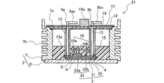
- FIG. 1 is a cross-sectional view of a power semiconductor module according to Embodiment 1 of the present invention.
- FIG. 2 is a cross-sectional view of the power semiconductor module of the second embodiment.
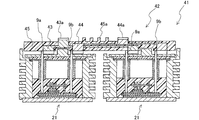
- FIG. 3 is a cross-sectional view of the composite module of the third embodiment.
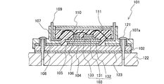
- FIG. 4 is a cross-sectional view of an example of a conventional power semiconductor module.
- the term "electrically and mechanically connected” used in the description of the present application is not limited to the case where the objects are directly connected to each other, and may be solder, sintered metal, etc. This also includes the case where the objects are connected to each other via the conductive bonding material.
- FIG. 1 is a cross-sectional view of a power semiconductor module according to Embodiment 1 of the present invention.
- the power semiconductor module of the present embodiment is a so-called 1-in-1 module, and has a circuit in which switching elements and free-wheeling diodes are connected in antiparallel.
- the power semiconductor module 1 of the present embodiment shown in FIG. 1 includes a housing 2 composed of a base plate 8 and a frame 7, a circuit board 33 which is a part of the insulating substrate 3, and a semiconductor chip 5 as a semiconductor element.
- the metal base plate 8 for heat dissipation has a substantially square planar shape.
- An insulating substrate 3 is bonded onto the base plate 8. As shown in FIG. 1, the insulating substrate 3 is provided on the insulating plate 31, the metal plate 32 provided on one surface of the insulating plate 31, and the other surface of the insulating plate 31, and a predetermined circuit is formed. And a circuit board 33.
- the metal plate 32 of the insulating substrate 3 is bonded to the main surface of the base plate 8 by a bonding material 4 such as solder.
- the insulating plate 31 is made of, for example, an insulating ceramic such as aluminum nitride, silicon nitride, or aluminum oxide, and the metal plate 32 and the circuit plate 33 are made of, for example, copper.
- the circuit board 33 has circuit boards 33a and 33b in which a predetermined circuit is formed in the illustrated example.
- a DCB substrate in which the insulating plate 31 is directly bonded to the metal plate 32 and the circuit board 33 can be used.
- the semiconductor chip 5 is provided with electrodes on the front surface and the back surface.
- the electrode on the back surface is electrically and mechanically connected to the circuit board 33a via a conductive bonding material 6 such as solder.
- the semiconductor chip 5 is, for example, a Schottky barrier diode, a power MOSFET (Metal Oxide Semiconductor Field Effect Transistor), or an IGBT (Insulated Gate Bipolar Transistor).
- the semiconductor chip 5 may be made of a silicon semiconductor or may be made of a SiC semiconductor.
- the electrode on the back surface is a collector electrode
- the electrode on the front surface is an emitter electrode and a gate electrode.
- the semiconductor chip 5 is a power MOSFET made of silicon carbide (SiC), it is possible to perform switching at a high frequency and at a high frequency as compared to a semiconductor chip made of silicon, the power semiconductor module of this embodiment It is optimal as the semiconductor chip 5.
- the semiconductor chip 5 is not limited to the IGBT or the power MOSFET, and may be a combination of one or more semiconductor elements capable of switching operation.
- a frame 7 is provided on the periphery of the base plate 8.
- the frame 7 has a frame shape, and is made of a resin having good insulation, heat resistance, and moldability, such as epoxy resin, PPS (polyphenylene sulfide), PBT (polybutylene terephthalate), or the like.
- the frame 7 may be ceramics.
- the lower end portion of the frame 7 is bonded to the periphery of the main surface of the base plate 8 with an adhesive, and the frame 7 and the base plate 8 constitute a housing 2 of the power semiconductor module 1.
- the insulating substrate 3 and the semiconductor chip 5 are accommodated in the housing 2.
- connection portions 9ac and 9bc One ends of the external terminals 9 a and 9 b are electrically and mechanically connected to the circuit boards 33 a and 33 b in the housing 2.
- the other ends of the external terminals 9a and 9b extend upward and protrude outward beyond a second lid described later to form connection portions 9ac and 9bc.
- the power semiconductor module 1 is provided with a wiring member 10.
- the wiring member 10 is composed of a conductive plate 10a and a conductive post 10b.
- the conductive plate 10 a is provided to face the circuit board 33 of the semiconductor chip 5 and the insulating substrate 3.
- the conductive post 10b has one end electrically and mechanically connected to the second electrode of the semiconductor chip 5 or the circuit board 33 of the insulating substrate 3 and the other end electrically and mechanically connected to the conductive plate 10a.
- the front surface electrode of the semiconductor chip 5 and the circuit board 33 b are electrically connected by the wiring member 10.
- the wiring member is preferably a wiring member 10 formed of the conductive plate 10 a and the conductive post 10 b rather than the bonding wire.
- the second resin 15 injected into the frame 7 is a thermosetting resin
- the thermosetting resin and the other resin are used.
- the bonding wire may be broken due to the difference in linear expansion coefficient with the member.
- the wiring member is formed of the conductive plate 10a and the conductive post 10b, even the thermosetting second resin 15 does not break or the like, and the base plate 8 and the frame 7 are excessively Deformation can be avoided, and both long-term reliability and high insulation performance can be achieved.
- the semiconductor chip 5 is an IGBT
- the wiring member 10 electrically connects the emitter electrode of the front surface electrode to the circuit board 33 b of the insulating substrate 3.
- the wiring member 10 electrically connects the gate electrode of the front surface electrode and the circuit board 33 c (not shown) of the insulating substrate 3.
- the conductive plate 10a and the conductive post 10b are made of, for example, conductive copper.
- the conductive plate 10a and the conductive post 10b can be plated on the surface as needed.
- the outer shape of the conductive post 10 b can be a cylindrical shape, a rectangular solid shape, or the like, but is not particularly limited.
- the bottom surface of the conductive post 10 b is smaller than the front surface electrode of the semiconductor chip 5.
- the number of conductive posts 10b provided for one semiconductor chip 5 is arbitrary, and it is also possible to bond a plurality of conductive posts 10b to one front surface electrode.
- the conductive plate 10a and the conductive post 10b are electrically and mechanically connected by soldering or brazing. Since the power semiconductor module 1 uses the wiring member 10 in which the conductive plate 10a and the conductive post 10b are integrated in advance, the manufacturing process can be simplified.
- the conductive plate 10a is not limited to a copper plate, and may be a circuit board in which a metal layer formed of a conductive metal such as copper or aluminum is formed on at least one surface of the insulating plate. In the case of a circuit board, a configuration having at least two metal layers is preferable.
- One layer is a metal layer for electrically connecting the emitter electrode of the front surface electrode of the semiconductor chip 5 and the circuit board 33 b of the insulating substrate 3.
- Another layer is a metal layer for electrically connecting the gate electrode of the front surface electrode of the semiconductor chip 5 and the circuit board 33 c (not shown) of the insulating substrate 3.
- the second resin 15 is injected into the housing 2 to seal the insulating substrate 3, the semiconductor chip 5, and the wiring member 10, and the exposed surface 15 a of the second resin 15 is formed.
- the second resin 15 is made of a thermosetting resin from the viewpoint of high insulation and resistance to high temperature use.
- an epoxy resin is preferable.
- the second resin 15 covers the wiring member 10 and is injected at a height near the upper end of the wiring member 10.
- the exposed surface 15 a is disposed at a height about 1 mm higher than the upper end of the wiring member 10.
- the exposed surface 15 a may be about 11 mm from the upper surface of the base plate 8.
- the injection amount of the second resin 15 is set to the minimum necessary to cover the wiring member 10 described above.
- the injection amount of the second resin 15 is set to the minimum necessary to cover the wiring member 10 described above.
- the region above the exposed surface 15a in the housing 2 may be a space.
- a space in this region By providing a space in this region and securing the distance between the base plate 8 and the connection portions 9ac and 9bc of the external terminals, the high breakdown voltage characteristics of the power semiconductor module 1 can be secured.
- a sealing material different from the sealing material made of resin for example, a gel-like sealing material can be injected into the region above the second resin 15 to ensure insulation. It is.
- a first lid 12 is provided so as to be locked to the step 7 a provided in the frame 7 and to cover the opening of the housing 2.
- the first lid 12 is made of a resin having good insulation, heat resistance, and moldability, such as epoxy resin, PPS, PBT, or the like. It may be ceramics. Further, a hole is provided in the first lid 12, and the external terminals 9a and 9b are passed through the hole.
- a cover 13 is provided to cover the periphery of the external terminal 9.
- the cover 13 has, for example, a hollow cylindrical shape, and the inner diameter is sized to allow insertion of the external terminals 9a and 9b.
- the cover 13 is made of a resin having good insulation, heat resistance, and moldability, such as epoxy resin, PPS, PBT or the like.
- the upper end of the cover 13 is in contact with the first lid 12, and the lower end does not matter in particular as long as it reaches the second resin 15. In the example shown in FIG. 1, the lower end of the cover 13 reaches the circuit board 33.
- the lower end of the cover 13 is disposed in the vicinity of the exposed surface 15 a of the second resin 15.
- the external terminals 9a and 9b are not exposed to the space and insulation is maintained. Ru. Therefore, the high withstand voltage characteristics of the power semiconductor module 1 can be secured. Moreover, since the combination of the first lid 12 and the cover 13 is not a complicated shape as in the sealing plate described in Patent Document 3, manufacturing is easy and manufacturing cost is low.
- a second lid 14 is provided on the outer side of the housing 2 than the first lid 12. Similar to the first lid 12, the second lid 14 is made of a resin having good insulation, heat resistance, and moldability, such as epoxy resin, PPS, PBT, or the like. Also, the second lid 14 may be a ceramic. A hole is provided in the second lid 14 in the same manner as the first lid 12, and the external terminals 9a and 9b are passed through.
- the first resin 11 is filled between the first lid 12 and the second lid 14. Similarly to the second resin 15, the first resin 11 is preferably an epoxy resin as a thermosetting insulating resin having a high insulating property.
- the high withstand voltage characteristics of the power semiconductor module 1 can be enhanced. Further, the filled first resin 11 is disposed in contact with the external terminals 9a and 9b. The first resin 11 is disposed so as to fill the gap between the external terminals 9a and 9b and the holes through which the external terminals 9a and 9b provided in the first lid 12 and the second lid 14 are inserted. . Thus, the insulation between the inside of the housing 2 and the outside of the power semiconductor module 1 can be secured, and the high breakdown voltage characteristics of the power semiconductor module 1 can be secured. Furthermore, the first resin 11 can also fill the gap that may occur at the contact point between the first lid 12 and the cover 13 and this point is also advantageous for high pressure resistance characteristics.
- the first resin 11 is sufficient if it has a thickness of about 1 mm between the second lid 14 and the first lid 12. Therefore, the second resin 14 and the first lid 12 may be used. The gap between them is about 1 mm. Furthermore, the first resin 11 also functions as an adhesive that fills the gap between the first lid 12 and the second lid 14 and the frame 7 and simultaneously fixes the lids 12 and 14 to the frame 7 doing. As a result, high withstand voltage characteristics can be secured, and there is no need to separately prepare an adhesive for bonding the lid and the frame, so that the manufacturing cost can also be reduced.
- the power semiconductor module 1 of the present embodiment has a high long-term reliability but has a large linear expansion coefficient and a necessary amount of the second resin 15 made of a thermosetting resin having a large thermal stress to cover the wiring member 10 I assume.
- the creepage distance is secured by providing a space between the second resin 15 in the housing 2 and the opening. Also, by covering the external terminals 9a and 9b with the cover 13 in this space, the insulation in the vicinity of the external terminals 9a and 9b is secured. Furthermore, by providing the second lid 14 and the first lid 12 and filling the first resin 11 between them, the insulation at the opening of the housing 2 is enhanced. Therefore, the power semiconductor module 1 of this embodiment can obtain high insulation while maintaining long-term reliability.
- the power semiconductor module 1 is fixed to a cooling member (not shown) with a screw or the like, as in the conventional power semiconductor module. And in order to lengthen the creeping distance between the cooling member and the external terminal which are grounded, and to improve the insulating property, in the present embodiment, the outer surface 7b of the frame 7 is provided with unevenness. These irregularities contribute to the high breakdown voltage characteristics of the power semiconductor module 1 in combination with the above-described configuration. According to this embodiment, a power semiconductor module having extremely high withstand voltage characteristics, for example, a withstand voltage of 13 kV or more can be obtained.
- the pressure resistance characteristic of the power semiconductor module 1 is determined by the height from the cooling member to the connection parts 9ac and 9bc of the external terminals 9a and 9b. Therefore, the distance between the second resin 15 and the first lid 12 may be appropriately adjusted according to the desired pressure resistance characteristics, and the external terminals 9a and 9b having a necessary length may be provided.
- FIG. 2 sectional drawing of the power semiconductor module of Embodiment 2 of this invention is shown.
- the same members as those of the power semiconductor module 1 of the first embodiment shown in FIG. 1 are given the same reference numerals. Therefore, in the description of the power semiconductor module of the second embodiment described below, the overlapping description of the same members as the power semiconductor module 1 of the first embodiment shown in FIG. 1 will be omitted.
- the difference between the power semiconductor module 21 of the second embodiment shown in FIG. 2 and the power semiconductor module 1 of the first embodiment shown in FIG. 1 is that the plurality of external terminals 9a projecting outward from the second lid 14 , 9b (specifically, for example, the P terminal and the N terminal), the projection 14a of the second lid 14 is provided.
- the provision of the projections 14a can enhance the insulation between the external terminals 9a and 9b, and can further enhance the insulation of the power semiconductor module 21.
- FIG. 3 shows a cross-sectional view of a composite module according to Embodiment 3 of the present invention.
- the same members as those of the power semiconductor module 21 of the second embodiment shown in FIG. 2 are denoted by the same reference numerals. Therefore, in the description of the composite module of the third embodiment described below, the redundant description of the same members as the power semiconductor module 21 of the second embodiment will be omitted.
- the composite module 41 illustrated in FIG. 3 includes two power semiconductor modules 21. And the bus-bar unit 42 which electrically connects the same external terminals 9a and 9b which respond
- the bus bar unit 42 has, for example, a bus bar 43 connecting the external terminals 9 a for P terminals and a bus bar 44 connecting the external terminals 9 b for N terminals. And integrally molded. With this configuration, a plurality of power semiconductor modules 21 which are 1 in 1 modules are connected in parallel to configure a 1 in 1 module in which the rated current capacity is increased.
- the connection between the bus bar 43 and the external terminal 9a and the connection between the bus bar 44 and the external terminal 9b are performed by screwing, soldering, laser welding or the like.
- the mold resin 45 is, for example, epoxy resin, PPS, PBT or the like.
- the bus bars 43 and 44 respectively have terminal portions 43a and 44a electrically connected to an external device (not shown). Further, the bus bars 43 and 44 are arranged so as to partially overlap in the vertical direction at an interval of 1 mm or less. Thus, when currents in opposite directions flow through the bus bars 43 and 44, magnetic lines of force due to the currents can be offset to reduce the self-inductance.
- the uneven portion 45a which is integral with the mold resin 45 is provided between the terminal portions 43a and 44a.
- the uneven portion 45a can enhance the insulation between the terminal portions 43a and 44a, and thus can further enhance the insulation of the composite module 41.
- the composite module 41 of the present embodiment connects a plurality of power semiconductor modules in parallel, but can be arranged in a bus bar of the bus bar unit so as to connect in series depending on the application.
- the power semiconductor module and composite module of the present invention were concretely explained using a drawing and an embodiment, the power semiconductor module and composite module of the present invention are not limited to the description of an embodiment and a drawing. Many variations are possible without departing from the spirit of the present invention.
Landscapes
- Cooling Or The Like Of Semiconductors Or Solid State Devices (AREA)
- Structures Or Materials For Encapsulating Or Coating Semiconductor Devices Or Solid State Devices (AREA)
- Physics & Mathematics (AREA)
- Geometry (AREA)
- Inverter Devices (AREA)
- Engineering & Computer Science (AREA)
- Microelectronics & Electronic Packaging (AREA)
Abstract
パワー半導体モジュール1は、筐体2内で半導体素子5のおもて面電極と絶縁基板3の回路板33を電気的に接続する配線部材10を備える。筐体2に設けられた第2の樹脂15は配線部材10を覆いかつ、配線部材10の近傍の高さとする。筐体2内で第2の樹脂15と第1の蓋12の間に、外部端子9a、9bの周囲を覆うカバー13が設けられる。筐体2の開口部で第1の蓋12よりも外方に第2の蓋14が設けられ、第2の蓋14と第1の蓋12との間に第1の樹脂11が充填される。
Description
本発明は、パワー半導体モジュールおよび、このパワー半導体モジュールを組み合わせた複合モジュールに関する。
パワー半導体モジュールは、一般に、半導体素子としての半導体チップが搭載された絶縁基板を備えている。半導体チップと絶縁基板の回路板とは、はんだ等の接合材により、またボンディングワイヤや導電板を通して、電気的に接続されている。絶縁基板及び半導体チップは、筐体に収容される。筐体内の絶縁基板と電気的に接続されている外部端子が筐体よりも外方に延びている。筐体内は、絶縁性を高めるために封止材により封止されている。
従来のパワー半導体モジュールの一例を図4に断面図で示す。
図4に示すパワー半導体モジュール101は、金属製のベース板102を備えている。このベース板102上には、絶縁基板103が接合材104により接合されている。絶縁基板103は、絶縁板131と、絶縁板131の一方の面に設けられた金属板132と、絶縁板131のもう一方の面に設けられ、所定の回路を形成する回路板133とからなる。絶縁基板103は一例ではDCB(Direct Copper Bond)基板である。
図4に示すパワー半導体モジュール101は、金属製のベース板102を備えている。このベース板102上には、絶縁基板103が接合材104により接合されている。絶縁基板103は、絶縁板131と、絶縁板131の一方の面に設けられた金属板132と、絶縁板131のもう一方の面に設けられ、所定の回路を形成する回路板133とからなる。絶縁基板103は一例ではDCB(Direct Copper Bond)基板である。
回路板133に、IGBT(絶縁ゲートバイポーラトランジスタ)などの半導体チップ105が、導電性の接合材106により電気的かつ機械的に接続されている。
ベース板102の周囲に枠体107が設けられ、接合材108により接合されている。これによりパワー半導体モジュール101の筐体が構成されている。枠体107には、枠体107内側から外側へと延びる外部端子109が一体となっている。外部端子109と半導体チップ105のおもて面の電極とが、ボンディングワイヤ110により電気的に接続されている。
ベース板102の周囲に枠体107が設けられ、接合材108により接合されている。これによりパワー半導体モジュール101の筐体が構成されている。枠体107には、枠体107内側から外側へと延びる外部端子109が一体となっている。外部端子109と半導体チップ105のおもて面の電極とが、ボンディングワイヤ110により電気的に接続されている。
枠体107で取り囲まれた空間には半導体チップ105及び絶縁基板103が収容され、この空間内に封止材111が充填されている。これにより、半導体チップ105、絶縁基板103、ベース板102、外部端子109相互間の絶縁性が確保されている。
枠体107には,ねじ孔107aが設けられている。このねじ孔107aにねじ121を通して冷却部材122にねじ結合することにより、パワー半導体モジュール101は冷却部材122に固定される。ベース板102と冷却部材122との間には放熱グリス123が塗布され、これにより半導体チップ105からの熱を、絶縁基板103を通して冷却部材122に良好に伝熱させている。放熱グリス123の代わりに熱伝導シートが用いられることもある。
また、上記のようなパワー半導体モジュールを、バスバーにより複数個並列に接続することも提案されている(特許文献1)。
上記のようなパワー半導体モジュール101の絶縁性能を向上させるため、筐体内に充填される封止材111として、エポキシ樹脂等の熱硬化性樹脂が用いられることがある。一方、封止材111として熱硬化性樹脂を筐体内に多量に用いると、パワー半導体モジュール101の組み立て時の熱履歴及び使用時の外部環境の温度変化等が生じた際に熱応力が生じる。なぜなら、熱硬化性樹脂の線膨張係数が他の部材の線膨張係数と大きく異なるからである。そして、その熱応力により、ボンディングワイヤ110の破断やベース板102や枠体107の変形等が生じるおそれがあった。
ボンディングワイヤ110の破断は、直ちにパワー半導体モジュール101の故障となる。また、ベース板102や枠体107の変形により、冷却部材122との密着度が低下して熱抵抗が増大する。そして、熱抵抗の増大により半導体チップ105の温度の上昇を招き、パワー半導体モジュール101の長期信頼性を低下させるおそれがある。また、熱硬化性樹脂を多量に用いることは、パワー半導体モジュール101のコスト上昇や重量増加にもつながる。
ゲル状の樹脂、例えばシリコーン樹脂を2層に分けて筐体内に注入し、その内1層目の樹脂を補助リード端子に接触しない位置まで注入して硬化させたパワー半導体装置がある(特許文献2)。また、容器内部に充填されたゲル剤の上面と、容器の上蓋に相当する封止板の下面との間に空間が形成され、さらに封止板に設けられた外部端子用の孔をハードレジンで塞いだパワー半導体装置がある(特許文献3)。
しかし、特許文献2や特許文献3に用いられたゲル状のシリコーン樹脂は、耐熱性が熱硬化性樹脂に劣る。また高耐圧用のパワー半導体モジュールにおいて、シリコーン樹脂は絶縁性が必ずしも十分ではなかった。また、特許文献3の封止板の孔をハードレジンで塞ぐ構造は、封止板の形状が複雑であるため、製造コストが上昇する。
しかし、特許文献2や特許文献3に用いられたゲル状のシリコーン樹脂は、耐熱性が熱硬化性樹脂に劣る。また高耐圧用のパワー半導体モジュールにおいて、シリコーン樹脂は絶縁性が必ずしも十分ではなかった。また、特許文献3の封止板の孔をハードレジンで塞ぐ構造は、封止板の形状が複雑であるため、製造コストが上昇する。
本発明は、上記の問題を有利に解決するものであり、高耐圧用のパワー半導体モジュールにおいて、絶縁性が高く、さらにベース板や枠体の変形等を抑制し、長期信頼性の高いものとすることのできるパワー半導体モジュールと、それらを組み合わせた複合モジュールを提供することを目的とする。
本発明の一様態のパワー半導体モジュールは、開口部を有する筐体と、前記筐体の内部に収容された回路板と、おもて面に電極を有し、裏面が前記回路板に固定された半導体素子と、前記半導体素子の電極と前記回路板との間を電気的に接続する配線部材と、前記筐体の開口部に固定された第1の蓋と、前記筐体の開口部に固定され、前記第1の蓋よりも外方に設けられた第2の蓋と、前記第1の蓋と前記第2の蓋との間に配置された第1の樹脂と、前記配線部材を覆い、露出面を有し、前記露出面が前記第1の蓋よりも前記配線部材に近い第2の樹脂と、一端が前記回路板に電気的かつ機械的に接続され、他端が前記第2の蓋よりも外方に突出した外部端子と、前記外部端子を覆い、前記第2の樹脂の露出面と前記第1の蓋との間に配置されたカバーとを備えている。
また本発明の別の様態の複合モジュールは、上記のパワー半導体モジュールを複数個備え、各パワー半導体モジュールの前記外部端子同士を電気的に接続するバスバーユニットを備えている。
本発明のパワー半導体モジュール及び複合モジュールによれば、高耐圧用のパワー半導体モジュールにおいて、絶縁性が高く、さらにベース板やケースの変形等を抑制し、長期信頼性の高いものとすることができる。
以下、本発明のパワー半導体モジュールの実施形態について、図面を参照しつつ具体的に説明する。なお、本出願の記載に用いられている「電気的かつ機械的に接続されている」という用語は、対象物同士が直接接合により接続されている場合に限られず、ハンダや金属焼結材などの導電性の接合材を介して対象物同士が接続されている場合も含むものとする。
(実施形態1)
図1は、本発明の実施形態1のパワー半導体モジュールの断面図である。本実施形態のパワー半導体モジュールは、いわゆる1in1モジュールと呼称されるものであり、スイッチング素子と還流ダイオードが逆並列に接続された回路を有している。
図1に示した本実施形態のパワー半導体モジュール1は、ベース板8と枠体7からなる筐体2と、絶縁基板3の一部である回路板33と、半導体素子としての半導体チップ5と、配線部材10と、第1の蓋12と、第2の蓋14と、第1の樹脂11と、第2の樹脂15と、外部端子9(9a、9b)と、カバー13を備えている。
放熱用の金属製のベース板8は、略四角形の平面形状を有している。このベース板8上には、絶縁基板3が接合されている。絶縁基板3は図1で示すとおり、絶縁板31と、絶縁板31の一方の面に設けられた金属板32と、絶縁板31のもう一方の面に設けられ、所定の回路が形成された回路板33とで構成されている。絶縁基板3の金属板32は、ベース板8の主面と、はんだなどの接合材4により接合されている。絶縁板31は例えば窒化アルミニウムや窒化珪素、酸化アルミニウム等の絶縁性セラミックスよりなり、金属板32、回路板33は、例えば銅よりなる。そして回路板33は、図示した例では所定の回路が形成された回路板33a、33bを有している。絶縁基板3は、これらの絶縁板31と金属板32、回路板33とを直接接合したDCB基板等を用いることができる。
図1は、本発明の実施形態1のパワー半導体モジュールの断面図である。本実施形態のパワー半導体モジュールは、いわゆる1in1モジュールと呼称されるものであり、スイッチング素子と還流ダイオードが逆並列に接続された回路を有している。
図1に示した本実施形態のパワー半導体モジュール1は、ベース板8と枠体7からなる筐体2と、絶縁基板3の一部である回路板33と、半導体素子としての半導体チップ5と、配線部材10と、第1の蓋12と、第2の蓋14と、第1の樹脂11と、第2の樹脂15と、外部端子9(9a、9b)と、カバー13を備えている。
放熱用の金属製のベース板8は、略四角形の平面形状を有している。このベース板8上には、絶縁基板3が接合されている。絶縁基板3は図1で示すとおり、絶縁板31と、絶縁板31の一方の面に設けられた金属板32と、絶縁板31のもう一方の面に設けられ、所定の回路が形成された回路板33とで構成されている。絶縁基板3の金属板32は、ベース板8の主面と、はんだなどの接合材4により接合されている。絶縁板31は例えば窒化アルミニウムや窒化珪素、酸化アルミニウム等の絶縁性セラミックスよりなり、金属板32、回路板33は、例えば銅よりなる。そして回路板33は、図示した例では所定の回路が形成された回路板33a、33bを有している。絶縁基板3は、これらの絶縁板31と金属板32、回路板33とを直接接合したDCB基板等を用いることができる。
半導体チップ5は、おもて面および裏面にそれぞれ電極が設けられている。そして、裏面の電極がはんだなどの導電性の接合材6を介して、回路板33aに電気的かつ機械的に接続されている。半導体チップ5は、具体的には、例えばショットキーバリアダイオードやパワーMOSFET(Metal Oxide Semiconductor Field Effect Transistor)やIGBT(Insulated Gate Bipolar Transistor)である。半導体チップ5はシリコン半導体からなるものでもよいし、SiC半導体からなるものでもよい。半導体チップ5がIGBTの場合では、裏面の電極はコレクタ電極であり、おもて面の電極はエミッタ電極及びゲート電極である。半導体チップ5が炭化ケイ素(SiC)からなるパワーMOSFETである場合は、シリコンからなる半導体チップに比べて高耐圧で、かつ高周波でのスイッチングが可能であるために、本実施形態のパワー半導体モジュールの半導体チップ5として最適である。もっとも、半導体チップ5は、IGBTやパワーMOSFETに限定されず、スイッチングの動作が可能な半導体素子の一個又は複数個の組み合わせであればよい。
ベース板8の周縁に枠体7が設けられている。枠体7は枠形状を有し、絶縁性、耐熱性、成形性のよい樹脂、例えばエポキシ樹脂やPPS(Polyphenylene Sulfide)、PBT(Polybutylene terephthalate)等からなる。また、枠体7はセラミックスでも構わない。枠体7の下端部は、ベース板8の主面の周縁に接着剤により接合され、枠体7とベース板8によりパワー半導体モジュール1の筐体2が構成されている。筐体2内には絶縁基板3や半導体チップ5が収容される。筐体2内の回路板33a、33bに、外部端子9a、9bの一端が電気的かつ機械的に接続されている。外部端子9a、9bの他端は、上方に延び、後述する第2の蓋よりも外方に突出し、接続部9ac、9bcを構成している。
パワー半導体モジュール1には、配線部材10が設けられている。配線部材10は、導電板10aと、導電ポスト10bにより構成されている。導電板10aは、半導体チップ5及び絶縁基板3の回路板33に対向して設けられている。そして、導電ポスト10bは、一端が半導体チップ5の第2電極又は絶縁基板3の回路板33に電気的かつ機械的に接続され、他端が導電板10aと電気的かつ機械的に接続されている。
配線部材10により、例えば半導体チップ5のおもて面電極と、回路板33bとが電気的に接続される。本実施形態において配線部材はボンディングワイヤよりも、導電板10aと導電ポスト10bで構成された配線部材10が好ましい。後述するように本実施形態においては、枠体7内に注入される第2の樹脂15が熱硬化性樹脂であるため、配線部材がボンディングワイヤである場合には、熱硬化性樹脂と他の部材との線膨張係数の相違によってボンディングワイヤが破断するおそれがあった。これに対し配線部材が導電板10aと導電ポスト10bで構成される場合には、熱硬化性の第2の樹脂15であっても破断等が生じず、またベース板8や枠体7の過度な変形も回避することができ、長期信頼性と高絶縁性能との両立が可能となる。配線部材10は、例えば半導体チップ5がIGBTである場合には、おもて面電極のうちのエミッタ電極と、絶縁基板3の回路板33bを電気的に接続している。また、配線部材10は、おもて面電極のうちのゲート電極と、絶縁基板3の回路板33c(図示せず)を電気的に接続している。
配線部材10により、例えば半導体チップ5のおもて面電極と、回路板33bとが電気的に接続される。本実施形態において配線部材はボンディングワイヤよりも、導電板10aと導電ポスト10bで構成された配線部材10が好ましい。後述するように本実施形態においては、枠体7内に注入される第2の樹脂15が熱硬化性樹脂であるため、配線部材がボンディングワイヤである場合には、熱硬化性樹脂と他の部材との線膨張係数の相違によってボンディングワイヤが破断するおそれがあった。これに対し配線部材が導電板10aと導電ポスト10bで構成される場合には、熱硬化性の第2の樹脂15であっても破断等が生じず、またベース板8や枠体7の過度な変形も回避することができ、長期信頼性と高絶縁性能との両立が可能となる。配線部材10は、例えば半導体チップ5がIGBTである場合には、おもて面電極のうちのエミッタ電極と、絶縁基板3の回路板33bを電気的に接続している。また、配線部材10は、おもて面電極のうちのゲート電極と、絶縁基板3の回路板33c(図示せず)を電気的に接続している。
導電板10aや導電ポスト10bは、例えば導電性のよい銅よりなる。また、導電板10aや導電ポスト10bは、必要に応じてめっきを表面に施すことができる。導電ポスト10bの外形は、円柱形状、直方体形状等の形状とすることができるが特に限定されない。導電ポスト10bの底面は、半導体チップ5のおもて面電極より小さい大きさである。更に、一つの半導体チップ5に対する導電ポスト10bの設置数は任意であり、一つのおもて面電極に複数個の導電ポスト10bを接合することも可能である。
導電板10aと導電ポスト10bとは、はんだやロウ付けにより電気的かつ機械的に接続されている。パワー半導体モジュール1は、導電板10aと導電ポスト10bとをあらかじめ一体化した配線部材10を用いているので、その製造工程を簡素化することができる。
また、導電板10aは銅板に限られず、絶縁板の少なくとも一方の表面に、銅やアルミニウム等の導電性金属により形成された金属層が形成された回路基板であってもよい。回路基板である場合は、少なくとも2層の金属層を有する構成が好ましい。一層は、半導体チップ5のおもて面電極のうちのエミッタ電極と、絶縁基板3の回路板33bを電気的に接続するための金属層である。もう一層は、半導体チップ5のおもて面電極のうちのゲート電極と、絶縁基板3の回路板33c(図示せず)を電気的に接続するための金属層である。
筐体2内に第2の樹脂15が注入され、絶縁基板3、半導体チップ5、配線部材10が封止され、第2の樹脂15の露出面15aが形成される。第2の樹脂15は、絶縁性が高く、更に高温使用に耐えられるという観点から熱硬化性の樹脂とし、例えばエポキシ樹脂が好ましい。第2の樹脂15は、配線部材10を覆い、かつ配線部材10の上端の近傍の高さで注入される。具体的には、配線部材10の上端より1mm程度高い高さに、露出面15aが配置される。例えば、ベース板8の上面から配線部材10の上端までの高さを10mm程度にした場合、露出面15aはベース板8の上面から11mm程度の高さにすると良い。第2の樹脂15の注入量が多いほど、筐体2内で第2の樹脂15による熱応力が発生し易く、パワー半導体モジュールの長期信頼性が低下する。また、コストや軽量化の観点からも不利である。よって本実施形態では、第2の樹脂15の注入量を、上述した配線部材10を覆うだけの必要最小限とする。これにより、パワー半導体モジュール1の変形を抑制するとともに、パワー半導体モジュール1のコストアップ、重量アップを回避することが可能となる。また、前述のように配線部材を導電板10aと導電ポスト10bで構成することにより、従来例のボンディングワイヤによる配線に比べて、配線部材の上端の高さを正確に制御することができる。このため、第2の樹脂15の注入量を上記のように必要かつ最小限に制御することができるため、有効である。
筐体2内における露出面15aよりも上側の領域は、空間とすればよい。この領域に空間を設け、ベース板8と外部端子の接続部9ac、9bcとの距離を確保することによって、パワー半導体モジュール1の高耐圧特性が確保できる。また別の例として,第2の樹脂15より上側の領域に、樹脂よりなる封止材とは別の封止材、例えばゲル状の封止材を注入して絶縁性を確保することも可能である。
枠体7に設けられた段差部7aに係止され、筐体2の開口部を覆うように、第1の蓋12が設けられる。第1の蓋12は、絶縁性、耐熱性、成形性のよい樹脂、例えばエポキシ樹脂やPPS、PBTなどからなる。セラミックスでも構わない。また第1の蓋12には孔が設けられていて、その孔に外部端子9a、9bが通される。
第1の蓋12と、第2の樹脂15の露出面15aとの間の空間において、外部端子9の周囲を覆って、カバー13が設けられている。カバー13は、一例では中空の円筒形状であって、内径が外部端子9a、9bを挿入可能な大きさになっている。カバー13は、絶縁性、耐熱性、成形性のよい樹脂、例えばエポキシ樹脂やPPS、PBTなどからなる。カバー13の上端は第1の蓋12に当接し、下端は第2の樹脂15内に達していれば特に位置を問わない。なお図1に示した例では、カバー13の下端は回路板33まで達している。また別の例として図3に示した例では、カバー13の下端が第2の樹脂15の露出面15aの近傍に配置されている。
第1の蓋12と第2の樹脂15との間の空間で、外部端子9a、9bをカバー13で覆うことにより、外部端子9a、9bは空間に露出することがなくなって絶縁性が維持される。そのため、パワー半導体モジュール1の高耐圧特性を確保することができる。また、第1の蓋12とカバー13との組み合わせは、特許文献3に記載された封止板のような複雑形状ではないため製造が容易であり、製造コストが安価に済む。
第1の蓋12よりも筐体2の外方に、第2の蓋14が設けられる。第2の蓋14は、第1の蓋12と同様に、絶縁性、耐熱性、成形性のよい樹脂、例えばエポキシ樹脂やPPS、PBTなどからなる。また、第2の蓋14はセラミックスでも構わない。第2の蓋14にも第1の蓋12と同様に孔が設けられていて、外部端子9a、9bが通される。
第1の蓋12と第2の蓋14との間には、第1の樹脂11が充填される。第1の樹脂11は、第2の樹脂15と同様に、絶縁性が高い熱硬化性の絶縁性樹脂として、エポキシ樹脂が好ましい。
第1の蓋12と第2の蓋14との間に第1の樹脂11が充填されたことにより、パワー半導体モジュール1の高耐圧特性を高めることができる。また、充填された第1の樹脂11は外部端子9a、9bに接するように配置される。そして、第1の樹脂11は、第1の蓋12及び第2の蓋14に設けられた外部端子9a、9bを挿通する孔と、外部端子9a、9bとの隙間を埋めるように配置される。これにより、筐体2の内部とパワー半導体モジュール1の外部との絶縁が確保でき、パワー半導体モジュール1の高耐圧特性を確保することができる。
さらに第1の樹脂11は、第1の蓋12とカバー13との当接箇所に生じ得る隙間を埋めることも可能であり、この点でも、高耐圧特性に有利である。第1の樹脂11は第2の蓋14と第1の蓋12との間で、1mm程度の厚さを有していれば十分であるため、第2の蓋14と第1の蓋12との間の間隙は、1mm程度とする。
またさらに第1の樹脂11は、第1の蓋12および第2の蓋14と、枠体7との間の隙間を埋め、同時に蓋12、14を枠体7に固定する接着材としても機能している。これにより、高耐圧特性を確保できるとともに、蓋と枠体を接着する接着材を別途準備する必要がなくなるため、製造コストも低減可能である。
さらに第1の樹脂11は、第1の蓋12とカバー13との当接箇所に生じ得る隙間を埋めることも可能であり、この点でも、高耐圧特性に有利である。第1の樹脂11は第2の蓋14と第1の蓋12との間で、1mm程度の厚さを有していれば十分であるため、第2の蓋14と第1の蓋12との間の間隙は、1mm程度とする。
またさらに第1の樹脂11は、第1の蓋12および第2の蓋14と、枠体7との間の隙間を埋め、同時に蓋12、14を枠体7に固定する接着材としても機能している。これにより、高耐圧特性を確保できるとともに、蓋と枠体を接着する接着材を別途準備する必要がなくなるため、製造コストも低減可能である。
本実施形態のパワー半導体モジュール1は、長期信頼性は高い一方、線膨張係数が大きく、熱応力の大きい熱硬化性樹脂からなる第2の樹脂15を、配線部材10を覆う必要最小限の量とする。そして、筐体2内の第2の樹脂15と開口部との間に空間を設けることにより、沿面距離を確保している。また、この空間内で外部端子9a、9bをカバー13で覆うことにより外部端子9a、9b近傍の絶縁性を確保している。更に、第2の蓋14と第1の蓋12とを設け、これらの間に第1の樹脂11を充填することより、筐体2の開口部での絶縁性を高めている。したがって、本実施形態のパワー半導体モジュール1は、長期信頼性を維持しつつ高い絶縁性を得ることができる。
パワー半導体モジュール1は、従来のパワー半導体モジュールと同様に、冷却部材(図示せず)にねじなどで固定される。そして接地されている冷却部材と外部端子と間の沿面距離を長くして絶縁性を高めるために、本実施形態では枠体7の外面7bには凹凸が設けられている。これらの凹凸が、上述した構成と相まって、パワー半導体モジュール1の高耐圧特性に寄与している。本実施形態により、例えば耐圧13kV以上という、極めて高い耐圧特性を具備するパワー半導体モジュールが得られる。なお、パワー半導体モジュール1の耐圧特性は、冷却部材から外部端子9a、9bの接続部9ac、9bcまでの高さ、で決まる。そのため、所望の耐圧特性に合わせて、第2の樹脂15と第1の蓋12との間隔を適宜調整し、必要な長さの外部端子9a、9bを設ければよい。
(実施形態2)
図2に、本発明の実施形態2のパワー半導体モジュールの断面図を示す。図2においては、図1に示した実施形態1のパワー半導体モジュール1と同一の部材について同一の符号を付した。したがって、以下に述べる実施形態2のパワー半導体モジュールの説明では、図1に示した実施形態1のパワー半導体モジュール1と同一の部材についての重複する説明は省略する。
図2に、本発明の実施形態2のパワー半導体モジュールの断面図を示す。図2においては、図1に示した実施形態1のパワー半導体モジュール1と同一の部材について同一の符号を付した。したがって、以下に述べる実施形態2のパワー半導体モジュールの説明では、図1に示した実施形態1のパワー半導体モジュール1と同一の部材についての重複する説明は省略する。
図2に示した実施形態2のパワー半導体モジュール21の、図1に示した実施形態1のパワー半導体モジュール1との相違点は、第2の蓋14から外方に突出する複数の外部端子9a、9b(具体的には例えばP端子とN端子)の間に、第2の蓋14の突起14aを設けた点である。突起14aが設けられたことにより、外部端子9a、9b間の絶縁性を高めることができ、ひいてはパワー半導体モジュール21の絶縁性を、より高めることができる。
(実施形態3)
図3に、本発明の実施形態3の複合モジュールの断面図を示す。図3においては、図2に示した実施形態2のパワー半導体モジュール21と同一の部材について同一の符号を付した。したがって、以下に述べる実施形態3の複合モジュールの説明では、実施形態2のパワー半導体モジュール21と同一の部材についての重複する説明は省略する。
図3に、本発明の実施形態3の複合モジュールの断面図を示す。図3においては、図2に示した実施形態2のパワー半導体モジュール21と同一の部材について同一の符号を付した。したがって、以下に述べる実施形態3の複合モジュールの説明では、実施形態2のパワー半導体モジュール21と同一の部材についての重複する説明は省略する。
図3に示した複合モジュール41は、2個のパワー半導体モジュール21を備えている。そして、2個のパワー半導体モジュール21において対応する同一の外部端子9a、9b同士を電気的に接続する、バスバーユニット42を備えている。バスバーユニット42は、例えばP端子用の外部端子9a同士を接続するバスバー43と、N端子用の外部端子9b同士を接続するバスバー44とを有し、バスバー43、44を絶縁性のモールド樹脂45で一体的に成形してなるものである。この構成により、1in1モジュールであるパワー半導体モジュール21を複数並列に接続し、定格の電流容量を増加させた1in1モジュールが構成される。バスバー43と外部端子9aとの接続やバスバー44と外部端子9bとの接続は、ねじ止め、はんだ、レーザ溶接等によって行われる。またモールド樹脂45は、例えばエポキシ樹脂、PPS、PBT等である。バスバー43、44は、それぞれ外部装置(図示せず)と電気的に接続する端子部43a、44aを有している。またバスバー43、44は、1mm以下の間隔を空け、上下方向に部分的に重なり合うように配置されている。これにより、バスバー43、44に互いに逆向きの電流が流れるとき、その電流による磁力線を相殺させ、自己インダクタンスを低減させることができる。
また、バスバーユニット42には、端子部43aと44aとの間に、モールド樹脂45と一体である凹凸部45aが設けられている。凹凸部45aにより端子部43aと44a間の絶縁性を高めることができ、ひいては複合モジュール41の絶縁性を、より高めることができる。
本実施形態の複合モジュール41は、複数のパワー半導体モジュールを並列に接続しているが、用途に応じ、直列に接続するようにバスバーユニットのバスバー配置とすることができる。
以上、本発明のパワー半導体モジュール及び複合モジュールを図面及び実施形態を用いて具体的に説明したが、本発明のパワー半導体モジュール及び複合モジュールは、実施形態及び図面の記載に限定されるものではなく、本発明の趣旨を逸脱しない範囲で幾多の変形が可能である。
1、21 パワー半導体モジュール
2 筐体
3 絶縁基板
31 絶縁板
32 金属板
33 回路板
4、6 接合材
5 半導体チップ(半導体素子)
7 枠体
8 ベース板
9a、9b 外部端子
9ac、9bc 接続部
10 配線部材
10a 導電板
10b 導電ポスト
11 第1の樹脂
12 第1の蓋
13 カバー
14 第2の蓋
15 第2の樹脂
15a 露出面
41 複合モジュール
42 バスバーユニット
43、44 バスバー
45 モールド樹脂
2 筐体
3 絶縁基板
31 絶縁板
32 金属板
33 回路板
4、6 接合材
5 半導体チップ(半導体素子)
7 枠体
8 ベース板
9a、9b 外部端子
9ac、9bc 接続部
10 配線部材
10a 導電板
10b 導電ポスト
11 第1の樹脂
12 第1の蓋
13 カバー
14 第2の蓋
15 第2の樹脂
15a 露出面
41 複合モジュール
42 バスバーユニット
43、44 バスバー
45 モールド樹脂
Claims (14)
- 開口部を有する筐体と、
前記筐体の内部に収容された回路板と、
おもて面に電極を有し、裏面が前記回路板に固定された半導体素子と、
前記半導体素子の電極と前記回路板との間を電気的に接続する配線部材と、
前記筐体の開口部に固定された第1の蓋と、
前記筐体の開口部に固定され、前記第1の蓋よりも外方に設けられた第2の蓋と、
前記第1の蓋と前記第2の蓋との間に配置された第1の樹脂と、
前記配線部材を覆い、露出面を有し、前記露出面が前記第1の蓋よりも前記配線部材に近い第2の樹脂と、
一端が前記回路板に電気的かつ機械的に接続され、他端が前記第2の蓋よりも外方に突出した外部端子と、
前記外部端子を覆い、前記第2の樹脂の露出面と前記第1の蓋との間に配置されたカバーと、
を備えるパワー半導体モジュール。 - 前記第1の蓋と前記第2の蓋の間において、前記外部端子は前記第1の樹脂で封止されている請求項1記載のパワー半導体モジュール。
- 前記配線部材が、前記半導体素子及び前記回路板に対向して設けられた導電板と、
一端が前記半導体素子の第2電極又は前記回路板に電気的かつ機械的に接続され、他端が前記導電板と電気的かつ機械的に接続される導電ポストとを有する請求項1記載のパワー半導体モジュール。 - 前記筐体の外部の側面に凹凸を有する請求項1記載のパワー半導体モジュール。
- 前記第2の蓋が、外部に突出する複数の前記外部端子の間に突起を有する請求項1記載のパワー半導体モジュール。
- 前記第1の樹脂および前記第2の樹脂が、熱硬化性樹脂である請求項1記載のパワー半導体モジュール。
- 前記カバーが、前記筐体の内部の側面と離れて設けられた請求項1記載のパワー半導体モジュール。
- 前記半導体素子が裏面に他の電極を有する縦型半導体素子であり、前記他の電極と前記回路板が電気的かつ機械的に接続されている請求項1記載のパワー半導体モジュール。
- 前記筐体が、枠体とベース板からなる請求項1記載のパワー半導体モジュール。
- 前記回路板が絶縁基板の一部であり、前記絶縁基板は前記ベース板に固定されている請求項9記載のパワー半導体モジュール。
- 前記配線部材と、前記露出面が約1mm離れている請求項1記載のパワー半導体モジュール。
- 請求項1記載のパワー半導体モジュールを複数個備え、各パワー半導体モジュールの前記外部端子同士を電気的に接続するバスバーユニットを備える複合モジュール。
- 前記バスバーユニットは、複数のバスバーを間隔を空けて部分的に重ね合わせてなる請求項12記載の複合モジュール。
- 前記バスバーユニットにおける複数のバスバーの間隔が1mm以下である請求項13記載の複合モジュール。
Priority Applications (3)
| Application Number | Priority Date | Filing Date | Title |
|---|---|---|---|
| JP2016519154A JP6233507B2 (ja) | 2014-05-15 | 2015-04-01 | パワー半導体モジュールおよび複合モジュール |
| CN201580002601.9A CN105765716B (zh) | 2014-05-15 | 2015-04-01 | 功率半导体模块和复合模块 |
| US15/150,938 US9761567B2 (en) | 2014-05-15 | 2016-05-10 | Power semiconductor module and composite module |
Applications Claiming Priority (2)
| Application Number | Priority Date | Filing Date | Title |
|---|---|---|---|
| JP2014-101423 | 2014-05-15 | ||
| JP2014101423 | 2014-05-15 |
Related Child Applications (1)
| Application Number | Title | Priority Date | Filing Date |
|---|---|---|---|
| US15/150,938 Continuation US9761567B2 (en) | 2014-05-15 | 2016-05-10 | Power semiconductor module and composite module |
Publications (1)
| Publication Number | Publication Date |
|---|---|
| WO2015174158A1 true WO2015174158A1 (ja) | 2015-11-19 |
Family
ID=54479702
Family Applications (1)
| Application Number | Title | Priority Date | Filing Date |
|---|---|---|---|
| PCT/JP2015/060340 Ceased WO2015174158A1 (ja) | 2014-05-15 | 2015-04-01 | パワー半導体モジュールおよび複合モジュール |
Country Status (4)
| Country | Link |
|---|---|
| US (1) | US9761567B2 (ja) |
| JP (1) | JP6233507B2 (ja) |
| CN (1) | CN105765716B (ja) |
| WO (1) | WO2015174158A1 (ja) |
Cited By (5)
| Publication number | Priority date | Publication date | Assignee | Title |
|---|---|---|---|---|
| JP2020526930A (ja) * | 2017-07-12 | 2020-08-31 | アー・ベー・ベー・パワー・グリッズ・スウィツァーランド・アクチェンゲゼルシャフトAbb Power Grids Switzerland Ag | パワー半導体モジュール |
| CN111900133A (zh) * | 2019-05-06 | 2020-11-06 | 英飞凌科技股份有限公司 | 功率半导体模块装置 |
| JP2023045654A (ja) * | 2021-09-22 | 2023-04-03 | 株式会社東芝 | 半導体装置 |
| DE102016213914B4 (de) | 2015-09-15 | 2024-05-08 | Fuji Electric Co., Ltd. | Halbleitervorrichtung |
| JP2025094152A (ja) * | 2019-01-10 | 2025-06-24 | ウルフスピード インコーポレイテッド | 低インダクタンスおよび高速スイッチングを有する、パワーデバイスを並列化するための高電力多層モジュール |
Families Citing this family (14)
| Publication number | Priority date | Publication date | Assignee | Title |
|---|---|---|---|---|
| EP4064328B1 (en) * | 2021-03-25 | 2025-03-05 | Infineon Technologies AG | Housing, semiconductor module and methods for producing the same |
| JP6759784B2 (ja) * | 2016-07-12 | 2020-09-23 | 三菱電機株式会社 | 半導体モジュール |
| JP6786416B2 (ja) * | 2017-02-20 | 2020-11-18 | 株式会社東芝 | 半導体装置 |
| JP6769541B2 (ja) * | 2017-02-23 | 2020-10-14 | 三菱電機株式会社 | 半導体装置 |
| US10283447B1 (en) * | 2017-10-26 | 2019-05-07 | Infineon Technologies Ag | Power semiconductor module with partially coated power terminals and method of manufacturing thereof |
| US10756162B2 (en) | 2018-08-31 | 2020-08-25 | Taiwan Semiconductor Manufacturing Co., Ltd. | Structure and formation method of semiconductor device with magnetic element |
| FR3089057B1 (fr) * | 2018-11-28 | 2021-09-10 | Inst Supergrid | Système incluant un module électrique de puissance et une gaine contre les arcs électriques |
| EP3736855A1 (en) | 2019-05-06 | 2020-11-11 | Infineon Technologies AG | Power semiconductor module arrangement and method for producing the same |
| EP3736854A1 (en) | 2019-05-06 | 2020-11-11 | Infineon Technologies AG | Power semiconductor module arrangement |
| WO2021019802A1 (ja) * | 2019-07-30 | 2021-02-04 | 株式会社三社電機製作所 | 半導体モジュール |
| CN111128022B (zh) * | 2019-12-24 | 2021-04-23 | 云谷(固安)科技有限公司 | 一种显示面板及其制备方法、显示装置 |
| US12514127B2 (en) | 2021-01-25 | 2025-12-30 | Seiko Epson Corporation | Electronic device and method for manufacturing electronic device |
| CN113594103A (zh) * | 2021-08-06 | 2021-11-02 | 广东汇芯半导体有限公司 | 半导体电路 |
| CN117766470B (zh) * | 2024-02-20 | 2024-05-14 | 北京怀柔实验室 | 半导体器件的封装结构和封装方法 |
Citations (6)
| Publication number | Priority date | Publication date | Assignee | Title |
|---|---|---|---|---|
| JPS58175650U (ja) * | 1982-05-19 | 1983-11-24 | 日本電気株式会社 | 樹脂封止型半導体装置 |
| JPS63132448U (ja) * | 1987-02-20 | 1988-08-30 | ||
| JPH113995A (ja) * | 1997-06-12 | 1999-01-06 | Toshiba Corp | 半導体装置 |
| JP2003068979A (ja) * | 2001-08-28 | 2003-03-07 | Hitachi Ltd | 半導体装置 |
| US20090213553A1 (en) * | 2008-02-27 | 2009-08-27 | Infineon Technologies Ag | Power Module |
| JP2012119618A (ja) * | 2010-12-03 | 2012-06-21 | Fuji Electric Co Ltd | パワー半導体モジュール |
Family Cites Families (26)
| Publication number | Priority date | Publication date | Assignee | Title |
|---|---|---|---|---|
| US4127840A (en) * | 1977-02-22 | 1978-11-28 | Conrac Corporation | Solid state force transducer |
| EP0346061A3 (en) * | 1988-06-08 | 1991-04-03 | Fujitsu Limited | Integrated circuit device having an improved package structure |
| DE3915707A1 (de) * | 1989-05-13 | 1990-11-22 | Asea Brown Boveri | Kunststoffgehaeuse und leistungshalbleitermodul mit diesem gehaeuse |
| JPH04196580A (ja) * | 1990-11-28 | 1992-07-16 | Mitsubishi Electric Corp | 半導体装置 |
| US5268533A (en) * | 1991-05-03 | 1993-12-07 | Hughes Aircraft Company | Pre-stressed laminated lid for electronic circuit package |
| US5257547A (en) * | 1991-11-26 | 1993-11-02 | Honeywell Inc. | Amplified pressure transducer |
| JPH10270608A (ja) | 1997-03-28 | 1998-10-09 | Hitachi Ltd | 樹脂封止型パワー半導体装置 |
| DE29900370U1 (de) * | 1999-01-12 | 1999-04-08 | eupec Europäische Gesellschaft für Leistungshalbleiter mbH & Co. KG, 59581 Warstein | Leistungshalbleitermodul mit Deckel |
| US7166910B2 (en) * | 2000-11-28 | 2007-01-23 | Knowles Electronics Llc | Miniature silicon condenser microphone |
| NZ531008A (en) * | 2001-08-10 | 2006-08-31 | Black & Decker Inc | Electrically isolated module |
| JP3813098B2 (ja) * | 2002-02-14 | 2006-08-23 | 三菱電機株式会社 | 電力用半導体モジュール |
| US6781231B2 (en) * | 2002-09-10 | 2004-08-24 | Knowles Electronics Llc | Microelectromechanical system package with environmental and interference shield |
| US7692292B2 (en) * | 2003-12-05 | 2010-04-06 | Panasonic Corporation | Packaged electronic element and method of producing electronic element package |
| US7608789B2 (en) * | 2004-08-12 | 2009-10-27 | Epcos Ag | Component arrangement provided with a carrier substrate |
| JP4338620B2 (ja) * | 2004-11-01 | 2009-10-07 | 三菱電機株式会社 | 半導体装置及びその製造方法 |
| US7202552B2 (en) * | 2005-07-15 | 2007-04-10 | Silicon Matrix Pte. Ltd. | MEMS package using flexible substrates, and method thereof |
| US20070075417A1 (en) * | 2005-10-05 | 2007-04-05 | Samsung Electro-Mechanics Co., Ltd. | MEMS module package using sealing cap having heat releasing capability and manufacturing method thereof |
| US8154114B2 (en) * | 2007-08-06 | 2012-04-10 | Infineon Technologies Ag | Power semiconductor module |
| JP4553043B2 (ja) * | 2008-09-12 | 2010-09-29 | 株式会社村田製作所 | 音響的トランスデューサユニット |
| US8325951B2 (en) * | 2009-01-20 | 2012-12-04 | General Mems Corporation | Miniature MEMS condenser microphone packages and fabrication method thereof |
| JP2011198866A (ja) * | 2010-03-18 | 2011-10-06 | Renesas Electronics Corp | 半導体装置およびその製造方法 |
| JP2012105382A (ja) | 2010-11-08 | 2012-05-31 | Hitachi Ltd | 半導体装置 |
| JP2012138531A (ja) * | 2010-12-28 | 2012-07-19 | Sansha Electric Mfg Co Ltd | 半導体パワーモジュール |
| JP2012238684A (ja) * | 2011-05-11 | 2012-12-06 | Mitsubishi Electric Corp | 電力用半導体装置 |
| WO2013076830A1 (ja) * | 2011-11-22 | 2013-05-30 | 富士通株式会社 | 電子部品およびその製造方法 |
| KR20140057979A (ko) * | 2012-11-05 | 2014-05-14 | 삼성전자주식회사 | 반도체 패키지 및 반도체 패키지의 제조 방법 |
-
2015
- 2015-04-01 JP JP2016519154A patent/JP6233507B2/ja not_active Expired - Fee Related
- 2015-04-01 WO PCT/JP2015/060340 patent/WO2015174158A1/ja not_active Ceased
- 2015-04-01 CN CN201580002601.9A patent/CN105765716B/zh not_active Expired - Fee Related
-
2016
- 2016-05-10 US US15/150,938 patent/US9761567B2/en not_active Expired - Fee Related
Patent Citations (6)
| Publication number | Priority date | Publication date | Assignee | Title |
|---|---|---|---|---|
| JPS58175650U (ja) * | 1982-05-19 | 1983-11-24 | 日本電気株式会社 | 樹脂封止型半導体装置 |
| JPS63132448U (ja) * | 1987-02-20 | 1988-08-30 | ||
| JPH113995A (ja) * | 1997-06-12 | 1999-01-06 | Toshiba Corp | 半導体装置 |
| JP2003068979A (ja) * | 2001-08-28 | 2003-03-07 | Hitachi Ltd | 半導体装置 |
| US20090213553A1 (en) * | 2008-02-27 | 2009-08-27 | Infineon Technologies Ag | Power Module |
| JP2012119618A (ja) * | 2010-12-03 | 2012-06-21 | Fuji Electric Co Ltd | パワー半導体モジュール |
Cited By (8)
| Publication number | Priority date | Publication date | Assignee | Title |
|---|---|---|---|---|
| DE102016213914B4 (de) | 2015-09-15 | 2024-05-08 | Fuji Electric Co., Ltd. | Halbleitervorrichtung |
| JP2020526930A (ja) * | 2017-07-12 | 2020-08-31 | アー・ベー・ベー・パワー・グリッズ・スウィツァーランド・アクチェンゲゼルシャフトAbb Power Grids Switzerland Ag | パワー半導体モジュール |
| JP7221930B2 (ja) | 2017-07-12 | 2023-02-14 | ヒタチ・エナジー・スウィツァーランド・アクチェンゲゼルシャフト | パワー半導体モジュール |
| JP2025094152A (ja) * | 2019-01-10 | 2025-06-24 | ウルフスピード インコーポレイテッド | 低インダクタンスおよび高速スイッチングを有する、パワーデバイスを並列化するための高電力多層モジュール |
| CN111900133A (zh) * | 2019-05-06 | 2020-11-06 | 英飞凌科技股份有限公司 | 功率半导体模块装置 |
| JP2023045654A (ja) * | 2021-09-22 | 2023-04-03 | 株式会社東芝 | 半導体装置 |
| US12154836B2 (en) | 2021-09-22 | 2024-11-26 | Kabushiki Kaisha Toshiba | Semiconductor device with spaced apart containers |
| JP7604347B2 (ja) | 2021-09-22 | 2024-12-23 | 株式会社東芝 | 半導体装置 |
Also Published As
| Publication number | Publication date |
|---|---|
| JP6233507B2 (ja) | 2017-11-22 |
| JPWO2015174158A1 (ja) | 2017-04-20 |
| CN105765716B (zh) | 2018-06-22 |
| US9761567B2 (en) | 2017-09-12 |
| CN105765716A (zh) | 2016-07-13 |
| US20160254255A1 (en) | 2016-09-01 |
Similar Documents
| Publication | Publication Date | Title |
|---|---|---|
| JP6233507B2 (ja) | パワー半導体モジュールおよび複合モジュール | |
| CN104285294B (zh) | 半导体装置及该半导体装置的制造方法 | |
| US9171773B2 (en) | Semiconductor device | |
| US10163752B2 (en) | Semiconductor device | |
| JP7100569B2 (ja) | 半導体モジュール、電力変換装置および半導体モジュールの製造方法 | |
| JP5212417B2 (ja) | パワー半導体モジュール | |
| EP2717310A1 (en) | Semiconductor device and wiring substrate | |
| CN110914975B (zh) | 功率半导体模块 | |
| JP2011253862A (ja) | パワー半導体装置 | |
| JP2013069782A (ja) | 半導体装置 | |
| JP6149932B2 (ja) | 半導体装置 | |
| CN110771027B (zh) | 功率半导体装置及使用该装置的电力转换装置 | |
| WO2021029150A1 (ja) | 半導体装置 | |
| US10192806B2 (en) | Semiconductor device | |
| US20150243638A1 (en) | Semiconductor device | |
| JP6248803B2 (ja) | パワー半導体モジュール | |
| CN108735614B (zh) | 半导体装置及半导体装置的制造方法 | |
| JP7131436B2 (ja) | 半導体装置及びその製造方法 | |
| US8810014B2 (en) | Semiconductor package including conductive member disposed between the heat dissipation member and the lead frame | |
| JP7103437B2 (ja) | 半導体装置および半導体装置の製造方法 | |
| JP6417758B2 (ja) | 半導体装置 | |
| JP2013102242A (ja) | パワー半導体装置 | |
| CN103081096A (zh) | 半导体装置及半导体装置的生产方法 | |
| JP6818636B2 (ja) | パワー半導体モジュール | |
| CN105633024A (zh) | 半导体装置 |
Legal Events
| Date | Code | Title | Description |
|---|---|---|---|
| 121 | Ep: the epo has been informed by wipo that ep was designated in this application |
Ref document number: 15792611 Country of ref document: EP Kind code of ref document: A1 |
|
| ENP | Entry into the national phase |
Ref document number: 2016519154 Country of ref document: JP Kind code of ref document: A |
|
| NENP | Non-entry into the national phase |
Ref country code: DE |
|
| 122 | Ep: pct application non-entry in european phase |
Ref document number: 15792611 Country of ref document: EP Kind code of ref document: A1 |