WO2015170509A1 - Dispositif de détection magnétique et son procédé de fabrication - Google Patents
Dispositif de détection magnétique et son procédé de fabrication Download PDFInfo
- Publication number
- WO2015170509A1 WO2015170509A1 PCT/JP2015/057237 JP2015057237W WO2015170509A1 WO 2015170509 A1 WO2015170509 A1 WO 2015170509A1 JP 2015057237 W JP2015057237 W JP 2015057237W WO 2015170509 A1 WO2015170509 A1 WO 2015170509A1
- Authority
- WO
- WIPO (PCT)
- Prior art keywords
- magnetic field
- magnetic
- substrate
- base substrate
- coil
- Prior art date
Links
Images


Classifications
-
- G—PHYSICS
- G01—MEASURING; TESTING
- G01R—MEASURING ELECTRIC VARIABLES; MEASURING MAGNETIC VARIABLES
- G01R33/00—Arrangements or instruments for measuring magnetic variables
- G01R33/02—Measuring direction or magnitude of magnetic fields or magnetic flux
- G01R33/06—Measuring direction or magnitude of magnetic fields or magnetic flux using galvano-magnetic devices
- G01R33/063—Magneto-impedance sensors; Nanocristallin sensors
-
- G—PHYSICS
- G01—MEASURING; TESTING
- G01R—MEASURING ELECTRIC VARIABLES; MEASURING MAGNETIC VARIABLES
- G01R33/00—Arrangements or instruments for measuring magnetic variables
- G01R33/0017—Means for compensating offset magnetic fields or the magnetic flux to be measured; Means for generating calibration magnetic fields
-
- G—PHYSICS
- G01—MEASURING; TESTING
- G01R—MEASURING ELECTRIC VARIABLES; MEASURING MAGNETIC VARIABLES
- G01R33/00—Arrangements or instruments for measuring magnetic variables
- G01R33/02—Measuring direction or magnitude of magnetic fields or magnetic flux
-
- H—ELECTRICITY
- H10—SEMICONDUCTOR DEVICES; ELECTRIC SOLID-STATE DEVICES NOT OTHERWISE PROVIDED FOR
- H10B—ELECTRONIC MEMORY DEVICES
- H10B61/00—Magnetic memory devices, e.g. magnetoresistive RAM [MRAM] devices
-
- H—ELECTRICITY
- H10—SEMICONDUCTOR DEVICES; ELECTRIC SOLID-STATE DEVICES NOT OTHERWISE PROVIDED FOR
- H10N—ELECTRIC SOLID-STATE DEVICES NOT OTHERWISE PROVIDED FOR
- H10N50/00—Galvanomagnetic devices
-
- H—ELECTRICITY
- H10—SEMICONDUCTOR DEVICES; ELECTRIC SOLID-STATE DEVICES NOT OTHERWISE PROVIDED FOR
- H10N—ELECTRIC SOLID-STATE DEVICES NOT OTHERWISE PROVIDED FOR
- H10N50/00—Galvanomagnetic devices
- H10N50/01—Manufacture or treatment
-
- H—ELECTRICITY
- H10—SEMICONDUCTOR DEVICES; ELECTRIC SOLID-STATE DEVICES NOT OTHERWISE PROVIDED FOR
- H10N—ELECTRIC SOLID-STATE DEVICES NOT OTHERWISE PROVIDED FOR
- H10N50/00—Galvanomagnetic devices
- H10N50/80—Constructional details
-
- H—ELECTRICITY
- H10—SEMICONDUCTOR DEVICES; ELECTRIC SOLID-STATE DEVICES NOT OTHERWISE PROVIDED FOR
- H10N—ELECTRIC SOLID-STATE DEVICES NOT OTHERWISE PROVIDED FOR
- H10N59/00—Integrated devices, or assemblies of multiple devices, comprising at least one galvanomagnetic or Hall-effect element covered by groups H10N50/00 - H10N52/00
-
- G—PHYSICS
- G01—MEASURING; TESTING
- G01C—MEASURING DISTANCES, LEVELS OR BEARINGS; SURVEYING; NAVIGATION; GYROSCOPIC INSTRUMENTS; PHOTOGRAMMETRY OR VIDEOGRAMMETRY
- G01C17/00—Compasses; Devices for ascertaining true or magnetic north for navigation or surveying purposes
- G01C17/02—Magnetic compasses
- G01C17/28—Electromagnetic compasses
- G01C17/30—Earth-inductor compasses
-
- G—PHYSICS
- G01—MEASURING; TESTING
- G01R—MEASURING ELECTRIC VARIABLES; MEASURING MAGNETIC VARIABLES
- G01R33/00—Arrangements or instruments for measuring magnetic variables
- G01R33/0023—Electronic aspects, e.g. circuits for stimulation, evaluation, control; Treating the measured signals; calibration
-
- G—PHYSICS
- G01—MEASURING; TESTING
- G01R—MEASURING ELECTRIC VARIABLES; MEASURING MAGNETIC VARIABLES
- G01R33/00—Arrangements or instruments for measuring magnetic variables
- G01R33/0052—Manufacturing aspects; Manufacturing of single devices, i.e. of semiconductor magnetic sensor chips
-
- G—PHYSICS
- G01—MEASURING; TESTING
- G01R—MEASURING ELECTRIC VARIABLES; MEASURING MAGNETIC VARIABLES
- G01R33/00—Arrangements or instruments for measuring magnetic variables
- G01R33/02—Measuring direction or magnitude of magnetic fields or magnetic flux
- G01R33/0206—Three-component magnetometers
-
- G—PHYSICS
- G01—MEASURING; TESTING
- G01R—MEASURING ELECTRIC VARIABLES; MEASURING MAGNETIC VARIABLES
- G01R33/00—Arrangements or instruments for measuring magnetic variables
- G01R33/02—Measuring direction or magnitude of magnetic fields or magnetic flux
- G01R33/028—Electrodynamic magnetometers
Definitions
- the present invention relates to a magnetic detection device (including a single “MI sensor”) that detects magnetism using a magneto-impedance element (“MI element”) and a method for manufacturing the same.
- Magnetic measurements have been made to know the orientation and the like.
- a three-dimensional magnetic vector is measured in order to know an accurate orientation.
- This magnetic vector is measured by a magnetic sensor.
- This magnetic sensor includes a Hall element, an MR element, and the like, but in recent years, the structure and principle are completely different from such a conventional element, and an MI element that is extremely sensitive has attracted attention.
- the MI element utilizes a magneto-impedance effect (referred to as “MI effect”) in which the impedance changes according to the magnetic field due to the skin effect when a high-frequency pulse current or the like is passed through a magneto-sensitive wire such as an amorphous wire. is there.
- MI effect a magneto-impedance effect
- the change in the amount of magnetic flux generated in the magnetosensitive wire that is the origin of the MI effect is indirectly measured via a detection coil (pickup coil) wound around the magnetosensitive wire. Also, it is possible to detect a magnetic field such as an external magnetic field.
- the MI element can basically detect only the magnetic field component in the extending direction of the magnetosensitive wire. Therefore, in the conventional MI sensor, as disclosed in Patent Document 1, it is necessary to provide an MI element for each magnetic vector component to be detected.
- an X-axis MI element and a Y-axis MI element are provided on a substrate plane (XY plane), and a Z-axis MI element is perpendicular to the substrate plane. It was necessary to provide.
- This Z-axis MI element has a certain length in the Z-axis direction like the other MI elements due to its structure. For this reason, it is difficult to reduce the size and thickness of the conventional three-dimensional magnetic detector in the Z-axis direction.
- Patent Document 2 proposes that the Z-axis MI element can be omitted and the magnetic component in the Z-axis direction can be measured by the X-axis MI element and the Y-axis MI element.
- Patent Document 2 for example, a pair of opposing X-axis MI elements and a pair of opposing Y-axis MI elements are arranged orthogonally, and a magnetic field diverter made of a soft magnetic material is provided at the center thereof.
- a magnetic detection device that calculates a magnetic component in the Z-axis direction by calculating a detection voltage obtained from an MI element has been proposed. In this case, since the Z-axis MI element can be omitted, the magnetic detection device can be greatly reduced in size.
- the present invention has been made in view of such circumstances, and an object of the present invention is to provide a magnetic detection device that can be further reduced in size and thickness as compared with the conventional one and a manufacturing method thereof.
- the present inventor has conducted, for example, an extension of the intermediate position of the detection coil constituting the X-axis MI element or the Y-axis MI element (crossing the substrate).
- the magnetic component in the Z-axis direction which is the extending direction of the soft magnetic material, is obtained from the X-axis MI element or the Y-axis MI element.
- the magnetic detection device of the present invention includes a substrate, a first magnetosensitive wire disposed on one surface side of the substrate and sensitive to an extending external magnetic field component in the first axial direction, and the first magnetosensitive device.
- a first magneto-impedance element (referred to as “MI element”) comprising a first detection coil that circulates around the wire, wherein the first detection coil is along the first magneto-sensitive wire.
- a left coil portion and a right coil portion that are arranged side by side. Further, at least a part of the left coil portion and the right coil portion is disposed on the other surface side of the substrate or in the substrate on a symmetrical position with respect to the left coil portion and the right coil portion.
- a magnetic field changing body made of a soft magnetic material capable of changing the external magnetic field component in the third axis direction intersecting the substrate to the measured magnetic field component in the first axis direction, and the left side obtained from the left coil portion Obtained from the output and the right coil External magnetic field component of the third axial direction, characterized in that can be detected on the basis of the side output.
- the magnetic field redirector according to the present invention is an external magnetic field component in the other axis direction (third axis direction) that intersects the substrate that cannot be inherently sensed by a magnetosensitive wire disposed on one side of the substrate (as appropriate, simply (Referred to as “magnetic component”) is converted into a measurement magnetic field component in a uniaxial direction (first axial direction) that can be sensed by the magnetosensitive wire.
- the magnetic field changing body is positioned symmetrically with respect to the left coil portion and the right coil portion constituting the detection coil of one MI element (for example, between the left coil portion and the right coil portion or between each coil portion, etc. In the above, at least a part is disposed on the other side of the substrate or in the substrate.
- the other axis direction (the third axis) is determined based on the left output obtained from the left coil part and the right output obtained from the right coil part.
- Direction magnetic component can be detected.
- the height in the direction intersecting the substrate of the magnetic detection device (the height in the third axis direction) can be suppressed, and the degree of freedom in arrangement of the MI element and the degree of design in the magnetic detection device are increased. Further thinning, downsizing, high performance, etc. can be facilitated.
- the magnetic detection device of the present invention includes at least one MI element, and a magnetic component in a direction intersecting (particularly orthogonal) to the substrate on which the MI element is mounted (magnetic component in the other axis direction) It is sufficient if it can be detected by the MI element. Therefore, as long as the MI element is used for detecting the magnetic component in the other axis direction, the MI element does not necessarily need to be used for detecting the magnetic component in the uniaxial direction that extends. However, considering the reduction in thickness, size, and cost of the magnetic detection device, it is preferable that the magnetic components in both axial directions can be detected with a single MI element. Such detection of the bi-directional component by one MI element can be easily performed by switching the calculation of the left output and the right output.
- the difference between the left output and the right output or the sum of the left output and the right output is calculated according to the winding direction of the left coil part and the right coil part. It is possible to detect the magnetic component of the other axis and to detect the magnetic component in the direction of the other axis. More specifically, if the winding direction of the left coil portion and the right coil portion is the same, the magnetic component in the other axis direction is detected based on the difference between the left output and the right output, and the uniaxial direction is determined based on the sum thereof. Are detected.
- the magnetic detection apparatus of this invention is suitably provided with the arithmetic circuit which detects the magnetic component of each direction based on the output from such each coil part. Furthermore, this arithmetic circuit can detect both the magnetic component in the uniaxial direction (first axial direction) and the magnetic component in the other axial direction (third axial direction) by switching the difference between the left output and the right output. Is preferably included.
- the magnetism in the second axis direction different from the first axis direction is provided on one surface side of the substrate.
- At least one MI element for detecting a component may be provided. That is, the magnetic detection device of the present invention is arranged on one side of the substrate, extends in the second axial direction different from the first axial direction, and is sensitive to the magnetic component in the second axial direction. And a second detection element that circulates around the second magnetic sensing wire.
- the second MI element does not necessarily have to detect the magnetic component in the third axis direction.
- both the first MI element and the second MI element independently detect the magnetic component in the third axis direction
- the magnetic component in the third axis direction is detected more accurately by using both detection results. It becomes possible.
- a plurality of first MI elements for detecting a magnetic component in the first axis direction and / or a plurality of second MI elements for detecting a magnetic component in the second axis direction are provided on one surface side of the substrate. May be. Even if it is difficult to obtain sufficient sensitivity with only one, it is possible to obtain higher output and increase sensitivity by arranging a plurality of sensitivity. It is more preferable that all or a part of these MI elements detect a magnetic component in the third axis direction intersecting the substrate via an individual or common magnetic field redirector.
- the MI element is disposed on one side of the substrate, and the magnetic field redirector is disposed on the substrate or other surface side. Indicated.
- the specific number and arrangement method (combination) of the magnetic field redirectors are not limited as long as the magnetic field redirectors are disposed in the middle of the at least one detection coil (not necessarily at the center). . If it is an extension of the present invention, the MI element and the magnetic field redirector may be disposed, for example, on both sides of the substrate or on the same surface of the substrate.
- At least one magnetic field redirector (main magnetic field redirector) is disposed in the middle of the detection coil, and another magnetic field redirector (auxiliary magnetic field) is provided at the end (near the end) of the detection coil. It is preferable that a diverter is provided. This is preferable because the external magnetic field component in the other axis direction collected and redirected by the main magnetic field redirector is easily redirected to the direction having the uniaxial component in the detection coil. If the auxiliary magnetic field redirector is not on the same axis as the main magnetic field redirector (on the third axis) (if it is on both sides of the main magnetic field redirector), it is not always necessary to be at the end of the detection coil.
- the main magnetic field changing body and / or the auxiliary magnetic field changing body be disposed (embedded or the like) in the substrate because the magnetic detection device can be further reduced in thickness and size. .
- the main magnetic field redirector is placed on the center of the detection coil, and the pair of auxiliary magnetic field redirectors are respectively connected to the right end side (near the right end) of the right coil. It is preferable to arrange on the left end side (near the left end) of the left coil.
- the main magnetic field redirector and the auxiliary magnetic field redirector may be in the substrate or on the same side or different side of the substrate. When there are a pair of auxiliary magnetic field changing bodies, it is preferable that each auxiliary magnetic field changing body is in the substrate or on the same surface side of the substrate because the symmetry can be secured.
- the magnetic detection device of the present invention is further reduced in size (including thinning)
- the magnetic field redirector is simply reduced in size
- the magnetic field accumulation capability (magnetization capability) per magnetic field redirector is reduced.
- a plurality of miniaturized magnetic field changing bodies are arranged in the middle of the detection coil, and further, a magnetic field changing body different from the magnetic field changing body arranged in the middle of the detection coil is arranged outside the detection coil (for example, it may be arranged on both ends of the detection coil.
- each division coil part here also consists of a left coil part (left division coil part) and a right coil part (right division coil part).
- one detection coil is divided into n left divided coil portions and n right divided coil portions.
- a pair of the left divided coil portion and the right divided coil portion is considered as one unit, and the number of units is defined as the division number.
- the magnetic detection device of the present invention may be an MI sensor provided with an MI element, or may be various information terminals or measurement devices provided with the MI sensor.
- the magnetic detection device of the present invention is obtained from a pulse oscillation circuit for supplying a high-frequency voltage (current) to the magnetosensitive wire, and a detection coil (particularly each coil section) in addition to the MI element including the magnetosensitive wire and the detection coil. It is preferable to include a signal processing circuit that samples and outputs the detected detection voltage, an arithmetic circuit that performs an operation based on the output, and calculates a magnetic component in each direction.
- the magnetic detection device of the present invention is an MI sensor
- the MI sensor can be made thinner and smaller. It is possible to achieve.
- the mounting of the MI element on the substrate is preferable according to flip bonding, in particular wafer level CSP (Wafer Level Chip Size Package), in addition to wire bonding, because the MI sensor can be further reduced in thickness and size.
- wafer level CSP Wafer Level Chip Size Package
- the magnetic detection device of the present invention can be obtained by various manufacturing methods, but according to the following manufacturing method of the present invention, it can be efficiently produced. That is, an MI element comprising a substrate, a magnetosensitive wire disposed on one surface side of the substrate and sensitive to an extending uniaxial external magnetic field component, and a detection coil that circulates the magnetosensitive wire, and the detection coil At least partly disposed on the other side of the substrate in the middle of the substrate or in the substrate to convert the external magnetic field component crossing the substrate into the measurement magnetic field having the uniaxial component.
- a method of manufacturing a magnetic detection device comprising a magnetic field redirector made of a soft magnetic material to be obtained, wherein the base substrate is an undivided base substrate that can be a plurality of the substrates, and the plurality of MI elements mounted on one surface side of the base substrate And a plurality of the magnetic field diverters arranged on the other surface side of the base substrate or in the base substrate corresponding to the position of the MI element, and divided into a plurality of the magnetic detection devices Characterized by comprising a dividing step It is preferable to use a method of manufacturing the magnetic detection device that.
- the combined base substrate can be, for example, the plurality of magnetic field redirectors on the other surface side of the mounting base substrate in which the plurality of MI elements are mounted at predetermined positions on one surface side of the base substrate before the division.
- This is a bonded base substrate obtained through a bonding step of bonding a deflector pattern plate in which a deflector pattern corresponding to a predetermined position of the MI element is bonded to a soft magnetic plate before division.
- the dividing step is a step of dividing the bonding base substrate into a plurality of the magnetic detection devices.
- the base substrate is a built-in base substrate in which the plurality of magnetic field redirectors are incorporated
- the combined base substrate is, for example, the plurality of MI elements on the one surface side of the built-in base substrate. It is obtained through a mounting process for mounting at a corresponding predetermined position.
- a built-in base substrate includes, for example, a step of forming a plurality of magnetic field redirectors by plating with a soft magnetic material and a step of forming a resin layer in which the magnetic field redirectors are embedded, using photolithography or the like. It is obtained through
- the “detection coil” referred to in the present specification may be one in which a wire is actually wound, but if it is composed of a wiring pattern formed by photolithography or the like, the magnetic detection device can be made thinner. It is preferable to achieve downsizing and downsizing.
- the detection coil according to the present invention only needs to have a left coil part and a right coil part, and it does not matter whether there is another detection coil.
- the specifications that affect the magnitude of the output voltage, such as the number of turns of the left coil part and the right coil part, and the winding diameter of the coil may be different.
- the absolute values of the outputs of the two coils are equal, which is preferable because the above-described calculation is facilitated.
- the position where the magnetic field redirector is disposed may be in one detection coil, but if it is in the center of the left coil part and the right coil part and in a direction perpendicular to the substrate, the calculation is easy. It is preferable.
- Direction refers to changing the direction of a magnetic field component that is not sensed by a magnetosensitive wire to a direction that the magnetosensitive wire can sense. By this change, at least a part of the magnetic field component that is not normally sensitive to the magnetosensitive wire can be detected by the magnetosensitive wire.
- the “external magnetic field” in the present specification is a magnetic field (environmental magnetic field) that acts on the magnetic detection device from the outside, and is a magnetic field that is an original detection target of the magnetic detection device.
- the “measurement magnetic field” is a magnetic field that can be detected or measured by the MI element in response to the magnetosensitive wire among the external magnetic fields affected by the magnetic field redirector.
- first”, “second”, “third”, “one”, “other”, “one side”, “other side”, “left”, “right” Each member and each part are distinguished and used only for convenience of explanation, and they have no special meaning.
- FIG. 2 is a partial cross-sectional view along AA shown in the plan view. It is a top view which shows the outline
- a component related to a manufacturing method can be a component related to an object if understood as a product-by-process claim. Which embodiment is the best depends on the target, required performance, and the like.
- the MI element according to the present invention includes a magnetic sensing wire that can cause an impedance change and a magnetic flux amount change in response to magnetism such as an external magnetic field (magnetic field), and a detection coil that is a detection means for detecting the change amount of the magnetic sensing wire.
- the magnetosensitive wire is made of, for example, a wire (wire material) or a thin film having a corresponding length made of a soft magnetic material. Particularly in terms of sensitivity and cost, the magnetosensitive wire is preferably a zero magnetostrictive amorphous wire.
- the amorphous wire is a wire having a diameter of 1 to 30 ⁇ m made of, for example, a Co—Fe—Si—B alloy, and details are described in Japanese Patent No. 4650591.
- the magnetosensitive wire may be provided in contact with the mounting surface, floated from the mounting surface via an insulator or the like, or embedded in a groove or the like.
- the detection coil suffices if it wraps around the magnetic sensing wire in accordance with the arrangement of the magnetic sensing wire. However, if it is formed by photolithography, the MI element can be made thinner or smaller. This is preferable.
- the magnetic field redirector can change the magnetic component in the other axis direction intersecting the substrate on which the magnetosensitive wire is disposed, in the extending direction (uniaxial direction) of the magnetosensitive wire, its form is It doesn't matter.
- the magnetic field redirector can take various forms depending on the number and arrangement of MI elements, such as a columnar shape (cylindrical shape, prismatic shape, etc.), a cylindrical shape, a plate shape, and the like.
- a separate magnetic field redirector may be provided for each MI element, or an integrated magnetic field corresponding to the arrangement of each MI element.
- a diverter may be provided.
- the magnetic field redirector preferably has a reduced portion on the side closer to the (first) magnetosensitive wire and an enlarged portion on the side far from the magnetosensitive wire.
- the magnetic component in the other axis direction (third axis direction) passing through the enlarged portion is converged on the reduced portion and efficiently guided to the MI element (magnetic wire), and the magnetic component is detected with higher sensitivity. It becomes possible to do.
- the magnetic field redirector having the reduced portion and the enlarged portion may have any specific shape change as long as it has the above-described magnetic flux collecting effect.
- the magnetic field redirector may have, for example, a shape (a tapered shape such as a truncated cone shape or a truncated cone shape such as a truncated pyramid) whose side line from the enlarged portion to the reduced portion changes linearly, or from the enlarged portion to the reduced portion.
- the shape (taper shape) in which the side line to reach changes in a curve may be used.
- the magnetic field redirector may have a stepped shape (two steps or three steps or more) in which the cross-sectional area changes stepwise from the enlarged portion to the reduced portion.
- Such a magnetic field redirector can be manufactured by various methods, but the magnetic field redirector used for the MI element is very small (outer diameter or height is 0.5 mm or less), and further, the arrangement of the MI element is further reduced. It is necessary to arrange precisely corresponding to this. Therefore, the magnetic field redirector is formed by joining a deflector pattern plate, on which a deflector pattern is formed on a soft magnetic plate by half-etching, to a mounting base substrate on which a plurality of MI elements are mounted, and then dividing each. It is preferable that
- a half-etching that etches one surface side of the soft magnetic plate and leaves the other surface side can efficiently produce a deflector pattern plate in which a large number of fine magnetic field deflectors are accurately arranged. Since this deflector pattern plate is in a state in which a large number of magnetic field redirectors are connected, they can be handled collectively, and alignment with a large number of MI elements mounted on the base substrate is also possible. It can be done accurately and easily. Further, since the etching is used, the degree of freedom of shape of the magnetic field redirector is large, and the above-described reduction part and enlargement part can be easily formed.
- the soft magnetic plate is half-etched and the etched portion is filled with resin to form a deflecting body pattern in which frustum-shaped islands serving as magnetic field redirecting bodies are regularly scattered on one surface side.
- a diverter pattern plate in which a plurality of magnetic diverters having a reduction part and an enlargement part are regularly arranged can be easily obtained. If the deflector pattern plate is already joined to the mounting base substrate in the previous process, a plurality of magnetic detection devices can be easily manufactured by subsequent division. Further, the diverting body can be divided before joining.
- the magnetic field redirector can also be manufactured through a soft magnetic material plating step by photolithography or the like.
- a plurality of MI elements may be mounted (mounted) on a built-in base substrate in which a plurality of magnetic field redirectors thus formed are surrounded (embedded) with resin to manufacture a combined base substrate (mounting process).
- mounting process a process for manufacturing a combined base substrate.
- each MI sensor magnetic detection device obtained by dividing (separating) such a combined base substrate has a magnetic field redirector in the substrate on which the MI element is mounted, so that it is thin and small. It is not only easy to use but also very easy to handle and versatile.
- the soft magnetic material constituting the magnetic field redirector preferably has a higher magnetic permeability as the magnetic permeability is higher.
- permalloy alloy pure Ni, pure iron, Sendust, Permendule or the like may be used.
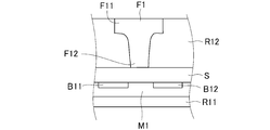
- FIG. 1A shows a partial cross-sectional view taken along the line AA shown in FIG. 1A.
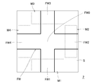
- the MI sensor 1 includes four MI elements M1 to M4 for detecting an external magnetic field such as geomagnetism, a substantially frustoconical magnet collecting yokes F1 to F4 (magnetic field redirectors), and a pulse transmission circuit (drive) on a Si substrate.
- Circuit board S (corresponding to “substrate” in the present invention) on which an integrated circuit (ASIC: application specific integrated circuit) including a circuit), a signal processing circuit, an arithmetic circuit, and the like is formed, and upper and lower surfaces of the circuit board S Insulating resin layers R11 and R12 formed respectively.
- ASIC application specific integrated circuit
- bumps B11 and B12 are formed around the MI element M1 in order to realize a wafer level CSP in which wire bonding for electrical connection between the integrated circuit and the MI element is omitted. Yes.
- each circuit or the like is formed by photolithography.
- MI elements M1 to M4 are mounted on a circuit board S in a square shape by flip chip in order to detect a three-dimensional component of an external magnetic field.
- Magnetic elements in the X-axis direction (simply referred to as “X component”) are detected by MI elements M1 and M3 mounted in parallel in the X-axis direction, and MI elements M2 and M4 mounted in parallel in the Y-axis direction.
- a magnetic component in the Y-axis direction (simply referred to as “Y component”) can be detected.
- Magnetic collecting yokes F1 to F4 are provided on the back side of the circuit board S corresponding to each central position of the MI elements M1 to M4. Since the MI elements M1 to M4 and the magnetism collecting yokes F1 to F4 are the same, the MI element M1 and the magnetism collecting yoke F1 will be described as a representative as appropriate, and the other MI elements M2 to M4 will be described below. A description of M4 and the magnetic flux collecting yokes F2 to F4 is omitted.
- Converged magnetic flux lines of the external magnetic field pass through the circuit board S from the front end surface of the reduced portion F12 and diffuse radially (equally in the left-right direction) from the center of the MI element M1. (See FIG. 5). At that time, if another magnetic field changing body is provided in the vicinity of both ends of the MI element M1 on the opposite side (lower side in FIG. 5) of the circuit board S with respect to the magnetic collecting yoke F1 (see FIG. 10 described later). The magnetic flux lines diffused from the reduced portion F12 of the magnetic flux collecting yoke F1 can be further changed in the wire axis direction of the MI element M1.
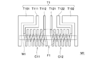
- the MI element M1 includes a magnetic sensing wire W1, a detection coil C1 wound around the magnetic sensing wire W1, and a terminal group T1 connected to the magnetic sensing wire W1 and the detection coil C1.
- the magnetosensitive wire W1 is a zero magnetostrictive amorphous wire made of a Co—Fe—Si—B alloy.
- the detection coil C1 includes a left coil part C11 and a right coil part C12.
- the left coil portion C11 and the right coil portion C12 have the same specifications that affect the output size, such as the number of turns, the winding diameter, the winding direction, and the pitch, and the center position (points) through which the central axis of the magnetism collecting yoke F1 passes. ).
- Each coil part C11, C12 and terminal group T1 are formed on the circuit board S using photolithography.
- the terminal group T1 includes terminals T101 and T102 for supplying pulse signals to the magnetosensitive wire W1, terminals T111 and T112 for outputting electromotive force generated in the left coil part C11, and electromotive force generated in the right coil part C12. Terminal T121 and T122.
- the integrated circuit (ASIC) formed on the circuit board S includes a pulse transmission circuit (driving circuit) that supplies a pulse signal to the magnetosensitive wire W1, and an output (voltage) from the left coil portion C11.
- a signal processing circuit for obtaining V11 and an output (voltage) V12 from the right coil portion C12 and an arithmetic circuit (including a switching circuit) are included.
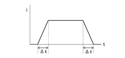
- the pulse transmission circuit and signal processing circuit operate as follows. First, a high-frequency (for example, equivalent to 200 MHz) pulse current generated by the pulse oscillation circuit is supplied to the magnetosensitive wire W1. The magnetic field generated in the wire circumferential direction of the magnetosensitive wire W1 by this pulse current and the external magnetic field act, and a voltage corresponding to the magnetic component acting in the axial direction is generated in the left coil part C11 and the right coil part C12. To do. Note that the frequency here is obtained by calculating the “rise” or “fall” time ⁇ t of the pulse current waveform pulse shown in FIG. 4A, and that ⁇ t corresponds to a quarter period as shown in FIG. 4B. It is a thing.
- a high-frequency (for example, equivalent to 200 MHz) pulse current generated by the pulse oscillation circuit is supplied to the magnetosensitive wire W1.
- the magnetic field generated in the wire circumferential direction of the magnetosensitive wire W1 by this pulse current and the external magnetic field act, and a voltage corresponding to the magnetic component acting
- the analog switch is turned on and off for a short time at a predetermined timing. Accordingly, the analog switch samples each voltage generated in the left coil portion C11 and the right coil portion C12. The sampling voltages are respectively amplified by amplifiers to obtain outputs V11 and V12. It is also possible to obtain V11 and V12 by processing when the pulse current is interrupted instead of rising (when the pulse current falls).
- the arithmetic circuit alternately calculates the sum and difference of the output V11 and the output V12, performs an output indicating the X component of the external magnetic field based on the sum of the output V11 and the output V12, and outputs an external signal based on the difference between the output V11 and the output V12.
- An output indicating the Z component of the magnetic field is performed. The reason why an output indicating the X component and the Z component by the sum and difference can be performed will be described below.
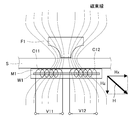
- a magnetic flux line (magnetic line) of an external magnetic field generated around the MI element M1 can be changed in each direction by the magnetic flux collecting yoke F1.
- the magnetic flux lines of the Z component (direction component orthogonal to the circuit board S) of the external magnetic field are largely changed by the magnetic collecting yoke F1 as shown in FIG.
- the magnetic flux collecting yoke F1 is arranged at the center of the symmetrical left coil portion C11 and the right coil portion C12 of the MI element M1, the influence on the output appearing in each coil portion due to the change of the external magnetic field is also symmetrical. It becomes.
- the turning magnetic component (measured magnetic field / magnetic vector H) which is the Z component of the external magnetic field redirected by the magnetic flux collecting yoke F1
- the left coil portion C11 and the right coil portion C12 output as described above. Since the specifications that affect the size of the coil are all the same, the output difference (V11 ⁇ V12) between the output V11 of the left coil part C11 and the output V12 of the right coil part C12 occurs around the MI element M1.
- the influence of the component in the X-axis direction of the original external magnetic field is canceled, and only the influence of the further X component (Hx) of the deflection magnetic component acting in the opposite direction on the left coil portion C11 and the right coil portion C12 is reflected. It will be.
- the Z component (Hz) of the turning magnetic component does not respond to the magnetosensitive wire W1, and naturally does not affect the output difference. If the output difference is multiplied by an appropriate coefficient, the Z component of the original external magnetic field can be obtained from the output difference.
- the output sum (V11 + V12) of the output V11 and the output V12 cancels the influence of the X component (Hx) of the turning magnetic component, and does not have the influence of the Z component (Hz) of the turning magnetic component as described above. Only the influence of a further X component (projection component in the X-axis direction) of the magnetic component generated by redirecting the X component of the original external magnetic field by the magnetic collecting yoke F1 is reflected. If the output sum is multiplied by an appropriate coefficient, the X component of the original external magnetic field can be obtained from the output sum. Such a situation also applies to the MI element M3. Further, with the same concept, the Y component and the Z component can be detected by the MI element M2 and the MI element M4.
- the component in each axial direction of the external magnetic field is calculated based on an average value (for example, an arithmetic average) of outputs of a plurality of MI elements without depending on only the output of one MI element.
- an appropriate correction coefficient or correction term can be added to the output value in consideration of the shape of the magnetic flux collecting yoke, the arrangement and characteristics of the MI element, and the like.
- Such arithmetic processing may be performed by the arithmetic circuit described above, or may be performed by a program such as an information terminal in which the MI sensor 1 is mounted. The basic concept regarding the arithmetic processing is also described in detail in WO2010 / 110456.
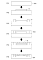
- FIGS. Each manufacturing process of the MI sensor 1 is shown in FIGS.
- a base substrate SB0 in which a large number of integrated circuits including the above-described pulse oscillation circuit, signal processing circuit, and arithmetic circuit are formed on a silicon wafer is prepared (process P11).
- a large number of MI elements M are mounted by flip chip at predetermined positions on one surface side of the base substrate SB0 (process P12).
- a Cu post Q for power supply for integrated circuits and communication input / output is formed on the base substrate SB0 by photolithography (process P13), and the surface is covered and filled with an insulating resin RB1 (process P14).
- a bump B for connection to an external circuit is formed (process P15).
- the other surface side of the base substrate SB0 is polished (back grind) to obtain the mounting base substrate SB1 (step P16).
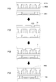
- a soft magnetic plate FB made of permalloy alloy corresponding to the size of the mounting base substrate SB1 is prepared (step P21).
- the soft magnetic plate FB is half-etched using photolithography (process P22). During this etching, the surface portion of the eroded soft magnetic plate FB is eroded into a tapered shape having a wider surface side and a narrower interior. For this reason, a turning body pattern in which a large number of frustoconical islands F0 having a reduced portion F02 formed on the surface side and an enlarged portion F01 formed on the inner side is naturally formed.
- a deflector pattern plate FP is obtained in which a large number of truncated cone islands F0 are connected by the remaining portion F03 of the soft magnetic plate FB.
- An insulating resin RB2 is filled on the pattern surface side of the deflector pattern plate FP, and the surface thereof is flattened (process P23).
- the deflector pattern plate FP1 filled with the resin is obtained.
- the other surface side of the mounting base substrate SB1 obtained through the above-described steps and the pattern surface side of the deflector pattern plate FP1 filled with the resin are accurately aligned and opposed to each other.
- bonding is performed via the insulating resin RB2 (process P31 / bonding process).
- a resist rg is formed by photolithography on the other surface side (the opposite surface side of the pattern surface side) of the deflector pattern plate FP1 (process P32).
- the remaining portion F03 of the deflector pattern plate FP1 is removed by etching (process P33 / separation process).
- the magnetism collecting yoke F having the enlarged portion and the reduced portion is arranged at the center of each MI element. Furthermore, the insulating resin RB2 is further filled to flatten the surface (process P34). In this way, a bonded base substrate SU (union base substrate) having a large number of MI sensors in which a large number of MI elements M and magnetic collecting yokes F are accurately arranged is obtained. By dicing the bonded base substrate SU, a large number of MI sensors 1 can be obtained at one time (dividing step). In this embodiment, an example is shown in which the magnetic collecting yoke F is manufactured by etching the remaining portion at the bonding value. However, a plate on which a large number of magnetic collecting yokes F divided in the same process before the bonding are arranged is arranged. It may be produced and then joined.
- FIG. 9 shows the MI sensor 2 in which the magnetism collecting yoke FW in which the shape of the magnetism collecting yoke F1 of the first embodiment is changed is arranged.
- symbol is attached
- the magnetism collecting yoke FW of the MI sensor 2 has a cross shape and is arranged at the center of the other surface side of the circuit board S.
- the extending portions FW1 to FW4 of the magnetic flux collecting yoke FW are located at the respective central positions of the MI elements M1 to M4, and the magnetic flux collecting yoke FW has an integrated structure in which they are connected at the central portion FW0. .
- Such a symmetrical magnetism collecting yoke FW can perform the same function as the magnetism collecting yoke F1 and the like.
- the MI sensor 2 provided with the magnetism collecting yoke FW is also a redirecting body pattern plate in which many square-shaped depressions are formed in the soft magnetic plate FB made of permalloy alloy by half etching instead of the above-mentioned turning body pattern plate FP1.
- FP ′ (not shown), it can be produced efficiently.
- FIG. 10 shows the MI sensor 3 in which the magnetism collecting yoke Fs, in which the magnetism collecting yoke F1 is miniaturized, is arranged near both ends of the circuit board S on the MI element M1 side.
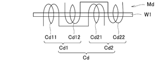
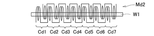
- FIG. 11A shows an MI sensor 4 in which two magnetism collecting yokes Fs1 and Fs2 in which the magnetism collecting yoke F1 is miniaturized are evenly arranged in the middle of the MI element Md.
- the detection coil Cd of the MI sensor 4 includes divided coil portions Cd1 and Cd2 that are divided into two units.
- the split coil portion Cd1 includes a left split coil portion Cd11 and a right split coil portion Cd12
- the split coil portion Cd2 includes a left split coil portion Cd21 and a right split coil portion Cd22.
- the magnetic collecting yoke Fs1 is disposed in the center of the divided coil portion Cd1, that is, between the left divided coil portion Cd11 and the right divided coil portion Cd12. Arranged between the right split coil portion Cd22. According to the MI sensor 4, the Z component of the external magnetic field can be detected with high sensitivity while reducing the size.
- the left divided coil portion Cd11 and the left divided coil portion Cd21, and the right divided coil portion Cd12 and the right divided coil portion Cd22 are connected to have the same polarity (winding direction). Although shown as an example, each of the four coil portions may be independent.
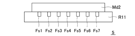
- the detection coil is divided into two to seven divided coil portions Cd 1 to Cd 7, and the magnetic collecting yokes are set to seven magnetic collecting yokes Fs 1 to Fs 7, thereby further reducing the size and thickness of the MI sensor 5. Is shown in FIGS. 12A and 12B.
- FIG. 13 shows an MI sensor 6 in which the circuit board S described above is changed to a built-in circuit board S2 (corresponding to “substrate” in the present invention) having a built-in magnetic collecting yoke Fi.
- the magnetic collecting yoke Fi is also made of a permalloy alloy and has a large-diameter disk-shaped enlarged portion Fi1 and a columnar reduced portion Fi2 extending from the enlarged portion Fi1.
- the effects of the magnetic collecting yoke Fi and the operation of the MI sensor 6 are the same as those of the MI sensor 1.
- the distance between the magnetic collecting yoke Fi and the MI element M can be made closer than the MI sensor 1 shown in FIG.
- the MI sensor itself can be further reduced in thickness and size, but also its sensitivity can be improved.
- the output (sensitivity) of the MI sensor is about 3.5 times as much.
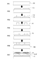
- the built-in circuit board S2 is manufactured through, for example, the steps shown in FIG. First, a Si substrate S0 made of a silicon wafer is prepared (process P61). The Si substrate S0 is the same as the Si substrate used to manufacture the circuit substrate S.
- a first plating layer of a permalloy alloy to be the enlarged portion Fi1 is formed on the Si substrate S0 (process P62).
- a second plating layer of a permalloy alloy that becomes the reduced portion Fi2 is formed on the first plating layer (process P63).
- the enlarged portion Fi1 and the reduced portion Fi2 thus laminated are heat-treated (annealed) (process P64).
- the internal stress introduced into the enlarged portion Fi1 and the reduced portion Fi2 in each plating step is removed, and a magnetic flux collecting yoke Fi composed of the enlarged portion Fi1 and the reduced portion Fi2 having excellent soft magnetic characteristics is obtained.
- An insulating resin layer Ri surrounding the magnetic flux collecting yoke Fi formed on the Si substrate S0 is formed by a resin mold (process P65).
- the upper end surface of the insulating resin layer Ri is polished and flattened (process P66).
- a circuit necessary for driving the MI sensor 6 is formed between the heat treatment process (process P64) and the polishing process (process P66). In this way, the built-in base substrate SBi with the built-in magnet collecting yoke Fi is obtained.
- the MI element M is mounted on the built-in base substrate SBi by flip chip or the like (process P67 / mounting process). Thereafter, the respective steps as shown in FIG. 6 are performed to polish (back grind) one side of the built-in base substrate SBi (the other side of the Si substrate S0). In this way, the combined base substrate SU2 is obtained.
- a large number of MI sensors 6 are obtained by dicing the combined base substrate SU2 (dividing step). Each MI sensor may be formed on the surface of the built-in base substrate SBi or the like by a method detailed in WO 2014/054371 or the like.
Abstract
Priority Applications (4)
| Application Number | Priority Date | Filing Date | Title |
|---|---|---|---|
| JP2016517833A JP6222351B2 (ja) | 2014-05-09 | 2015-03-12 | 磁気検出装置およびその製造方法 |
| CN201580023842.1A CN106461739B (zh) | 2014-05-09 | 2015-03-12 | 磁检测装置及其制造方法 |
| US15/305,864 US10048329B2 (en) | 2014-05-09 | 2015-03-12 | Magnetic detection device and method of manufacturing same |
| EP15789848.7A EP3141920B1 (fr) | 2014-05-09 | 2015-03-12 | Dispositif de détection magnétique et son procédé de fabrication |
Applications Claiming Priority (2)
| Application Number | Priority Date | Filing Date | Title |
|---|---|---|---|
| JP2014097251 | 2014-05-09 | ||
| JP2014-097251 | 2014-05-09 |
Publications (1)
| Publication Number | Publication Date |
|---|---|
| WO2015170509A1 true WO2015170509A1 (fr) | 2015-11-12 |
Family
ID=54392363
Family Applications (1)
| Application Number | Title | Priority Date | Filing Date |
|---|---|---|---|
| PCT/JP2015/057237 WO2015170509A1 (fr) | 2014-05-09 | 2015-03-12 | Dispositif de détection magnétique et son procédé de fabrication |
Country Status (5)
| Country | Link |
|---|---|
| US (1) | US10048329B2 (fr) |
| EP (1) | EP3141920B1 (fr) |
| JP (1) | JP6222351B2 (fr) |
| CN (1) | CN106461739B (fr) |
| WO (1) | WO2015170509A1 (fr) |
Cited By (11)
| Publication number | Priority date | Publication date | Assignee | Title |
|---|---|---|---|---|
| JP2017111148A (ja) * | 2015-12-17 | 2017-06-22 | アナログ デバイシス グローバル | 磁気構造を含むデバイス、システム、および方法 |
| WO2017149831A1 (fr) * | 2016-03-03 | 2017-09-08 | Tdk株式会社 | Capteur magnétique |
| JP2017173123A (ja) * | 2016-03-23 | 2017-09-28 | アルプス電気株式会社 | 磁気センサおよびその製造方法 |
| JP6240994B1 (ja) * | 2016-12-15 | 2017-12-06 | 朝日インテック株式会社 | 3次元磁界検出素子および3次元磁界検出装置 |
| CN107976644A (zh) * | 2016-10-25 | 2018-05-01 | Tdk株式会社 | 磁场检测装置 |
| CN108152762A (zh) * | 2016-12-06 | 2018-06-12 | Tdk株式会社 | 磁场检测装置 |
| JP2018128390A (ja) * | 2017-02-09 | 2018-08-16 | Tdk株式会社 | 磁気センサとその製造方法 |
| CN108461627A (zh) * | 2017-02-22 | 2018-08-28 | Tdk株式会社 | 磁传感器及其制造方法 |
| WO2019139110A1 (fr) * | 2018-01-11 | 2019-07-18 | Tdk株式会社 | Capteur magnétique |
| JP2020073905A (ja) * | 2020-01-15 | 2020-05-14 | Tdk株式会社 | 磁気センサ |
| US10813065B2 (en) | 2016-07-01 | 2020-10-20 | Guangdong Oppo Mobile Telecommunications Corp., Ltd. | Method and device for signal detection |
Families Citing this family (6)
| Publication number | Priority date | Publication date | Assignee | Title |
|---|---|---|---|---|
| JP6483435B2 (ja) * | 2014-12-26 | 2019-03-13 | ローム株式会社 | 磁気検出装置 |
| DE102015202871A1 (de) * | 2015-02-18 | 2016-08-18 | Robert Bosch Gmbh | Hallsensor |
| JP6021238B1 (ja) * | 2015-10-11 | 2016-11-09 | マグネデザイン株式会社 | グラジオセンサ素子およびグラジオセンサ |
| JP6661570B2 (ja) * | 2017-05-11 | 2020-03-11 | 矢崎総業株式会社 | 磁界検出センサ |
| WO2019111765A1 (fr) * | 2017-12-04 | 2019-06-13 | 株式会社村田製作所 | Capteur magnétique |
| JP2023002228A (ja) * | 2021-06-22 | 2023-01-10 | 昭和電工株式会社 | 情報処理装置および磁気センサシステム |
Citations (9)
| Publication number | Priority date | Publication date | Assignee | Title |
|---|---|---|---|---|
| JPS4814275U (fr) * | 1971-06-26 | 1973-02-17 | ||
| JPS63152185A (ja) * | 1986-12-16 | 1988-06-24 | Sharp Corp | 感磁性半導体装置の製造方法 |
| JPH1022545A (ja) * | 1996-07-02 | 1998-01-23 | Sankyo Seiki Mfg Co Ltd | 磁電変換装置 |
| JP2001013231A (ja) * | 1999-05-12 | 2001-01-19 | Asulab Sa | 半導体基板上に形成された磁気センサ |
| JP2008134236A (ja) * | 2006-10-25 | 2008-06-12 | Aichi Steel Works Ltd | 磁気検出器 |
| JP2010101648A (ja) * | 2008-10-21 | 2010-05-06 | Asahi Kasei Electronics Co Ltd | 磁気センサ |
| WO2010110456A1 (fr) * | 2009-03-26 | 2010-09-30 | 愛知製鋼株式会社 | Dispositif de détection magnétique |
| JP5066576B2 (ja) * | 2007-10-11 | 2012-11-07 | アルプス電気株式会社 | 磁気検出装置 |
| JP2014153309A (ja) * | 2013-02-13 | 2014-08-25 | Magne Design Corp | 磁界検出素子 |
Family Cites Families (13)
| Publication number | Priority date | Publication date | Assignee | Title |
|---|---|---|---|---|
| JPWO2003009403A1 (ja) * | 2001-07-19 | 2004-11-11 | 松下電器産業株式会社 | 磁気センサ及びその製造方法 |
| WO2004013645A1 (fr) * | 2002-08-01 | 2004-02-12 | Sentron Ag | Capteur de champ magnetique et procede pour faire fonctionner un tel capteur |
| KR100536837B1 (ko) * | 2003-02-10 | 2005-12-16 | 삼성전자주식회사 | 반도체기판에 집적된 자계검출소자 및 그 제조방법 |
| JP3781056B2 (ja) | 2003-07-18 | 2006-05-31 | 愛知製鋼株式会社 | 3次元磁気方位センサおよびマグネト・インピーダンス・センサ素子 |
| US7509748B2 (en) * | 2006-09-01 | 2009-03-31 | Seagate Technology Llc | Magnetic MEMS sensors |
| CN103454601B (zh) * | 2008-03-28 | 2016-05-18 | 爱知制钢株式会社 | 磁敏线、磁阻抗元件及磁阻抗传感器 |
| WO2010097932A1 (fr) * | 2009-02-27 | 2010-09-02 | 愛知製鋼株式会社 | Élément capteur à magnéto-impédance et son procédé de fabrication |
| US8922205B2 (en) * | 2011-10-31 | 2014-12-30 | Everspin Technologies, Inc. | Apparatus and method for reset and stabilization control of a magnetic sensor |
| US8680854B2 (en) * | 2011-12-01 | 2014-03-25 | Texas Instruments Incorporated | Semiconductor GMI magnetometer |
| US9488496B2 (en) * | 2012-09-13 | 2016-11-08 | Bourns, Inc. | Position measurement using flux modulation and angle sensing |
| US20150262748A1 (en) | 2012-10-04 | 2015-09-17 | Aichi Steel Corporation | Magneto-impedance element and method for producing the same |
| US9116179B2 (en) * | 2012-12-17 | 2015-08-25 | Covidien Lp | System and method for voltage and current sensing |
| CN103323795B (zh) * | 2013-06-21 | 2015-04-08 | 中国人民解放军国防科学技术大学 | 一体式三轴磁传感器 |
-
2015
- 2015-03-12 CN CN201580023842.1A patent/CN106461739B/zh active Active
- 2015-03-12 EP EP15789848.7A patent/EP3141920B1/fr active Active
- 2015-03-12 JP JP2016517833A patent/JP6222351B2/ja active Active
- 2015-03-12 US US15/305,864 patent/US10048329B2/en active Active
- 2015-03-12 WO PCT/JP2015/057237 patent/WO2015170509A1/fr active Application Filing
Patent Citations (9)
| Publication number | Priority date | Publication date | Assignee | Title |
|---|---|---|---|---|
| JPS4814275U (fr) * | 1971-06-26 | 1973-02-17 | ||
| JPS63152185A (ja) * | 1986-12-16 | 1988-06-24 | Sharp Corp | 感磁性半導体装置の製造方法 |
| JPH1022545A (ja) * | 1996-07-02 | 1998-01-23 | Sankyo Seiki Mfg Co Ltd | 磁電変換装置 |
| JP2001013231A (ja) * | 1999-05-12 | 2001-01-19 | Asulab Sa | 半導体基板上に形成された磁気センサ |
| JP2008134236A (ja) * | 2006-10-25 | 2008-06-12 | Aichi Steel Works Ltd | 磁気検出器 |
| JP5066576B2 (ja) * | 2007-10-11 | 2012-11-07 | アルプス電気株式会社 | 磁気検出装置 |
| JP2010101648A (ja) * | 2008-10-21 | 2010-05-06 | Asahi Kasei Electronics Co Ltd | 磁気センサ |
| WO2010110456A1 (fr) * | 2009-03-26 | 2010-09-30 | 愛知製鋼株式会社 | Dispositif de détection magnétique |
| JP2014153309A (ja) * | 2013-02-13 | 2014-08-25 | Magne Design Corp | 磁界検出素子 |
Non-Patent Citations (1)
| Title |
|---|
| See also references of EP3141920A4 * |
Cited By (30)
| Publication number | Priority date | Publication date | Assignee | Title |
|---|---|---|---|---|
| US10145906B2 (en) | 2015-12-17 | 2018-12-04 | Analog Devices Global | Devices, systems and methods including magnetic structures |
| CN106896333A (zh) * | 2015-12-17 | 2017-06-27 | 亚德诺半导体集团 | 包括磁性结构的设备、系统和方法 |
| US11649157B2 (en) | 2015-12-17 | 2023-05-16 | Analog Devices International Unlimited Company | Devices, systems and methods including magnetic structures and micromechanical structure |
| US11061086B2 (en) | 2015-12-17 | 2021-07-13 | Analog Devices Global | Magnetic device with magnetic structure and micro-fluidic structure |
| JP2017111148A (ja) * | 2015-12-17 | 2017-06-22 | アナログ デバイシス グローバル | 磁気構造を含むデバイス、システム、および方法 |
| US10429456B2 (en) | 2015-12-17 | 2019-10-01 | Analog Devices Global | Modules and methods including magnetic sensing structures |
| WO2017149831A1 (fr) * | 2016-03-03 | 2017-09-08 | Tdk株式会社 | Capteur magnétique |
| JP2017161519A (ja) * | 2016-03-03 | 2017-09-14 | Tdk株式会社 | 磁気センサ |
| JP2017173123A (ja) * | 2016-03-23 | 2017-09-28 | アルプス電気株式会社 | 磁気センサおよびその製造方法 |
| US10813065B2 (en) | 2016-07-01 | 2020-10-20 | Guangdong Oppo Mobile Telecommunications Corp., Ltd. | Method and device for signal detection |
| CN107976644A (zh) * | 2016-10-25 | 2018-05-01 | Tdk株式会社 | 磁场检测装置 |
| US10732232B2 (en) | 2016-12-06 | 2020-08-04 | Tdk Corporation | Magnetic field detection device |
| US11703551B2 (en) | 2016-12-06 | 2023-07-18 | Tdk Corporation | Magnetic field detection device |
| CN108152762B (zh) * | 2016-12-06 | 2021-03-05 | Tdk株式会社 | 磁场检测装置 |
| CN108152762A (zh) * | 2016-12-06 | 2018-06-12 | Tdk株式会社 | 磁场检测装置 |
| US11353518B2 (en) | 2016-12-06 | 2022-06-07 | Tdk Corporation | Magnetic field detection device |
| JP2018091784A (ja) * | 2016-12-06 | 2018-06-14 | Tdk株式会社 | 磁場検出装置 |
| JP6240994B1 (ja) * | 2016-12-15 | 2017-12-06 | 朝日インテック株式会社 | 3次元磁界検出素子および3次元磁界検出装置 |
| KR102312092B1 (ko) | 2016-12-15 | 2021-10-14 | 아사히 인텍크 가부시키가이샤 | 3차원 자계 검출 소자 및 3차원 자계 검출 장치 |
| JP2018096885A (ja) * | 2016-12-15 | 2018-06-21 | 朝日インテック株式会社 | 3次元磁界検出素子および3次元磁界検出装置 |
| US10634740B2 (en) | 2017-02-09 | 2020-04-28 | Tdk Corporation | Magnetic sensor and method of manufacturing the same |
| JP2018128390A (ja) * | 2017-02-09 | 2018-08-16 | Tdk株式会社 | 磁気センサとその製造方法 |
| CN108414954A (zh) * | 2017-02-09 | 2018-08-17 | Tdk株式会社 | 磁传感器及其制造方法 |
| US11067648B2 (en) | 2017-02-22 | 2021-07-20 | Tdk Corporation | Magnetic sensor and method of manufacturing the same |
| US10527687B2 (en) | 2017-02-22 | 2020-01-07 | Tdk Corporation | Magnetic sensor and method of manufacturing the same |
| JP2018136212A (ja) * | 2017-02-22 | 2018-08-30 | Tdk株式会社 | 磁気センサとその製造方法 |
| CN108461627A (zh) * | 2017-02-22 | 2018-08-28 | Tdk株式会社 | 磁传感器及其制造方法 |
| JPWO2019139110A1 (ja) * | 2018-01-11 | 2021-01-28 | Tdk株式会社 | 磁気センサ |
| WO2019139110A1 (fr) * | 2018-01-11 | 2019-07-18 | Tdk株式会社 | Capteur magnétique |
| JP2020073905A (ja) * | 2020-01-15 | 2020-05-14 | Tdk株式会社 | 磁気センサ |
Also Published As
| Publication number | Publication date |
|---|---|
| EP3141920B1 (fr) | 2021-04-14 |
| JPWO2015170509A1 (ja) | 2017-04-20 |
| CN106461739B (zh) | 2019-06-07 |
| EP3141920A1 (fr) | 2017-03-15 |
| EP3141920A4 (fr) | 2018-01-03 |
| CN106461739A (zh) | 2017-02-22 |
| US10048329B2 (en) | 2018-08-14 |
| US20170160351A1 (en) | 2017-06-08 |
| JP6222351B2 (ja) | 2017-11-01 |
Similar Documents
| Publication | Publication Date | Title |
|---|---|---|
| JP6222351B2 (ja) | 磁気検出装置およびその製造方法 | |
| JP4626728B2 (ja) | 磁気検出装置 | |
| JP6036938B1 (ja) | 磁気検出装置 | |
| US11009566B2 (en) | Three-dimensional magnetic field detection element and three-dimensional magnetic field detection device | |
| JP6021239B2 (ja) | 3次元磁界検出素子および3次元磁界検出装置 | |
| JP2008506946A (ja) | 直流電流センサー | |
| JP2014153309A5 (fr) | ||
| JP6609947B2 (ja) | 磁気検出装置 | |
| JP2020160081A (ja) | 3次元磁界検出装置 | |
| JP6800456B2 (ja) | 3次元磁界検出素子および3次元磁界検出装置 | |
| TWI457583B (zh) | Three - axis magnetic field sensing device with magnetic flux guide | |
| Liakopoulos et al. | A micro fluxgate magnetic sensor using micromachined 3-dimensional planar coils | |
| JP2016003866A (ja) | Z軸用gmi素子および超薄型3次元gmiセンサ | |
| JP6222897B2 (ja) | 多軸磁気センサ、および、その製造方法 |
Legal Events
| Date | Code | Title | Description |
|---|---|---|---|
| 121 | Ep: the epo has been informed by wipo that ep was designated in this application |
Ref document number: 15789848 Country of ref document: EP Kind code of ref document: A1 |
|
| ENP | Entry into the national phase |
Ref document number: 2016517833 Country of ref document: JP Kind code of ref document: A |
|
| REEP | Request for entry into the european phase |
Ref document number: 2015789848 Country of ref document: EP |
|
| WWE | Wipo information: entry into national phase |
Ref document number: 2015789848 Country of ref document: EP |
|
| WWE | Wipo information: entry into national phase |
Ref document number: 15305864 Country of ref document: US |
|
| NENP | Non-entry into the national phase |
Ref country code: DE |