WO2015156381A1 - 半導体基板の処理方法及び該処理方法を用いる半導体装置の製造方法 - Google Patents
半導体基板の処理方法及び該処理方法を用いる半導体装置の製造方法 Download PDFInfo
- Publication number
- WO2015156381A1 WO2015156381A1 PCT/JP2015/061188 JP2015061188W WO2015156381A1 WO 2015156381 A1 WO2015156381 A1 WO 2015156381A1 JP 2015061188 W JP2015061188 W JP 2015061188W WO 2015156381 A1 WO2015156381 A1 WO 2015156381A1
- Authority
- WO
- WIPO (PCT)
- Prior art keywords
- semiconductor substrate
- layer
- support plate
- bonding
- amorphous
- Prior art date
- Legal status (The legal status is an assumption and is not a legal conclusion. Google has not performed a legal analysis and makes no representation as to the accuracy of the status listed.)
- Ceased
Links
Images


Classifications
-
- H—ELECTRICITY
- H10—SEMICONDUCTOR DEVICES; ELECTRIC SOLID-STATE DEVICES NOT OTHERWISE PROVIDED FOR
- H10W—GENERIC PACKAGES, INTERCONNECTIONS, CONNECTORS OR OTHER CONSTRUCTIONAL DETAILS OF DEVICES COVERED BY CLASS H10
- H10W70/00—Package substrates; Interposers; Redistribution layers [RDL]
- H10W70/01—Manufacture or treatment
- H10W70/02—Manufacture or treatment of conductive package substrates serving as an interconnection, e.g. of metal plates
-
- H—ELECTRICITY
- H10—SEMICONDUCTOR DEVICES; ELECTRIC SOLID-STATE DEVICES NOT OTHERWISE PROVIDED FOR
- H10D—INORGANIC ELECTRIC SEMICONDUCTOR DEVICES
- H10D12/00—Bipolar devices controlled by the field effect, e.g. insulated-gate bipolar transistors [IGBT]
- H10D12/01—Manufacture or treatment
- H10D12/031—Manufacture or treatment of IGBTs
-
- H—ELECTRICITY
- H10—SEMICONDUCTOR DEVICES; ELECTRIC SOLID-STATE DEVICES NOT OTHERWISE PROVIDED FOR
- H10D—INORGANIC ELECTRIC SEMICONDUCTOR DEVICES
- H10D30/00—Field-effect transistors [FET]
- H10D30/01—Manufacture or treatment
- H10D30/021—Manufacture or treatment of FETs having insulated gates [IGFET]
- H10D30/028—Manufacture or treatment of FETs having insulated gates [IGFET] of double-diffused metal oxide semiconductor [DMOS] FETs
- H10D30/0291—Manufacture or treatment of FETs having insulated gates [IGFET] of double-diffused metal oxide semiconductor [DMOS] FETs of vertical DMOS [VDMOS] FETs
-
- H—ELECTRICITY
- H10—SEMICONDUCTOR DEVICES; ELECTRIC SOLID-STATE DEVICES NOT OTHERWISE PROVIDED FOR
- H10D—INORGANIC ELECTRIC SEMICONDUCTOR DEVICES
- H10D62/00—Semiconductor bodies, or regions thereof, of devices having potential barriers
- H10D62/40—Crystalline structures
- H10D62/405—Orientations of crystalline planes
-
- H—ELECTRICITY
- H10—SEMICONDUCTOR DEVICES; ELECTRIC SOLID-STATE DEVICES NOT OTHERWISE PROVIDED FOR
- H10D—INORGANIC ELECTRIC SEMICONDUCTOR DEVICES
- H10D62/00—Semiconductor bodies, or regions thereof, of devices having potential barriers
- H10D62/80—Semiconductor bodies, or regions thereof, of devices having potential barriers characterised by the materials
- H10D62/83—Semiconductor bodies, or regions thereof, of devices having potential barriers characterised by the materials being Group IV materials, e.g. B-doped Si or undoped Ge
- H10D62/832—Semiconductor bodies, or regions thereof, of devices having potential barriers characterised by the materials being Group IV materials, e.g. B-doped Si or undoped Ge being Group IV materials comprising two or more elements, e.g. SiGe
- H10D62/8325—Silicon carbide
-
- H—ELECTRICITY
- H10—SEMICONDUCTOR DEVICES; ELECTRIC SOLID-STATE DEVICES NOT OTHERWISE PROVIDED FOR
- H10D—INORGANIC ELECTRIC SEMICONDUCTOR DEVICES
- H10D62/00—Semiconductor bodies, or regions thereof, of devices having potential barriers
- H10D62/80—Semiconductor bodies, or regions thereof, of devices having potential barriers characterised by the materials
- H10D62/85—Semiconductor bodies, or regions thereof, of devices having potential barriers characterised by the materials being Group III-V materials, e.g. GaAs
- H10D62/8503—Nitride Group III-V materials, e.g. AlN or GaN
-
- H—ELECTRICITY
- H10—SEMICONDUCTOR DEVICES; ELECTRIC SOLID-STATE DEVICES NOT OTHERWISE PROVIDED FOR
- H10D—INORGANIC ELECTRIC SEMICONDUCTOR DEVICES
- H10D64/00—Electrodes of devices having potential barriers
- H10D64/01—Manufacture or treatment
- H10D64/011—Manufacture or treatment of electrodes ohmically coupled to a semiconductor
-
- H—ELECTRICITY
- H10—SEMICONDUCTOR DEVICES; ELECTRIC SOLID-STATE DEVICES NOT OTHERWISE PROVIDED FOR
- H10D—INORGANIC ELECTRIC SEMICONDUCTOR DEVICES
- H10D64/00—Electrodes of devices having potential barriers
- H10D64/01—Manufacture or treatment
- H10D64/011—Manufacture or treatment of electrodes ohmically coupled to a semiconductor
- H10D64/0111—Manufacture or treatment of electrodes ohmically coupled to a semiconductor to Group IV semiconductors
- H10D64/0115—Manufacture or treatment of electrodes ohmically coupled to a semiconductor to Group IV semiconductors to silicon carbide
-
- H—ELECTRICITY
- H10—SEMICONDUCTOR DEVICES; ELECTRIC SOLID-STATE DEVICES NOT OTHERWISE PROVIDED FOR
- H10P—GENERIC PROCESSES OR APPARATUS FOR THE MANUFACTURE OR TREATMENT OF DEVICES COVERED BY CLASS H10
- H10P14/00—Formation of materials, e.g. in the shape of layers or pillars
- H10P14/20—Formation of materials, e.g. in the shape of layers or pillars of semiconductor materials
- H10P14/32—Formation of materials, e.g. in the shape of layers or pillars of semiconductor materials characterised by intermediate layers between substrates and deposited layers
- H10P14/3202—Materials thereof
- H10P14/3204—Materials thereof being Group IVA semiconducting materials
- H10P14/3211—Silicon, silicon germanium or germanium
-
- H—ELECTRICITY
- H10—SEMICONDUCTOR DEVICES; ELECTRIC SOLID-STATE DEVICES NOT OTHERWISE PROVIDED FOR
- H10P—GENERIC PROCESSES OR APPARATUS FOR THE MANUFACTURE OR TREATMENT OF DEVICES COVERED BY CLASS H10
- H10P14/00—Formation of materials, e.g. in the shape of layers or pillars
- H10P14/20—Formation of materials, e.g. in the shape of layers or pillars of semiconductor materials
- H10P14/32—Formation of materials, e.g. in the shape of layers or pillars of semiconductor materials characterised by intermediate layers between substrates and deposited layers
- H10P14/3242—Structure
- H10P14/3244—Layer structure
- H10P14/3251—Layer structure consisting of three or more layers
-
- H—ELECTRICITY
- H10—SEMICONDUCTOR DEVICES; ELECTRIC SOLID-STATE DEVICES NOT OTHERWISE PROVIDED FOR
- H10P—GENERIC PROCESSES OR APPARATUS FOR THE MANUFACTURE OR TREATMENT OF DEVICES COVERED BY CLASS H10
- H10P72/00—Handling or holding of wafers, substrates or devices during manufacture or treatment thereof
- H10P72/70—Handling or holding of wafers, substrates or devices during manufacture or treatment thereof for supporting or gripping
- H10P72/74—Handling or holding of wafers, substrates or devices during manufacture or treatment thereof for supporting or gripping using temporarily an auxiliary support
-
- H—ELECTRICITY
- H10—SEMICONDUCTOR DEVICES; ELECTRIC SOLID-STATE DEVICES NOT OTHERWISE PROVIDED FOR
- H10P—GENERIC PROCESSES OR APPARATUS FOR THE MANUFACTURE OR TREATMENT OF DEVICES COVERED BY CLASS H10
- H10P72/00—Handling or holding of wafers, substrates or devices during manufacture or treatment thereof
- H10P72/70—Handling or holding of wafers, substrates or devices during manufacture or treatment thereof for supporting or gripping
- H10P72/74—Handling or holding of wafers, substrates or devices during manufacture or treatment thereof for supporting or gripping using temporarily an auxiliary support
- H10P72/7448—Handling or holding of wafers, substrates or devices during manufacture or treatment thereof for supporting or gripping using temporarily an auxiliary support the bond interface between the auxiliary support and the wafer comprising two or more, e.g. multilayer adhesive or adhesive and release layer
-
- H—ELECTRICITY
- H10—SEMICONDUCTOR DEVICES; ELECTRIC SOLID-STATE DEVICES NOT OTHERWISE PROVIDED FOR
- H10P—GENERIC PROCESSES OR APPARATUS FOR THE MANUFACTURE OR TREATMENT OF DEVICES COVERED BY CLASS H10
- H10P90/00—Preparation of wafers not covered by a single main group of this subclass, e.g. wafer reinforcement
- H10P90/19—Preparing inhomogeneous wafers
- H10P90/1904—Preparing vertically inhomogeneous wafers
- H10P90/1906—Preparing SOI wafers
- H10P90/1914—Preparing SOI wafers using bonding
-
- H—ELECTRICITY
- H10—SEMICONDUCTOR DEVICES; ELECTRIC SOLID-STATE DEVICES NOT OTHERWISE PROVIDED FOR
- H10P—GENERIC PROCESSES OR APPARATUS FOR THE MANUFACTURE OR TREATMENT OF DEVICES COVERED BY CLASS H10
- H10P95/00—Generic processes or apparatus for manufacture or treatments not covered by the other groups of this subclass
- H10P95/90—Thermal treatments, e.g. annealing or sintering
-
- H—ELECTRICITY
- H10—SEMICONDUCTOR DEVICES; ELECTRIC SOLID-STATE DEVICES NOT OTHERWISE PROVIDED FOR
- H10P—GENERIC PROCESSES OR APPARATUS FOR THE MANUFACTURE OR TREATMENT OF DEVICES COVERED BY CLASS H10
- H10P72/00—Handling or holding of wafers, substrates or devices during manufacture or treatment thereof
- H10P72/70—Handling or holding of wafers, substrates or devices during manufacture or treatment thereof for supporting or gripping
- H10P72/74—Handling or holding of wafers, substrates or devices during manufacture or treatment thereof for supporting or gripping using temporarily an auxiliary support
- H10P72/7416—Handling or holding of wafers, substrates or devices during manufacture or treatment thereof for supporting or gripping using temporarily an auxiliary support used during dicing or grinding
-
- H—ELECTRICITY
- H10—SEMICONDUCTOR DEVICES; ELECTRIC SOLID-STATE DEVICES NOT OTHERWISE PROVIDED FOR
- H10P—GENERIC PROCESSES OR APPARATUS FOR THE MANUFACTURE OR TREATMENT OF DEVICES COVERED BY CLASS H10
- H10P72/00—Handling or holding of wafers, substrates or devices during manufacture or treatment thereof
- H10P72/70—Handling or holding of wafers, substrates or devices during manufacture or treatment thereof for supporting or gripping
- H10P72/74—Handling or holding of wafers, substrates or devices during manufacture or treatment thereof for supporting or gripping using temporarily an auxiliary support
- H10P72/7422—Handling or holding of wafers, substrates or devices during manufacture or treatment thereof for supporting or gripping using temporarily an auxiliary support used to protect an active side of a device or wafer
-
- H—ELECTRICITY
- H10—SEMICONDUCTOR DEVICES; ELECTRIC SOLID-STATE DEVICES NOT OTHERWISE PROVIDED FOR
- H10P—GENERIC PROCESSES OR APPARATUS FOR THE MANUFACTURE OR TREATMENT OF DEVICES COVERED BY CLASS H10
- H10P72/00—Handling or holding of wafers, substrates or devices during manufacture or treatment thereof
- H10P72/70—Handling or holding of wafers, substrates or devices during manufacture or treatment thereof for supporting or gripping
- H10P72/74—Handling or holding of wafers, substrates or devices during manufacture or treatment thereof for supporting or gripping using temporarily an auxiliary support
- H10P72/744—Details of chemical or physical process used for separating the auxiliary support from a device or a wafer
-
- H—ELECTRICITY
- H10—SEMICONDUCTOR DEVICES; ELECTRIC SOLID-STATE DEVICES NOT OTHERWISE PROVIDED FOR
- H10W—GENERIC PACKAGES, INTERCONNECTIONS, CONNECTORS OR OTHER CONSTRUCTIONAL DETAILS OF DEVICES COVERED BY CLASS H10
- H10W42/00—Arrangements for protection of devices
- H10W42/121—Arrangements for protection of devices protecting against mechanical damage
Definitions
- the present invention relates to a method of processing a semiconductor substrate including the steps of bonding a support plate to a semiconductor substrate, and separating the bonded support plate from the semiconductor substrate, and a method of manufacturing a semiconductor device using the treatment method. .
- the vertical power device comprises a plurality of layers formed by diffusing or injecting an impurity into a semiconductor substrate.
- the drift layer (the layer in which carriers drift by an electric field) has a higher electrical resistance than the other layers, and when it is thicker, the on voltage and forward voltage drop become significantly larger, and the device steady loss Since it is not preferable because the pressure is increased, there is a demand to reduce the thickness to the thickness required for securing the pressure resistance.
- the simplest way to reduce the thickness of the drift layer is to use a thin semiconductor substrate.
- the thickness may be about 100 ⁇ m in the case of a Si substrate, and about 10 ⁇ m in the case of a SiC substrate.
- the semiconductor substrate can be made thinner.
- the thickness of the semiconductor substrate is 100 ⁇ m or less, there is a problem that the semiconductor substrate is easily warped due to stress or a problem in that the mechanical strength is insufficient due to cracking or chipping, and handling is difficult.
- the SiC substrate has a hardness greater than that of the Si substrate, it has a low elasticity, so it tends to be broken if it is thinned, and there is concern that the production efficiency of the device and the non-defective rate will be significantly reduced.
- manufacturing is performed using a thick semiconductor substrate, but the manufacturing method is considered in which the thickness of the semiconductor substrate is reduced before the end of manufacturing to make the semiconductor substrate of the finished product thinner.
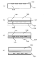
- the thick semiconductor substrate 101 is introduced into the process, and the required semiconductor functional region 103 is formed on the surface 102 of the semiconductor substrate 101.
- a support plate 105 is bonded to the surface 102 of the semiconductor substrate 101 via an adhesive layer 104 and reinforced, and the semiconductor substrate 101 is ground by CMP (chemical mechanical polishing) or the like. Reduce to the design thickness.
- CMP chemical mechanical polishing
- FIG. 5C the required back surface functional layer 107 is formed on the back surface 106 of the thinned semiconductor substrate.
- FIG. 5D a method has been proposed in which the support plate 105 is peeled off to obtain a thin semiconductor substrate 101. During the process, since the semiconductor substrate 101 is reinforced by the support plate 105, mechanical strength and physical strength are high, and handling of the semiconductor substrate is facilitated.
- Patent Document 1 the SiC substrate and the supporting substrate are bonded to each other using wax, adhesive tape, adhesive, etc., and in the heat process after bonding, the thermal load is applied to the adhesive using local annealing such as laser annealing.
- local annealing such as laser annealing.
- Patent Document 2 a step of forming a first buffer film having a surface with a surface roughness R rms of 0.1 to 10000 nm on at least one of the group III nitride semiconductor substrate and the first support substrate. And a method of manufacturing a bonded substrate including the step of bonding the group III nitride semiconductor substrate to the first support substrate via the first buffer film.
- the application layer of the polymer adhesive is exposed to the through portion by penetration etching from the back surface of the Si substrate, and the adhesive is exposed to acid, alkali, gas, plasma, etc. Problem has occurred.
- the present invention has been made in consideration of the above problems, and an object of the present invention is a semiconductor including a step of bonding a support plate to a semiconductor substrate, and a step of separating the bonded support plate from the semiconductor substrate. It is an object of the present invention to provide a method of processing a substrate and a method of manufacturing a semiconductor device using the method.
- the wavelength of the laser beam is substantially set on one main surface of the semiconductor substrate mainly composed of a material that substantially transmits the wavelength of the laser beam.
- a support plate mainly composed of a material to be transmitted through in a vacuum, and a bonding step of pressing and bonding in vacuum with an intermediate layer mainly composed of a material absorbing the laser beam, and the support plate And a separation step of separating the semiconductor substrate and the support plate after the laser light is irradiated from the side to cause the intermediate layer to absorb the laser energy.
- the semiconductor substrate and the support plate can be pressed through the intermediate layer, and the intermediate layer can be joined as the bonding layer.
- the mechanical strength is enhanced, and cracking of the semiconductor substrate can be prevented. This facilitates handling of the semiconductor substrate.
- the bonding portion is irradiated with laser light from the support plate side to cause a large number of cracks in the bonding layer, and the bonding layer is broken to make the support plate unnecessary from the semiconductor substrate. It can be separated. Then, only the intended semiconductor substrate can be obtained, and furthermore, the surface to which the support plate is adhered can be used for other purposes.
- the semiconductor substrate and the support plate are a silicon carbide or gallium nitride semiconductor substrate.
- the bonding step is preferably performed at a pressure of 10 ⁇ 5 Pa or less.
- the bonding step is preferably performed after irradiating the bonding surface of the semiconductor substrate and / or the support plate with an ion beam or an atomic beam.
- the element used for the beam is preferably at least one rare gas selected from helium, neon, argon, krypton, and xenon.
- the bonding property can be enhanced by cleaning the bonding surface and activating the surface atoms.
- the wavelength of the laser light is preferably at least one selected from the wavelengths of 390 nm or more and 1000 nm or less.
- the bonding layer absorb the energy of the laser beam by transmitting the support plate made of silicon carbide.
- a pressing force for bonding the semiconductor substrate and the support plate is preferably 9.8 kPa or more.
- the intermediate layer is an amorphous Si layer stacked on the bonding surfaces of the semiconductor substrate and the support plate.
- the intermediate layer is sequentially stacked on an amorphous Si layer stacked on one of the bonding surfaces of the semiconductor substrate and the support plate, and on the other bonding surface.
- it is an amorphous Si layer, a metal layer, or an amorphous Si layer.
- the intermediate layer is preferably an amorphous Si layer, a metal layer, or an amorphous Si layer sequentially stacked on the bonding surfaces of the semiconductor substrate and the support plate.
- the intermediate layer is an amorphous Si layer and a metal layer sequentially stacked on the bonding surface of the semiconductor substrate and the support plate.
- the high temperature process necessary for device formation can be performed after bonding.
- the thickness of the metal layer constituting the intermediate layer is preferably 2 nm or more and 200 nm or less.
- the energy of the laser beam can be absorbed by the metal layer to protect the underlying semiconductor functional area from being destroyed.
- the total thickness of the amorphous Si layers constituting the intermediate layer is preferably thicker than the thickness of the metal layer.
- the amorphous Si layer and the metal layer react to form the silicide layer, a part of the amorphous Si layer remains, so the bonding layer is surely destroyed by the laser irradiation, and the semiconductor substrate The support plate can be separated.
- the absorption site of the main energy in the intermediate layer by the laser beam is the It is preferable to adjust the focal depth of the laser light so as to be located closer to the support plate than the metal layer.
- the amorphous Si layer located closer to the support plate than the metal layer can be broken efficiently.
- a method of manufacturing a semiconductor device comprises: a first device forming step of forming a semiconductor functional region on one main surface of a semiconductor substrate whose main component is a material that substantially transmits the wavelength of laser light; A support plate whose main component is a material that substantially transmits the wavelength of the laser light is opposed in vacuum to the surface on which the region is formed, and an intermediate layer whose main component is the material that absorbs the laser light is sandwiched.
- the semiconductor substrate and the support plate be a 3C, 4H or 6H polytype silicon carbide semiconductor substrate.
- the 4H or 6H polytype silicon carbide semiconductor substrate having few crystal defects and excellent electrical characteristics can be suitably used for manufacturing a semiconductor device.
- the second device forming step preferably includes a heating step of 600 ° C. or higher.
- the bonding step is a bonding step in which an amorphous Si layer laminated on each bonding surface of the semiconductor substrate and the support plate is an intermediate layer and bonded between the amorphous Si layers. Is preferred.
- an amorphous Si layer, a metal layer, and an amorphous Si layer sequentially stacked on the bonding surfaces of the semiconductor substrate and the support plate are used as intermediate layers. It is preferable that it is a joining process which joins between amorphous Si layers.
- the bonding step is sequentially stacked on an amorphous Si layer stacked on one of the bonding surfaces of the semiconductor substrate and the support plate and on the other bonding surface.
- it is a bonding step in which an amorphous Si layer, a metal layer, and an amorphous Si layer are used as an intermediate layer and bonding is performed between the amorphous Si layers.
- an amorphous Si layer and a metal layer sequentially stacked on the bonding surface of the semiconductor substrate and the support plate are used as an intermediate layer. It is preferable that it is a joining process.
- the high temperature process necessary for device formation can be performed after bonding.
- the surface on which the semiconductor functional region is formed be subjected to planarization treatment after the first device forming step.
- the bonding property is improved because the bonding surface is flat.
- the semiconductor substrate and the support plate can be pressed through the intermediate layer, and the intermediate layer can be joined as the bonding layer.
- the mechanical strength is enhanced, and cracking of the semiconductor substrate can be prevented. This facilitates handling of the semiconductor substrate.
- the bonding portion is irradiated with laser light from the support plate side to cause a large number of cracks in the bonding layer, and the bonding layer is broken to make the support plate unnecessary from the semiconductor substrate. It can be separated. Then, only the intended semiconductor substrate can be obtained, and furthermore, the surface to which the support plate is adhered can be used for other purposes.
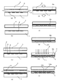
- Example 1 a method of processing a semiconductor substrate according to a first embodiment of the present invention, including a bonding step of bonding the SiC substrate and the support plate, and a separation step of separating the SiC substrate and the support plate
- the method of using the MOSFET to manufacture is described in detail with reference to FIG.
- an n-type 4H—SiC crystal with a diameter of 3 inches, a thickness of 350 ⁇ m, and an impurity concentration of 1 ⁇ 10 18 cm ⁇ 3 (polytype of 4H or 6H is preferable for device manufacture) is used.
- the surface of the SiC substrate 1 is planarized to have a surface roughness Ra ⁇ 0.1 nm by a planarization process such as CMP (chemical mechanical polishing).
- An n-type epitaxial SiC layer (not shown directly but included in the SiC substrate 1) is deposited on the planarized surface of the SiC substrate with an impurity concentration of 1 ⁇ 10 16 cm ⁇ 3 and a thickness of 10 ⁇ m.
- a MOS transistor including a gate electrode, a p-type channel region, an n-type source region, a source contact electrode and the like is formed in the n-type epitaxial SiC layer to form a semiconductor active region 3 (FIG. )).
- a surface protective film that does not deteriorate at 1000 ° C., such as an amorphous Si film, a silicon nitride film, a silicon oxide film, or a silicon oxynitride film can be formed.
- the outermost surface of the surface protective film is easily affected by the surface irregularities of the semiconductor active region 3 and the flatness thereof is reduced. Therefore, the support plate may be subjected to planarization before bonding.
- the main surface 2 on the semiconductor active region 3 side of the SiC substrate 1 on which the MOSFET is formed and the SiC support plate 4 are joined in the following process.
- the main surface 2 on the side of the semiconductor active region 3 of the SiC substrate 1 on which the MOSFET is formed and the main surface of the SiC support plate 4 are arranged to face each other in a vacuum furnace at a vacuum of 10 -6 Pa not shown.
- the surfaces facing each other are irradiated with 200 W of Ar (argon) ion beam 5 and vapor phase etching is performed to clean the bonding surface and to activate the surface atomic layer.
- Ar argon
- the degree of vacuum is not limited to 10 ⁇ 6 Pa, and the bonding surface can be easily activated if it is a high vacuum at a pressure of 10 ⁇ 5 Pa or less.
- the beam irradiated to the bonding surface is not limited to the Ar ion beam 5 but may be an ion beam or an atomic beam. Suitable elements used for the beam include one or more rare gases selected from helium, neon, argon, krypton, and xenon.
- the thickness of the SiC support plate 4 is not particularly limited, but may be, for example, about 500 ⁇ m to 1000 ⁇ m.
- the material of the support plate 4 is preferably the same material as the SiC substrate 1 from the viewpoint of the linear expansion coefficient, but it is particularly limited as long as the linear expansion coefficient is close and a laser beam of a wavelength described later is transmitted.
- the same polytype SiC substrate which is unsuitable for device formation due to excessive dislocation, but is inexpensive and available, another cheap polytype SiC substrate such as 3C, or other similar characteristics. Materials may be used.
- the support plate can also be used again and again.
- an amorphous Si layer 6 is formed to a thickness of 10 nm on each of the ion beam-irradiated surfaces of the SiC substrate 1 and the SiC support plate 4 disposed in the vacuum furnace (FIG. 1 (c)).
- the surface of the amorphous Si layer 6 is vapor-phase etched by irradiation with an Ar ion beam 5 (FIG. 1 (d)).
- the two After activating the surface of the amorphous Si layer 6 by irradiation with the Ar ion beam 5, as shown by the arrows in FIG. 1 (e), the two are immediately pressed in vacuum to form the amorphous Si bonding layer 8a.
- the pressing force in a high vacuum of 10 -5 Pa to 10 -7 Pa is It may be about 9.8 kPa or more. However, in order to prevent unintended separation during the process, in view of safety, the pressing force is preferably about 98 kPa to 980 kPa.
- the main surface 2 on the semiconductor active region 3 side of the SiC substrate 1 on which the MOSFET is formed is opposed to the main surface of the SiC support plate 4 and the Ar ion beam 5 is irradiated thereto. It is not necessary to do this, and it is also possible to activate the surface one by one. In the case of activation one by one, it is necessary to bond the two substrates before the surface after activation is contaminated, but by simultaneously activating the two substrates facing each other, it is possible to immediately after activation. Because there is no concern about surface contamination.
- a back side process is performed as a second device process on the SiC substrate 1 in which the MOSFET to which the SiC support plate 4 is bonded is formed.
- a thickness portion shown by a broken line from the back side of the SiC substrate 1 on which the MOSFET is formed is scraped off by grinding and the like.
- the SiC substrate having a thickness of 350 ⁇ m at the time of introduction is thinned to a thickness of 10 ⁇ m at the time of finishing.
- the polishing by the above-mentioned CMP processing is performed.
- FIG. 1 (g) shows the case where a concave pattern is provided.
- a 50 nm Ni contact electrode layer (not shown) is formed and high temperature annealing at about 1000.degree. Treatment is performed to form a Ni silicide layer.
- a drain electrode film 10 made of a Ti film and a Ni film is stacked on the silicide layer.
- the front surface side of the SiC substrate 1 on which a thin MOSFET with a thickness of 10 ⁇ m is formed is reinforced by the SiC support plate 4, and therefore, substrate cracking and chipping can be prevented (FIG. 1). (G)).
- the SiC support plate 4 is formed on the SiC substrate 1 on which the MOSFET is formed. In the bonded state, a high temperature process at 600 ° C. or higher can be performed.
- the depth of focus is adjusted to the Si bonding layer 8a (intermediate layer 8) and the laser beam 9 is irradiated.
- the laser beam 9 has a wavelength of 532 nm. At this wavelength, the laser beam 9 passes through the SiC support plate and is absorbed by the amorphous Si bonding layer 8a (intermediate layer 8) to generate thermal energy.
- the temperature of the amorphous Si bonding layer 8a (intermediate layer 8) rises rapidly and expands and shrinks, so that the amorphous Si bonding layer 8a (intermediate layer 8) is broken due to a large number of cracks or the like.
- the location of the amorphous Si bonding layer 8 a (intermediate layer 8) destroyed by the irradiation of the laser beam 9 is indicated by the reference numeral 11.
- the laser beam 9 passes through the SiC support plate 4 and has a wavelength sufficiently absorbed by the amorphous Si bonding layer 8a (intermediate layer 8).
- the light transmission wavelength of SiC-4H is about 380 nm or more
- that of SiC-3C is about 556 nm or more
- that of SiC-6H is about 411 nm or more.
- the light transmission wavelength of the Si semiconductor is about 1100 nm or more.
- the wavelength is 1000 nm or more, the absorption edge of the Si film is lowered because it is close to the absorption edge of Si, which is not preferable.
- the wavelength of the laser beam 9 is selected from the range of 380 nm or more and 1000 nm or less. It irradiates, scanning so that it may become a grid
- the shape of the amorphous Si bonding layer 8a (intermediate layer 8) to be broken down by combining the focal depth of the laser beam 9 is spot-like (pulse-like) by the pulse laser beam 9, continuous linear by continuous laser beam, or the like May be formed in combination.
- a wire or a flaky jig (not shown) is inserted between the SiC substrate 1 on which the MOSFET is formed and the SiC support plate 4 to break the amorphous Si junction.
- the layer 8a (intermediate layer 8) is separated into two by applying a peeling stress. Since the amorphous Si bonding layer 8a (intermediate layer 8) is broken by the irradiation of the laser light 9 and many cracks are formed, the bonding strength is significantly reduced. Therefore, by inserting a wire or a thin plate-like jig (not shown) on the side surfaces of both substrates as described above, the bonding layer can be broken at once and separated easily.
- the back surface of the SiC substrate 1 on which the MOSFET is formed is attached to the second support by a known method such as an adhesive.
- the bonding layer residue 12 which is the residue of the amorphous Si bonding layer 8a remaining on the peeling surface of the SiC substrate 1 on which the MOSFET is formed in the previous process and the surface protection film under the amorphous Si bonding layer are removed by a known etchant.
- an electrode and a passivation film are formed on the front surface of the SiC substrate 1 on which the MOSFET attached to the support is formed. From the above, it is possible to obtain the SiC substrate 1 in which a MOSFET having a thickness of 10 ⁇ m and a concave pattern on the back surface is formed.
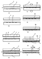
- Example 2 About the processing method of a semiconductor substrate including the joining process of joining a SiC substrate and a support plate concerning Example 2 of the present invention, and the separation process of separating a SiC substrate and a support plate using this processing method The method of manufacturing the MOSFET will be described with reference to FIG.
- the first device process for forming the MOSFET on the SiC substrate 1 is the same as that of the first embodiment (FIG. 1 (b) is shown as FIG. 2 (a)).
- the ion beam 5 is irradiated in vacuum to the opposing surfaces 2 of the SiC substrate 1 on which the MOSFET is formed and the SiC support plate 4, and vapor phase etching is performed to activate the surfaces.
- the ion beam uses a 200 W Ar ion beam.
- an amorphous Si layer 6 (20 nm in thickness) is formed respectively on the surface of the SiC substrate 1 on which the MOSFET is formed and the SiC support plate 4 irradiated with the ion beam 5 (FIG. 2 (b)).
- a metal layer 7 (20 nm thick) such as Ni, and further thereon, an amorphous Si layer 6 (thick 20 nm) to form a film.
- the thickness of the Ni metal layer 7 can be selected from the range of 2 to 200 nm, more preferably from the range of 5 to 100 nm.
- the surface of the opposing amorphous Si layer 6 is vapor-phase etched again using the Ar ion beam 5 (FIG. 2 (d)).
- the surface of the amorphous Si layer 6 is activated by the irradiation of the Ar ion beam 5, as shown in FIG. 2 (e)
- both the SiC substrate 1 on which the MOSFET is formed and the SiC support plate 4 are as shown by arrows.
- the amorphous Si bonding layer 8 a sandwiching the Ni metal layer 7 is formed.
- the thickness of the Ni metal layer 7 is preferably in the range of 2 to 200 nm, more preferably 5 to 100 nm.
- the back surface process (second device process) of the SiC substrate 1 on which the MOSFETs shown in FIGS. 2 (f) to 2 (i) are formed is the same as that of the first embodiment.
- the Ni metal layer 7 is included in the amorphous Si bonding layer 8a unlike the first embodiment. Therefore, depending on the annealing conditions, the Ni metal layer 7 is an amorphous Si layer 6 May form a silicide layer (not shown).
- this silicide layer has a possibility that the destruction of the bonding layer 8 by the laser beam 9 may become unstable for the reason that the composition ratio is not constant in the depth direction, the amorphous Si layer 6 in the bonding layer 8
- the laser light 9 remains without being silicided on the side irradiated with the laser light 9 than the Ni metal layer 7. Therefore, it is desirable that the amorphous Si layer 6 be thicker than the Ni metal layer 7.
- the thickness of the bonded amorphous Si layer 6 is 40 nm in which the thickness on the support side is 20 nm and the total thickness of 20 nm, and the thickness of the amorphous Si layer on the Ni metal layer 7 is 20 nm Therefore, the total thickness is 60 nm, and the thickness of the Ni metal layer 7 is greater than 20 nm.
- the amorphous Si layer 6 becomes thicker than the Ni metal layer 7 on the irradiation surface side of the laser beam 9, so that the rate at which the thermal energy generated by the laser beam 9 is absorbed by the amorphous Si layer 6 is Become more.
- the surface of the SiC substrate 1 having the MOSFET formed over the Ni metal layer 7 is less likely to reach the surface and formed on the surface of the SiC substrate 1 having the MOSFET formed. This is preferable because the adverse effect on the semiconductor functional area 3 being eliminated is eliminated.
- the Ni metal layer 7 is formed on the facing surface on the side of the SiC substrate 1 on which the MOSFET is formed, but may be formed on the facing surface on the side of the SiC support plate 4 .
- Example 3 About the processing method of a semiconductor substrate including the joining process of joining a SiC substrate and a support plate concerning Example 3 of the present invention, and the separation process of separating a SiC substrate and a support plate using this processing method A method of manufacturing the MOSFET will be described with reference to FIG.
- Example 2 not only the amorphous Si layer 6 but also the metal layer 7 (Ni metal layer 7) is included as a layer included in the bonding layer 8a.
- the Ni metal layer 7 is formed on one of the opposing surfaces of the SiC substrate 1 on which the MOSFET is formed and the support plate 4.
- the amorphous Si layer 6 / Ni metal layer 7 is formed on each of the opposing surfaces of the SiC substrate 1 on which the MOSFET is formed and the support plate 4 as shown in FIG.
- This is a manufacturing method in which three layers of the amorphous Si layer 6 are formed. That the bonding is performed between the amorphous Si layers 6 is the same as the first and second embodiments, and the other processes are also the same as the second embodiment.
- the irradiation of the laser light 9 is performed so as to adjust the focal depth to the bonded amorphous Si layer 6.
- the broken amorphous Si layer residue 12b and Ni metal layer residue 12a remain as bonding layer residue 12 in each of the separated SiC substrates, but amorphous Si layer residue 12b Can be removed easily because the Ni metal layer residue 12a thereon is lifted off.
- Example 4 The fourth embodiment of the present invention is basically the same as the third embodiment. The difference from Example 3 is that iron (Fe) is used as the metal film 7 and the film thickness of each of the amorphous Si layer 6 / Fe metal layer 7 / amorphous Si layer 6 is 10 nm / 3 nm / 10 nm. is there.
- the bonding layer residue 12 remains on each of the SiC substrates separated by irradiating the amorphous Si layer 6 so as to adjust the focal depth, but it can be easily removed.
- adhesion to Si is good and mechanical strength may be maintained even in the process at 1000 ° C.
- Various metals other than Ni and Fe can be applied. is there.
- Example 5 About the processing method of a semiconductor substrate including the joining process of joining the SiC substrate and the support plate according to the fifth embodiment of the present invention, and the separation process of separating the SiC substrate and the support plate The method of manufacturing the MOSFET will be described with reference to FIG.
- the fifth embodiment is different from the first to fourth embodiments in that bonding for forming a bonding layer is performed not between amorphous Si layers 6 but between Ni metal layers 7. Therefore, the amorphous Si layer 6 / Ni metal layer 7 is laminated on both the SiC substrate 1 on which the MOSFET is formed, the support plate 4 and the opposite surface. Then, after activating the surface of the Ni metal layer 7 by Ar ion beam 5 irradiation, the SiC substrate 1 on which the MOSFET is formed and the SiC support plate 4 are immediately moved as shown by the arrows, as shown in FIG. By pressing in vacuum, the bonding layer 8 b of the Ni metal layers 7 is formed.
- the Ni metal layer 7 can be broken down and separated by the laser beam 9 irradiation at a lower temperature than the amorphous Si layer 6, the laser beam 9 having energy lower than that of the separation between the amorphous Si layers 6 is sufficient. It is easy.
- the SiC support plate 4 on which the MOSFET is formed is processed to a thickness of 100 ⁇ m or less.
- the high temperature process (up to about 1300 ° C. in the vicinity of the Si melting point) becomes possible in the state where the is stuck.
Landscapes
- Recrystallisation Techniques (AREA)
- Mechanical Treatment Of Semiconductor (AREA)
- Pressure Welding/Diffusion-Bonding (AREA)
Abstract
半導体基板に支持板を接合する工程と、前記接合した支持板を前記半導体基板から分離する工程とを含む半導体基板の処理方法、及び該処理方法を用いる半導体装置の製造方法を提供する。レーザ光の波長を実質的に透過する材料を主成分とする半導体基板1の主面、及び前記レーザ光の波長を実質的に透過する材料を主成分とする支持板4の主面に、前記レーザ光を吸収する材料を主成分とする中間層8をそれぞれ形成し、前記中間層8を形成した半導体基板の主面と前記中間層を形成した支持板とを対向させ、真空中で押圧して接合する接合する。また、前記支持板側から前記レーザ光9を照射し、前記中間層8にレーザエネルギーを吸収させて破壊し、前記半導体基板1と前記支持板4とを分離する分離する。
Description
本発明は、半導体基板に支持板を接合する工程と、前記接合した支持板を前記半導体基板から分離する工程と、を含む半導体基板の処理方法、及び該処理方法を用いる半導体装置の製造方法に関する。
縦型パワーデバイスは、半導体基板に不純物を拡散又は注入して形成された複数の層を備える。これらの層のうち、ドリフト層(キャリアが電界によりドリフト走行する層)は、他の層に比べると電気抵抗が高く、厚くするとオン電圧や順方向電圧降下が顕著に大きくなり、デバイスの定常損失が増加するので好ましくないため、耐圧確保のために必要とされる厚さまで薄くしたいという要求がある。
ドリフト層の厚さを薄くする最も簡単な方法は、薄い半導体基板を使用することである。例えば、定格電圧が600Vの場合、Si基板ならば厚さは100μm程度でよく、SiC基板ならば厚さは10μm程度でよい。そして、フィールドストップ層を備える構造では、空乏層の伸びを抑制するので、半導体基板はさらに薄くすることができる。
ただし、半導体基板の厚さが100μm以下になると、応力によって反り易いという問題や、機械的強度不足から割れたり欠けたりし易いという問題があり、ハンドリングには困難を伴う。特に、SiC基板は、Si基板に比べて硬度は大きいが、弾力性が小さいため、薄くすると割れ易くなり、デバイスの生産効率や良品率を著しく低下させることが懸念されている。
上記の対策として、半導体基板の割れ欠け頻度を少なくするために厚い半導体基板を用いて製造するが、製造終了前に半導体基板を減厚して完成品の半導体基板を薄くする、製造方法が考えられる。
具体的には、図5(a)に示すように、厚い半導体基板101をプロセスに投入し、半導体基板101の表面102に所要の半導体機能領域103を形成する。次いで、図5(b)に示すように、半導体基板101の表面102に接着層104を介して支持板105を接合して補強し、半導体基板101をCMP(化学機械研磨)等により研削して設計厚さまで減厚する。次いで、図5(c)に示すように、減厚した半導体基板の裏面106に所要の裏面機能層107を形成する。最後に、図5(d)に示すように、支持板105を剥がして、薄い半導体基板101を得る方法が提案されている。プロセス中は、支持板105によって半導体基板101が補強されているため、機械的強度、物理的強度が高く、半導体基板のハンドリングが容易になる。
例えば、特許文献1には、ワックス、接着テープ、接着剤等を用いてSiC基板と支持基板とを接着し、接着後の熱工程においてはレーザーアニールなどの局所アニールを用いて接着剤に熱負荷がかからないようにする、SiCデバイスの製造方法が開示されている。
一方、特許文献2には、III族窒化物半導体基板及び第1支持基板のうち少なくとも一方の表面に、表面粗さRrmsが0.1~10000nmの表面を有する第1緩衝膜を形成する工程と、前記第1緩衝膜を介して、前記第1支持基板に前記III族窒化物半導体基板を貼り合わせる工程とを含む、貼り合わせ基板の製造方法が開示されている。
しかしながら、半導体基板と支持基板との接着にワックスや高分子系接着剤等の、耐熱性の低い接着剤を使用すると、製造工程において耐熱温度以上に加熱された場合は、接合部にボイド発生して剥離したり、周囲を汚染したり、接着剤の化学的性質が変化してSi半導体基板と支持板とを分離できなくなる不具合が発生する。このような方法では、半導体基板接着後のプロセスが、接着剤の耐熱温度(100℃~400℃)以下に制限されるという問題がある。
SiC基板を用いる場合は、コンタクト抵抗低減のため1000℃近い高温熱処理を必要とし、SiC基板の熱伝導もよいので、SiC基板接着部の温度を高分子系接着剤の耐熱温度以下に抑えて、熱処理することは容易ではなかった。
また、逆阻止型IGBTを製造する場合は、Si基板裏面からの貫通エッチングによって、高分子系接着剤の塗布層が貫通部に露出し、接着剤が酸、アルカリ、ガス、プラズマ等に曝されて不具合が生じるという問題があった。
本発明は、上記課題を考慮してなされたものであり、本発明の目的は、半導体基板に支持板を接合する工程と、前記接合した支持板を前記半導体基板から分離する工程とを含む半導体基板の処理方法、及び該処理方法を用いる半導体装置の製造方法を提供することにある。
上記目的を達成するため、本発明の半導体基板の処理方法は、レーザ光の波長を実質的に透過する材料を主成分とする半導体基板の一方の主面に、前記レーザ光の波長を実質的に透過する材料を主成分とする支持板を真空中で対向させ、前記レーザ光を吸収する材料を主成分とする中間層を挟んで真空中で押圧しながら接合する接合工程と、前記支持板側から前記レーザ光を照射し、前記中間層にレーザエネルギーを吸収させた後、前記半導体基板と前記支持板とを分離する分離工程と、を含むことを特徴とする。
本発明によれば、半導体基板と支持板とを中間層を介して押圧し、中間層を接合層として接合することができる。半導体基板に支持板を接合すると機械的強度が高まり、半導体基板の割れを防止することができる。これによって、半導体基板の取り扱いが容易になる。また、デバイスを形成した後、上記接合部に支持板側からレーザー光を照射して、前記接合層に多数のクラックを生じせしめ、接合層を破壊して半導体基板から不要となった支持板を分離することができる。そして、目的とする半導体基板だけを得ることができ、更には、支持板を接着していた面を他の目的に使用できる。
本発明の半導体基板の処理方法において、前記半導体基板及び前記支持板が、炭化ケイ素又は窒化ガリウム半導体基板であることが好ましい。
上記態様によれば、レーザ光の波長を実質的に透過する炭化ケイ素や窒化ガリウム半導体基板において好適に用いることができる。
本発明の半導体基板の処理方法において、前記接合工程は、圧力10-5Pa以下の真空度で行われることが好ましい。
上記態様によれば、接合の妨げとなる、接合面の表面酸化を防止することができる。
本発明の半導体基板の処理方法において、前記接合工程は、前記半導体基板、及び/又は、前記支持板の接合面にイオンビーム又は原子ビームを照射してから行われることが好ましい。
また、本発明の半導体基板の処理方法において、前記ビームに用いる元素は、ヘリウム、ネオン、アルゴン、クリプトン、キセノンから選ばれる1種以上の希ガスであることが好ましい。
上記態様によれば、接合面をクリーニングするとともに、表面原子を活性化させて、接合性を高めることができる。
本発明の半導体基板の処理方法において、前記レーザ光の波長は、390nm以上、1000nm以下の波長から選ばれる1種以上であることが好ましい。
上記態様によれば、炭化ケイ素で構成された支持板を透過させて、接合層にレーザ光のエネルギーを吸収させることができる。
本発明の半導体基板の処理方法において、前記半導体基板と前記支持板とを接合する押圧力は、9.8kPa以上であることが好ましい。
上記態様によれば、製造工程における、意図しない半導体基板と支持板との分離を防止することができる。
本発明の半導体基板の処理方法において、前記中間層は、前記半導体基板及び前記支持板のそれぞれの接合面に積層されたアモルファスSi層であることが好ましい。
または、本発明の半導体基板の処理方法において、前記中間層は、前記半導体基板及び前記支持板うち、いずれか一方の接合面に積層されたアモルファスSi層と、もう一方の接合面に順次積層されるアモルファスSi層、金属層、アモルファスSi層であることが好ましい。
または、本発明の半導体基板の処理方法において、前記中間層は、前記半導体基板と前記支持板のそれぞれの接合面に順次積層されたアモルファスSi層、金属層、アモルファスSi層であることが好ましい。
または、本発明の半導体基板の処理方法において、前記中間層は、前記半導体基板と前記支持板のそれぞれの接合面に順次積層されたアモルファスSi層と金属層であることが好ましい。
上記態様によれば、耐熱性の高い中間層材料によって接合できるので、接合した後に、デバイス形成に必要な高温プロセスを実施することができる。
本発明の半導体基板の処理方法において、前記中間層を構成する前記金属層の厚さは、2nm以上、200nm以下であることが好ましい。
上記態様によれば、金属層にレーザ光のエネルギーを吸収させて、その下にある半導体機能領域が破壊されないように防御することができる。
本発明の半導体基板の処理方法において、前記中間層を構成するアモルファスSi層の合計の厚さは、前記金属層の厚さよりも厚いことが好ましい。
上記態様によれば、アモルファスSi層と金属層とが反応してシリサイド層が形成されたとしても、アモルファスSi層が一部残るため、レーザ照射によって確実に接合層を破壊して、半導体基板と支持板を分離することができる。
本発明の半導体基板の処理方法において、前記支持板側から前記レーザ光を照射して前記中間層にレーザエネルギーを吸収させる際に、前記レーザ光による中間層での主たるエネルギーの吸収箇所が、前記金属層よりも支持板側に位置するようにレーザー光の焦点深度を調整することが好ましい。
上記態様によれば、前記金属層よりも支持板側に位置するアモルファスSi層を効率的に破壊することができる。
本発明の半導体装置の製造方法は、レーザ光の波長を実質的に透過する材料を主成分とする半導体基板の一方の主面に半導体機能領域を形成する第一デバイス形成工程と、前記半導体機能領域を形成した面に、前記レーザ光の波長を実質的に透過する材料を主成分とする支持板を真空中で対向させ、前記レーザ光を吸収する材料を主成分とする中間層を挟んで真空中で押圧しながら接合する接合工程と、前記半導体基板の他方の主面を削って減厚する工程と、前記減厚した他方の主面に半導体機能領域を形成する第二デバイス形成工程と、前記支持板側から前記レーザ光を照射し、前記中間層にレーザエネルギーを吸収させた後、前記半導体基板と前記支持板とを分離する分離工程と、を含むことを特徴とする。
上記態様によれば、製造工程における半導体基板の割れを防止することができる。これによって、半導体基板の取り扱いが容易になる。また、接合後にデバイス形成などの高温処理を問題なく行うことができる。
本発明の半導体装置の製造方法において、前記半導体基板及び前記支持板が、3C,4Hまたは6Hのポリタイプの炭化ケイ素半導体基板であることが好ましい。
上記態様によれば、結晶欠陥が少なく、電気特性に優れた4Hまたは6Hのポリタイプの炭化ケイ素半導体基板を半導体装置の製造に好適に用いることができる。
本発明の半導体装置の製造方法において、前記第二デバイス形成工程が、600℃以上の加熱工程を含むことが好ましい。
上記態様によれば、第二デバイス形成工程におけるプロセス上の制約が緩和される。
本発明の半導体装置の製造方法において、前記接合工程は、前記半導体基板及び前記支持板のそれぞれの接合面に積層されたアモルファスSi層を中間層とし、該アモルファスSi層間で接合する接合工程であることが好ましい。
または、本発明の半導体装置の製造方法において、前記接合工程は、前記半導体基板と前記支持板のそれぞれの接合面に順次積層されたアモルファスSi層、金属層、アモルファスSi層を中間層とし、該アモルファスSi層間で接合する接合工程であることが好ましい。
または、本発明の半導体装置の製造方法において、前記接合工程は、前記半導体基板及び前記支持板うち、いずれか一方の接合面に積層されたアモルファスSi層と、もう一方の接合面に順次積層されるアモルファスSi層、金属層、アモルファスSi層を中間層とし、該アモルファスSi層間で接合する接合工程であることが好ましい。
または、本発明の半導体装置の製造方法において、前記接合工程は、前記半導体基板と前記支持板のそれぞれの接合面に順次積層されたアモルファスSi層と金属層を中間層とし、該金属層間で接合する接合工程であることが好ましい。
上記態様によれば、耐熱性の高い中間層材料によって接合できるので、接合した後に、デバイス形成に必要な高温プロセスを実施することができる。
本発明の半導体装置の製造方法において、前記第一デバイス形成工程の後に、前記半導体機能領域を形成した面に平坦化処理を施すことが好ましい。
上記態様によれば、接合面が平坦になるので、接合性がよくなる。
本発明によれば、半導体基板と支持板とを中間層を介して押圧し、中間層を接合層として接合することができる。半導体基板に支持板を接合すると機械的強度が高まり、半導体基板の割れを防止することができる。これによって、半導体基板の取り扱いが容易になる。また、デバイスを形成した後、上記接合部に支持板側からレーザー光を照射して、前記接合層に多数のクラックを生じせしめ、接合層を破壊して半導体基板から不要となった支持板を分離することができる。そして、目的とする半導体基板だけを得ることができ、更には、支持板を接着していた面を他の目的に使用できる。
以下に述べる実施形態の説明および添付図面においては、同様の構成には同一の符号を付し、重複する説明を省略する。また、以下の説明に用いられる添付図面は、見易くまたは理解し易くするために正確なスケール、寸法比で描かれていない。また、本発明はその要旨を超えない限り、以下に説明する実施形態の記載に限定されるものではない。
[実施例1]
以下、本発明の実施例1に係る、SiC基板と支持板とを接合する接合工程、及びSiC基板と支持板とを分離する分離工程を含む、半導体基板の処理方法について、また該処理方法を用いてMOSFETを製造する方法について、図1を参照しながら、詳細に説明する。
以下、本発明の実施例1に係る、SiC基板と支持板とを接合する接合工程、及びSiC基板と支持板とを分離する分離工程を含む、半導体基板の処理方法について、また該処理方法を用いてMOSFETを製造する方法について、図1を参照しながら、詳細に説明する。
SiC基板1としては、直径3インチ、厚さ350μm、不純物濃度1×1018cm-3のn型4H-SiC結晶(デバイス製造には4H又は6Hのポリタイプが好ましい)を用いる。このSiC基板1の表面を、CMP(化学機械的研磨)等の平坦化加工処理によって、表面粗さRa<0.1nmとなるように平坦化する。平坦化したSiC基板の表面に不純物濃度1×1016cm-3、厚さ10μmのn型エピタキシャルSiC層(直接には図示しないが、SiC基板1に含まれる)を堆積する。第一デバイスプロセスでは、前記n型エピタキシャルSiC層に、ゲート電極、p型チャネル領域、n型ソース領域、ソースコンタクト電極等を備えるMOSトランジスタを形成し、半導体能動領域3とする(図1(a))。また、SiC基板1の表面には、必要に応じて、アモルファスSi膜、窒化Si膜、酸化Si膜や酸窒化Si膜等の1000℃では劣化しない表面保護膜を形成することができる。なお、表面保護膜の最表面は、半導体能動領域3の表面凹凸の影響されて平坦度が低下し易いため、支持板を接合する前に、平坦化処理してもよい。
次に、図1(b)に示すように、MOSFETを形成したSiC基板1の半導体能動領域3側の主面2とSiC支持板4を以下のプロセスで接合する。まず、図示しない真空度10-6Paの真空炉中に、MOSFETを形成したSiC基板1の半導体能動領域3側の主面2とSiC支持板4の主面とを対向させるように配置する。対向するそれぞれの面に200WのAr(アルゴン)イオンビーム5を照射し、気相エッチングすることによって、接合する面をクリーンにするとともに、表面原子層を活性化させる。
上記において、真空度は、10-6Paに限定されず、10-5Pa以下の圧力の高真空であれば接合面を容易に活性化することができる。また、接合面に照射するビームは、Arイオンビーム5に限定されず、イオンビーム又は原子ビームであってもよい。ビームに用いる好適な元素としては、ヘリウム、ネオン、アルゴン、クリプトン、キセノンから選ばれる1種以上の希ガスを挙げることができる。また、SiC支持板4の厚さは、特に限定されないが、例えば、500μm~1000μm程度にするとよい。支持板4の材質は、線膨張係数の観点からSiC基板1と同じ材質であることが好ましいが、線膨張係数が近くて、後述する波長のレーザ光を透過させる材料であれば、特に限定されず、例えば、転位過多のためデバイス形成には不適格であるが安価で入手できる同じポリタイプのSiC基板、3C等の安価な他のポリタイプのSiC基板、或いはそれに準ずる特性を備えた他の材料を用いてもよい。なお、支持板は、再度繰り返し使用することもできる。
次に、前記真空炉中に配置された、SiC基板1とSiC支持板4のイオンビーム照射面にアモルファスSi層6をそれぞれ10nmの厚さに成膜し(図1(c))、再び、Arイオンビーム5を照射して、アモルファスSi層6表面を気相エッチングする(図1(d))。Arイオンビーム5の照射によりアモルファスSi層6の表面を活性化させた後、(図1(e))の矢印に示すように、直ちに両者を真空中で押圧することで、アモルファスSi接合層8a(中間層8)を形成し、MOSFETを形成したSiC基板1とSiC支持板4とを接合する(図1(e))。このMOSFETを形成したSiC基板1とSiC支持板4との接合は、接合面の完全さ自体を求めるものではないので、10-5Pa~10-7Paの高真空中での押圧力は、9.8kPa程度以上であればよい。ただし、プロセス中に意図しない分離を防止するため、安全性を考慮して、押圧力は98kPa~980kPa程度が好ましい。
実施例1では、MOSFETを形成したSiC基板1の半導体能動領域3側の主面2とSiC支持板4の主面とを対向させて、それぞれにArイオンビーム5を照射しているが、必ずしもこのようにする必要はなく、1枚ずつその表面を活性化することも可能である。1枚ずつ活性化する場合、活性化後の表面が汚染される前に2枚の基板を接合する必要があるが、2枚の基板を対向させて同時に活性化することで、活性化後すぐに接合できるため、表面汚染の心配がないというメリットがある。
続いて、SiC支持板4が接合されたMOSFETを形成したSiC基板1に、第二デバイスプロセスとして、裏面側プロセスを施す。この裏面側プロセスでは、図1(f)に示すように、MOSFETを形成したSiC基板1の裏面からの破線で示す厚さ部分を研磨研削加工などにより削り落とす。例えば、耐圧600Vクラスのデバイスの場合、投入時に厚さ350μmであったSiC基板を、仕上がり時は厚さ10μmにまで薄くする。さらに研削された面に残る研削ダメージを除去するため、前述のCMP加工による研磨を行なう。
次に、必要に応じて、MOSFETを形成したSiC基板1の裏面にフォトリソグラフィーを用いてレジストパターンを形成し、ドライエッチング処理を行って、スクライブライン上に裏面に深さ10μmの凹パターンを形成する。図1(g)では、凹パターンを設けた場合を示している。その後、MOSFETを形成したSiC基板1の裏面と、この裏面に形成する電極膜10とのコンタクト性を向上させるため、Niコンタクト電極層(図示せず)を50nm形成し、約1000℃の高温アニール処理を行い、Niシリサイド層を形成する。そのシリサイド層上にTi膜およびNi膜からなるドレイン電極膜10を積層する。以上のプロセスによれば、厚さ10μmの薄いMOSFETを形成したSiC基板1のおもて面側がSiC支持板4で補強されているため、基板割れや欠けを防止するすることができる(図1(g))。本発明に係る実施例では、前述のように、SiC支持板4の接合層(中間層8)として主としてアモルファスSi層6を用いているので、MOSFETを形成したSiC基板1にSiC支持板4を接合した状態で、600℃以上の高温プロセスを行うことができる。
続いて、図1(h)に示すように、表面側および裏面側のプロセスが終了したMOSFETを形成したSiC基板1とSiC支持板4との接合基板に対して、SiC支持板4側からアモルファスSi接合層8a(中間層8)に焦点深度をあわせてレーザ光9照射する。レーザ光9は波長532nmのものを用いる。この波長であれば、レーザ光9はSiC支持板を透過し、アモルファスSi接合層8a(中間層8)で吸収され、熱エネルギーを発生させる。その結果、アモルファスSi接合層8a(中間層8)は急激に温度が上昇して膨張収縮することでアモルファスSi接合層8a(中間層8)に多数のクラックが入ることなどにより破壊される。図1(h)ではレーザ光9の照射により破壊されたアモルファスSi接合層8a(中間層8)の箇所を符号11で示す。
レーザ光9はSiC支持板4を透過し、アモルファスSi接合層8a(中間層8)で十分に吸収される波長であればよい。例えば、SiC-4Hの光透過波長はおよそ380nm以上であり、SiC-3Cではおよそ556nm以上であり、SiC-6Hではおよそ411nm以上である。また、Si半導体の光透過波長はおよそ1100nm以上である。ただし、波長1000nm以上ではSiの吸収端に近くなり、Si膜の吸収率が低下してくるため好ましくない。よって、アモルファスSi接合層8aとポリタイプ4HのSiC支持体4を組み合わせにおいて、レーザ光9の波長は、380nm以上、1000nm以下の範囲から選ばれた、波長532nmのレーザ光を基板面に対して格子状のパターンとなるように走査しながら照射する。なお、レーザ光9の焦点深度が合わせられ、破壊されるアモルファスSi接合層8a(中間層8)の形状は、パルスレーザ光9によるスポット状(パルス状)、連続レーザ光による連続線状あるいはそれらを組み合わせとなるように形成してもよい。
続いて、図1(i)示すように、MOSFETを形成したSiC基板1とSiC支持板4との間にワイヤまたは薄片状の治具(図示せず)を挿入し、破壊されたアモルファスSi接合層8a(中間層8)に剥離応力をかけることで2枚に分離する。レーザ光9の照射によりアモルファスSi接合層8a(中間層8)は破壊され、多くのクラックが入っているので、接合強度は著しく低下している。そこで、両基板の側面に、前述のようにワイヤまたは薄片状の治具(図示せず)を挿入することで、接合層が一気に破壊され、容易に分離することができる。また、両基板の接合面の最外周の側面に、予め、剥離起点となるテーパーなどによるV字形凹部を形成しておくことにより、ワイヤまたは薄片状の治具の挿入を容易にして剥離分離することも好ましい。また、MOSFETを形成したSiC基板1より大きいSiC支持板4を用いて、接合界面を明確にすることも好ましい。
次に、MOSFETを形成したSiC基板1の裏面を接着剤などの公知の方法で第2の支持体に貼り付ける。続いて、MOSFETを形成したSiC基板1の前工程の剥離面に残るアモルファスSi接合層8aの残渣である接合層残渣12、およびアモルファスSi接合層下部の表面保護膜を公知のエッチング液で除去する。その後、支持体に貼り付けた状態のMOSFETを形成したSiC基板1のおもて面に電極とパッシベーション膜を形成する。以上により、厚さ10μm、裏面に凹パターンを有するMOSFETを形成したSiC基板1を得ることができる。
[実施例2]
本発明の実施例2に係る、SiC基板と支持板とを接合する接合工程、及びSiC基板と支持板とを分離する分離工程を含む、半導体基板の処理方法について、また該処理方法を用いてMOSFETを製造する方法について、図2を参照しながら説明する。
本発明の実施例2に係る、SiC基板と支持板とを接合する接合工程、及びSiC基板と支持板とを分離する分離工程を含む、半導体基板の処理方法について、また該処理方法を用いてMOSFETを製造する方法について、図2を参照しながら説明する。
実施例2においても、SiC基板1にMOSFETを形成する第一デバイスプロセスは、実施例1と同様である(図1(b)は、図2(a)として示されている)。続いて、MOSFETを形成したSiC基板1とSiC支持板4の対向する表面2に、真空中でイオンビーム5を照射し、気相エッチングして、表面を活性化させる。実施例1と同様に、イオンビームは200WのArイオンビームを用いる。
次に、MOSFETを形成したSiC基板1及びSiC支持板4のイオンビーム5を照射した面に、アモルファスSi層6(厚さ20nm)をそれぞれ成膜し(図2(b))、さらに、図2(c)に示すように、MOSFETを形成したSiC基板1側のアモルファスSi層6上には、例えばNiなどの金属層7(厚さ20nm)、さらにその上に、アモルファスSi層6(厚さ20nm)を成膜して積層する。前記Ni金属層7の厚さは、2~200nmの範囲から、より好ましくは5~100nmの範囲から選択することができる。再びArイオンビーム5を用いて、対向するアモルファスSi層6の表面を気相エッチングする(図2(d))。このArイオンビーム5の照射によりアモルファスSi層6の表面を活性化させた後、図2(e)に示すように直ちにMOSFETを形成したSiC基板1とSiC支持板4の両者を矢印のように、真空中で押圧することで、Ni金属層7を挟んだアモルファスSi接合層8aが形成される。このNi金属層7はレーザ光9を吸収し易いため、後述のレーザ光9照射によるアモルファスSi接合層8aの破壊時に、レーザ光9がMOSFETを形成したSiC基板1の表面に到達して半導体機能領域3を破壊または劣化させる不具合を防止することができる。レーザ光9のエネルギーを十分に吸収するためには、Ni金属層7の厚さは最低でも2nm以上を必要とする。しかし、Ni金属層7の厚さが200nmを超えると、レーザ光9照射によるアモルファスSi層6の破壊が生じにくくなるので好ましくない。従って、前述のように、Ni金属層7の厚さは2~200nm、より好ましくは5~100nmの範囲が好適となる。
続く、図2(f)~(i)に示すMOSFETを形成したSiC基板1の裏面プロセス(第二デバイスプロセス)は、実施例1と同様とする。しかし、実施例2にかかる裏面プロセスでは、実施例1とは異なり、アモルファスSi接合層8aにはNi金属層7が含まれているので、アニール条件によっては、Ni金属層7がアモルファスSi層6と反応してシリサイド層(図示せず)を形成することがある。このシリサイド層はその組成比が深さ方向で一定でないなどの理由のため、レーザ光9による接合層8の破壊が不安定になる可能性があることから、接合層8内のアモルファスSi層6が、Ni金属層7よりもレーザ光9照射面側にシリサイド化されることなく残ることが望ましい。従って、アモルファスSi層6はNi金属層7よりも厚いことが望ましい。実施例2では、接合するアモルファスSi層6の厚さは支持体側が厚さ20nmと20nmを合計した40nm、MOSFETを形成したSiC基板1側はNi金属層7上のアモルファスSi層の厚さ20nmであるので、合わせて60nmとなり、Ni金属層7の厚さ20nmより厚くされている。このような構成とすることにより、アモルファスSi層6がレーザ光9の照射面側でNi金属層7より厚くなるので、レーザ光9により発生する熱エネルギーがアモルファスSi層6に吸収される割合が多くなる。さらにNi金属層7でもレーザ光9エネルギーが吸収されるので、Ni金属層7を超えてMOSFETを形成したSiC基板1の表面に達することが少なくなり、MOSFETを形成したSiC基板1の表面に形成されている半導体機能領域3への悪影響が無くなるので好ましい。
Ni金属層7の残差はアモルファスSi残渣12bを除去することにより、リフトオフされて同時に除去される。以上説明した実施例2では、Ni金属層7はMOSFETを形成したSiC基板1の側の対向面に形成されていたが、SiC支持板4側の対向面に形成される構成とすることもできる。
[実施例3]
本発明の実施例3に係る、SiC基板と支持板とを接合する接合工程、及びSiC基板と支持板とを分離する分離工程を含む、半導体基板の処理方法について、また該処理方法を用いてMOSFETを製造する方法について、図3を参照しながら説明する。
本発明の実施例3に係る、SiC基板と支持板とを接合する接合工程、及びSiC基板と支持板とを分離する分離工程を含む、半導体基板の処理方法について、また該処理方法を用いてMOSFETを製造する方法について、図3を参照しながら説明する。
前述の実施例2では、接合層8aに含まれる層として、アモルファスSi層6だけでなく、金属層7(Ni金属層7)も含まれている。しかし、その製造方法として、実施例2ではMOSFETを形成したSiC基板1と支持板4との対向面のいずれか一方の面にNi金属層7が形成される構成であった。実施例3では、図3に示すように、MOSFETを形成したSiC基板1と支持板4の対向面の両面それぞれに、図3(c)に示すように、アモルファスSi層6/Ni金属層7/アモルファスSi層6の三層が形成される製造方法である。接合がアモルファスSi層6同士の間で行われることは前記実施例1、2と同じであり、それ以外のプロセスについても、実施例2と同様である。
レーザ光9の照射は接合されたアモルファスSi層6に焦点深度を合わせるように照射される。その結果、図3(i)に示すように、分離されたそれぞれのSiC基板には破壊されたアモルファスSi層残渣12bとNi金属層残渣12aが接合層残渣12として残るが、アモルファスSi層残渣12bをSiエッチング液で除去すれば、その上のNi金属層残渣12aはリフトオフされるので、容易に除去することができる。
[実施例4]
本発明の実施例4は、基本的には実施例3と同じである。実施例3との違いは、金属膜7として鉄(Fe)を用いたこと、及びアモルファスSi層6/Fe金属層7/アモルファスSi層6それぞれの膜厚を10nm/3nm/10nmとしたことである。
本発明の実施例4は、基本的には実施例3と同じである。実施例3との違いは、金属膜7として鉄(Fe)を用いたこと、及びアモルファスSi層6/Fe金属層7/アモルファスSi層6それぞれの膜厚を10nm/3nm/10nmとしたことである。
この場合も、アモルファスSi層6に焦点深度を合わせるように照射することで分離されたそれぞれのSiC基板には接合層残渣12が残るが、容易に除去することができる。ここで、金属層7としては、Siに対する密着性が良好であり、かつ1000℃でのプロセスにおいても機械的強度が維持されていればよく、NiやFe以外にもさまざまな金属が適用可能である。
[実施例5]
本発明の実施例5に係る、SiC基板と支持板とを接合する接合工程、及びSiC基板と支持板とを分離する分離工程を含む、半導体基板の処理方法について、また該処理方法を用いてMOSFETを製造する方法について、図4を参照しながら説明する。
本発明の実施例5に係る、SiC基板と支持板とを接合する接合工程、及びSiC基板と支持板とを分離する分離工程を含む、半導体基板の処理方法について、また該処理方法を用いてMOSFETを製造する方法について、図4を参照しながら説明する。
実施例5が前述の実施例1~4と異なる点は、接合層を形成するための接合が、アモルファスSi層6同士の間ではなく、Ni金属層7同士の間で行われることである。そのために、MOSFETを形成したSiC基板1と支持板4と対向面の両面それぞれに、アモルファスSi層6/Ni金属層7が積層される。そして、Arイオンビーム5照射によりNi金属層7表面を活性化させた後、図4(e)に示すように直ちに、MOSFETを形成したSiC基板1とSiC支持板4とを矢印のように、真空中で押圧することで、Ni金属層7同士の接合層8bが形成される。レーザ光9照射により、Ni金属層7を破壊して分離をすることはアモルファスSi層6より低温で可能であるので、アモルファスSi層6間の分離より低エネルギーのレーザ光9の照射でよいため容易である。
以上説明したように、MOSFETを形成したSiC基板1をSiC支持板4を貼りつけて補強することにより、MOSFETを形成したSiC基板1を厚さ100μm以下に薄く加工した状態でも、SiC支持板4を貼りつけた状態で高温プロセス(Si融点近傍の1300℃程度まで)が可能となる。また、高温プロセスの終了後に、SiC支持板4側からのレーザ光9の照射によりMOSFETを形成したSiC基板1とSiC支持板4とを容易に分離することが可能となり、従来のような裏面プロセスにおけるプロセス温度面での制約(400℃以下)が無くなるメリットがある。
1 半導体基板(例えばSiC基板)
2 表面
3 半導体機能領域
4 支持板
5 イオンビーム
6 アモルファスSi層
7 金属層(例えばNi金属層)
8 接合層、中間層
8a アモルファスSi接合層
8b Ni金属接合層
9 レーザ光
10 電極膜
11 破壊箇所
12 接合層残渣
12a Ni金属層残渣
12b アモルファスSi層残渣
2 表面
3 半導体機能領域
4 支持板
5 イオンビーム
6 アモルファスSi層
7 金属層(例えばNi金属層)
8 接合層、中間層
8a アモルファスSi接合層
8b Ni金属接合層
9 レーザ光
10 電極膜
11 破壊箇所
12 接合層残渣
12a Ni金属層残渣
12b アモルファスSi層残渣
Claims (22)
- レーザ光の波長を実質的に透過する材料を主成分とする半導体基板の一方の主面に、前記レーザ光の波長を実質的に透過する材料を主成分とする支持板を真空中で対向させ、前記レーザ光を吸収する材料を主成分とする中間層を挟んで真空中で押圧しながら接合する接合工程と、
前記支持板側から前記レーザ光を照射し、前記中間層にレーザエネルギーを吸収させた後、前記半導体基板と前記支持板とを分離する分離工程と、
を含むことを特徴とする半導体基板の処理方法。 - 前記半導体基板及び前記支持板が、炭化ケイ素又は窒化ガリウム半導体基板である請求項1記載の半導体基板の処理方法。
- 前記接合工程は、圧力10-5Pa以下の真空度で行われる請求項1記載の半導体基板の処理方法。
- 前記接合工程は、前記半導体基板、及び/又は前記支持板の接合面にイオンビーム又は原子ビームを照射してから行われる請求項1記載の半導体基板の処理方法。
- 前記ビームに用いる元素は、ヘリウム、ネオン、アルゴン、クリプトン、キセノンから選ばれる1種以上の希ガスである請求項4記載の半導体基板の処理方法。
- 前記レーザ光の波長は、390nm以上、1000nm以下から選ばれる1種以上である請求項1記載の半導体基板の処理方法。
- 前記半導体基板と前記支持板とを接合する押圧力は、9.8kPa以上である請求項1記載の半導体基板の処理方法。
- 前記中間層は、前記半導体基板及び前記支持板のそれぞれの接合面に積層されたアモルファスSi層である請求項1記載の半導体基板の処理方法。
- 前記中間層は、前記半導体基板及び前記支持板うち、いずれか一方の接合面に積層されたアモルファスSi層と、もう一方の接合面に順次積層されるアモルファスSi層、金属層、アモルファスSi層である請求項1記載の半導体基板の処理方法。
- 前記中間層は、前記半導体基板と前記支持板のそれぞれの接合面に順次積層されたアモルファスSi層、金属層、アモルファスSi層である請求項1記載の半導体基板の処理方法。
- 前記中間層は、前記半導体基板と前記支持板のそれぞれの接合面に順次積層されたアモルファスSi層と金属層である請求項1記載の半導体基板の処理方法。
- 前記中間層を構成する前記金属層の厚さは、2nm以上、200nm以下である請求項9~11のいずれか一項に記載の半導体基板の処理方法。
- 前記中間層を構成するアモルファスSi層の合計の厚さは、前記金属層の厚さよりも厚い請求項9~11のいずれか一項に記載の半導体基板の処理方法。
- 前記支持板側から前記レーザ光を照射して前記中間層にレーザエネルギーを吸収させる際に、前記レーザ光による中間層での主たるエネルギーの吸収箇所が、前記金属層よりも支持板側に位置するようにレーザー光の焦点深度を調整する請求項1記載の半導体基板の処理方法。
- レーザ光の波長を実質的に透過する材料を主成分とする半導体基板の一方の主面に半導体機能領域を形成する第一デバイス形成工程と、
前記半導体機能領域を形成した面に、前記レーザ光の波長を実質的に透過する材料を主成分とする支持板を真空中で対向させ、前記レーザ光を吸収する材料を主成分とする中間層を挟んで真空中で押圧しながら接合する接合工程と、
前記半導体基板の他方の主面を削って減厚する工程と、
前記減厚した他方の主面に半導体機能領域を形成する第二デバイス形成工程と、
前記支持板側から前記レーザ光を照射し、前記中間層にレーザエネルギーを吸収させた後、前記半導体基板と前記支持板とを分離する分離工程と、
を含むことを特徴とする半導体装置の製造方法。 - 前記半導体基板及び前記支持板が、3C、4Hまたは6Hのポリタイプの炭化ケイ素半導体基板である請求項15記載の半導体装置の製造方法。
- 前記第二デバイス形成工程が、600℃以上の加熱工程を含む請求項15記載の半導体装置の製造方法。
- 前記接合工程は、前記半導体基板及び前記支持板のそれぞれの接合面に積層されたアモルファスSi層を中間層とし、該アモルファスSi層間で接合する接合工程である請求項15記載の半導体装置の製造方法。
- 前記接合工程は、前記半導体基板及び前記支持板うち、いずれか一方の接合面に積層されたアモルファスSi層と、もう一方の接合面に順次積層されるアモルファスSi層、金属層、アモルファスSi層を中間層とし、該アモルファスSi層間で接合する接合工程である請求項15記載の半導体装置の製造方法。
- 前記接合工程は、前記半導体基板と前記支持板のそれぞれの接合面に順次積層されたアモルファスSi層、金属層、アモルファスSi層を中間層とし、該アモルファスSi層間で接合する接合工程である請求項15記載の半導体装置の製造方法。
- 前記接合工程は、前記半導体基板と前記支持板のそれぞれの接合面に順次積層されたアモルファスSi層と金属層を中間層とし、該金属層間で接合する接合工程である請求項15記載の半導体装置の製造方法。
- 前記第一デバイス形成工程の後に、前記半導体機能領域を形成した面に平坦化処理を施す請求項15記載の半導体装置の製造方法。
Priority Applications (2)
| Application Number | Priority Date | Filing Date | Title |
|---|---|---|---|
| JP2016512784A JP6210152B2 (ja) | 2014-04-10 | 2015-04-10 | 半導体基板の処理方法及び該処理方法を用いる半導体装置の製造方法 |
| US15/063,976 US9779968B2 (en) | 2014-04-10 | 2016-03-08 | Method for processing semiconductor substrate and method for manufacturing semiconductor device in which said processing method is used |
Applications Claiming Priority (2)
| Application Number | Priority Date | Filing Date | Title |
|---|---|---|---|
| JP2014081035 | 2014-04-10 | ||
| JP2014-081035 | 2014-04-10 |
Related Child Applications (1)
| Application Number | Title | Priority Date | Filing Date |
|---|---|---|---|
| US15/063,976 Continuation US9779968B2 (en) | 2014-04-10 | 2016-03-08 | Method for processing semiconductor substrate and method for manufacturing semiconductor device in which said processing method is used |
Publications (1)
| Publication Number | Publication Date |
|---|---|
| WO2015156381A1 true WO2015156381A1 (ja) | 2015-10-15 |
Family
ID=54287952
Family Applications (1)
| Application Number | Title | Priority Date | Filing Date |
|---|---|---|---|
| PCT/JP2015/061188 Ceased WO2015156381A1 (ja) | 2014-04-10 | 2015-04-10 | 半導体基板の処理方法及び該処理方法を用いる半導体装置の製造方法 |
Country Status (3)
| Country | Link |
|---|---|
| US (1) | US9779968B2 (ja) |
| JP (1) | JP6210152B2 (ja) |
| WO (1) | WO2015156381A1 (ja) |
Cited By (7)
| Publication number | Priority date | Publication date | Assignee | Title |
|---|---|---|---|---|
| JP2017118113A (ja) * | 2015-12-22 | 2017-06-29 | コミサリア ア レネルジー アトミック エ オ ゼネルジー アルテルナティブCommissariat A L’Energie Atomique Et Aux Energies Alternatives | 2つの構造体間の直接接合を実行する方法 |
| JP2020038916A (ja) * | 2018-09-05 | 2020-03-12 | 株式会社Sumco | Soiウェーハ及びその製造方法 |
| KR20210057882A (ko) * | 2019-11-12 | 2021-05-24 | 주식회사 원익아이피에스 | 접착력을 강화시키기 위한 박막 구조체 및 그 제조방법 |
| CN116314035A (zh) * | 2021-12-14 | 2023-06-23 | 铠侠股份有限公司 | 半导体装置、及半导体装置的制造方法 |
| JP2024081936A (ja) * | 2022-12-07 | 2024-06-19 | 信越半導体株式会社 | 半導体基板の製造方法、半導体基板、及び半導体装置 |
| JP2024130242A (ja) * | 2023-03-14 | 2024-09-30 | 三菱電機株式会社 | 半導体装置の製造方法、半導体製造装置及び半導体装置 |
| WO2024202590A1 (ja) * | 2023-03-24 | 2024-10-03 | 信越半導体株式会社 | 半導体基板の製造方法、半導体基板、及び半導体装置 |
Families Citing this family (10)
| Publication number | Priority date | Publication date | Assignee | Title |
|---|---|---|---|---|
| US10964664B2 (en) | 2018-04-20 | 2021-03-30 | Invensas Bonding Technologies, Inc. | DBI to Si bonding for simplified handle wafer |
| JP7135443B2 (ja) * | 2018-05-29 | 2022-09-13 | 富士電機株式会社 | 炭化ケイ素半導体装置及びその製造方法 |
| JP2020102507A (ja) * | 2018-12-21 | 2020-07-02 | 国立大学法人 東京大学 | 分離可能な基板接合体を製造する方法、接合された基板、SiCデバイス及びGaNデバイス |
| JP7293749B2 (ja) * | 2019-03-14 | 2023-06-20 | 富士電機株式会社 | 炭化珪素半導体装置の選別方法 |
| DE102019114140B4 (de) * | 2019-05-27 | 2022-10-20 | Infineon Technologies Ag | Verfahren zum herstellen einer halbleitervorrichtung und halbleiter-wafer |
| US11081393B2 (en) * | 2019-12-09 | 2021-08-03 | Infineon Technologies Ag | Method for splitting semiconductor wafers |
| EP4138116B1 (en) * | 2020-04-13 | 2024-03-13 | Mitsubishi Electric Corporation | Method for manufacturing semiconductor element |
| US12525572B2 (en) | 2021-03-31 | 2026-01-13 | Adeia Semiconductor Bonding Technologies Inc. | Direct bonding and debonding of carrier |
| JP2024515032A (ja) | 2021-03-31 | 2024-04-04 | アデイア セミコンダクター ボンディング テクノロジーズ インコーポレイテッド | 担体の直接接合及び剥離 |
| DE102021110742B4 (de) | 2021-04-27 | 2025-01-16 | Infineon Technologies Ag | Verfahren zum teilen von halbleiterwerkstücken, halbleiterwerkstück und gerät zum definieren eines trennbereichs in halbleiterwerkstücken |
Citations (6)
| Publication number | Priority date | Publication date | Assignee | Title |
|---|---|---|---|---|
| JP2002343972A (ja) * | 2001-05-15 | 2002-11-29 | Sony Corp | 半導体素子の製造方法 |
| JP2004319538A (ja) * | 2003-04-10 | 2004-11-11 | Seiko Epson Corp | 半導体装置の製造方法、集積回路、電子光学装置及び電子機器 |
| JP2008207221A (ja) * | 2007-02-27 | 2008-09-11 | Takehito Shimazu | 常温接合方法 |
| JP2010232625A (ja) * | 2009-03-03 | 2010-10-14 | Sumitomo Electric Ind Ltd | 貼り合わせ基板の製造方法 |
| JP2014011301A (ja) * | 2012-06-29 | 2014-01-20 | Toyota Industries Corp | 半導体装置の製造方法 |
| JP2014056863A (ja) * | 2012-09-11 | 2014-03-27 | Fuji Electric Co Ltd | 半導体装置の製造方法 |
Family Cites Families (13)
| Publication number | Priority date | Publication date | Assignee | Title |
|---|---|---|---|---|
| KR100481994B1 (ko) | 1996-08-27 | 2005-12-01 | 세이코 엡슨 가부시키가이샤 | 박리방법,박막디바이스의전사방법,및그것을이용하여제조되는박막디바이스,박막집적회로장치및액정표시장치 |
| JP4619644B2 (ja) | 1996-08-27 | 2011-01-26 | セイコーエプソン株式会社 | 薄膜素子の転写方法 |
| USRE38466E1 (en) | 1996-11-12 | 2004-03-16 | Seiko Epson Corporation | Manufacturing method of active matrix substrate, active matrix substrate and liquid crystal display device |
| US6586762B2 (en) * | 2000-07-07 | 2003-07-01 | Nichia Corporation | Nitride semiconductor device with improved lifetime and high output power |
| JP2005223165A (ja) * | 2004-02-06 | 2005-08-18 | Sanyo Electric Co Ltd | 窒化物系発光素子 |
| KR20130086057A (ko) | 2005-09-16 | 2013-07-30 | 크리 인코포레이티드 | 실리콘 카바이드 전력 소자들을 그 상에 가지는 반도체 웨이퍼들의 가공방법들 |
| US7989304B2 (en) * | 2006-03-28 | 2011-08-02 | Sharp Kabushiki Kaisha | Method for transferring semiconductor element, method for manufacturing semiconductor device, and semiconductor device |
| US20080164572A1 (en) * | 2006-12-21 | 2008-07-10 | Covalent Materials Corporation | Semiconductor substrate and manufacturing method thereof |
| KR101460086B1 (ko) * | 2009-12-15 | 2014-11-10 | 소이텍 | 기판의 재활용 공정 |
| EP2378549A1 (en) * | 2010-04-06 | 2011-10-19 | S.O.I.Tec Silicon on Insulator Technologies | Method for manufacturing a semiconductor substrate |
| JP5840366B2 (ja) * | 2011-01-06 | 2016-01-06 | 株式会社デンソー | 炭化珪素半導体基板の製造方法および炭化珪素半導体装置の製造方法 |
| JP6322890B2 (ja) * | 2013-02-18 | 2018-05-16 | 住友電気工業株式会社 | Iii族窒化物複合基板およびその製造方法、ならびにiii族窒化物半導体デバイスの製造方法 |
| JP6061251B2 (ja) * | 2013-07-05 | 2017-01-18 | 株式会社豊田自動織機 | 半導体基板の製造方法 |
-
2015
- 2015-04-10 JP JP2016512784A patent/JP6210152B2/ja active Active
- 2015-04-10 WO PCT/JP2015/061188 patent/WO2015156381A1/ja not_active Ceased
-
2016
- 2016-03-08 US US15/063,976 patent/US9779968B2/en active Active
Patent Citations (6)
| Publication number | Priority date | Publication date | Assignee | Title |
|---|---|---|---|---|
| JP2002343972A (ja) * | 2001-05-15 | 2002-11-29 | Sony Corp | 半導体素子の製造方法 |
| JP2004319538A (ja) * | 2003-04-10 | 2004-11-11 | Seiko Epson Corp | 半導体装置の製造方法、集積回路、電子光学装置及び電子機器 |
| JP2008207221A (ja) * | 2007-02-27 | 2008-09-11 | Takehito Shimazu | 常温接合方法 |
| JP2010232625A (ja) * | 2009-03-03 | 2010-10-14 | Sumitomo Electric Ind Ltd | 貼り合わせ基板の製造方法 |
| JP2014011301A (ja) * | 2012-06-29 | 2014-01-20 | Toyota Industries Corp | 半導体装置の製造方法 |
| JP2014056863A (ja) * | 2012-09-11 | 2014-03-27 | Fuji Electric Co Ltd | 半導体装置の製造方法 |
Cited By (14)
| Publication number | Priority date | Publication date | Assignee | Title |
|---|---|---|---|---|
| JP2017118113A (ja) * | 2015-12-22 | 2017-06-29 | コミサリア ア レネルジー アトミック エ オ ゼネルジー アルテルナティブCommissariat A L’Energie Atomique Et Aux Energies Alternatives | 2つの構造体間の直接接合を実行する方法 |
| JP2020038916A (ja) * | 2018-09-05 | 2020-03-12 | 株式会社Sumco | Soiウェーハ及びその製造方法 |
| JP7024668B2 (ja) | 2018-09-05 | 2022-02-24 | 株式会社Sumco | Soiウェーハ及びその製造方法 |
| KR102787577B1 (ko) | 2019-11-12 | 2025-04-02 | 주식회사 원익아이피에스 | 접착력을 강화시키기 위한 박막 구조체 및 그 제조방법 |
| KR20210057882A (ko) * | 2019-11-12 | 2021-05-24 | 주식회사 원익아이피에스 | 접착력을 강화시키기 위한 박막 구조체 및 그 제조방법 |
| CN116314035A (zh) * | 2021-12-14 | 2023-06-23 | 铠侠股份有限公司 | 半导体装置、及半导体装置的制造方法 |
| JP2023087907A (ja) * | 2021-12-14 | 2023-06-26 | キオクシア株式会社 | 半導体装置、及び半導体装置の製造方法 |
| JP7797188B2 (ja) | 2021-12-14 | 2026-01-13 | キオクシア株式会社 | 半導体装置、及び半導体装置の製造方法 |
| JP2024081936A (ja) * | 2022-12-07 | 2024-06-19 | 信越半導体株式会社 | 半導体基板の製造方法、半導体基板、及び半導体装置 |
| JP2024130242A (ja) * | 2023-03-14 | 2024-09-30 | 三菱電機株式会社 | 半導体装置の製造方法、半導体製造装置及び半導体装置 |
| JP7823615B2 (ja) | 2023-03-14 | 2026-03-04 | 三菱電機株式会社 | 半導体装置の製造方法、半導体製造装置及び半導体装置 |
| JP2024137131A (ja) * | 2023-03-24 | 2024-10-07 | 信越半導体株式会社 | 半導体基板の製造方法、半導体基板、及び半導体装置 |
| WO2024202590A1 (ja) * | 2023-03-24 | 2024-10-03 | 信越半導体株式会社 | 半導体基板の製造方法、半導体基板、及び半導体装置 |
| JP7835188B2 (ja) | 2023-03-24 | 2026-03-25 | 信越半導体株式会社 | 半導体基板の製造方法 |
Also Published As
| Publication number | Publication date |
|---|---|
| JP6210152B2 (ja) | 2017-10-11 |
| JPWO2015156381A1 (ja) | 2017-04-13 |
| US20160189982A1 (en) | 2016-06-30 |
| US9779968B2 (en) | 2017-10-03 |
Similar Documents
| Publication | Publication Date | Title |
|---|---|---|
| JP6210152B2 (ja) | 半導体基板の処理方法及び該処理方法を用いる半導体装置の製造方法 | |
| JP5725430B2 (ja) | 固相接合ウエハの支持基板の剥離方法および半導体装置の製造方法 | |
| JP5389627B2 (ja) | ワイドバンドギャップ半導体を積層した複合基板の製造方法 | |
| JP4839818B2 (ja) | 貼り合わせ基板の製造方法 | |
| JP5420968B2 (ja) | 貼り合わせウェーハの製造方法 | |
| JP5967211B2 (ja) | 半導体デバイスの製造方法 | |
| JP5455595B2 (ja) | 貼り合わせウェーハの製造方法 | |
| JP6049571B2 (ja) | 窒化物半導体薄膜を備えた複合基板の製造方法 | |
| KR102658526B1 (ko) | 산화물 단결정 박막을 구비한 복합 웨이퍼의 제조 방법 | |
| JP5065748B2 (ja) | 貼り合わせウエーハの製造方法 | |
| KR102021160B1 (ko) | 투명 soi 웨이퍼의 제조 방법 | |
| TW200425313A (en) | Semiconductor wafer dividing method and apparatus | |
| KR20120095993A (ko) | 응력을 저감한 sos 기판 | |
| TWI567780B (zh) | Method of manufacturing composite wafers | |
| WO2010055857A1 (ja) | Soi基板の作製方法 | |
| JP5336101B2 (ja) | Soi基板の製造方法 | |
| JP2012038932A (ja) | 半導体ウェーハの薄厚化方法および貼り合せウェーハの製造方法 | |
| JP2010278340A (ja) | 貼り合わせウェーハの製造方法 | |
| KR20250162533A (ko) | 반도체 기판의 제조방법, 반도체 기판, 및 반도체 장치 | |
| US11881406B2 (en) | Method of manufacturing a semiconductor device and semiconductor wafer | |
| JP7182105B2 (ja) | Iii族窒化物半導体デバイスの製造方法 | |
| KR20250164724A (ko) | 반도체기판의 제조방법, 반도체기판, 및 반도체장치 | |
| CN117334572A (zh) | 晶圆切割方法 |
Legal Events
| Date | Code | Title | Description |
|---|---|---|---|
| 121 | Ep: the epo has been informed by wipo that ep was designated in this application |
Ref document number: 15777399 Country of ref document: EP Kind code of ref document: A1 |
|
| ENP | Entry into the national phase |
Ref document number: 2016512784 Country of ref document: JP Kind code of ref document: A |
|
| NENP | Non-entry into the national phase |
Ref country code: DE |
|
| 122 | Ep: pct application non-entry in european phase |
Ref document number: 15777399 Country of ref document: EP Kind code of ref document: A1 |