WO2015133290A1 - 半導体装置の製造方法 - Google Patents
半導体装置の製造方法 Download PDFInfo
- Publication number
- WO2015133290A1 WO2015133290A1 PCT/JP2015/054614 JP2015054614W WO2015133290A1 WO 2015133290 A1 WO2015133290 A1 WO 2015133290A1 JP 2015054614 W JP2015054614 W JP 2015054614W WO 2015133290 A1 WO2015133290 A1 WO 2015133290A1
- Authority
- WO
- WIPO (PCT)
- Prior art keywords
- region
- section
- dopant
- semiconductor substrate
- igbt
- Prior art date
- Legal status (The legal status is an assumption and is not a legal conclusion. Google has not performed a legal analysis and makes no representation as to the accuracy of the status listed.)
- Ceased
Links
Images





Classifications
-
- H—ELECTRICITY
- H10—SEMICONDUCTOR DEVICES; ELECTRIC SOLID-STATE DEVICES NOT OTHERWISE PROVIDED FOR
- H10P—GENERIC PROCESSES OR APPARATUS FOR THE MANUFACTURE OR TREATMENT OF DEVICES COVERED BY CLASS H10
- H10P34/00—Irradiation with electromagnetic or particle radiation of wafers, substrates or parts of devices
- H10P34/40—Irradiation with electromagnetic or particle radiation of wafers, substrates or parts of devices with high-energy radiation
- H10P34/42—Irradiation with electromagnetic or particle radiation of wafers, substrates or parts of devices with high-energy radiation with electromagnetic radiation, e.g. laser annealing
-
- H—ELECTRICITY
- H10—SEMICONDUCTOR DEVICES; ELECTRIC SOLID-STATE DEVICES NOT OTHERWISE PROVIDED FOR
- H10D—INORGANIC ELECTRIC SEMICONDUCTOR DEVICES
- H10D12/00—Bipolar devices controlled by the field effect, e.g. insulated-gate bipolar transistors [IGBT]
- H10D12/411—Insulated-gate bipolar transistors [IGBT]
-
- B—PERFORMING OPERATIONS; TRANSPORTING
- B23—MACHINE TOOLS; METAL-WORKING NOT OTHERWISE PROVIDED FOR
- B23K—SOLDERING OR UNSOLDERING; WELDING; CLADDING OR PLATING BY SOLDERING OR WELDING; CUTTING BY APPLYING HEAT LOCALLY, e.g. FLAME CUTTING; WORKING BY LASER BEAM
- B23K26/00—Working by laser beam, e.g. welding, cutting or boring
- B23K26/0006—Working by laser beam, e.g. welding, cutting or boring taking account of the properties of the material involved
-
- B—PERFORMING OPERATIONS; TRANSPORTING
- B23—MACHINE TOOLS; METAL-WORKING NOT OTHERWISE PROVIDED FOR
- B23K—SOLDERING OR UNSOLDERING; WELDING; CLADDING OR PLATING BY SOLDERING OR WELDING; CUTTING BY APPLYING HEAT LOCALLY, e.g. FLAME CUTTING; WORKING BY LASER BEAM
- B23K26/00—Working by laser beam, e.g. welding, cutting or boring
- B23K26/02—Positioning or observing the workpiece, e.g. with respect to the point of impact; Aligning, aiming or focusing the laser beam
- B23K26/06—Shaping the laser beam, e.g. by masks or multi-focusing
- B23K26/0604—Shaping the laser beam, e.g. by masks or multi-focusing by a combination of beams
- B23K26/0608—Shaping the laser beam, e.g. by masks or multi-focusing by a combination of beams in the same heat affected zone [HAZ]
-
- B—PERFORMING OPERATIONS; TRANSPORTING
- B23—MACHINE TOOLS; METAL-WORKING NOT OTHERWISE PROVIDED FOR
- B23K—SOLDERING OR UNSOLDERING; WELDING; CLADDING OR PLATING BY SOLDERING OR WELDING; CUTTING BY APPLYING HEAT LOCALLY, e.g. FLAME CUTTING; WORKING BY LASER BEAM
- B23K26/00—Working by laser beam, e.g. welding, cutting or boring
- B23K26/02—Positioning or observing the workpiece, e.g. with respect to the point of impact; Aligning, aiming or focusing the laser beam
- B23K26/06—Shaping the laser beam, e.g. by masks or multi-focusing
- B23K26/0604—Shaping the laser beam, e.g. by masks or multi-focusing by a combination of beams
- B23K26/0613—Shaping the laser beam, e.g. by masks or multi-focusing by a combination of beams having a common axis
-
- B—PERFORMING OPERATIONS; TRANSPORTING
- B23—MACHINE TOOLS; METAL-WORKING NOT OTHERWISE PROVIDED FOR
- B23K—SOLDERING OR UNSOLDERING; WELDING; CLADDING OR PLATING BY SOLDERING OR WELDING; CUTTING BY APPLYING HEAT LOCALLY, e.g. FLAME CUTTING; WORKING BY LASER BEAM
- B23K26/00—Working by laser beam, e.g. welding, cutting or boring
- B23K26/02—Positioning or observing the workpiece, e.g. with respect to the point of impact; Aligning, aiming or focusing the laser beam
- B23K26/06—Shaping the laser beam, e.g. by masks or multi-focusing
- B23K26/062—Shaping the laser beam, e.g. by masks or multi-focusing by direct control of the laser beam
- B23K26/0622—Shaping the laser beam, e.g. by masks or multi-focusing by direct control of the laser beam by shaping pulses
-
- B—PERFORMING OPERATIONS; TRANSPORTING
- B23—MACHINE TOOLS; METAL-WORKING NOT OTHERWISE PROVIDED FOR
- B23K—SOLDERING OR UNSOLDERING; WELDING; CLADDING OR PLATING BY SOLDERING OR WELDING; CUTTING BY APPLYING HEAT LOCALLY, e.g. FLAME CUTTING; WORKING BY LASER BEAM
- B23K26/00—Working by laser beam, e.g. welding, cutting or boring
- B23K26/08—Devices involving relative movement between laser beam and workpiece
- B23K26/083—Devices involving movement of the workpiece in at least one axial direction
- B23K26/0853—Devices involving movement of the workpiece in at least two axial directions, e.g. in a plane
-
- B—PERFORMING OPERATIONS; TRANSPORTING
- B23—MACHINE TOOLS; METAL-WORKING NOT OTHERWISE PROVIDED FOR
- B23K—SOLDERING OR UNSOLDERING; WELDING; CLADDING OR PLATING BY SOLDERING OR WELDING; CUTTING BY APPLYING HEAT LOCALLY, e.g. FLAME CUTTING; WORKING BY LASER BEAM
- B23K26/00—Working by laser beam, e.g. welding, cutting or boring
- B23K26/352—Working by laser beam, e.g. welding, cutting or boring for surface treatment
- B23K26/354—Working by laser beam, e.g. welding, cutting or boring for surface treatment by melting
-
- H—ELECTRICITY
- H10—SEMICONDUCTOR DEVICES; ELECTRIC SOLID-STATE DEVICES NOT OTHERWISE PROVIDED FOR
- H10D—INORGANIC ELECTRIC SEMICONDUCTOR DEVICES
- H10D12/00—Bipolar devices controlled by the field effect, e.g. insulated-gate bipolar transistors [IGBT]
- H10D12/01—Manufacture or treatment
- H10D12/031—Manufacture or treatment of IGBTs
- H10D12/032—Manufacture or treatment of IGBTs of vertical IGBTs
-
- H—ELECTRICITY
- H10—SEMICONDUCTOR DEVICES; ELECTRIC SOLID-STATE DEVICES NOT OTHERWISE PROVIDED FOR
- H10D—INORGANIC ELECTRIC SEMICONDUCTOR DEVICES
- H10D12/00—Bipolar devices controlled by the field effect, e.g. insulated-gate bipolar transistors [IGBT]
- H10D12/01—Manufacture or treatment
- H10D12/031—Manufacture or treatment of IGBTs
- H10D12/032—Manufacture or treatment of IGBTs of vertical IGBTs
- H10D12/038—Manufacture or treatment of IGBTs of vertical IGBTs having a recessed gate, e.g. trench-gate IGBTs
-
- H—ELECTRICITY
- H10—SEMICONDUCTOR DEVICES; ELECTRIC SOLID-STATE DEVICES NOT OTHERWISE PROVIDED FOR
- H10D—INORGANIC ELECTRIC SEMICONDUCTOR DEVICES
- H10D12/00—Bipolar devices controlled by the field effect, e.g. insulated-gate bipolar transistors [IGBT]
- H10D12/411—Insulated-gate bipolar transistors [IGBT]
- H10D12/441—Vertical IGBTs
- H10D12/461—Vertical IGBTs having non-planar surfaces, e.g. having trenches, recesses or pillars in the surfaces of the emitter, base or collector regions
- H10D12/481—Vertical IGBTs having non-planar surfaces, e.g. having trenches, recesses or pillars in the surfaces of the emitter, base or collector regions having gate structures on slanted surfaces, on vertical surfaces, or in grooves, e.g. trench gate IGBTs
-
- H—ELECTRICITY
- H10—SEMICONDUCTOR DEVICES; ELECTRIC SOLID-STATE DEVICES NOT OTHERWISE PROVIDED FOR
- H10D—INORGANIC ELECTRIC SEMICONDUCTOR DEVICES
- H10D62/00—Semiconductor bodies, or regions thereof, of devices having potential barriers
- H10D62/10—Shapes, relative sizes or dispositions of the regions of the semiconductor bodies; Shapes of the semiconductor bodies
- H10D62/124—Shapes, relative sizes or dispositions of the regions of semiconductor bodies or of junctions between the regions
-
- H—ELECTRICITY
- H10—SEMICONDUCTOR DEVICES; ELECTRIC SOLID-STATE DEVICES NOT OTHERWISE PROVIDED FOR
- H10D—INORGANIC ELECTRIC SEMICONDUCTOR DEVICES
- H10D62/00—Semiconductor bodies, or regions thereof, of devices having potential barriers
- H10D62/10—Shapes, relative sizes or dispositions of the regions of the semiconductor bodies; Shapes of the semiconductor bodies
- H10D62/13—Semiconductor regions connected to electrodes carrying current to be rectified, amplified or switched, e.g. source or drain regions
- H10D62/141—Anode or cathode regions of thyristors; Collector or emitter regions of gated bipolar-mode devices, e.g. of IGBTs
- H10D62/142—Anode regions of thyristors or collector regions of gated bipolar-mode devices
-
- H—ELECTRICITY
- H10—SEMICONDUCTOR DEVICES; ELECTRIC SOLID-STATE DEVICES NOT OTHERWISE PROVIDED FOR
- H10D—INORGANIC ELECTRIC SEMICONDUCTOR DEVICES
- H10D8/00—Diodes
- H10D8/01—Manufacture or treatment
-
- H—ELECTRICITY
- H10—SEMICONDUCTOR DEVICES; ELECTRIC SOLID-STATE DEVICES NOT OTHERWISE PROVIDED FOR
- H10D—INORGANIC ELECTRIC SEMICONDUCTOR DEVICES
- H10D8/00—Diodes
- H10D8/01—Manufacture or treatment
- H10D8/045—Manufacture or treatment of PN junction diodes
-
- H—ELECTRICITY
- H10—SEMICONDUCTOR DEVICES; ELECTRIC SOLID-STATE DEVICES NOT OTHERWISE PROVIDED FOR
- H10D—INORGANIC ELECTRIC SEMICONDUCTOR DEVICES
- H10D84/00—Integrated devices formed in or on semiconductor substrates that comprise only semiconducting layers, e.g. on Si wafers or on GaAs-on-Si wafers
- H10D84/01—Manufacture or treatment
- H10D84/0107—Integrating at least one component covered by H10D12/00 or H10D30/00 with at least one component covered by H10D8/00, H10D10/00 or H10D18/00, e.g. integrating IGFETs with BJTs
- H10D84/0109—Integrating at least one component covered by H10D12/00 or H10D30/00 with at least one component covered by H10D8/00, H10D10/00 or H10D18/00, e.g. integrating IGFETs with BJTs the at least one component covered by H10D12/00 or H10D30/00 being a MOS device
-
- H—ELECTRICITY
- H10—SEMICONDUCTOR DEVICES; ELECTRIC SOLID-STATE DEVICES NOT OTHERWISE PROVIDED FOR
- H10D—INORGANIC ELECTRIC SEMICONDUCTOR DEVICES
- H10D84/00—Integrated devices formed in or on semiconductor substrates that comprise only semiconducting layers, e.g. on Si wafers or on GaAs-on-Si wafers
- H10D84/01—Manufacture or treatment
- H10D84/02—Manufacture or treatment characterised by using material-based technologies
- H10D84/03—Manufacture or treatment characterised by using material-based technologies using Group IV technology, e.g. silicon technology or silicon-carbide [SiC] technology
- H10D84/038—Manufacture or treatment characterised by using material-based technologies using Group IV technology, e.g. silicon technology or silicon-carbide [SiC] technology using silicon technology, e.g. SiGe
-
- H—ELECTRICITY
- H10—SEMICONDUCTOR DEVICES; ELECTRIC SOLID-STATE DEVICES NOT OTHERWISE PROVIDED FOR
- H10D—INORGANIC ELECTRIC SEMICONDUCTOR DEVICES
- H10D84/00—Integrated devices formed in or on semiconductor substrates that comprise only semiconducting layers, e.g. on Si wafers or on GaAs-on-Si wafers
- H10D84/80—Integrated devices formed in or on semiconductor substrates that comprise only semiconducting layers, e.g. on Si wafers or on GaAs-on-Si wafers characterised by the integration of at least one component covered by groups H10D12/00 or H10D30/00, e.g. integration of IGFETs
- H10D84/811—Combinations of field-effect devices and one or more diodes, capacitors or resistors
-
- H—ELECTRICITY
- H10—SEMICONDUCTOR DEVICES; ELECTRIC SOLID-STATE DEVICES NOT OTHERWISE PROVIDED FOR
- H10P—GENERIC PROCESSES OR APPARATUS FOR THE MANUFACTURE OR TREATMENT OF DEVICES COVERED BY CLASS H10
- H10P30/00—Ion implantation into wafers, substrates or parts of devices
- H10P30/20—Ion implantation into wafers, substrates or parts of devices into semiconductor materials, e.g. for doping
- H10P30/202—Ion implantation into wafers, substrates or parts of devices into semiconductor materials, e.g. for doping characterised by the semiconductor materials
- H10P30/204—Ion implantation into wafers, substrates or parts of devices into semiconductor materials, e.g. for doping characterised by the semiconductor materials into Group IV semiconductors
-
- H—ELECTRICITY
- H10—SEMICONDUCTOR DEVICES; ELECTRIC SOLID-STATE DEVICES NOT OTHERWISE PROVIDED FOR
- H10P—GENERIC PROCESSES OR APPARATUS FOR THE MANUFACTURE OR TREATMENT OF DEVICES COVERED BY CLASS H10
- H10P30/00—Ion implantation into wafers, substrates or parts of devices
- H10P30/20—Ion implantation into wafers, substrates or parts of devices into semiconductor materials, e.g. for doping
- H10P30/21—Ion implantation into wafers, substrates or parts of devices into semiconductor materials, e.g. for doping of electrically active species
-
- H—ELECTRICITY
- H10—SEMICONDUCTOR DEVICES; ELECTRIC SOLID-STATE DEVICES NOT OTHERWISE PROVIDED FOR
- H10P—GENERIC PROCESSES OR APPARATUS FOR THE MANUFACTURE OR TREATMENT OF DEVICES COVERED BY CLASS H10
- H10P95/00—Generic processes or apparatus for manufacture or treatments not covered by the other groups of this subclass
- H10P95/90—Thermal treatments, e.g. annealing or sintering
- H10P95/906—Thermal treatments, e.g. annealing or sintering for altering the shape of semiconductors, e.g. smoothing the surface
-
- B—PERFORMING OPERATIONS; TRANSPORTING
- B23—MACHINE TOOLS; METAL-WORKING NOT OTHERWISE PROVIDED FOR
- B23K—SOLDERING OR UNSOLDERING; WELDING; CLADDING OR PLATING BY SOLDERING OR WELDING; CUTTING BY APPLYING HEAT LOCALLY, e.g. FLAME CUTTING; WORKING BY LASER BEAM
- B23K2101/00—Articles made by soldering, welding or cutting
- B23K2101/36—Electric or electronic devices
- B23K2101/40—Semiconductor devices
-
- B—PERFORMING OPERATIONS; TRANSPORTING
- B23—MACHINE TOOLS; METAL-WORKING NOT OTHERWISE PROVIDED FOR
- B23K—SOLDERING OR UNSOLDERING; WELDING; CLADDING OR PLATING BY SOLDERING OR WELDING; CUTTING BY APPLYING HEAT LOCALLY, e.g. FLAME CUTTING; WORKING BY LASER BEAM
- B23K2103/00—Materials to be soldered, welded or cut
- B23K2103/16—Composite materials
- B23K2103/166—Multilayered materials
- B23K2103/172—Multilayered materials wherein at least one of the layers is non-metallic
-
- B—PERFORMING OPERATIONS; TRANSPORTING
- B23—MACHINE TOOLS; METAL-WORKING NOT OTHERWISE PROVIDED FOR
- B23K—SOLDERING OR UNSOLDERING; WELDING; CLADDING OR PLATING BY SOLDERING OR WELDING; CUTTING BY APPLYING HEAT LOCALLY, e.g. FLAME CUTTING; WORKING BY LASER BEAM
- B23K2103/00—Materials to be soldered, welded or cut
- B23K2103/50—Inorganic materials other than metals or composite materials
-
- B—PERFORMING OPERATIONS; TRANSPORTING
- B23—MACHINE TOOLS; METAL-WORKING NOT OTHERWISE PROVIDED FOR
- B23K—SOLDERING OR UNSOLDERING; WELDING; CLADDING OR PLATING BY SOLDERING OR WELDING; CUTTING BY APPLYING HEAT LOCALLY, e.g. FLAME CUTTING; WORKING BY LASER BEAM
- B23K2103/00—Materials to be soldered, welded or cut
- B23K2103/50—Inorganic materials other than metals or composite materials
- B23K2103/52—Ceramics
-
- B—PERFORMING OPERATIONS; TRANSPORTING
- B23—MACHINE TOOLS; METAL-WORKING NOT OTHERWISE PROVIDED FOR
- B23K—SOLDERING OR UNSOLDERING; WELDING; CLADDING OR PLATING BY SOLDERING OR WELDING; CUTTING BY APPLYING HEAT LOCALLY, e.g. FLAME CUTTING; WORKING BY LASER BEAM
- B23K2103/00—Materials to be soldered, welded or cut
- B23K2103/50—Inorganic materials other than metals or composite materials
- B23K2103/56—Inorganic materials other than metals or composite materials being semiconducting
-
- H—ELECTRICITY
- H10—SEMICONDUCTOR DEVICES; ELECTRIC SOLID-STATE DEVICES NOT OTHERWISE PROVIDED FOR
- H10D—INORGANIC ELECTRIC SEMICONDUCTOR DEVICES
- H10D62/00—Semiconductor bodies, or regions thereof, of devices having potential barriers
- H10D62/10—Shapes, relative sizes or dispositions of the regions of the semiconductor bodies; Shapes of the semiconductor bodies
- H10D62/17—Semiconductor regions connected to electrodes not carrying current to be rectified, amplified or switched, e.g. channel regions
- H10D62/393—Body regions of DMOS transistors or IGBTs
-
- H—ELECTRICITY
- H10—SEMICONDUCTOR DEVICES; ELECTRIC SOLID-STATE DEVICES NOT OTHERWISE PROVIDED FOR
- H10D—INORGANIC ELECTRIC SEMICONDUCTOR DEVICES
- H10D8/00—Diodes
Definitions
- the present invention relates to a method of manufacturing a semiconductor device suitable for manufacturing a reverse conducting IGBT (RC-IGBT) in which an insulated gate bipolar transistor (IGBT) and a diode are formed on a single substrate.
- RC-IGBT reverse conducting IGBT
- IGBT insulated gate bipolar transistor
- Patent Document 1 discloses a method of activating a collector region dopant formed on the back surface of an IGBT by laser annealing.
- a first dopant is implanted into a semiconductor substrate, and further, a second dopant is implanted into a region shallower than the implantation depth of the first dopant.
- laser annealing for activating the second dopant in the shallow region is performed using the first pulse laser beam.
- the first dopant in the deep region is not activated.
- laser annealing for activating the first dopant in the deep region is performed using the second pulse laser beam having a long pulse width.
- the lattice defects move from the deep region to the shallow region during the activation annealing of the deep region dopant. For this reason, lattice defects tend to remain in shallow regions. In order to avoid remaining lattice defects, it is desirable to activate the shallow region dopant after activating the deep region dopant. When this method is employed, the lattice defects that have moved to the shallow region during the deep region activation annealing are substantially eliminated during the shallow region activation annealing.
- An IGBT section and a diode section are demarcated on the semiconductor substrate forming the RC-IGBT.
- a collector region and a deeper buffer region are formed in the IGBT section on the back surface of the semiconductor substrate, and a high-concentration n-type cathode region is formed in the diode section.
- the implanted region becomes amorphous.
- the IGBT compartment remains in a crystalline state. That is, before laser annealing, an amorphous region and a crystalline region coexist on the surface of the semiconductor substrate.
- the amorphous region absorbs laser beam energy more easily than the crystalline region and has a lower melting point.
- annealing is performed using a pulsed laser beam that satisfies the conditions necessary for activating the dopant in the deep region in the IGBT section, the surface layer portion of the amorphous region is partially melted (in spots).
- the surface layer part is partially melted and solidified, the surface becomes rough. It is difficult to activate deep region dopants in the IGBT compartment without melting the amorphous region.
- An object of the present invention is to provide a method of manufacturing a semiconductor device including a laser annealing step that can suppress the occurrence of surface roughness and activate a dopant in a deep region.
- a first implantation region by ion-implanting a first dopant of a first conductivity type into a surface layer portion of the IGBT section of the semiconductor substrate having an IGBT section and a diode section defined on the surface;
- a second dopant of a second conductivity type opposite to the first conductivity type is ion-implanted into a region shallower than the first implantation region of the IGBT section of the semiconductor substrate, thereby providing a second Forming an implantation region of
- C A third dopant of the first conductivity type is ion-implanted into the surface layer portion of the diode section of the semiconductor substrate at a higher concentration than the second dopant, thereby amorphizing the implanted region.
- the third implantation region partially melts the IGBT section and the diode section of the semiconductor substrate, and the first implantation is performed. Scanning with a first pulsed laser beam under conditions that activate the first dopant in a region;
- the semiconductor section is scanned by scanning the IGBT section and the diode section of the semiconductor substrate with a second pulse laser beam having a pulse width shorter than that of the first pulse laser beam.
- a first dopant of a first conductivity type is ion-implanted into a surface layer portion of the IGBT section of a semiconductor substrate in which an IGBT section and a diode section are defined on the surface.
- Forming a single implantation region (B) scanning the IGBT section and the diode section of the semiconductor substrate with a first pulsed laser beam under a condition that the surface of the semiconductor substrate does not melt, thereby Activating the dopant; and (C) After the step (b), a second dopant of a second conductivity type opposite to the first conductivity type is formed in a region shallower than the first implantation region of the IGBT section of the semiconductor substrate.
- a third dopant of the first conductivity type is ion-implanted into a surface layer portion of the diode section of the semiconductor substrate at a higher concentration than the second dopant, thereby amorphizing the implanted region.
- the step of activating the second dopant and the third dopant by melting and crystallizing at least the surface layer portion of the second implantation region and the third implantation region of the semiconductor substrate A method for manufacturing a semiconductor device is provided.
- step (d) there is a case where the third injection region is partially melted and the surface of the diode section is roughened by laser annealing using the first pulse laser beam in the step (d).
- step (e) the surface layer of the IGBT section and the diode section is melted by laser annealing using the second pulse laser beam, so that the surface roughness of the diode section is eliminated.
- the diode section is not made amorphous when laser annealing is performed using the first pulse laser beam in the step (b). For this reason, the surface layer portion of the diode section does not melt during laser annealing using the first pulse laser beam. Thereby, surface roughness of the semiconductor substrate can be prevented.
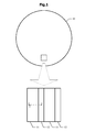
- FIG. 1A and 1B are a plan view and a partially enlarged view of a semiconductor substrate which is a target for laser annealing in a method for manufacturing a semiconductor device according to an embodiment.
- 2 is a cross-sectional view taken along one-dot chain line 2-2 in FIG. 1 in a state where the IGBT and the diode are formed.
- FIG. 3 is a schematic diagram of a laser annealing apparatus used in the semiconductor device manufacturing method according to the embodiment.
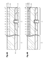
- 4A and 4B are partial cross-sectional views of the semiconductor device in the course of manufacturing the semiconductor device manufacturing method according to the embodiment.
- 4C and 4D are partial cross-sectional views of the semiconductor device in the course of manufacturing the semiconductor device manufacturing method according to the embodiment.
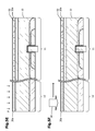
- FIG. 4E and 4F are partial cross-sectional views of the semiconductor device in the course of manufacturing the semiconductor device manufacturing method according to the embodiment.
- FIG. 4G is a partial cross-sectional view of the semiconductor device at an intermediate stage of manufacturing the semiconductor device according to the embodiment.
- 5A and 5B are partial cross-sectional views of a semiconductor device in the course of manufacturing a semiconductor device manufacturing method according to another embodiment.
- 5C and 5D are partial cross-sectional views of the semiconductor device in the course of manufacturing the semiconductor device according to the embodiment shown in FIGS. 5A and 5B.
- 5E and 5F are partial cross-sectional views of the semiconductor device in the course of manufacturing the semiconductor device manufacturing method according to the embodiment shown in FIGS. 5A and 5B.
- FIG. 5G is a partial cross-sectional view of the semiconductor device in the course of manufacturing the semiconductor device manufacturing method according to the embodiment shown in FIGS. 5A and 5B.
- FIG. 1 shows a plan view and a partially enlarged view of a semiconductor substrate 10 to be subjected to laser annealing in a method for manufacturing a semiconductor device according to an embodiment.
- An IGBT section 11 and a diode section 12 are defined on the surface of the semiconductor substrate 10.
- An IGBT is formed in the IGBT section 11 and a diode is formed in the diode section 12.
- FIG. 2 is a cross-sectional view taken along one-dot chain line 2-2 in FIG. 1 in a state where the IGBT and the diode are formed.
- An element structure including a p-type base region 15, an n-type emitter region 16, a gate electrode 17, a gate insulating film 18, and an emitter electrode 19 is formed on the first surface 13 of the semiconductor substrate 10 made of n-type silicon. ing.
- a p-type collector region 20 and an n-type buffer region 21 are formed on the surface layer portion of the second surface 14 opposite to the first surface 13 of the semiconductor substrate 10.
- the buffer region 21 is disposed at a position deeper than the collector region 20.
- a collector electrode 22 is formed on the surface of the collector region 20.
- the depth from the second surface 14 to the interface between the collector region 20 and the buffer region 21 is, for example, in the range of about 0.3 ⁇ m to 0.5 ⁇ m.
- the depth from the second surface 14 to the deepest position of the buffer region 21 is, for example, in the range of 1 ⁇ m to 10 ⁇ m.
- a p-type anode region 25 is formed in the surface layer portion of the first surface 13 of the semiconductor substrate 10.
- An n-type cathode region 26 is formed on the surface layer portion of the second surface 14.
- the anode region 25 has the same depth as the base region 15.
- the cathode region 26 is shallower than the buffer region 21.
- An anode electrode 27 is formed on the first surface 13, and a cathode electrode 28 is formed on the second surface 14.
- FIG. 3 is a schematic diagram of a laser annealing apparatus used in the method for manufacturing a semiconductor device according to the embodiment.
- the laser annealing apparatus includes a first laser light source 41, a second laser light source 31, a propagation optical system 47, a stage 48, and a control device 49.
- the second laser light source 31 includes two solid-state laser oscillators 31A and 31B.
- the solid-state laser oscillators 31A and 31B output a second pulse laser beam having a green wavelength.
- an Nd: YAG laser, an Nd: YLF laser, an Nd: YVO 4 laser, or the like that outputs second-order or higher harmonics is used.
- a laser oscillator that outputs a laser beam having a wavelength in the wavelength range from ultraviolet to green may be used.
- An excimer laser is an example of a laser oscillator that outputs a laser beam in the ultraviolet region.
- a semiconductor laser oscillator is used as the first laser light source 41, and the first laser light source 41 outputs a first pulse laser beam having a wavelength of 808 nm, for example.
- a semiconductor laser oscillator that outputs a first pulse laser beam having a wavelength of 950 nm or less may be used.
- a laser diode array in which a plurality of laser diodes are two-dimensionally arrayed is used as a semiconductor laser oscillator.
- a plurality of laser diodes are monolithically arranged in a one-dimensional array to form a laser bar.
- a two-dimensional laser diode array is formed.
- the direction in which a plurality of laser diodes constituting the laser bar are arranged is called a slow axis.
- the direction in which a plurality of laser bars are stacked is called the fast axis.
- a cylindrical lens is arranged for each laser bar. The cylindrical lens collimates the laser beam output from the laser bar in the fast axis direction or two directions of the fast axis direction and the slow axis direction.
- the first pulse laser beam output from the first laser light source 41 and the second pulse laser beam output from the second laser light source 31 pass through the propagation optical system 47 and are subjected to annealing. 10 is incident.
- the first pulse laser beam output from the first laser light source 41 and the second pulse laser beam output from the second laser light source 31 are incident on the same region on the surface of the semiconductor substrate 10.
- the first pulse laser beam output from the first laser light source 41 is incident on the semiconductor substrate 10 via the attenuator 42, the beam expander 43, the cylindrical lens array group 44, the dichroic mirror 45, and the condenser lens 46. To do.
- the second pulse laser beam output from one solid-state laser oscillator 31A is incident on the beam splitter 35 via the attenuator 32A and the beam expander 33A.
- the second pulse laser beam output from the other solid-state laser oscillator 31B is incident on the beam splitter 35 via the attenuator 32B, the beam expander 33B, and the mirror 34.
- the second pulse laser beams output from the two solid-state laser oscillators 31A and 31B are merged by the beam splitter 35 and propagate along a common path.
- the second pulse laser beam merged into one path by the beam splitter 35 is incident on the semiconductor substrate 10 via the cylindrical lens array group 36, the bending mirror 37, the dichroic mirror 45, and the condenser lens 46.
- the beam expanders 43, 33A, and 33B collimate the incident laser beam and expand the beam diameter.
- the cylindrical lens array groups 44 and 36 and the condenser lens 46 shape the beam cross section on the surface of the semiconductor substrate 10 into a long shape and make the beam profile (light intensity distribution) uniform.
- the first pulse laser beam output from the first laser light source 41 and the second pulse laser beam output from the second laser light source 31 are substantially the same long region on the surface of the semiconductor substrate 10. Is incident on.
- the cylindrical lens array group 44 and the condenser lens 46 function as a homogenizer for the first pulse laser beam output from the first laser light source 41, and the cylindrical lens array group 36 and the condenser lens 46 serve as the second laser light source. It functions as a homogenizer for the second pulse laser beam output from 31.
- the semiconductor substrate 10 is held on the stage 48.
- An XYZ orthogonal coordinate system is defined in which a plane parallel to the surface of the semiconductor substrate 10 is an XY plane, and a normal direction of the surface of the semiconductor substrate 10 is a Z direction.
- the stage 48 moves the semiconductor substrate 10 in the X direction and the Y direction.
- the control device 49 transmits a trigger signal to the solid-state laser oscillators 31A and 31B.
- the solid-state laser oscillators 31 ⁇ / b> A and 31 ⁇ / b> B output the second pulse laser beam in synchronization with the reception of the trigger signal from the control device 49.
- the control device 49 also controls the output timing and pulse width of the first pulse laser beam output from the first laser light source 41.
- FIGS. 4A to 4G a method of manufacturing a semiconductor device according to the embodiment will be described.
- 4A to 4G are partial cross-sectional views of the semiconductor device in the middle of manufacturing.
- an element structure including a base region 15, an emitter region 16, a gate electrode 17, and a gate insulating film 18 is formed on the first surface 13 of the IGBT section 11 of the semiconductor substrate 10.
- An anode region 25 is formed on the first surface 13 of the diode section 12. The dopant in the anode region 25 and the base region 15 is implanted in the same ion implantation process.
- a first implantation region 21a that becomes the buffer region 21 (FIG. 2) is formed.
- lattice defects 50 are formed in the first implantation region 21a.
- boron (B) (second dopant) is ion-implanted into the surface layer portion of the second surface 14 of the IGBT section 11 to form the second collector region 20 (FIG. 2).
- An implantation region 20a is formed.
- the second implantation region 20a is shallower than the first implantation region 21a.
- a lattice defect 50 is also formed in the second implantation region 20a.
- phosphorus (third dopant) is ion-implanted into the surface layer portion of the second surface 14 of the diode section 12, thereby forming a third implantation region 26a that becomes the cathode region 26 (FIG. 2).
- the phosphorus concentration in the third implantation region 26a is higher than the phosphorus concentration in the first implantation region 21a and the boron concentration in the second implantation region 20a.
- the third implantation region 26a becomes amorphous.
- the IGBT section 11 and the diode section 12 of the semiconductor substrate 10 are scanned with the first pulse laser beam 55.
- the first pulse laser beam 55 is output from the first laser light source 41 (FIG. 3).
- the pulse width of the first pulse laser beam 55 is 10 ⁇ s to 20 ⁇ s, and the pulse energy density on the surface of the semiconductor substrate 10 is 4 J / cm 2 to 7 J / cm 2 .
- the overlap rate in the scanning direction is 50% to 75%.
- the overlap ratio is defined as Wo / Wt, where Wt is the width of the beam cross section in the scanning direction, and Wo is the width of the overlapping part of the two shot pulse laser beams adjacent to each other on the time axis. Is done.
- the crystalline IGBT section 11 does not melt, but the third injection region 26a of the amorphous diode section 12 partially melts (in spots).
- FIG. 4E shows a cross-sectional view of the semiconductor substrate 10 after laser annealing with the first pulsed laser beam 55.
- solid phase growth occurs in the first implantation region 21 a and the second implantation region 20 a (FIG. 4B), thereby activating the ion-implanted phosphorus and boron, and the buffer region 21 and the collector region. 20 is formed.
- the lattice defect 50 moves to a shallow region.
- the partially molten third injection region 26a is solidified to roughen the surface. If the annealing conditions are optimized in order to activate the deep buffer region 21, the surface layer portion of the amorphous third implantation region 26a is partially melted. If annealing is performed under conditions that do not melt the third implantation region 26a, it is difficult to sufficiently activate the deep buffer region 21. In other words, in the embodiment, the surface of the diode section 12 is allowed to be roughened by laser annealing for activating the buffer region 21.
- the IGBT section 11 and the diode section 12 of the semiconductor substrate 10 are scanned with the second pulse laser beam 56.
- the second pulse laser beam 56 is output from the second laser light source 31 (FIG. 3).
- Each of the two laser pulses output from the two solid-state laser oscillators 31A and 31B (FIG. 3) has a pulse width of 0.1 ⁇ s to 0.25 ⁇ s, from the incidence of the preceding laser pulse to the incidence of the subsequent laser pulse.
- the delay time is 0.3 ⁇ s to 1 ⁇ s.
- Each pulse energy density of the two laser pulses is 0.8J / cm 2 ⁇ 2.2J / cm 2.
- the overlap rate in the scanning direction is 50% to 80%.
- a method in which two laser pulses are incident on the semiconductor substrate 10 with a slight delay time is employed.
- a method in which one laser pulse is incident can also be employed.
- the shallow collector region 20 and the third implantation region 26a are melted. Under this condition, the deep buffer region 21 of the semiconductor substrate 10 cannot be sufficiently heated, and thus the dopant in the first implantation region 21a (FIG. 4B) cannot be sufficiently activated.
- the dopant in the first implantation region 21a has already been activated by the laser annealing (FIG. 4D) using the first pulsed laser beam 55. Therefore, it is not necessary to activate the dopant in the deep first implantation region 21a (FIG. 4B) by laser annealing using the second pulse laser beam 56 shown in FIG. 4F.
- FIG. 4G shows a cross-sectional view of the semiconductor substrate 10 after laser annealing with the second pulse laser beam 56.
- the third injection region 26a (FIG. 4F) is melted, it is crystallized (solidified), whereby the third dopant is activated and the cathode region 26 is formed.
- the collector region 20 is melted and crystallized, the lattice defects 50 (FIG. 4D) are almost eliminated.
- melting is performed up to the boundary between the amorphous third implantation region 26 a (FIG. 4F) and the single crystal region of the semiconductor substrate 10.
- the crystallinity of the cathode region 26 can be improved and the surface roughness can be eliminated.
- the first dopant in the deep first implantation region 21a can be activated by laser annealing using the first pulse laser beam 55 (FIG. 4D). Furthermore, the surface roughness of the diode section 12 can be eliminated by laser annealing using the second pulse laser beam 56 (FIG. 4F).
- the first pulse laser beam 55 having a relatively long pulse width and a relatively low pulse energy density is suitable for deep region activation annealing.
- the second pulse laser beam 56 having a relatively short pulse width and a relatively high pulse energy density is suitable for activation annealing in a shallow region. Since the second pulse laser beam 56 has a short pulse width, even if the second surface 14 (FIG. 4F) is heated to the melting point or higher, the temperature rise of the first surface 13 can be suppressed. As a result, the surface layer portion of the second surface 14 can be annealed without damaging the IGBT element structure formed on the first surface 13.
- FIGS. 5A to 5G are partial cross-sectional views of the semiconductor device in the middle of manufacturing.
- an IGBT element structure and an anode region 25 are formed on the first surface 13 of the semiconductor substrate 10.
- the first implantation region 21a is formed.
- a lattice defect 50 is formed in the first implantation region 21a.
- the IGBT section 11 and the diode section 12 of the semiconductor substrate 10 are scanned with the first pulse laser beam 55.
- This annealing condition is the same as the annealing condition by the first pulse laser beam 55 shown in FIG. 4D.
- the first dopant in the first implantation region 21a is activated.
- the diode section 12 is not amorphized, the surface layer portion of the diode section 12 does not melt.
- FIG. 5C shows a cross-sectional view of the semiconductor substrate 10 after laser annealing with the first pulsed laser beam 55.
- the buffer region 21 is formed by activating the first dopant in the first implantation region 21a (FIG. 5B).
- the lattice defect 50 moves from a deep region of the buffer region 21 to a shallow region.
- the surface of the diode section 12 is not roughened.
- boron (second dopant) is ion-implanted into the surface layer portion of the IGBT section 11 to form the second implantation region 20a.
- the second implantation region 20 a is shallower than the buffer region 21.
- the lattice defect 50 remains in the second implantation region 20a.
- the third implantation region 26a is formed by ion-implanting phosphorus (third dopant) into the surface layer portion of the diode section 12.
- the third implantation region 26a is in an amorphous state.
- the IGBT section 11 and the diode section 12 of the semiconductor substrate 10 are scanned with the second pulse laser beam 56.
- the annealing conditions are the same as the conditions for laser annealing with the second pulse laser beam 56 shown in FIG. 4F.
- the second implantation region 20a and the third implantation region 26a are melted.
- FIG. 5G shows a cross-sectional view of the semiconductor substrate 10 after laser annealing with the second pulse laser beam 56.
- the third injection region 26a (FIG. 5F) is melted, it is crystallized to activate the third dopant and form the cathode region 26.
- the second implantation region 20a (FIG. 5F) is melted and crystallized, the second dopant is activated and the collector region 20 is formed.
- the lattice defect 50 (FIG. 5F) in the second implantation region 20a is almost eliminated.
- the dopant in the deep first implantation region 21a can be activated by laser annealing using the first pulse laser beam 55 (FIG. 5B). Further, in the laser annealing using the second pulse laser beam 56, the entire surface layer portion of the semiconductor substrate 10 is melted, so that surface roughness due to melting in a patch shape does not occur.
Landscapes
- Physics & Mathematics (AREA)
- Optics & Photonics (AREA)
- Engineering & Computer Science (AREA)
- Plasma & Fusion (AREA)
- Mechanical Engineering (AREA)
- Metal-Oxide And Bipolar Metal-Oxide Semiconductor Integrated Circuits (AREA)
- Electromagnetism (AREA)
- Recrystallisation Techniques (AREA)
Abstract
半導体基板のIGBT区画の表層部に、第1導電型の第1のドーパントを注入して第1の注入領域を形成する。IGBT区画の、第1の注入領域より浅い領域に、第2導電型の第2のドーパントを注入して、第2の注入領域を形成する。ダイオード区画の表層部に、第1導電型の第3のドーパントを、第2のドーパントより高濃度に注入して、アモルファス状態の第3の注入領域を形成する。その後、IGBT区画及びダイオード区画を、第3の注入領域が部分的に溶融し、第1のドーパントが活性化する条件で、レーザアニールを行う。その後、IGBT区画及びダイオード区画を、パルス幅の短いパルスレーザビームでアニールすることにより、IGBT区画及びダイオード区画の全域において、第2の注入領域より浅い表層部を溶融させ、結晶化させる。表面荒れの発生を抑制し、かつ深い領域のドーパントを活性化させることができる。
Description
本発明は、絶縁ゲートバイポーラトランジスタ(IGBT)と、ダイオードとが、1枚の基板に形成された逆導通型IGBT(RC-IGBT)の製造に適した半導体装置の製造方法に関する。
下記の特許文献1に、IGBTの背面に形成されるコレクタ領域のドーパントを、レーザアニールにより活性化させる方法が開示されている。このレーザアニール方法では、まず、半導体基板に第1のドーパントを注入し、さらに、第1のドーパントの注入深さより浅い領域に、第2のドーパントを注入する。
その後、第1のパルスレーザビームを用いて、浅い領域の第2のドーパントを活性化するためのレーザアニールを行う。このレーザアニールでは、深い領域の第1のドーパントは活性化されない。さらに、パルス幅の長い第2のパルスレーザビームを用いて、深い領域の第1のドーパントを活性化させるためのレーザアニールを行う。
浅い領域のドーパントを活性化させた後、深い領域のドーパントを活性化させる方法の場合、深い領域のドーパントの活性化アニール時に、格子欠陥が深い領域から浅い領域に向かって移動する。このため、浅い領域に格子欠陥が残存し易い。格子欠陥の残存を回避するために、深い領域のドーパントを活性化させた後に、浅い領域のドーパントを活性化させることが望ましい。この方法を採用すると、深い領域の活性化アニール中に浅い領域に移動した格子欠陥が、浅い領域の活性化アニール中にほぼ消滅する。
RC-IGBTを形成する半導体基板には、IGBT区画とダイオード区画とが画定されている。半導体基板の背面のIGBT区画に、コレクタ領域と、それよりも深いバッファ領域とが形成され、ダイオード区画に、高濃度のn型カソード領域が形成される。高濃度のn型カソード領域を形成するために、リンをイオン注入すると、注入された領域がアモルファス状態になる。これに対し、IGBT区画は結晶状態のままである。すなわち、レーザアニール前は、半導体基板の表面に、アモルファス状態の領域と、結晶状態の領域が混在する。
アモルファス領域は、結晶領域よりもレーザビームのエネルギを吸収しやすいうえに、融点が低い。IGBT区画内の深い領域のドーパントを活性化させるのに必要な条件を満たすパルスレーザビームを用いてアニールを行うと、アモルファス領域の表層部が部分的に(斑状に)溶融する。表層部が部分的に溶融して固化すると、表面が荒れてしまう。アモルファス領域を溶融させることなく、IGBT区画内の深い領域のドーパントを活性化することは困難である。
本発明の目的は、表面荒れの発生を抑制し、かつ深い領域のドーパントを活性化させることができるレーザアニール工程を含む半導体装置の製造方法を提供することである。
本発明の第1の観点によると、
(a)表面にIGBT区画とダイオード区画とが画定された半導体基板の前記IGBT区画の表層部に、第1導電型の第1のドーパントをイオン注入して第1の注入領域を形成する工程と、
(b)前記半導体基板の前記IGBT区画の、前記第1の注入領域より浅い領域に、前記第1導電型とは反対の第2導電型の第2のドーパントをイオン注入することにより、第2の注入領域を形成する工程と、
(c)前記半導体基板の前記ダイオード区画の表層部に、前記第1導電型の第3のドーパントを、前記第2のドーパントより高濃度にイオン注入することにより、注入された領域をアモルファス化して第3の注入領域を形成する工程と、
(d)前記工程(a)、(b)及び(c)の後に、前記半導体基板の前記IGBT区画及び前記ダイオード区画を、前記第3の注入領域が部分的に溶融し、前記第1の注入領域の前記第1のドーパントが活性化する条件で、第1のパルスレーザビームで走査する工程と、
(e)前記工程(d)の後に、前記半導体基板の前記IGBT区画及び前記ダイオード区画を、前記第1のパルスレーザビームよりパルス幅の短い第2のパルスレーザビームで走査することにより、前記半導体基板の前記IGBT区画及び前記ダイオード区画の全域において、前記第2の注入領域より浅い表層部を溶融させ、結晶化させる工程と
を有する半導体装置の製造方法が提供される。
(a)表面にIGBT区画とダイオード区画とが画定された半導体基板の前記IGBT区画の表層部に、第1導電型の第1のドーパントをイオン注入して第1の注入領域を形成する工程と、
(b)前記半導体基板の前記IGBT区画の、前記第1の注入領域より浅い領域に、前記第1導電型とは反対の第2導電型の第2のドーパントをイオン注入することにより、第2の注入領域を形成する工程と、
(c)前記半導体基板の前記ダイオード区画の表層部に、前記第1導電型の第3のドーパントを、前記第2のドーパントより高濃度にイオン注入することにより、注入された領域をアモルファス化して第3の注入領域を形成する工程と、
(d)前記工程(a)、(b)及び(c)の後に、前記半導体基板の前記IGBT区画及び前記ダイオード区画を、前記第3の注入領域が部分的に溶融し、前記第1の注入領域の前記第1のドーパントが活性化する条件で、第1のパルスレーザビームで走査する工程と、
(e)前記工程(d)の後に、前記半導体基板の前記IGBT区画及び前記ダイオード区画を、前記第1のパルスレーザビームよりパルス幅の短い第2のパルスレーザビームで走査することにより、前記半導体基板の前記IGBT区画及び前記ダイオード区画の全域において、前記第2の注入領域より浅い表層部を溶融させ、結晶化させる工程と
を有する半導体装置の製造方法が提供される。
本発明の第2の観点によると
(a)表面にIGBT区画とダイオード区画とが画定された半導体基板の前記IGBT区画の表層部に、第1導電型の第1のドーパントをイオン注入して第1の注入領域を形成する工程と、
(b)前記半導体基板の前記IGBT区画及び前記ダイオード区画を、前記半導体基板の表面が溶融しない条件で、第1のパルスレーザビームで走査することにより、前記第1の注入領域の前記第1のドーパントを活性化させる工程と、
(c)前記工程(b)の後に、前記半導体基板の前記IGBT区画の、前記第1の注入領域より浅い領域に、前記第1導電型とは反対の第2導電型の第2のドーパントをイオン注入することにより、第2の注入領域を形成する工程と、
(d)前記半導体基板の前記ダイオード区画の表層部に、前記第1導電型の第3のドーパントを、前記第2のドーパントより高濃度にイオン注入することにより、注入された領域をアモルファス化して第3の注入領域を形成する工程と、
(e)前記工程(c)及び(d)の後に、前記半導体基板の前記IGBT区画及び前記ダイオード区画を、前記第1のパルスレーザビームよりパルス幅の短い第2のパルスレーザビームで走査することにより、前記半導体基板の前記第2の注入領域及び前記第3の注入領域の少なくとも表層部を溶融させて、結晶化させることにより、前記第2のドーパント及び前記第3のドーパントを活性化させる工程と
を有する半導体装置の製造方法が提供される。
(a)表面にIGBT区画とダイオード区画とが画定された半導体基板の前記IGBT区画の表層部に、第1導電型の第1のドーパントをイオン注入して第1の注入領域を形成する工程と、
(b)前記半導体基板の前記IGBT区画及び前記ダイオード区画を、前記半導体基板の表面が溶融しない条件で、第1のパルスレーザビームで走査することにより、前記第1の注入領域の前記第1のドーパントを活性化させる工程と、
(c)前記工程(b)の後に、前記半導体基板の前記IGBT区画の、前記第1の注入領域より浅い領域に、前記第1導電型とは反対の第2導電型の第2のドーパントをイオン注入することにより、第2の注入領域を形成する工程と、
(d)前記半導体基板の前記ダイオード区画の表層部に、前記第1導電型の第3のドーパントを、前記第2のドーパントより高濃度にイオン注入することにより、注入された領域をアモルファス化して第3の注入領域を形成する工程と、
(e)前記工程(c)及び(d)の後に、前記半導体基板の前記IGBT区画及び前記ダイオード区画を、前記第1のパルスレーザビームよりパルス幅の短い第2のパルスレーザビームで走査することにより、前記半導体基板の前記第2の注入領域及び前記第3の注入領域の少なくとも表層部を溶融させて、結晶化させることにより、前記第2のドーパント及び前記第3のドーパントを活性化させる工程と
を有する半導体装置の製造方法が提供される。
第1の観点による方法では、工程(d)における第1のパルスレーザビームを用いたレーザアニールにより、第3の注入領域が部分的に溶融し、ダイオード区画の表面が荒れる場合がある。工程(e)において、第2のパルスレーザビームを用いたレーザアニールにより、IGBT区画及びダイオード区画の全域において表層部を溶融させるため、ダイオード区画の表面荒れが解消する。
第2の観点による方法では、工程(b)において第1のパルスレーザビームを用いてレーザアニールを行うときに、ダイオード区画がアモルファス化されていない。このため、第1のパルスレーザビームを用いたレーザアニール時に、ダイオード区画の表層部が溶融しない。これにより、半導体基板の表面荒れを防止することができる。
図1に、実施例による半導体装置の製造方法でレーザアニール対象となる半導体基板10の平面図、及び部分拡大図を示す。半導体基板10の表面に、IGBT区画11及びダイオード区画12が画定されている。IGBT区画11にIGBTが形成され、ダイオード区画12にダイオードが形成される。
図2に、IGBT及びダイオードが形成された状態の図1の一点鎖線2-2における断面図を示す。
IGBT区画11の構成について説明する。n型のシリコンからなる半導体基板10の第1の面13に、p型のベース領域15、n型のエミッタ領域16、ゲート電極17、ゲート絶縁膜18、エミッタ電極19を含む素子構造が形成されている。半導体基板10の、第1の面13とは反対側の第2の面14の表層部に、p型のコレクタ領域20及びn型のバッファ領域21が形成されている。バッファ領域21は、コレクタ領域20よりも深い位置に配置される。コレクタ領域20の表面にコレクタ電極22が形成されている。半導体基板10として、通常はシリコン単結晶基板が用いられる。ゲート-エミッタ間の電圧で、電流のオンオフ制御を行うことができる。
第2の面14からコレクタ領域20とバッファ領域21との界面までの深さは、例えば約0.3μm~0.5μmの範囲内である。第2の面14からバッファ領域21の最も深い位置までの深さは、例えば1μm~10μmの範囲内である。
次に、ダイオード区画12の構成について説明する。半導体基板10の第1の面13の表層部に、p型のアノード領域25が形成されている。第2の面14の表層部に、n型のカソード領域26が形成されている。アノード領域25は、ベース領域15と同一の深さを有する。カソード領域26は、バッファ領域21より浅い。第1の面13にアノード電極27が形成され、第2の面14にカソード電極28が形成されている。
図3に、実施例による半導体装置の製造方法で用いられるレーザアニール装置の概略図を示す。このレーザアニール装置は、第1のレーザ光源41、第2のレーザ光源31、伝搬光学系47、ステージ48、及び制御装置49を含む。第2のレーザ光源31は、2台の固体レーザ発振器31A、31Bを含む。固体レーザ発振器31A、31Bは、緑色域の波長を有する第2のパルスレーザビームを出力する。固体レーザ発振器31A、31Bには、例えば2次以上の高調波を出力するNd:YAGレーザ、Nd:YLFレーザ、Nd:YVO4レーザ等が用いられる。なお、固体レーザ発振器31A、31Bに代えて、紫外から緑色までの波長域の波長を有するレーザビームを出力するレーザ発振器を用いてもよい。紫外域のレーザビームを出力するレーザ発振器として、エキシマレーザが挙げられる。第1のレーザ光源41には、例えば半導体レーザ発振器が用いられ、第1のレーザ光源41は、例えば波長808nmの第1のパルスレーザビームを出力する。なお、波長950nm以下の第1のパルスレーザビームを出力する半導体レーザ発振器を用いてもよい。
半導体レーザ発振器として、複数のレーザダイオードを二次元にアレイ化したレーザダイオードアレイが用いられる。以下、レーザダイオードアレイの構造について説明する。複数のレーザダイオードがモノリシックに一次元アレイ化されてレーザバーが構成される。複数のレーザバーを積み重ねることにより、二次元アレイ化したレーザダイオードアレイが構成される。レーザバーを構成する複数のレーザダイオードが配列する方向を遅軸という。複数のレーザバーが積み重ねられた方向を速軸という。レーザバーごとにシリンドリカルレンズが配置されている。シリンドリカルレンズは、レーザバーから出力されたレーザビームを、速軸方向、または速軸方向と遅軸方向との2方向に関してコリメートする。
第1のレーザ光源41から出力された第1のパルスレーザビーム、及び第2のレーザ光源31から出力された第2のパルスレーザビームが、伝搬光学系47を経由して、アニール対象の半導体基板10に入射する。第1のレーザ光源41から出力された第1のパルスレーザビームと、第2のレーザ光源31から出力された第2のパルスレーザビームとは、半導体基板10の表面の同一の領域に入射する。
次に、伝搬光学系47の構成及び作用について説明する。第1のレーザ光源41から出力された第1のパルスレーザビームが、アッテネータ42、ビームエキスパンダ43、シリンドリカルレンズアレイ群44、ダイクロイックミラー45、及びコンデンサレンズ46を経由して、半導体基板10に入射する。
一方の固体レーザ発振器31Aから出力された第2のパルスレーザビームが、アッテネータ32A及びビームエキスパンダ33Aを経由して、ビームスプリッタ35に入射する。他方の固体レーザ発振器31Bから出力された第2のパルスレーザビームが、アッテネータ32B及びビームエキスパンダ33B、ミラー34を経由して、ビームスプリッタ35に入射する。2つの固体レーザ発振器31A、31Bから出力された第2のパルスレーザビームが、ビームスプリッタ35で合流し、共通の経路に沿って伝搬する。
ビームスプリッタ35で1本の経路に合流した第2のパルスレーザビームは、シリンドリカルレンズアレイ群36、ベンディングミラー37、ダイクロイックミラー45、及びコンデンサレンズ46を経由して、半導体基板10に入射する。
ビームエキスパンダ43、33A、33Bは、入射したレーザビームをコリメートするとともに、ビーム径を拡大する。シリンドリカルレンズアレイ群44、36及びコンデンサレンズ46は、半導体基板10の表面におけるビーム断面を長尺形状に整形するとともに、ビームプロファイル(光強度分布)を均一化する。第1のレーザ光源41から出力された第1のパルスレーザビームと、第2のレーザ光源31から出力された第2のパルスレーザビームとは、半導体基板10の表面において、ほぼ同一の長尺領域に入射する。シリンドリカルレンズアレイ群44及びコンデンサレンズ46が、第1のレーザ光源41から出力された第1のパルスレーザビーム用のホモジナイザとして機能し、シリンドリカルレンズアレイ群36及びコンデンサレンズ46が、第2のレーザ光源31から出力された第2のパルスレーザビーム用のホモジナイザとして機能する。
半導体基板10は、ステージ48に保持されている。半導体基板10の表面に平行な面をXY面とし、半導体基板10の表面の法線方向をZ方向とするXYZ直交座標系を定義する。ステージ48は、制御装置49からの制御を受けて、半導体基板10をX方向及びY方向に移動させる。制御装置49が、固体レーザ発振器31A、31Bにトリガ信号を送信する。固体レーザ発振器31A、31Bは、制御装置49からのトリガ信号の受信に同期して、第2のパルスレーザビームを出力する。また、制御装置49は、第1のレーザ光源41から出力される第1のパルスレーザビームの出力タイミング、及びパルス幅を制御する。
図4A~図4Gを参照して、実施例による半導体装置の製造方法について説明する。図4A~図4Gは、製造途中段階における半導体装置の部分断面図を示している。
図4Aに示すように、半導体基板10のIGBT区画11の第1の面13に、ベース領域15、エミッタ領域16、ゲート電極17、及びゲート絶縁膜18を含む素子構造が形成されている。ダイオード区画12の第1の面13に、アノード領域25が形成されている。アノード領域25及びベース領域15のドーパントは、同一のイオン注入工程で注入される。
IGBT区画11の第2の面14の表層部に、リン(P)(第1のドーパント)をイオン注入することにより、バッファ領域21(図2)となる第1の注入領域21aを形成する。イオン注入により、第1の注入領域21a内に格子欠陥50が形成される。
図4Bに示すように、IGBT区画11の第2の面14の表層部に、ボロン(B)(第2のドーパント)をイオン注入することにより、コレクタ領域20(図2)となる第2の注入領域20aを形成する。第2の注入領域20aは、第1の注入領域21aよりも浅い。第2の注入領域20a内にも格子欠陥50が形成される。
図4Cに示すように、ダイオード区画12の第2の面14の表層部にリン(第3のドーパント)をイオン注入することにより、カソード領域26(図2)となる第3の注入領域26aを形成する。第3の注入領域26aのリン濃度は、第1の注入領域21aのリン濃度及び第2の注入領域20aのボロン濃度より高い。ボロンよりも重いリンを、高濃度に注入することにより、第3の注入領域26aはアモルファス状態になる。
図4Dに示すように、半導体基板10のIGBT区画11及びダイオード区画12を、第1のパルスレーザビーム55で走査する。第1のパルスレーザビーム55は、第1のレーザ光源41(図3)から出力されたものである。第1のパルスレーザビーム55のパルス幅は10μs~20μsであり、半導体基板10の表面におけるパルスエネルギ密度は4J/cm2~7J/cm2である。走査方向に関するオーバラップ率は、50%~75%である。走査方向に関するビーム断面の幅をWtで表し、時間軸上で相互に隣り合う2ショットのパルスレーザビームのビーム断面が重なる部分の幅をWoで表したとき、オーバラップ率はWo/Wtで定義される。
上述のレーザアニール条件では、結晶状態のIGBT区画11は溶融しないが、アモルファス状態のダイオード区画12の第3の注入領域26aは、部分的に(斑状に)溶融する。
図4Eに、第1のパルスレーザビーム55でレーザアニールを行った後の半導体基板10の断面図を示す。IGBT区画11においては、第1の注入領域21a及び第2の注入領域20a(図4B)で固相成長が生じることにより、イオン注入されたリン及びボロンが活性化され、バッファ領域21及びコレクタ領域20が形成される。このとき、格子欠陥50が浅い領域に移動する。
ダイオード区画12においては、部分的に溶融した第3の注入領域26aが固化することにより、その表面が荒れる。深いバッファ領域21の活性化を行うためにアニール条件を最適化すると、アモルファス状態の第3の注入領域26aの表層部が部分的に溶融してしまう。第3の注入領域26aを溶融させない条件でアニールを行うと、深いバッファ領域21の十分な活性化を行うことが困難である。言い換えると、実施例では、バッファ領域21の活性化のためのレーザアニールによって、ダイオード区画12の表面に荒れが発生することを許容している。
図4Fに示すように、半導体基板10のIGBT区画11及びダイオード区画12を、第2のパルスレーザビーム56で走査する。第2のパルスレーザビーム56は、第2のレーザ光源31(図3)から出力されたものである。2つの固体レーザ発振器31A、31B(図3)から出力される2つのレーザパルスの各々のパルス幅は0.1μs~0.25μsであり、先行するレーザパルスの入射から後続のレーザパルスの入射までの遅延時間は0.3μs~1μsである。2つのレーザパルスの各々のパルスエネルギ密度は、0.8J/cm2~2.2J/cm2である。走査方向に関するオーバラップ率は50%~80%である。なお、本実施例では、2つのレーザパルスを、わずかの遅延時間で半導体基板10に入射させる方法を採用したが、1つのレーザパルスを入射させる方法を採用することも可能である。
上述のレーザアニール条件では、浅いコレクタ領域20及び第3の注入領域26aが溶融する。なお、この条件では、半導体基板10の深いバッファ領域21まで十分加熱することができないため、第1の注入領域21a(図4B)内のドーパントを十分活性化させることはできない。実施例においては、第1のパルスレーザビーム55によるレーザアニール(図4D)で、第1の注入領域21a内のドーパントが既に活性化されている。従って、図4Fに示した第2のパルスレーザビーム56を用いたレーザアニールで、深い第1の注入領域21a(図4B)内のドーパントを活性化させる必要はない。
図4Gに、第2のパルスレーザビーム56でレーザアニールを行った後の半導体基板10の断面図を示す。第3の注入領域26a(図4F)が溶融した後、結晶化(固化)することにより、第3のドーパントが活性化し、カソード領域26が形成される。さらに、コレクタ領域20が溶融した後、結晶化することにより、格子欠陥50(図4D)がほぼ消滅する。
第2のパルスレーザビーム56によるレーザアニールでは、アモルファス状態の第3の注入領域26a(図4F)と、半導体基板10の単結晶領域との境界まで溶融する。この境界から結晶がエピタキシャル成長することにより、カソード領域26の結晶性を高め、その表面の荒れを解消することができる。
上記実施例においては、第1のパルスレーザビーム55(図4D)を用いたレーザアニールにより、深い第1の注入領域21a内の第1のドーパントを活性化させることができる。さらに、第2のパルスレーザビーム56(図4F)によるレーザアニールにより、ダイオード区画12の表面荒れを解消することができる。パルス幅が相対的に長く、パルスエネルギ密度が相対的に低い第1のパルスレーザビーム55は、深い領域の活性化アニールに適している。逆に、パルス幅が相対的に短く、パルスエネルギ密度が相対的に高い第2のパルスレーザビーム56は、浅い領域の活性化アニールに適している。第2のパルスレーザビーム56は、パルス幅が短いため、第2の面14(図4F)を融点以上まで加熱しても、第1の面13の温度上昇を抑制することができる。これにより、第1の面13に形成されているIGBTの素子構造にダメージを与えることなく、第2の面14の表層部をアニールすることができる。
次に、図5A~図5Gを参照して、他の実施例による半導体装置の製造方法について説明する。図5A~図5Gは、製造途中段階における半導体装置の部分断面図を示している。
図5Aに示すように、半導体基板10の第1の面13に、IGBTの素子構造及びアノード領域25が形成されている。IGBT区画11の第2の面14の表層部にリン(第1のドーパント)をイオン注入することにより、第1の注入領域21aを形成する。第1の注入領域21aに、格子欠陥50が形成される。
図5Bに示すように、半導体基板10のIGBT区画11及びダイオード区画12を、第1のパルスレーザビーム55で走査する。このアニール条件は、図4Dに示した第1のパルスレーザビーム55によるアニール条件と同一である。このレーザアニールにより、第1の注入領域21a内の第1のドーパントが活性化される。この段階でダイオード区画12がアモルファス化されていないため、ダイオード区画12の表層部は溶融しない。
図5Cに、第1のパルスレーザビーム55によるレーザアニール後の半導体基板10の断面図を示す。第1の注入領域21a(図5B)内の第1のドーパントが活性化されることにより、バッファ領域21が形成される。格子欠陥50が、バッファ領域21の深い領域から浅い領域に移動する。ダイオード区画12の表面に荒れは発生していない。
図5Dに示すように、IGBT区画11の表層部にボロン(第2のドーパント)をイオン注入することにより、第2の注入領域20aを形成する。第2の注入領域20aは、バッファ領域21よりも浅い。第2の注入領域20a内に格子欠陥50が残存している。
図5Eに示すように、ダイオード区画12の表層部にリン(第3のドーパント)をイオン注入することにより、第3の注入領域26aを形成する。第3の注入領域26aは、アモルファス状態になる。
図5Fに示すように、半導体基板10のIGBT区画11及びダイオード区画12を第2のパルスレーザビーム56で走査する。このアニール条件は、図4Fに示した第2のパルスレーザビーム56によるレーザアニールの条件と同一である。第2のパルスレーザビーム56によるレーザアニールにより、第2の注入領域20a及び第3の注入領域26aが溶融する。
図5Gに、第2のパルスレーザビーム56でレーザアニールを行った後の半導体基板10の断面図を示す。第3の注入領域26a(図5F)が溶融した後、結晶化することにより、第3のドーパントが活性化し、カソード領域26が形成される。さらに、第2の注入領域20a(図5F)が溶融した後、結晶化することにより、第2のドーパントが活性化し、コレクタ領域20が形成される。第2の注入領域20a内の格子欠陥50(図5F)はほぼ消滅する。
図5A~図5Gに示した実施例では、第1のパルスレーザビーム55(図5B)を用いたレーザアニールにより、深い第1の注入領域21a内のドーパントを活性化させることができる。さらに、第2のパルスレーザビーム56を用いたレーザアニールにおいて、半導体基板10の表層部の全域が溶融するため、斑状に溶融することに起因する表面荒れは生じない。
以上実施例に沿って本発明を説明したが、本発明はこれらに制限されるものではない。例えば、種々の変更、改良、組み合わせ等が可能なことは当業者に自明であろう。
10 半導体基板
11 IGBT区画
12 ダイオード区画
13 第1の面
14 第2の面
15 p型ベース領域
16 n型エミッタ領域
17 ゲート電極
18 ゲート絶縁膜
19 エミッタ電極
20 p型コレクタ領域
20a 第2の注入領域
21 n型バッファ領域
21a 第1の注入領域
22 コレクタ電極
25 アノード領域
26 カソード領域
26a 第3の注入領域
27 アノード電極
28 カソード電極
31 第2のレーザ光源
31A、31B 固体レーザ発振器
32A、32B アッテネータ
33A、33B ビームエキスパンダ
34 ミラー
35 ビームスプリッタ
36 シリンドリカルレンズアレイ群
37 ベンディングミラー
41 第1のレーザ光源
42 アッテネータ
43 ビームエキスパンダ
44 シリンドリカルレンズアレイ群
45 ダイクロイックミラー
46 コンデンサレンズ
47 伝搬光学系
48 ステージ
49 制御装置
50 格子欠陥
55 第1のパルスレーザビーム
56 第2のパルスレーザビーム
11 IGBT区画
12 ダイオード区画
13 第1の面
14 第2の面
15 p型ベース領域
16 n型エミッタ領域
17 ゲート電極
18 ゲート絶縁膜
19 エミッタ電極
20 p型コレクタ領域
20a 第2の注入領域
21 n型バッファ領域
21a 第1の注入領域
22 コレクタ電極
25 アノード領域
26 カソード領域
26a 第3の注入領域
27 アノード電極
28 カソード電極
31 第2のレーザ光源
31A、31B 固体レーザ発振器
32A、32B アッテネータ
33A、33B ビームエキスパンダ
34 ミラー
35 ビームスプリッタ
36 シリンドリカルレンズアレイ群
37 ベンディングミラー
41 第1のレーザ光源
42 アッテネータ
43 ビームエキスパンダ
44 シリンドリカルレンズアレイ群
45 ダイクロイックミラー
46 コンデンサレンズ
47 伝搬光学系
48 ステージ
49 制御装置
50 格子欠陥
55 第1のパルスレーザビーム
56 第2のパルスレーザビーム
Claims (5)
- (a)表面にIGBT区画とダイオード区画とが画定された半導体基板の前記IGBT区画の表層部に、第1導電型の第1のドーパントをイオン注入して第1の注入領域を形成する工程と、
(b)前記半導体基板の前記IGBT区画の、前記第1の注入領域より浅い領域に、前記第1導電型とは反対の第2導電型の第2のドーパントをイオン注入することにより、第2の注入領域を形成する工程と、
(c)前記半導体基板の前記ダイオード区画の表層部に、前記第1導電型の第3のドーパントを、前記第2のドーパントより高濃度にイオン注入することにより、注入された領域をアモルファス化して第3の注入領域を形成する工程と、
(d)前記工程(a)、(b)及び(c)の後に、前記半導体基板の前記IGBT区画及び前記ダイオード区画を、前記第3の注入領域が部分的に溶融し、前記第1の注入領域の前記第1のドーパントが活性化する条件で、第1のパルスレーザビームで走査する工程と、
(e)前記工程(d)の後に、前記半導体基板の前記IGBT区画及び前記ダイオード区画を、前記第1のパルスレーザビームよりパルス幅の短い第2のパルスレーザビームで走査することにより、前記半導体基板の前記IGBT区画及び前記ダイオード区画の全域において、前記第2の注入領域より浅い表層部を溶融させ、結晶化させる工程と
を有する半導体装置の製造方法。 - 前記工程(d)において、前記半導体基板の前記IGBT区画及び前記ダイオード区画を、前記半導体基板の前記IGBT区画は溶融しない条件で、前記第1のパルスレーザビームで走査する請求項1に記載の半導体装置の製造方法。
- 前記工程(c)で形成される前記第3の注入領域は、前記工程(a)で形成される前記第1の注入領域より浅い請求項1または2に記載の半導体装置の製造方法。
- (a)表面にIGBT区画とダイオード区画とが画定された半導体基板の前記IGBT区画の表層部に、第1導電型の第1のドーパントをイオン注入して第1の注入領域を形成する工程と、
(b)前記半導体基板の前記IGBT区画及び前記ダイオード区画を、前記半導体基板の表面が溶融しない条件で、第1のパルスレーザビームで走査することにより、前記第1の注入領域の前記第1のドーパントを活性化させる工程と、
(c)前記工程(b)の後に、前記半導体基板の前記IGBT区画の、前記第1の注入領域より浅い領域に、前記第1導電型とは反対の第2導電型の第2のドーパントをイオン注入することにより、第2の注入領域を形成する工程と、
(d)前記半導体基板の前記ダイオード区画の表層部に、前記第1導電型の第3のドーパントを、前記第2のドーパントより高濃度にイオン注入することにより、注入された領域をアモルファス化して第3の注入領域を形成する工程と、
(e)前記工程(c)及び(d)の後に、前記半導体基板の前記IGBT区画及び前記ダイオード区画を、前記第1のパルスレーザビームよりパルス幅の短い第2のパルスレーザビームで走査することにより、前記半導体基板の前記第2の注入領域及び前記第3の注入領域の少なくとも表層部を溶融させて、結晶化させることにより、前記第2のドーパント及び前記第3のドーパントを活性化させる工程と
を有する半導体装置の製造方法。 - 前記工程(b)で用いられる前記第1のパルスレーザビームは、前記工程(d)で形成されるアモルファス化された前記第3の注入領域の少なくとも表層部を溶融させることができる条件で前記半導体基板を走査する請求項4に記載の半導体装置の製造方法。
Priority Applications (3)
| Application Number | Priority Date | Filing Date | Title |
|---|---|---|---|
| CN201580010008.9A CN106062959B (zh) | 2014-03-07 | 2015-02-19 | 半导体装置的制造方法 |
| US15/254,770 US20160372583A1 (en) | 2014-03-07 | 2016-09-01 | Method of manufacturing semiconductor device and semiconductor device |
| US16/838,807 US11239349B2 (en) | 2014-03-07 | 2020-04-02 | Method of manufacturing semiconductor device and semiconductor device |
Applications Claiming Priority (2)
| Application Number | Priority Date | Filing Date | Title |
|---|---|---|---|
| JP2014-044494 | 2014-03-07 | ||
| JP2014044494A JP6320799B2 (ja) | 2014-03-07 | 2014-03-07 | 半導体装置の製造方法 |
Related Child Applications (1)
| Application Number | Title | Priority Date | Filing Date |
|---|---|---|---|
| US15/254,770 Continuation US20160372583A1 (en) | 2014-03-07 | 2016-09-01 | Method of manufacturing semiconductor device and semiconductor device |
Publications (1)
| Publication Number | Publication Date |
|---|---|
| WO2015133290A1 true WO2015133290A1 (ja) | 2015-09-11 |
Family
ID=54055100
Family Applications (1)
| Application Number | Title | Priority Date | Filing Date |
|---|---|---|---|
| PCT/JP2015/054614 Ceased WO2015133290A1 (ja) | 2014-03-07 | 2015-02-19 | 半導体装置の製造方法 |
Country Status (5)
| Country | Link |
|---|---|
| US (2) | US20160372583A1 (ja) |
| JP (1) | JP6320799B2 (ja) |
| CN (1) | CN106062959B (ja) |
| TW (1) | TWI559378B (ja) |
| WO (1) | WO2015133290A1 (ja) |
Families Citing this family (5)
| Publication number | Priority date | Publication date | Assignee | Title |
|---|---|---|---|---|
| DE102016114264B4 (de) * | 2016-08-02 | 2024-10-24 | Infineon Technologies Ag | Herstellungsverfahren einschliesslich einer aktivierung von dotierstoffen |
| JP6547724B2 (ja) * | 2016-11-15 | 2019-07-24 | トヨタ自動車株式会社 | 半導体装置の製造方法 |
| JP7115124B2 (ja) * | 2018-08-03 | 2022-08-09 | 株式会社デンソー | 半導体装置の製造方法 |
| CN113092974B (zh) * | 2019-12-19 | 2024-08-23 | 广汽埃安新能源汽车有限公司 | Igbt模块内部芯片结温测量系统、测量方法及igbt模块 |
| JP7677531B2 (ja) * | 2022-03-16 | 2025-05-15 | 富士電機株式会社 | 半導体装置および半導体装置の製造方法 |
Citations (4)
| Publication number | Priority date | Publication date | Assignee | Title |
|---|---|---|---|---|
| JP2010171057A (ja) * | 2009-01-20 | 2010-08-05 | Denso Corp | 半導体装置およびその製造方法 |
| JP2012164921A (ja) * | 2011-02-09 | 2012-08-30 | Sumitomo Heavy Ind Ltd | レーザアニール方法及びレーザアニール装置 |
| JP2013197122A (ja) * | 2012-03-15 | 2013-09-30 | Toshiba Corp | 半導体装置 |
| JP2014041909A (ja) * | 2012-08-22 | 2014-03-06 | Sumitomo Heavy Ind Ltd | レーザ照射装置 |
Family Cites Families (40)
| Publication number | Priority date | Publication date | Assignee | Title |
|---|---|---|---|---|
| USH1637H (en) * | 1991-09-18 | 1997-03-04 | Offord; Bruce W. | Laser-assisted fabrication of bipolar transistors in silicon-on-sapphire (SOS) |
| US6768168B1 (en) * | 1995-03-14 | 2004-07-27 | Mitsubishi Denki Kabushiki Kaisha | Insulated gate semiconductor device with low on voltage and manufacturing method thereof |
| US7671295B2 (en) * | 2000-01-10 | 2010-03-02 | Electro Scientific Industries, Inc. | Processing a memory link with a set of at least two laser pulses |
| JP3906076B2 (ja) * | 2001-01-31 | 2007-04-18 | 株式会社東芝 | 半導体装置 |
| JP4877692B2 (ja) * | 2001-03-21 | 2012-02-15 | 株式会社小松製作所 | 注入同期式又はmopa方式のレーザ装置 |
| TWI305927B (en) * | 2001-03-29 | 2009-02-01 | Toshiba Kk | Semiconductor device and method of making the same |
| US6639177B2 (en) * | 2001-03-29 | 2003-10-28 | Gsi Lumonics Corporation | Method and system for processing one or more microstructures of a multi-material device |
| JP4043865B2 (ja) | 2002-07-05 | 2008-02-06 | 住友重機械工業株式会社 | レーザ照射を用いた半導体装置の製造方法 |
| US7282666B2 (en) * | 2004-05-07 | 2007-10-16 | Micron Technology, Inc. | Method and apparatus to increase throughput of processing using pulsed radiation sources |
| US7633034B2 (en) * | 2004-06-18 | 2009-12-15 | Electro Scientific Industries, Inc. | Semiconductor structure processing using multiple laser beam spots overlapping lengthwise on a structure |
| JP4982948B2 (ja) * | 2004-08-19 | 2012-07-25 | 富士電機株式会社 | 半導体装置の製造方法 |
| DE102005063462B4 (de) * | 2004-09-22 | 2017-10-12 | Infineon Technologies Ag | Verfahren zur Herstellung einer dotierten Zone in einem Halbleiterkörper |
| US7728409B2 (en) * | 2005-11-10 | 2010-06-01 | Fuji Electric Device Technology Co., Ltd. | Semiconductor device and method of manufacturing the same |
| JP5033335B2 (ja) * | 2006-02-21 | 2012-09-26 | ルネサスエレクトロニクス株式会社 | 半導体装置およびそれを用いたインバータ装置 |
| JP2008041868A (ja) * | 2006-08-04 | 2008-02-21 | Sumitomo Heavy Ind Ltd | 不純物活性化方法及びレーザ照射装置 |
| US20090116518A1 (en) * | 2007-11-02 | 2009-05-07 | Pranalytica, Inc. | Multiplexing of optical beams using reversed laser scanning |
| EP2073271A1 (en) * | 2007-12-19 | 2009-06-24 | ABB Technology AG | Reverse-conducting insulated gate bipolar transistor and method for manufacturing such a reverse-conducting insulated gate bipolar transistor |
| JP5369464B2 (ja) * | 2008-03-24 | 2013-12-18 | 富士電機株式会社 | 炭化珪素mos型半導体装置 |
| US7842590B2 (en) * | 2008-04-28 | 2010-11-30 | Infineon Technologies Austria Ag | Method for manufacturing a semiconductor substrate including laser annealing |
| US8916452B2 (en) * | 2008-11-23 | 2014-12-23 | Stats Chippac, Ltd. | Semiconductor device and method of forming WLCSP using wafer sections containing multiple die |
| JP5668270B2 (ja) * | 2008-12-11 | 2015-02-12 | 富士電機株式会社 | 半導体素子の製造方法 |
| US9064936B2 (en) * | 2008-12-12 | 2015-06-23 | Stats Chippac, Ltd. | Semiconductor device and method of forming a vertical interconnect structure for 3-D FO-WLCSP |
| KR101770836B1 (ko) * | 2009-08-11 | 2017-08-23 | 하마마츠 포토닉스 가부시키가이샤 | 레이저 가공장치 및 레이저 가공방법 |
| JP4678700B1 (ja) * | 2009-11-30 | 2011-04-27 | 株式会社日本製鋼所 | レーザアニール装置およびレーザアニール方法 |
| US8278746B2 (en) * | 2010-04-02 | 2012-10-02 | Advanced Semiconductor Engineering, Inc. | Semiconductor device packages including connecting elements |
| TWI647045B (zh) * | 2010-05-04 | 2019-01-11 | 伊雷克托科學工業股份有限公司 | 使用一系列雷射脈衝用於鑽孔之方法與裝置 |
| US8895440B2 (en) * | 2010-08-06 | 2014-11-25 | Stats Chippac, Ltd. | Semiconductor die and method of forming Fo-WLCSP vertical interconnect using TSV and TMV |
| US8518746B2 (en) * | 2010-09-02 | 2013-08-27 | Stats Chippac, Ltd. | Semiconductor device and method of forming TSV semiconductor wafer with embedded semiconductor die |
| JP2012146716A (ja) * | 2011-01-07 | 2012-08-02 | Toshiba Corp | 半導体装置の製造方法 |
| US8680684B2 (en) * | 2012-01-09 | 2014-03-25 | Invensas Corporation | Stackable microelectronic package structures |
| JP6004765B2 (ja) * | 2012-06-13 | 2016-10-12 | 住友重機械工業株式会社 | 半導体装置の製造方法及びレーザアニール装置 |
| JP6000015B2 (ja) * | 2012-08-08 | 2016-09-28 | 住友重機械工業株式会社 | 半導体装置の製造方法 |
| CN103578943B (zh) * | 2012-07-25 | 2017-05-31 | 上海微电子装备有限公司 | 一种激光退火装置及激光退火方法 |
| JP6245678B2 (ja) * | 2012-08-08 | 2017-12-13 | 住友重機械工業株式会社 | 半導体装置の製造方法 |
| US9443797B2 (en) * | 2012-09-14 | 2016-09-13 | STATS ChipPAC Pte. Ltd. | Semiconductor device having wire studs as vertical interconnect in FO-WLP |
| US9024429B2 (en) * | 2013-08-29 | 2015-05-05 | Freescale Semiconductor Inc. | Microelectronic packages containing opposing devices and methods for the fabrication thereof |
| US9036363B2 (en) * | 2013-09-30 | 2015-05-19 | Freescale Semiconductor, Inc. | Devices and stacked microelectronic packages with parallel conductors and intra-conductor isolator structures and methods of their fabrication |
| US9111870B2 (en) * | 2013-10-17 | 2015-08-18 | Freescale Semiconductor Inc. | Microelectronic packages containing stacked microelectronic devices and methods for the fabrication thereof |
| US9905436B2 (en) * | 2015-09-24 | 2018-02-27 | Sts Semiconductor & Telecommunications Co., Ltd. | Wafer level fan-out package and method for manufacturing the same |
| US9620482B1 (en) * | 2015-10-19 | 2017-04-11 | Taiwan Semiconductor Manufacturing Company Ltd. | Semiconductor device and manufacturing method thereof |
-
2014
- 2014-03-07 JP JP2014044494A patent/JP6320799B2/ja active Active
-
2015
- 2015-02-19 CN CN201580010008.9A patent/CN106062959B/zh active Active
- 2015-02-19 WO PCT/JP2015/054614 patent/WO2015133290A1/ja not_active Ceased
- 2015-03-02 TW TW104106492A patent/TWI559378B/zh active
-
2016
- 2016-09-01 US US15/254,770 patent/US20160372583A1/en not_active Abandoned
-
2020
- 2020-04-02 US US16/838,807 patent/US11239349B2/en active Active
Patent Citations (4)
| Publication number | Priority date | Publication date | Assignee | Title |
|---|---|---|---|---|
| JP2010171057A (ja) * | 2009-01-20 | 2010-08-05 | Denso Corp | 半導体装置およびその製造方法 |
| JP2012164921A (ja) * | 2011-02-09 | 2012-08-30 | Sumitomo Heavy Ind Ltd | レーザアニール方法及びレーザアニール装置 |
| JP2013197122A (ja) * | 2012-03-15 | 2013-09-30 | Toshiba Corp | 半導体装置 |
| JP2014041909A (ja) * | 2012-08-22 | 2014-03-06 | Sumitomo Heavy Ind Ltd | レーザ照射装置 |
Also Published As
| Publication number | Publication date |
|---|---|
| US20160372583A1 (en) | 2016-12-22 |
| JP6320799B2 (ja) | 2018-05-09 |
| US20200235229A1 (en) | 2020-07-23 |
| JP2015170724A (ja) | 2015-09-28 |
| CN106062959A (zh) | 2016-10-26 |
| TW201535485A (zh) | 2015-09-16 |
| TWI559378B (zh) | 2016-11-21 |
| CN106062959B (zh) | 2019-08-20 |
| US11239349B2 (en) | 2022-02-01 |
Similar Documents
| Publication | Publication Date | Title |
|---|---|---|
| US11239349B2 (en) | Method of manufacturing semiconductor device and semiconductor device | |
| EP2674967B1 (en) | Laser annealing method and laser annealing apparatus | |
| US9653299B2 (en) | Semiconductor device producing method | |
| US9632320B2 (en) | Laser irradiation device | |
| KR101572717B1 (ko) | 반도체장치의 제조방법 및 레이저어닐링장치 | |
| JP6143650B2 (ja) | 半導体装置の製造方法及び半導体製造装置 | |
| JP6004765B2 (ja) | 半導体装置の製造方法及びレーザアニール装置 | |
| JP5517832B2 (ja) | レーザアニール装置及びレーザアニール方法 | |
| JP2010272587A (ja) | 半導体不純物の活性化方法 | |
| JP2014036111A (ja) | 半導体装置の製造方法 | |
| JP6143591B2 (ja) | 半導体装置の製造方法及び製造装置 | |
| JP2014195004A (ja) | 半導体素子の製造方法及び半導体素子の製造装置 | |
| JP6338512B2 (ja) | 半導体装置の製造方法及びレーザアニール装置 | |
| JP6095515B2 (ja) | レーザアニール装置及びレーザアニール方法 | |
| JP6497903B2 (ja) | レーザアニール装置 |
Legal Events
| Date | Code | Title | Description |
|---|---|---|---|
| 121 | Ep: the epo has been informed by wipo that ep was designated in this application |
Ref document number: 15758445 Country of ref document: EP Kind code of ref document: A1 |
|
| NENP | Non-entry into the national phase |
Ref country code: DE |
|
| 122 | Ep: pct application non-entry in european phase |
Ref document number: 15758445 Country of ref document: EP Kind code of ref document: A1 |