WO2015129757A1 - 非相反伝送線路装置 - Google Patents
非相反伝送線路装置 Download PDFInfo
- Publication number
- WO2015129757A1 WO2015129757A1 PCT/JP2015/055434 JP2015055434W WO2015129757A1 WO 2015129757 A1 WO2015129757 A1 WO 2015129757A1 JP 2015055434 W JP2015055434 W JP 2015055434W WO 2015129757 A1 WO2015129757 A1 WO 2015129757A1
- Authority
- WO
- WIPO (PCT)
- Prior art keywords
- transmission line
- circularly polarized
- line device
- reciprocal
- reciprocal transmission
- Prior art date
Links
Images


Classifications
-
- H—ELECTRICITY
- H04—ELECTRIC COMMUNICATION TECHNIQUE
- H04B—TRANSMISSION
- H04B1/00—Details of transmission systems, not covered by a single one of groups H04B3/00 - H04B13/00; Details of transmission systems not characterised by the medium used for transmission
- H04B1/38—Transceivers, i.e. devices in which transmitter and receiver form a structural unit and in which at least one part is used for functions of transmitting and receiving
- H04B1/40—Circuits
- H04B1/50—Circuits using different frequencies for the two directions of communication
- H04B1/52—Hybrid arrangements, i.e. arrangements for transition from single-path two-direction transmission to single-direction transmission on each of two paths or vice versa
- H04B1/525—Hybrid arrangements, i.e. arrangements for transition from single-path two-direction transmission to single-direction transmission on each of two paths or vice versa with means for reducing leakage of transmitter signal into the receiver
-
- H—ELECTRICITY
- H01—ELECTRIC ELEMENTS
- H01Q—ANTENNAS, i.e. RADIO AERIALS
- H01Q21/00—Antenna arrays or systems
- H01Q21/06—Arrays of individually energised antenna units similarly polarised and spaced apart
- H01Q21/20—Arrays of individually energised antenna units similarly polarised and spaced apart the units being spaced along or adjacent to a curvilinear path
-
- H—ELECTRICITY
- H01—ELECTRIC ELEMENTS
- H01Q—ANTENNAS, i.e. RADIO AERIALS
- H01Q21/00—Antenna arrays or systems
- H01Q21/24—Combinations of antenna units polarised in different directions for transmitting or receiving circularly and elliptically polarised waves or waves linearly polarised in any direction
-
- H—ELECTRICITY
- H04—ELECTRIC COMMUNICATION TECHNIQUE
- H04B—TRANSMISSION
- H04B1/00—Details of transmission systems, not covered by a single one of groups H04B3/00 - H04B13/00; Details of transmission systems not characterised by the medium used for transmission
- H04B1/38—Transceivers, i.e. devices in which transmitter and receiver form a structural unit and in which at least one part is used for functions of transmitting and receiving
- H04B1/40—Circuits
- H04B1/54—Circuits using the same frequency for two directions of communication
- H04B1/58—Hybrid arrangements, i.e. arrangements for transition from single-path two-direction transmission to single-direction transmission on each of two paths or vice versa
- H04B1/581—Hybrid arrangements, i.e. arrangements for transition from single-path two-direction transmission to single-direction transmission on each of two paths or vice versa using a transformer
- H04B1/582—Hybrid arrangements, i.e. arrangements for transition from single-path two-direction transmission to single-direction transmission on each of two paths or vice versa using a transformer with automatic balancing
-
- H—ELECTRICITY
- H04—ELECTRIC COMMUNICATION TECHNIQUE
- H04B—TRANSMISSION
- H04B1/00—Details of transmission systems, not covered by a single one of groups H04B3/00 - H04B13/00; Details of transmission systems not characterised by the medium used for transmission
- H04B1/38—Transceivers, i.e. devices in which transmitter and receiver form a structural unit and in which at least one part is used for functions of transmitting and receiving
- H04B1/40—Circuits
- H04B1/54—Circuits using the same frequency for two directions of communication
- H04B1/58—Hybrid arrangements, i.e. arrangements for transition from single-path two-direction transmission to single-direction transmission on each of two paths or vice versa
- H04B1/586—Hybrid arrangements, i.e. arrangements for transition from single-path two-direction transmission to single-direction transmission on each of two paths or vice versa using an electronic circuit
Definitions
- the present invention relates to a nonreciprocal transmission line device in which a forward propagation constant and a reverse propagation constant are different from each other, and a circularly polarized antenna device including the nonreciprocal transmission line device.
- a right-hand / left-handed composite transmission line (hereinafter referred to as Composite Right / Left-Handed (CRLH) transmission line) is known as one of metamaterials.
- the CRLH transmission line substantially periodically has capacitive elements in the series branches of the line at intervals sufficiently small compared to the wavelength so as to have a negative effective permeability and a negative effective dielectric constant in a predetermined frequency band Insertion, and inductive elements are substantially periodically inserted in parallel branches.
- a non-reciprocal (also referred to as non-reciprocal) phase shift CRLH transmission line has been proposed in which a non-reciprocal transmission function is added to the CRLH transmission line (see, for example, Patent Documents 1 to 3).
- the nonreciprocal phase shift CRLH transmission line can exhibit a positive refractive index when electromagnetic waves having the same frequency propagate in the forward direction, and can exhibit a negative refractive index when propagating in the reverse direction.
- a transmission line resonator is configured using a nonreciprocal phase shift CRLH transmission line, the resonator size can be freely changed without changing the resonance frequency. Furthermore, the electromagnetic field distribution on the resonator is similar to the electromagnetic field distribution of the traveling wave resonator. Therefore, by using a transmission line resonator using a nonreciprocal phase shift CRLH transmission line, it is assumed that the amplitude of the electromagnetic field is uniform and the phase of the electromagnetic field linearly changes with a constant gradient along the line. A traveling wave resonator can be configured. At this time, the phase gradient of the electromagnetic field distribution on the resonator is determined by the nonreciprocal phase shift characteristic of the transmission line constituting the resonator.
- a transmission line device using a nonreciprocal phase shift CRLH transmission line is referred to as a nonreciprocal transmission line device or a nonreciprocal transmission line device.
- Metamaterials have been a very interesting and important subject in the field of antenna applications over the last decade.
- non-reciprocal CRLH metamaterials have been proposed for application to directional leaky wave antennas using CRLH transmission lines.
- an antenna based on a quasi-traveling wave resonator greatly developed from the zero-order resonator has been proposed, although it is more compact than a conventional leaky wave antenna. The gain and directivity are increased.
- nonreciprocal transmission line devices proposed so far have a structure in which a vertically magnetized ferrite rod is embedded under the central strip line of a conventional right-hand / left-handed composite transmission line device consisting of microstrip lines. Is adopted.
- the radiation beam direction from the antenna apparatus provided with the pseudo traveling wave resonator composed of the nonreciprocal transmission line apparatus is determined by the phase gradient of the electromagnetic field distribution on the resonator. If the ferrite is a soft magnetic material, the nonreciprocal phase shift characteristic of the line is changed by changing the magnitude or direction of the externally applied magnetic field, and as a result, beam scanning can be performed.
- the antenna apparatus provided with the pseudo traveling wave resonator according to the above-mentioned prior art can radiate linearly polarized waves, it can not radiate circularly polarized electromagnetic waves.
- An object of the present invention is to solve the above problems and provide a non-reciprocal transmission line device for a circularly polarized antenna device capable of radiating circularly polarized electromagnetic waves and a circularly polarized antenna device using the same. It is.
- a nonreciprocal transmission line device comprises a transmission line portion of microwaves, a circuit of a series branch equivalently including a capacitive element, and branch elements provided from the transmission line portion and provided with inductive elements. And at least one unit cell having a circuit of parallel branches equivalent to each other in cascade connection between the first and second ports, and the forward propagation constant and the reverse propagation constant are mutually connected.
- the unit cells are arranged in a non-linear form,
- the unit cells are magnetized in different directions with respect to the direction of propagation of the microwave, and are gyro-anisotropic (also called gyrotropic anisotropy, and the propagation constant of the microwave is affected differently by the direction of propagation due to the magnetization.
- the non-reciprocal transmission line device has a portion of the transmission line which has a spontaneous magnetization so as to have properties) or is magnetized by an external magnetic field,
- dispersion curves of a right-handed mode and a left-handed mode in which directions of transmission powers of the microwaves transmitted along the nonreciprocal transmission line device are opposite to each other cross each other And a frequency band within the band gap resulting from the coupling, or a band near the frequency where the band gap does not appear and which is the intersection point of the two dispersion curves is propagated as the operating frequency
- the non-reciprocal transmission line device is characterized by including first and second reflectors connected to both ends of the non-reciprocal transmission line device and reflecting an input signal.
- the nonreciprocal transmission line device constitutes a pseudo traveling wave resonator
- the pseudo traveling wave resonator flows a current in a predetermined first direction, and emits a first line portion that radiates an electromagnetic wave polarized in the first direction, and a current flowing in the first line portion.
- Current flowing in a second direction which is a substantially perpendicular vertical direction, and polarized in the second direction, and further, an electromagnetic wave that leads or lags in phase by 90 degrees with respect to the first line portion
- a second line portion that radiates
- the unit cells are arranged in a one-turn ring shape having a circular shape, an elliptical shape, a square shape, or a rectangular shape, a spiral shape having a plurality of turns, or an L shape. It is characterized by
- the circularly polarized antenna apparatus is The above non-reciprocal transmission line device;
- a circularly polarized antenna device comprising: a feed line connected to the first reflector; It is characterized in that an electromagnetic wave of right-handed circular polarization or left-handed circular polarization is emitted depending on the direction of the phase gradient due to the nonreciprocity of the non-reciprocal transmission line device.
- the above circularly polarized antenna apparatus is characterized in that electromagnetic waves of right-handed circular polarization or left-handed circular polarization are radiated by switching the directions of the magnetization in opposite directions.
- the circularly polarized antenna device among the plurality of line portions respectively formed by the unit cells, a pair of lines which are opposed to each other across the substantially central portion of the nonreciprocal transmission line device.
- a radiation beam is emitted by adjusting the phase gradient of the portion so that the phase difference between the pair of line portions is substantially 180 degrees.
- each of the plurality of line portions located adjacent to each other on the same side across the substantially central portion of the nonreciprocal transmission line device.
- a radiation beam is emitted by adjusting the phase gradient of a pair of line portions so that the phase difference between the pair of line portions is substantially zero.
- adjusting the phase gradient by changing at least one of the number of unit cells, the magnitude of the magnetization, and the electrical length of the stub conductor. It features.
- the first and second reflectors are respectively (1) a first setting condition in which the impedance has an impedance of 0 or less than a predetermined value; (2) a second setting condition in which the admittance is an admittance having a value of 0 or a predetermined value or less; (3) A third setting condition having reactance elements having a complex conjugate relationship with each other is configured to satisfy one setting condition.
- a non-reciprocal transmission line device for a circularly polarized antenna device capable of radiating circularly polarized electromagnetic waves, and a compact and lightweight circularly polarized antenna device as compared with the prior art. be able to.
- unit cell 60A of the transmission line of the 1st example in the non-reciprocal transmission line apparatus concerning the embodiment of the present invention is an equivalent circuit schematic of unit cell 60B of the transmission line of the 2nd example in the non-reciprocal transmission line apparatus concerning the embodiment of the present invention.
- unit cell 60D of the transmission line of the 4th example in the non-reciprocal transmission line apparatus concerning the embodiment of the present invention It is a graph which shows the dispersion curve in the case of the non-equilibrium state in the reciprocal transmission line apparatus concerning a prior art.
- FIG. 5 is a block diagram showing the configuration of a non-reciprocal transmission line device 70D configured by cascading unit cells 60D of FIG. 4. It is a top view which shows the structure of the circular polarization antenna apparatus using the non-reciprocal transmission line apparatus 70E which concerns on embodiment of this invention. It is a perspective view which shows the structure of a part of circularly polarized wave antenna apparatus of FIG. 13A. It is a simulation result of the non-reciprocal transmission line apparatus 70E used with the circular polarization antenna apparatus of FIG.
- FIG. 13A and 13B wherein the normalized magnetic field along the longitudinal direction of the nonreciprocal transmission line device 70E including two reflectors R1 and R2 at a frequency of 6.85 GHz
- FIG. 13B is a simulation result of the circularly polarized antenna device of FIG. 13A and FIG. 13B and is a phase distribution of the magnetic field Hx along the longitudinal direction of the nonreciprocal transmission line device 70E including two reflectors R1 and R2 at a frequency of 6.85 GHz.
- FIG. 17A It is a top view which shows the structure of the circular polarization antenna apparatus using the non-reciprocal transmission line apparatus 70F which concerns on embodiment of this invention. It is an enlarged perspective view which shows the structure of a part of FIG. 17A. It is a graph which shows the reflection characteristic of the circularly polarized wave antenna apparatus of FIG. 17A. It is a graph which shows the 1st example of the dispersion characteristic of the non-reciprocal transmission line apparatus 70E of FIG. 17A. It is a graph which shows the 2nd example of the dispersion characteristic of the non-reciprocal transmission line apparatus 70E of FIG. 17A. It is a graph which shows the phase of the electromagnetic field with respect to the position in a resonator in the circular polarization antenna apparatus of FIG.
- Linearly polarized antennas typically provide a relatively simple design and good antenna gain.
- the choice of polarization can be used for easy separation of the radio channel.
- linear polarization is a weak point that when the radio station is faced with a high density obstacle on terrain or strong radio interference, the plane of polarization changes, the radio wave is attenuated, and so on, and the reception sensitivity is lowered.
- a linearly polarized channel is not protected from multipath interference, and is easily suppressed even when radio waves pass through a linear grid shaped radio obstacle in a specific direction.
- Linearly polarized beams also often change in the artificial environment when encountering inclined surfaces with anisotropic and semiconducting properties that are common in modern building materials such as artificial paints, coatings and the like. Changes from linear polarization to polarization ellipticity and rotation may also adversely affect the communication channel or radar response.
- the use of circular polarization in the communication channel can help to improve the quality of the communication channel or radar measurement.
- the circular polarization rotation switching effect has been used to eliminate parasitic reflections at the receiving antenna since the pioneering era of wireless communication.
- systems with circular polarization can pass scattering obstacles better, which is a more preferable solution.
- the resistance of the antenna system to changes in the ellipticity of the reflected wave under unpredictable conditions can make circularly polarized antennas one desired option in radar applications.
- any application using a circularly polarized antenna will be very sensitive to the direction of polarization rotation. Basically, from this, circularly polarized antennas are often used in a predetermined polarization rotation direction.
- implementing a polarization rotation switching function for a circularly polarized antenna while maintaining the simplicity of design is a particular issue in antenna technology.
- a circularly polarized antenna can be realized by arranging a pair of linearly polarized antennas like a crossed dipole with a phase difference of 90 degrees.
- a zero-order resonant antenna in a two-dimensional plane using a metamaterial is well known as having a uniform electric field distribution in a resonator.
- this mushroom-shaped antenna which is well-known as a two-dimensional zero-order resonant metamaterial, operates as an electric dipole pointing perpendicularly to a two-dimensional plane, and is vertically polarized and omnidirectional in the horizontal plane. Indicates the nature of the radiation.
- a circularly polarized antenna has been realized by inserting a thin metal wire so that a linear current flows parallel to the horizontal plane to the outer edge of the mushroom structure and having the same function as a crossed dipole.
- this antenna is essentially omnidirectional, and it is impossible to provide directivity or to provide a switching function of the rotation direction of polarization.
- the antenna in this case can be described as a magnetic dipole rotating above the ground plane.
- the circularly polarized antenna proposed here can realize circularly polarized radiation with a high gain and a narrow beam by using a relatively compact and simple design theory. Due to the similarities with non-reversible CRLH metamaterial structures, lower material loss is expected due to the lower current density flowing in the metal as compared to conventional mushroom structures. A unique feature of this non-reciprocal metamaterial antenna is that the polarization rotation can be instantaneously switched from left-handed circular polarization (LHCP) to right-handed circular polarization (RHCP) and vice versa. .
- LHCP left-handed circular polarization
- RHCP right-handed circular polarization
- the non-reciprocal transmission line devices 70A to 70N are configured by connecting unit cells of transmission lines in cascade.
- 1 to 4 are equivalent circuit diagrams of unit cells 60A to 60D of an exemplary transmission line in a non-reciprocal transmission line device according to an embodiment of the present invention.
- each unit cell includes a transmission line portion having nonreciprocal phase shift characteristics in which forward and reverse propagation constants are different, and a capacitive element is equivalent to a circuit of a serial branch and an inductive element is equivalent to a circuit of a parallel branch. (See FIGS. 1 to 4).
- the circuit or device to which the configuration of the nonreciprocal transmission line device according to the present invention can be applied is used in microwaves, millimeter waves, quasi-millimeter waves, terahertz waves such as strip lines, microstrip lines, slot lines, coplanar lines.
- the electromagnetic waves transmitted by the non-reciprocal transmission line device include, for example, microwaves, millimeter waves, quasi-millimeter waves, and terahertz waves in a frequency band higher than the UHF (Ultra High Frequency) band. It is called a microwave.
- a transmission line device having nonreciprocal phase shift characteristics includes, among the transmission lines described above, a material having gyro anisotropy (also referred to as “gyrotropic anisotropy”) partially or entirely, and a propagation direction of an electromagnetic wave.
- a transmission line which is magnetized in a different magnetization direction (more preferably, a direction orthogonal to the propagation direction) and has asymmetry with respect to a plane formed by the propagation direction and the magnetization direction. It is configured using.
- a lumped constant element having an equivalent nonreciprocal phase shift function which is sufficiently smaller than the wavelength, can be used.
- a dielectric constant tensor or a magnetic permeability tensor representing the characteristics of the material by spontaneous magnetization or magnetization or free charge circulating induced by a direct current or low frequency magnetic field applied from the outside Both include all when represented as states with gyro anisotropy.
- Specific examples of the material having gyro anisotropy include ferrimagnetic materials such as ferrites used in microwaves and millimeter waves, ferromagnetic materials, solid plasmas (semiconductor materials etc.) and liquids, gas plasma media, and fines. Examples include magnetic artificial media configured by processing and the like.
- the capacitive element inserted in the circuit of the series branch is not only a capacitor often used in an electric circuit, a distributed constant type capacitive element used in microwaves, millimeter waves, etc., but equivalently propagates in a transmission line It may be a circuit or a circuit element in which the effective permeability of the electromagnetic wave mode has a negative value.
- the circuit of the series branch needs to be equivalently described as a line that operates dominantly as a capacitive element, and as a specific example of an element exhibiting a negative effective permeability, .
- a microwave circuit operating in a guided mode or attenuating mode having a negative effective permeability can be used, such as an edge mode propagating by itself.
- capacitive element to be inserted into the circuit of the series branch in addition to the one described above, series connection, parallel connection or a combination of capacitive element and inductive element may be used.
- the element or circuit of the part to be inserted may be capacitive as a whole.
- the parallel branch needs to be equivalently described as a transmission line that operates predominantly as an inductive element, and as a specific example of an element showing a negative effective dielectric constant, Space arrangement including at least one electric resonator such as metal wire or metal ball, or space arrangement of dielectric resonator not only metal but also electric resonance state, or waveguide where TE mode is in blocking region It is possible to use a microwave circuit operating in a guided mode or attenuating mode having a negative effective dielectric constant, such as a tube or a parallel plate line.
- the serial connection of a capacitive element and an inductive element, parallel connection, or those combination may be sufficient.
- the part to be inserted may be a circuit or element that exhibits inductive as a whole.
- the effective dielectric constant of the electromagnetic wave mode propagating in the transmission line when the effective dielectric constant of the electromagnetic wave mode propagating in the transmission line is negative, it can be an attenuation mode, but the negative effective dielectric constant is an inductive element in the circuit of the parallel branch
- the equivalent circuit of the same line includes both the non-reciprocal phase shift portion and the parallel inductive element portion, since this corresponds to the case where is inserted.
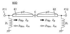
- FIGS. 1 and 2 show the case where unit cells 60A and 60B have an asymmetric T-shaped structure and an asymmetric ⁇ -shaped structure, respectively.
- 3 and 4 show, as simpler cases, the case where the unit cells 60C and 60D respectively have a symmetrical T-shaped structure and a symmetrical ⁇ -shaped structure.
- L-shaped structures are included in the case of FIG. 1 or FIG. 2 by parameter manipulation. It should be emphasized that the line lengths of the unit cells 60A to 60D with respect to the wavelength do not restrict the basic operation described here.
- the line structure shown in FIGS. 1 to 4 is simple and has predetermined line lengths (line lengths p1 and p2 in FIGS. 1 and 2 and line length p / 2 in FIGS. 3 and 4).
- a capacitive element or a capacitive network is inserted in a circuit of serial branches of a transmission line including two transmission line portions 61 and 62, and an inductive element or inductive network is inserted in a circuit of parallel branches. ing.
- capacitors C1 and C2 and an inductor L are illustrated as being inserted.
- the capacitor C and the inductors L1 and L2 are illustrated as being inserted.
- Each of the transmission line portions 61 and 62 is configured to have nonreciprocal phase shift characteristics in which the propagation constants in the forward and reverse directions are different.
- the phase constant and characteristic impedance in the forward direction meaning from the port P11 to the port P12
- ⁇ Np1 and Z p1 respectively
- the reverse direction from the port P12
- the transmission lines of FIGS. 1 and 2 have two transmission line portions 61 and 62 asymmetrical
- Equation (1) represents the relationship between the operating angular frequency ⁇ and the phase constant ⁇ , and hence becomes the dispersion relationship ( ⁇ - ⁇ diagram).
- FIG. 5 is a graph showing the dispersion curve in the non-equilibrium state in the reciprocal transmission line device according to the prior art
- FIG. 6 is a graph showing the dispersion curve in the equilibrium state in the reciprocal transmission line device according to the prior art It is.
- the graphs of FIGS. 5 and 6 show the characteristics of the angular frequency ⁇ with respect to the normalized phase constant ⁇ ⁇ p / ⁇ .
- a typical dispersion curve is represented as shown in FIG. 5, and generally right handed (RH) transmission characteristics and left handed (LH) transmission A forbidden band appears between the bands showing characteristics.
- the following two solutions are obtained as a result.
- FIG. 7 is a graph showing the dispersion curve in the non-reciprocal transmission line device according to the embodiment in the non-equilibrium state
- FIG. 8 is the dispersion curve in the non-reciprocal transmission line device according to the embodiment in the balanced state.
- the non-reciprocal transmission line device is largely different from the reciprocal transmission line device in that the axis of symmetry of the dispersion curve (indicated by an alternate long and short dash line in the figure) shifts from the ⁇ axis to the right or left.
- the nonreciprocal phase shift amount ⁇ NR is replaced with the equation (6) using forward and reverse phase constants ⁇ p and ⁇ m. It can also be expressed as As a result, it can be classified into the following five transmission bands (A) to (E).
- equation (1) becomes a quadratic equation for the angular frequency omega 2, in order not to cause the bandgap Imposing the condition of, we get
- ⁇ p and ⁇ p represent the effective effective permittivity and permeability in the forward direction in the nonreciprocal transmission line portions 61 and 62 of the unit cells 60A to 60D
- ⁇ m and ⁇ m represent those in the reverse direction.
- the condition for not causing a gap near the intersection of two modes is an impedance matching condition, similar to the case of equation (5) of the reciprocal transmission line device.
- FIG. 9 is a block diagram showing the configuration of a non-reciprocal transmission line device 70A configured by cascade-connecting the unit cells 60A of FIG.
- a plurality of unit cells 60A are cascade-connected between the port P1 and the port P2 to configure a non-reciprocal transmission line device 70A.
- FIG. 10 is a block diagram showing a configuration of a non-reciprocal transmission line device 70B configured by connecting unit cells 60B of FIG. 2 in cascade connection.
- FIG. 10 is a block diagram showing the configuration of a non-reciprocal transmission line device 70C configured by connecting unit cells 60C of FIG. 3 in cascade connection.
- FIG. 11 a plurality of unit cells 60C are connected in cascade between the port P1 and the port P2 to configure a non-reciprocal transmission line device 70C.
- FIG. 12 is a block diagram showing the configuration of a non-reciprocal transmission line device 70D configured by connecting unit cells 60D of FIG. 4 in cascade connection.
- FIG. 11 is a block diagram showing the configuration of a non-reciprocal transmission line device 70C configured by connecting unit cells 60C of FIG. 3 in cascade connection.
- FIG. 12 is a block diagram showing the configuration of a non-reciprocal transmission line device 70D configured by connecting unit cells 60D of FIG. 4 in cascade connection.
- a plurality of unit cells 60D are connected in cascade between the port P1 and the port P2 to configure a non-reciprocal transmission line device 70D. Even when a plurality of unit cells 60A to 60D are cascade-connected, it is not necessary to be necessarily configured using a single type of unit cells 60A to 60D, and unit cells of different types may be combined. It may be connected in cascade.
- the dispersion curves of the non-reciprocal transmission line devices 70A to 70E according to the present embodiment and each of the following embodiments are dispersion curves in an equilibrium state as shown in FIG. Further, in the dispersion curve of FIG. 8, the operating angular frequency ⁇ at the intersection of two modes is defined as the central angular frequency ⁇ C, and the nonreciprocal phase shift amount ⁇ NR at the intersection is defined as the nonreciprocal phase shift amount ⁇ NRC Do.
- the angular frequency corresponding to the central operating angular frequency ⁇ C in FIG. 7 also depends on the termination conditions on both sides of the transmission line, but two angular frequencies ⁇ cU corresponding to the band gap end of the dispersion curve in FIG. , ⁇ cL or the angular frequency within the band gap between them.
- FIG. 13A is a plan view showing the configuration of a circularly polarized antenna device using a non-reciprocal transmission line device 70E according to an embodiment of the present invention
- FIG. It is a perspective view which shows the structure of a part of antenna apparatus.
- the circularly polarized antenna apparatus according to the present embodiment is configured to include a non-reciprocal transmission line apparatus 70E, reflectors R1 and R2 at both ends, and a feeder F.
- Non-reciprocal transmission line device 70E arranges a microstrip line having strip conductor 12 formed on ferrite plate 15 along the circumference of disk type vertically magnetized ferrite plate 15, and includes the microstrip line
- the non-reciprocal transmission line device 70F is formed on the dielectric substrate 10 having the capacitor Cse in the series branch and the inductive short circuit stub conductor 13 in the parallel branch (the stub conductor 13 is on the back surface with the ground conductor 11) Short-circuited to the ground conductor 11) via each of The edge guide mode propagating along the microstrip line having the perpendicular magnetization ferrite plate 15 exhibits nonreciprocity in the propagation direction due to the asymmetry of the structure.
- non-reciprocal transmission line device 70F At both ends of the non-reciprocal transmission line device 70F, substantial short circuit conditions are imposed as boundary conditions. Furthermore, one end of the non-reciprocal transmission line device 70E becomes a port P1 via the capacitor 2Cse, and the feed line F is directly inserted and connected to the port P1 via the reflector R1 at a position where impedance matching can be obtained. Furthermore, the other end of the non-reciprocal transmission line device 70E is a port P2 via a capacitor 2Cse, and a reflector R2 is connected to the port P2.
- the proposed circularly polarized antenna device having the function of switching polarization rotation constitutes a circulating wave beam antenna device in a pseudo manner, and the antenna device utilizes pseudo traveling wave resonance in a nonreciprocal metamaterial structure.
- the difference from the linear non-reciprocal transmission line device according to the prior art is that the microstrip line of the circularly polarized antenna device according to the present embodiment is bent in a ring shape as illustrated in FIG. 13A. is there.
- the microstrip line is formed at the peripheral edge of the ferrite plate 15.
- Such a structure is selected for the following two reasons. Firstly, it is mentioned that the structure of the ferrite plate 15 formed of a ferrite core is simple and purely practical. The other is that by slightly increasing the magnitude of nonreciprocity, there is a possibility that phase shift can be realized by including a fringe electric field in irreversible propagation.
- the ferrite plate 15 is circular and covered with a shielding metal plate (not shown) for shielding. Here, it is not necessary to ground the shielding metal plate. The reason is that, since the electromagnetic field distribution in the ferrite plate has a symmetrical structure, the average potential on the surface of the shielding metal plate is almost zero.
- a load consisting of stub conductors 13 of parallel branches is periodically inserted in the microstrip line, and a plurality of series capacitors Cse of lumped constant are inserted in a gap along the microstrip line of the non-reciprocal transmission line device 70E.
- power is fed to the non-reciprocal transmission line device 70E from the feed line F via the reflector R1 made of a 3 ⁇ / 4 reflector and the port P1.
- the load impedance at the connection portion between the reflector R1 and the input terminal of the non-reciprocal transmission line device 70E becomes substantially zero impedance at the operating frequency.
- the reflector R1 is covered with a shielding metal plate (not shown).
- the load impedance of the reflector R2 of the other ⁇ / 4 resonator is 0 at the attachment portion of the opposite end port P2 of the non-reciprocal transmission line device 70E, and the termination short circuit condition is satisfied.
- the internal magnetization of the ferrite plate 15 is in the vertical direction from the lower surface to the upper surface, but instead of the internal magnetization of the ferrite plate 15, an external variable magnetic field is applied in the vertical direction using the external magnetic field generator 80. It is also good.
- the non-reciprocal transmission line device 70E Since the non-reciprocal transmission line device 70E is short-circuited at both ends, series resonance of the series branch is dominant during pseudo traveling wave resonance. As a result, the electric field component Ez distributed along the non-reciprocal transmission line device 70E is minimized in the area of each strip conductor 12 so that the magnitude is substantially zero.
- the magnitude of the magnetic field component Hr in the lateral direction is maximized in the same manner as the magnetic field H in the pseudo traveling wave resonator.
- the pseudo traveling wave resonator when the bias magnetic field is not applied to the ferrite plate 15, the pseudo traveling wave resonator operates as a zero-order resonator, so the magnetic field component Hr in the lateral direction has central symmetry and the magnetic field vector points in the radial direction It will be. As a result, the radiation waves from the resonator interfere and weaken, and the radiation is canceled.
- FIGS. 13A and 13B show simulation results of the non-reciprocal transmission line device 70E used in the circularly polarized antenna device of FIGS. 13A and 13B, wherein FIG. 14A is a graph showing frequency characteristics of S parameters, and FIG. It is a graph which shows a characteristic.
- the bias magnetic field Ho it is necessary for the bias magnetic field Ho to apply the ferrite plate 15 in parallel to the z axis.
- a phase shift of ⁇ 2 ⁇ radians can be achieved for the electrical length of one rotation of the split ring constituting the resonator. Due to the equal phase conditions at the two ends of the resonator, this has the interesting effect that a quasi-circulating wave is generated in the circular structure. However, in reality, it must be taken into consideration that there are gaps that divide the ring.
- Rotation of the in-plane magnetic field provides circular polarization characteristics to the beam formed in the broadside direction.
- the direction of rotation of the polarization depends on the sign of the phase shift in the resonator and can be just reversed by applying the opposite bias field Ho.
- Such a property is a new function that this kind of metamaterial antenna brings.
- the circularly polarized antenna device according to the present embodiment is connected to both ends of a nonreciprocal transmission line device 70E which is a finite length nonreciprocal phase shift right / left handed composite line and its both ends It is characterized in that the reflectors R1 and R2 and the feed line F are provided.
- the non-reciprocal transmission line device 70E constituting the quasi-traveling wave resonator is constituted of components called single or plural unit cells, is characterized by its dispersion relation, and the transmission power directions are opposite to each other.
- the dispersion curves of the right-handed mode and the left-handed mode which are related to each other, cross each other and operate in the frequency band in the band gap resulting from coupling or near the frequency where the band gap does not appear and the two dispersion curves intersect Use as a frequency.
- the operating frequency is substantially constant around the intersection frequency determined by the dispersion curve regardless of the line length constituting the resonator.
- the two reflectors R1 and R2 connected to both ends of the non-reciprocal transmission line device 70E reflect input signals respectively, and preferably are not independent of each other, (1)
- the impedance of each of the reflectors R1 and R2 is substantially zero, and specifically, a predetermined low impedance value near zero ([ ⁇ ], ohm) (0 or substantially 0).
- the low impedance value changes depending on other parameters, but is a value less than a predetermined value such as 0.1, 0.01, 0.001, etc.
- the first setting condition, (2) The admittance of each of the reflectors R1 and R2 is substantially zero, and specifically, a predetermined low admittance value in the vicinity of zero which is zero or substantially zero ([S], Siemens) (
- the low impedance value changes depending on other parameters, but is a value below a predetermined value such as 0.1, 0.01, 0.001, etc.
- the second setting condition, (3) It is set to satisfy one setting condition of the third setting condition consisting of two reactance elements which are substantially in a complex conjugate relationship with each other.
- These setting conditions are, for example, at a predetermined operating frequency or zero-order resonant frequency (1) to obtain maximum gain, (2) obtaining an axial ratio of 1 or a minimum value close to 1; (3) It is set to obtain at least one of obtaining the maximum radiation efficiency, which will be described in detail later.
- the feed line F is directly connected to a part or a plurality of locations of the resonator of the nonreciprocal transmission line device 70E, or in a state where impedance matching can be achieved through non-contact capacitive coupling or inductive coupling. Feed line for performing signal input to the
- the feed line F is directly connected to the one of the reflectors R1 at such a position that the 50 ohm transmission line can be matched.
- the central strip conductor 12 related to the serial branch and the line of the inductive stub conductor 13 constituting the parallel branch are in an orthogonal arrangement relationship with each other
- the resonant circuits of the respective branches resonate, currents flow orthogonally to each other.
- the main polarization direction in the parallel resonance of the parallel branches is orthogonal to the main polarization direction of the radiation wave in the serial resonance of the serial branches. Also, it is known that the currents flowing through these two resonant circuits are in phase, so if the resonator consists of a straight line, the radiation wave will form a linearly polarized wave even if it is superimposed, The weighting of the two orthogonal currents results in rotation of the main polarization direction.
- the nonreciprocal transmission line device 70E operating as a resonator can have a shape that is not limited to a circular shape, and each shape of a square, a rectangle, an oval, a split ring It may be a non-linear shape such as a spiral. That is, for example, the unit cells may be arranged in a one-turn ring shape having a circular shape, an elliptical shape, a square shape, or a rectangular shape, a spiral shape of a plurality of turns, or an L shape.
- the nonreciprocal transmission line device 70E constitutes a pseudo traveling wave resonator
- the measurement method of the nonreciprocal transmission line device 70E constitutes a pseudo traveling wave resonator
- the pseudo traveling wave resonator is a first traveling wave resonator.
- a current flows in a direction and a line portion A that radiates an electromagnetic wave polarized in the same direction
- a current flows in a direction (second direction) perpendicular to the current flowing in the line portion A, and is polarized in the same direction
- a line portion B that emits an electromagnetic wave that leads (or lags) the phase by 90 degrees relative to the line portion A.
- a pair of resonators whose shape is circular, square, or a split ring, spiral, etc., such that the direction of transmission power is antiparallel to the propagation of electromagnetic waves along the line in one direction (eg, forward direction).
- the phase difference between the line portions at mutually opposing positions across the substantially central portion of the nonreciprocal transmission line device 70E is approximately 180 degrees. It is necessary to adjust the phase gradient of the resonator by changing the electrical length of the series branch circuit. As a result, since the directions of power are opposite to each other and the phase relationship is opposite between the pair of line portions, the electromagnetic waves radiated from the two lines have the same polarization direction and are in the same phase.
- the fitting reinforces and forms a radiation beam.
- the resonator shape is a shape such as a spiral, and a pair or a plurality of line portions are in the same resonator such that the direction of transmission power is parallel to one-way (for example, forward) propagation of electromagnetic waves along the line. If it is present, it is necessary to adjust the phase gradient of the resonator so that the phase difference between the line portions adjacent to each other in a spiral shape is approximately 0 degrees. As a result, since the directions of power are the same and the phase relationship is in phase between the line portions, the electromagnetic waves radiated from the two lines have the same polarization direction and the same phase, and therefore, they are reinforced by superposition.
- the radiation beam is formed.
- At least one of the number of unit cells, the magnitude of the magnetization M, and the electrical length of the stub conductor 13 of the parallel branch can be changed.
- the operating point of the nonreciprocal transmission line device 70E used for the circularly polarized antenna device is not limited to the fast wave region, i.e., the leaked wave radiation region, but also the non-radiative region.
- the nonreciprocity of the nonreciprocal transmission line device 70E is relatively small and the operating point of the line is in the radiation region, leaked wave radiation from the nonreciprocal transmission line device 70E forms a radiation beam. At this time, it operates as a highly efficient leaky wave antenna using multiple reflections at both ends of the resonator. In this case, the directivity and radiation gain of the beam formed in the broadside direction can be increased as the antenna size increases.
- the nonreciprocity of the nonreciprocal transmission line device 70E when the nonreciprocity of the nonreciprocal transmission line device 70E is large and the operating point is in the non-radiative region, the leaked wave radiation from the nonreciprocal transmission line device 70E does not occur, so the propagation loss is greatly reduced. As a result, the Q value of the quasi-traveling wave resonator is increased, and the operating bandwidth is reduced. In this case, since the phase constant of the line is increased, the antenna can be made more compact than the case of the leaky wave. On the other hand, the directivity is reduced.
- the direction of rotation of the polarization (right-handed circular polarization or left-handed circular polarization) is determined by the direction of the phase gradient due to the nonreciprocity of the non-reciprocal transmission line device 70E. Furthermore, as a method of polarization rotation direction switching, the direction of the externally applied magnetic field applied to the ferrite plate 15 included in the line may be reverse in approximately the same magnitude.
- FIGS. 14A and 14B show simulation results of the non-reciprocal transmission line device 70E used in the circularly polarized antenna device of FIGS. 13A and 13B, and FIG. 14A is a graph showing frequency characteristics of S parameters. Is a graph showing dispersion characteristics.
- the present inventors examined the circularly polarized antenna device having the nonreciprocal circular structure of FIGS. 13A and 13B using numerical FEM simulation in Ansoft HFSS (registered trademark) software.
- the device was modeled using a 54 mm diameter, 0.8 mm thick YIG ferrite plate 15.
- a microstrip line having a strip conductor 12 with a width of 1 mm is formed at the circumferential edge of the ferrite plate 15 with a period of 4 mm.
- a 0.2 pF capacitor Cse is inserted between each unit cell to provide negative permeability ⁇ characteristics in the device.
- a parallel branch stub conductor 13 having a length of 1 mm and a width of 1 mm is asymmetrically loaded on each unit cell, and a strip conductor 12 which is a transmission line portion of each unit cell is formed on a ferrite plate 15.
- a circular shielding metal plate having a diameter of 41 mm is attached to the upper surface of the ferrite plate 15, where a 4 mm gap is formed between the shielding metal plate and the nonreciprocal transmission line device 70E.
- Two reflectors R1 and R2 having a line width of 0.8 mm are connected to ports P1 and P2 at each end of the nonreciprocal transmission line device 70E constituting the metamaterial resonator, and one reflector R2 is 1.2.
- the other reflector R1 has a length of 2 mm and a length of 22 mm. Power is supplied to the non-reciprocal transmission line device 70E through the reflector R1 using a feed line F having a 50 ⁇ microstrip line.
- FIG. 14A shows a relatively low insertion loss of 0.1 dB per unit cell. Most of the insertion loss contributes to the radiation.
- FIG. 15A, 15B and 15C show simulation results of the circularly polarized antenna apparatus of FIGS. 13A and 13B
- FIG. 15A is a graph showing reflection characteristics
- FIG. 15B is a graph showing normalized magnetic field distribution and electric field distribution along the longitudinal direction of the nonreciprocal transmission line device 70E including the two reflectors R1 and R2 at a frequency of 6.85 GHz
- FIG. 15C is a graph showing the phase distribution of the magnetic field Hx along the longitudinal direction of the non-reciprocal transmission line device 70E including the two reflectors R1 and R2 at a frequency of 6.85 GHz.
- FIG. 15A it shows the frequency characteristics of S 11 indicating the zero-order resonance and the first resonance.
- the input return loss (loss) in FIG. 15A has a minimum value of the zero-order resonance at 6.85 GHz, and in the upper and lower bands thereof, the minimum values due to two half-wave resonances are observed.
- the order of the resonance was confirmed from the fact that the amplitude distribution of the magnetic field H along the non-reciprocal transmission line device 70E of FIG. 15B is uniform at 6.85 GHz.
- the constant slope found in the phase distribution diagram of FIG. 15C indicates that a quasi-traveling wave resonance actually occurs at this frequency. Even in the case of a resonator using ferrite with a relatively low magnetization, it is important for practical use that a phase shift of 2 ⁇ is achieved.
- FIGS. 13A and 13B are simulation results of the circularly polarized antenna apparatus of FIGS. 13A and 13B, and FIG. 16A is a plan view showing the distribution of the magnetic field vector H on the antenna surface, and FIG. 16B is the electric field distribution on the antenna surface It is a photograph showing.
- FIG. 16D the higher the hatching density, the greater the electric field.
- FIG. 16D shows a three-dimensional radiation pattern showing a cross section in radiation pattern characteristics, and the rotation of the electric field vector E of the beam in the broadside direction is observed.
- the dark part indicates that the electric field is relatively large, while the thin part indicates that the electric field is relatively small.
- 90 is a metal shielding plate.
- the magnetic field vector H is generated by the metamaterial transmission line of the antenna and is illustrated using the vectors of FIG. 16A, where the points that are nearly uniform in one direction determine the cross polarization plane. Although it can not be determined whether the distribution of the rotating magnetic field vector H indicates the uniformity of the amplitude, the characteristic diagram of the electric field component Ez in FIG. 16B confirms the uniformity of the electric field in the circularly polarized antenna device. be able to. From the radiation pattern of FIG. 16C, narrow beam radiation with a gain of approximately 11 dBi can be identified.
- the gap between the end ports P1 and P2 of the nonreciprocal transmission line device 70E causes disturbance to the electromagnetic field distribution. According to the simulation results, electromagnetic field radiation exhibits almost perfect circular polarization characteristics. Also, depending on the applied DC magnetic field, the circularly polarized antenna device operates as a nonreciprocal left handed transmission line antenna when magnetization M is parallel to the z direction, and magnetization is parallel to the opposite direction -z When M, it operates as a nonreciprocal right-handed transmission line antenna.
- FIG. 17A is a plan view showing the configuration of a circularly polarized antenna device using a non-reciprocal transmission line device 70F according to an embodiment of the present invention.
- FIG. 17B is an enlarged perspective view showing a part of the configuration of FIG. 17A.
- a yttrium-iron-garnet (YIG) polycrystal circular ferrite plate 15 of 1.0 mm thickness and 32.0 mm diameter is placed on the center of the ground conductor 11, and further, the upper surface of the ferrite plate 15 is At the edge, a non-reciprocal transmission line device 70F, which is a right-hand / left-handed composite line consisting of a circular microstrip line, is configured.
- a 0.8 mm thick dielectric substrate 10 is placed on the outside of the ferrite plate 15 on the ground conductor 11, and is periodically inserted into the circular line so that the effective dielectric constant of the structure becomes negative.
- the shunt branch short stub conductor 13 is formed on this dielectric substrate 10.
- each stub conductor 13 is connected to the ground conductor 11 via the via conductor 13C and shorted.
- the parameters of the non-reciprocal transmission line apparatus 70F which is a prototype right-hand / left-handed composite line are as follows.
- the length and width of the stub conductor 13 are respectively 1.3 mm and 1.0 mm.
- the number of unit cells constituting the resonator is 21 cells.
- FIG. 18 is a graph showing the reflection characteristic of the circularly polarized antenna device of FIG. 17A.
- the YIG which is a soft magnetic material, can be treated as an isotropic dielectric because the effective magnetization is substantially zero when no magnetic field is applied.
- the right-hand / left-handed composite line of the nonreciprocal transmission line device 70F exhibits reciprocity, and the magnitude and the phase of the electromagnetic field distribution on the line become uniform at the time of zero-order resonance.
- the reflection characteristic of the antenna device observed at the feed line F at this time is shown in FIG. In FIG. 18, not only measurement results but also numerical calculation results of simulation are shown together for comparison. From the result of the numerical simulation of the electromagnetic field distribution, it is confirmed that the zero-order resonance characteristic is exhibited when the frequency is 5.0 GHz.
- FIG. 19 is a graph showing a first example of the dispersion characteristic of the non-reciprocal transmission line device 70E of FIG. 17A.
- FIG. 20 is a graph showing a second example of the dispersion characteristic of the non-reciprocal transmission line device 70E of FIG. 17A.
- the dispersion characteristics of the nonreciprocal right / left handed composite transmission line of the nonreciprocal transmission line device 70E designed and manufactured are shown in FIG.
- FIG. 21 is a graph showing the phase of the electromagnetic field with respect to the position in the resonator in the circularly polarized antenna device of FIG. 17A.
- the reason why the case of effective magnetization ⁇ 0 Ms 95 mT is selected as the numerical calculation result in FIG. 19 will be described with reference to FIG. 21.
- FIG. 21 shows the phase distribution of the electromagnetic field observed along the longitudinal direction of the nonreciprocal transmission line device 70F which is a ring-shaped combined right / left handed line.
- the electromagnetic wave radiated from the line exhibits circular polarization characteristics when the phase difference when the traveling wave goes around is 360 degrees. ing. From FIG.
- FIG. 22 is a graph showing a first example of reflection characteristics of the circularly polarized antenna device of FIG. 17A.
- FIG. 23 is a graph showing a second example of the reflection characteristic of the circularly polarized antenna device of FIG. 17A.
- FIG. 23 shows the reflection characteristics from the feed line when a DC magnetic field is applied in the reverse direction to that of FIG.
- FIGS. 24A, 24B, 24C, and 24D are radiation pattern diagrams showing first to fourth examples of the radiation characteristics of the circularly polarized antenna device of FIG. 17A, respectively.
- FIGS. 24A and 24C show the xz plane
- the radiation patterns in the yz plane are shown in 24B and 24D, respectively.
- FIGS. 24A and 24B when the effective magnetization is positive, a radiation beam of right circular polarization is formed in the broadside direction, and as can be seen from FIGS. 24C and 24D.
- a left circularly polarized radiation beam is formed in the side direction.
- the rotational direction of the circularly polarized wave can be switched by switching the direction of magnetization.
- FIGS. 25A, 25B, 25C and 25D are radiation pattern diagrams showing fifth to eighth examples of the radiation characteristics of the circularly polarized antenna device of FIG. 17A, respectively.
- FIGS. 25A and 25C the xz plane.
- FIGS. 25B and 25D respectively show radiation patterns in the yz plane. As can be seen from FIGS.
- FIG. 26A is a plan view showing the configuration of a circularly polarized antenna device using a non-reciprocal transmission line device 70G having an L-shaped shape according to an embodiment of the present invention.
- FIG. 26B is an enlarged perspective view showing a part of the configuration of FIG. 26A.
- a nonreciprocal transmission line device 70G which is a nonreciprocal right / left handed composite line of a finite length, is bent at 90 degrees near the center, and its both ends have a quarter wavelength Microstrip lines are connected as shorting reflectors R1 and R2. Furthermore, the feed line F is directly connected to the reflector R1 at a point where impedance matching can be made. The structural parameters used for the design are shown below.
- the width and length of the periodically inserted stub conductors 13 are 0.67 mm and 1.6 mm, respectively.
- Cse 0.6 pF as the capacitance of the chip capacitor Cse periodically inserted in the series branch.
- the thickness of the dielectric substrate 10 is 0.8 mm.
- the number of unit cells in forming the L-type resonator is ten.
- FIG. 27 is a graph showing the propagation characteristics of the non-reciprocal transmission line device 70G of FIG. 26A.
- the operating frequency of the antenna is around 6.7 GHz.
- FIG. 28 is a graph showing the reflection characteristic of the circularly polarized antenna device of FIG. 26A.
- FIG. 28 shows the reflection characteristics of the circularly polarized antenna device as viewed from the feed line F when the number of unit cells is 10.
- the phase difference between the middle point of the line portion parallel to the y axis and the middle point of the line portion parallel to the z axis is 90 degrees.
- the radiation wave from the resonator is circularly polarized when the phase difference between the two ends of the L-shaped line is 180 degrees.
- a plurality of notches correspond to resonance states, and in particular, it is confirmed from numerical calculation results of electromagnetic field distribution that resonance at a frequency of 6.7 GHz corresponds to pseudo traveling wave resonance.
- 29A and 29B are radiation pattern diagrams showing first and second examples of radiation characteristics of the circularly polarized antenna apparatus of FIG. 26A, respectively.
- 29A and 29B show radiation patterns from the circularly polarized antenna device at a frequency of 6.7 GHz.
- FIG. 30 is a plan view showing the configuration of a circularly polarized antenna apparatus using the non-reciprocal transmission line apparatus 70H according to the embodiment of the present invention.
- FIG. 30 to FIG. 36 the same components as those in the above embodiment are given the same reference numerals.
- FIG. 30 shows a quasi traveling wave resonator in the case where the non-reciprocal transmission line device 70H is formed in a semicircular shape on the circular ferrite substrate 15. If the phase difference between the two current components orthogonal to each other in the nonreciprocal transmission line device part becomes circularly polarized radiation if the phase difference becomes 90 degrees, as shown in FIG. 30, even the semicircular nonreciprocal transmission line device is circularly polarized radiation Is possible.
- FIG. 31 is a plan view showing the configuration of a circularly polarized antenna device using a non-reciprocal transmission line device 70I according to an embodiment of the present invention.
- FIG. 31 shows a circularly polarized antenna apparatus in which two transmission lines TL1 and TL2 having different propagation characteristics and lengths are connected in an L shape.
- the ratio of lengths of orthogonal transmission lines TL1 and TL2 is determined according to the difference in the radiation power from the two types of lines TL1 and TL2, and the phase difference between the middle points of the respective transmission lines TL1 and TL2 is 90 degrees
- the respective phase gradients in the transmission lines TL1 and TL2 are set so that
- FIG. 32 is a plan view showing the configuration of a circularly polarized antenna device using the non-reciprocal transmission line device 70J according to the embodiment of the present invention.
- FIG. 32 shows a configuration example of a pseudo traveling wave resonator when the non-reciprocal transmission line device 70J is configured in an elliptical shape.
- the non-reciprocal transmission line device 70J is configured to include sections S1 and S1 of a pair of straight line portions facing each other and sections S2 and S2 of a pair of curved line portions facing each other.
- the structural parameters of the unit cells constituting the nonreciprocal transmission line device 70J are not uniform along the longitudinal direction of the transmission line but become nonuniform, but the intersection points of the dispersion curves of all unit cells have almost the same frequency It is designed to be The ratio of the major and minor axes of the ellipse is determined by the difference in the radiation power from the nonuniformly distributed unit cells.
- FIG. 33 is a plan view showing the configuration of a circularly polarized antenna device using the non-reciprocal transmission line device 70K according to the embodiment of the present invention.
- a circle is formed of a rectangular pseudo traveling wave resonator, having a structure in which two sets of L-type nonreciprocal transmission line devices 70I consisting of two types of transmission lines TL1 and TL2 shown in FIG. 31 are connected in series.
- a polarization antenna device is configured.
- FIG. 34 is a plan view showing the configuration of a circularly polarized antenna device using the non-reciprocal transmission line device 70L according to the embodiment of the present invention.
- FIG. 34 shows a circularly polarized antenna device when the non-reciprocal transmission line device 70L is formed in a spiral shape on the circular ferrite substrate 15.
- FIG. 35 is a plan view showing the configuration of a circularly polarized antenna device using a non-reciprocal transmission line device 70M according to an embodiment of the present invention.
- FIG. 35 shows a circularly polarized antenna device in a case where a pseudo traveling wave resonator is formed of two types of circular nonreciprocal transmission line devices 70M1 and 70M2 having different propagation characteristics in a concentric manner.
- both the non-reciprocal transmission line device 70M1 having a small radius of curvature and the non-reciprocal transmission line device 70M2 having a large radius of curvature have a phase difference of 360 degrees with respect to wave propagation for one turn. It is necessary to have a phase gradient. Therefore, it is necessary to set the inner non-reciprocal transmission line device 70M1 so that the phase constant is larger than that of the outer non-reciprocal transmission line device 70M2.
- FIG. 36 is a plan view showing the configuration of a circularly polarized antenna device using the non-reciprocal transmission line device 70N according to the embodiment of the present invention.
- a shunt branch is induced outside the circular line as in the prior art.
- the stub conductor 13 is periodically inserted, whereas in the other non-reciprocal transmission line device 70N1 installed inside, the shunt branch induction stub conductor 13 is inserted inside the circular line.
- a metal loop for an external DC applied magnetic field is inserted between the two circular nonreciprocal transmission line devices 70N1 and 70N2.
- a current I is applied to the metal loop, a magnetic field is generated in the direction of the right-handed screw, so that the magnetic field component perpendicular to the ferrite substrate 15 reverses in direction inside and outside the metal loop. .
- Non-reciprocity results in the same direction.
- the radiation from the two circular nonreciprocal transmission line devices 70N1 and 70N2 is polarized and rotated in the same direction.
- the case where the stub conductor 13 is inserted is the case of the inner circular line and the outer circular line
- the insertion side may be the opposite combination. That is, the stub conductor 13 is inserted outside the circular line in the inner circular nonreciprocal transmission line device 70N1, and the stub conductor 13 is inserted inside the circular line in the outer circular nonreciprocal transmission line device 70N2. It may be a structure.
- FIG. 37 is a table showing simulation results when the reflector length L_Refl is changed in the ring type circularly polarized antenna device using the non-reciprocal transmission line device 70F of FIG. 17A. . That is, FIG. 37 shows the case where the characteristics of the reflector R2 on the side to which the feed line F is not inserted is changed among the two reflectors R1 and R2 inserted on both sides of the pseudo traveling wave resonator. It shows the center frequency of the traveling wave resonance, the antenna radiation gain, the axial ratio and the radiation efficiency.
- Each of the reflectors R1 and R2 is composed of a finite-length open-ended microstrip line, and operates as a variable reactive element by changing the line length.
- the impedance is infinite (admittance is 0)
- the line length is sufficiently short compared to the wavelength, a capacitive element
- the impedance is It operates as a near zero short circuit element, an inductive element if it is longer than a quarter wavelength but shorter than a half wavelength.
- the operating frequency is 4.95 GHz from the dispersion relation of the non-reciprocal transmission line device 70F, but at this time, the length of 1 ⁇ 4 (inside the line) wavelength ⁇ g is 4.5 mm.
- the operating frequency of the circularly polarized antenna device is 5.14 GHz as can be seen from the table of FIG. From FIG. 37, it can be read that the operating frequency tends to be higher as the length of the microstrip line constituting the reflector R2 is shorter. That is, as the reactance of one of the reflectors R2 is a negative value and the absolute value becomes larger, the resonance frequency is shifted to the higher frequency side.
- the cause of this may be the problem of the manufacturing accuracy of the non-reciprocal transmission line device 70F.
- the dispersion curve of the nonreciprocal transmission line device 70F in the prototype resonator although an attempt is made to design so that there is no band gap, there is actually a band gap, and the operation is performed due to changes in reflection conditions at both ends of the resonator. It is considered that the point is moving in the band gap.
- the band width of the band gap is the frequency domain sandwiched by two resonance frequencies: series resonance of series branch in the case of short circuit at both ends and shunt branch parallel resonance in the case of open both ends;
- series resonance of series branch in the case of short circuit at both ends
- shunt branch parallel resonance in the case of open both ends
- the parallel resonance frequency of the shunt branch is higher than the series branch series resonance frequency due to the short circuit at both ends, it is considered that the operating frequency increases as the reactance of the reflective element increases.
- Another factor that causes the resonance frequency to shift to the higher frequency side is considered to be that it deviates largely from the zero-order resonance condition because only the structural parameter of one of the reflectors is changed.
- the operating frequency of the resonator fluctuates with the fluctuation of the characteristics of the reflector R2 in this way, the way of the fluctuation is also large due to the manufacturing accuracy of the right-hand / left-handed composite line constituting the resonator. It will be different.
- the axial ratio is the lowest and the radiation efficiency is the highest when the reflector length is 4.5 mm, that is, it is closest to the short circuit at both ends.
- FIG. 38 is a table showing simulation results when the reflector length L_Refl is changed in the circularly polarized antenna device using the L-type non-reciprocal transmission line device 70I of FIG. That is, FIG. 38 shows the case where the characteristics of the reflector R2 on the side where the feed line F is not inserted is changed among the two reflectors R1 and R2 inserted on both sides of the pseudo traveling wave resonator. It shows the center frequency of the traveling wave resonance, the antenna radiation gain, the axial ratio and the radiation efficiency.
- Each of the reflectors R1 and R2 is composed of a finite-length open-ended microstrip line, and operates as a variable reactive element by changing the line length.
- the impedance When the line length is 0, the impedance is infinite (admittance is 0), when the line length is sufficiently short compared to the wavelength, a capacitive element, and when the length is a quarter wavelength (in the line), the impedance is It operates as a near zero short circuit element, an inductive element if it is longer than a quarter wavelength but shorter than a half wavelength.
- the operating frequency is 5.8 GHz, but at this time, the length of the 1/4 (in-line) wavelength ⁇ g is 8.5 mm.
- the operating frequency of the circularly polarized antenna device became 6.02 GHz, as can be seen from the table of FIG. It can be seen from FIG. 38 that the operating frequency tends to be higher as the length of the microstrip line constituting the reflector R2 is shorter. That is, as the reactance of one of the reflectors R2 is a negative value and the absolute value becomes larger, the resonance frequency is shifted to the higher frequency side.
- the cause of this may be the problem of the manufacturing accuracy of the non-reciprocal transmission line device 70F.
- the dispersion curve of the nonreciprocal transmission line device 70F in the prototype resonator although an attempt is made to design so that there is no band gap, there is actually a band gap, and the operation is performed due to changes in reflection conditions at both ends of the resonator. It is considered that the point is moving in the band gap.
- the band width of the band gap is the frequency domain sandwiched by two resonance frequencies: series resonance of series branch in the case of short circuit at both ends and shunt branch parallel resonance in the case of open both ends;
- series resonance of series branch in the case of short circuit at both ends
- shunt branch parallel resonance in the case of open both ends
- the parallel resonance frequency of the shunt branch is higher than the series branch series resonance frequency due to the short circuit at both ends, it is considered that the operating frequency increases with the increase in the reactance of the reflective element.
- Another factor that causes the resonance frequency to shift to the higher frequency side is considered to be that the structure parameter of one of the resonators is changed, and therefore it deviates largely from the zero-order resonance condition.
- the manner of the fluctuation depends on the manufacturing accuracy of the right-hand / left-handed composite line constituting the resonator. Will also differ greatly.
- the radiation efficiency is the highest when the reflector length is 8.5 mm, that is, closest to the short circuit at both ends, but the gain is the highest near that. Is the case where the reflector length is 7.5 mm, and the axial ratio becomes the lowest when the reflector tension is 9.5 mm.
- the operating frequency of the quasi-traveling wave resonator configured by the nonreciprocal transmission line devices 70E to 70N is the nonreciprocal transmission line device 70E that configures the resonator. It can be estimated from the dispersion characteristic of 70N. Therefore, the resonance characteristics of the designed structure were examined centering on this estimated frequency. As a result, a resonant state showing a desired electromagnetic field distribution was obtained near the estimated frequency. The distribution of magnetic field vectors obtained by numerical calculation at that time is shown in FIG. 16A. It was confirmed that the radiation from the non-reciprocal transmission line devices 70E to 70N exhibited circular polarization characteristics as a result of reinforcing in one direction without canceling each other.
- the circularly polarized antenna apparatus of the quasi-circulating wave according to the present embodiment can be formed as a compact and lightweight antenna apparatus, so that the application area of the circularly polarized antenna can be greatly expanded, and the polarization can be switched dynamically.
- the rotation is not constrained in a predetermined direction.
- the antenna device concept can be used for mobile applications with rapidly changing environmental conditions that provide high reliability of the communication link. The same can be used to switch between LHCP and RHCP beams on demand and facilitate detection of objects with small radar cross sections, objects with anomalous electromagnetic surface coatings, or complex environments There is also a possible radar application available.
- a non-reciprocal transmission line device for a circularly polarized antenna device capable of radiating circularly polarized electromagnetic waves, and a compact and lightweight circularly polarized antenna device as compared with the prior art. be able to.
Landscapes
- Engineering & Computer Science (AREA)
- Computer Networks & Wireless Communication (AREA)
- Signal Processing (AREA)
- Power Engineering (AREA)
- Variable-Direction Aerials And Aerial Arrays (AREA)
- Waveguide Aerials (AREA)
- Waveguides (AREA)
Abstract
Description
上記各単位セルは非線形形状で配置され、
上記各単位セルは、上記マイクロ波の伝搬方向に対して異なる方向に磁化されてジャイロ異方性(ジャイロトロピック異方性ともいい、磁化によりマイクロ波の伝搬定数が伝搬方向により異なった影響を受ける性質をいう)を有するように自発磁化を有するか又は外部磁界により磁化される伝送線路部分を有し、
上記非相反伝送線路装置は、上記マイクロ波が、上記非相反伝送線路装置に沿って伝送される伝送電力の方向が互いに逆方向の関係にある右手系モードと左手系モードの分散曲線が互いに交差し、結合の結果生じるバンドギャップ内の周波数帯域、もしくはバンドギャップが現れず2本の分散曲線の交点となる周波数付近を動作周波数として利用して伝搬するように構成され、
上記非相反伝送線路装置は、上記非相反伝送線路装置の両端のそれぞれに接続され、入力される信号を反射する第1及び第2の反射器を備えたことを特徴とする。
上記擬似進行波共振器は、所定の第1の方向に電流を流し、上記第1の方向に偏波した電磁波を放射する第1の線路部分と、上記第1の線路部分に流れる電流に対して実質的に直交する垂直方向である第2の方向に電流を流し、上記第2の方向に偏波していて、しかも、上記第1の線路部分よりも位相が90度進み、もしくは遅れる電磁波を放射する第2の線路部分を含むことを特徴とする。
上記非相反伝送線路装置と、
上記第1の反射器に接続された給電線とを備えた円偏波アンテナ装置であって、
上記非相反伝送線路装置の非可逆性に起因する位相勾配の方向に依存して、右旋円偏波又は左旋円偏波の電磁波を放射することを特徴とする。
(1)インピーダンスが0、もしくは所定値以下の値を有するインピーダンスである第1の設定条件と、
(2)アドミタンスが0、もしくは所定値以下の値を有するアドミタンスである第2の設定条件と、
(3)互いに複素共役の関係を有するリアクタンス素子を有する第3の設定条件と
のうちの1つの設定条件を満たすように構成されたことを特徴とする。
直線偏波のアンテナは通常、比較的シンプルなデザインと優れたアンテナ利得を提供する。偏波面の選択は、無線チャネルの簡単な分離のために使用することができる。しかし、直線偏波は、地形又は強い電波干渉上の高密度な障害物と無線局を対向させたときには、偏波面が変化したり、電波が減衰すること等により受信感度が低下するという弱点になる。例えば、直線偏波チャネルはマルチパス干渉から保護されず、また特定の方向で直線格子形状の電波障害物を電波が通過する場合にも、容易に抑圧されてしまう。直線偏波のビームはまた、人工塗料、コーティングなど、近代的な建築材料においては一般的な異方性及び半導体特性を有する傾斜面に出会うとき、しばしば、人工環境において変化する。直線偏波から偏波面の楕円化及び回転の変化は、通信チャネル又はレーダー応答に悪影響を与えることもありうる。
まず始めに、本実施形態に係る円偏波アンテナ装置で用いる非相反伝送線路装置(非可逆伝送線路装置ともいう。)の基本構成及び動作原理について、図1~図12を参照して説明する。なお、本明細書中で用いた数式については、各式の後に示した丸括弧でくくられた番号を参照する。


(B)順方向が左手系伝送、逆方向は伝搬定数がゼロで管内波長が無限大となる。
(C)順方向が左手系伝送、逆方向が右手系伝送(RH/LH)。
(D)順方向が右手系伝送、逆方向は伝搬定数がゼロで管内波長が無限大となる。
(E)順方向及び逆方向伝搬共に右手系伝送(RH/RH)。但し、伝搬定数の大きさは互いに異なる。


図13Aは本発明の実施形態に係る非相反伝送線路装置70Eを用いた円偏波アンテナ装置の構成を示す平面図であり、図13Bは図13Aの円偏波アンテナ装置の一部分の構成を示す斜視図である。本実施形態に係る円偏波アンテナ装置は、非相反伝送線路装置70Eと、両端の反射器R1,R2と、給電線Fとを備えて構成される。非相反伝送線路装置70Eは、円板型の垂直磁化フェライト板15の円周に沿って、フェライト板15上に形成されたストリップ導体12を有するマイクロストリップ線路を配置し、当該マイクロストリップ線路を含む非相反伝送線路装置70Fは直列枝にキャパシタCseを、並列枝に誘導性短絡スタブ導体13(スタブ導体13は、裏面に接地導体11を有する誘電体基板10上に形成され、先端はビア導体13Cを介して接地導体11に短絡される)を、それぞれ周期的に挿入した構造を有する。垂直磁化フェライト板15を有するマイクロストリップ線路に沿って伝搬するエッジガイドモードは、構造の非対称性により伝搬方向により非相反性を示す。非相反伝送線路装置70Fの両端には、境界条件として実質的な短絡条件が課されている。さらに、非相反伝送線路装置70Eの一端はキャパシタ2Cseを介してポートP1となり、当該ポートP1には反射器R1を介して給電線Fがインピーダンス整合の取れる位置に直接挿入接続されている。また、さらに、非相反伝送線路装置70Eの他端はキャパシタ2Cseを介してポートP2となり、当該ポートP2には反射器R2が接続されている。
本実施形態に係る円偏波アンテナ装置は、有限長の非相反移相右手/左手系複合線路である非相反伝送線路装置70Eとその両端に接続された反射器R1,R2、さらに給電線Fを備えることを特徴とする。擬似進行波共振器を構成する非相反伝送線路装置70Eは、単一もしくは複数の単位セルと呼ばれる構成要素から構成されており、その分散関係に特徴を有し、伝送電力の方向が互いに逆方向の関係にある右手系モードと左手系モードの分散曲線が互いに交差し、結合の結果生じるバンドギャップ内の周波数帯域、もしくはバンドギャップが現れず2本の分散曲線の交点となる周波数付近を、動作周波数として利用する。動作周波数は、共振器を構成する線路長によらず、分散曲線によって決まる交点周波数付近でほぼ一定となる。
(1)各反射器R1,R2のインピーダンスが実質的に0であって、具体的には、0、もしくは実質的に0である0近傍の所定の低インピーダンス値([Ω]、オーム)(ここで、当該低インピーダンス値は他のパラメータにより変化するが、例えば0.1、0.01、0.001などである所定値以下の値である)である、実質的に両端短絡状態である第1の設定条件と、
(2)各反射器R1,R2のアドミタンスが実質的に0であって、具体的には、0、もしくは実質的に0である0近傍の所定の低アドミタンス値([S]、ジーメンス)(ここで、当該低インピーダンス値は他のパラメータにより変化するが、例えば0.1、0.01、0.001などである所定値以下の値である)である、実質的に両端開放状態である第2の設定条件と、
(3)互いに実質的に複素共役の関係にある2つのリアクタンス素子からなる第3の設定条件と
のうちの1つの設定条件を満たすように設定される。これら設定条件は、例えば、所定の動作周波数又は0次共振周波数において、
(1)最大利得を得ること、
(2)軸比が1又は1に近い最低値を得ること、
(3)最大放射効率を得ること
のうちの少なくとも1つを得るように設定され、これについて詳細後述される。
図14A及び図14Bは図13A及び図13Bの円偏波アンテナ装置で用いる非相反伝送線路装置70Eのシミュレーション結果であって、図14AはSパラメータの周波数特性を示すグラフであり、図14Bは分散特性を示すグラフである。
本発明者らは、円偏波アンテナ装置を試作して実験及びシミュレーションを行った。これについて以下説明する。
図26Aは本発明の実施形態に係る、L型形状を有する非相反伝送線路装置70Gを用いた円偏波アンテナ装置の構成を示す平面図である。また、図26Bは図26Aの一部の構成を示す拡大斜視図である。
図30は本発明の実施形態に係る非相反伝送線路装置70Hを用いた円偏波アンテナ装置の構成を示す平面図である。なお、図30~図36において、上述の実施形態と同様の構成要素について同一の符号を付す。図30において、円形のフェライト基板15上に半円型に非相反伝送線路装置70Hを構成した場合の擬似進行波共振器を示す。非相反伝送線路装置部分において直交する2つの電流成分の位相差が90度となれば円偏波放射となるため図30に示したように半円型の非相反伝送線路装置でも円偏波放射が可能である。
図37は図17Aの非相反伝送線路装置70Fを用いたリング型円偏波アンテナ装置において反射器長L_Reflを変化したときのシミュレーション結果を示す表である。すなわち、図37は、擬似進行波共振器の両側に挿入された2つの反射器R1,R2のうち、給電線Fの挿入されていない側の反射器R2の特性を変化させた場合の、擬似進行波共振の中心周波数、アンテナ放射利得、軸比及び放射効率を示したものである。各反射器R1,R2は、有限長一端開放マイクロストリップ線路で構成され、線路の長さを変えることにより、可変リアクティブ素子として動作する。線路長が0のときは、インピーダンスが無限大(アドミタンスが0)、線路長が波長に比べて十分短いときは容量性素子、長さが4分の1(線路内)波長のときはインピーダンスがほぼ0の短絡素子、4分の1波長よりも長いが2分の1波長よりも短い場合は誘導性素子として動作する。
以上説明したように、本実施形態によれば、非相反伝送線路装置70E~70Nにより構成される擬似進行波共振器の動作周波数は共振器を構成する非相反伝送線路装置70E~70Nの分散特性から推定できる。そこで、この推定される周波数を中心に設計構造の共振特性を調べた。その結果、推定される周波数の近傍で、所望の電磁界分布を示す共振状態が得られた。そのときに数値計算により得られた磁界ベクトルの分布を図16Aに示す。非相反伝送線路装置70E~70Nからの、放射は打ち消し合うことなく、単方向に強め合う結果、円偏波特性を示すことが確認された。
11…接地導体、
12…ストリップ導体、
13…スタブ導体、
13C…ビア導体、
15…フェライト板、
60A~60D…単位セル、
61,62…伝送線路部分、
70A~70N,70M1,70M2,70N1,70N2…非相反伝送線路装置、
80…外部磁界発生器、
C,C1,C2,C60,Cse…キャパシタ、
F…給電線、
L,L1~L6…インダクタンス、
P1,P2,P11,P12…ポート、
R1,R2…反射器、
S1~S12…セクション、
TL1,TL2…伝送線路。
Claims (9)
- マイクロ波の伝送線路部分と、容量性素子を等価的に含む直列枝の回路と、上記伝送線路部分からそれぞれ分岐して設けられかつ誘導性素子を等価的に含む並列枝の回路とを有する少なくとも1つの単位セルを、第1と第2のポートの間で縦続接続して構成され、順方向の伝搬定数と逆方向の伝搬定数とが互いに異なる非相反伝送線路装置において、
上記各単位セルは非線形形状で配置され、
上記各単位セルは、上記マイクロ波の伝搬方向に対して異なる方向に磁化されてジャイロ異方性を有するように自発磁化を有するか又は外部磁界により磁化される伝送線路部分を有し、
上記非相反伝送線路装置は、上記マイクロ波が、上記非相反伝送線路装置に沿って伝送される伝送電力の方向が互いに逆方向の関係にある右手系モードと左手系モードの分散曲線が互いに交差し、結合の結果生じるバンドギャップ内の周波数帯域、もしくはバンドギャップが現れず2本の分散曲線の交点となる周波数付近を動作周波数として利用して伝搬するように構成され、
上記非相反伝送線路装置は、上記非相反伝送線路装置の両端のそれぞれに接続され、入力される信号を反射する第1及び第2の反射器を備えたことを特徴とする非相反伝送線路装置。 - 上記非相反伝送線路装置は擬似進行波共振器を構成し、
上記擬似進行波共振器は、所定の第1の方向に電流を流し、上記第1の方向に偏波した電磁波を放射する第1の線路部分と、上記第1の線路部分に流れる電流に対して実質的に直交する垂直方向である第2の方向に電流を流し、上記第2の方向に偏波していて、しかも、上記第1の線路部分よりも位相が90度進み、もしくは遅れる電磁波を放射する第2の線路部分を含むことを特徴とする請求項1記載の非相反伝送線路装置。 - 上記各単位セルを、円形状、楕円形状、正方形状、又は長方形状を有する一巻きリング形状、複数回巻きのスパイラル形状、もしくはL型形状で配置したことを特徴とする請求項1又は2記載の非相反伝送線路装置。
- 請求項1~3のうちのいずれか1つに記載の非相反伝送線路装置と、
上記第1の反射器に接続された給電線とを備えた円偏波アンテナ装置であって、
上記非相反伝送線路装置の非可逆性に起因する位相勾配の方向に依存して、右旋円偏波又は左旋円偏波の電磁波を放射することを特徴とする円偏波アンテナ装置。 - 上記磁化の方向を互いに逆方向に切り替えることにより、右旋円偏波又は左旋円偏波の電磁波を放射することを特徴とする請求項4記載の円偏波アンテナ装置。
- 上記各単位セルによりそれぞれ形成される複数の線路部分のうち、上記非相反伝送線路装置の略中心部を挟んで互いに対向する位置にある各1対の線路部分の位相勾配を、当該各1対の線路部分間の位相差が実質的に180度となるように調整することで放射ビームを放射することを特徴とする請求項4又は5記載の円偏波アンテナ装置。
- 上記各単位セルによりそれぞれ形成される複数の線路部分のうち、上記非相反伝送線路装置の略中心部を挟んで互いに同じ側にある隣接する位置にある各1対の線路部分の位相勾配を、当該各1対の線路部分間の位相差が実質的に0度となるように調整することで放射ビームを放射することを特徴とする請求項4又は5記載の円偏波アンテナ装置。
- 上記位相勾配を、上記単位セルの数と、上記磁化の大きさと、上記並列枝の回路の電気長とのうちの少なくとも1つを変化させて調整することを特徴とする請求項6又は7記載の円偏波アンテナ装置。
- 上記第1及び第2の反射器はそれぞれ、
(1)インピーダンスが0、もしくは所定値以下の値を有するインピーダンスである第1の設定条件と、
(2)アドミタンスが0、もしくは所定値以下の値を有するアドミタンスである第2の設定条件と、
(3)互いに複素共役の関係を有するリアクタンス素子を有する第3の設定条件と
のうちの1つの設定条件を満たすように構成されたことを特徴とする請求項4~8のうちのいずれか1つに記載の円偏波アンテナ装置。
Priority Applications (2)
| Application Number | Priority Date | Filing Date | Title |
|---|---|---|---|
| US15/121,530 US10014903B2 (en) | 2014-02-27 | 2015-02-25 | Non-reciprocal transmission apparatus with different backward and forward propagation constants, provided for circularly polarized wave antenna apparatus |
| JP2016505267A JP6449237B2 (ja) | 2014-02-27 | 2015-02-25 | 非相反伝送線路装置 |
Applications Claiming Priority (2)
| Application Number | Priority Date | Filing Date | Title |
|---|---|---|---|
| JP2014-036943 | 2014-02-27 | ||
| JP2014036943 | 2014-02-27 |
Publications (1)
| Publication Number | Publication Date |
|---|---|
| WO2015129757A1 true WO2015129757A1 (ja) | 2015-09-03 |
Family
ID=54009072
Family Applications (1)
| Application Number | Title | Priority Date | Filing Date |
|---|---|---|---|
| PCT/JP2015/055434 WO2015129757A1 (ja) | 2014-02-27 | 2015-02-25 | 非相反伝送線路装置 |
Country Status (3)
| Country | Link |
|---|---|
| US (1) | US10014903B2 (ja) |
| JP (1) | JP6449237B2 (ja) |
| WO (1) | WO2015129757A1 (ja) |
Cited By (6)
| Publication number | Priority date | Publication date | Assignee | Title |
|---|---|---|---|---|
| JP2017152878A (ja) * | 2016-02-24 | 2017-08-31 | 国立大学法人京都工芸繊維大学 | アンテナ装置 |
| JP2017184111A (ja) * | 2016-03-31 | 2017-10-05 | 国立大学法人京都工芸繊維大学 | 非相反メタマテリアル伝送線路装置及びアンテナ装置 |
| WO2018180876A1 (ja) * | 2017-03-28 | 2018-10-04 | セイコーソリューションズ株式会社 | 円偏波アンテナ |
| WO2019172192A1 (ja) * | 2018-03-05 | 2019-09-12 | 国立大学法人京都工芸繊維大学 | 非相反伝送線路装置及びアンテナ装置 |
| JP2019153978A (ja) * | 2018-03-05 | 2019-09-12 | 国立大学法人京都工芸繊維大学 | 軌道角運動量モード擬似進行波共振器及び軌道角運動量アンテナ装置 |
| JP2020036096A (ja) * | 2018-08-27 | 2020-03-05 | 国立大学法人京都工芸繊維大学 | 擬似進行波共振器及びアンテナ装置 |
Families Citing this family (2)
| Publication number | Priority date | Publication date | Assignee | Title |
|---|---|---|---|---|
| WO2020144740A1 (ja) * | 2019-01-08 | 2020-07-16 | 三菱電機株式会社 | 伝送路設計支援装置、伝送路設計支援方法及びプログラム |
| CN112928420B (zh) * | 2021-03-12 | 2022-06-10 | 南通大学 | 一种金属凹嵌式太赫兹介质导波结构 |
Citations (3)
| Publication number | Priority date | Publication date | Assignee | Title |
|---|---|---|---|---|
| JP2007325118A (ja) * | 2006-06-02 | 2007-12-13 | Toyota Motor Corp | アンテナ装置 |
| WO2011024575A1 (ja) * | 2009-08-31 | 2011-03-03 | 国立大学法人京都工芸繊維大学 | 漏れ波アンテナ装置 |
| JP2013089992A (ja) * | 2011-10-13 | 2013-05-13 | Yagi Antenna Co Ltd | スパイラルアンテナ |
Family Cites Families (4)
| Publication number | Priority date | Publication date | Assignee | Title |
|---|---|---|---|---|
| WO2008111460A1 (ja) | 2007-03-05 | 2008-09-18 | National University Corporation Kyoto Institute Of Technology | 伝送線路マイクロ波装置 |
| JP5877193B2 (ja) | 2011-02-25 | 2016-03-02 | 国立研究開発法人科学技術振興機構 | 非可逆伝送線路装置 |
| US8731454B2 (en) * | 2011-11-21 | 2014-05-20 | Age Of Learning, Inc. | E-learning lesson delivery platform |
| JP6015144B2 (ja) * | 2012-06-04 | 2016-10-26 | 富士通株式会社 | 電子機器及び半導体装置 |
-
2015
- 2015-02-25 JP JP2016505267A patent/JP6449237B2/ja active Active
- 2015-02-25 WO PCT/JP2015/055434 patent/WO2015129757A1/ja active Application Filing
- 2015-02-25 US US15/121,530 patent/US10014903B2/en not_active Expired - Fee Related
Patent Citations (3)
| Publication number | Priority date | Publication date | Assignee | Title |
|---|---|---|---|---|
| JP2007325118A (ja) * | 2006-06-02 | 2007-12-13 | Toyota Motor Corp | アンテナ装置 |
| WO2011024575A1 (ja) * | 2009-08-31 | 2011-03-03 | 国立大学法人京都工芸繊維大学 | 漏れ波アンテナ装置 |
| JP2013089992A (ja) * | 2011-10-13 | 2013-05-13 | Yagi Antenna Co Ltd | スパイラルアンテナ |
Cited By (11)
| Publication number | Priority date | Publication date | Assignee | Title |
|---|---|---|---|---|
| JP2017152878A (ja) * | 2016-02-24 | 2017-08-31 | 国立大学法人京都工芸繊維大学 | アンテナ装置 |
| JP2017184111A (ja) * | 2016-03-31 | 2017-10-05 | 国立大学法人京都工芸繊維大学 | 非相反メタマテリアル伝送線路装置及びアンテナ装置 |
| WO2018180876A1 (ja) * | 2017-03-28 | 2018-10-04 | セイコーソリューションズ株式会社 | 円偏波アンテナ |
| JP2018166295A (ja) * | 2017-03-28 | 2018-10-25 | 学校法人智香寺学園 | 円偏波アンテナ |
| WO2019172192A1 (ja) * | 2018-03-05 | 2019-09-12 | 国立大学法人京都工芸繊維大学 | 非相反伝送線路装置及びアンテナ装置 |
| JP2019153978A (ja) * | 2018-03-05 | 2019-09-12 | 国立大学法人京都工芸繊維大学 | 軌道角運動量モード擬似進行波共振器及び軌道角運動量アンテナ装置 |
| JPWO2019172192A1 (ja) * | 2018-03-05 | 2021-02-18 | 国立大学法人京都工芸繊維大学 | 非相反伝送線路装置及びアンテナ装置 |
| JP6998595B2 (ja) | 2018-03-05 | 2022-01-18 | 国立大学法人京都工芸繊維大学 | 軌道角運動量モード擬似進行波共振器及び軌道角運動量アンテナ装置 |
| JP7233736B2 (ja) | 2018-03-05 | 2023-03-07 | 国立大学法人京都工芸繊維大学 | 非相反伝送線路装置及びアンテナ装置 |
| JP2020036096A (ja) * | 2018-08-27 | 2020-03-05 | 国立大学法人京都工芸繊維大学 | 擬似進行波共振器及びアンテナ装置 |
| JP7097064B2 (ja) | 2018-08-27 | 2022-07-07 | 国立大学法人京都工芸繊維大学 | 擬似進行波共振器及びアンテナ装置 |
Also Published As
| Publication number | Publication date |
|---|---|
| US10014903B2 (en) | 2018-07-03 |
| JP6449237B2 (ja) | 2019-01-09 |
| JPWO2015129757A1 (ja) | 2017-03-30 |
| US20160373160A1 (en) | 2016-12-22 |
Similar Documents
| Publication | Publication Date | Title |
|---|---|---|
| JP6449237B2 (ja) | 非相反伝送線路装置 | |
| JP5877193B2 (ja) | 非可逆伝送線路装置 | |
| JP5234667B2 (ja) | 伝送線路マイクロ波装置 | |
| JP5747418B2 (ja) | マイクロ波共振器 | |
| US9490511B2 (en) | Nonreciprocal transmission line apparatus whose propagation constants in forward and backward directions are different from each other | |
| JP5655256B2 (ja) | 漏れ波アンテナ装置 | |
| US8878741B2 (en) | Tunable negative permeability based devices | |
| JP6650293B2 (ja) | アンテナ装置 | |
| Mohammadi et al. | A partially ferrite-filled rectangular waveguide with CRLH response and its application to a magnetically scannable antenna | |
| JP6489601B2 (ja) | 非相反伝送線路装置とその測定方法 | |
| Yang et al. | A bandpass frequency selective surface with a low cross-polarization based on cavities with a hybrid boundary | |
| Ueda et al. | Two-degree-of-freedom control of field distribution on nonreciprocal metamaterial-line resonators and its applications to polarization-plane-rotation and beam-scanning leaky-wave antennas | |
| Sigalov et al. | Manipulation of the radiation characteristics of a patch antenna by small ferrite disks inserted in its cavity domain | |
| JP6998595B2 (ja) | 軌道角運動量モード擬似進行波共振器及び軌道角運動量アンテナ装置 | |
| Ninomiya et al. | Demonstration of circularly-polarized leaky-wave antenna based on pseudo-traveling wave resonance | |
| JP6635550B2 (ja) | 非相反メタマテリアル伝送線路装置及びアンテナ装置 | |
| JP6635546B2 (ja) | 非相反メタマテリアル伝送線路装置及びアンテナ装置 | |
| Rybin et al. | Magnetically tuned two-component microwave metamaterial | |
| Ueda et al. | Enhancement of phase-shifting nonreciprocity in metamaterial lines with comb-shaped capacitive stubs on the normally magnetized ferrite substrate | |
| Ueda et al. | A coupled pair of anti-symmetrically nonreciprocal composite right/left-handed metamaterial lines | |
| Li et al. | A Novel Tunable Triple‐Band Left‐Handed Metamaterial | |
| Kumar et al. | Metamaterial Resonator Antennas | |
| Goodwill et al. | Tunable PDEBG using ferrite‐based metasurface for WiMaX application | |
| Lamine Bouknia et al. | Analysis of gyrobianisotropic media effect on the input impedance, field distribution and mutual coupling of a printed dipole antenna | |
| Savitri et al. | Parametric study of the complementary rose curve resonators (CRCRs) in miniaturization of the transmission lines |
Legal Events
| Date | Code | Title | Description |
|---|---|---|---|
| 121 | Ep: the epo has been informed by wipo that ep was designated in this application |
Ref document number: 15755301 Country of ref document: EP Kind code of ref document: A1 |
|
| WWE | Wipo information: entry into national phase |
Ref document number: 15121530 Country of ref document: US |
|
| ENP | Entry into the national phase |
Ref document number: 2016505267 Country of ref document: JP Kind code of ref document: A |
|
| NENP | Non-entry into the national phase |
Ref country code: DE |
|
| 122 | Ep: pct application non-entry in european phase |
Ref document number: 15755301 Country of ref document: EP Kind code of ref document: A1 |