WO2015125460A1 - Acoustic wave elements and ladder filters using same - Google Patents
Acoustic wave elements and ladder filters using same Download PDFInfo
- Publication number
- WO2015125460A1 WO2015125460A1 PCT/JP2015/000718 JP2015000718W WO2015125460A1 WO 2015125460 A1 WO2015125460 A1 WO 2015125460A1 JP 2015000718 W JP2015000718 W JP 2015000718W WO 2015125460 A1 WO2015125460 A1 WO 2015125460A1
- Authority
- WO
- WIPO (PCT)
- Prior art keywords
- connection wiring
- electrode
- acoustic wave
- wave element
- piezoelectric body
- Prior art date
- Legal status (The legal status is an assumption and is not a legal conclusion. Google has not performed a legal analysis and makes no representation as to the accuracy of the status listed.)
- Ceased
Links
Images


Classifications
-
- H—ELECTRICITY
- H03—ELECTRONIC CIRCUITRY
- H03H—IMPEDANCE NETWORKS, e.g. RESONANT CIRCUITS; RESONATORS
- H03H3/00—Apparatus or processes specially adapted for the manufacture of impedance networks, resonating circuits, resonators
- H03H3/007—Apparatus or processes specially adapted for the manufacture of impedance networks, resonating circuits, resonators for the manufacture of electromechanical resonators or networks
- H03H3/02—Apparatus or processes specially adapted for the manufacture of impedance networks, resonating circuits, resonators for the manufacture of electromechanical resonators or networks for the manufacture of piezoelectric or electrostrictive resonators or networks
-
- H—ELECTRICITY
- H03—ELECTRONIC CIRCUITRY
- H03H—IMPEDANCE NETWORKS, e.g. RESONANT CIRCUITS; RESONATORS
- H03H9/00—Networks comprising electromechanical or electro-acoustic elements; Electromechanical resonators
- H03H9/02—Details
- H03H9/02535—Details of surface acoustic wave devices
- H03H9/02818—Means for compensation or elimination of undesirable effects
- H03H9/02944—Means for compensation or elimination of undesirable effects of ohmic loss
-
- H—ELECTRICITY
- H03—ELECTRONIC CIRCUITRY
- H03H—IMPEDANCE NETWORKS, e.g. RESONANT CIRCUITS; RESONATORS
- H03H9/00—Networks comprising electromechanical or electro-acoustic elements; Electromechanical resonators
- H03H9/02—Details
- H03H9/02535—Details of surface acoustic wave devices
- H03H9/02992—Details of bus bars, contact pads or other electrical connections for finger electrodes
-
- H—ELECTRICITY
- H03—ELECTRONIC CIRCUITRY
- H03H—IMPEDANCE NETWORKS, e.g. RESONANT CIRCUITS; RESONATORS
- H03H9/00—Networks comprising electromechanical or electro-acoustic elements; Electromechanical resonators
- H03H9/15—Constructional features of resonators consisting of piezoelectric or electrostrictive material
- H03H9/17—Constructional features of resonators consisting of piezoelectric or electrostrictive material having a single resonator
-
- H—ELECTRICITY
- H03—ELECTRONIC CIRCUITRY
- H03H—IMPEDANCE NETWORKS, e.g. RESONANT CIRCUITS; RESONATORS
- H03H9/00—Networks comprising electromechanical or electro-acoustic elements; Electromechanical resonators
- H03H9/46—Filters
- H03H9/54—Filters comprising resonators of piezoelectric or electrostrictive material
- H03H9/58—Multiple crystal filters
- H03H9/60—Electric coupling means therefor
- H03H9/605—Electric coupling means therefor consisting of a ladder configuration
-
- H—ELECTRICITY
- H03—ELECTRONIC CIRCUITRY
- H03H—IMPEDANCE NETWORKS, e.g. RESONANT CIRCUITS; RESONATORS
- H03H9/00—Networks comprising electromechanical or electro-acoustic elements; Electromechanical resonators
- H03H9/46—Filters
- H03H9/64—Filters using surface acoustic waves
- H03H9/6423—Means for obtaining a particular transfer characteristic
- H03H9/6433—Coupled resonator filters
- H03H9/644—Coupled resonator filters having two acoustic tracks
- H03H9/6456—Coupled resonator filters having two acoustic tracks being electrically coupled
- H03H9/6459—Coupled resonator filters having two acoustic tracks being electrically coupled via one connecting electrode
- H03H9/6463—Coupled resonator filters having two acoustic tracks being electrically coupled via one connecting electrode the tracks being electrically cascaded
-
- H—ELECTRICITY
- H03—ELECTRONIC CIRCUITRY
- H03H—IMPEDANCE NETWORKS, e.g. RESONANT CIRCUITS; RESONATORS
- H03H9/00—Networks comprising electromechanical or electro-acoustic elements; Electromechanical resonators
- H03H9/46—Filters
- H03H9/64—Filters using surface acoustic waves
- H03H9/6423—Means for obtaining a particular transfer characteristic
- H03H9/6433—Coupled resonator filters
- H03H9/6483—Ladder SAW filters
-
- H—ELECTRICITY
- H10—SEMICONDUCTOR DEVICES; ELECTRIC SOLID-STATE DEVICES NOT OTHERWISE PROVIDED FOR
- H10N—ELECTRIC SOLID-STATE DEVICES NOT OTHERWISE PROVIDED FOR
- H10N30/00—Piezoelectric or electrostrictive devices
- H10N30/40—Piezoelectric or electrostrictive devices with electrical input and electrical output, e.g. functioning as transformers
-
- H—ELECTRICITY
- H10—SEMICONDUCTOR DEVICES; ELECTRIC SOLID-STATE DEVICES NOT OTHERWISE PROVIDED FOR
- H10N—ELECTRIC SOLID-STATE DEVICES NOT OTHERWISE PROVIDED FOR
- H10N30/00—Piezoelectric or electrostrictive devices
- H10N30/80—Constructional details
- H10N30/87—Electrodes or interconnections, e.g. leads or terminals
- H10N30/872—Interconnections, e.g. connection electrodes of multilayer piezoelectric or electrostrictive devices
Definitions
- This invention relates to an acoustic wave element and a ladder filter using the same.
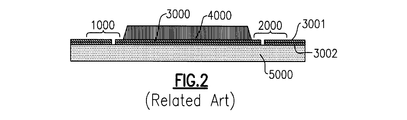
- FIGS. 1 and 2 illustrate an example of a conventional acoustic wave element 6000, which may be used in an electronic device such as a wireless communication apparatus.
- FIG. 1 shows a plan view of the conventional acoustic wave element 6000
- FIG. 2 shows a corresponding cross-sectional view taken along line B-BB of FIG. 1.
- the conventional acoustic wave element 6000 includes a first interdigital transducer (IDT) electrode 1000 and a second IDT electrode 2000 both provided on the upper surface of a piezoelectric body 5000.
- IDT interdigital transducer
- the conventional acoustic wave element 6000 further includes a connection wiring 3000 connecting the first IDT electrode 1000 to the second IDT electrode 2000, and a reinforcement electrode 4000 provided on the connection wiring 3000.
- the reinforcement electrode 4000 is provided for reducing the electric resistance of the connection wiring 3000 connecting the first IDT electrode 1000 to the second IDT electrode 2000.
- the connection wiring 3000 includes a lower connection wiring 3002 and an upper connection wiring 3001.
- the upper connection wiring 3001 is provided on the upper surface of the lower connection wiring 3002.
- Japanese Patent Application Publication No. 2011-71912 describes an example of such a conventional acoustic wave element.
- aspects and embodiments are directed to an acoustic wave element and a ladder filter using the same.
- an acoustic wave element according to the present invention may be configured to greatly reduce the electric loss in the connection wiring electrically connected between the IDT electrodes, as discussed in more detail below.
- an acoustic wave element comprises a piezoelectric body having an upper surface, an interdigital transducer (IDT) electrode provided above the piezoelectric body, a connection wiring connected to the IDT electrode provided above the piezoelectric body, the connection wiring having a lower connection wiring and an upper connection wiring provided above the lower connection wiring, and a reinforcement electrode provided above the connection wiring, the reinforcement electrode being in contact with and electrically connected to the lower connection wiring.
- IDT interdigital transducer
- the connection wiring includes a hole electrode extending in a direction perpendicular to the upper surface of the piezoelectric body, the reinforcement electrode being electrically connected to the lower connection wiring via the hole electrode.
- the hole electrode extends through the upper connection wiring and the lower connection wiring, a first diameter of the hole electrode in the upper connection wiring being larger than a second diameter of the hole electrode in the lower connection wiring.
- the material of the lower connection wiring may be different from the material of the upper connection wiring.
- an oxygen affinity of the material of the lower connection wiring may be less than an oxygen affinity of the material of the upper connection wiring.
- the reinforcement electrode may be in contact with and electrically connected to an upper surface of the lower connection wiring.
- the upper connection wiring is divided by the reinforcement electrode in a cross section taken in a direction perpendicular to the upper surface of the piezoelectric body to provide first and second upper connection wirings, the first and second upper connection wirings being electrically connected to each other via the reinforcement electrode.
- the acoustic wave element may further comprise a third connection electrode disposed on the piezoelectric body between the first and second upper connection wirings, the third connection wiring being covered with an insulation layer, and the reinforcement electrode extending over the insulation layer.
- the lower connection wiring is divided by the reinforcement electrode in a cross section taken in the direction perpendicular to the upper surface of the piezoelectric body to provide first and second lower connection wirings, the first and second lower connection wirings being electrically connected to each other via the reinforcement electrode.
- the acoustic wave element may further comprise a third connection wiring disposed on the piezoelectric body between the first and second lower connection wirings, the third connection wiring being covered with an insulation layer, and the reinforcement electrode extending over the insulation layer.
- the IDT electrode includes a lower IDT electrode and an upper IDT electrode provided above the lower IDT electrode, a material of the lower IDT electrode being identical to a material of the lower connection wiring, and a material of the upper IDT electrode being identical to a material of the upper connection wiring.
- an acoustic wave element comprises a piezoelectric body having an upper surface, a first interdigital transducer (IDT) electrode disposed on the piezoelectric body, a second IDT electrode disposed on the piezoelectric body, a connection wiring disposed on the upper surface of the piezoelectric body and electrically connected to the first IDT electrode and the second IDT electrode, the connection wiring including a lower connection wiring and a upper connection wiring disposed above the lower connection wiring, and a reinforcement electrode disposed above the connection wiring, the reinforcement electrode being in contact with and electrically connected to the lower connection wiring.
- IDT interdigital transducer
- the lower connection wiring is formed of a first material and the upper connection wiring is formed of a second material, an oxygen affinity of the first material being less than an oxygen affinity of the second material.
- the reinforcement electrode is further in contact with and electrically connected to the upper connection wiring.
- the connection wiring may further include a hole electrode extending through the upper connection wiring and the lower connection wiring in a direction perpendicular to the upper surface of the piezoelectric body.
- the hole electrode has a first diameter in the upper connection wiring and a second diameter in the lower connection wiring, the first diameter being larger than the second diameter.
- the reinforcement electrode is electrically connected to the lower connection wiring via the hole electrode.
- connection wiring including both the upper and lower connection wirings, is divided by the reinforcement electrode in a cross section taken in a direction perpendicular to the upper surface of the piezoelectric body to provide first and second connection wirings, the first and second connection wirings being electrically connected to each other via the reinforcement electrode.
- the acoustic wave element may further comprise a third connection wiring disposed on the piezoelectric body between the first and second connection wirings, the third connection wiring being covered with an insulation layer, and the reinforcement electrode extending over the insulation layer.
- Another embodiment is directed to a ladder filter including the acoustic wave element of any of the examples discussed above.
- an acoustic wave element comprises a piezoelectric body having an upper surface, a first interdigital transducer (IDT) electrode disposed on the piezoelectric body, a second IDT electrode disposed on the piezoelectric body, a connection wiring disposed on the upper surface of the piezoelectric body and electrically connected to the first IDT electrode and the second IDT electrode, and means for reducing electric loss in the connection wiring.
- IDT interdigital transducer
- FIG. 1 is a plan view schematically showing an example of a conventional acoustic wave element
- FIG. 2 is a cross-sectional view of the conventional acoustic wave element of FIG. 1 taken along line B-BB in FIG. 1
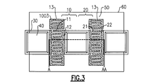
- FIG. 3 is a plan view schematically showing one example of an acoustic wave element according to aspects of the present invention
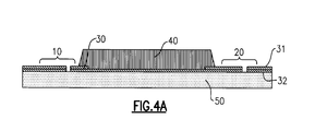
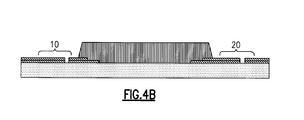
- FIGS. 4A-D are cross-sectional views of examples of the acoustic wave element of FIG. 3 taken along line A-AA in FIG. 3
- FIGS. 4A-D are cross-sectional views of examples of the acoustic wave element of FIG. 3 taken along line A-AA in FIG. 3
- FIGS. 4A-D are cross-sectional views of examples of the acoustic wave element of FIG. 3 taken along line A-AA in FIG. 3
- FIGS. 4A-D are cross-sectional views of examples of the acoustic wave element of FIG. 3 taken along line A-AA in FIG. 3;
- FIGS. 4A-D are cross-sectional views of examples of the acoustic wave element of FIG. 3 taken along line A-AA in FIG. 3;
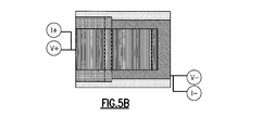
- FIG. 5A is a cross-sectional view of one example of a conventional acoustic wave element showing measurement conditions of a contact resistance value of the connection wiring;
- FIG. 5B is a corresponding plan view of the example conventional acoustic wave element of FIG. 5A;
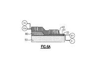
- FIG. 6A is a cross-sectional view of one example of an acoustic wave element showing measurement conditions of a contact resistance value of the connection wiring according to aspects of the present invention;
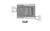
- FIG. 6B is a corresponding plan view of the example acoustic wave element of FIG. 6A;
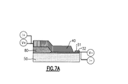
- FIG. 7A is a cross-sectional view of another example of an acoustic wave element showing measurement conditions of a contact resistance value of the connection wiring according to aspects of the present invention;
- FIG. 7B is a corresponding plan view of the example acoustic wave element of FIG. 7A;
- FIG. 8 is a characteristic diagram showing measurement results of the contact resistance value of the connection wiring corresponding to the examples of FIGS. 5A-7B;
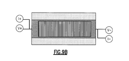
- FIG. 9A is a cross-sectional view of an example of a conventional acoustic wave element showing measurement conditions of a resistance value per unit length of the connection wiring;
- FIG. 9A is a cross-sectional view of an example of a conventional acoustic wave element showing measurement conditions of a resistance value per unit length of the connection wiring;
- FIG. 9B is a corresponding plan view of the example conventional acoustic wave element of FIG. 9A;
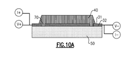
- FIG. 10A is a cross-sectional view of one example of an acoustic wave element showing measurement conditions of a resistance value per unit length of the connection wiring, according to aspects of the present invention;
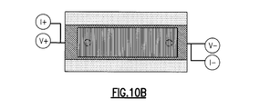
- FIG. 10B is a corresponding plan view of the example acoustic wave element of FIG. 10A;
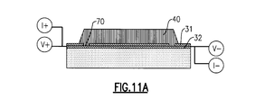
- FIG. 11A is a cross-sectional view of another example of an acoustic wave element showing measurement conditions of a resistance value per unit length of the connection wiring, according to aspects of the present invention;
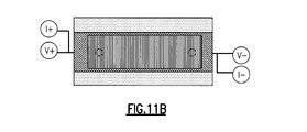
- FIG. 11B is a corresponding plan view of the example acoustic wave element of FIG. 11A;
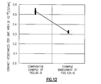
- FIG. 12 is a characteristic diagram showing measurement results of the resistance value of the connection wiring corresponding to the examples of FIGS. 9A-11B;
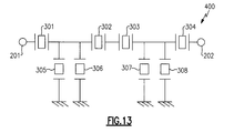
- FIG. 13 is a circuit diagram of one example of a ladder filter according to aspects of the present invention; and
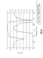
- FIG. 14 is a characteristic diagram showing passing characteristics of the ladder filter according to aspects of the present invention.
- FIG. 3 is a plan view schematically illustrating an embodiment of the acoustic wave element 60.
- FIGS. 4A-D are cross-sectional views of various examples of the acoustic wave element 60 taken along line A-AA in FIG. 3.
- the acoustic wave element 60 includes a piezoelectric body 50 made of a single crystal piezoelectric material. A first IDT electrode 10 and a second IDT electrode 20 are provided on the upper surface of the piezoelectric body 50.
- the acoustic wave element 60 further includes two reflectors 13 disposed adjacent the IDT electrodes 10, 20 in the propagation direction of an acoustic wave generated by the first IDT electrode 10 and the second IDT electrode 20.
- the acoustic wave element 60 further includes a connection wiring 30 electrically connecting the first IDT electrode 10 and the second IDT electrode 20, and a reinforcement electrode 40 provided on the upper surface of the connection wiring 30 for reducing the electric loss of the connection wiring 30.
- the first IDT electrode 10 has comb-shaped electrodes each including a line-shaped first bus bar 12 and a plurality of first electrode fingers 11 perpendicularly extending with respect to the line direction of the line-shaped first bus bar 12.
- the first IDT electrode 10 is made of the opposing comb-shaped electrodes.
- the second IDT electrode 20 includes comb-shaped electrodes each having a second bus bar 22 and a plurality of second electrode fingers 21.
- the first IDT electrode 10, the second IDT electrode 20, the reflectors 13, the connection wiring 30, and the reinforcement electrode 40 may be formed by patterning a metallic thin film.
- the acoustic wave element 60 may be improved in its temperature characteristic by providing a dielectric layer that covers the upper surfaces of the piezoelectric body 50, the first IDT electrode 10, the second IDT electrode 20, the reflectors 13, the connection wiring 30, and the reinforcement electrode 40.
- connection wiring 30 includes an upper connection wiring 31 and a lower connection wiring 32.
- the lower connection wiring 32 and the reinforcement electrode 40 are in contact with and electrically connected to each other so that the electric loss can be greatly reduced in the connection wiring 30.
- the electric loss may occur when an oxide film formed on the surface of the upper connection wiring 31 and the lower connection wiring 32 during the thin film processing blocks the electrical connection between the connection wiring 30 and the reinforcement electrode 40.
- the electrical resistance reduction effect of the connection wiring 30, which is effected by providing the reinforcement electrode 40 as described above may be lost or degraded by the presence of the oxide film.
- certain aspects and embodiments address the oxide film formed on the surface of the connection wiring 30 and reduce the electric loss in the connection wiring 30 by reducing the contact resistance between the connection wiring 30 and the reinforcement electrode 40.
- the material forming the upper connection wiring 31 and the lower connection wiring 32 may preferably be a material that is not likely to form an oxide film on the surface.
- the susceptibility to oxidation is represented by an oxygen affinity.
- the main cause of the electric loss reduction effect in the connection wiring 30 in one embodiment is the configuration in which the lower connection wiring 32 and the reinforcement electrode 40 are in contact with and electrically connected to each other, it may be preferable to allow the oxygen affinity of the material forming the lower connection wiring 32 to be less than the oxygen affinity of the material forming the upper connection wiring 31.
- the oxygen affinity of the material generally correlates with a standard free-energy, and the less the standard free-energy (Delta G/kJmol -1 ), the less the oxygen affinity. Representative materials are exemplified by: listed in ascending order of the standard free-energy.
- connection wiring 31 and the lower connection wiring 32 are described in at least one embodiment, the structure is not limited to two layers and may be configured as three or more layers.
- connection wiring 30 and the reinforcement electrode 40 are described in detail below with reference to FIGS. 4A-D.
- connection wiring 32 and the reinforcement electrode 40 are in contact with and electrically connected to each other in the connection wiring 30.
- the lower connection wiring 32, the upper connection wiring 31, and the reinforcement electrode 40 are sequentially provided on the upper surface of the piezoelectric body 50.
- the connection wiring 30 can be integrally and simultaneously formed with the first IDT electrode 10 and the second IDT electrode 20 using thin film processing.
- the upper connection wiring 31 is divided by the reinforcement electrode 40, and the upper surface of the lower connection wiring 32 and the reinforcement electrode 40 are in contact with and electrically connected to each other.
- the upper surface and the side surfaces of the upper connection wiring 31 are in contact with and electrically connected to the reinforcement electrode 40.
- the lower connection wiring 32 is also divided by the reinforcement electrode 40, and the piezoelectric body 50 also has a surface in contact with the reinforcement electrode 40.
- the reinforcement electrode 40 may be characterized by the configuration of being in contact with and electrically connected to the side surfaces of the lower connection wiring 32.
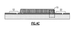
- a hole electrode 70 is provided extending in the direction perpendicular to the upper surface of the piezoelectric body 50 through the upper connection wiring 31 and the lower connection wiring 32, such that the lower connection wiring 32 and the reinforcement electrode 40 are in contact with and electrically connected to each other.
- the cross-sectional area of the hole electrode 70 provided in the lower connection wiring 32 it may be preferable to allow the cross-sectional area of the hole electrode 70 provided in the lower connection wiring 32 to be less than the cross-sectional area of the hole electrode 70 provided in the upper connection wiring 31, such that not only the side surfaces of the lower connection wiring 32 but also the upper surface thereof can be in contact with and electrically connected to the reinforcement electrode 40.
- the contact area is greater to further reduce the contact resistance.
- the shape of the hole electrode 70 is not limited to the example shown in FIG. 4C, and may have any cross-sectional shape, including, for example, circular, rectangular, and the like.
- the cross section may be differently configured in the depth direction of the hole electrode 70.
- the hole electrode 70 may be provided only in the upper connection wiring 31 for the upper surface of the lower connection wiring 32 to be in contact with and electrically connected to the hole electrode 70.
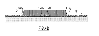
- connection wiring 120 is illustrated another configuration of the connection wiring according to certain examples.
- one connection wiring 30 divided by the reinforcement electrode 40 is designated as a first connection wiring 100 and the other connection wiring 30 is designated as a second connection wiring 110
- a third connection wiring 120 is provided on the upper surface of the piezoelectric body 50 between the first connection wiring 100 and the second connection wiring 110.
- the third connection wiring 120 is covered with an insulation layer 80.
- the reinforcement electrode 40 may cross with an overpass of the third connection wiring 120 via the insulation layer 80, and the first connection wiring 100 and the second connection wiring 110 are in contact with and electrically connected to each other.
- the third connection wiring 120 may be an electrode that has a potential different from that of the first connection wiring 100 or the second connection wiring 110.
- the third connection wiring 120 may be integrally and simultaneously formed with the first connection wiring 100 and the second connection wiring 110. It may be preferable to adopt the same configuration (e.g., a vertically two-layer structure) and the same material for simplifying the manufacturing process.
- connection wiring 30 and the reinforcement electrode 40 will be described below, comparing embodiments of acoustic wave element 60 with a conventional acoustic wave element, and with reference to FIGS. 5A-7B, which illustrate examples of measuring the contact resistances in the connection wiring 30 and the reinforcement electrode 40.
- FIG. 5A is a cross-sectional view and FIG. 5B is a plan view corresponding to the configuration of the conventional acoustic wave element of FIG. 2.
- FIGS. 5A and 5B illustrate a comparative example in which the reinforcement electrode 40 is only in contact with and electrically connected to the upper connection wiring 31.
- FIGS. 6A and 6B illustrate a cross-sectional view and corresponding plan view, respectively, of one example of an embodiment of the acoustic wave element 60 in which the upper connection wiring 31 and the lower connection wiring 32 are in contact with and electrically connected to each other.
- FIGS. 7A and 7B illustrate a cross-sectional view and corresponding plan view, respectively, of another example of an embodiment of the acoustic wave element 60 in which only the lower connection wiring 32 is in contact with and electrically connected to the reinforcement electrode 40.
- the reinforcement electrode 40 is made of Aluminum (Al)
- the upper connection wiring 31 is made of an Aluminum alloy
- the lower connection wiring 32 is made of Molybdenum (Mo)
- the total contact area between the reinforcement electrode 40 and the connection wiring 30 is 400 um 2 .
- FIG. 8 shows the measurement results of the contact resistance per unit area between the connection wiring 30 and the reinforcement electrode 40.
- Five measurement points are plotted per each of FIGS. 5A-7B in FIG. 8.
- the contact resistances per unit area of the embodiments of FIGS. 6A-B and 7A-B are lower than the contact resistances per unit area of the comparative example of FIGS. 5A-B. This is because the oxide film formed on the upper surface of the upper connection wiring 31 during the thin film processing increases the contact resistances per unit area between the reinforcement electrode 40 and the connection wiring 30.
- the contact resistances per unit area of the embodiment of FIGS. 7A-B are lower than the contact resistances per unit area of the embodiments of FIGS. 5A-B and 6A-B.
- connection wiring 30 configuring the connection wiring 30 according to certain embodiments such that at least the lower connection wiring 32 is in contact with and electrically connected to the reinforcement electrode 40 reduces the contact resistance between the connection wiring 30 and the reinforcement electrode 40. As a result, the electric loss in the connection wiring 30 can be reduced.
- connection wiring 30 Examples of the resistance values per unit length of the connection wiring 30 will be described below, comparing another embodiment of the acoustic wave element 60 with a conventional acoustic wave element, and with reference to FIGS. 9A-11B, which illustrate examples of measuring the resistance values per unit length of the connection wiring 30.
- the connection wiring configuration and the structure material of each configuration are similar to the configuration described above and illustrated in FIG. 4.
- the lower connection wiring 32 is provided on the upper surface of piezoelectric body 50, and the reinforcement electrode 40 is subsequently provided on the upper surface of lower connection wiring 32.
- FIGS. 9A and 9B illustrate a cross-sectional view and corresponding plan view, respectively, of a comparative example in which there is no contact between the reinforcement electrode 40 and the lower connection wiring 32.
- the cross-sectional view of FIG. 10A and the corresponding plan view of FIG. 10B show an example embodiment in which the hole electrode 70 has a diameter of 8 um and extends through the upper connection wiring 31 and the lower connection wiring 32.
- the hole electrode 70 is filled with the reinforcement electrode 40, with the reinforcement electrode 40 and the side surfaces of the lower connection wiring 32 being electrically connected to each other via the hole electrode 70.
- FIG. 12 shows measurement results of the resistance values per unit length of the connection wiring 30.
- the resistance values per unit length in the connection wiring 30 of the example embodiment illustrated in FIGS. 10A-B are lower than the resistance values per unit length in the connection wiring 30 of the comparative example illustrated in FIGS. 9A-B.
- the lower connection wiring 32 and the reinforcement electrode 40 may be in contact with and electrically connected to each other even by a small area, and the result is that the electric loss may be reduced in the connection wiring 30.
- FIGS. 11A and 11B illustrate cross-section and plan views, respectively, of another configuration in which the hole electrode 70 is filled with the reinforcement electrode 40 and is provided only in the upper connection wiring 31 for the reinforcement electrode 40 to be in contact with and electrically connected to the upper surface of the lower connection wiring 32.
- This configuration may also reduce the resistance value per unit length of the connection wiring 30 with respect to the comparative example of FIGS. 9A-B, and may also achieve the reduction effect of the electric loss in the connection wiring 30.
- the diameter of the hole electrode 70 is not limited to the example of 8 um discussed above, and that the effect of the reducing electric loss may be achieved by the lower connection wiring 32 and the reinforcement electrode 40 being in contact with and electrically connected to each other.
- FIG. 13 is a circuit diagram of one example of a ladder filter 400 using an embodiment of the acoustic wave element 60.
- the ladder filter 400 according to one embodiment includes a first serial resonator 301, a second serial resonator 302, a third serial resonator 303, and a fourth serial resonator 304 serially connected between an input terminal 201 and an output terminal 202.
- a first parallel resonator 305 and a second parallel resonator 306 are connected at one end between the first serial resonator 301 and the second serial resonator 302 and connected at the other end to the ground.
- a third parallel resonator 307 and a fourth parallel resonator 308 are connected at one end between the third serial resonator 303 and the fourth serial resonator 304 and connected at the other end to the ground.
- Each of the resonators 301, 302, 303, 304, 305, 306, 307, and 308 may include the acoustic wave element 60.
- both ends of each of the IDT electrodes of the resonators of the ladder filter 400 are provided at a single portion with the hole electrode 70, as shown in FIG. 10B, whereas the comparative example is manufactured having no hole electrode 70.
- the passing characteristics for each ladder filter are compared in FIG. 14.
- FIG. 14 shows measurement results of the passing characteristics in the ladder filter 400.
- the ladder filter of the example embodiment may enhance the attenuation amount in the passband and may reduce the minimum insertion loss in the passband with respect to that of the comparative example.
- Embodiments of the acoustic wave element discussed herein are useful in configurations of a ladder filter and/or in various electronic devices, such as a cell phone.
Landscapes
- Physics & Mathematics (AREA)
- Acoustics & Sound (AREA)
- Engineering & Computer Science (AREA)
- Chemical & Material Sciences (AREA)
- Crystallography & Structural Chemistry (AREA)
- Power Engineering (AREA)
- Manufacturing & Machinery (AREA)
- Surface Acoustic Wave Elements And Circuit Networks Thereof (AREA)
Priority Applications (5)
| Application Number | Priority Date | Filing Date | Title |
|---|---|---|---|
| CN201580008819.5A CN106031031B (zh) | 2014-02-18 | 2015-02-17 | 声波元件和使用声波元件的梯型滤波器 |
| KR1020167025532A KR20160124175A (ko) | 2014-02-18 | 2015-02-17 | 탄성파 소자 및 이것을 이용한 래더 필터 |
| JP2016569125A JP6342017B2 (ja) | 2014-02-18 | 2015-02-17 | 弾性波素子とこれを用いたラダーフィルタ |
| US14/624,993 US9614495B2 (en) | 2014-02-18 | 2015-02-18 | Elastic wave element with a reinforcement electrode and ladder filter using same |
| US15/438,402 US10389326B2 (en) | 2014-02-18 | 2017-02-21 | Methods of reducing electric loss in elastic wave elements |
Applications Claiming Priority (2)
| Application Number | Priority Date | Filing Date | Title |
|---|---|---|---|
| JP2014-028059 | 2014-02-18 | ||
| JP2014028059 | 2014-02-18 |
Related Child Applications (1)
| Application Number | Title | Priority Date | Filing Date |
|---|---|---|---|
| US14/624,993 Continuation US9614495B2 (en) | 2014-02-18 | 2015-02-18 | Elastic wave element with a reinforcement electrode and ladder filter using same |
Publications (1)
| Publication Number | Publication Date |
|---|---|
| WO2015125460A1 true WO2015125460A1 (en) | 2015-08-27 |
Family
ID=52706226
Family Applications (1)
| Application Number | Title | Priority Date | Filing Date |
|---|---|---|---|
| PCT/JP2015/000718 Ceased WO2015125460A1 (en) | 2014-02-18 | 2015-02-17 | Acoustic wave elements and ladder filters using same |
Country Status (5)
| Country | Link |
|---|---|
| US (2) | US9614495B2 (enExample) |
| JP (2) | JP6342017B2 (enExample) |
| KR (1) | KR20160124175A (enExample) |
| CN (1) | CN106031031B (enExample) |
| WO (1) | WO2015125460A1 (enExample) |
Families Citing this family (3)
| Publication number | Priority date | Publication date | Assignee | Title |
|---|---|---|---|---|
| CN107852148B (zh) * | 2015-08-31 | 2021-05-25 | 京瓷株式会社 | 声表面波元件 |
| US11463037B2 (en) * | 2020-09-10 | 2022-10-04 | Delta Electronics, Inc. | Motor control system and method of controlling the same |
| US20230179171A1 (en) | 2021-12-06 | 2023-06-08 | Skyworks Solutions, Inc. | Multi-band surface acoustic wave filters |
Citations (7)
| Publication number | Priority date | Publication date | Assignee | Title |
|---|---|---|---|---|
| EP0702379A1 (en) * | 1994-09-16 | 1996-03-20 | Kabushiki Kaisha Toshiba | Electronic and/or magnetic devices |
| US20020121841A1 (en) * | 2000-12-26 | 2002-09-05 | Murata Manufacturing Co., Ltd. | Surface acoustic wave apparatus and manufacturing method therefor |
| EP1274167A2 (en) * | 2001-07-06 | 2003-01-08 | Murata Manufacturing Co., Ltd. | Surface acoustic wave element and manufacturing method of the same |
| EP2175556A1 (en) * | 2007-07-30 | 2010-04-14 | Murata Manufacturing Co. Ltd. | Elastic wave device and method for manufacturing the same |
| US20100148890A1 (en) * | 2007-10-30 | 2010-06-17 | Fujitsu Limited | Acoustic wave element, duplexer, communication module, and communication apparatus |
| JP2011071912A (ja) | 2009-09-28 | 2011-04-07 | Taiyo Yuden Co Ltd | 弾性波フィルタ |
| US20130234558A1 (en) * | 2010-11-10 | 2013-09-12 | Murata Manufacturing Co., Ltd. | Acoustic wave device and method for manufacturing the same |
Family Cites Families (17)
| Publication number | Priority date | Publication date | Assignee | Title |
|---|---|---|---|---|
| US5003579A (en) * | 1986-08-22 | 1991-03-26 | Farallon Computing, Incorporated | System for connecting computers via telephone lines |
| US5338575A (en) * | 1990-01-10 | 1994-08-16 | Kohiensaure-werke Rud. Buse GmbH & Co. | Process for the quasi-continuous decaffeination of raw coffee |
| JPH1022767A (ja) * | 1996-07-09 | 1998-01-23 | Oki Electric Ind Co Ltd | 表面弾性波フィルタ及びその製造方法 |
| US7612470B2 (en) * | 1999-01-12 | 2009-11-03 | Microsemi Corp.—Analog Mixed Signal Group Ltd. | System for providing power over Ethernet through a patch panel |
| US7376734B2 (en) * | 2002-02-14 | 2008-05-20 | Panduit Corp. | VOIP telephone location system |
| JP2004129238A (ja) * | 2002-09-10 | 2004-04-22 | Matsushita Electric Ind Co Ltd | 帯域阻止型フィルタ、フィルタ装置、アンテナ共用器、通信機器 |
| JP3764450B2 (ja) * | 2003-07-28 | 2006-04-05 | Tdk株式会社 | 表面弾性波素子、表面弾性波装置、表面弾性波デュプレクサ、及び表面弾性波素子の製造方法 |
| JP2006074223A (ja) * | 2004-08-31 | 2006-03-16 | Murata Mfg Co Ltd | 電子部品およびその製造方法 |
| JP5023749B2 (ja) * | 2007-03-16 | 2012-09-12 | パナソニック株式会社 | 弾性表面波フィルタ |
| US8401387B2 (en) * | 2007-08-30 | 2013-03-19 | Calix, Inc. | Optical network interface devices and methods |
| JP2011030208A (ja) * | 2009-07-03 | 2011-02-10 | Panasonic Corp | 弾性波フィルタ及びこれを用いたデュプレクサ |
| US8334737B2 (en) * | 2009-07-15 | 2012-12-18 | Panasonic Corporation | Acoustic wave device and electronic apparatus using the same |
| JP5338575B2 (ja) * | 2009-09-03 | 2013-11-13 | パナソニック株式会社 | 弾性波素子とこれを用いた電子機器 |
| US9099981B2 (en) * | 2010-01-20 | 2015-08-04 | Skyworks Panasonic Filter Solutions Japan Co., Ltd. | Acoustic wave device having an inorganic insulator and an organic insulator |
| US8935543B2 (en) * | 2010-04-02 | 2015-01-13 | Andrew Llc | Method and apparatus for distributing power over communication cabling |
| JP5402841B2 (ja) * | 2010-06-14 | 2014-01-29 | 株式会社村田製作所 | 弾性表面波デバイス |
| DE112011103586B4 (de) * | 2010-10-26 | 2017-05-18 | Murata Manufacturing Co., Ltd. | Demultiplexer für elastische Wellen |
-
2015
- 2015-02-17 WO PCT/JP2015/000718 patent/WO2015125460A1/en not_active Ceased
- 2015-02-17 CN CN201580008819.5A patent/CN106031031B/zh active Active
- 2015-02-17 KR KR1020167025532A patent/KR20160124175A/ko not_active Withdrawn
- 2015-02-17 JP JP2016569125A patent/JP6342017B2/ja active Active
- 2015-02-18 US US14/624,993 patent/US9614495B2/en active Active
-
2017
- 2017-02-21 US US15/438,402 patent/US10389326B2/en active Active
-
2018
- 2018-05-15 JP JP2018093592A patent/JP6513262B2/ja active Active
Patent Citations (7)
| Publication number | Priority date | Publication date | Assignee | Title |
|---|---|---|---|---|
| EP0702379A1 (en) * | 1994-09-16 | 1996-03-20 | Kabushiki Kaisha Toshiba | Electronic and/or magnetic devices |
| US20020121841A1 (en) * | 2000-12-26 | 2002-09-05 | Murata Manufacturing Co., Ltd. | Surface acoustic wave apparatus and manufacturing method therefor |
| EP1274167A2 (en) * | 2001-07-06 | 2003-01-08 | Murata Manufacturing Co., Ltd. | Surface acoustic wave element and manufacturing method of the same |
| EP2175556A1 (en) * | 2007-07-30 | 2010-04-14 | Murata Manufacturing Co. Ltd. | Elastic wave device and method for manufacturing the same |
| US20100148890A1 (en) * | 2007-10-30 | 2010-06-17 | Fujitsu Limited | Acoustic wave element, duplexer, communication module, and communication apparatus |
| JP2011071912A (ja) | 2009-09-28 | 2011-04-07 | Taiyo Yuden Co Ltd | 弾性波フィルタ |
| US20130234558A1 (en) * | 2010-11-10 | 2013-09-12 | Murata Manufacturing Co., Ltd. | Acoustic wave device and method for manufacturing the same |
Also Published As
| Publication number | Publication date |
|---|---|
| JP6342017B2 (ja) | 2018-06-13 |
| JP6513262B2 (ja) | 2019-05-15 |
| JP2017506866A (ja) | 2017-03-09 |
| US20150236238A1 (en) | 2015-08-20 |
| US10389326B2 (en) | 2019-08-20 |
| US9614495B2 (en) | 2017-04-04 |
| CN106031031A (zh) | 2016-10-12 |
| US20170170797A1 (en) | 2017-06-15 |
| KR20160124175A (ko) | 2016-10-26 |
| CN106031031B (zh) | 2019-03-08 |
| JP2018170765A (ja) | 2018-11-01 |
Similar Documents
| Publication | Publication Date | Title |
|---|---|---|
| JP4798319B1 (ja) | 弾性波装置 | |
| JP6380558B2 (ja) | 弾性波装置 | |
| US9966929B2 (en) | Duplexer including a low-pass filter capacitor | |
| US10389326B2 (en) | Methods of reducing electric loss in elastic wave elements | |
| JP6465047B2 (ja) | 弾性波共振子、帯域通過型フィルタ及びデュプレクサ | |
| KR20200033960A (ko) | 탄성파 필터 장치 | |
| CN109845105A (zh) | 弹性波滤波器装置 | |
| US11309866B2 (en) | Acoustic wave device and method for manufacturing acoustic wave device | |
| CN105284049B (zh) | 滤波器装置以及双工器 | |
| CN110771040B (zh) | 弹性波滤波器装置、复合滤波器装置以及多工器 | |
| CN100511999C (zh) | 表面声波滤波器 | |
| KR101931679B1 (ko) | 래더형 필터 및 듀플렉서 | |
| CN114424457A (zh) | 弹性波装置 | |
| JP6981772B2 (ja) | 弾性波デバイス | |
| HK1229962A1 (en) | Acoustic wave elements and ladder filters using same | |
| JP2013243570A5 (enExample) | ||
| HK1229962B (zh) | 声波元件和使用声波元件的梯型滤波器 | |
| JP5852132B2 (ja) | 電子音響共振器 | |
| JP6784073B2 (ja) | 弾性表面波フィルタ | |
| JP6642385B2 (ja) | 弾性表面波フィルタ | |
| JP6620036B2 (ja) | 弾性波フィルタ、分波器および通信装置 | |
| WO2010038381A1 (ja) | 弾性波フィルタ装置 | |
| JP2012074169A (ja) | 複合電子部品 |
Legal Events
| Date | Code | Title | Description |
|---|---|---|---|
| 121 | Ep: the epo has been informed by wipo that ep was designated in this application |
Ref document number: 15711587 Country of ref document: EP Kind code of ref document: A1 |
|
| ENP | Entry into the national phase |
Ref document number: 2016569125 Country of ref document: JP Kind code of ref document: A |
|
| NENP | Non-entry into the national phase |
Ref country code: DE |
|
| ENP | Entry into the national phase |
Ref document number: 20167025532 Country of ref document: KR Kind code of ref document: A |
|
| 122 | Ep: pct application non-entry in european phase |
Ref document number: 15711587 Country of ref document: EP Kind code of ref document: A1 |