WO2015125366A1 - シリコンウェーハの製造方法およびシリコンウェーハ - Google Patents
シリコンウェーハの製造方法およびシリコンウェーハ Download PDFInfo
- Publication number
- WO2015125366A1 WO2015125366A1 PCT/JP2014/080632 JP2014080632W WO2015125366A1 WO 2015125366 A1 WO2015125366 A1 WO 2015125366A1 JP 2014080632 W JP2014080632 W JP 2014080632W WO 2015125366 A1 WO2015125366 A1 WO 2015125366A1
- Authority
- WO
- WIPO (PCT)
- Prior art keywords
- wire
- ingot
- silicon wafer
- cutting
- manufacturing
- Prior art date
- Legal status (The legal status is an assumption and is not a legal conclusion. Google has not performed a legal analysis and makes no representation as to the accuracy of the status listed.)
- Ceased
Links
Images









Classifications
-
- H—ELECTRICITY
- H10—SEMICONDUCTOR DEVICES; ELECTRIC SOLID-STATE DEVICES NOT OTHERWISE PROVIDED FOR
- H10P—GENERIC PROCESSES OR APPARATUS FOR THE MANUFACTURE OR TREATMENT OF DEVICES COVERED BY CLASS H10
- H10P54/00—Cutting or separating of wafers, substrates or parts of devices
-
- B—PERFORMING OPERATIONS; TRANSPORTING
- B23—MACHINE TOOLS; METAL-WORKING NOT OTHERWISE PROVIDED FOR
- B23D—PLANING; SLOTTING; SHEARING; BROACHING; SAWING; FILING; SCRAPING; LIKE OPERATIONS FOR WORKING METAL BY REMOVING MATERIAL, NOT OTHERWISE PROVIDED FOR
- B23D61/00—Tools for sawing machines or sawing devices; Clamping devices for these tools
- B23D61/18—Sawing tools of special type, e.g. wire saw strands, saw blades or saw wire equipped with diamonds or other abrasive particles in selected individual positions
- B23D61/185—Saw wires; Saw cables; Twisted saw strips
-
- B—PERFORMING OPERATIONS; TRANSPORTING
- B28—WORKING CEMENT, CLAY, OR STONE
- B28D—WORKING STONE OR STONE-LIKE MATERIALS
- B28D5/00—Fine working of gems, jewels, crystals, e.g. of semiconductor material; apparatus or devices therefor
- B28D5/04—Fine working of gems, jewels, crystals, e.g. of semiconductor material; apparatus or devices therefor by tools other than rotary type, e.g. reciprocating tools
- B28D5/045—Fine working of gems, jewels, crystals, e.g. of semiconductor material; apparatus or devices therefor by tools other than rotary type, e.g. reciprocating tools by cutting with wires or closed-loop blades
-
- H—ELECTRICITY
- H10—SEMICONDUCTOR DEVICES; ELECTRIC SOLID-STATE DEVICES NOT OTHERWISE PROVIDED FOR
- H10P—GENERIC PROCESSES OR APPARATUS FOR THE MANUFACTURE OR TREATMENT OF DEVICES COVERED BY CLASS H10
- H10P72/00—Handling or holding of wafers, substrates or devices during manufacture or treatment thereof
- H10P72/04—Apparatus for manufacture or treatment
- H10P72/0428—Apparatus for mechanical treatment or grinding or cutting
-
- H—ELECTRICITY
- H10—SEMICONDUCTOR DEVICES; ELECTRIC SOLID-STATE DEVICES NOT OTHERWISE PROVIDED FOR
- H10P—GENERIC PROCESSES OR APPARATUS FOR THE MANUFACTURE OR TREATMENT OF DEVICES COVERED BY CLASS H10
- H10P90/00—Preparation of wafers not covered by a single main group of this subclass, e.g. wafer reinforcement
Definitions
- the present invention relates to a silicon wafer manufacturing method and a silicon wafer.
- An epitaxial silicon wafer in which an epitaxial film is grown on a silicon wafer obtained by cutting a silicon single crystal ingot is known.
- warpage occurs when the resistance value in the silicon wafer and the resistance value in the epitaxial film are different. This is thought to be because elastic deformation occurs due to a lattice constant misfit between the silicon wafer and the epitaxial film.
- this warpage becomes large, there is a problem that mask alignment in the device manufacturing process, holding by a vacuum chuck, or the like becomes difficult.
- a wire saw using a wire is generally used.
- a wire saw wraps multiple wires between a plurality of main rollers, and presses a workpiece such as a semiconductor (hereinafter referred to as a workpiece) against the wire in a running state, thereby allowing the workpiece to be applied to a large number of plates having a predetermined thickness.
- Disconnect a workpiece such as a semiconductor (hereinafter referred to as a workpiece) against the wire in a running state, thereby allowing the workpiece to be applied to a large number of plates having a predetermined thickness.
- a free abrasive grain method for slicing with a wire saw This is a method of slicing the surface with a brass-plated steel wire while supplying a slurry in which abrasive grains such as GC (green silicon carbide) are mixed with oil-based or water-soluble oil or the like to a cutting site.
- abrasive grains such as GC (green silicon carbide) are mixed with oil-based or water-soluble oil or the like
- control parameters for controlling the shape of the obtained wafer there are many control parameters for controlling the shape of the obtained wafer.
- Typical examples include a flow rate (slurry flow rate) for supplying slurry (or coolant) to the processing portion, a speed at which a workpiece such as silicon is pressed against a wire in a running state (feed speed), and the like.
- Patent Document 3 proposes a silicon wafer manufacturing method for obtaining a silicon wafer having a desired warp by using a wire saw in which a wire is wound between a plurality of main rollers arranged at predetermined intervals. .
- the main rollers are displaced in the axial direction while the ingot is being cut. Due to the displacement of the main roller, the wire cutting the ingot moves in the axial direction of the ingot together with the main roller, and a desired warp corresponding to the amount of movement of the wire is formed on the surface of the silicon wafer obtained after the cutting.
- Patent Documents 1 and 2 there is no conventional method such as a step of predicting the warping direction after intentionally obtaining a silicon wafer from an ingot or a step of intentionally controlling the warping direction to a concave shape. There is a problem that a process is required. Further, in the configuration as described in Patent Document 3, it is necessary to displace the main roller in the axial direction during the cutting of the ingot, and there is a problem that the control of the wire saw becomes complicated.
- An object of the present invention is to provide a silicon wafer manufacturing method and a silicon wafer capable of obtaining a plurality of silicon wafers warped in a dome shape whose central portion is recessed in one direction with respect to an outer edge portion.
- the present inventor has a possibility of obtaining a plurality of silicon wafers warped in a dome shape whose central part is recessed in one direction by using a wire brazed as a wire saw wire. Focused on the fact that there is. Therefore, the present inventor conducted the following experiment.
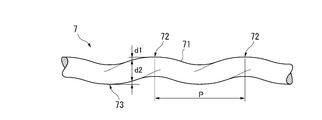
- the corrugated wire 7 is formed by brazing a wire 71 used for a normal straight wire in a spiral shape.
- the diameter of the wire 71 include 0.12 mm to 0.16 mm.
- brass plating carbon steel can be illustrated.
- the wavy wire 7 is brazed in a wave shape (substantially sinusoidal wave shape) when viewed from a direction orthogonal to the longitudinal direction thereof.
- the brazing pitch P (the interval between the highest points 72 adjacent to each other in FIG. 1A) is preferably 2.5 mm to 5.0 mm.
- the brazing displacement D ((the highest point 72 and the lowest point 73 and the distance d1 in FIG. 1A) ⁇ (the wire diameter d2 of the wire 71)) is preferably 6 ⁇ m to 12 ⁇ m.
- the advantage of the corrugated wire will be described.
- the wavy wire 7 can travel with the abrasive grains G1 entering between the adjacent highest points 72 or the adjacent lowest points 73. Therefore, it can be estimated that the abrasive grains G1 are sufficiently supplied also to the front side in the traveling direction (wire withdrawal side), and the front side machinability is improved as well as the rear side (wire entering side) machinability.
- the normal linear wire 9 does not have the portion where the abrasive grains G1 enter unlike the corrugated wire 7, and therefore the abrasive grains G1 are sufficiently supplied to the front side in the traveling direction. It can be estimated that the front side machinability is worse than the rear side machinability.
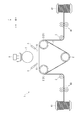
- the wire saw 1 includes a total of three main rollers 2 arranged on the same horizontal plane, two on the same horizontal plane and one below the middle of the two.
- a wave-like wire 7 is wound spirally along the axial direction (front-rear direction).
- Wire reels 41 and 42 are provided on both ends of the corrugated wire 7 to send out and wind the corrugated wire 7 through one guide roller 3 respectively.
- traversers 43 and 44 are provided between the guide rollers 3 and the wire reels 41 and 42, respectively.
- the traversers 43 and 44 have a function of adjusting the feeding position and the winding position of the wavy wire 7.
- nozzles 5 for supplying slurry-like abrasive liquid G to the intermediate positions of the two upper main rollers 21 are provided above the two upper main rollers 2 (hereinafter referred to as upper main rollers 21). It has been. Above the nozzle 5, a feeding means 6 that holds the ingot T and moves it up and down is provided.
- the wire saw 1 rotates the plurality of main rollers 2 to cause the wavy wire 7 to travel in a direction substantially orthogonal to the axial direction of the main roller 2 (left and right direction (hereinafter referred to as a wire traveling direction)).
- a wire traveling direction left and right direction
- the ingot T is lowered and pressed against the waved wire 7 that is running, whereby the ingot T is cut to manufacture a plurality of silicon wafers.
- the ingot T is lowered linearly in the direction of gravity with respect to the wavy wire 7 in order not to warp the silicon wafer.
- the cutting direction of the ingot T when it is not affected by the outside (hereinafter referred to as the cutting target direction) is the direction opposite to the gravity direction.
- the wavy wire 7 is linearly run in a direction substantially orthogonal to the axial direction of the ingot T.
- the traveling direction of the wavy wire 7 (hereinafter referred to as the “wire traveling target direction”) when not affected by the outside is linear.
- a case is considered where the wavy wire 7 is wound from the front to the back and in a left-handed spiral shape when viewed from the front.
- the wavy wire 7 travels in one direction parallel to the main roller 2 (hereinafter, the traveling direction at this time (the backward direction in the case shown in FIG. 2) is referred to as a wire traveling direction).
- the wavy wire 7 travels in one direction is, for example, not only a mode in which the wavy wire 7 is unilaterally fed from the wire reel 42 to the wire reel 41 but also a wavy wire that is fed from the wire reel 42 and wound by the wire reel 41.
- a mode in which the corrugated wire 7 travels in a reciprocating manner so that the length of the corrugated wire 7 is longer than the length of the corrugated wire 7 fed out from the wire reel 41 and wound up by the wire reel 42 is also provided. Including.
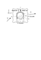
- the wavy wire 7 moves relatively from the lower part shown by the solid line and the broken line in FIG. 3A to the upper part shown by the two-dot chain line, and the ingot T is cut from the bottom to the top.
- the wire traveling direction is the backward direction in FIG. 2 and the wavy wire 7 travels leftward between the upper main rollers 21, the wavy wire 7 is shown in FIGS. 3B and 3C.
- the vehicle travels while turning leftward (twisting). In this case, at the turning entrance side T1, the abrasive grains G1 are sufficiently supplied, and the machinability is improved.
- the wavy wire 7 is brazed in a wavy shape, the wavy wire 7 travels in a state of being stretched substantially linearly because it travels in a state where tension is applied.
- the bending of the waved wire 7 becomes large.
- the supply of abrasive grains G1 to 7 is insufficient.
- a reduction in machinability due to the cutting powder T3 appears remarkably.
- the machinability on the turn-in side T1 is higher than that on the turn-out side T2, and the traveling direction of the corrugated wire 7 during cutting (hereinafter referred to as the cutting progress direction) is as shown in FIG. Tilt to the right.
- the cutting progress direction tilts to the right with respect to the cutting target direction
- the warp (hereinafter referred to as the warp in the cutting direction) is the center in the vertical direction (the center in the vertical direction in FIG. 3D) is the rear side in FIG. 2 (the right side in FIG. 3D). That is, it can be estimated that the arc shape is recessed in the wire traveling direction.
- the warpage in the cutting direction of the silicon wafer WF is an arc shape in which the central portion in the vertical direction is recessed toward the front side in FIG. 2, contrary to the state shown in FIG. 3D. Can be estimated.
- the wavy wire 7 is restricted from moving forward and backward by the inner wall of the groove of the main roller 2 (the degree of freedom is low).
- the movement restriction by the inner wall of the groove of the main roller 2 becomes gentle (higher degree of freedom) and is accompanied by the inclination in the cutting progress direction described above.
- the warp when the shape of the silicon wafer WF is measured in the traveling direction of the wavy wire 7 (hereinafter referred to as the warping in the traveling direction) is the center in the left-right direction (the vertical direction in FIG. 4B).
- the central portion has an arc shape that is recessed toward the rear side in FIG.
- the warpage in the traveling direction of the silicon wafer WF is opposite to the state shown in FIG. 4B, and the vertical center is the front side in FIG. 2 (left side in FIG. 4B).
- the arc shape is recessed in the shape of a circle. From the above, a plurality of silicon wafers WF warped in a dome shape whose central portion is recessed in one direction (wire traveling direction) can be obtained by cutting the ingot T using the wavy wire 7 brazed in a wave shape. Estimated possible.
- a straight wire means a straight wire that is not brazed in a predetermined shape such as a wave shape or a spiral shape.
- Each wire was wound around the main roller 2 in the state described in the above hypothesis. Further, when the wire traveling direction is set to the forward direction, the wavy wire 7 travels between the upper main rollers 21 in the right direction in the configuration in which the wavy wire 7 is wound around the main roller 2 in the same manner as the hypothesis described above. Thus, the three main rollers 2 and the wire reels 41 and 42 were rotated. An ingot T having a diameter of 300 mm was used.
- the feed speed means the feed speed of the ingot when the ingot is pressed against the wire at the time of cutting the ingot (lowering speed in the case of the wire saw shown in FIG. 2).
- an initial cutting stage for example, when the wavy wire 7 is cutting the position indicated by the solid line in FIG. 3A
- a final cutting stage for example, the position indicated by the two-dot chain line in FIG. 3A.
- the contact portion between the ingot and the wire in the case of cutting is shorter than the contact portion in the middle stage of cutting (for example, when the wavy wire 7 is cutting the position indicated by the one-dot chain line in FIG. 3A). For this reason, the load which acts on a wire at the cutting
- the ingot cutting direction (in FIG. 2) was determined for the silicon wafers on the front side and the rear side of the ingot.
- the shape in the vertical direction) and the shape in the running direction of the wire were measured.
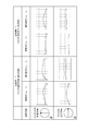
- the shapes shown in FIG. 5 and FIG. 6 below are the results of measurement using the surface located on the front side of the ingot as the upper surface.
- the substantially central portion is the same direction as the wire traveling direction (Experimental Example 1).
- silicon wafers prepared under the same conditions as in Experimental Example 1-2 were prepared as silicon wafers for Experimental Examples 2-1 and 2-2. Then, the silicon wafers of Experimental Examples 2-1 and 2-2 were ground under the condition that the machining allowance on both sides was 20 ⁇ m. The grinding was performed on each side. This is because if both sides are ground at the same time and the way they are cut is different, the silicon wafer will be warped due to the influence, and whether the warping after grinding is due to cutting or grinding. This is because we don't understand. A silicon wafer having a diameter of 300 mm was used.
- a plurality of warped dome shapes whose central portion is recessed in one direction with respect to the outer edge portion.
- a silicon wafer can be obtained.
- the wavy wire may be spirally brazed so that it looks like a circle when viewed from one end in the longitudinal direction, or straight when viewed from one end in the longitudinal direction. It may be simply wavyly brazed so that it can be seen.
- the warping in the running direction is an arc shape, but the warping in the cutting direction is not a smooth arc shape.
- the silicon wafer is preferably warped in a smooth arc shape. Therefore, the present inventor has paid attention to the possibility that a silicon wafer having a circular arc shape with a smooth warping in the cutting direction may be obtained by appropriately setting the feed speed as a result of extensive research. Therefore, the present inventor conducted the following experiment 3.
- the ingot was cut under the same conditions as in Experimental Example 1-2, and the relationship between the work amount W at that time and the warpage (shape) of the cutting direction of the silicon wafer was examined.
- the result is shown in FIG.
- the diameter of the silicon wafer is 300 mm.
- the feed rate at the middle stage of cutting is slower than the feed speed at the beginning and end of cutting.
- the rate of change of the work amount W is greatly different before and after the transition from the initial cutting stage to the middle cutting stage and before and after the transition from the middle cutting stage to the final cutting stage.
- the warping in the cutting direction is substantially arc shape. It can be estimated that the following silicon wafer is obtained. That is, it can be estimated that a silicon wafer having a circular arc shape with a smooth warping in the cutting direction can be obtained by controlling the feed speed so that the work amount W changes into a smooth curved line.
- a preferred embodiment of the present invention has been completed based on such findings.
- the cutting step is performed such that the feed speed of the ingot when the cylindrical ingot is pressed against the wavy wire is F, and the contact portion between the wavy wire and the ingot is
- the work amount W defined by the above formula (1) is maximum at the cutting position at which the diameter of the ingot is maximum with respect to the cutting position in the radial direction of the ingot in the cylindrical ingot. It is preferable to control the feed speed of the ingot so as to change to a substantially arc shape that is a value.
- the present invention it is possible to obtain a silicon wafer that warps in a dome shape as a whole with a simple arc shape in which the warping in the cutting direction becomes a smooth arc shape by simply controlling the feed speed of the ingot.
- a silicon wafer is manufactured with a linear wire, and the shape of the silicon wafer before and after the formation of the film is examined. It was. The results are shown in FIGS. 9A and 9B. As shown in FIGS. 9A and 9B, for both the cutting direction and the traveling direction, the warpage of the silicon wafer after the formation of the epitaxial film is about the center position where the diameter of the ingot (silicon wafer) is maximum. It was confirmed that the range of 50% (0.5 ⁇ R (diameter)) (hereinafter referred to as cutting center range A) was particularly large.
- the relationship between the cutting position of the cylindrical ingot and the length of the contact portion between the ingot and the wire is a quadratic curve shape (arc shape) that is maximum at the cutting position where the diameter of the ingot is maximum.
- the work amount W defined by the above formula (1) is proportional to the length of the contact portion between the ingot and the wire if the feed speed is substantially constant.
- the relationship between the cutting position and the work amount when the feed speed is constant is a quadratic curve having a maximum value at the center position of the ingot, as shown in FIG.
- the diameter of the ingot which shows a result in FIG. 11 is 300 mm.
- the cutting step includes Wmax as a work amount at a cutting position where the diameter of the ingot is maximum, and the ingot centered on a cutting position where the diameter of the ingot is maximum. It is preferable to control the feed speed of the ingot so as to satisfy the relationship represented by the above formula (2), where Wcnt is the work amount in a range of 50% of the diameter of the ingot.
- the cutting step is controlled so that the feed speed of the ingot is maintained substantially constant from the start of cutting of the ingot to the end of cutting.
- Example 5 An ingot having a diameter of 300 mm was cut under the same conditions as in Experiment 1-1 of Experiment 1 except that the tension was 10 N, 15 N, 25 N, and 30 N. As a result, it was confirmed that disconnection occurred when the tension was 10N and 30N, and no disconnection occurred when the tension was 15N and 25N. Moreover, Warp and Bow were calculated about the silicon wafer manufactured on the conditions whose tension
- FIG. 12A shows the calculation result of Warp
- FIG. 12B shows the calculation result of Bow.
- Warp and Bow are parameters representing the shape of the silicon wafer WF that is not attracted and fixed.
- a center plane in the thickness direction of the silicon wafer WF is used as the measurement plane CP, and a best fit plane of the measurement plane CP is used as the reference plane RP.
- Warp represents the maximum value of the deviation from the reference plane RP to the measurement plane CP.
- Bow represents a difference between the reference plane RP and the measurement plane CP at the center CT of the silicon wafer WF.
- the cutting step presses the ingot against the wavy wire whose tension is set to 15 N or more and 25 N or less.
- a silicon wafer can be manufactured without breaking the wavy wire.
- the silicon wafer of the present invention is manufactured by the above-described silicon wafer manufacturing method.
- FIG. 4 The figure which shows the shape of the cutting
- FIG. 4 The figure which shows the shape of the running direction before and after the epitaxial film formation of the silicon wafer which enlarged the curvature of the cutting center range in Experiment 4 forcibly.
- the ingot T is cut using a wire saw 1 as shown in FIG.
- the shape of the ingot T is not particularly limited, but is usually cylindrical.
- the diameter of the ingot T is not particularly limited, but is usually 100 mm to 450 mm.
- the corrugated wire 7 as a wire shown in FIG. 1A is spirally wound around the plurality of main rollers 2 of the wire saw 1.
- the direction in which the wavy wire 7 is wound may be left-handed or right-handed when viewed from the front.
- the traversers 43 and 44 are driven, and the plurality of main rollers 2 and the wire reels 41 and 42 are rotated, thereby causing the wavy wire 7 to travel in a direction substantially orthogonal to the axial direction of the main roller 2 (wire traveling).
- Step) While supplying the abrasive liquid G between the two upper main rollers 21, the ingot T is lowered and pressed against the traveling waved wire 7, thereby cutting the ingot T and separating the plurality of silicon wafers WF. Manufacture (cutting process).
- the wire traveling direction can be set according to the direction in which the silicon wafer WF is desired to be warped. That is, when it is desired to warp the silicon wafer WF in a dome shape recessed in the rear side in FIG. 2, the wire traveling direction may be set in the rear direction in FIG. What is necessary is just to set to the front direction in FIG.
- the feed speed can be set according to the shape of the warp in the cutting direction of the silicon wafer WF.
- the feed speed is set so that the work amount W defined by the above formula (1) changes to a substantially arc shape. It ’s fine.
- the feed speed may be set so that the work amount W becomes the maximum value at the cutting position where the diameter of the ingot T becomes the maximum. In this way, the feed speed may be changed depending on the cutting position so that the work amount W changes in a substantially arc shape, or the feed speed may be made substantially constant regardless of the cutting position.
- the feed speed may be controlled so that the work amount Wcnt in the cutting center range A satisfies the relationship of the above formula (2).
- the work amount at the lower end side end of the cutting center range A (a position moved by 25% of the diameter (R) from the center to the lower end side) Ab is Wb
- the upper end side end (center) When the work amount at At) (at a position moved by 25% of the diameter (R) to the upper end side) is Wt, the work amount Wb and the work amount Wt may be the same or different.
- the tension of the wavy wire 7 is 15N or more and 25N or less in order to prevent the wavy wire 7 from being disconnected.
- the silicon wafer WF can be manufactured without disconnecting the corrugated wire 7.
- the feed speed may be set so that the work amount W defined by the above formula (1) does not change in a substantially arc shape. Further, the feed speed may be controlled so that the work amount Wcnt of the cutting center range A does not satisfy the relationship of the above formula (2). Furthermore, a silicon wafer WF that warps in a dome shape may be manufactured using a wire that is not brazed in a wavy shape.
Landscapes
- Engineering & Computer Science (AREA)
- Mechanical Engineering (AREA)
- Finish Polishing, Edge Sharpening, And Grinding By Specific Grinding Devices (AREA)
- Processing Of Stones Or Stones Resemblance Materials (AREA)
- Mechanical Treatment Of Semiconductor (AREA)
Abstract
Description
エピタキシャルシリコンウェーハでは、シリコンウェーハにおける抵抗値と、エピタキシャル膜における抵抗値とが異なる場合、反りが発生することが知られている。この原因は、シリコンウェーハとエピタキシャル膜との格子定数のミスフィット(misfit)による弾性変形が生じるため、と考えられている。通常、この反りが大きくなると、デバイス製造工程におけるマスク合わせや、真空チャックによる保持等が困難となる不具合がある。
さらに、シリコンウェーハの研磨工程または研削工程において、シリコンウェーハの反り方向を故意に凹形状へ制御して、お椀状(ドーム状)にすることによりエピタキシャルシリコンウェーハの平坦度を向上させるエピタキシャルシリコンウェーハの製造方法が提案されている(例えば、特許文献2参照)。
この特許文献3では、互いに所定間隔をおいて配置された複数のメインローラ間にワイヤを巻回させたワイヤソーを用い、所望の反りを有するシリコンウェーハを得るシリコンウェーハの製造方法が提案されている。この製造方法では、インゴットを切断している間にそれぞれのメインローラを軸方向に変位させている。このメインローラの変位により、インゴットを切断しているワイヤがメインローラとともにインゴットの軸方向に移動し、切断後に得られるシリコンウェーハの表面に、そのワイヤの移動量に応じた所望の反りが形成される。
まず、波状ワイヤの構成について説明する。
図1Aに示すように、波状ワイヤ7は、通常の直線状のワイヤに用いる線材71を螺旋状に癖付けすることで形成されている。なお、線材71の直径としては、0.12mm~0.16mmが例示できる。また、線材71の材質としては、ブラスめっき炭素鋼が例示できる。
波状ワイヤ7は、その長手方向と直交する方向から見ると、波状(略正弦波状)に癖付けされている。癖付けのピッチP(図1Aにおける互いに隣り合う最高点72の間隔)は、2.5mm~5.0mmであることが好ましい。また、癖付けの変位D((図1Aにおける最高点72と最低点73と距離d1)-(線材71の線径d2))は、6μm~12μmであることが好ましい。
図1Bに示すように、波状ワイヤ7では、インゴットTを切断するときに、隣り合う最高点72の間や、隣り合う最低点73の間に砥粒G1が入り込んだ状態で走行することが可能であるため、走行方向の前方側(ワイヤ抜け側)にも砥粒G1が十分に供給され、当該前方側の切削性が後方側(ワイヤ入り側)の切削性と同じように良くなると推定できる。
これに対し、図1Cに示すように、通常の直線状のワイヤ9では、波状ワイヤ7のように砥粒G1が入り込む部分がないため、走行方向の前方側に砥粒G1が十分に供給されず、当該前方側の切削性が後方側の切削性より悪くなると推定できる。
次に、ワイヤソーの構成について説明する。
なお、以下において、図2の手前方向から観た場合を基準とし、方向を示した場合、「上」が+Z方向で「下(重力方向)」が-Z方向、「左」が+X方向で「右」が-X方向、「前」が-Y方向であって紙面に直交する手前方向で「後」が+Y方向であって奥方向とする。
図2に示すように、ワイヤソー1は、同一水平面上に2個、これら2個の中間の下方に1個配置された合計3個のメインローラ2を備えている。これら3個のメインローラ2の周りには、軸方向(前後方向)に沿って螺旋状に波状ワイヤ7が巻き付けられている。波状ワイヤ7の両端側には、それぞれ1個ずつのガイドローラ3を介して波状ワイヤ7を送り出したり巻き取ったりするワイヤリール41,42が設けられている。また、各ガイドローラ3とワイヤリール41,42との間には、それぞれトラバーサー43,44が設けられている。トラバーサー43,44は、波状ワイヤ7の送り位置、巻取り位置を調整する機能を有している。さらに、上側の2個のメインローラ2(以下、上側メインローラ21と称す)の上方には、2個の上側メインローラ21の中間位置にスラリー状の砥液Gを供給するノズル5がそれぞれ設けられている。また、ノズル5の上方には、インゴットTを保持して昇降させる送り手段6が設けられている。
ここで、通常、シリコンウェーハを反らせないために、インゴットTを波状ワイヤ7に対して重力方向に直線的に下降させる。このため、外部の影響を受けない場合のインゴットTの切断方向(以下、切断目標方向と称す)は、重力方向と反対方向となる。また、シリコンウェーハを反らせないために、波状ワイヤ7をインゴットTの軸方向に対して略直交する方向に直線的に走行させる。このため、外部の影響を受けない場合の波状ワイヤ7の走行方向(以下、ワイヤ走行目標方向と称す)は、直線的になる。
まず、以下のような仮説に基づく実験1を行った。
図2に示すワイヤソー1において、波状ワイヤ7を前から後ろに向けて、かつ、前から見て左巻きの螺旋状に巻き付けた場合を考える。このような状態で、波状ワイヤ7が上側メインローラ21間を左方向に走行するように、トラバーサ43,44を駆動するとともに、3個のメインローラ2とワイヤリール41,42とを回転させると、波状ワイヤ7は、メインローラ2と平行な一方向に進行する(以下、このときの進行方向(図2に示す場合にあっては後ろに向かう方向)を、ワイヤ進行方向と称す)。
なお、波状ワイヤ7が一方向に進行するとは、例えば、波状ワイヤ7をワイヤリール42からワイヤリール41に一方的に送り出す態様だけでなく、ワイヤリール42から送り出してワイヤリール41で巻き取る波状ワイヤ7の長さが、ワイヤリール41から送り出してワイヤリール42で巻き取る波状ワイヤ7の長さより長くなるように、波状ワイヤ7を往復に走行させて、波状ワイヤ7を一方向に進行させる態様も含む。
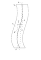
この切断の際、ワイヤ進行方向が図2における後ろ方向であって、波状ワイヤ7が上側メインローラ21間で左方向に走行する場合、波状ワイヤ7は、図3B,図3Cに示すように、メインローラ2に巻き付けられた軌跡に倣って、左方向に旋回しながら(ねじれながら)走行する。この場合、旋回入り側T1では、砥粒G1が潤沢に供給され、切削性が良くなる。一方、旋回出側T2では、インゴットTの切り粉T3によって目詰まりが起こり、切削性が悪くなる。
なお、波状ワイヤ7は、波状に癖付けされているが、張力が作用する状態で走行するため、略直線状に伸ばされた状態で走行する。
なお、ワイヤ進行方向を図2における前方向にした場合、シリコンウェーハWFの切断方向の反りは、図3Dに示す状態とは逆に、上下方向中央部が図2における前側に凹む円弧状になると推定できる。
その結果、図4Bに示すように、シリコンウェーハWFの形状を波状ワイヤ7の走行方向に測定した場合の反り(以下、走行方向の反りと称す)は、左右方向中央部(図4Bにおける上下方向中央部)が、図2における後ろ側(図4Bにおける右側)、すなわちワイヤ進行方向側に凹む円弧状になると推定できる。
なお、ワイヤ進行方向を図2における前方向にした場合、シリコンウェーハWFの走行方向の反りは、図4Bに示す状態とは逆に、上下方向中央部が図2における前側(図4Bにおける左側)に凹む円弧状になると推定できる。
以上のことから、波状に癖付けされた波状ワイヤ7を用いてインゴットTを切断することにより、中央部が一方向(ワイヤ進行方向)に凹むドーム状に反った複数のシリコンウェーハWFを得られる可能性があると推定した。
上述のワイヤソー1を用い、以下の表1に示すようなワイヤを用い、表2に示すような実験例1-1,1-2の条件、比較例1-1,1-2の条件で、インゴットTを切断してシリコンウェーハWFを製造した。
なお、表1中、直線状ワイヤとは、波状や螺旋状等の所定形状の癖付けがされていない直線状のワイヤを意味する。
また、各ワイヤは、上述の仮説で説明したような状態でメインローラ2に巻き付けた。
さらに、ワイヤ進行方向を前方向にする際には、波状ワイヤ7を上述の仮説の場合と同じようにメインローラ2に巻き付けた構成において、波状ワイヤ7が上側メインローラ21間を右方向に走行するように、3個のメインローラ2とワイヤリール41,42とを回転させた。
また、直径が300mmのインゴットTを用いた。


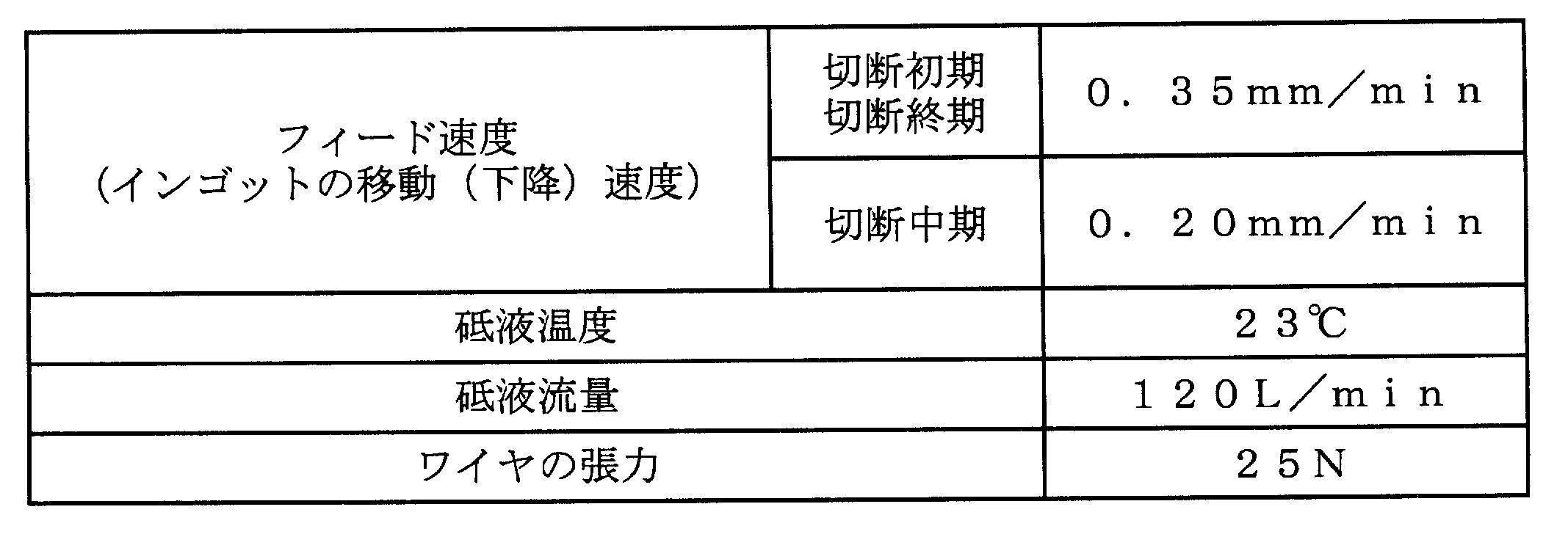
シリコンウェーハを製造する際、切断初期(例えば、波状ワイヤ7が図3Aの実線で示す位置を切断している場合)および切断終期(例えば、波状ワイヤ7が図3Aの二点鎖線で示す位置を切断している場合)におけるインゴットとワイヤとの接触部分は、切断中期(例えば、波状ワイヤ7が図3Aの一点鎖線で示す位置を切断している場合)の接触部分と比べて短くなる。このため、切断初期および切断終期にワイヤに作用する負荷は、切断中期に作用する負荷より小さくなる。
そこで、切断中にワイヤに作用する負荷の差を最小限に抑えるために、切断中期のフィード速度を、切断初期および切断終期のフィード速度よりも遅くしている。
図5に示すように、実験例1-1,1-2のシリコンウェーハについては、切断方向および走行方向の両方において、外縁部に対して略中央部がワイヤ進行方向と同じ方向(実験例1-1については図2における後ろ側、実験例1-2については前側)に凹む形状であることが確認できた。
このことから、実験例1-1,1-2のシリコンウェーハでは、切断方向および走行方向において、外縁部に対して略中央部が、ワイヤ進行方向と同じ方向に凹むドーム状に反っていると推定できる。すなわち、上記仮説が正しいことが確認できた。
一方、図6に示すように、比較例1-1,1-2のシリコンウェーハについては、切断方向および走行方向において、反り形状にワイヤ進行方向との相関が見られない。
通常、インゴットの切断により得られたシリコンウェーハに対し、エピタキシャル膜を形成する前に両面の研削が行われる。波状ワイヤ7を用いることで得られたシリコンウェーハの反りが、研削を行うことで消失してしまう可能性がある。
そこで、両面の研削により、シリコンウェーハの反りが消失しないことを確認する実験を行った。
本発明は、このような知見に基づいて完成されたものである。
また、本発明のシリコンウェーハの製造方法では、前記ワイヤとして、波状に癖付けされた波状ワイヤを用いることが好ましい。
なお、波状ワイヤとしては、長手方向の一端側から見たときに、円に見えるように螺旋状に癖付けしたものであっても良いし、長手方向の一端側から見たときに、直線に見えるように単に波状に癖付けしたものであっても良い。
そこで、本発明者は、鋭意研究を重ねた結果、フィード速度を適切に設定することで、切断方向の反りが滑らかな円弧状となるシリコンウェーハが得られる可能性があることに着目した。そこで、本発明者は、以下の実験3を行った。
まず、円柱状のインゴットのフィード速度をF、ワイヤとインゴットとの接触部分の長さをLとして、インゴットを切断する際のワイヤの仕事量Wを、以下の式(1)のように定義した。
W=F×L … (1)
実験1において説明したように、切断中期のフィード速度を、切断初期および切断終期のフィード速度よりも遅くしている。このため、図8に示すように、切断初期から切断中期に移行する前後、切断中期から切断終期に移行する前後には、仕事量Wの変化の割合が大きく異なっている。
一方、シリコンウェーハの切断方向の反りの形状に着目すると、仕事量Wの推移とほぼ一致することが確認できた。
以上のことから、仕事量Wが、インゴットの直径が最大となる切断位置で最大値となる略円弧状に変化するように、フィード速度を制御することで、切断方向の反りが略円弧状となるシリコンウェーハが得られると推定できる。すなわち、仕事量Wが滑らかな曲線状に変化するように、フィード速度を制御することで、切断方向の反りが滑らかな円弧状となるシリコンウェーハが得られると推定できる。
本発明の好ましい態様は、このような知見に基づいて完成されたものである。
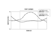
図9A,図9Bに示すように、切断方向および走行方向の両方について、エピタキシャル膜形成後のシリコンウェーハの反りは、インゴット(シリコンウェーハ)の直径が最大となる中心位置を中心にした、直径の50%(0.5×R(直径))の範囲(以下、切断中央範囲Aと称す)が特に大きくなることが確認できた。
このことから、エピタキシャル膜形成前に切断中央範囲Aの反りを大きくすることで、切断中央範囲Aにおけるエピタキシャル膜形成後の反りが小さくなると推定できる。そこで、この推定が正しいかを確認する実験4を行った。
まず、直線状ワイヤで製造したシリコンウェーハに対して研削を行い、強制的に切断中央範囲Aの反りを大きくした。そして、このシリコンウェーハについて、エピタキシャル膜を形成する前後の形状を調べた。その結果を図10A,図10Bに示す。図10A,図10Bに示すように、切断方向および走行方向の両方について、エピタキシャル膜形成後の切断中央範囲Aのシリコンウェーハの反りは、図9A,図9Bに示す場合と比べて小さくなることが確認できた。
なお、図9A,図9B,図10A,図10Bに結果を示すシリコンウェーハの直径は、300mmである。
このことから、切断中央範囲Aにおける仕事量Wを制御して、当該切断中央範囲Aにおける反りを大きくすることで、エピタキシャル膜形成後の反りを小さくできると推定できる。
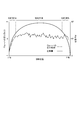
実験3の結果に基づく推定では、シリコンウェーハの切断方向の反りと仕事量Wとの推移がほぼ一致するため、フィード速度を略一定にした場合、シリコンウェーハの切断方向の反りの形状は、図11に示す仕事量Wの推移とほぼ一致すると推定できる。この場合、切断中央範囲Aの反りは、図9Aに反り形状を示すシリコンウェーハよりも大きくなると推定できる。
そして、仕事量Wが図11に示すように変化する場合、切断位置がインゴットの中心位置の場合の仕事量をWmax、切断中央範囲Aでの仕事量をWcntとすると、以下の式(2)の関係が満たされる。
Wcnt≧0.85×Wmax … (2)
本発明の好ましい態様は、このような知見に基づいて完成されたものである。
そこで、本発明者は、以下の実験5を行った。
張力を10N、15N、25N、30Nとしたこと以外は、上記実験1の実験例1-1と同様の条件で直径が300mmのインゴットを切断した。
その結果、張力が10N、30Nの場合に断線が発生し、15N、25Nの場合に断線が発生しないことが確認できた。
また、張力が15N、25Nの条件で製造したシリコンウェーハについて、WarpとBowとを算出した。Warpの算出結果を図12Aに、Bowの算出結果を図12Bにそれぞれ示す。
本発明の好ましい態様は、このような知見に基づいて完成されたものである。
以下、本発明の実施形態を図面を参照して説明する。
本実施形態においては、図2に示すようなワイヤソー1を用いて、インゴットTを切断する。ここで、インゴットTの形状は特に限定されないが、通常は円柱状である。また、インゴットTの直径は特に限定されないが、通常、100mm~450mmである。
そして、トラバーサ43,44を駆動するとともに、複数のメインローラ2とワイヤリール41,42とを回転させることで、波状ワイヤ7をメインローラ2の軸方向と略直交する方向に走行させ(ワイヤ走行工程)、2個の上側メインローラ21間に砥液Gを供給しつつ、インゴットTを下降させて走行中の波状ワイヤ7に押し当てることで、インゴットTを切断して複数のシリコンウェーハWFを製造する(切断工程)。
この際、インゴットTの直径が最大となる切断位置で、仕事量Wが最大値となるように、フィード速度を設定しても良い。また、このように、仕事量Wが略円弧状に変化するように切断位置によってフィード速度を変更しても良いし、切断位置によらずフィード速度を略一定にしても良い。
また、切断中央範囲Aの仕事量Wcntが上記式(2)の関係を満たすように、フィード速度を制御しても良い。
さらに、図11に示すように、切断中央範囲Aの下端側端部(中央から、下端側に直径(R)の25%移動した位置)Abでの仕事量をWb、上端側端部(中央から、上端側に直径(R)の25%移動した位置)Atでの仕事量をWtとした場合、仕事量Wbと仕事量Wtとは同じであっても良いし、異なっていてもよい。
上述したように、上記実施形態では、以下のような作用効果を奏することができる。
なお、本発明は上記実施形態にのみ限定されるものではなく、本発明の要旨を逸脱しない範囲内において種々の改良ならびに設計の変更などが可能である。
また、切断中央範囲Aの仕事量Wcntが上記式(2)の関係を満たさないように、フィード速度を制御しても良い。
さらに、波状に癖付けされていないワイヤを用いて、ドーム状に反るシリコンウェーハWFを製造してもよい。
7…波状ワイヤ(ワイヤ) T…インゴット
WF…シリコンウェーハ
Claims (7)
- ワイヤが螺旋状に巻き付けられた複数のメインローラを回転させることで、前記ワイヤを前記メインローラの軸方向と略直交する方向に走行させるワイヤ走行工程と、
前記ワイヤにインゴットを押し当てることで前記インゴットを切断し、外縁部に対して中央部が一方向に凹むドーム状に反った複数のシリコンウェーハを製造する切断工程とを行うことを特徴とするシリコンウェーハの製造方法。 - 請求項1に記載のシリコンウェーハの製造方法において、
前記ワイヤとして、波状に癖付けされた波状ワイヤを用いることを特徴とするシリコンウェーハの製造方法。 - 請求項2に記載のシリコンウェーハの製造方法において、
前記切断工程は、
円柱状の前記インゴットを前記波状ワイヤに押し当てるときの前記インゴットのフィード速度をF、
前記波状ワイヤと前記インゴットとの接触部分の長さをLとして、
円柱状の前記インゴットにおける当該インゴットの径方向の切断位置に対して、以下の式(1)で定義される仕事量Wが、前記インゴットの直径が最大となる切断位置で最大値となる略円弧状に変化するように、前記インゴットの前記フィード速度を制御することを特徴とするシリコンウェーハの製造方法。
W=F×L … (1) - 請求項3に記載のシリコンウェーハの製造方法において、
前記切断工程は、
前記インゴットの直径が最大となる切断位置での仕事量をWmax、
前記インゴットの直径が最大となる切断位置を中心とした前記インゴットの直径の50%の範囲での仕事量をWcntとして、
以下の式(2)で示す関係を満たすように前記インゴットの前記フィード速度を制御することを特徴とするシリコンウェーハの製造方法。
Wcnt≧0.85×Wmax … (2) - 請求項3または請求項4に記載のシリコンウェーハの製造方法において、
前記切断工程は、前記インゴットの切断開始から切断終了までの間、前記インゴットの前記フィード速度を略一定に維持するように制御することを特徴とするシリコンウェーハの製造方法。 - 請求項2から請求項5のいずれかに記載のシリコンウェーハの製造方法において、
前記切断工程は、張力が15N以上25N以下に設定された前記波状ワイヤに前記インゴットを押し当てることを特徴とするシリコンウェーハの製造方法。 - 請求項1から請求項6のいずれかに記載のシリコンウェーハの製造方法により製造されたことを特徴とするシリコンウェーハ。
Priority Applications (3)
| Application Number | Priority Date | Filing Date | Title |
|---|---|---|---|
| KR1020167025248A KR101880518B1 (ko) | 2014-02-20 | 2014-11-19 | 실리콘 웨이퍼의 제조 방법 |
| CN201480076001.2A CN106030764B (zh) | 2014-02-20 | 2014-11-19 | 硅晶片的制造方法和硅晶片 |
| DE112014006394.0T DE112014006394B4 (de) | 2014-02-20 | 2014-11-19 | Siliziumwaferherstellungsverfahren |
Applications Claiming Priority (2)
| Application Number | Priority Date | Filing Date | Title |
|---|---|---|---|
| JP2014-030719 | 2014-02-20 | ||
| JP2014030719A JP6281312B2 (ja) | 2014-02-20 | 2014-02-20 | シリコンウェーハの製造方法 |
Publications (1)
| Publication Number | Publication Date |
|---|---|
| WO2015125366A1 true WO2015125366A1 (ja) | 2015-08-27 |
Family
ID=53877895
Family Applications (1)
| Application Number | Title | Priority Date | Filing Date |
|---|---|---|---|
| PCT/JP2014/080632 Ceased WO2015125366A1 (ja) | 2014-02-20 | 2014-11-19 | シリコンウェーハの製造方法およびシリコンウェーハ |
Country Status (5)
| Country | Link |
|---|---|
| JP (1) | JP6281312B2 (ja) |
| KR (1) | KR101880518B1 (ja) |
| CN (1) | CN106030764B (ja) |
| DE (1) | DE112014006394B4 (ja) |
| WO (1) | WO2015125366A1 (ja) |
Cited By (5)
| Publication number | Priority date | Publication date | Assignee | Title |
|---|---|---|---|---|
| USD827819S1 (en) | 2017-04-07 | 2018-09-04 | St. Jude Medical, Cardiology Division, Inc. | Catheter handle |
| USD827818S1 (en) | 2017-04-07 | 2018-09-04 | St. Jude Medical, Cardiology Division, Inc. | Catheter handle |
| WO2018173693A1 (ja) * | 2017-03-21 | 2018-09-27 | 信越半導体株式会社 | インゴットの切断方法 |
| WO2022244421A1 (ja) * | 2021-05-20 | 2022-11-24 | 信越半導体株式会社 | シリコンウェーハの製造方法 |
| US11850369B2 (en) | 2016-04-08 | 2023-12-26 | St. Jude Medical, Cardiology Division, Inc. | Mapping variable loop catheter handle |
Families Citing this family (6)
| Publication number | Priority date | Publication date | Assignee | Title |
|---|---|---|---|---|
| DE102017202314A1 (de) * | 2017-02-14 | 2018-08-16 | Siltronic Ag | Drahtsäge, Drahtführungsrolle und Verfahren zum gleichzeitigen Abtrennen einer Vielzahl von Scheiben von einem Stab |
| JP7035777B2 (ja) * | 2017-06-02 | 2022-03-15 | 信越化学工業株式会社 | 半導体用基板およびその製造方法 |
| JP6717267B2 (ja) * | 2017-07-10 | 2020-07-01 | 株式会社Sumco | シリコンウェーハの製造方法 |
| JP7447828B2 (ja) * | 2021-01-12 | 2024-03-12 | 信越半導体株式会社 | ワークの切断方法 |
| JP7616020B2 (ja) * | 2021-11-04 | 2025-01-17 | 株式会社Sumco | 監視方法、監視プログラム、監視装置、ウェーハの製造方法、及びウェーハ |
| DE102024002895A1 (de) * | 2024-09-09 | 2026-03-12 | Siltronic Ag | Draht zum Auftrennen eines Werkstücks in Scheiben mittels Drahtsägens |
Citations (6)
| Publication number | Priority date | Publication date | Assignee | Title |
|---|---|---|---|---|
| JP2004276207A (ja) * | 2003-03-18 | 2004-10-07 | Kanai Hiroaki | マルチワイヤソー用ソーワイヤ |
| JP2008302618A (ja) * | 2007-06-08 | 2008-12-18 | Shin Etsu Handotai Co Ltd | 切断方法およびワイヤソー装置 |
| WO2009078130A1 (ja) * | 2007-12-19 | 2009-06-25 | Shin-Etsu Handotai Co., Ltd. | ワイヤソーによるワークの切断方法およびワイヤソー |
| JP2010023233A (ja) * | 2008-07-15 | 2010-02-04 | Sumitomo Metal Mining Co Ltd | 単結晶材料の面方位合わせ装置および面方位合わせ方法 |
| JP2013032278A (ja) * | 2008-09-08 | 2013-02-14 | Sumitomo Electric Ind Ltd | 基板の製造方法 |
| JP2014030876A (ja) * | 2012-08-02 | 2014-02-20 | Kanai Hiroaki | 固定砥粒式ソーワイヤ用のコアワイヤ |
Family Cites Families (7)
| Publication number | Priority date | Publication date | Assignee | Title |
|---|---|---|---|---|
| JP3274190B2 (ja) | 1992-09-26 | 2002-04-15 | 株式会社東芝 | 半導体エピタキシャル基板の製造方法 |
| JP3070430B2 (ja) * | 1995-02-17 | 2000-07-31 | 住友金属工業株式会社 | マルチワイヤソーによる切断方法及び装置 |
| JP2885270B2 (ja) * | 1995-06-01 | 1999-04-19 | 信越半導体株式会社 | ワイヤーソー装置及びワークの切断方法 |
| JP3299889B2 (ja) * | 1996-07-31 | 2002-07-08 | シャープ株式会社 | 太陽電池用ウエハの製造方法 |
| JP5250968B2 (ja) | 2006-11-30 | 2013-07-31 | 株式会社Sumco | エピタキシャルシリコンウェーハ及びその製造方法並びにエピタキシャル成長用シリコンウェーハ。 |
| JP2012121101A (ja) * | 2010-12-08 | 2012-06-28 | Japan Fine Steel Co Ltd | 固定砥粒ワイヤ |
| FR2988023A1 (fr) * | 2012-03-16 | 2013-09-20 | Sodetal Sas | Fil a scier, methode de fabrication d'un tel fil et utilisation |
-
2014
- 2014-02-20 JP JP2014030719A patent/JP6281312B2/ja active Active
- 2014-11-19 DE DE112014006394.0T patent/DE112014006394B4/de active Active
- 2014-11-19 WO PCT/JP2014/080632 patent/WO2015125366A1/ja not_active Ceased
- 2014-11-19 CN CN201480076001.2A patent/CN106030764B/zh active Active
- 2014-11-19 KR KR1020167025248A patent/KR101880518B1/ko active Active
Patent Citations (6)
| Publication number | Priority date | Publication date | Assignee | Title |
|---|---|---|---|---|
| JP2004276207A (ja) * | 2003-03-18 | 2004-10-07 | Kanai Hiroaki | マルチワイヤソー用ソーワイヤ |
| JP2008302618A (ja) * | 2007-06-08 | 2008-12-18 | Shin Etsu Handotai Co Ltd | 切断方法およびワイヤソー装置 |
| WO2009078130A1 (ja) * | 2007-12-19 | 2009-06-25 | Shin-Etsu Handotai Co., Ltd. | ワイヤソーによるワークの切断方法およびワイヤソー |
| JP2010023233A (ja) * | 2008-07-15 | 2010-02-04 | Sumitomo Metal Mining Co Ltd | 単結晶材料の面方位合わせ装置および面方位合わせ方法 |
| JP2013032278A (ja) * | 2008-09-08 | 2013-02-14 | Sumitomo Electric Ind Ltd | 基板の製造方法 |
| JP2014030876A (ja) * | 2012-08-02 | 2014-02-20 | Kanai Hiroaki | 固定砥粒式ソーワイヤ用のコアワイヤ |
Cited By (10)
| Publication number | Priority date | Publication date | Assignee | Title |
|---|---|---|---|---|
| US11850369B2 (en) | 2016-04-08 | 2023-12-26 | St. Jude Medical, Cardiology Division, Inc. | Mapping variable loop catheter handle |
| WO2018173693A1 (ja) * | 2017-03-21 | 2018-09-27 | 信越半導体株式会社 | インゴットの切断方法 |
| JP2018157158A (ja) * | 2017-03-21 | 2018-10-04 | 信越半導体株式会社 | インゴットの切断方法 |
| CN110447089A (zh) * | 2017-03-21 | 2019-11-12 | 信越半导体株式会社 | 铸块的切断方法 |
| TWI746817B (zh) * | 2017-03-21 | 2021-11-21 | 日商信越半導體股份有限公司 | 鑄塊的切斷方法 |
| CN110447089B (zh) * | 2017-03-21 | 2023-04-18 | 信越半导体株式会社 | 铸块的切断方法 |
| US11878385B2 (en) | 2017-03-21 | 2024-01-23 | Shin-Etsu Handotai Co., Ltd. | Method for slicing ingot |
| USD827819S1 (en) | 2017-04-07 | 2018-09-04 | St. Jude Medical, Cardiology Division, Inc. | Catheter handle |
| USD827818S1 (en) | 2017-04-07 | 2018-09-04 | St. Jude Medical, Cardiology Division, Inc. | Catheter handle |
| WO2022244421A1 (ja) * | 2021-05-20 | 2022-11-24 | 信越半導体株式会社 | シリコンウェーハの製造方法 |
Also Published As
| Publication number | Publication date |
|---|---|
| CN106030764A (zh) | 2016-10-12 |
| JP6281312B2 (ja) | 2018-02-21 |
| DE112014006394B4 (de) | 2024-06-06 |
| CN106030764B (zh) | 2018-10-30 |
| KR101880518B1 (ko) | 2018-07-20 |
| KR20160122795A (ko) | 2016-10-24 |
| DE112014006394T5 (de) | 2016-11-17 |
| JP2015156433A (ja) | 2015-08-27 |
Similar Documents
| Publication | Publication Date | Title |
|---|---|---|
| JP6281312B2 (ja) | シリコンウェーハの製造方法 | |
| CN101517710B (zh) | 切断方法以及外延晶片的制造方法 | |
| JP5256910B2 (ja) | グルーブローラの構造 | |
| US9707635B2 (en) | Method for slicing workpiece and wire saw | |
| JP7020286B2 (ja) | インゴットの切断方法及びワイヤーソー | |
| JP5135623B2 (ja) | 半導体インゴットの切断方法 | |
| JP2008078473A (ja) | 切断方法 | |
| KR102100839B1 (ko) | 워크의 절단방법 | |
| JP5639858B2 (ja) | インゴットの切断方法 | |
| CN113272101B (zh) | 工件的切断方法及工件的切断装置 | |
| JP5958430B2 (ja) | ワークの切断方法及びワイヤソー | |
| JP6753390B2 (ja) | ワイヤソー装置およびウェーハの製造方法 | |
| WO2016117294A1 (ja) | ワークの切断方法 | |
| JP7020454B2 (ja) | ワークの切断方法及びワイヤソー | |
| JP6493243B2 (ja) | ウェーハの製造方法 | |
| JP6277924B2 (ja) | インゴットの切断方法 | |
| CN108778623B (zh) | 线锯装置的制造方法及线锯装置 | |
| JP2007276048A (ja) | ワイヤによるワークの切断方法 | |
| JP4899088B2 (ja) | 半導体インゴットの切断方法 | |
| JP2007276047A (ja) | ワイヤによるワークの切断方法 |
Legal Events
| Date | Code | Title | Description |
|---|---|---|---|
| 121 | Ep: the epo has been informed by wipo that ep was designated in this application |
Ref document number: 14883032 Country of ref document: EP Kind code of ref document: A1 |
|
| WWE | Wipo information: entry into national phase |
Ref document number: 112014006394 Country of ref document: DE |
|
| ENP | Entry into the national phase |
Ref document number: 20167025248 Country of ref document: KR Kind code of ref document: A |
|
| 122 | Ep: pct application non-entry in european phase |
Ref document number: 14883032 Country of ref document: EP Kind code of ref document: A1 |