WO2015099079A1 - 封止フィルム、有機エレクトロルミネッセンス表示装置及び有機半導体デバイス - Google Patents
封止フィルム、有機エレクトロルミネッセンス表示装置及び有機半導体デバイス Download PDFInfo
- Publication number
- WO2015099079A1 WO2015099079A1 PCT/JP2014/084389 JP2014084389W WO2015099079A1 WO 2015099079 A1 WO2015099079 A1 WO 2015099079A1 JP 2014084389 W JP2014084389 W JP 2014084389W WO 2015099079 A1 WO2015099079 A1 WO 2015099079A1
- Authority
- WO
- WIPO (PCT)
- Prior art keywords
- film
- sealing
- layer
- sealing film
- block copolymer
- Prior art date
- Legal status (The legal status is an assumption and is not a legal conclusion. Google has not performed a legal analysis and makes no representation as to the accuracy of the status listed.)
- Ceased
Links
Images





Classifications
-
- B—PERFORMING OPERATIONS; TRANSPORTING
- B32—LAYERED PRODUCTS
- B32B—LAYERED PRODUCTS, i.e. PRODUCTS BUILT-UP OF STRATA OF FLAT OR NON-FLAT, e.g. CELLULAR OR HONEYCOMB, FORM
- B32B7/00—Layered products characterised by the relation between layers; Layered products characterised by the relative orientation of features between layers, or by the relative values of a measurable parameter between layers, i.e. products comprising layers having different physical, chemical or physicochemical properties; Layered products characterised by the interconnection of layers
- B32B7/04—Interconnection of layers
- B32B7/12—Interconnection of layers using interposed adhesives or interposed materials with bonding properties
-
- B—PERFORMING OPERATIONS; TRANSPORTING
- B32—LAYERED PRODUCTS
- B32B—LAYERED PRODUCTS, i.e. PRODUCTS BUILT-UP OF STRATA OF FLAT OR NON-FLAT, e.g. CELLULAR OR HONEYCOMB, FORM
- B32B7/00—Layered products characterised by the relation between layers; Layered products characterised by the relative orientation of features between layers, or by the relative values of a measurable parameter between layers, i.e. products comprising layers having different physical, chemical or physicochemical properties; Layered products characterised by the interconnection of layers
- B32B7/02—Physical, chemical or physicochemical properties
- B32B7/022—Mechanical properties
-
- B—PERFORMING OPERATIONS; TRANSPORTING
- B32—LAYERED PRODUCTS
- B32B—LAYERED PRODUCTS, i.e. PRODUCTS BUILT-UP OF STRATA OF FLAT OR NON-FLAT, e.g. CELLULAR OR HONEYCOMB, FORM
- B32B27/00—Layered products comprising a layer of synthetic resin
- B32B27/06—Layered products comprising a layer of synthetic resin as the main or only constituent of a layer, which is next to another layer of the same or of a different material
- B32B27/08—Layered products comprising a layer of synthetic resin as the main or only constituent of a layer, which is next to another layer of the same or of a different material of synthetic resin
-
- B—PERFORMING OPERATIONS; TRANSPORTING
- B32—LAYERED PRODUCTS
- B32B—LAYERED PRODUCTS, i.e. PRODUCTS BUILT-UP OF STRATA OF FLAT OR NON-FLAT, e.g. CELLULAR OR HONEYCOMB, FORM
- B32B27/00—Layered products comprising a layer of synthetic resin
- B32B27/28—Layered products comprising a layer of synthetic resin comprising synthetic resins not wholly covered by any one of the sub-groups B32B27/30 - B32B27/42
-
- B—PERFORMING OPERATIONS; TRANSPORTING
- B32—LAYERED PRODUCTS
- B32B—LAYERED PRODUCTS, i.e. PRODUCTS BUILT-UP OF STRATA OF FLAT OR NON-FLAT, e.g. CELLULAR OR HONEYCOMB, FORM
- B32B27/00—Layered products comprising a layer of synthetic resin
- B32B27/30—Layered products comprising a layer of synthetic resin comprising vinyl (co)polymers; comprising acrylic (co)polymers
- B32B27/302—Layered products comprising a layer of synthetic resin comprising vinyl (co)polymers; comprising acrylic (co)polymers comprising aromatic vinyl (co)polymers, e.g. styrenic (co)polymers
-
- B—PERFORMING OPERATIONS; TRANSPORTING
- B32—LAYERED PRODUCTS
- B32B—LAYERED PRODUCTS, i.e. PRODUCTS BUILT-UP OF STRATA OF FLAT OR NON-FLAT, e.g. CELLULAR OR HONEYCOMB, FORM
- B32B27/00—Layered products comprising a layer of synthetic resin
- B32B27/32—Layered products comprising a layer of synthetic resin comprising polyolefins
-
- B—PERFORMING OPERATIONS; TRANSPORTING
- B32—LAYERED PRODUCTS
- B32B—LAYERED PRODUCTS, i.e. PRODUCTS BUILT-UP OF STRATA OF FLAT OR NON-FLAT, e.g. CELLULAR OR HONEYCOMB, FORM
- B32B3/00—Layered products comprising a layer with external or internal discontinuities or unevennesses, or a layer of non-planar shape; Layered products comprising a layer having particular features of form
- B32B3/02—Layered products comprising a layer with external or internal discontinuities or unevennesses, or a layer of non-planar shape; Layered products comprising a layer having particular features of form characterised by features of form at particular places, e.g. in edge regions
- B32B3/08—Layered products comprising a layer with external or internal discontinuities or unevennesses, or a layer of non-planar shape; Layered products comprising a layer having particular features of form characterised by features of form at particular places, e.g. in edge regions characterised by added members at particular parts
-
- B—PERFORMING OPERATIONS; TRANSPORTING
- B32—LAYERED PRODUCTS
- B32B—LAYERED PRODUCTS, i.e. PRODUCTS BUILT-UP OF STRATA OF FLAT OR NON-FLAT, e.g. CELLULAR OR HONEYCOMB, FORM
- B32B7/00—Layered products characterised by the relation between layers; Layered products characterised by the relative orientation of features between layers, or by the relative values of a measurable parameter between layers, i.e. products comprising layers having different physical, chemical or physicochemical properties; Layered products characterised by the interconnection of layers
- B32B7/04—Interconnection of layers
-
- B—PERFORMING OPERATIONS; TRANSPORTING
- B32—LAYERED PRODUCTS
- B32B—LAYERED PRODUCTS, i.e. PRODUCTS BUILT-UP OF STRATA OF FLAT OR NON-FLAT, e.g. CELLULAR OR HONEYCOMB, FORM
- B32B7/00—Layered products characterised by the relation between layers; Layered products characterised by the relative orientation of features between layers, or by the relative values of a measurable parameter between layers, i.e. products comprising layers having different physical, chemical or physicochemical properties; Layered products characterised by the interconnection of layers
- B32B7/04—Interconnection of layers
- B32B7/10—Interconnection of layers at least one layer having inter-reactive properties
-
- G—PHYSICS
- G02—OPTICS
- G02B—OPTICAL ELEMENTS, SYSTEMS OR APPARATUS
- G02B5/00—Optical elements other than lenses
- G02B5/30—Polarising elements
- G02B5/3083—Birefringent or phase retarding elements
-
- H—ELECTRICITY
- H10—SEMICONDUCTOR DEVICES; ELECTRIC SOLID-STATE DEVICES NOT OTHERWISE PROVIDED FOR
- H10D—INORGANIC ELECTRIC SEMICONDUCTOR DEVICES
- H10D30/00—Field-effect transistors [FET]
- H10D30/60—Insulated-gate field-effect transistors [IGFET]
- H10D30/67—Thin-film transistors [TFT]
-
- H—ELECTRICITY
- H10—SEMICONDUCTOR DEVICES; ELECTRIC SOLID-STATE DEVICES NOT OTHERWISE PROVIDED FOR
- H10D—INORGANIC ELECTRIC SEMICONDUCTOR DEVICES
- H10D86/00—Integrated devices formed in or on insulating or conducting substrates, e.g. formed in silicon-on-insulator [SOI] substrates or on stainless steel or glass substrates
- H10D86/40—Integrated devices formed in or on insulating or conducting substrates, e.g. formed in silicon-on-insulator [SOI] substrates or on stainless steel or glass substrates characterised by multiple TFTs
- H10D86/451—Integrated devices formed in or on insulating or conducting substrates, e.g. formed in silicon-on-insulator [SOI] substrates or on stainless steel or glass substrates characterised by multiple TFTs characterised by the compositions or shapes of the interlayer dielectrics
-
- H—ELECTRICITY
- H10—SEMICONDUCTOR DEVICES; ELECTRIC SOLID-STATE DEVICES NOT OTHERWISE PROVIDED FOR
- H10D—INORGANIC ELECTRIC SEMICONDUCTOR DEVICES
- H10D86/00—Integrated devices formed in or on insulating or conducting substrates, e.g. formed in silicon-on-insulator [SOI] substrates or on stainless steel or glass substrates
- H10D86/40—Integrated devices formed in or on insulating or conducting substrates, e.g. formed in silicon-on-insulator [SOI] substrates or on stainless steel or glass substrates characterised by multiple TFTs
- H10D86/60—Integrated devices formed in or on insulating or conducting substrates, e.g. formed in silicon-on-insulator [SOI] substrates or on stainless steel or glass substrates characterised by multiple TFTs wherein the TFTs are in active matrices
-
- H—ELECTRICITY
- H10—SEMICONDUCTOR DEVICES; ELECTRIC SOLID-STATE DEVICES NOT OTHERWISE PROVIDED FOR
- H10K—ORGANIC ELECTRIC SOLID-STATE DEVICES
- H10K50/00—Organic light-emitting devices
- H10K50/80—Constructional details
- H10K50/84—Passivation; Containers; Encapsulations
- H10K50/841—Self-supporting sealing arrangements
-
- H—ELECTRICITY
- H10—SEMICONDUCTOR DEVICES; ELECTRIC SOLID-STATE DEVICES NOT OTHERWISE PROVIDED FOR
- H10K—ORGANIC ELECTRIC SOLID-STATE DEVICES
- H10K50/00—Organic light-emitting devices
- H10K50/80—Constructional details
- H10K50/86—Arrangements for improving contrast, e.g. preventing reflection of ambient light
-
- H—ELECTRICITY
- H10—SEMICONDUCTOR DEVICES; ELECTRIC SOLID-STATE DEVICES NOT OTHERWISE PROVIDED FOR
- H10K—ORGANIC ELECTRIC SOLID-STATE DEVICES
- H10K59/00—Integrated devices, or assemblies of multiple devices, comprising at least one organic light-emitting element covered by group H10K50/00
- H10K59/80—Constructional details
- H10K59/87—Passivation; Containers; Encapsulations
- H10K59/871—Self-supporting sealing arrangements
-
- H—ELECTRICITY
- H10—SEMICONDUCTOR DEVICES; ELECTRIC SOLID-STATE DEVICES NOT OTHERWISE PROVIDED FOR
- H10K—ORGANIC ELECTRIC SOLID-STATE DEVICES
- H10K59/00—Integrated devices, or assemblies of multiple devices, comprising at least one organic light-emitting element covered by group H10K50/00
- H10K59/80—Constructional details
- H10K59/8791—Arrangements for improving contrast, e.g. preventing reflection of ambient light
-
- B—PERFORMING OPERATIONS; TRANSPORTING
- B32—LAYERED PRODUCTS
- B32B—LAYERED PRODUCTS, i.e. PRODUCTS BUILT-UP OF STRATA OF FLAT OR NON-FLAT, e.g. CELLULAR OR HONEYCOMB, FORM
- B32B2250/00—Layers arrangement
- B32B2250/03—3 layers
-
- B—PERFORMING OPERATIONS; TRANSPORTING
- B32—LAYERED PRODUCTS
- B32B—LAYERED PRODUCTS, i.e. PRODUCTS BUILT-UP OF STRATA OF FLAT OR NON-FLAT, e.g. CELLULAR OR HONEYCOMB, FORM
- B32B2307/00—Properties of the layers or laminate
- B32B2307/40—Properties of the layers or laminate having particular optical properties
-
- B—PERFORMING OPERATIONS; TRANSPORTING
- B32—LAYERED PRODUCTS
- B32B—LAYERED PRODUCTS, i.e. PRODUCTS BUILT-UP OF STRATA OF FLAT OR NON-FLAT, e.g. CELLULAR OR HONEYCOMB, FORM
- B32B2307/00—Properties of the layers or laminate
- B32B2307/40—Properties of the layers or laminate having particular optical properties
- B32B2307/416—Reflective
-
- B—PERFORMING OPERATIONS; TRANSPORTING
- B32—LAYERED PRODUCTS
- B32B—LAYERED PRODUCTS, i.e. PRODUCTS BUILT-UP OF STRATA OF FLAT OR NON-FLAT, e.g. CELLULAR OR HONEYCOMB, FORM
- B32B2307/00—Properties of the layers or laminate
- B32B2307/40—Properties of the layers or laminate having particular optical properties
- B32B2307/418—Refractive
-
- B—PERFORMING OPERATIONS; TRANSPORTING
- B32—LAYERED PRODUCTS
- B32B—LAYERED PRODUCTS, i.e. PRODUCTS BUILT-UP OF STRATA OF FLAT OR NON-FLAT, e.g. CELLULAR OR HONEYCOMB, FORM
- B32B2307/00—Properties of the layers or laminate
- B32B2307/40—Properties of the layers or laminate having particular optical properties
- B32B2307/42—Polarizing, birefringent, filtering
-
- B—PERFORMING OPERATIONS; TRANSPORTING
- B32—LAYERED PRODUCTS
- B32B—LAYERED PRODUCTS, i.e. PRODUCTS BUILT-UP OF STRATA OF FLAT OR NON-FLAT, e.g. CELLULAR OR HONEYCOMB, FORM
- B32B2307/00—Properties of the layers or laminate
- B32B2307/50—Properties of the layers or laminate having particular mechanical properties
- B32B2307/51—Elastic
-
- B—PERFORMING OPERATIONS; TRANSPORTING
- B32—LAYERED PRODUCTS
- B32B—LAYERED PRODUCTS, i.e. PRODUCTS BUILT-UP OF STRATA OF FLAT OR NON-FLAT, e.g. CELLULAR OR HONEYCOMB, FORM
- B32B2307/00—Properties of the layers or laminate
- B32B2307/50—Properties of the layers or laminate having particular mechanical properties
- B32B2307/54—Yield strength; Tensile strength
-
- B—PERFORMING OPERATIONS; TRANSPORTING
- B32—LAYERED PRODUCTS
- B32B—LAYERED PRODUCTS, i.e. PRODUCTS BUILT-UP OF STRATA OF FLAT OR NON-FLAT, e.g. CELLULAR OR HONEYCOMB, FORM
- B32B2405/00—Adhesive articles, e.g. adhesive tapes
-
- B—PERFORMING OPERATIONS; TRANSPORTING
- B32—LAYERED PRODUCTS
- B32B—LAYERED PRODUCTS, i.e. PRODUCTS BUILT-UP OF STRATA OF FLAT OR NON-FLAT, e.g. CELLULAR OR HONEYCOMB, FORM
- B32B2457/00—Electrical equipment
- B32B2457/20—Displays, e.g. liquid crystal displays, plasma displays
-
- B—PERFORMING OPERATIONS; TRANSPORTING
- B32—LAYERED PRODUCTS
- B32B—LAYERED PRODUCTS, i.e. PRODUCTS BUILT-UP OF STRATA OF FLAT OR NON-FLAT, e.g. CELLULAR OR HONEYCOMB, FORM
- B32B2457/00—Electrical equipment
- B32B2457/20—Displays, e.g. liquid crystal displays, plasma displays
- B32B2457/206—Organic displays, e.g. OLED
-
- B—PERFORMING OPERATIONS; TRANSPORTING
- B32—LAYERED PRODUCTS
- B32B—LAYERED PRODUCTS, i.e. PRODUCTS BUILT-UP OF STRATA OF FLAT OR NON-FLAT, e.g. CELLULAR OR HONEYCOMB, FORM
- B32B2581/00—Seals; Sealing equipment; Gaskets
Definitions
- the present invention relates to a sealing film, and an organic electroluminescence display device and an organic semiconductor device provided with the sealing film.
- Organic electroluminescent elements hereinafter sometimes referred to as “organic EL elements” as appropriate
- organic electronic devices including elements such as organic semiconductor elements may be provided with a sealing member.
- a sealing member By providing such a sealing member in such a manner as to seal the organic material inside the device, it is possible to prevent the organic material from being deteriorated by water vapor and oxygen, thereby preventing a decrease in the performance of the device. be able to.
- a sealing film including an inorganic layer has been proposed (see Patent Document 1).
- an antireflection film may be provided in order to prevent external light from being reflected on the screen.
- an antireflection film one having a circularly polarizing plate in which a linearly polarizing plate and a quarter-wave plate are combined is known (see Patent Document 2).
- the present inventor attempted to provide an adhesive layer on the sealing film.
- an adhesive layer on the sealing film.
- the present invention was devised in view of the above-mentioned problems, and when combined with an antireflection film provided with a circularly polarizing plate, it is difficult to cause a decrease in antireflection performance, has excellent handling properties, and enables good sealing.
- An object is to provide a sealing film, and an organic electroluminescence display device and an organic semiconductor device including the sealing film.
- the inventor has intensively studied to solve the above problems.
- the inventor is a sealing film including a base film, a sealing layer, and an adhesive layer in this order, and the tensile elastic modulus of the sealing film falls within a predetermined range, and the base of the sealing film
- the present inventor is less likely to cause a decrease in antireflection performance when combined with an antireflection film provided with a circularly polarizing plate, has excellent handling properties, and can be sealed well.
- the present invention was completed with the knowledge that there was. That is, the present invention is as follows.
- a sealing film comprising a base film, a sealing layer and an adhesive layer in this order,
- the sealing film has a tensile modulus of 1000 MPa or more;
- the sealing film whose retardation of the layer part provided in the said sealing layer side rather than the said base film of the said sealing film after sealing is 20 nm or less.
- the adhesive layer contains a hydrogenated block copolymer elastomer.
- the hydrogenated block copolymer elastomer is a hydride obtained by hydrogenating 90% or more of the total unsaturated bonds of the block copolymer,
- the block copolymer comprises an aromatic vinyl compound unit as a main component, two or more polymer blocks [A] per copolymer molecule, and a chain conjugated diene compound unit as a main component. Having one or more polymer blocks [B] per molecule
- the ratio (wA / wB) of the weight fraction wA of all polymer blocks [A] to the weight fraction wB of all polymer blocks [B] in the entire block copolymer (wA / wB) is 20/80 to 60/40.
- the sealing film according to [2].
- the antireflection performance when combined with an antireflection film provided with a circularly polarizing plate, the antireflection performance is unlikely to deteriorate, the handling property is excellent, and the sealing film can be satisfactorily sealed.
- An organic electroluminescence display device and an organic semiconductor device including a film can be provided.
- FIG. 1 is a cross-sectional view schematically showing an example of the sealing film of the present invention.
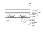
- FIG. 2 is a longitudinal sectional view schematically showing the organic EL display device according to the first embodiment of the present invention.
- FIG. 3 is a perspective view schematically showing an assembly included in the organic EL display device according to the first embodiment of the present invention.
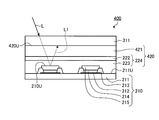
- FIG. 4 is a longitudinal sectional view schematically showing an organic EL display device according to the second embodiment of the present invention.
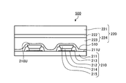
- FIG. 5 is a longitudinal sectional view schematically showing an organic EL display device according to the third embodiment of the present invention.
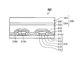
- FIG. 6 is a longitudinal sectional view schematically showing an organic EL display device according to the fourth embodiment of the present invention.
- FIG. 1 is a cross-sectional view schematically showing an example of the sealing film of the present invention.
- FIG. 2 is a longitudinal sectional view schematically showing the organic EL display device according to the first embodiment of the present invention.
- FIG. 3 is a perspective view schematically showing an
- FIG. 7 is a longitudinal sectional view schematically showing an organic EL display device according to the fifth embodiment of the present invention.
- FIG. 8 is a longitudinal sectional view schematically showing an organic semiconductor device according to the sixth embodiment of the present invention.
- FIG. 9 is a vertical cross-sectional view schematically showing structures manufactured in the examples and comparative examples of the present invention.
- the term “long” means that the film has a length of 5 times or more, preferably 10 times or more, and specifically a roll. It has a length enough to be wound up into a shape and stored or transported. Although the upper limit of the magnification of the length with respect to the width is not particularly limited, it can be usually 5000 times or less.
- polarizing plate and “1 ⁇ 4 wavelength plate” include not only a rigid member but also a flexible member such as a resin film.
- nx represents a refractive index in a direction (in-plane direction) perpendicular to the thickness direction of the film and giving the maximum refractive index.
- ny represents the refractive index in the in-plane direction of the film and perpendicular to the nx direction.
- d represents the thickness of the film.
- This retardation can be measured using a commercially available phase difference measuring apparatus (for example, “WPA-micro” manufactured by Photonic Lattice) or the Senarmon method.
- the measurement wavelength of in-plane retardation is 550 nm unless otherwise specified.
- FIG. 1 is a cross-sectional view schematically showing an example of the sealing film of the present invention.
- the sealing film 100 includes a base film 110, a sealing layer 120, and an adhesive layer 130 in this order.
- the sealing film 100 is usually used for sealing the element in an organic electronic device including elements such as an organic EL element and an organic semiconductor element. If this sealing film 100 is used, since the element with which a device is equipped can be sealed favorably, the deterioration by the water and oxygen of the organic material contained in an element can be prevented effectively.
- a resin film is usually used.
- a transparent resin from the viewpoint of making the sealing film useful for a portion that is required to transmit light in a display device and a light source device.
- a certain resin is transparent means that the base film formed of the resin has a light transmittance that is high enough to be used for optical applications.
- a resin having a total light transmittance of 70% or more, preferably 80% or more, more preferably 90% or more is desirable when the total light transmittance is measured using a test piece having a thickness of 1 mm as a resin. .
- thermoplastic resin for example, any of a thermoplastic resin, a thermosetting resin, an ultraviolet curable resin, and an electron beam curable resin can be used.
- thermoplastic resin is preferable because it is easy to process.
- thermoplastic resins include polyester resins, polyacrylate resins, olefin resins, and the like.
- an alicyclic olefin resin is a resin containing an alicyclic olefin polymer and other optional components as required.
- the alicyclic olefin resin has low hygroscopicity and excellent mechanical strength.
- the alicyclic olefin resin has a small amount of outgas emission in processes such as vapor deposition and sputtering when forming the sealing layer. Therefore, a sealing film with high barrier performance can be obtained by using a film made of an alicyclic olefin resin as the base film.
- a base film produced by melt extrusion of an alicyclic olefin resin has good surface smoothness and small surface protrusions that can cause cracks in the sealing layer. It is not necessary to increase the thickness of the sealing layer in order to obtain a stop layer, and the productivity and flexibility are excellent.
- the alicyclic olefin polymer is an amorphous thermoplastic polymer having an alicyclic structure in the main chain and / or side chain.
- the alicyclic olefin polymer usually has a structure obtained by polymerization of an alicyclic olefin.
- the alicyclic structure in the alicyclic olefin polymer may be a saturated alicyclic hydrocarbon (cycloalkane) structure or an unsaturated alicyclic hydrocarbon (cycloalkene) structure. From the viewpoint of mechanical strength and heat resistance, a cycloalkane structure is preferred.
- the number of carbon atoms constituting one alicyclic structure is usually 4 or more, preferably 5 or more, and usually 30 or less, preferably 20 or less, more preferably 15 or less.
- the number of carbon atoms constituting one alicyclic structure is in the above range, mechanical strength, heat resistance, and film formability are highly balanced, which is preferable.
- the proportion of structural units having an alicyclic structure in the entire alicyclic olefin polymer is preferably 55% by weight or more, more preferably 70% by weight or more, and particularly preferably 90% by weight or more. It is preferable from a transparency and heat resistant viewpoint that the ratio of the structural unit which has an alicyclic structure in an alicyclic olefin polymer exists in this range.
- alicyclic olefin polymer examples include a norbornene polymer, a monocyclic olefin polymer, a cyclic conjugated diene polymer, a vinyl alicyclic hydrocarbon polymer, and a hydride thereof.
- norbornene polymers can be suitably used because of their good transparency and moldability.
- norbornene polymers examples include a ring-opening polymer of a monomer having a norbornene structure, a ring-opening copolymer of a monomer having a norbornene structure and an arbitrary monomer, or a hydride thereof; norbornene An addition polymer of a monomer having a structure, an addition copolymer of a monomer having a norbornene structure and an arbitrary monomer, or a hydride thereof.
- a ring-opening (co) polymer hydride of a monomer having a norbornene structure is particularly suitable from the viewpoints of moldability, heat resistance, low hygroscopicity, dimensional stability, lightness, and the like.
- (co) polymer refers to a polymer and a copolymer.
- Examples of the monomer having a norbornene structure include bicyclo [2.2.1] hept-2-ene (common name: norbornene), tricyclo [4.3.0.1 2,5 ] deca-3,7. -Diene (common name: dicyclopentadiene), 7,8-benzotricyclo [4.3.0.1 2,5 ] dec-3-ene (common name: methanotetrahydrofluorene), tetracyclo [4.4. 0.1 2,5 . 1 7,10 ] dodec-3-ene (common name: tetracyclododecene), and derivatives of these compounds (for example, those having a substituent in the ring).
- examples of the substituent include an alkyl group, an alkylene group, and a polar group. Moreover, these substituents may be the same or different, and a plurality thereof may be bonded to the ring. Moreover, the monomer which has a norbornene structure may be used individually by 1 type, and may be used combining two or more types by arbitrary ratios.
- Examples of the polar group include heteroatoms or atomic groups having heteroatoms.
- Examples of the hetero atom include an oxygen atom, a nitrogen atom, a sulfur atom, a silicon atom, and a halogen atom.
- Specific examples of the polar group include a carboxyl group, a carbonyloxycarbonyl group, an epoxy group, a hydroxyl group, an oxy group, an ester group, a silanol group, a silyl group, an amino group, a nitrile group, and a sulfonic acid group.
- optional monomers capable of ring-opening copolymerization with a monomer having a norbornene structure include, for example, monocyclic olefins such as cyclohexene, cycloheptene, and cyclooctene and derivatives thereof; and cyclic conjugates such as cyclohexadiene and cycloheptadiene. Dienes and derivatives thereof; and the like.
- the optional monomer capable of ring-opening copolymerization with a monomer having a norbornene structure one type may be used alone, or two or more types may be used in combination at any ratio.
- a ring-opening polymer of a monomer having a norbornene structure, and a ring-opening copolymer of any monomer copolymerizable with a monomer having a norbornene structure are, for example, a known ring-opening monomer. It can be produced by polymerization or copolymerization in the presence of a polymerization catalyst.
- ⁇ -olefin is preferable, and ethylene is more preferable.
- the arbitrary monomer which can carry out addition copolymerization with the monomer which has a norbornene structure may be used individually by 1 type, and may be used combining two or more types by arbitrary ratios.
- An addition copolymer of a monomer having a norbornene structure and an addition copolymer of any monomer that can be copolymerized with a monomer having a norbornene structure include, for example, a monomer of a known addition polymerization catalyst. It can be produced by polymerization or copolymerization in the presence.
- An addition polymer and a hydride of a polymer such as an addition copolymer of a monomer having a norbornene structure and an arbitrary monomer copolymerizable therewith can be produced by any production method.
- the hydride of the polymer described above preferably has a carbon-carbon unsaturated bond of 90% or more in the presence of a known hydrogenation catalyst containing a transition metal such as nickel or palladium in a solution of these polymers. It can be produced by hydrogenation.
- the molecular weight of the alicyclic olefin polymer contained in the alicyclic olefin resin is appropriately selected according to the purpose of use.
- the weight average molecular weight (Mw) of the alicyclic olefin polymer is usually 10,000 or more, preferably 15,000 or more, more preferably 20,000 or more, and usually 100,000 or less, preferably 80,000 or less. More preferably, it is 50,000 or less.
- Mw weight average molecular weight
- the weight average molecular weight of the alicyclic olefin polymer can be measured as a value in terms of polyisoprene by gel permeation chromatography using cyclohexane as a solvent.
- toluene may be used as a solvent.
- the weight average molecular weight can be measured as a value in terms of polystyrene.
- the proportion of the alicyclic olefin polymer in the alicyclic olefin resin is preferably 67% by weight to 100% by weight, more preferably 77% by weight to 100% by weight.
- the above alicyclic olefin polymers may be used alone or in combination of two or more at any ratio.
- alicyclic olefin resin examples include, for example, antioxidants, heat stabilizers, light stabilizers, ultraviolet absorbers, antistatic agents, dispersants, chlorine scavengers, flame retardants, and crystallization nuclei.
- Agent, reinforcing agent, antiblocking agent, antifogging agent, mold release agent, pigment, organic or inorganic filler, neutralizing agent, lubricant, decomposition agent, metal deactivator, antifouling agent, antibacterial agent optional Examples thereof include additives such as polymers and thermoplastic elastomers. Moreover, these may be used individually by 1 type and may be used combining two or more types by arbitrary ratios.
- the amount of these additives may be within a range that does not impair the effects of the present invention.
- the amount of the additive is usually 0 to 50 parts by weight, preferably 0 to 30 parts by weight with respect to 100 parts by weight of the alicyclic olefin polymer contained in the alicyclic olefin resin.
- the resin forming the base film preferably has a high glass transition temperature.
- the specific glass transition temperature of the resin forming the base film is preferably 110 ° C. or higher, more preferably 130 ° C. or higher, and particularly preferably 160 ° C. or higher. Since a resin having a high glass transition temperature hardly causes thermal shrinkage due to a temperature change, it is possible to suppress a decrease in the barrier property of the sealing film in a high temperature environment.
- limiting in particular in the upper limit of the glass transition temperature of resin which forms a base film Preferably it is 300 degrees C or less.
- the base film may be a single-layer film composed of one layer, or a multilayer film including two or more layers.
- the thickness of the base film is preferably 10 ⁇ m or more, more preferably 30 ⁇ m or more, preferably 500 ⁇ m or less, more preferably 250 ⁇ m or less.
- a base film having such a thickness is excellent in both mechanical strength and barrier properties in a well-balanced manner.
- the retardation of the base film can be arbitrarily set according to the use of the sealing film.
- the retardation of the base film is preferably small.
- the retardation of the base film is preferably 10 nm or less, and more preferably 5 nm or less.
- a base film has a quarter wavelength retardation.
- the retardation of 1 ⁇ 4 wavelength is usually within the range of ⁇ 65 nm, preferably ⁇ 30 nm, more preferably ⁇ 10 nm from the 1 ⁇ 4 value of 550 nm which is the measurement wavelength, or the center value.
- the retardation is usually in the range of ⁇ 65 nm, preferably ⁇ 30 nm, more preferably ⁇ 10 nm.
- the manufacturing method of the base film is arbitrary.
- a base film when manufacturing a base film from a thermoplastic resin, a base film can be manufactured by shape
- the melt molding method can be classified into, for example, an extrusion molding method, a press molding method, an inflation molding method, an injection molding method, a blow molding method, and a stretch molding method.
- an extrusion molding method, an inflation molding method, or a press molding method is preferable in order to obtain a base film excellent in mechanical strength, surface accuracy, and the like.
- the extrusion molding method is particularly preferable in order to produce a base film efficiently and easily.
- a stretching step of stretching the film may be performed when the base film is produced.
- a stretched film can be obtained as a base film.
- the stretching method include a uniaxial stretching method such as a method of uniaxial stretching in the longitudinal direction using a difference in peripheral speed of the roll, a uniaxial stretching method in the transverse direction using a tenter stretching machine; a simultaneous biaxial stretching method, Examples thereof include a biaxial stretching method such as a sequential biaxial stretching method; and a method of stretching obliquely using a tenter stretching machine.
- the diagonal direction represents a direction not parallel to both the vertical direction and the horizontal direction.
- the sealing layer is a layer having a function capable of blocking water.
- this sealing layer usually has a function of blocking not only water but also oxygen. Since the sealing film can block water and oxygen by this sealing layer, the organic material in the device provided with the sealing film can be prevented from being deteriorated by water vapor and oxygen.
- the degree of the function of the sealing agent that can block water is represented by the water vapor transmission rate as follows.
- the water vapor transmission rate of the sealing layer is usually 1.0 g / m 2 ⁇ day or less, preferably 0.2 g / m 2 ⁇ day or less, more preferably 0.1 g / m 2 ⁇ day or less.
- the sealing layer is formed of an inorganic material.
- inorganic materials tend to cause scratches and cracks.
- the sealing film of the present invention since the sealing layer is sandwiched between the base film and the adhesive layer, scratches and cracks due to external force are unlikely to occur. Therefore, even when the sealing layer is formed of an inorganic material, the sealing layer is unlikely to be scratched or cracked, and the barrier property is not easily impaired.
- the alicyclic olefin resin that can be used as a material for the base film often has low affinity with other materials, but if the sealing layer is formed of an inorganic material, the alicyclic olefin resin can be used. It can have a high affinity with the substrate film.
- the inorganic material can usually have a high affinity with a hydrogenated block copolymer elastomer that can form an adhesive layer. Therefore, when a sealing layer made of an inorganic material is provided between the base film and the adhesive layer, the adhesion between the base film and the adhesive layer can be improved.
- Preferred examples of the inorganic material that can form the sealing layer include metals (including metalloids); metal compounds such as metal oxides, metal nitrides, and metal oxynitrides; DLC (diamond-like carbon). It is done.
- the metal include aluminum and silicon.
- materials containing at least silicon, such as silicon oxide, nitride, and nitride oxide, are particularly preferable.
- DLC is particularly preferable from the viewpoint of affinity with an alicyclic olefin resin that can be a material of the base film.
- Examples of the silicon oxide include SiO x .
- x is usually larger than 1.4, preferably larger than 1.5, and usually smaller than 2.0, preferably from 1.9 from the viewpoint of achieving both transparency and barrier properties of the sealing layer. It is a small number.
- SiOC can also be mentioned as an oxide of silicon.
- Examples of silicon nitride include SiN y .
- y is a number usually larger than 0.5, preferably larger than 1.2, and usually smaller than 1.5 from the viewpoint of achieving both transparency and barrier properties of the sealing layer.
- Examples of silicon nitride oxide include SiO p N q .
- the sealing layer when importance is attached to improving the adhesion of the sealing layer, it is preferable that the sealing layer is an oxygen-rich film with 1 ⁇ p ⁇ 2.0 and 0 ⁇ q ⁇ 1.0. In the case where importance is placed on improving the barrier property of the sealing layer, it is preferable that the sealing layer be a nitrogen-rich film with 0 ⁇ p ⁇ 0.8 and 0.8 ⁇ q ⁇ 1.3.
- oxide, nitride, and nitride oxide of aluminum examples include AlO x , AiN y , and AlO p N q .
- SiO p N q and AlO x can be used as more preferable materials.
- these inorganic materials may be used individually by 1 type, and may be used combining two or more types by arbitrary ratios.
- the thickness of the sealing layer is preferably 3 nm or more, more preferably 10 nm or more, particularly preferably 100 nm or more, preferably 2500 nm or less, more preferably 2000 nm or less, and particularly preferably 1000 nm or less.
- the formation method of the sealing layer is arbitrary.
- a deposition method such as a vapor deposition method, a sputtering method, an ion plating method, an ion beam assisted vapor deposition method, an arc discharge plasma vapor deposition method, a thermal CVD method, or a plasma CVD method can be used.
- a vapor deposition method such as a vapor deposition method, a sputtering method, an ion plating method, an ion beam assisted vapor deposition method, an arc discharge plasma vapor deposition method, a thermal CVD method, or a plasma CVD method
- evaporated particles having an appropriate energy are generated, and a high-density film can be formed.
- a flexible sealing layer can be formed by adjusting a gas component used for forming a film. Can be effectively suppressed. Furthermore, when forming the sealing layer containing several types of components, you may vapor-deposit or sputter those components simultaneously.
- the adhesive layer is a layer that can have adhesiveness to the member when the sealing film is bonded to another member.
- the adhesive layer preferably has sufficiently high adhesiveness with the inorganic substance.
- the peel strength required to peel the adhesive layer from the glass plate is usually 5 N / cm or more, preferably 10 N / cm or more.
- the peel strength required to peel the adhesive layer from the glass plate is usually 5 N / cm or more, preferably 10 N / cm or more.
- it is 200 N / cm or less.
- the adhesive layer is preferably a flexible layer. Since the adhesive layer is flexible, when an external force is applied to the device provided with the sealing film, the adhesive layer can be deformed to absorb the external force, so that damage to the elements in the device due to the external force can be prevented. Can be prevented. In addition, when the element is sealed with the sealing film, the adhesive layer can be deformed in accordance with the shape of the surface of the element. The release of the stop film can be stably prevented.
- the flexibility of the adhesive layer is expressed by a tensile elastic modulus
- the adhesive layer usually has a tensile elastic modulus smaller than that of the base film, preferably 1500 MPa or less, more preferably 1000 MPa or less, particularly preferably 800 MPa or less.
- the tensile modulus is a value measured at 23 ° C.
- the minimum of the said tensile elasticity modulus Usually, it is 0.1 Mpa or more.
- the material for the adhesive layer having adhesiveness and flexibility as described above it is usually preferable to use a resin, and it is preferable to use an elastomer resin.
- the elastomer resin is a resin containing an elastomer and optional components as necessary.
- An elastomer is a polymer having rubber elasticity at room temperature without vulcanization. Here, room temperature usually means 25 ° C.
- Elastomer resins generally do not contain residual solvent, or even if they contain it, the amount thereof is small, so there is little outgas. Therefore, since the elastomer resin hardly generates gas under a low pressure environment, the adhesive layer itself can be prevented from becoming a gas generation source.
- a block copolymer elastomer and a hydrogenated block copolymer elastomer are preferable.
- the block copolymer elastomer is an elastomer made of a block copolymer.
- the hydrogenated block copolymer elastomer is an elastomer made of a hydride of a block copolymer.
- the properties of the block copolymer and its hydride can be adjusted by the type and ratio of the polymer block contained in the molecular structure.
- the block copolymer and its hydride are elastomers
- the block copolymer is usually a polymer block as a rubber component (that is, a soft segment) having elasticity in the molecule, and for preventing plastic deformation.
- a polymer block as a molecular constraining component that is, a hard segment.
- the block copolymer is preferably an aromatic vinyl compound-conjugated diene block copolymer.
- the aromatic vinyl compound-conjugated diene block copolymer is a polymer block [A] having an aromatic vinyl compound unit as a main component and a polymer block having a chain conjugated diene compound unit as a main component [A].
- the aromatic vinyl compound unit refers to a structural unit having a structure formed by polymerizing an aromatic vinyl compound.
- the chain conjugated diene compound unit refers to a structural unit having a structure formed by polymerizing a chain conjugated diene compound.
- the elastomer used as the material for the adhesive layer is mainly composed of two or more polymer blocks [A] and a chain conjugated diene compound unit per molecule of the copolymer, the main component of which is an aromatic vinyl compound unit.
- a hydride obtained by hydrogenating a specific block copolymer having one or more polymer blocks [B] per molecule of the copolymer is preferable.
- the hydride obtained by hydrogenating this specific block copolymer will be described.
- the polymer block [A] included in the specific block copolymer has an aromatic vinyl compound unit.
- the aromatic vinyl compound corresponding to the aromatic vinyl compound unit included in the polymer block [A] include styrene, ⁇ -methylstyrene, 2-methylstyrene, 3-methylstyrene, 4-methylstyrene, 2, 4-diisopropylstyrene, 2,4-dimethylstyrene, 4-t-butylstyrene, 5-t-butyl-2-methylstyrene, 4-monochlorostyrene, dichlorostyrene, 4-monofluorostyrene, 4-phenylstyrene, etc.
- the content of the aromatic vinyl compound unit in the polymer block [A] is usually 90% by weight or more, preferably 95% by weight or more, more preferably 99% by weight or more.
- the polymer block [A] may contain an arbitrary structural unit in addition to the aromatic vinyl compound unit.
- the arbitrary structural unit include a chain conjugated diene compound unit and a structural unit having a structure formed by polymerizing a vinyl compound other than an aromatic vinyl compound.
- Examples of the chain conjugated diene compound corresponding to the chain conjugated diene compound unit include, for example, the same examples as those exemplified as the chain conjugated diene compound corresponding to the chain conjugated diene compound unit included in the polymer block [B]. Is mentioned.
- strand-shaped conjugated diene compound may be used individually by 1 type, and may be used combining two or more types by arbitrary ratios.
- vinyl compounds other than aromatic vinyl compounds include: chain vinyl compounds; cyclic vinyl compounds; vinyl compounds having a nitrile group, alkoxycarbonyl group, hydroxycarbonyl group, or halogen group; unsaturated cyclic acid anhydrides; Examples thereof include saturated imide compounds.
- chain olefins such as 4,6-dimethyl-1-heptene
- cyclic olefins such as vinylcyclohexane
- the content of an arbitrary structural unit in the polymer block [A] is usually 10% by weight or less, preferably 5% by weight or less, more preferably 1% by weight or less.
- the number of polymer blocks [A] in one molecule of the block copolymer is usually 2 or more, usually 5 or less, preferably 4 or less, more preferably 3 or less.
- the plurality of polymer blocks [A] in one molecule may be the same as or different from each other.
- the weight average molecular weight of the polymer block having the maximum weight average molecular weight in the polymer block [A] is expressed as Mw (A1).
- the weight average molecular weight of the polymer block having the smallest weight average molecular weight is Mw (A2).
- the ratio “Mw (A1) / Mw (A2)” between Mw (A1) and Mw (A2) is preferably 2.0 or less, more preferably 1.5 or less, and particularly preferably 1.2 or less. It is. Thereby, the dispersion
- the polymer block [B] of the block copolymer has a chain conjugated diene compound unit.
- Examples of the chain conjugated diene compound corresponding to the chain conjugated diene compound unit included in the polymer block [B] include 1,3-butadiene, isoprene, 2,3-dimethyl-1,3-butadiene, 1, Examples include 3-pentadiene.
- One of these may be used alone, or two or more of these may be used in combination at any ratio. Among them, those not containing a polar group are preferable in terms of hygroscopicity, and 1,3-butadiene and isoprene are particularly preferable.
- the content of the chain conjugated diene compound unit in the polymer block [B] is usually 90% by weight or more, preferably 95% by weight or more, more preferably 99% by weight or more.
- the polymer block [B] may contain an arbitrary structural unit in addition to the chain conjugated diene compound unit.
- the arbitrary structural unit include an aromatic vinyl compound unit and a structural unit having a structure formed by polymerizing a vinyl compound other than the aromatic vinyl compound.
- the structural unit having a structure formed by polymerizing these aromatic vinyl compound units and vinyl compounds other than the aromatic vinyl compound for example, it may be contained in the polymer block [A]. What was illustrated is mentioned.
- the content of an arbitrary structural unit in the polymer block [B] is usually 10% by weight or less, preferably 5% by weight or less, more preferably 1% by weight or less.
- the content of an arbitrary structural unit in the polymer block [B] is usually 10% by weight or less, preferably 5% by weight or less, more preferably 1% by weight or less.
- the number of polymer blocks [B] in one molecule of the block copolymer is usually 1 or more, but may be 2 or more. When the number of polymer blocks [B] in the block copolymer is 2 or more, the polymer blocks [B] may be the same as or different from each other.
- the weight average molecular weight of the polymer block having the largest weight average molecular weight in the polymer block [B] is expressed as Mw ( B1)
- the weight average molecular weight of the polymer block having the smallest weight average molecular weight is Mw (B2).
- the ratio “Mw (B1) / Mw (B2)” between Mw (B1) and Mw (B2) is preferably 2.0 or less, more preferably 1.5 or less, and particularly preferably 1.2 or less. It is. Thereby, the dispersion
- the block copolymer block may be a chain block or a radial block.
- a chain type block is preferable because of its excellent mechanical strength.
- both ends thereof are polymer blocks [A] because the stickiness of the elastomer resin can be suppressed to a desired low value.
- a particularly preferred block form of the block copolymer is a triblock copolymer in which the polymer block [A] is bonded to both ends of the polymer block [B]; the polymer block [B] on both ends of the polymer block [A]. ], And a polymer block [A] is bonded to the other end of each of the polymer blocks [B].
- a triblock copolymer of [A]-[B]-[A] is particularly preferable because it can be easily produced and physical properties such as viscosity can be in a desired range.
- the ratio of the weight fraction wA in which the entire polymer block [A] occupies the entire block copolymer and the weight fraction wB in which the entire polymer block [B] occupies the entire block copolymer is usually 20/80 or more, preferably 30/70 or more, and usually 60/40 or less, preferably 55/45 or less.
- the ratio wA / wB is usually 20/80 or more, preferably 30/70 or more, and usually 60/40 or less, preferably 55/45 or less.
- the weight average molecular weight (Mw) of the block copolymer is usually 30,000 or more, preferably 40,000 or more, more preferably 50,000 or more, and usually 200,000 or less, preferably 150,000 or less. More preferably, it is 100,000 or less.
- the weight average molecular weight of the block copolymer can be measured as a value in terms of polystyrene by gel permeation chromatography (GPC) using tetrahydrofuran (THF) as a solvent.
- GPC gel permeation chromatography
- THF tetrahydrofuran
- the molecular weight distribution (Mw / Mn) of the block copolymer is preferably 3 or less, more preferably 2 or less, particularly preferably 1.5 or less, and preferably 1.0 or more.
- Mn represents a number average molecular weight.
- Examples of the method for producing a block copolymer include, for example, the following production methods 1 and 2 when producing a block copolymer having three polymer blocks.
- the material called “monomer composition” includes not only a mixture of two or more substances but also a material composed of a single substance.
- the monomer composition (a1) and the monomer composition (a2) may be the same or different.
- (Manufacturing method 2) The 1st process of polymerizing the monomer composition (a1) containing an aromatic vinyl compound, and forming polymer block [A], At one end of the polymer block [A], the monomer composition (b1) containing a chain conjugated diene compound is polymerized to form the polymer block [B], and the diblock of [A]-[B] A second step of forming a polymer; And a third step of obtaining a block copolymer by coupling the ends of the diblock polymer on the polymer block [B] side with a coupling agent.
- radical polymerization, anion polymerization, cation polymerization, coordination anion polymerization, coordination cation polymerization and the like can be used.
- radical polymerization, anion polymerization, cation polymerization and the like are performed by living polymerization
- a method in which living polymerization is performed by living anion polymerization is particularly preferable.
- the polymerization of the monomer composition is usually 0 ° C. or higher, preferably 10 ° C. or higher, more preferably 20 ° C. or higher, and usually 100 ° C. or lower, preferably 80 ° C. or lower, more preferably in the presence of a polymerization initiator. Can be performed in a temperature range of 70 ° C. or lower.
- examples of the polymerization initiator include monoorganolithium such as n-butyllithium, sec-butyllithium, t-butyllithium, hexyllithium; dilithiomethane, 1,4-dilithiobutane, 1,4- And polyfunctional organolithium compounds such as dilithio-2-ethylcyclohexane; One of these may be used alone, or two or more of these may be used in combination at any ratio.
- monoorganolithium such as n-butyllithium, sec-butyllithium, t-butyllithium, hexyllithium
- dilithiomethane 1,4-dilithiobutane
- 1,4- And polyfunctional organolithium compounds such as dilithio-2-ethylcyclohexane
- solution polymerization and slurry polymerization can be used as the form of the polymerization reaction.
- reaction heat can be easily removed.
- an inert solvent in which the polymer obtained in each step can be dissolved can be used as the solvent.
- the inert solvent include aliphatic hydrocarbons such as n-pentane, isopentane, n-hexane, n-heptane, and isooctane; alicyclic carbonization such as cyclopentane, cyclohexane, methylcyclopentane, methylcyclohexane, and decalin.
- Aromade such as benzene and toluene; and the like. One of these may be used alone, or two or more of these may be used in combination at any ratio.
- alicyclic hydrocarbons are preferably used as the solvent because they can be used as they are as an inert solvent for the hydrogenation reaction and the solubility of the block copolymer is good.
- the amount of the solvent used is usually 200 to 2000 parts by weight with respect to 100 parts by weight of all the monomers used.
- a randomizer can be used in order to prevent only one component chain from becoming long.
- a Lewis base compound it is preferable to use, for example, a Lewis base compound as a randomizer.
- Lewis base compounds include ether compounds such as dimethyl ether, diethyl ether, diisopropyl ether, dibutyl ether, tetrahydrofuran, diphenyl ether, ethylene glycol diethyl ether, and ethylene glycol methyl phenyl ether; and tetramethylethylenediamine, trimethylamine, triethylamine, pyridine, Tertiary amine compounds; alkali metal alkoxide compounds such as potassium-t-amyl oxide and potassium-t-butyl oxide; phosphine compounds such as triphenylphosphine; and the like. One of these may be used alone, or two or more of these may be used in combination at any ratio.
- Hydride of specific block copolymer As the elastomer that is the material of the adhesive layer of the sealing film according to the present invention, it is preferable to use a hydride of the specific block copolymer described above. By using a specific block copolymer after hydrogenation, the amount of outgas generated from the adhesive layer can be further reduced.
- This hydride of the block copolymer is obtained by hydrogenating the unsaturated bond of the specific block copolymer described above.
- the unsaturated bond of the block copolymer includes both aromatic and non-aromatic carbon-carbon unsaturated bonds in the main chain and side chain of the block copolymer.
- the hydrogenation rate is usually 90% or more, preferably 97% or more, more preferably 99% or more of the total unsaturated bonds of the block copolymer. The higher the hydrogenation rate, the better the heat resistance and light resistance of the adhesive layer.
- the hydrogenation rate of the hydride can be determined by measurement by 1 H-NMR.
- the hydrogenation rate of the non-aromatic unsaturated bond is preferably 95% or more, more preferably 99% or more.
- the hydrogenation rate of the aromatic carbon-carbon unsaturated bond is preferably 90% or more, more preferably 93% or more, and particularly preferably 95% or more.
- the glass transition temperature of the polymer block obtained by hydrogenating the polymer block [A] is increased, so that the heat resistance of the adhesive layer is effective. Can be enhanced.
- the photoelastic coefficient of the adhesive layer can be lowered to make it difficult for the retardation during adhesion to be exhibited.
- the weight average molecular weight (Mw) of the hydride of the block copolymer is usually 30,000 or more, preferably 40,000 or more, more preferably 45,000 or more, and usually 200,000 or less, preferably 150,000. Below, more preferably 100,000 or less.
- the weight average molecular weight of the hydride of the block copolymer can be measured in terms of polystyrene by gel permeation chromatography using tetrahydrofuran as a solvent.
- the molecular weight distribution (Mw / Mn) of the hydride of the block copolymer is preferably 3 or less, more preferably 2 or less, particularly preferably 1.5 or less, and preferably 1.0 or more.
- the weight fraction wA of the whole polymer block [A] in the whole block copolymer, and the weight fraction wB in which the whole polymer block [B] occupies the whole block copolymer is usually the same value as the ratio wA / wB in the block copolymer before hydrogenation.
- the hydride of the block copolymer preferably has an alkoxysilyl group in its molecular structure.
- the block copolymer hydride having an alkoxysilyl group can be obtained, for example, by bonding an alkoxysilyl group to a hydride of a block copolymer having no alkoxysilyl group.
- an alkoxysilyl group may be directly bonded to the hydride of the block copolymer, and may be bonded via a divalent organic group such as an alkylene group.
- the hydride of a block copolymer having an alkoxysilyl group is particularly excellent in adhesion to materials such as glass, inorganic substances, and metals. Therefore, when sealing the element of an organic electronics device with the sealing film of this invention, the adhesiveness of an adhesive layer and an element can be made especially high. Therefore, the adhesive layer can maintain a sufficient adhesive force even after being exposed to a high-temperature and high-humidity environment, which is usually performed in the reliability evaluation of organic electronics devices, for a long time.
- the amount of the alkoxysilyl group introduced is usually 0.1 parts by weight or more, preferably 0.2 parts by weight or more, more preferably 0.1 parts by weight or more with respect to 100 parts by weight of the hydride of the block copolymer before introduction of the alkoxysilyl group. It is 3 parts by weight or more, usually 10 parts by weight or less, preferably 5 parts by weight or less, more preferably 3 parts by weight or less. If the introduction amount of the alkoxysilyl group falls within the above range, the degree of crosslinking between the alkoxysilyl groups decomposed with moisture or the like can be prevented from becoming excessively high, so that the adhesiveness with the adhesive layer can be kept high. it can.
- the amount of alkoxysilyl group introduced can be measured by 1 H-NMR spectrum. In addition, when the introduction amount of the alkoxysilyl group is measured, if the introduction amount is small, the number of integrations can be increased.
- the molecular weight of the hydride of the block copolymer having an alkoxysilyl group is usually larger than the molecular weight of the hydride of the block copolymer before introducing the alkoxysilyl group because the amount of the alkoxysilyl group to be introduced is small. It does not change. However, when the alkoxysilyl group is introduced, the hydride of the block copolymer is modified in the presence of peroxide, so that the hydride crosslinks and cleaves and the molecular weight distribution changes greatly. Tend.
- the weight average molecular weight of the hydride of the block copolymer having an alkoxysilyl group is usually 30,000 or more, preferably 40,000 or more, more preferably 50,000 or more, and usually 200,000 or less, preferably 150. Or less, more preferably 120,000 or less.
- the weight average molecular weight of the hydride of the block copolymer having an alkoxysilyl group can be measured as a value in terms of polystyrene by gel permeation chromatography using tetrahydrofuran as a solvent.
- the molecular weight distribution (Mw / Mn) of the hydride of the block copolymer having an alkoxysilyl group is usually 3.5 or less, preferably 2.5 or less, particularly preferably 2.0 or less, preferably 1 0.0 or more.
- Mw and Mn of the hydride of the block copolymer having an alkoxysilyl group are within this range, good mechanical strength and tensile elongation of the adhesive layer can be maintained.
- the method for producing a hydride of a block copolymer as described above usually includes hydrogenating the specific block copolymer described above.
- a hydrogenation method that can increase the hydrogenation rate and has less chain-breaking reaction of the block copolymer is preferable.
- Examples of such a preferable hydrogenation method include hydrogenation using a hydrogenation catalyst containing at least one metal selected from the group consisting of nickel, cobalt, iron, titanium, rhodium, palladium, platinum, ruthenium, and rhenium.
- a hydrogenation catalyst may be used individually by 1 type, and may be used combining two or more types by arbitrary ratios.
- the hydrogenation catalyst either a heterogeneous catalyst or a homogeneous catalyst can be used.
- the hydrogenation reaction is preferably performed in an organic solvent.
- the heterogeneous catalyst may be used as it is, for example, as a metal or a metal compound, or may be used by being supported on a suitable carrier.
- suitable carrier include activated carbon, silica, alumina, calcium carbonate, titania, magnesia, zirconia, diatomaceous earth, silicon carbide, calcium fluoride, and the like.
- the supported amount of the catalyst is usually 0.1% by weight or more, preferably 1% by weight or more, and usually 60% by weight or less, preferably 50% by weight or less based on the total amount of the catalyst and the carrier.
- the specific surface area of the supported catalyst is preferably 100 m 2 / g to 500 m 2 / g.
- the average pore diameter of the supported catalyst is preferably 100 mm or more, more preferably 200 mm or more, preferably 1000 mm or less, preferably 500 mm or less.
- the specific surface area can be obtained by measuring the nitrogen adsorption amount and using the BET equation.
- the average pore diameter can be measured by a mercury intrusion method.
- the homogeneous catalyst for example, a catalyst obtained by combining a nickel, cobalt, titanium or iron compound and an organometallic compound; an organometallic complex catalyst such as rhodium, palladium, platinum, ruthenium or rhenium;
- an organometallic complex catalyst such as rhodium, palladium, platinum, ruthenium or rhenium;
- the nickel, cobalt, titanium, or iron compound include acetylacetonato compounds, carboxylates, and cyclopentadienyl compounds of each metal.
- organometallic compound examples include organoaluminum compounds such as alkylaluminum such as triethylaluminum and triisobutylaluminum, aluminum halide such as diethylaluminum chloride and ethylaluminum dichloride, and alkylaluminum hydride such as diisobutylaluminum hydride; And organic lithium compounds.
- organoaluminum compounds such as alkylaluminum such as triethylaluminum and triisobutylaluminum, aluminum halide such as diethylaluminum chloride and ethylaluminum dichloride, and alkylaluminum hydride such as diisobutylaluminum hydride; And organic lithium compounds.
- organometallic complex catalysts include transition metal complexes such as dihydrido-tetrakis (triphenylphosphine) ruthenium, dihydrido-tetrakis (triphenylphosphine) iron, bis (cyclooctadiene) nickel, and bis (cyclopentadienyl) nickel. Is mentioned.
- the amount of the hydrogenation catalyst used is usually 0.01 parts by weight or more, preferably 0.05 parts by weight or more, more preferably 0.1 parts by weight or more, and usually 100 parts by weight with respect to 100 parts by weight of the block copolymer. It is not more than parts by weight, preferably not more than 50 parts by weight, more preferably not more than 30 parts by weight.
- the temperature of the hydrogenation reaction is usually 10 ° C. or higher, preferably 50 ° C. or higher, more preferably 80 ° C. or higher, and usually 250 ° C. or lower, preferably 200 ° C. or lower, more preferably 180 ° C. or lower.
- the hydrogen pressure during the hydrogenation reaction is usually 0.1 MPa or more, preferably 1 MPa or more, more preferably 2 MPa or more, and usually 30 MPa or less, preferably 20 MPa or less, more preferably 10 MPa or less.
- a hydride of the block copolymer is obtained as a product.
- the product after this hydrogenation reaction may be used as it is. Further, the product after the hydrogenation reaction may be further subjected to any treatment as necessary. For example, you may perform the process which introduce
- a method for introducing an alkoxysilyl group into a hydride of a block copolymer for example, a hydride of a block copolymer before introducing an alkoxysilyl group, an ethylenically unsaturated silane compound, a peroxide
- a method of reacting in the presence can be used.
- ethylenically unsaturated silane compound those capable of graft polymerization with a hydride of a block copolymer and capable of introducing an alkoxysilyl group into the hydride of the block copolymer can be used.
- Examples of such ethylenically unsaturated silane compounds include vinyltrimethoxysilane, vinyltriethoxysilane, allyltrimethoxysilane, allyltriethoxysilane, dimethoxymethylvinylsilane, diethoxymethylvinylsilane, p-styryltrimethoxysilane, p-styryltriethoxysilane, 3-methacryloxypropyltrimethoxysilane, 3-methacryloxypropylmethyldimethoxysilane, 3-methacryloxypropyltriethoxysilane, 3-methacryloxypropylmethyldiethoxysilane, 3-acryloxypropyltri Examples include methoxysilane, 3-acryloxypropyltriethoxysilane, and 2-norbornen-5-yltrimethoxysilane.
- vinyltrimethoxysilane, vinyltriethoxysilane, allyltrimethoxysilane, allyltriethoxysilane, dimethoxymethylvinylsilane, diethoxymethylvinylsilane, and p-styryltrimethoxysilane are preferable.
- an ethylenically unsaturated silane compound may be used individually by 1 type, and may be used combining two or more types by arbitrary ratios.
- the amount of the ethylenically unsaturated silane compound is usually 0.1 parts by weight or more, preferably 0.2 parts by weight or more, based on 100 parts by weight of the hydride of the block copolymer before introducing the alkoxysilyl group.
- the amount is preferably 0.3 parts by weight or more, usually 10 parts by weight or less, preferably 5 parts by weight or less, more preferably 3 parts by weight or less.
- peroxides examples include dibenzoyl peroxide, t-butyl peroxyacetate, 2,2-di- (t-butylperoxy) butane, t-butylperoxybenzoate, t-butylcumyl peroxide, Milperoxide, di-t-hexyl peroxide, 2,5-dimethyl-2,5-di (t-butylperoxyhexane), di-t-butyl peroxide, 2,5-dimethyl-2,5- Organic peroxides such as di (t-butylperoxy) hexane-3, t-butylhydroperoxide, t-butylperoxyisobutyrate, lauroyl peroxide, dipropionyl peroxide, p-menthane hydroperoxide Can be mentioned.
- t-butyl cumyl peroxide dicumyl peroxide, di-t-hexyl peroxide, 2,5-dimethyl-2,5- Di (t-butylperoxyhexane), di-t-butyl peroxide and the like are preferable.
- a peroxide may be used individually by 1 type and may be used in combination of 2 or more type.
- the amount of the peroxide is usually 0.01 parts by weight or more, preferably 0.2 parts by weight or more, more preferably 0 parts by weight based on 100 parts by weight of the hydride of the block copolymer before introducing the alkoxysilyl group. .3 parts by weight or more, usually 5 parts by weight or less, preferably 3 parts by weight or less, more preferably 2 parts by weight or less.
- the method of reacting the hydride of the block copolymer with the ethylenically unsaturated silane compound in the presence of a peroxide can be performed using, for example, a superheated kneader and a reactor.
- a block copolymer hydride, an ethylenically unsaturated silane compound and a peroxide mixture are heated and melted at a temperature equal to or higher than the melting temperature of the block copolymer hydride in a biaxial kneader. Then, by kneading for a desired time, an alkoxysilyl group can be introduced into the hydride of the block copolymer.
- the specific temperature is usually 180 ° C.
- the heat kneading time is usually 0.1 minutes or longer, preferably 0.2 minutes or longer, more preferably 0.3 minutes or longer, and usually 15 minutes or shorter, preferably 10 minutes or shorter, more preferably 5 minutes or shorter. It is. When continuous kneading equipment such as a twin-screw kneader or a short-screw extruder is used, kneading and extrusion can be performed continuously with the residence time being in the above range.
- the hydride of the block copolymer obtained by the above-described method is usually obtained as a reaction liquid containing a hydride of the block copolymer, a hydrogenation catalyst, and a polymerization catalyst. Therefore, the hydride of the block copolymer can be recovered from the reaction solution after removing the hydrogenation catalyst and the polymerization catalyst from the reaction solution by a method such as filtration and centrifugation.
- a method of recovering the hydride of the block copolymer from the reaction solution for example, a steam coagulation method in which the solvent is removed from the solution in which the hydride of the block copolymer is dissolved by steam stripping; the solvent is removed under reduced pressure heating. Direct desolvation method; a coagulation method in which a solution is poured into a poor solvent of the block copolymer hydride to precipitate and solidify the hydride of the block copolymer; and the like.
- the form of the recovered hydride of the block copolymer is preferably in the form of a pellet so that it can be easily subjected to subsequent molding or modification reaction.
- the molten hydride is extruded from a die into a strand shape, cooled, cut into pellets by a pelletizer, You may use for shaping
- the obtained solidified product may be dried and then extruded in a molten state by an extruder and may be formed into pellets in the same manner as described above and used for various moldings.
- Optional ingredients examples of optional components that can be contained in the elastomer resin that can be used as the material of the adhesive layer include, for example, a plasticizer for adjusting the glass transition temperature and elastic modulus, a light stabilizer for improving weather resistance and heat resistance, and an ultraviolet ray. Absorbers, antioxidants, lubricants, inorganic fillers and the like can be mentioned. Moreover, arbitrary components may be used individually by 1 type, and may be used combining two or more types by arbitrary ratios.
- Plasticizers for adjusting the glass transition temperature and flexibility include, for example, polyisobutene, hydrogenated polyisobutene, hydrogenated polyisoprene, hydrogenated 1,3-pentadiene petroleum resin, hydrogenated cyclopentadiene petroleum resin, hydrogenation Examples include styrene / indene petroleum resins.
- the blending amount of these plasticizers is usually 40 parts by weight or less with respect to 100 parts by weight of the elastomer resin, and is appropriately selected according to the purpose of adjusting the resin characteristics.
- a hindered amine light stabilizer is preferable, and the structure includes, for example, 3,5-di-tert-butyl-4-hydroxyphenyl group, 2,2,6,6-tetramethylpiperidyl group, or 1 , 2,2,6,6-pentamethyl-4-piperidyl group and the like are particularly preferable.
- the light stabilizer examples include 1,2,3,4-butanetetracarboxylic acid, 1,2,2,6,6-pentamethyl-4-piperidinol and 3,9-bis (2-hydroxy-1, 1-dimethylethyl) -2,4,8,10-tetraoxaspiro [5,5] undecane esterified product, 1,6-hexanediamine-N, N′-bis (2,2,6,6) -Tetramethyl-4-piperidyl) and polycondensate of morpholine-2,4,6-trichloro-1,3,5-triazine, 1- [2- [3- (3,5-di-t- Butyl-4-hydroxyphenyl) propionyloxy] ethyl] -4- [3-3,5-di-t-butyl-4-hydroxyphenyl) propionyloxy] -2,2,6,6-tetramethylpiperidine, 2 -(3,5-di-tert-butyl-4- Hydroxybenzyl
- N, N′-bis (2,2,6,6-tetramethyl-4-N-methylpiperidyl) -N, N′-diformyl-alkylenediamines N, N′-bis (2,2,6,6-tetramethyl-4-N-methylpiperidyl), N, N, N′-bis (2,2,6,6-tetramethyl-4-piperidyl) -N, N′-diformylalkylenediamine, N, N′-bis (2,2,6,6-tetramethyl- 4-piperidyl) -N, N′-bisalkylene fatty acid amides, poly [ ⁇ 6- (1,1,3,3-tetramethylbutyl) amino-1,3,5-triazine-2,4-diyl ⁇ ⁇ (2,2,6,6-tetramethyl-4-piperidyl) imino ⁇ hexamethylene ⁇ (2,2,6,6-tetramethyl-4-piperidyl) imino ⁇ ] is preferred,
- the amount of the light stabilizer is usually 0.01 parts by weight or more, preferably 0.02 parts by weight or more, more preferably 0.03 parts by weight or more, with respect to 100 parts by weight of the hydride of the block copolymer. Usually 5 parts by weight or less, preferably 2 parts by weight or less, more preferably 1 part by weight or less.
- Examples of the ultraviolet absorber include benzophenone ultraviolet absorbers, salicylic acid ultraviolet absorbers, and benzotriazole ultraviolet absorbers.
- Examples of benzophenone-based ultraviolet absorbers include 2,4-dihydroxybenzophenone, 2-hydroxy-4-methoxybenzophenone, 2-hydroxy-4-methoxybenzophenone-5-sulfonic acid trihydrate, 2-hydroxy-4- Octyloxybenzophenone, 4-dodecaloxy-2-hydroxybenzophenone, 4-benzyloxy-2-hydroxybenzophenone, 2,2 ', 4,4'-tetrahydroxybenzophenone, 2,2'-dihydroxy-4,4'-dimethoxy Examples include benzophenone.
- salicylic acid ultraviolet absorbers examples include phenyl salicylate, 4-t-butylphenyl-2-hydroxybenzoate, phenyl-2-hydroxybenzoate, 2,4-di-t-butylphenyl-3,5. -Di-t-butyl-4-hydroxybenzoate, hexadecyl-3,5-di-t-butyl-4-hydroxybenzoate and the like.
- benzotriazole ultraviolet absorber examples include 2- (2-hydroxy-5-methylphenyl) 2H-benzotriazole and 2- (3-t-butyl-2-hydroxy-5-methylphenyl) -5.
- the amount of the ultraviolet absorber is usually 0.01 parts by weight or more, preferably 0.02 parts by weight or more, more preferably 0.04 parts by weight or more with respect to 100 parts by weight of the hydride of the block copolymer. Usually, it is 1 part by weight or less, preferably 0.5 part by weight or less, more preferably 0.3 part by weight or less.
- the light resistance of the adhesive layer can be improved by using the ultraviolet absorber above the lower limit of the above range, further improvement is difficult to obtain even if it is used in excess of the upper limit.
- antioxidants examples include phosphorus antioxidants, phenol antioxidants, sulfur antioxidants, and the like, and phosphorus antioxidants with less coloring are preferable.
- phosphorus antioxidants include triphenyl phosphite, diphenylisodecyl phosphite, phenyl diisodecyl phosphite, tris (nonylphenyl) phosphite, tris (dinonylphenyl) phosphite, and tris (2,4-diphenyl).
- phenolic antioxidants include pentaerythrityl tetrakis [3- (3,5-di-t-butyl-4-hydroxyphenyl) propionate], 2,2-thio-diethylenebis [3- (3,5-di-t-butyl-4-hydroxyphenyl) propionate], octadecyl-3- (3,5-di-t-butyl-4-hydroxyphenyl) propionate, 3,9-bis ⁇ 2- [ 3- (3-tert-butyl-4-hydroxy-5-methylphenyl) propionyloxy] -1,1-dimethylethyl ⁇ -2,4,8,10-tetraoxaspiro [5,5] undecane, Mention may be made of compounds such as 3,5-trimethyl-2,4,6-tris (3,5-di-tert-butyl-4-hydroxybenzyl) benzene.
- sulfur-based antioxidant examples include dilauryl-3,3′-thiodipropionate, dimyristyl-3,3′-thiodipropionate, distearyl-3,3′-thiodipropionate, laurylstearyl- 3,3′-thiodipropionate, pentaerythritol-tetrakis- ( ⁇ -lauryl-thio-propionate), 3,9-bis (2-dodecylthioethyl) -2,4,8,10-tetraoxaspiro [ 5,5] can include compounds such as undecane.
- the amount of the antioxidant is usually 0.01 parts by weight or more, preferably 0.05 parts by weight or more, more preferably 0.1 parts by weight or more with respect to 100 parts by weight of the hydride of the block copolymer. Usually, it is 1 part by weight or less, preferably 0.5 part by weight or less, more preferably 0.3 part by weight or less.
- the method of mixing the block copolymer hydride and the optional component is, for example, by dissolving the optional component in a suitable solvent and mixing it with the block copolymer hydride solution, and then removing the solvent.
- a method of recovering an elastomer resin containing an arbitrary component a method of kneading a hydride of a block copolymer in a molten state and kneading with an arbitrary component in a kneader such as a twin-screw kneader, a roll, a Brabender, or an extruder And so on.
- the resin forming the adhesive layer has high transparency.
- the total light transmittance measured by using the resin forming the adhesive layer as a test piece having a thickness of 1 mm is usually 70% or more, preferably 80% or more, more preferably 90% or more.
- the glass transition temperature of the resin forming the adhesive layer is usually 30 ° C. or higher, preferably 50 ° C. or higher, more preferably 70 ° C. or higher, and usually 200 ° C. or lower, preferably 180 ° C. or lower, more preferably 160 ° C. or lower. It is.
- the resin may have a plurality of glass transition temperatures. In that case, the highest glass transition temperature of the resin is preferably within the above range.
- the organic component contained in the device is not thermally deteriorated, and is closer to the sealing layer than the base film of the sealing film after sealing. It becomes easy to keep the retardation of the provided layer portion within a desired range.
- the thickness of the adhesive layer is preferably 10 ⁇ m or more, more preferably 15 ⁇ m or more, further preferably 20 ⁇ m or more, particularly preferably 40 ⁇ m or more, preferably 500 ⁇ m or less, more preferably 200 ⁇ m or less, still more preferably 150 ⁇ m or less, particularly preferably Preferably it is 100 micrometers or less.
- the thickness of the adhesive layer equal to or more than the lower limit of the above range, the adhesive layer can be produced by an extrusion molding method.
- it has this thickness, it has a sufficient sealing function, and even if a small foreign substance is mixed in the adhesive layer, it prevents the adhesive layer from becoming uneven in thickness due to the foreign substance. it can.
- the bending after bonding can be suppressed and a uniform sealing film can be formed, and the thickness of the sealing film can be reduced.
- the adhesive layer is usually prepared as a long film, and a sealing film is produced using this film.
- the adhesive layer can be produced, for example, by forming the above-mentioned adhesive layer material into a film shape.
- a melt molding method, a solution casting method, or the like can be used as the molding method. More specifically, the melt molding method can be classified into an extrusion molding method, a press molding method, an inflation molding method, an injection molding method, a blow molding method, a stretch molding method, and the like.
- the extrusion molding method, the inflation molding method and the press molding method are preferable.
- the extrusion molding method is preferable from the viewpoint of efficiently and easily producing a film. Particularly preferred.
- the sealing film may include an arbitrary layer as necessary in addition to the base film, the sealing layer, and the adhesive layer. For example, you may provide an antiblocking layer in the surface on the opposite side to the sealing layer of a base film. By providing an antiblocking layer, blocking of the sealing film can be prevented. Moreover, the surface of a sealing film can also be protected at the time of a preservation
- the anti-blocking layer is, for example, a method of coating a release agent such as a silicone release agent, a long-chain alkyl release agent, a fluorine release agent, or molybdenum sulfide; a method of forming a resin layer containing a lubricant such as inert particles; Or the like.
- the sealing film may include an antistatic layer, a hard coat layer, a conductivity imparting layer, a contamination preventing layer, an uneven structure layer, and the like.
- the sealing film has a tensile elastic modulus of usually 1000 MPa or more, preferably 1200 MPa or more, more preferably 1400 MPa or more at a measurement temperature of 23 ° C.
- the upper limit of the tensile modulus of the sealing film is usually 4000 MPa or less, preferably 3500 MPa or less, more preferably 3000 MPa or less.
- the method of adjusting the tensile elasticity modulus of a sealing film in the said range For example, the method of adjusting the material and thickness of a base film and an adhesive layer appropriately is mentioned.
- the material of the adhesive layer tends to have a low tensile modulus. Therefore, the tensile elastic modulus of the sealing film can be lowered by increasing the thickness of the adhesive layer.
- the tensile elasticity modulus of a sealing film can be raised by reducing the thickness of an adhesive layer in the range which can ensure adhesiveness.
- the tensile elasticity modulus of a sealing film can also be raised by using resin with a high tensile elasticity modulus for a base film. In particular, the tensile elastic modulus of the sealing film can be easily adjusted by mixing a plasticizer in the adhesive layer.
- the retardation of the layer portion provided closer to the sealing layer than the base film of the sealing film after sealing usually falls within a desired range. That is, in the state where the element is sealed using the sealing film, the retardation of the layer portion provided on the sealing layer side of the base film of the sealing film used for sealing is usually Fits in the desired range.
- the said layer part is a layer part which does not contain a base film, and becomes a layer part which consists of a sealing layer, an adhesive layer, and the arbitrary layers provided as needed normally.
- the specific retardation of this layer portion is usually 20 nm or less, preferably 15 nm or less, more preferably 10 nm or less.
- the antireflection film provided with the circularly polarizing plate and the sealing film are combined, the antireflection performance of the antireflection film is prevented from deteriorating. can do.
- the sealing film is used for sealing a display device such as an organic electroluminescence display device (hereinafter also referred to as “organic EL display device” as appropriate), the display quality of the display device is prevented from being deteriorated. can do.
- the retardation of the layer part provided in the sealing layer side rather than the base film of the sealing film after sealing can be measured by the following method. Measurement target except that a film having a retardation of 2 nm or less is used in place of the base film of the sealing film to be measured and an arbitrary layer provided on the side opposite to the sealing layer of the base film. A sample film is produced in the same manner as the sealing film. This sample film is attached to a glass plate under a predetermined sealing condition to prepare a measurement sample. The retardation of this measurement sample is measured. The retardation value measured in this measurement sample is the retardation of the layer portion provided closer to the sealing layer than the base film of the sealing film after sealing.
- the retardation of the base film of the sealing film and the optional layer provided on the side opposite to the sealing layer of the base film is small, for example, 2 nm or less, it is not always necessary to prepare a sample film.
- the retardation film is measured by attaching the sealing film to a glass plate.
- the sealing conditions when the sample film is bonded to the glass plate for the measurement of the retardation are as follows: temperature Tg + 5 ° C. to Tg + 50 ° C., laminating pressure 0.05 MPa to 1.0 MPa.
- Tg represents the glass transition temperature of the resin forming the adhesive layer.
- the Tg represents the hottest glass transition temperature among them.
- the sealing film of the present invention is a retardation of a layer portion provided on the sealing layer side of the base film of the sealing film after the sealing at least one point in the range defined as the sealing condition. Is measured, the measured retardation falls within the desired range described above.
- the method of adjusting the retardation of the layer portion of the sealing film after sealing to the above range, for example, the type of polymer contained in the resin forming the adhesive layer, the composition ratio of the monomers, And a method of adjusting the glass transition temperature of the resin.
- the photoelastic coefficient of the polymer is reduced by adjusting the kind of the polymer or the composition ratio of the monomer contained in the resin forming the adhesive layer. If the adhesive layer is formed of a resin containing a polymer having a small photoelastic coefficient in this way, retardation can be hardly exhibited when stress is applied to the adhesive layer.
- the aromatic ring portion is hydrogenated to reduce aromatic rings having a high photoelastic coefficient. It is preferable to use a block copolymer.
- the retardation of the layer portion of the sealing film after sealing is You may adjust to the range.
- the sealing film of this invention is excellent in barrier property.
- the water vapor transmission rate of the entire sealing film is preferably 1 ⁇ 10 ⁇ 2 g / m 2 ⁇ day or less, more preferably 5 ⁇ 10 ⁇ 3 g / m 2 or less.
- Such a water vapor transmission rate can be achieved by appropriately selecting the material and thickness of the sealing layer and other layers.
- the lower limit is ideally zero, but in reality, it is 1 ⁇ 10 ⁇ 6 g / m 2 ⁇ day or more.
- the sealing film of the present invention does not easily impair the barrier properties even when placed in a high temperature environment. Specifically, even when the sealing film is left in an environment of 85 ° C. for 100 hours, it is preferable that the water vapor transmission rate is within the low range as described above. Furthermore, it is preferable that the sealing film generate a small amount of outgas even when placed in a low pressure environment.
- Such a sealing film has a high barrier property, and can maintain the barrier property well even in a high temperature or low pressure environment, and thus can exhibit excellent weather resistance.
- a small amount of water vapor generated as outgas is effective in preventing deterioration of a device containing an organic component.
- Such a sealing film is formed by, for example, a hydride of a specific block copolymer having two or more polymer blocks [A] per molecule and one or more polymer blocks [B] per molecule. This can be realized by using an adhesive layer that contains the same.
- the transparency of the sealing film is not particularly limited. However, the transparency of the sealing film is preferably high from the viewpoint of making the sealing film useful for use in a portion that is required to transmit light. In this case, the total light transmittance of the sealing film is preferably 70% or more, more preferably 80% or more, and particularly preferably 90% or more.
- the haze of the sealing film is not particularly limited. However, when the sealing film is used for an optical application that does not specifically intend to diffuse light, the haze is generally preferably low. In this case, the haze of the sealing film is preferably 3.0% or less, more preferably 1.0% or less.
- the sealing film includes, for example, a step of obtaining a multilayer film by forming a sealing layer on at least one surface of the base film, and a step of stacking the multilayer film and the adhesive layer and heat-pressing the multilayer film. It can be manufactured by a method.
- the method for forming the sealing layer on the surface of the base film is as described in the description of the sealing layer.
- a multilayer film including the base film and the sealing layer is obtained. This multilayer film is usually obtained as a long film.
- the obtained multilayer film is subjected to thermocompression bonding with the adhesive layer using, for example, a pressure device such as a pressure controllable pressure roll. At this time, the multilayer film is bonded to the adhesive layer on the surface on the sealing layer side.
- a pressure device such as a pressure controllable pressure roll.
- the adhesive layer becomes soft and exhibits high adhesiveness at the time of thermocompression bonding. Adhere to. Thereby, the sealing film provided with the base film, the sealing layer, and the adhesive layer is obtained.
- the temperature at the time of thermocompression bonding is usually 70 ° C. or higher, preferably 80 ° C. or higher. Thereby, a multilayer film provided with a base film and a sealing layer and an adhesive layer can be stably bonded.
- the upper limit of temperature is 250 degrees C or less normally, Preferably it is below the glass transition temperature of resin which a base film has. Thereby, the thermal contraction and deterioration of the base film at the time of thermocompression bonding can be suppressed.
- the pressure during thermocompression bonding is usually 0.05 MPa or more. Thereby, a multilayer film provided with a base film and a sealing layer and an adhesive layer can be stably bonded.
- the upper limit of the pressure is usually 1.5 MPa or less, preferably 1.0 MPa or less. Thereby, it can prevent that a crack arises in a sealing layer by excessive pressure.
- the sealing film is usually used for sealing the element in an organic electronic device including elements such as an organic EL element and an organic semiconductor element.
- sealing is performed by placing a sealing film on the surface of the element with the surface on the adhesive layer side facing and pressing the sealing film to the element at a predetermined sealing temperature. Since the sealing film of the present invention has good handling properties, wrinkles during sealing can be prevented, and the device can be easily sealed without a gap. Therefore, elements constituting the element can be stably protected from moisture and oxygen, so that the performance of the element can be maintained over a long period of time.
- the sealing temperature is usually Tg + 5 ° C. or higher, preferably Tg + 10 ° C. or higher, more preferably Tg + 20 ° C. or higher.
- Tg represents the glass transition temperature of the resin forming the adhesive layer.
- the Tg represents the hottest glass transition temperature among them.
- the retardation of the layer part provided in the sealing layer side rather than the base film of the sealing film after sealing can be adjusted to the desired range mentioned above.
- the adhesive layer is sufficiently flexible at a temperature higher than the glass transition temperature in this way, even when the element surface is not flat, the adhesive layer can be adhered to the element surface without gaps, and high barrier properties can be obtained. .
- the upper limit of sealing temperature is Tg + 150 degreeC or less normally, Preferably it is Tg + 120 degreeC or less, More preferably, it is Tg + 100 degreeC or less. Thereby, it can prevent that the orientation of a base film relaxes or the element thermally deteriorates by the heat at the time of sealing.
- suitable examples include display devices such as organic EL display devices and liquid crystal display devices. These display devices may be flexible display devices whose screens can be bent. Moreover, it is suitable for using for an organic semiconductor device provided with an organic semiconductor element other than a display apparatus, for example. These devices have elements such as an organic EL element and an organic semiconductor element as elements that express the function of the device, and further include a sealing film that seals these elements. Hereinafter, an embodiment is shown and demonstrated about the device provided with the sealing film in this way.
- FIG. 2 is a longitudinal sectional view schematically showing the organic EL display device 200 according to the first embodiment of the present invention.
- FIG. 3 is a perspective view schematically showing an assembly 210 included in the organic EL display device 200 according to the first embodiment of the present invention.
- the organic EL device 200 includes an assembly 210 that includes components such as a light emitting element, and a seal that seals the light emitting element included in the assembly 210.
- a film 220 is provided.
- the assembly 210 includes a substrate 211, a first electrode layer 212 formed in a number of strips on the upper surface 211 ⁇ / b> U of the substrate 211, and an edge cover layer formed around the first electrode layer 212. 213, the light emitting layer 214 provided on the first electrode layer 212, and the second electrode layer 215 provided on the light emitting layer 214.
- the first electrode layer 212, the light emitting layer 214, and the second electrode layer 215 constitute a light emitting element as an organic EL element, and light is emitted by energizing the first electrode layer 212 and the second electrode layer 215.
- Layer 214 can emit light.
- examples of the material of the substrate 211 include a flexible substrate made of a flexible transparent plastic such as polycarbonate, polyethylene terephthalate, polyethylene naphthalate, and alicyclic olefin polymer, and quartz glass, soda glass, inorganic alkali glass, and the like.
- the glass substrate can be mentioned.
- first electrode layer 212 and the second electrode layer 215 As a material constituting the first electrode layer 212 and the second electrode layer 215, a material that can be used as an electrode of an organic EL element can be appropriately selected and used. Further, one of the first electrode layer 212 and the second electrode layer 215 can be an anode and the other can be a cathode. By using one of the first electrode layer 212 and the second electrode layer 215 as a transparent electrode and the other as a reflective electrode, light output through the transparent electrode can be achieved. Alternatively, both the first electrode layer 212 and the second electrode layer 215 may be transparent electrodes. Examples of the transparent electrode material include a metal thin film, ITO, IZO, and SnO 2 . Examples of the material of the reflective electrode layer include aluminum and MgAg.
- the light-emitting layer 214 provided between the first electrode layer 212 and the second electrode layer 215 is not particularly limited, and a known one can be appropriately selected.
- the light emitting layer 214 may emit light including a desired peak wavelength by one kind of layer alone or a combination of plural kinds of layers so as to be suitable for use as a light source.
- a hole injection layer, a hole transport layer, an electron transport layer, an electron injection layer, a gas barrier layer, or the like may be further provided, and these layers can also be components of the light-emitting element.
- the layer structure of the light emitting element include an anode / hole transport layer / light emitting layer / cathode structure, an anode / hole transport layer / light emitting layer / electron injection layer / cathode structure, and an anode / hole injection.
- Layer / light emitting layer / cathode structure anode / hole injection layer / hole transport layer / light emitting layer / electron transport layer / electron injection layer / cathode structure, anode / hole transport layer / light emitting layer / electron injection layer / Structure of equipotential surface forming layer / hole transport layer / light emitting layer / electron injection layer / cathode and anode / hole transport layer / light emitting layer / electron injection layer / charge generation layer / hole transport layer / light emitting layer / electron Examples include an injection layer / cathode configuration.
- the light emitting element may have one or more light emitting layers 214 between the anode and the cathode.
- the light emitting layer 214 may include a stack of layers having different emission colors or a mixed layer in which a different dye is doped in a certain dye layer.
- Examples of the material forming the light-emitting layer 214 include polyparaphenylene vinylene-based, polyfluorene-based, and polyvinyl carbazole-based materials.
- Examples of the material for the hole injection layer and the hole transport layer include phthalocyanine-based, arylamine-based, and polythiophene-based materials.
- Examples of the material for the electron injection layer and the electron transport layer include an aluminum complex and lithium fluoride.
- Examples of the material of the equipotential surface forming layer and a charge generating layer include ITO, IZO, and a transparent electrode such as SnO 2, and a metal thin film such as Ag and Al.
- the first electrode layer 212, the light-emitting layer 214, the second electrode layer 215, and any other layers that constitute the light-emitting element can be provided by sequentially stacking them on the substrate 211.
- the thickness of each of these layers can be 10 nm to 1000 nm.
- the assembly 210 can further include optional components such as wiring for energizing the first electrode layer 212 and the second electrode layer 215.
- the sealing film 220 includes a base film 221, a sealing layer 222, and an adhesive layer 223 in this order from a distance from the assembly 210, and the assembly 210 is formed by the adhesive force of the adhesive layer 223.
- the upper surface 210U is bonded.
- the adhesive layer 223 containing a hydride of a specific block copolymer having two or more polymer blocks [A] per molecule and one or more polymer blocks [B] per molecule.
- the retardation of the base film 221 is substantially zero, and the retardation of the layer portion 224 composed of the sealing layer 222 and the adhesive layer 223 of the sealing film 220 is 20 nm or less.
- the light emitting element including the light emitting layer 214 is sealed by the sealing film 220.
- the sealing film 220 has less outgas such as water vapor, solvent and residual monomer. Thereby, favorable sealing is achieved and performance such as the life of the organic EL display device 200 can be enhanced. Further, the deformability of the adhesive layer 223 of the sealing film 220 covers the unevenness of the surface 210U of the assembly 210, and as a result, the strength of the organic EL display device 200 can be increased.
- the retardation of the base film 221, the sealing layer 222, and the adhesive layer 223 of the base film 221 is small, the polarization state of light from the light emitting layer 214 is unintentionally changed when passing through the sealing film 220. It is hard to produce. Thereby, since display performance, such as a color and a brightness
- Such an organic EL display device 200 can be manufactured, for example, by pressing a sealing film 220 on the assembly 210. Since the sealing film 220 has a high tensile elastic modulus and good handling properties, the sealing film 220 is provided so as not to be wrinkled at the time of pressure bonding and to be in close contact with the entire surface 210U of the assembly 210. Therefore, it is possible to stably prevent the deterioration of all the light emitting elements included in the organic EL display device 200 and to suppress the generation of dark spots.
- the dark spot refers to a region that appears dark due to the deterioration of the organic material of the light emitting element in the organic EL display device 200, which causes some of the light emitting elements to be unable to emit light.
- FIG. 4 is a longitudinal sectional view schematically showing an organic EL display device 300 according to the second embodiment of the present invention.
- the same elements as those of the organic EL display device 200 according to the first embodiment are denoted by the same reference numerals as those of the organic EL display device 200 according to the first embodiment. Show.
- the organic EL display device 300 includes an antireflection film 310 made of a circularly polarizing plate on a surface 220 ⁇ / b> U opposite to the assembly 210 of the sealing film 220. .
- the antireflection film 310 includes a linearly polarizing plate 311 and a quarter wavelength plate 312 in this order from the side far from the sealing film 220.
- the organic EL display device 300 according to the second embodiment of the present invention has the same configuration as that of the organic EL display device 200 according to the first embodiment except for the matters described above.
- the linearly polarized light component L1 having a vibration direction parallel to the transmission axis of the linearly polarizing plate 311 passes through the linearly polarizing plate 311.
- the other light is absorbed by the linearly polarizing plate 311.
- the light L1 that has passed through the linear polarizer 311 is converted from linearly polarized light to circularly polarized light by passing through the quarter-wave plate 312, and after passing through the sealing film 220, is reflected by the surface 210U of the assembly 210.
- the light passes through the quarter-wave plate 312 again to be converted into linearly polarized light and enters the linearly polarizing plate 311.
- the retardation of the base film 221 of the sealing film 220 is substantially zero, and the retardation of the layer portion 224 composed of the sealing layer 222 and the adhesive layer 223 of the sealing film 220 is 20 nm or less. Therefore, the polarization state of the light L 1 that has passed through the linearly polarizing plate 311 does not change greatly when it passes through the sealing film 220.
- the sealing film 220 according to the present embodiment can perform sealing without hindering the antireflection function of the antireflection film 310. Further, according to the organic EL display device 300 according to this embodiment, the same advantages as those of the organic EL display device 200 according to the first embodiment can be obtained.
- FIG. 5 is a longitudinal sectional view schematically showing an organic EL display device 400 according to the third embodiment of the present invention.
- the same elements as those of the organic EL display devices 200 and 300 according to the first embodiment and the second embodiment are the same as those in the first embodiment and the second embodiment.
- the organic EL display device 400 according to the third embodiment of the present invention includes a sealing film 420 instead of the sealing film 220.
- the sealing film 420 has the same configuration as the sealing film 220 according to the first embodiment except that the sealing film 420 includes a base film 421 that can function as a quarter-wave plate instead of the base film 221.
- the organic EL display device 400 includes a linearly polarizing plate 311 on a surface 420U of the sealing film 420 opposite to the assembly 210, and the linearly polarizing plate 311 and the base film 421 are combined to form a circularly polarizing plate. An antireflection film is formed.
- the organic EL display device 400 according to the third embodiment of the present invention has the same configuration as that of the organic EL display device 200 according to the first embodiment except for the matters described above.
- the organic EL display device 400 having such a configuration uses an antireflection film configured by a combination of the linearly polarizing plate 311 and the base film 421 as external light. L reflection can be prevented. Further, since the base film 421 of the sealing film 420 functions as a quarter wavelength plate of the antireflection film, it is not necessary to prepare a quarter wavelength plate separately. Therefore, the thickness of the organic EL display device 400 can be reduced. Further, according to the organic EL display device 400 according to the present embodiment, the same advantages as those of the organic EL display devices 200 and 300 according to the first and second embodiments can be obtained.
- FIG. 6 is a longitudinal sectional view schematically showing an organic EL display device 500 according to the fourth embodiment of the present invention.
- the same elements as those of the organic EL display devices 200, 300 and 400 according to the first embodiment to the third embodiment are the same as those of the first embodiment to the third embodiment.
- the same reference numerals as those of the organic EL display devices 200, 300, and 400 according to the embodiment are used.
- the organic EL display device 500 is the same except that a temporary sealing layer 510 is provided between the assembly 210 and the sealing film 220. It has the same configuration as the organic EL display device 200 according to an embodiment.
- the temporary sealing layer 510 is a layer provided on the upper surface 210U of the assembly 210. Examples of the material include a material containing silicon such as SiN and SiO.
- the thickness of the temporary sealing layer 510 can be about 0.2 ⁇ m to 1 ⁇ m.
- the temporary sealing layer 510 can be formed, for example, by a film formation method such as vapor deposition under conditions of a reduced pressure environment similar to that of the light emitting layer 214 and the second electrode layer 215. Therefore, by continuously providing the light emitting layer 214, the second electrode layer 215, and the temporary sealing layer 510 in a reduced pressure environment, deterioration of the light emitting layer 214 can be effectively suppressed. Furthermore, by taking them out from the reduced pressure environment and then sealing them with the sealing film 220, it is possible to form a strong seal that can withstand the use environment of the organic EL display device 500.
- the organic EL display device 500 in which the light emitting element is hardly deteriorated at the time of manufacture and the state is maintained for a long time even in the use environment. Further, according to the organic EL display device 500 according to the present embodiment, the same advantages as those of the organic EL display device 200 according to the first embodiment can be obtained.
- FIG. 7 is a longitudinal sectional view schematically showing an organic EL display device 600 according to the fifth embodiment of the present invention.
- the same elements as those of the organic EL display devices 200, 300, 400 and 500 according to the first embodiment to the fourth embodiment are the same as those in the first embodiment.
- the same reference numerals as those of the organic EL display devices 200, 300, 400, and 500 according to the fourth embodiment are used.
- the organic EL display device 600 is provided with a temporary sealing layer 510 and an adsorbent layer 610 between the assembly 210 and the sealing film 220. Except this, it has the same configuration as the organic EL display device 200 according to the first embodiment.
- the adsorbent layer 610 is a layer provided on the upper surface 510U of the temporary sealing layer 510, and examples of the material thereof include an organoaluminum complex.
- the thickness of the adsorbent layer 610 can be about 0.1 ⁇ m to 1 ⁇ m.
- sealing can be further strengthened. For example, it is possible to adsorb outgas that can be slightly released from the sealing film 220 and further prevent deterioration of the light emitting layer 214 and the like. Further, according to the organic EL display device 600 according to the present embodiment, the same advantages as those of the organic EL display devices 200 and 500 according to the first embodiment and the fourth embodiment can be obtained.
- FIG. 8 is a longitudinal sectional view schematically showing an organic semiconductor device 700 according to the sixth embodiment of the present invention.
- the same elements as those of the organic EL display devices 200, 300, 400, 500, and 600 according to the first to fifth embodiments are the same as those in the first embodiment.
- the same reference numerals as those of the organic EL display devices 200, 300, 400, 500, and 600 according to the fifth embodiment are used.
- the organic semiconductor device 700 includes an assembly 710 and a sealing film 220 provided on the upper surface 710 ⁇ / b> U of the assembly 710.
- the assembly 710 is provided on the substrate 711, the gate electrode 712 provided on the upper surface of the substrate 711, the gate electrode insulating layer 713 provided on the upper surface of the substrate 711 and the gate electrode 712, and the upper surface of the gate electrode insulating layer 713.
- a semiconductor layer 716, a source electrode 714, and a drain electrode 715 are provided.
- the material of the element which comprises these organic-semiconductor devices 700, thickness, and a manufacturing method it does not specifically limit but a well-known thing is employable.
- a flexible substrate made of a flexible plastic such as polycarbonate, polyimide, polyethylene terephthalate, polyethylene naphthalate, alicyclic olefin polymer, glass substrate such as quartz glass, soda glass, inorganic alkali glass, silicon, etc. Examples thereof include a silicon substrate such as a wafer.
- the gate electrode 712 can be formed of, for example, a conductive material.
- conductive materials include platinum, gold, silver, nickel, chromium, copper, iron, tin, antimony lead, tantalum, indium, palladium, tellurium, rhenium, iridium, aluminum, ruthenium, germanium, molybdenum, tungsten, and oxide.
- a conductive polymer whose conductivity is improved by doping or the like may be used. Examples of such a conductive polymer include conductive polyaniline, conductive polypyrrole, and conductive polythiophene.
- Examples of the conductive polythiophene include a complex of polyethylene dioxythiophene and polystyrene sulfonic acid. Among these, chromium and molybdenum are preferable, and chromium is more preferable. Moreover, these may be used individually by 1 type and may be used combining two or more types by arbitrary ratios.
- the gate electrode 712 can be formed in a predetermined pattern on the substrate 711 by, for example, forming the above-described conductive material on the substrate 711 by a sputtering method or the like and then performing an etching process.
- the material of the gate insulating film 713 is preferably a material having sealing properties, moisture resistance, insulation properties, and chemical resistance.
- Specific examples of the material of the gate insulating film 713 include thermoplastic resins such as polyimide, polyester, polyethylene naphthalate, polycarbonate, polyethylene, polyethylene terephthalate, and polyether sulfone. Moreover, these may be used individually by 1 type and may be used combining two or more types by arbitrary ratios. Furthermore, for example, the same resin as the adhesive layer 223 of the sealing film 220 can be used.
- the semiconductor layer 716 can be formed of, for example, an organic semiconductor.
- the organic semiconductor include p-channel type pentacene, naphthacene, thiophene oligomer, perylene, ⁇ -sexiphenyl and derivatives thereof, naphthalene, anthracene, rubrene and derivatives thereof, coronene and derivatives thereof, metal-containing / non-containing phthalocyanines and Examples thereof include low molecular semiconductors such as derivatives thereof, and polymer semiconductors such as polyalkylthiophene based on thiophene and fluorene, polyalkylfluorene and derivatives thereof, and the like.
- the semiconductor layer 716 can be formed, for example, by forming the above-described organic semiconductor on the gate insulating film 713 by a coating method, a CVD method, or the like, and then patterning the gate insulating film 716 into a predetermined pattern shape.
- the source electrode 714 and the drain electrode 715 can be formed of a conductive material.
- the conductive material for example, the same material as the above-described gate electrode 712 can be used.
- the source electrode 714 and the drain electrode 715 are formed in a predetermined pattern on the semiconductor layer 716 by, for example, forming the above-described conductive material on the semiconductor layer 716 by a method such as sputtering, and then performing an etching process. it can.
- the organic semiconductor device 700 includes the sealing film 220 provided on the upper surface 710 ⁇ / b> U of the assembly 710, so that the semiconductor layer 716, the source electrode 714, and the drain electrode 715 include the gate electrode insulating layer 713 and the sealing. Sealed with film 220. Further, the sealing film 220 has less outgas such as water vapor, solvent and residual monomer. Thereby, favorable sealing can be achieved and performance such as the lifetime of the organic semiconductor device 700 can be enhanced. Further, the deformability of the adhesive layer 223 of the sealing film 220 covers the unevenness of the surface 710U of the assembly 710, and as a result, the strength of the organic semiconductor device 700 can be increased.
- Measurement method (1. Measurement method of tensile modulus) The tensile elastic modulus of the film was measured according to JISK7162. At this time, the distance between ratings was 25 mm, the pulling speed was 50 mm / min, and the measurement temperature was 23 ° C.
- FIG. 9 is a vertical cross-sectional view schematically showing a structure 800 produced in Examples and Comparative Examples of the present invention.
- the structure of the structure 800 including the organic EL elements produced in the examples and the comparative examples is roughly as shown in FIG.
- An aluminum layer was formed on the upper surface 211U of the light-transmitting glass substrate 211 by vapor deposition (under reduced pressure of 1 ⁇ 10 ⁇ 4 Pa). This aluminum layer was formed by photolithography to form a strip shape having a thickness of 0.05 ⁇ m, a width of 500 ⁇ m, and a length of 10 mm, and an anode as the first electrode layer (reflection electrode) 212 was formed.
- a photoresist (“ZWD6216” manufactured by Nippon Zeon Co., Ltd.) was applied and photolithography was performed to form an edge cover layer 213 having a thickness of 1.0 ⁇ m around the anode.
- NPB 4,4′-bis [N- (1-naphthyl) -N-phenylamino] biphenyl
- ADS082 (4,4-bis (diphenylvinylene) -biphenyl), which is a blue light emitting material, is deposited on the hole transport layer to form a light emitting layer 214 having a thickness of 0.05 ⁇ m and capable of emitting blue light.
- Alq3 tris (8-hydroxyquinolinato) aluminum
- LiF was deposited on the electron transport layer to form a buffer layer (not shown) having a thickness of 0.5 nm.
- ITO was deposited on the buffer layer to form a cathode (transparent electrode) having a thickness of 0.25 ⁇ m as the second electrode layer 215.
- an assembly 210 was obtained.
- SiN was vapor-deposited on the upper surface 210U of the assembly 210 so as to cover the formed layer and the entire substrate, thereby forming a temporary sealing layer 510 having a thickness of 0.2 ⁇ m.
- the vapor deposition from the hole transport layer to the temporary sealing layer was continuously performed while maintaining the pressure of 1 ⁇ 10 ⁇ 4 Pa to 1 ⁇ 10 ⁇ 6 Pa.
- an adsorbent compound (“OleDry-F” manufactured by Futaba Electronics Co., Ltd.) was applied to the surface of the temporary sealing layer 510 and baked at 100 ° C. to form an adsorbent layer 610 having a thickness of 0.5 ⁇ m.
- a structure 800 including the assembly 210, the temporary sealing layer 510, and the adsorbent layer 610 in this order was manufactured.
- the solution (i) is transferred to a pressure-resistant reactor equipped with a stirrer, and a silica-alumina supported nickel catalyst (E22U, nickel supported amount 60%; manufactured by JGC Chemical Industry Co., Ltd.) 4.0 parts as a hydrogenation catalyst. And 350 parts of dehydrated cyclohexane were added and mixed. The inside of the reactor was replaced with hydrogen gas, and hydrogen was supplied while stirring the solution, and the block copolymer was hydrogenated by performing a hydrogenation reaction at a temperature of 170 ° C. and a pressure of 4.5 MPa for 6 hours. A solution (iii) containing a hydride (ii) of the copolymer was obtained. The weight average molecular weight (Mw) of the hydride (ii) in the solution (iii) was 45,100, and the molecular weight distribution (Mw / Mn) was 1.04.
- Mw weight average molecular weight
- the solution (iv) is filtered through a Zeta Plus (registered trademark) filter 30H (Cuneau, pore size 0.5 ⁇ m to 1 ⁇ m), and another metal fiber filter (pore size 0.4 ⁇ m, manufactured by Nichidai) Filtration was carried out in order to remove fine solids.
- the solvent is cyclohexane, xylene and other solvents at a temperature of 260 ° C. and a pressure of 0.001 MPa or less using a cylindrical concentrating dryer (product name “Kontoro” manufactured by Hitachi, Ltd.). Volatile components were removed.
- the solid content is extruded in the form of a strand in a molten state, cooled, cut with a pelletizer, and containing a block copolymer hydride and an antioxidant A.
- 85 parts of pellets (v) of a stopping resin were obtained.
- the weight average molecular weight (Mw) of the hydride of the block copolymer in the obtained pellet (v) was 45,000, and the molecular weight distribution (Mw / Mn) was 1.08.
- the hydrogenation rate was 99.9%.
- pellets (vii) When the glass transition temperature Tg of the pellet (vii) was evaluated by the tan ⁇ peak of the dynamic viscoelasticity measuring apparatus, they were ⁇ 40 ° C. and 99 ° C.
- the pellet (vii) was uniaxially extruded at a barrel temperature of 180 ° C. to obtain a film (3) having a thickness of 50 ⁇ m as a film for use as an adhesive layer.
- Example 1 (1-1. Production of sealing film)
- a roll-shaped alicyclic polyolefin resin film (a film containing a norbornene polymer, “Zeonor film ZF16” manufactured by Nippon Zeon Co., Ltd., thickness 60 ⁇ m, retardation 2 nm) was prepared as a base film.
- a SiN film having a thickness of 200 nm was formed as a sealing layer on one surface of the base film with a sputtering apparatus, to obtain a multilayer film (5).
- the water vapor permeability of the film was measured, it was confirmed to be 4 ⁇ 10 ⁇ 3 g / m 2 ⁇ day.
- This film (1) is a film of a styrene isoprene styrene copolymer.
- the styrene isoprene styrene copolymer is obtained by hydrogenating an aromatic vinyl compound-conjugated diene block copolymer produced using styrene as the aromatic vinyl compound and isoprene as the chain conjugated diene compound, and further using an alkoxysilane. It is a modified polymer and has a triblock structure in which the polymer block [A] is bonded to both ends of the polymer block [B].
- the weight average molecular weight (Mw) of the styrene isoprene styrene copolymer is 45,000
- the weight fraction ratio “wA / wB” of the polymer block is 50/50
- the weight average molecular weight ratio “Mw (A1) / Mw (A2)” is 1.08
- the hydrogenation rate is 99.9%
- the glass transition temperatures are at ⁇ 50 ° C. and 125 ° C.
- the film (1) was disposed on the surface of the multilayer film (5) on the sealing layer side.
- the multilayer film (5) and the film (1) were conveyed in the longitudinal direction while being pressed by being sandwiched from both sides by a pair of opposed resin rolls.
- the temperature of the resin roll was adjusted to 150 ° C.
- the line speed during conveyance was 0.3 m / min.
- the pressure applied by the resin roll was set to 0.1 MPa.
- the sealing film (5) and the film (1) are pressure-bonded to form a sealing film (6) having a thickness of 110 ⁇ m and having a layer structure of base film-sealing layer-film (1). Obtained.
- the tensile elastic modulus of the sealing film (6) was measured. Moreover, when handling property was evaluated for the sealing film (6) in hand, it had sufficient stiffness and the handling property was good. Further, the sealing film (6) is adhered to glass in the same manner as the adhesion conditions to the structure to be described later, and the sealing film after sealing is measured by measuring the retardation of the sealing film (6). The retardation value of the layer portion composed of the sealing layer (6) and the film (1) was obtained.
- the layer part which consists of said sealing layer and film (1) is a layer part provided in the sealing layer side rather than the base film.
- the sealing film (6) is 0.1 MPa at a sealing temperature of 150 ° C. on the surface on the film (1) side.
- the pressure was applied and pressure-bonded to perform heat sealing.
- blue light can be emitted including the assembly 210, the temporary sealing layer 510, the adsorbent layer 610, the adhesive layer 223 made of the film (1), the sealing layer 222, and the base film 221.
- An organic EL device 600 was obtained.
- the obtained organic EL device was energized and confirmed to be lit without problems. Thereafter, the organic EL device was heat-treated at 85 ° C. for 300 hours in a non-lighting state. Thereafter, the organic EL device was returned to room temperature, turned on again by energization, and observed whether there was a dark spot on the light-emitting surface.
- a circularly polarizing plate was prepared by combining a linear polarizing plate made of polyvinyl alcohol adsorbed with iodine and a 1 / 4 ⁇ plate.
- the said circularly-polarizing plate was affixed as the antireflective film in the direction in which a 1/4 wavelength plate opposes a sealing agent. Thereafter, the reflection of external light on the surface to which the circularly polarizing plate was attached was observed under fluorescent light illumination to examine whether there was any reflection.
- Example 2 As the adhesive layer, the film (2) produced in Production Example 4 was used instead of the film (1) produced in Production Example 3. Except for the above items, the sealing film and the organic EL device were produced and evaluated in the same manner as in Example 1.
- Example 3 As the adhesive layer, the film (3) produced in Production Example 5 was used instead of the film (1) produced in Production Example 3. Moreover, the sealing temperature at the time of manufacturing an organic EL device was changed from 150 ° C. to 125 ° C. Except for the above items, the sealing film and the organic EL device were produced and evaluated in the same manner as in Example 1.
- Example 4 As the adhesive layer, the film (5) produced in Production Example 7 was used instead of the film (1) produced in Production Example 3. Except for the above items, the sealing film and the organic EL device were produced and evaluated in the same manner as in Example 1.
- Example 5 As the adhesive layer, the film (6) produced in Production Example 8 was used instead of the film (1) produced in Production Example 3. Except for the above items, the sealing film and the organic EL device were produced and evaluated in the same manner as in Example 1.
- Example 6 A polymethyl methacrylate resin (“Acrypet VH001” manufactured by Mitsubishi Rayon Co., Ltd.) was dried and then uniaxially extruded at a barrel temperature of 230 ° C. to obtain a resin film having a thickness of 150 ⁇ m. This resin film was used as a base film instead of the alicyclic polyolefin resin film. Further, as the adhesive layer, the film (2) produced in Production Example 4 was used instead of the film (1) produced in Production Example 3. Except for the above items, the sealing film and the organic EL device were produced and evaluated in the same manner as in Example 1.
- Example 1 As the base film, an alicyclic polyolefin resin film (a film containing a norbornene polymer, “ZEONOR FILM ZF16” manufactured by Nippon Zeon Co., Ltd., thickness 20 ⁇ m, retardation 1 nm) was used. Moreover, the film (4) manufactured by the manufacture example 6 was used instead of the film (1) manufactured by the manufacture example 3 as an adhesive layer. Except for the above items, the sealing film and the organic EL device were produced and evaluated in the same manner as in Example 1.
- a film containing a norbornene polymer “ZEONOR FILM ZF16” manufactured by Nippon Zeon Co., Ltd., thickness 20 ⁇ m, retardation 1 nm
- the film (4) manufactured by the manufacture example 6 was used instead of the film (1) manufactured by the manufacture example 3 as an adhesive layer. Except for the above items, the sealing film and the organic EL device were produced and evaluated in the same manner as in Example 1.
- Reference Example 1 an example in which sealing is performed under an inappropriate sealing condition intentionally using the same sealing film as in Example 1 is shown.
- a sealing condition for expressing a large retardation in the adhesive layer was adopted.
- the adhesive layer having a large retardation changes the polarization state of the external light transmitted through the adhesive layer, the antireflection function by the antireflection film is lowered. From this, it can be understood that the sealing film has technical significance in the range of retardation after sealing when used for optical applications such as a display device.
Landscapes
- Physics & Mathematics (AREA)
- Optics & Photonics (AREA)
- General Physics & Mathematics (AREA)
- Engineering & Computer Science (AREA)
- Mechanical Engineering (AREA)
- Electroluminescent Light Sources (AREA)
- Laminated Bodies (AREA)
- Optical Elements Other Than Lenses (AREA)
- Devices For Indicating Variable Information By Combining Individual Elements (AREA)
- Compositions Of Macromolecular Compounds (AREA)
Abstract
Description
すなわち、本発明は以下の通りである。
前記封止フィルムが、1000MPa以上の引張り弾性率を有し、
封止後における前記封止フィルムの前記基材フィルムよりも前記封止層側に設けられた層部分のレターデーションが、20nm以下である、封止フィルム。
〔2〕 前記接着性層が、水添ブロック共重合体エラストマーを含む、〔1〕記載の封止フィルム。
〔3〕 前記水添ブロック共重合体エラストマーが、ブロック共重合体の全不飽和結合の90%以上を水素化した水素化物であって、
前記ブロック共重合体は、芳香族ビニル化合物単位を主成分とする、共重合体1分子あたり2個以上の重合体ブロック[A]と、鎖状共役ジエン化合物単位を主成分とする、共重合体1分子あたり1個以上の重合体ブロック[B]とを有し、
前記ブロック共重合体全体に占める、全重合体ブロック[A]の重量分率wAと全重合体ブロック[B]の重量分率wBとの比(wA/wB)が20/80~60/40である、〔2〕記載の封止フィルム。
〔4〕 前記基材フィルムが、脂環式オレフィン樹脂からなる、〔1〕~〔3〕のいずれか一項に記載の封止フィルム。
〔5〕 〔1〕~〔4〕のいずれか一項に記載の封止フィルムを備える、有機エレクトロルミネッセンス表示装置。
〔6〕 〔1〕~〔4〕のいずれか一項に記載の封止フィルムを備える、有機半導体デバイス。
図1は、本発明の封止フィルムの一例を模式的に示す断面図である。
図1に示すように、封止フィルム100は、基材フィルム110、封止層120及び接着性層130をこの順に備える。この封止フィルム100は、通常、有機EL素子及び有機半導体素子等の素子を備える有機エレクトロニクスデバイスにおいて、前記の素子を封止するために用いられる。この封止フィルム100を用いれば、デバイスが備える素子を良好に封止することができるので、素子に含まれる有機材料の水及び酸素による劣化を効果的に防止できる。
基材フィルムとしては、通常、樹脂フィルムを用いる。中でも、封止フィルムを表示装置及び光源装置において光を透過することが求められる部分に用いうる有用なものとするという観点から、透明な樹脂を用いることが好ましい。ここで、ある樹脂が透明であるとは、その樹脂によって形成された基材フィルムが光学用途に用いうる程度に高い光線透過率を有することをいう。具体的には、樹脂を厚み1mmの試験片として全光線透過率を測定した場合に、通常70%以上、好ましくは80%以上、より好ましくは90%以上の全光線透過率を有する樹脂が望ましい。
これらの添加剤の量は、本発明の効果を損なわない範囲としうる。例えば、前記の添加剤の量は、脂環式オレフィン樹脂に含まれる脂環式オレフィン重合体100重量部に対して、通常0~50重量部、好ましくは0~30重量部である。
例えば、直線偏光板及び1/4波長板を組み合わせた円偏光板からなる反射防止フィルムと組み合わせて封止フィルムを用いる場合には、反射防止フィルムによる反射防止機能を低下させないようにする観点から、基材フィルムのレターデーションは小さいことが好ましい。具体的には、基材フィルムのレターデーションが、10nm以下であることが好ましく、5nm以下であることがより好ましい。
また、例えば、前記の円偏光板の1/4波長板として封止フィルムの基材フィルムを用いる場合には、基材フィルムは1/4波長のレターデーションを有することが好ましい。ここで、1/4波長のレターデーションとは、測定波長である550nmの1/4の値から、通常±65nm、好ましくは±30nm、より好ましくは±10nmの範囲にあるか、または、中心値の3/4の値から通常±65nm、好ましくは±30nm、より好ましくは±10nmの範囲にあるレターデーションを示す。
封止層は、水を遮断できる機能を有する層である。また、この封止層は、通常、水だけでなく酸素を遮断する機能も有する。封止フィルムはこの封止層によって水及び酸素を遮断できるので、封止フィルムが設けられたデバイス内の有機材料が水蒸気及び酸素により劣化することを防ぐことができる。
封止剤が有する水を遮断できる機能の程度を水蒸気透過率で表すと、次のようになる。封止層の水蒸気透過率は、通常1.0g/m2・day以下、好ましくは0.2g/m2・day以下、より好ましくは0.1g/m2・day以下である。
一般に無機材料は傷及びクラックを生じ易い傾向があるが、本発明の封止フィルムでは封止層は基材フィルム及び接着性層に挟まれているので、外力による傷及びクラックを生じ難い。そのため、封止層を無機材料によって形成した場合でも、その封止層には傷及びクラックが生じにくく、バリア性が損なわれ難い。
また、一般に、基材フィルムの材料として用いうる脂環式オレフィン樹脂は他の材料との親和性が低いことが多いが、無機材料で形成した封止層であれば、脂環式オレフィン樹脂からなる基材フィルムと高い親和性を有することができる。また、無機材料は、通常、接着性層を形成しうる水添ブロック共重合体エラストマーとも高い親和性を有することができる。そのため、基材フィルムと接着性層との間に無機材料からなる封止層を設けると、基材フィルムと接着性層との密着性を良好にできる。
ケイ素の窒化物としては、例えば、SiNyが挙げられる。ここでyは、封止層の透明性及びバリア性を両立させる観点から、通常0.5より大きく、好ましくは1.2より大きく、また、通常1.5より小さい数である。
ケイ素の窒化酸化物としては、例えば、SiOpNqが挙げられる。ここで、封止層の密着性の向上を重視する場合には、1<p<2.0、0<q<1.0として、封止層を酸素リッチの膜とすることが好ましい。また、封止層のバリア性の向上を重視する場合には、0<p<0.8、0.8<q<1.3として、封止層を窒素リッチの膜とすることが好ましい。
また、これらの無機材料は、1種類を単独で用いてもよく、2種類以上を任意の比率で組み合わせて用いてもよい。
接着性層は、封止フィルムを他の部材と貼り合せる際に、その部材との接着性を有しうる層である。中でも、接着性層は、無機物と十分に高い接着性を有することが好ましい。例えば、接着性層をガラス板に接着した場合に、そのガラス板から接着性層を剥がすために要する剥離強度が、通常5N/cm以上、好ましくは10N/cm以上である。前記の剥離強度の上限に特に制限は無いが、通常200N/cm以下である。
前記のような接着性及び柔軟性を有する接着性層の材料としては、通常は樹脂を用い、中でもエラストマー樹脂を用いることが好ましい。ここでエラストマー樹脂とは、エラストマーと、必要に応じて任意の成分を含む樹脂である。また、エラストマーとは、加硫処理をしなくても室温でゴム弾性を有する重合体である。ここで室温とは、通常、25℃をいう。エラストマー樹脂は、一般に残留溶媒を含まないか、含むとしてもその量は少ないので、アウトガスが少ない。したがって、エラストマー樹脂は、低圧環境下においてガスを発生し難いので、接着性層自体がガスの発生源となることを防止できる。
エラストマーとしては、ブロック共重合体エラストマー及び水添ブロック共重合体エラストマーが好ましい。ブロック共重合体エラストマーとは、ブロック共重合体からなるエラストマーである。また、水添ブロック共重合体エラストマーとは、ブロック共重合体の水素化物からなるエラストマーである。通常、ブロック共重合体及びその水素化物は、その分子構造に含まれる重合体ブロックの種類及び比率により性状を調整できる。ブロック共重合体及びその水素化物がエラストマーである場合、そのブロック共重合体は、通常、分子中に弾性を有するゴム成分(即ちソフトセグメント)としての重合体ブロックと、塑性変形を防止するための分子拘束成分(即ちハードセグメント)としての重合体ブロックとを含む。
前記のように、特定のブロック共重合体が有する重合体ブロック[A]は、芳香族ビニル化合物単位を有する。この重合体ブロック[A]が有する芳香族ビニル化合物単位に対応する芳香族ビニル化合物としては、例えば、スチレン、α-メチルスチレン、2-メチルスチレン、3-メチルスチレン、4-メチルスチレン、2,4-ジイソプロピルスチレン、2,4-ジメチルスチレン、4-t-ブチルスチレン、5-t-ブチル-2-メチルスチレン、4-モノクロロスチレン、ジクロロスチレン、4-モノフルオロスチレン、4-フェニルスチレンなどが挙げられる。これらは、1種類を単独で用いてもよく、2種類以上を任意の比率で組み合わせて用いてもよい。中でも、吸湿性の面で極性基を含有しないものが好ましい。更に、工業的入手のし易さ、耐衝撃性の観点から、スチレンが特に好ましい。
ブロック共重合体が鎖状型ブロックの形態を有する場合、その両端が重合体ブロック[A]であることが、エラストマー樹脂のベタツキを所望の低い値に抑えることができるので、好ましい。
また、ブロック共重合体の分子量分布(Mw/Mn)は、好ましくは3以下、より好ましくは2以下、特に好ましくは1.5以下であり、好ましくは1.0以上である。ここで、Mnは、数平均分子量を表す。
かかる重合体ブロック[A]の一端において、鎖状共役ジエン化合物を含有するモノマー組成物(b1)を重合させて重合体ブロック[B]を形成し、[A]-[B]のジブロックの重合体を形成する第二工程と、
かかるジブロックの重合体の、ブロック[B]側の末端において、芳香族ビニル化合物を含有するモノマー組成物(a2)を重合させて、ブロック共重合体を得る第3工程とを有する方法。ただし、モノマー組成物(a1)とモノマー組成物(a2)とは、同一でも異なっていてもよい。
かかる重合体ブロック[A]の一端において、鎖状共役ジエン化合物を含有するモノマー組成物(b1)を重合させて重合体ブロック[B]を形成し、[A]-[B]のジブロックの重合体を形成する第二工程と、
かかるジブロックの重合体の、重合体ブロック[B]側の末端同士を、カップリング剤によりカップリングさせて、ブロック共重合体を得る第3工程とを有する方法。
リビングアニオン重合を行う場合は、重合開始剤として、例えば、n-ブチルリチウム、sec-ブチルリチウム、t-ブチルリチウム、ヘキシルリチウム等のモノ有機リチウム;ジリチオメタン、1,4-ジリチオブタン、1,4-ジリチオ-2-エチルシクロヘキサン等の多官能性有機リチウム化合物;などを用いうる。これらは、1種類を単独で用いてもよく、2種類以上を任意の比率で組み合わせて用いてもよい。
溶液重合を行う場合、溶媒としては、各工程で得られる重合体が溶解しうる不活性溶媒を用いうる。不活性溶媒としては、例えば、n-ペンタン、イソペンタン、n-ヘキサン、n-ヘプタン、イソオクタン等の脂肪族炭化水素類;シクロペンタン、シクロヘキサン、メチルシクロペンタン、メチルシクロヘキサン、デカリン等の脂環式炭化水素類;ベンゼン、トルエン等の芳香族炭化水素類;などが挙げられる。これらは、1種類を単独で用いてもよく、2種類以上を任意の比率で組み合わせて用いてもよい。中でも、溶媒として脂環式炭化水素類を用いると、水素化反応にも不活性な溶媒としてそのまま使用でき、ブロック共重合体の溶解性も良好であるため、好ましい。溶媒の使用量は、全使用モノマー100重量部に対して、通常200重量部~2000重量部である。
本発明に係る封止フィルムの接着性層の材料であるエラストマーとしては、前述した特定のブロック共重合体の水素化物を用いることが好ましい。特定のブロック共重合体を水素化して用いることにより、接着性層からのアウトガスの発生量を更に少なくできる。
また、芳香族性の炭素-炭素不飽和結合の水素化率は、好ましくは90%以上、より好ましくは93%以上、特に好ましくは95%以上である。芳香環の炭素-炭素不飽和結合の水素化率を高めることにより、重合体ブロック[A]を水素化して得られる重合体ブロックのガラス転移温度が高くなるので、接着性層の耐熱性を効果的に高めることができる。さらに、接着性層の光弾性係数を下げて、接着時のレターデーションが発現しにくくできる。
アルコキシシリル基の導入量は、1H-NMRスペクトルにて計測しうる。また、アルコキシシリル基の導入量の計測の際、導入量が少ない場合は、積算回数を増やして計測しうる。
ニッケル、コバルト、チタン又は鉄の化合物としては、例えば、各金属のアセチルアセトナト化合物、カルボン酸塩、シクロペンタジエニル化合物等が挙げられる。
また、有機金属化合物としては、例えば、トリエチルアルミニウム、トリイソブチルアルミニウム等のアルキルアルミニウム、ジエチルアルミニウムクロリド、エチルアルミニウムジクロリド等のハロゲン化アルミニウム、ジイソブチルアルミニウムハイドライド等の水素化アルキルアルミニウムなどの有機アルミニウム化合物;並びに有機リチウム化合物などが挙げられる。
有機金属錯体触媒としては、例えば、ジヒドリド-テトラキス(トリフェニルホスフィン)ルテニウム、ジヒドリド-テトラキス(トリフェニルホスフィン)鉄、ビス(シクロオクタジエン)ニッケル、ビス(シクロペンタジエニル)ニッケル等の遷移金属錯体が挙げられる。
接着性層の材料として用いうるエラストマー樹脂が含みうる任意の成分としては、例えば、ガラス転移温度及び弾性率を調整するための可塑剤、耐候性及び耐熱性を向上させるための光安定剤、紫外線吸収剤、酸化防止剤、滑剤、無機フィラーなどが挙げられる。また、任意の成分は、1種類を単独で用いてもよく、2種類以上を任意の比率で組み合わせて用いてもよい。
ミド、N,N’-ビス(2,2,6,6-テトラメチル-4-ピペリジル)-N,N’-ビスヘキサメチレンラウリン酸アミド、N,N’-ビス(2,2,6,6-テトラメチル-4-ピペリジル)-N,N’-ビスヘキサメチレンリンデル酸アミド、N,N’-ビス(2,2,6,6-テトラメチル-4-ピペリジル)-N,N’-ビスヘキサメチレン吉草酸アミド、N,N’-ビス(2,2,6,6-テトラメチル-4-ピペリジル)-N,N’-ビスヘキサメチレン酢酸アミド、N,N’-ビス(2,2,6,6-テトラメチル-4-ピペリジル)-N,N’-ビスヘキサメチレン抹香酸アミド、N,N’-ビス(2,2,6,6-テトラメチル-4-ピペリジル)-N,N’-ビスヘキサメチレン酪酸アミド、コハク酸ジメチルと4-ヒドロキシ-2,2,6,6-テトラメチル-1-ピペリジンエタノールとの重合物、ジブチルアミンと1,3,5-トリアジンとN,N’-ビス(2,2,6,6-テトラメチル-4-ピペリジル)ブチルアミンとの重縮合物、ビス(1,2,2,6,6-ペンタメチル-4-ピペリジル)-2-(3,5-ジ-t-ブチル-4-ヒドロキシベンジル)-2-n-ブチルマロネート、ビス(2,2,6,6-テトラメチル-4-ピペリジル)セバケート、ポリ〔(6-モルフォリノ-s-トリアジン-2,4-ジイル)〔(2,2,6,6-テトラメチル-4-ピペリジル)イミノ〕-ヘキサメチレン〔(2,2,6,6-テトラメチル-4-ピペリジル)イミノ〕、ポリ〔{(1,1,3,3-テトラメチルブチル)アミノ-1,3,5-トリアジン-2,4-ジイル}{(2,2,6,6-テトラメチル-4-ピペリジル)イミノ}ヘキサメチレン{(2,2,6,6-テトラメチル-4-ピペリジル)イミノ}〕、ポリ〔{6-(1,1,3,3-テトラメチルブチル)アミノ-1,3,5-トリアジン-2,4-ジイル}{(2,2,6,6-テトラメチル-4-ピペリジル)イミノ}ヘキサメチレン{(2,2,6,6-テトラメチル-4-ピペリジル)イミノ}〕、N,N’-ビス(2,2,6,6-テトラメチル-4-ピペリジニル)-1,6-ヘキサンジアミンと2,4,6-トリクロロ-1,3,5-トリアジンとの重合体とN-ブチル-1-ブタンアミンとN-ブチル-2,2,6,6-テトラメチル-4-ピペリジンアミンとの反応生成物などが挙げられる。
ベンゾフェノン系紫外線吸収剤としては、例えば、2,4-ジヒドロキシベンゾフェノン、2-ヒドロキシ-4-メトキシベンゾフェノン、2-ヒドロキシ-4-メトキシベンゾフェノン-5-スルホン酸3水和物、2-ヒドロキシ-4-オクチロキシベンゾフェノン、4-ドデカロキシ-2-ヒドロキシベンゾフェノン、4-ベンジルオキシ-2-ヒドロキシベンゾフェノン、2,2’,4,4’-テトラヒドロキシベンゾフェノン、2,2’-ジヒドロキシ-4,4’-ジメトキシベンゾフェノンなどが挙げられる。
リン系酸化防止剤としては、例えば、トリフェニルホスファイト、ジフェニルイソデシルホスファイト、フェニルジイソデシルホスファイト、トリス(ノニルフェニル)ホスファイト、トリス(ジノニルフェニル)ホスファイト、トリス(2,4-ジ-t-ブチルフェニル)ホスファイト、10-(3,5-ジ-t-ブチル-4-ヒドロキシベンジル)-9,10-ジヒドロ-9-オキサ-10-ホスファフェナントレン-10-オキサイドなどのモノホスファイト系化合物;4,4’-ブチリデン-ビス(3-メチル-6-t-ブチルフェニル-ジ-トリデシルホスファイト)、4,4’-イソプロピリデン-ビス(フェニル-ジ-アルキル(C12~C15)ホスファイト)などのジホスファイト系化合物;6-〔3-(3-t-ブチル-4-ヒドロキシ-5-メチルフェニル)プロポキシ〕-2,4,8,10-テトラキス-t-ブチルジベンゾ〔d,f〕〔1.3.2〕ジオキサフォスフェピン、6-〔3-(3,5-ジ-t-ブチル-4-ヒドロキシフェニル)プロポキシ〕-2,4,8,10-テトラキス-t-ブチルジベンゾ〔d,f〕〔1.3.2〕ジオキサフォスフェピンなどの化合物を挙げることができる。
接着性層を形成する樹脂は、高い透明性を有することが好ましい。例えば、接着性層を形成する樹脂を厚み1mmの試験片として測定した全光線透過率が、通常70%以上、好ましくは80%以上、より好ましくは90%以上であるものが望ましい。
接着性層の厚みは、好ましくは10μm以上、より好ましくは15μm以上、更に好ましくは20μm以上、特に好ましくは40μm以上であり、好ましくは500μm以下、より好ましくは200μm以下、更に好ましくは150μm以下、特に好ましくは100μm以下である。接着性層の厚みを前記範囲の下限値以上にすることにより、押出成形法による接着性層の製造が可能となる。また、この程度の厚みがあれば、十分な封止機能を有し、さらに、仮に接着性層に小さい異物が混入しても、その異物により接着性層の厚みが不均一となることを防止できる。また、上限値以下にすることにより、貼り合せ後の撓みが抑えられて均一な封止フィルムが形成でき、また、封止フィルムの厚みを薄くできる。
接着性層は、通常、長尺のフィルムとして用意され、このフィルムを用いて封止フィルムの製造が行われる。接着性層は、例えば、前述した接着性層の材料をフィルム状に成形することにより、製造できる。成形方法としては、例えば、溶融成形法、溶液流延法などを用いうる。溶融成形法は、さらに詳細には、押出成形法、プレス成形法、インフレーション成形法、射出成形法、ブロー成形法、延伸成形法などに分類できる。これらの方法の中でも、機械強度及び表面精度に優れたフィルムを得るために、押出成形法、インフレーション成形法及びプレス成形法が好ましく、中でも効率よく簡単にフィルムを製造できる観点から、押出成形法が特に好ましい。
封止フィルムは、前記の基材フィルム、封止層及び接着性層以外にも、必要に応じて任意の層を備えうる。
例えば、基材フィルムの封止層とは反対側の面に、ブロッキング防止層を設けてもよい。ブロッキング防止層を設けることにより、封止フィルムのブロッキングを防止することができる。また、封止フィルムの保存時及び運搬時に、封止フィルムの表面を保護することもできる。ブロッキング防止層は、例えば、シリコーン系剥離剤、長鎖アルキル系剥離剤、フッ素系剥離剤、硫化モリブデン等の剥離剤をコートする方法;不活性粒子等の滑剤を含む樹脂層を形成する方法;などにより、形成しうる。
また、封止フィルムは、帯電防止層、ハードコート層、導電性付与層、汚染防止層、凹凸構造層などを備えていてもよい。
封止フィルムは、測定温度23℃において、通常1000MPa以上、好ましくは1200MPa以上、より好ましくは1400MPa以上の引張り弾性率を有する。封止フィルムがこのように高い引張り弾性率を有することにより、封止フィルムにコシが生じ、その封止フィルムのハンドリング性を向上させることができる。ハンドリング性が良好であると、封止の際の封止フィルムのシワを防止できるので、隙間の無い封止を容易に行なうことが可能となる。また、封止フィルムの引張り弾性率の上限は、通常4000MPa以下、好ましくは3500MPa以下、より好ましくは3000MPa以下である。封止フィルムの引張り弾性率を前記の上限値以下にすることにより、封止前の素子の表面にある段差への追随性が向上し、封止後の気泡の混入の防止ができる。
測定対象となる封止フィルムの基材フィルム及び当該基材フィルムの封止層とは反対側に設けられた任意の層の代わりに2nm以下のレターデーションを有するフィルムを用いること以外は、測定対象となる封止フィルムと同様にして、サンプルフィルムを製造する。このサンプルフィルムを、所定の封止条件においてガラス板に貼り付けて、測定試料を用意する。この測定試料のレターデーションを測定する。この測定試料において測定されたレターデーションの値を、封止後における封止フィルムの基材フィルムよりも封止層側に設けられた層部分のレターデーションとする。この際、封止フィルムの基材フィルム及び当該基材フィルムの封止層とは反対側に設けられた任意の層のレターデーションが例えば2nm以下と小さい場合は、必ずしもサンプルフィルムを作製する必要は無く、その封止フィルムをガラス板に貼り付けてレターデーションの測定を行う。
封止フィルムは、例えば、基材フィルムの少なくとも一面に封止層を形成して複層フィルムを得る工程、及び、この複層フィルムと接着性層とを重ねて加熱圧着させる工程とを含む製造方法により、製造しうる。
封止フィルムは、通常、有機EL素子及び有機半導体素子等の素子を備える有機エレクトロニクスデバイスにおいて、前記の素子を封止するために用いられる。通常は、前記の素子の表面に封止フィルムを接着性層側の面を向けて沿わせ、封止フィルムを素子に所定の封止温度で圧着させることにより、封止を行なう。本発明の封止フィルムはハンドリング性が良好であるので、封止の際のシワを防止でき、素子を隙間無く封止しやすい。そのため、素子を構成する要素を水分及び酸素から安定して保護できるので、素子の性能を長期間にわたって維持することができる。
図2は、本発明の第一実施形態に係る有機EL表示装置200を模式的に示す縦断面図である。また、図3は、本発明の第一実施形態に係る有機EL表示装置200に含まれる組立体210を模式的に示す斜視図である。
第一の電極層212、発光層214、及び第二の電極層215は、有機EL素子としての発光素子を構成し、第一の電極層212及び第二の電極層215に通電することにより発光層214を発光させることができる。
例えば、基板211の材料の例としては、ポリカーボネート、ポリエチレンテレフタレート、ポリエチレンナフタレート、脂環式オレフィンポリマーなどの柔軟性のある透明プラスチックからなるフレキシブル基板、並びに、石英ガラス、ソーダガラス、無機アルカリガラスなどのガラス基板を挙げることができる。
また、第一の電極層212及び第二の電極層215の間には、発光層214に加えて、例えば、ホール注入層、ホール輸送層、電子輸送層、電子注入層及びガスバリア層等の任意の層をさらに設けてもよく、これらも発光素子の構成要素となりうる。
組立体210はさらに、第一の電極層212及び第二の電極層215へ通電するための配線等の任意の構成要素を有しうる。
また、封止フィルム220の接着性層223の変形能により、組立体210の表面210Uの凹凸がカバーされ、その結果、有機EL表示装置200の強度を高めることができる。
さらに、基材フィルム221の基材フィルム221、封止層222及び接着性層223のレターデーションが小さいので、発光層214からの光の偏光状態が封止フィルム220を透過するときに意図しない変化を生じ難い。これにより、色及び輝度等の表示性能を適切にコントロールできるため、高い表示品質を実現できる。
図4は、本発明の第二実施形態に係る有機EL表示装置300を模式的に示す縦断面図である。第二実施形態に係る有機EL表示装置300の構成要素のうち、第一実施形態に係る有機EL表示装置200と同様の要素は、第一実施形態に係る有機EL表示装置200と同様の符号で示す。
また、本実施形態に係る有機EL表示装置300によれば、第一実施形態に係る有機EL表示装置200と同様の利点を得ることができる。
図5は、本発明の第三実施形態に係る有機EL表示装置400を模式的に示す縦断面図である。第三実施形態に係る有機EL表示装置400の構成要素のうち、第一実施形態及び第二実施形態に係る有機EL表示装置200及び300と同様の要素は、第一実施形態及び第二実施形態に係る有機EL表示装置200及び300と同様の符号で示す。
また、本実施形態に係る有機EL表示装置400によれば、第一及び第二実施形態に係る有機EL表示装置200及び300と同様の利点を得ることができる。
図6は、本発明の第四実施形態に係る有機EL表示装置500を模式的に示す縦断面図である。第四実施形態に係る有機EL表示装置500の構成要素のうち、第一実施形態~第三実施形態に係る有機EL表示装置200、300及び400と同様の要素は、第一実施形態~第三実施形態に係る有機EL表示装置200、300及び400と同様の符号で示す。
仮封止層510は組立体210の上面210Uに設けられた層であり、その材料としては、例えば、SiN、SiOなどのケイ素を含む材料を挙げることができる。仮封止層510の厚みは、0.2μm~1μm程度としうる。
また、本実施形態に係る有機EL表示装置500によれば、第一実施形態に係る有機EL表示装置200と同様の利点を得ることができる。
図7は、本発明の第五実施形態に係る有機EL表示装置600を模式的に示す縦断面図である。第五実施形態に係る有機EL表示装置600の構成要素のうち、第一実施形態~第四実施形態に係る有機EL表示装置200、300、400及び500と同様の要素は、第一実施形態~第四実施形態に係る有機EL表示装置200、300、400及び500と同様の符号で示す。
吸着剤層610は仮封止層510の上面510Uに設けられた層であり、その材料としては、例えば、有機アルミニウム錯体を挙げることができる。吸着剤層610の厚みは、0.1μm~1μm程度としうる。
また、本実施形態に係る有機EL表示装置600によれば、第一実施形態及び第四実施形態に係る有機EL表示装置200及び500と同様の利点を得ることができる。
図8は、本発明の第六実施形態に係る有機半導体デバイス700を模式的に示す縦断面図である。第六実施形態に係る有機半導体デバイス700の構成要素のうち、第一実施形態~第五実施形態に係る有機EL表示装置200、300、400、500及び600と同様の要素は、第一実施形態~第五実施形態に係る有機EL表示装置200、300、400、500及び600と同様の符号で示す。
ゲート電極712は、例えば、上述した導電性材料を、スパッタリング法などにより基板711上に形成し、次いで、エッチング処理を行なうことにより、基板711上に所定パターンで形成できる。
半導体層716は、例えば、上述した有機半導体を、塗布法又はCVD法などにより、ゲート絶縁膜713上に形成し、次いで、所定のパターン形状となるようにパターンニングすることにより、形成できる。
また、封止フィルム220の接着性層223の変形能により、組立体710の表面710Uの凹凸がカバーされ、その結果、有機半導体デバイス700の強度を高めることができる。
以下の説明において、量を表す「%」及び「部」は、別に断らない限り重量基準である。また、以下に説明する操作は、別に断らない限り、常温及び常圧の条件において行った。
(1.引張り弾性率の測定方法)
フィルムの引張り弾性率は、JISK7162に準じて測定した。このとき、評点間距離は25mm、引張り速度は50mm/min、測定温度は23℃とした。
フィルムの層部分のレターデーションは、自動複屈折計(王子計測器社製「KOBRA-21」)を用い、波長550nmで測定した。
図9は、本発明の実施例及び比較例において作製した構造体800を模式的に示す縦断面図である。実施例及び比較例において作製した有機EL素子を備える構造体800の構造は、概略的には、図9に示す通りとした。
次に、陽極の上にNPB(4,4’-ビス[N-(1-ナフチル)-N-フェニルアミノ]ビフェニル)を蒸着して、厚さ40nmの正孔輸送層(図示せず)を形成した。
次に、正孔輸送層の上に青色発光材料であるADS082(4,4-ビス(ジフェニルビニレン)-ビフェニル)を蒸着して、厚さ0.05μmの青色に発光可能な発光層214を形成した。
次に、Alq3(トリス(8-ヒドロキシキノリナト)アルミニウム)を蒸着して、厚さ0.05μmの電子輸送層(図示せず)を形成した。
次に、電子輸送層の上にLiFを蒸着して、厚さ0.5nmのバッファー層(図示せず)を形成した。
次に、バッファー層の上にITOを蒸着して、第二の電極層215としての、厚さ0.25μmの陰極(透明電極)を形成した。これにより、組立体210を得た。
次に、形成した層及び基板全体を覆うように、組立体210の上面210UにSiNを蒸着し、厚さ0.2μmの仮封止層510を形成した。
正孔輸送層から仮封止層までの蒸着は、圧力1×10⁻⁴Pa~1×10⁻⁶Paの条件を維持したまま続けて行った。
そして、仮封止層510の表面に、吸着剤化合物(双葉電子工業製「OleDry-F」)を塗布し、100℃でベークして、厚さ0.5μmの吸着剤層610を形成した。
以上の操作により組立体210、仮封止層510及び吸着剤層610をこの順に備える構造体800を作製した。
芳香族ビニル化合物としてスチレンを用い、鎖状共役ジエン化合物としてイソプレンを用いて、重合体ブロック[B]の両端に重合体ブロック[A]が結合したトリブロック構造を有するブロック共重合体を、以下の手順により製造した。
その後、更に、脱水スチレンを25.0部加え、同温度で60分攪拌した。この時点での重合転化率はほぼ100%であった。
次いで、反応液にイソプロピルアルコール0.5部を加えて反応を停止させて、ブロック共重合体を含む溶液(i)を得た。
得られた溶液(i)中のブロック共重合体の重量平均分子量(Mw)は44,900、分子量分布(Mw/Mn)は1.03であった。
製造例2で得られたペレット(v)100部に対して、ビニルトリメトキシシラン2.0部及びジ-t-ブチルパーオキサイド0.2部を添加し、混合物を得た。この混合物を、二軸押出し機を用いて、バレル温度210℃、滞留時間80秒~90秒で混練した。混練された混合物を押し出し、ペレタイザーによって成形して、ペレット(vi)を得た。このペレット(vi)のガラス転移温度Tgを動的粘弾性測定装置のtanδピークで評価したところ、-50℃と125℃であった。
このペレット(vi)を、バレル温度200℃で一軸押し出し成形することにより、接着性層として用いるためのフィルムとして、厚み50μmのフィルム(1)を得た。
厚みを変更したこと以外は製造例3と同様にして、接着性層として用いるためのフィルムとして、厚み30μmのフィルム(2)を得た。
製造例3で得られたペレット(vi)100重量部を、液状物を添加できるサイドフィーダーを備えた二軸押出機(製品名「TEM37BS」、東芝機械社製)に仕込み、樹脂温度190℃で押し出した。押し出しの際、サイドフィーダーから可塑剤としてポリイソブテン(製品名「日石ポリブテンLV-100」、数平均分子量500、JX日鉱日石エネルギー社製)を、ペレット(vi)100重量部に対して可塑剤10重量部の割合となるように連続的に添加して、ストランド状に押出した。押し出された樹脂を空冷した後、ペレタイザーによりカッティングして、ペレット(vii)を得た。このペレット(vii)のガラス転移温度Tgを動的粘弾性測定装置のtanδピークで評価したところ、-40℃と99℃であった。
このペレット(vii)を、バレル温度180℃で一軸押出し成形することにより、接着性層として用いるためのフィルムとして、厚み50μmのフィルム(3)を得た。
厚みを変更したこと以外は製造例3と同様にして、接着性層として用いるためのフィルムとして、厚み80μmのフィルム(4)を得た。
製造例2で得られた封止用樹脂のペレット(v)をペレット(vi)の代わりに用いたこと以外は製造例3と同様にして、接着性層として用いるためのフィルムとして厚み50μmのフィルム(5)を得た。
製造例2で得られた封止用樹脂のペレット(v)をペレット(vi)の代わりに用いたこと、及び、厚みを変更したこと以外は製造例3と同様にして、接着性層として用いるためのフィルムとして厚み180μmのフィルム(6)を得た。
(1-1.封止フィルムの製造)
ロール状の脂環式ポリオレフィン樹脂フィルム(ノルボルネン重合体を含むフィルム、日本ゼオン社製「ゼオノアフィルム ZF16」、厚み60μm、レターデーション2nm)を基材フィルムとして用意した。この基材フィルムの一方の表面に、スパッタ装置にて、厚み200nmのSiN膜を封止層として形成し、複層フィルム(5)を得た。複層フィルム(5)の一部を切り出し、その膜の水蒸気透過率を測定したところ、4×10⁻³g/m2・dayであることが確認された。
封止フィルム(6)の引張り弾性率を測定した。
また、封止フィルム(6)を手にとってハンドリング性を評価したところ、十分なコシを有しており、ハンドリング性は良好であった。
さらに、封止フィルム(6)を、後述の構造体への接着条件と同様にして、ガラスに接着し、封止フィルム(6)のレターデーションを測定することで、封止後の封止フィルム(6)の封止層及びフィルム(1)からなる層部分のレターデーションの値を得た。前記の封止層及びフィルム(1)からなる層部分が、即ち、基材フィルムよりも封止層側に設けられた層部分である。
製造例1で得られた図9に示す構造体800の吸着剤層610の表面に、前記の封止フィルム(6)をフィルム(1)側の面で、封止温度150℃で0.1MPaの圧力を加えて圧着して、熱封止を施した。これにより、図7に示すように、組立体210、仮封止層510、吸着剤層610、フィルム(1)からなる接着性層223、封止層222及び基材フィルム221を備える青色発光可能な有機ELデバイス600を得た。
その後、有機ELデバイスを非点灯状態で85℃で300時間かけて熱処理を施した。その後、有機ELデバイスを室温に戻し、再び通電して点灯させ、出光面のダークスポットがあるかを観察した。
ヨウ素を吸着させたポリビニルアルコール製の直線偏光板と1/4λ板とを組み合わせた円偏光板を用意した。前記の有機ELデバイスの封止フィルム(6)上に、反射防止フィルムとして前記の円偏光板を、1/4波長板が封止剤に対向する向きで貼り付けた。その後、蛍光灯照明下で円偏光板を貼り付けた面への外光の映り込みを観察し、映り込みがあるかを調べた。
接着性層として、製造例3で製造したフィルム(1)の代わりに製造例4で製造したフィルム(2)を用いた。
以上の事項以外は実施例1と同様にして、封止フィルム及び有機ELデバイスの製造及び評価を行なった。
接着性層として、製造例3で製造したフィルム(1)の代わりに製造例5で製造したフィルム(3)を用いた。
また、有機ELデバイスを製造する際の封止温度を150℃から125℃に変更した。
以上の事項以外は実施例1と同様にして、封止フィルム及び有機ELデバイスの製造及び評価を行なった。
接着性層として、製造例3で製造したフィルム(1)の代わりに製造例7で製造したフィルム(5)を用いた。
以上の事項以外は実施例1と同様にして、封止フィルム及び有機ELデバイスの製造及び評価を行なった。
接着性層として、製造例3で製造したフィルム(1)の代わりに製造例8で製造したフィルム(6)を用いた。
以上の事項以外は実施例1と同様にして、封止フィルム及び有機ELデバイスの製造及び評価を行なった。
ポリメチルメタアクリレート樹脂(三菱レイヨン社製「アクリペットVH001」)を、乾燥した後に、バレル温度230℃で一軸押出し成形することにより、厚み150μmの樹脂フィルムを得た。この樹脂フィルムを、脂環式ポリオレフィン樹脂フィルムの代わりに基材フィルムとして用いた。
また、接着性層として、製造例3で製造したフィルム(1)の代わりに製造例4で製造したフィルム(2)を用いた。
以上の事項以外は実施例1と同様にして、封止フィルム及び有機ELデバイスの製造及び評価を行なった。
基材フィルムとして、脂環式ポリオレフィン樹脂フィルム(ノルボルネン重合体を含むフィルム、日本ゼオン社製「ゼオノアフィルムZF16」、厚み20μm、レターデーション1nm)を用いた。
また、接着性層として、製造例3で製造したフィルム(1)の代わりに製造例6で製造したフィルム(4)を用いた。
以上の事項以外は実施例1と同様にして、封止フィルム及び有機ELデバイスの製造及び評価を行なった。
有機ELデバイスを製造する際の封止温度を150℃から133℃に変更した。
以上の事項以外は実施例1と同様にして、封止フィルム及び有機ELデバイスの製造及び評価を行なった。
前記の実施例及び比較例の結果を、下記の表1及び表2に示す。表1及び表2において、略称の意味は、以下の通りである。
「ZNR」:脂環式オレフィン樹脂フィルム
「HSIS(N)」:シラン変性水添スチレンイソプレンスチレン共重合体のフィルム
「HSIS(LowT)」:可塑剤を含むスチレンイソプレンスチレン共重合体のフィルム
「HSIS(NS)」:水添スチレンイソプレンスチレン共重合体のフィルム
「PMMA」:ポリメチルメタクリレート樹脂のフィルム
「Re」:封止フィルムの基材フィルムよりも封止層側に設けられた層部分のレターデーション
「ダークスポット」:熱処理後の有機ELデバイスの出光面のダークスポット
「映り込み」:有機ELデバイスの封止フィルム上に反射防止フィルムを設けた場合の映り込み
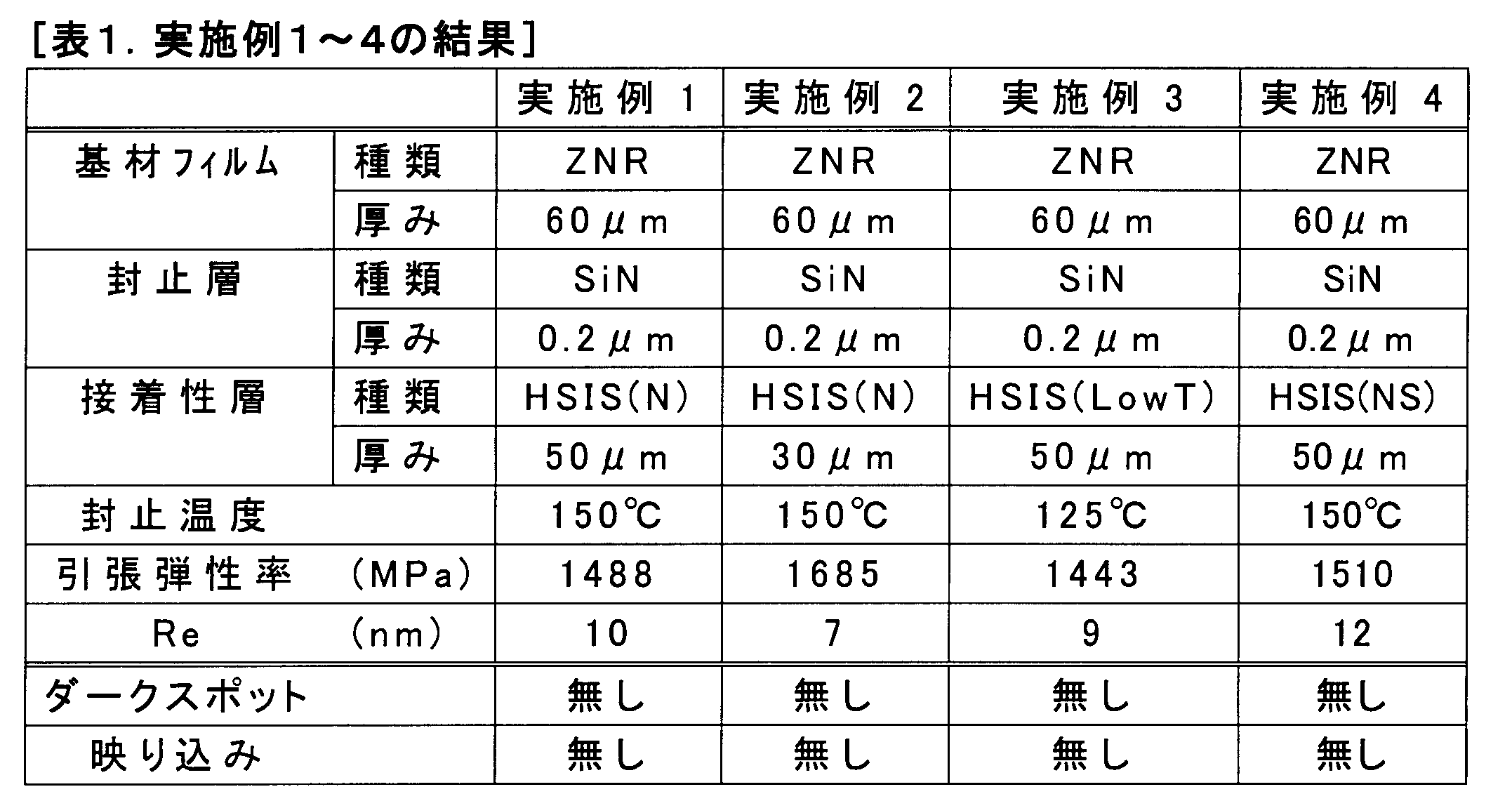
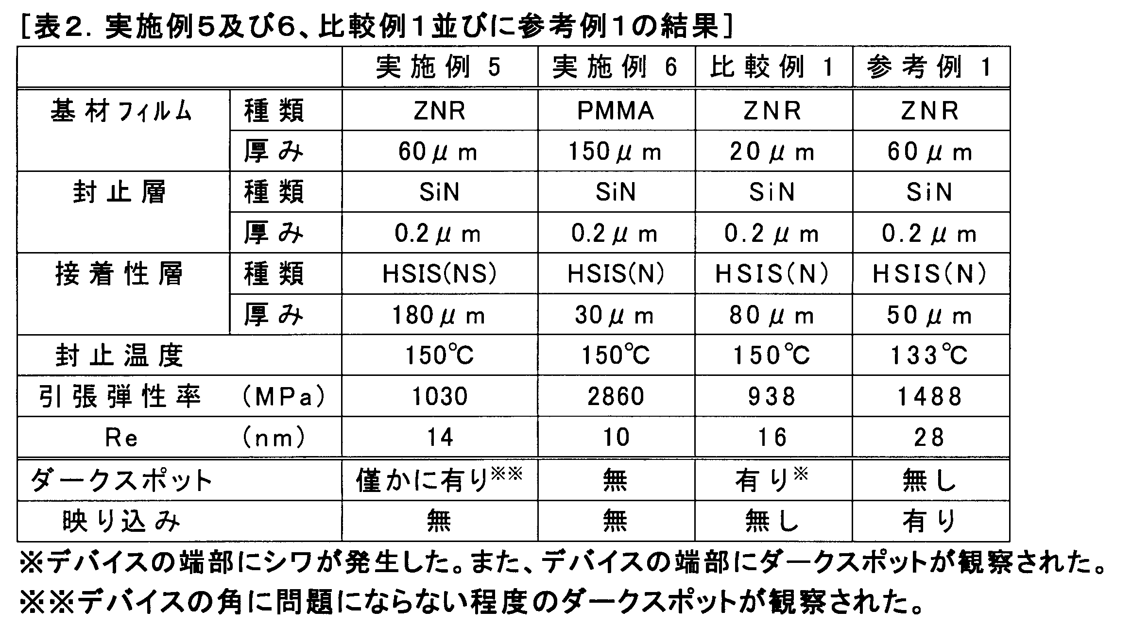
比較例1のように、引張り弾性率の低い封止フィルムでは、封止フィルムにコシが無く、シワが生じ易い。封止の際に微小なシワが生じると、そのシワに起因して構造体と封止フィルムと間に隙間ができる。その隙間に水及び酸素が浸入すると、素子を劣化するので、一部の素子の発光機能が低下してダークスポットが生じる。これに対し、実施例1~6においては、引張り弾性率が高くコシがある封止フィルムが得られているため、シワが生じにくい。よって、構造体を隙間無く封止できるので、ダークスポットの発生を防止できている。
110 基材フィルム
120 封止層
130 接着性層
200 有機EL表示装置
210 組立体
210U 組立体の上面
211 基板
211U 基板の上面
212 第一の電極層
213 エッジカバー層
214 発光層
215 第二の電極層
220 封止フィルム
221 基材フィルム
222 封止層
223 接着性層
224 封止フィルムの封止層及び接着性層からなる層部分
300 有機EL表示装置
310 反射防止フィルム
311 直線偏光板
312 1/4波長板
400 有機EL表示装置
420 封止フィルム
421 基材フィルム
500 有機EL表示装置
510 仮封止層
510U 仮封止層の上面
600 有機EL表示装置
610 吸着剤層
700 有機半導体デバイス
710 組立体
710U 組立体の上面
711 基板
712 ゲート電極
713 ゲート電極絶縁層
714 ソース電極
715 ドレイン電極
716 半導体層
800 構造体
Claims (6)
- 基材フィルム、封止層及び接着性層をこの順に備える封止フィルムであって、
前記封止フィルムが、1000MPa以上の引張り弾性率を有し、
封止後における前記封止フィルムの前記基材フィルムよりも前記封止層側に設けられた層部分のレターデーションが、20nm以下である、封止フィルム。 - 前記接着性層が、水添ブロック共重合体エラストマーを含む、請求項1記載の封止フィルム。
- 前記水添ブロック共重合体エラストマーが、ブロック共重合体の全不飽和結合の90%以上を水素化した水素化物であって、
前記ブロック共重合体は、芳香族ビニル化合物単位を主成分とする、共重合体1分子あたり2個以上の重合体ブロック[A]と、鎖状共役ジエン化合物単位を主成分とする、共重合体1分子あたり1個以上の重合体ブロック[B]とを有し、
前記ブロック共重合体全体に占める、全重合体ブロック[A]の重量分率wAと全重合体ブロック[B]の重量分率wBとの比(wA/wB)が20/80~60/40である、請求項2記載の封止フィルム。 - 前記基材フィルムが、脂環式オレフィン樹脂からなる、請求項1~3のいずれか一項に記載の封止フィルム。
- 請求項1~4のいずれか一項に記載の封止フィルムを備える、有機エレクトロルミネッセンス表示装置。
- 請求項1~4のいずれか一項に記載の封止フィルムを備える、有機半導体デバイス。
Priority Applications (5)
| Application Number | Priority Date | Filing Date | Title |
|---|---|---|---|
| JP2015555020A JP6524915B2 (ja) | 2013-12-26 | 2014-12-25 | 封止フィルム、有機エレクトロルミネッセンス表示装置及び有機半導体デバイス |
| EP14875321.3A EP3089551B1 (en) | 2013-12-26 | 2014-12-25 | Sealing film, organic electroluminescent display, and organic semiconductor device |
| CN201480068188.1A CN105830533B (zh) | 2013-12-26 | 2014-12-25 | 密封膜、有机场致发光显示装置及有机半导体器件 |
| US15/108,138 US10374190B2 (en) | 2013-12-26 | 2014-12-25 | Sealing film, organic electroluminescent display, and organic semiconductor device |
| KR1020167015871A KR102393258B1 (ko) | 2013-12-26 | 2014-12-25 | 봉지 필름, 유기 전기발광 표시장치 및 유기 반도체 디바이스 |
Applications Claiming Priority (2)
| Application Number | Priority Date | Filing Date | Title |
|---|---|---|---|
| JP2013-269726 | 2013-12-26 | ||
| JP2013269726 | 2013-12-26 |
Publications (1)
| Publication Number | Publication Date |
|---|---|
| WO2015099079A1 true WO2015099079A1 (ja) | 2015-07-02 |
Family
ID=53478922
Family Applications (1)
| Application Number | Title | Priority Date | Filing Date |
|---|---|---|---|
| PCT/JP2014/084389 Ceased WO2015099079A1 (ja) | 2013-12-26 | 2014-12-25 | 封止フィルム、有機エレクトロルミネッセンス表示装置及び有機半導体デバイス |
Country Status (7)
| Country | Link |
|---|---|
| US (1) | US10374190B2 (ja) |
| EP (1) | EP3089551B1 (ja) |
| JP (2) | JP6524915B2 (ja) |
| KR (1) | KR102393258B1 (ja) |
| CN (1) | CN105830533B (ja) |
| TW (1) | TWI664079B (ja) |
| WO (1) | WO2015099079A1 (ja) |
Cited By (15)
| Publication number | Priority date | Publication date | Assignee | Title |
|---|---|---|---|---|
| WO2017154718A1 (ja) * | 2016-03-09 | 2017-09-14 | 日本ゼオン株式会社 | 接合体、その製造方法、および変性ブロック共重合体水素化物からなるシート |
| WO2018021031A1 (ja) * | 2016-07-28 | 2018-02-01 | 日本ゼオン株式会社 | 熱可塑性エラストマー積層体及び有機エレクトロルミネッセンス装置 |
| WO2018043710A1 (ja) * | 2016-09-05 | 2018-03-08 | 住友化学株式会社 | 有機デバイスの製造方法 |
| WO2018056401A1 (ja) * | 2016-09-23 | 2018-03-29 | 凸版印刷株式会社 | ガスバリア性光学フィルム及び有機elディスプレイ |
| WO2019131457A1 (ja) * | 2017-12-26 | 2019-07-04 | 日本ゼオン株式会社 | 偏光板保護フィルム、偏光板及び表示装置 |
| JP2019188811A (ja) * | 2013-12-26 | 2019-10-31 | 日本ゼオン株式会社 | 封止フィルム、有機エレクトロルミネッセンス表示装置及び有機半導体デバイス |
| EP3480634A4 (en) * | 2016-06-30 | 2020-02-26 | Zeon Corporation | POLARIZING PLATE PROTECTIVE FILM, POLARIZING PLATE AND DISPLAY DEVICE |
| WO2020080202A1 (ja) | 2018-10-17 | 2020-04-23 | 日本ゼオン株式会社 | 共重合体水素化物およびその製造方法、共重合体水素化物含有組成物、合わせガラス用中間膜、合わせガラス用中間膜積層体、封止材、光学フィルム、医療用成形体およびその製造方法、接着剤、ならびに、接合体およびその製造方法 |
| EP3678172A4 (en) * | 2017-08-30 | 2021-04-21 | Zeon Corporation | LAMINATE AND METHOD FOR MANUFACTURING THEREOF |
| US11081672B2 (en) | 2017-02-23 | 2021-08-03 | Zeon Corporation | Resin film for electronic devices, and electronic device |
| WO2023120033A1 (ja) | 2021-12-24 | 2023-06-29 | 日本ゼオン株式会社 | 光電変換素子 |
| WO2023163023A1 (ja) | 2022-02-25 | 2023-08-31 | 日本ゼオン株式会社 | 組成物及びその製造方法、並びに組成物を含むフィルム、その用途、及びその製造方法 |
| US11970606B2 (en) | 2018-01-31 | 2024-04-30 | Zeon Corporation | Resin composition, resin film and organic electroluminescent device |
| US11976201B2 (en) | 2018-01-31 | 2024-05-07 | Zeon Corporation | Resin film and organic electroluminescent device |
| US12359078B2 (en) | 2019-06-14 | 2025-07-15 | Zeon Corporation | Resin solution for printing |
Families Citing this family (14)
| Publication number | Priority date | Publication date | Assignee | Title |
|---|---|---|---|---|
| TWI631743B (zh) * | 2015-11-24 | 2018-08-01 | 柯尼卡美能達股份有限公司 | Film sealing layer forming device |
| JP6809972B2 (ja) * | 2016-04-14 | 2021-01-06 | 住友化学株式会社 | 積層フィルム、積層フィルムの製造方法及びled搭載基板 |
| CN109890922A (zh) * | 2016-11-22 | 2019-06-14 | 日本瑞翁株式会社 | 卷状体 |
| KR101801690B1 (ko) | 2017-01-18 | 2017-11-27 | (주)이녹스첨단소재 | Oled 패널 하부 보호필름 및 이를 포함하는 oled 패널 |
| JP7137554B2 (ja) * | 2017-02-28 | 2022-09-14 | 日東電工株式会社 | 偏光板および偏光板の製造方法 |
| KR102530926B1 (ko) * | 2017-12-27 | 2023-05-09 | 엘지디스플레이 주식회사 | 지문 인식이 가능한 표시 장치 |
| KR102271843B1 (ko) * | 2017-12-18 | 2021-07-01 | 주식회사 엘지화학 | 봉지 필름 |
| EP3905227A4 (en) * | 2018-12-28 | 2022-09-28 | Agc Inc. | TRANSPARENT DISPLAY DEVICE AND MOBILE OBJECT |
| CN109713026B (zh) * | 2019-02-26 | 2024-09-20 | 京东方科技集团股份有限公司 | 一种硅基电致发光显示面板及其制造方法、显示装置 |
| KR102715321B1 (ko) * | 2019-04-24 | 2024-10-10 | 삼성디스플레이 주식회사 | 표시 장치 |
| CN113493555A (zh) * | 2020-04-01 | 2021-10-12 | 李长荣化学工业股份有限公司 | 苯乙烯-异戊二烯-苯乙烯三嵌段共聚物、其制造方法、及其组成物及黏着剂组合物 |
| CN111640373B (zh) * | 2020-06-09 | 2023-06-23 | 京东方科技集团股份有限公司 | 盖板和显示装置 |
| CN116235085A (zh) * | 2020-09-02 | 2023-06-06 | 富士胶片株式会社 | 液晶衍射元件、光学元件、图像显示单元、头戴式显示器、光束转向器及传感器 |
| KR102839164B1 (ko) * | 2021-10-28 | 2025-07-25 | 엘지디스플레이 주식회사 | 표시 장치 |
Citations (10)
| Publication number | Priority date | Publication date | Assignee | Title |
|---|---|---|---|---|
| JP2003163078A (ja) * | 2001-11-28 | 2003-06-06 | Hitachi Ltd | 表示装置 |
| JP2005129520A (ja) * | 2003-10-03 | 2005-05-19 | Jsr Corp | 有機el素子用透明封止材 |
| JP2009190186A (ja) | 2008-02-12 | 2009-08-27 | Gunze Ltd | ガスバリア層付フィルム |
| JP2010080293A (ja) * | 2008-09-26 | 2010-04-08 | Dainippon Printing Co Ltd | 有機エレクトロルミネッセンス素子封止用粘着フィルム |
| JP2012032418A (ja) | 2008-11-19 | 2012-02-16 | Sharp Corp | 円偏光板及び表示装置 |
| JP2013103373A (ja) * | 2011-11-11 | 2013-05-30 | Toyobo Co Ltd | 封止フィルム |
| WO2013084836A1 (ja) * | 2011-12-06 | 2013-06-13 | 株式会社ダイセル | シート状カバリング剤、カバリング方法又は電子デバイスの製造方法 |
| WO2013147093A1 (ja) * | 2012-03-30 | 2013-10-03 | リンテック株式会社 | ガスバリアフィルム積層体、電子デバイス用部材、及び電子デバイス |
| WO2014091941A1 (ja) * | 2012-12-10 | 2014-06-19 | 日本ゼオン株式会社 | 有機エレクトロニクスデバイス封止用樹脂組成物、及び有機エレクトロニクスデバイス |
| JP2014180794A (ja) * | 2013-03-19 | 2014-09-29 | Fujifilm Corp | 機能性フィルム |
Family Cites Families (13)
| Publication number | Priority date | Publication date | Assignee | Title |
|---|---|---|---|---|
| US4869966A (en) * | 1986-10-16 | 1989-09-26 | Shell Oil Company | Encapsulated assemblage and method of making |
| JP2006330604A (ja) * | 2005-05-30 | 2006-12-07 | Nippon Zeon Co Ltd | 積層構造体、位相差フィルム及び光学素子 |
| JP2010006039A (ja) * | 2007-09-05 | 2010-01-14 | Fujifilm Corp | ガスバリアフィルムおよびガスバリアフィルムを用いて表示素子を封止する方法。 |
| JP2009210789A (ja) | 2008-03-04 | 2009-09-17 | Nippon Zeon Co Ltd | 光学部材及び液晶表示装置 |
| JP5335483B2 (ja) * | 2009-02-27 | 2013-11-06 | リンテック株式会社 | 粘着剤層付き偏光板の製造方法 |
| JP2011180485A (ja) * | 2010-03-03 | 2011-09-15 | Seiko Epson Corp | 反射型液晶装置および電子機器 |
| KR101676313B1 (ko) * | 2010-05-31 | 2016-11-16 | 삼성디스플레이 주식회사 | 유기 발광 장치 |
| JP5807643B2 (ja) | 2010-09-29 | 2015-11-10 | 日本ゼオン株式会社 | アルコキシシリル基を有するブロック共重合体水素化物及びその利用 |
| EP2623526B1 (en) | 2010-09-29 | 2017-07-26 | Zeon Corporation | Hydrogenated block copolymer having alkoxysilyl group, and use therefor |
| JP5942222B2 (ja) * | 2010-12-15 | 2016-06-29 | 旭化成株式会社 | 光学部材用積層表面保護フィルム |
| KR101308480B1 (ko) | 2011-06-14 | 2013-09-16 | 엘지디스플레이 주식회사 | 플라스틱 유기 전계 발광 표시 장치 및 그 제조 방법 |
| JP6524915B2 (ja) * | 2013-12-26 | 2019-06-05 | 日本ゼオン株式会社 | 封止フィルム、有機エレクトロルミネッセンス表示装置及び有機半導体デバイス |
| US9871227B2 (en) * | 2014-07-31 | 2018-01-16 | Zeon Corporation | Light scattering layer having particles for an organic EL light emitting device |
-
2014
- 2014-12-25 JP JP2015555020A patent/JP6524915B2/ja active Active
- 2014-12-25 KR KR1020167015871A patent/KR102393258B1/ko active Active
- 2014-12-25 EP EP14875321.3A patent/EP3089551B1/en active Active
- 2014-12-25 WO PCT/JP2014/084389 patent/WO2015099079A1/ja not_active Ceased
- 2014-12-25 CN CN201480068188.1A patent/CN105830533B/zh active Active
- 2014-12-25 US US15/108,138 patent/US10374190B2/en active Active
- 2014-12-26 TW TW103145696A patent/TWI664079B/zh active
-
2019
- 2019-04-26 JP JP2019086561A patent/JP6673516B2/ja active Active
Patent Citations (10)
| Publication number | Priority date | Publication date | Assignee | Title |
|---|---|---|---|---|
| JP2003163078A (ja) * | 2001-11-28 | 2003-06-06 | Hitachi Ltd | 表示装置 |
| JP2005129520A (ja) * | 2003-10-03 | 2005-05-19 | Jsr Corp | 有機el素子用透明封止材 |
| JP2009190186A (ja) | 2008-02-12 | 2009-08-27 | Gunze Ltd | ガスバリア層付フィルム |
| JP2010080293A (ja) * | 2008-09-26 | 2010-04-08 | Dainippon Printing Co Ltd | 有機エレクトロルミネッセンス素子封止用粘着フィルム |
| JP2012032418A (ja) | 2008-11-19 | 2012-02-16 | Sharp Corp | 円偏光板及び表示装置 |
| JP2013103373A (ja) * | 2011-11-11 | 2013-05-30 | Toyobo Co Ltd | 封止フィルム |
| WO2013084836A1 (ja) * | 2011-12-06 | 2013-06-13 | 株式会社ダイセル | シート状カバリング剤、カバリング方法又は電子デバイスの製造方法 |
| WO2013147093A1 (ja) * | 2012-03-30 | 2013-10-03 | リンテック株式会社 | ガスバリアフィルム積層体、電子デバイス用部材、及び電子デバイス |
| WO2014091941A1 (ja) * | 2012-12-10 | 2014-06-19 | 日本ゼオン株式会社 | 有機エレクトロニクスデバイス封止用樹脂組成物、及び有機エレクトロニクスデバイス |
| JP2014180794A (ja) * | 2013-03-19 | 2014-09-29 | Fujifilm Corp | 機能性フィルム |
Non-Patent Citations (1)
| Title |
|---|
| See also references of EP3089551A4 |
Cited By (20)
| Publication number | Priority date | Publication date | Assignee | Title |
|---|---|---|---|---|
| JP2019188811A (ja) * | 2013-12-26 | 2019-10-31 | 日本ゼオン株式会社 | 封止フィルム、有機エレクトロルミネッセンス表示装置及び有機半導体デバイス |
| WO2017154718A1 (ja) * | 2016-03-09 | 2017-09-14 | 日本ゼオン株式会社 | 接合体、その製造方法、および変性ブロック共重合体水素化物からなるシート |
| US10816697B2 (en) | 2016-06-30 | 2020-10-27 | Zeon Corporation | Polarizing plate protective film, polarizing plate and display device |
| EP3480634A4 (en) * | 2016-06-30 | 2020-02-26 | Zeon Corporation | POLARIZING PLATE PROTECTIVE FILM, POLARIZING PLATE AND DISPLAY DEVICE |
| JPWO2018021031A1 (ja) * | 2016-07-28 | 2019-05-09 | 日本ゼオン株式会社 | 熱可塑性エラストマー積層体及び有機エレクトロルミネッセンス装置 |
| WO2018021031A1 (ja) * | 2016-07-28 | 2018-02-01 | 日本ゼオン株式会社 | 熱可塑性エラストマー積層体及び有機エレクトロルミネッセンス装置 |
| CN109476127A (zh) * | 2016-07-28 | 2019-03-15 | 日本瑞翁株式会社 | 热塑性弹性体层叠体和有机电致发光装置 |
| WO2018043710A1 (ja) * | 2016-09-05 | 2018-03-08 | 住友化学株式会社 | 有機デバイスの製造方法 |
| WO2018056401A1 (ja) * | 2016-09-23 | 2018-03-29 | 凸版印刷株式会社 | ガスバリア性光学フィルム及び有機elディスプレイ |
| US11081672B2 (en) | 2017-02-23 | 2021-08-03 | Zeon Corporation | Resin film for electronic devices, and electronic device |
| EP3678172A4 (en) * | 2017-08-30 | 2021-04-21 | Zeon Corporation | LAMINATE AND METHOD FOR MANUFACTURING THEREOF |
| US11440303B2 (en) | 2017-08-30 | 2022-09-13 | Zeon Corporation | Laminate and method of manufacturing same |
| WO2019131457A1 (ja) * | 2017-12-26 | 2019-07-04 | 日本ゼオン株式会社 | 偏光板保護フィルム、偏光板及び表示装置 |
| US11970606B2 (en) | 2018-01-31 | 2024-04-30 | Zeon Corporation | Resin composition, resin film and organic electroluminescent device |
| US11976201B2 (en) | 2018-01-31 | 2024-05-07 | Zeon Corporation | Resin film and organic electroluminescent device |
| WO2020080202A1 (ja) | 2018-10-17 | 2020-04-23 | 日本ゼオン株式会社 | 共重合体水素化物およびその製造方法、共重合体水素化物含有組成物、合わせガラス用中間膜、合わせガラス用中間膜積層体、封止材、光学フィルム、医療用成形体およびその製造方法、接着剤、ならびに、接合体およびその製造方法 |
| US11773193B2 (en) | 2018-10-17 | 2023-10-03 | Zeon Corporation | Hydrogenated copolymer and method of producing the same, hydrogenated copolymer-containing composition, interlayer film for laminated glass, interlayer film laminate for laminated glass, sealing material, optical film, medical shaped article and method of producing the same, adhesive, and assembly and method of producing the same |
| US12359078B2 (en) | 2019-06-14 | 2025-07-15 | Zeon Corporation | Resin solution for printing |
| WO2023120033A1 (ja) | 2021-12-24 | 2023-06-29 | 日本ゼオン株式会社 | 光電変換素子 |
| WO2023163023A1 (ja) | 2022-02-25 | 2023-08-31 | 日本ゼオン株式会社 | 組成物及びその製造方法、並びに組成物を含むフィルム、その用途、及びその製造方法 |
Also Published As
| Publication number | Publication date |
|---|---|
| EP3089551B1 (en) | 2020-04-15 |
| TWI664079B (zh) | 2019-07-01 |
| JP6524915B2 (ja) | 2019-06-05 |
| KR102393258B1 (ko) | 2022-04-29 |
| JP6673516B2 (ja) | 2020-03-25 |
| CN105830533B (zh) | 2018-06-01 |
| US10374190B2 (en) | 2019-08-06 |
| TW201529315A (zh) | 2015-08-01 |
| JPWO2015099079A1 (ja) | 2017-03-23 |
| CN105830533A (zh) | 2016-08-03 |
| EP3089551A4 (en) | 2017-08-09 |
| US20160343970A1 (en) | 2016-11-24 |
| JP2019188811A (ja) | 2019-10-31 |
| EP3089551A1 (en) | 2016-11-02 |
| KR20160102181A (ko) | 2016-08-29 |
Similar Documents
| Publication | Publication Date | Title |
|---|---|---|
| JP6673516B2 (ja) | 封止フィルム、有機エレクトロルミネッセンス表示装置及び有機半導体デバイス | |
| CN104854190B (zh) | 有机电子器件密封用树脂组合物及有机电子器件 | |
| CN104619485B (zh) | 复合阻气叠层体及其制造方法、以及复合电极 | |
| CN105917737B (zh) | 复合阻气叠层体及其制造方法 | |
| WO2016153030A1 (ja) | 封止材、封止材の製造方法、及び、発光装置の製造方法 | |
| JP6638350B2 (ja) | 複合ガスバリア積層体及び有機エレクトロルミネッセンス発光体 |
Legal Events
| Date | Code | Title | Description |
|---|---|---|---|
| 121 | Ep: the epo has been informed by wipo that ep was designated in this application |
Ref document number: 14875321 Country of ref document: EP Kind code of ref document: A1 |
|
| ENP | Entry into the national phase |
Ref document number: 2015555020 Country of ref document: JP Kind code of ref document: A |
|
| ENP | Entry into the national phase |
Ref document number: 20167015871 Country of ref document: KR Kind code of ref document: A |
|
| WWE | Wipo information: entry into national phase |
Ref document number: 15108138 Country of ref document: US |
|
| NENP | Non-entry into the national phase |
Ref country code: DE |
|
| REEP | Request for entry into the european phase |
Ref document number: 2014875321 Country of ref document: EP |
|
| WWE | Wipo information: entry into national phase |
Ref document number: 2014875321 Country of ref document: EP |