WO2015093300A1 - 圧電振動デバイス - Google Patents
圧電振動デバイス Download PDFInfo
- Publication number
- WO2015093300A1 WO2015093300A1 PCT/JP2014/082105 JP2014082105W WO2015093300A1 WO 2015093300 A1 WO2015093300 A1 WO 2015093300A1 JP 2014082105 W JP2014082105 W JP 2014082105W WO 2015093300 A1 WO2015093300 A1 WO 2015093300A1
- Authority
- WO
- WIPO (PCT)
- Prior art keywords
- bonding pattern
- sealing
- vibration
- bonding
- sealing member
- Prior art date
Links
- 230000010355 oscillation Effects 0.000 title claims abstract description 26
- 238000007789 sealing Methods 0.000 claims abstract description 645
- 238000009792 diffusion process Methods 0.000 claims abstract description 114
- 238000005240 physical vapour deposition Methods 0.000 claims description 355
- 230000005284 excitation Effects 0.000 claims description 223
- 239000000463 material Substances 0.000 claims description 100
- 238000005304 joining Methods 0.000 claims description 78
- 229910052751 metal Inorganic materials 0.000 claims description 77
- 239000002184 metal Substances 0.000 claims description 77
- 239000000758 substrate Substances 0.000 claims description 44
- 238000005452 bending Methods 0.000 claims description 14
- 239000013078 crystal Substances 0.000 abstract description 301
- 239000010408 film Substances 0.000 description 293
- 239000010453 quartz Substances 0.000 description 39
- VYPSYNLAJGMNEJ-UHFFFAOYSA-N silicon dioxide Inorganic materials O=[Si]=O VYPSYNLAJGMNEJ-UHFFFAOYSA-N 0.000 description 39
- 238000000605 extraction Methods 0.000 description 38
- 239000003566 sealing material Substances 0.000 description 35
- 239000011521 glass Substances 0.000 description 23
- 229910000679 solder Inorganic materials 0.000 description 23
- 238000004519 manufacturing process Methods 0.000 description 18
- 238000000034 method Methods 0.000 description 18
- 238000010438 heat treatment Methods 0.000 description 14
- 238000007740 vapor deposition Methods 0.000 description 14
- 230000009467 reduction Effects 0.000 description 12
- 238000007747 plating Methods 0.000 description 11
- 229910015363 Au—Sn Inorganic materials 0.000 description 10
- 239000004593 Epoxy Substances 0.000 description 9
- 239000012530 fluid Substances 0.000 description 9
- 238000002844 melting Methods 0.000 description 9
- 230000000694 effects Effects 0.000 description 8
- 238000007689 inspection Methods 0.000 description 8
- 238000010030 laminating Methods 0.000 description 8
- 230000004048 modification Effects 0.000 description 8
- 238000012986 modification Methods 0.000 description 8
- 230000008569 process Effects 0.000 description 8
- 238000001953 recrystallisation Methods 0.000 description 8
- 230000007547 defect Effects 0.000 description 7
- 230000008018 melting Effects 0.000 description 7
- 238000010586 diagram Methods 0.000 description 6
- 238000000059 patterning Methods 0.000 description 6
- 230000002093 peripheral effect Effects 0.000 description 6
- 239000010953 base metal Substances 0.000 description 5
- 238000007796 conventional method Methods 0.000 description 5
- 230000003746 surface roughness Effects 0.000 description 5
- 239000000853 adhesive Substances 0.000 description 4
- 230000001070 adhesive effect Effects 0.000 description 4
- 239000011230 binding agent Substances 0.000 description 4
- 230000015572 biosynthetic process Effects 0.000 description 4
- 230000008859 change Effects 0.000 description 4
- 239000000470 constituent Substances 0.000 description 4
- 238000002425 crystallisation Methods 0.000 description 4
- 230000008025 crystallization Effects 0.000 description 4
- 230000006866 deterioration Effects 0.000 description 4
- 238000007733 ion plating Methods 0.000 description 4
- 238000000608 laser ablation Methods 0.000 description 4
- 239000012528 membrane Substances 0.000 description 4
- 238000001451 molecular beam epitaxy Methods 0.000 description 4
- 230000000149 penetrating effect Effects 0.000 description 4
- 238000000206 photolithography Methods 0.000 description 4
- 230000007261 regionalization Effects 0.000 description 4
- 238000004544 sputter deposition Methods 0.000 description 4
- 238000001771 vacuum deposition Methods 0.000 description 4
- 238000009826 distribution Methods 0.000 description 3
- 239000012780 transparent material Substances 0.000 description 3
- WSMQKESQZFQMFW-UHFFFAOYSA-N 5-methyl-pyrazole-3-carboxylic acid Chemical compound CC1=CC(C(O)=O)=NN1 WSMQKESQZFQMFW-UHFFFAOYSA-N 0.000 description 2
- 229910017944 Ag—Cu Inorganic materials 0.000 description 2
- 229910000881 Cu alloy Inorganic materials 0.000 description 2
- 238000005229 chemical vapour deposition Methods 0.000 description 2
- 230000008878 coupling Effects 0.000 description 2
- 238000010168 coupling process Methods 0.000 description 2
- 238000005859 coupling reaction Methods 0.000 description 2
- 238000007772 electroless plating Methods 0.000 description 2
- 238000009713 electroplating Methods 0.000 description 2
- 230000005496 eutectics Effects 0.000 description 2
- 230000004927 fusion Effects 0.000 description 2
- 229910052737 gold Inorganic materials 0.000 description 2
- GQYHUHYESMUTHG-UHFFFAOYSA-N lithium niobate Chemical compound [Li+].[O-][Nb](=O)=O GQYHUHYESMUTHG-UHFFFAOYSA-N 0.000 description 2
- 239000007769 metal material Substances 0.000 description 2
- 229910052759 nickel Inorganic materials 0.000 description 2
- 238000007639 printing Methods 0.000 description 2
- 239000000126 substance Substances 0.000 description 2
- 230000001629 suppression Effects 0.000 description 2
- 239000000919 ceramic Substances 0.000 description 1
- 239000004020 conductor Substances 0.000 description 1
- 229910052802 copper Inorganic materials 0.000 description 1
- 238000005336 cracking Methods 0.000 description 1
- 230000007423 decrease Effects 0.000 description 1
- 230000009969 flowable effect Effects 0.000 description 1
- 230000007257 malfunction Effects 0.000 description 1
- 230000035515 penetration Effects 0.000 description 1
- 239000012071 phase Substances 0.000 description 1
- 238000007781 pre-processing Methods 0.000 description 1
- 238000003825 pressing Methods 0.000 description 1
- 238000005476 soldering Methods 0.000 description 1
- 230000000087 stabilizing effect Effects 0.000 description 1
- 239000010409 thin film Substances 0.000 description 1
- 238000001947 vapour-phase growth Methods 0.000 description 1
- 238000004804 winding Methods 0.000 description 1
Images


Classifications
-
- H—ELECTRICITY
- H03—ELECTRONIC CIRCUITRY
- H03H—IMPEDANCE NETWORKS, e.g. RESONANT CIRCUITS; RESONATORS
- H03H3/00—Apparatus or processes specially adapted for the manufacture of impedance networks, resonating circuits, resonators
- H03H3/007—Apparatus or processes specially adapted for the manufacture of impedance networks, resonating circuits, resonators for the manufacture of electromechanical resonators or networks
- H03H3/02—Apparatus or processes specially adapted for the manufacture of impedance networks, resonating circuits, resonators for the manufacture of electromechanical resonators or networks for the manufacture of piezoelectric or electrostrictive resonators or networks
-
- H—ELECTRICITY
- H03—ELECTRONIC CIRCUITRY
- H03H—IMPEDANCE NETWORKS, e.g. RESONANT CIRCUITS; RESONATORS
- H03H9/00—Networks comprising electromechanical or electro-acoustic devices; Electromechanical resonators
- H03H9/02—Details
- H03H9/05—Holders; Supports
- H03H9/0538—Constructional combinations of supports or holders with electromechanical or other electronic elements
- H03H9/0547—Constructional combinations of supports or holders with electromechanical or other electronic elements consisting of a vertical arrangement
- H03H9/0561—Constructional combinations of supports or holders with electromechanical or other electronic elements consisting of a vertical arrangement consisting of a multilayered structure
-
- H—ELECTRICITY
- H03—ELECTRONIC CIRCUITRY
- H03H—IMPEDANCE NETWORKS, e.g. RESONANT CIRCUITS; RESONATORS
- H03H9/00—Networks comprising electromechanical or electro-acoustic devices; Electromechanical resonators
- H03H9/02—Details
- H03H9/05—Holders; Supports
- H03H9/10—Mounting in enclosures
- H03H9/1007—Mounting in enclosures for bulk acoustic wave [BAW] devices
- H03H9/1035—Mounting in enclosures for bulk acoustic wave [BAW] devices the enclosure being defined by two sealing substrates sandwiching the piezoelectric layer of the BAW device
-
- H—ELECTRICITY
- H03—ELECTRONIC CIRCUITRY
- H03H—IMPEDANCE NETWORKS, e.g. RESONANT CIRCUITS; RESONATORS
- H03H9/00—Networks comprising electromechanical or electro-acoustic devices; Electromechanical resonators
- H03H9/02—Details
- H03H9/125—Driving means, e.g. electrodes, coils
- H03H9/13—Driving means, e.g. electrodes, coils for networks consisting of piezoelectric or electrostrictive materials
- H03H9/131—Driving means, e.g. electrodes, coils for networks consisting of piezoelectric or electrostrictive materials consisting of a multilayered structure
-
- H—ELECTRICITY
- H03—ELECTRONIC CIRCUITRY
- H03H—IMPEDANCE NETWORKS, e.g. RESONANT CIRCUITS; RESONATORS
- H03H9/00—Networks comprising electromechanical or electro-acoustic devices; Electromechanical resonators
- H03H9/15—Constructional features of resonators consisting of piezoelectric or electrostrictive material
- H03H9/17—Constructional features of resonators consisting of piezoelectric or electrostrictive material having a single resonator
-
- H—ELECTRICITY
- H01—ELECTRIC ELEMENTS
- H01L—SEMICONDUCTOR DEVICES NOT COVERED BY CLASS H10
- H01L2224/00—Indexing scheme for arrangements for connecting or disconnecting semiconductor or solid-state bodies and methods related thereto as covered by H01L24/00
- H01L2224/01—Means for bonding being attached to, or being formed on, the surface to be connected, e.g. chip-to-package, die-attach, "first-level" interconnects; Manufacturing methods related thereto
- H01L2224/10—Bump connectors; Manufacturing methods related thereto
- H01L2224/15—Structure, shape, material or disposition of the bump connectors after the connecting process
- H01L2224/16—Structure, shape, material or disposition of the bump connectors after the connecting process of an individual bump connector
- H01L2224/161—Disposition
- H01L2224/16151—Disposition the bump connector connecting between a semiconductor or solid-state body and an item not being a semiconductor or solid-state body, e.g. chip-to-substrate, chip-to-passive
- H01L2224/16221—Disposition the bump connector connecting between a semiconductor or solid-state body and an item not being a semiconductor or solid-state body, e.g. chip-to-substrate, chip-to-passive the body and the item being stacked
- H01L2224/16225—Disposition the bump connector connecting between a semiconductor or solid-state body and an item not being a semiconductor or solid-state body, e.g. chip-to-substrate, chip-to-passive the body and the item being stacked the item being non-metallic, e.g. insulating substrate with or without metallisation
-
- H—ELECTRICITY
- H03—ELECTRONIC CIRCUITRY
- H03H—IMPEDANCE NETWORKS, e.g. RESONANT CIRCUITS; RESONATORS
- H03H9/00—Networks comprising electromechanical or electro-acoustic devices; Electromechanical resonators
- H03H9/02—Details
- H03H9/05—Holders; Supports
- H03H9/10—Mounting in enclosures
- H03H9/1007—Mounting in enclosures for bulk acoustic wave [BAW] devices
- H03H9/1014—Mounting in enclosures for bulk acoustic wave [BAW] devices the enclosure being defined by a frame built on a substrate and a cap, the frame having no mechanical contact with the BAW device
- H03H9/1021—Mounting in enclosures for bulk acoustic wave [BAW] devices the enclosure being defined by a frame built on a substrate and a cap, the frame having no mechanical contact with the BAW device the BAW device being of the cantilever type
Definitions
- the present invention relates to a piezoelectric vibration device.
- piezoelectric vibration devices for example, crystal resonators
- the casing is composed of a rectangular parallelepiped package.
- This package is composed of a first sealing member and a second sealing member made of glass, and a crystal vibrating plate made of crystal and having excitation electrodes formed on both main surfaces.
- the first sealing member and the second sealing member A stop member is laminated and bonded via a quartz diaphragm, and the excitation electrode of the quartz diaphragm disposed inside the package is hermetically sealed (for example, Patent Document 1).
- a sandwich structure such a laminated form of piezoelectric vibration devices is referred to as a sandwich structure.
- a metal paste sealing material is used for joining the first sealing member, the second sealing member, and the crystal diaphragm.
- the metal paste sealing material here is thicker than an electrode film and is not suitable for lowering the height. Further, in the case of joining using a metal paste sealing material, it is always heated and melted at a high temperature, and gas is generated during heating and melting. The presence of this gas inside the package degrades the vibration characteristics. Furthermore, since the metal paste sealing material is formed on a quartz diaphragm or the like in a wide shape, it is necessary to secure a region for arranging the metal paste sealing material, which hinders the downsizing of the package.
- an object of the present invention is to provide a piezoelectric vibration device having a sandwich structure that eliminates the generation of gas and can be reduced in height and size.
- a first excitation electrode is formed on one main surface of a substrate, and a second excitation that is paired with the first excitation electrode on the other main surface of the substrate.
- one main surface of the piezoelectric diaphragm has the first surface on the first surface.
- a vibration-side first bonding pattern for bonding to a sealing member is formed, and the vibration The first bonding pattern includes a base PVD film formed by physical vapor deposition on the one main surface, and an electrode PVD film formed by physical vapor deposition on the base PVD film.
- a vibration side second bonding pattern for bonding to the second sealing member is formed on the other main surface of the piezoelectric diaphragm, and the vibration side second bonding pattern is physically formed on the other main surface.
- the first PVD film includes a base PVD film formed by vapor phase growth and an electrode PVD film formed by physical vapor deposition on the base PVD film, and the piezoelectric sealing plate includes the first sealing member.
- a sealing-side first bonding pattern for bonding to the substrate, and the sealing-side first bonding pattern includes a base PVD film formed by physical vapor deposition on the first sealing member; Electrode PV laminated by physical vapor deposition on the underlying PVD film The second sealing member is formed with a sealing-side second bonding pattern for bonding to the piezoelectric diaphragm, and the sealing-side second bonding pattern is formed by the second sealing member.
- the vibration side first bonding pattern is diffusion bonded, and the sealing side second bonding pattern and the vibration side second bonding pattern are diffusion bonded.
- the piezoelectric vibration device in the piezoelectric vibration device having a sandwich structure, the generation of gas is eliminated, and the height and size can be further reduced.
- the sealing side first bonding pattern and the vibration side first bonding pattern are used.
- the sealing-side second bonding pattern and the vibration-side second bonding pattern are diffusion-bonded, so that it is not necessary to use a metal paste sealing material separately, which contributes to cost reduction. It becomes possible.
- the underlying PVD film or the electrode PVD film is formed by a PVD method such as vacuum deposition, sputtering, ion plating, MBE, or laser ablation (for example, a film forming method for patterning in processing such as photolithography). Since the film is formed, it is possible to reduce the number of manufacturing steps and contribute to the cost reduction by collectively forming the film, unlike the case of forming the film multiple times using the conventional plating.
- the package of the piezoelectric vibration device is currently being downsized. For this reason, while preventing a problem such as a short circuit due to interference of patterns (electrode patterns) and terminals (electrode pads) having different polarities, Au- It is difficult to print a metal paste sealing material such as Sn.
- the sealing side first and second bonding patterns and the vibration side each of which has a laminated structure of the base PVD film and the electrode PVD film, respectively. Since the first and second bonding patterns are used, it is possible to form a pattern while preventing problems such as short-circuiting due to interference between patterns and terminals having different polarities.
- a metal paste sealing material such as Au—Sn is separately used, but in the case of joining using this metal paste sealing material, it is always heated at a high temperature for fusion joining. And gas is generated during heat-melting. A technique for eliminating this gas has not been developed at present, and gas intrusion into the internal space is unavoidable during heat-melt bonding.
- the sealing side first bonding pattern and the vibration side first bonding pattern are diffusion bonded, and the sealing side second bonding pattern and the vibration side second bonding pattern are Since diffusion bonding is performed, it is possible to suppress the generation of gas and to prevent deterioration of vibration characteristics due to the presence of gas in the internal space.
- a temperature higher than room temperature such as 220 ° C. may be applied, but applying a high temperature (for example, 280 ° C. or more) as in the bonding using the metal paste sealing material is not possible. Absent.
- the sealing side first and second bonding patterns and the vibration side first and second bonding patterns each have a laminated structure of the base PVD film and the electrode PVD film. It is possible to reduce the width of terminals and terminals to make them thinner, and as a result, it is possible to eliminate the hindrance to downsizing of the package caused by the pattern routing. Specifically, according to the present invention, it is possible to make patterns and terminals thin, which cannot be realized with a piezoelectric vibration device using bonding with a metal paste sealing material such as Au—Sn.
- the sealing side first bonding pattern and the vibration side first bonding pattern are diffusion bonded, and the sealing side second bonding pattern and the vibration side second bonding pattern are diffusion bonded. Therefore, high-temperature heat-melt joining is not performed. For this reason, when the piezoelectric vibration device is bonded to an external member such as an external circuit using solder or the like, it is not remelted at the bonding portion, and the bonding state does not change in a reflow or product use environment.
- the sealing side first bonding pattern and the vibration side first bonding pattern are bonded at room temperature by diffusion, and the sealing side second bonding pattern and the vibration side second bonding pattern are bonded at room temperature by diffusion bonding. Also good.
- the sealing-side first bonding pattern and the vibration-side first bonding pattern are bonded at room temperature
- the sealing-side second bonding pattern and the vibration-side second bonding pattern are bonded at room temperature. It is suitable for suppressing the generation of gas and preventing deterioration of vibration characteristics due to the presence of gas in the internal space. Moreover, it does not remelt at the joining location, and the joining state does not change.
- the said structure WHEREIN The said sealing side 1st joining pattern and the said vibration side 1st joining pattern are diffusion-bonded at the temperature below normal temperature or more and less than 230 degreeC, and the said sealing side 2nd joining pattern and the said vibration side 2nd The bonding pattern may be diffusion bonded at a temperature not lower than room temperature and lower than 230 ° C.
- the sealing-side first bonding pattern and the vibration-side first bonding pattern are diffusion-bonded at a temperature of normal temperature or higher and lower than 230 ° C.
- the sealing-side second bonding pattern and the vibration-side second bonding pattern are Are diffusion-bonded at a temperature not lower than room temperature and lower than 230 ° C. Therefore, it is possible to improve the bonding while suppressing the generation of gas.
- the said structure WHEREIN The said 1st excitation electrode formed in the one main surface of the said piezoelectric diaphragm and the said vibration side 1st joining pattern have the same thickness, The said 1st excitation electrode and the said vibration side 1st joining pattern And the second excitation electrode formed on the other main surface of the piezoelectric diaphragm and the vibration-side second bonding pattern have the same thickness, and the second excitation electrode and the vibration The surface of the second side bonding pattern may be made of the same metal.
- the first excitation electrode formed on one main surface of the piezoelectric diaphragm and the vibration-side first bonding pattern have the same thickness, and the surfaces of the first excitation electrode and the vibration-side first bonding pattern are
- the second excitation electrode and the vibration side second bonding pattern made of the same metal and formed on the other main surface of the piezoelectric diaphragm have the same thickness, and the second excitation electrode and the vibration side second bonding are Since the surface of the pattern is made of the same metal, it is possible to form the metal film of the first excitation electrode and the vibration side first bonding pattern only once, and the second excitation electrode and the vibration side first electrode are formed. It is possible to form the metal film with the two junction pattern only once. As a result, the metal film of the first excitation electrode and the vibration side first bonding pattern can be made the same, and the metal film of the second excitation electrode and the vibration side second bonding pattern can be made the same. .
- membrane The electrode PVD film may be thicker than the electrode PVD film.
- an outer main surface that does not face the piezoelectric diaphragm is formed with an external terminal for electrical connection to the outside, and the external terminal is
- the vibration-side first bonding pattern comprises: a base PVD film formed by physical vapor deposition on the principal surface of the electrode; and an electrode PVD film formed by physical vapor deposition on the base PVD film and laminated.
- the thickness of the base PVD film of the external terminal with respect to the thickness of the base PVD film of the vibration side second joint pattern, the sealing side first joint pattern, and the sealing side second joint pattern. It may be thick.
- each base PVD film of the vibration side first bonding pattern, the vibration side second bonding pattern, the sealing side first bonding pattern, and the sealing side second bonding pattern Since the base PVD film is thick, the external terminals are electrically connected to the outside while stabilizing the bonding of the first sealing member, the second sealing member, and the piezoelectric diaphragm (for example, , Solder mounting, etc.), it is possible to effectively use the underlying PVD film to electrically connect to the outside.
- the thickness of each base PVD film of the vibration side first bonding pattern, the vibration side second bonding pattern, the sealing side first bonding pattern, the sealing side second bonding pattern, and the external terminal is the same. In this case, electrical connection (for example, solder mounting) with the outside using the external terminal cannot be performed.
- Au may be used for the electrode PVD film.
- each surface of the vibration side first bonding pattern, the vibration side second bonding pattern, the sealing side first bonding pattern, and the sealing side second bonding pattern is oxidized. And no special special pretreatment is required for pretreatment of joining the vibration side first joining pattern, the vibration side second joining pattern, the sealing side first joining pattern, and the sealing side second joining pattern. It becomes. As a result, the manufacturing cost can be suppressed.
- the atmosphere environment does not have to be an ultra-high vacuum, for example.
- the vibration side first bonding pattern, the vibration side second bonding pattern, the sealing side first bonding pattern, and the sealing side second bonding pattern may be non-Sn patterns.
- vibration side first bonding pattern, the vibration side second bonding pattern, the sealing side first bonding pattern, and the sealing side second bonding pattern are non-Sn patterns, high temperature heating is not required during bonding. There is no problem (remelting) due to high-temperature heat bonding.
- the underlying PVD film or the electrode PVD film is formed by a PVD method such as vacuum deposition, sputtering, ion plating, MBE, or laser ablation (for example, a film forming method for patterning in processing such as photolithography). Since it forms, it can contribute to cost reduction.
- a PVD method such as vacuum deposition, sputtering, ion plating, MBE, or laser ablation (for example, a film forming method for patterning in processing such as photolithography). Since it forms, it can contribute to cost reduction.
- the pattern can be thinned, and a defect such as a short circuit due to interference of patterns or terminals having different polarities does not occur.
- Cu may be contained in the vibration side first bonding pattern, the vibration side second bonding pattern, the sealing side first bonding pattern, and the sealing side second bonding pattern.
- the vibration-side first bonding pattern, the vibration-side second bonding pattern, the sealing-side first bonding pattern, and the sealing-side second bonding pattern contain Cu, at the time of manufacturing (bonding, pressurization) It is possible to contribute to stress relaxation at the time of impact due to the occurrence of external force such as) and during use (at the time of impact due to the occurrence of external force such as dropping, solder mounting, etc.). That is, according to this configuration, the mechanical strength is improved.
- Cr is used for the base PVD film (for example, Cr + Ag-Cu + Au), it is suitable for resistance heating vapor deposition.
- the sealing side first bonding pattern and the vibration side first bonding pattern are pressure diffusion bonded
- the sealing side second bonding pattern and the vibration side second bonding pattern are pressure diffusion bonding. May be.
- the sealing side first bonding pattern and the vibration side first bonding pattern are pressure diffusion bonded, and the sealing side second bonding pattern and the vibration side second bonding pattern are pressed. Since diffusion bonding is performed, it becomes easy to secure a bonding portion by applying pressure, and it becomes possible to perform bonding by diffusion bonding alone more favorably without using high-temperature heating.
- the first sealing member and the second sealing member may be made of a material having a bending stiffness (secondary moment of section ⁇ Young's modulus) of 1000 [N ⁇ mm 2 ] or less.
- first sealing member and the second sealing member are made of an insulating (brittle) material having a bending rigidity (secondary moment of section ⁇ Young's modulus) of 1000 [N ⁇ mm 2 ] or less. It is possible to satisfy the amount of deformation required for. Therefore, for example, the bending rigidity within the above range can be obtained without forming the electrode surfaces such as the first excitation electrode and the second excitation electrode to have a surface roughness (Ra) of 1 nm or less necessary for normal bonding. By doing so, diffusion bonding can be performed.
- a surface roughness
- the sealing-side first bonding pattern and the vibration-side first bonding pattern are pressure-diffusion bonded without using a dedicated bonding material such as an adhesive, and the sealing-side second bonding pattern
- the vibration side second bonding pattern may be pressure diffusion bonded.
- the sealing-side first bonding pattern and the vibration-side first bonding pattern are pressure diffusion bonded without using a separate bonding-dedicated material, and the sealing-side second bonding pattern and the vibration-side second bonding pattern are Since pressure diffusion bonding is used, it is possible to contribute to downsizing, especially low profile, and when using a dedicated joint material, there is a limit to low profile, but low profile exceeding this limit is achieved. Is possible.
- an outer main surface that does not face the piezoelectric diaphragm is formed with an external terminal for electrical connection to the outside, and the external terminal is connected to the outer side.
- a primary PVD film formed by physical vapor deposition on the main surface of the electrode, and an electrode PVD film formed by physical vapor deposition on the underlying PVD film, and the sealing side first junction The thickness of the bonding pattern in which the pattern and the vibration side first bonding pattern are diffusion bonded is the same as the thickness of the bonding pattern in which the sealing side second bonding pattern and the vibration side second bonding pattern are diffusion bonded.
- the thickness of the external terminal electrically connected to the outside may be different.
- the base PVD film can be effectively used to electrically connect to the outside.
- the second sealing member may be formed with a through-hole disposed outside the internal space, and the through-hole may not be formed inside the internal space.
- the through hole disposed outside the internal space is formed, the through hole is inward of the internal space without the influence of the through hole reaching the internal space. Compared with the configuration arranged in the above, it is possible to avoid airtight defects caused by the through-holes.
- the through hole when the through hole is arranged in the internal space, it is necessary to ensure the air tightness of the internal space, and a process of filling the through hole in the internal space with a metal or the like is required.
- the vibration side first bonding pattern, the vibration side second bonding pattern, and the sealing side first bonding pattern are formed.
- the wiring pattern can be routed in the same process as the pattern formation with the sealing-side second bonding pattern, and the manufacturing cost can be reduced.
- the said structure WHEREIN The said sealing side 1st joining pattern formed in the said 1st sealing member and the said sealing side 2nd joining pattern formed in the said 2nd sealing member overlap in planar view. It does not have to be.
- sealing side first bonding pattern and the sealing side second bonding pattern do not overlap in plan view, stray capacitance is generated by the sealing side first bonding pattern and the sealing side second bonding pattern. Can be prevented.
- the vibration side first joining pattern and the vibration side second joining for sealingly joining the first sealing member and the second sealing member to the one principal surface and the other principal surface of the piezoelectric diaphragm.
- the sealing side first joint formed on the first sealing member in comparison with the vibration side first joint pattern and the vibration side second joint pattern formed on the piezoelectric diaphragm, respectively.
- the width of the pattern and the sealing-side second bonding pattern formed on the second sealing member may be wide.
- the width of the bonding pattern between the vibration side first bonding pattern and the vibration side second bonding pattern becomes narrow.
- the bonding pattern of the sealing-side first bonding pattern and the sealing-side second bonding pattern It is possible to widen the width, and as a result, it is possible to increase the degree of freedom in alignment accuracy during bonding.
- an oscillation circuit element may be provided on one main surface, and the other main surface may be bonded to the one main surface of the piezoelectric diaphragm.
- a space for providing the oscillation circuit element need not be provided in the piezoelectric diaphragm, and the package can be reduced in height.
- marking can be performed on the back surface of the oscillation circuit element, and special marking is not required even when a transparent material is used for the first sealing member.
- the outer shape of the piezoelectric oscillation device is always the oscillation circuit element. It was bigger than that.
- the oscillation circuit element is provided on the one main surface, and the other main surface is joined to the one main surface of the piezoelectric diaphragm. It is possible to make the size of the oscillation circuit element and the size of the piezoelectric vibration device the same, which is advantageous for miniaturization and low profile.
- the first sealing member and the piezoelectric diaphragm have a gap of 1.00 ⁇ m or less
- the second sealing member and the piezoelectric diaphragm have a gap of 1.00 ⁇ m or less. May be.
- the height of the package of the piezoelectric vibration device does not vary.
- a metal paste sealing material such as an Sn bonding material having a gap larger than 1 ⁇ m
- the metal paste sealing material is formed into a pattern (the vibration side first bonding pattern, the vibration side second
- the height at the time of formation on the bonding pattern, the sealing side first bonding pattern, and the sealing side second bonding pattern) varies. Further, even after bonding, due to the heat capacity distribution of the formed pattern (the vibration side first bonding pattern, the vibration side second bonding pattern, the sealing side first bonding pattern, the sealing side second bonding pattern). There is no uniform gap.
- the vibration side first bonding pattern is connected to the first excitation electrode
- the vibration side second bonding pattern is connected to the second excitation electrode
- the second excitation electrode is connected to the external terminal.
- the first sealing member and the first sealing member are not superimposed on one external terminal connected to the first excitation electrode, but are superimposed on another external terminal connected to the second excitation electrode among the external terminals.
- the piezoelectric diaphragm may have a gap of 1.00 ⁇ m or less
- the second sealing member and the piezoelectric diaphragm may have a gap of 1.00 ⁇ m or less.
- the vibration side first bonding pattern is connected to the first excitation electrode
- the vibration side second bonding pattern is connected to the second excitation electrode
- the second excitation electrode is connected to the external terminal.
- the second excitation electrode and the second excitation electrode are not superimposed on one external terminal connected to the first excitation electrode, but are superimposed on another external terminal connected to the second excitation electrode among the external terminals.
- a stray capacitance does not occur even if the other external terminal having the same polarity with respect to the excitation electrode is superimposed, and the second excitation electrode has a different polarity with respect to the second excitation electrode. It is possible to reduce the size of the piezoelectric vibration device having a sandwich structure while suppressing the generation of stray capacitance superimposed on one external terminal.
- connection terminal in the second sealing member, on the main surface not facing the piezoelectric diaphragm, a connection terminal is formed for diffusion bonding to a function portion in which an external terminal that directly meets the circuit board is formed.
- the connection terminal includes a base PVD film formed by physical vapor deposition on a main surface not facing the piezoelectric diaphragm, and an electrode PVD film formed by physical vapor deposition on the base PVD film. It may be composed of
- a piezoelectric vibration device having an arbitrary function such as VCXO, SPXO, TCXO, OCXO, or in-vehicle X'tal can be obtained, and thus the degree of freedom of the function of the piezoelectric vibration device can be increased. Become.
- the sealing-side first bonding pattern and the vibration-side first bonding pattern are diffusion-bonded, and the sealing-side second bonding pattern and the vibration-side second bonding pattern are diffusion-bonded.
- the connection terminal for diffusion bonding to the function portion is formed on the main surface that does not face the piezoelectric vibration plate. The diaphragm, the first sealing member, and the second excitation electrode are not joined, and the connection terminals are not deteriorated by high-temperature heating during joining.
- the piezoelectric vibration device of the present invention in the piezoelectric vibration device having a sandwich structure, the generation of gas is eliminated, and the height and size can be reduced.
- FIG. 1 is a schematic configuration diagram showing each configuration according to the first embodiment of the crystal resonator of the present invention.
- FIG. 2 is a schematic plan view of the first sealing member in the crystal resonator of the present invention.
- FIG. 3 is a schematic back view of the first sealing member in the crystal resonator of the present invention.
- FIG. 4 is a schematic plan view of a crystal diaphragm in the crystal resonator of the present invention.
- FIG. 5 is a schematic back view of the quartz diaphragm in the quartz resonator of the present invention.
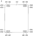
- FIG. 6 is a schematic plan view of the second sealing member in the crystal resonator of the present invention.
- FIG. 7 is a schematic back view of the second sealing member in the crystal resonator of the present invention.
- FIG. 8 is a diagram showing a superposition relationship between the second excitation electrode, one connection terminal, and another connection terminal according to the second embodiment of the crystal resonator of the present invention.
- FIG. 9 is a schematic back view of a second embodiment of the quartz resonator according to the present invention, which is a modified example of the second sealing member showing a superimposed relationship between the second excitation electrode, one connection terminal, and another connection terminal.
- FIG. 10 is a schematic configuration diagram showing each configuration according to the third embodiment of the crystal resonator of the present invention.
- FIG. 11 is a schematic back view of the first sealing member according to the third embodiment of the crystal resonator of the present invention.
- FIG. 12 is a schematic back view of the second sealing member according to the third embodiment of the crystal resonator of the present invention.
- FIG. 13 is a schematic plan view of a function unit in the crystal resonator of the present invention.
- FIG. 14 is a schematic back view of the function part in the crystal resonator of the present invention.
- FIG. 15 is a schematic plan view of a modification of the function unit in the crystal resonator of the present invention.
- FIG. 16 is a schematic plan view of a modification of the function unit in the crystal resonator of the present invention.
- FIG. 17 is a schematic back view of a modified example of the function unit in the crystal resonator of the present invention.
- FIG. 18 is a schematic back view of a modified example of the second sealing member in the crystal resonator of the present invention.
- FIG. 19 is a schematic plan view of a modification of the function unit in the crystal resonator according to the present invention.
- FIG. 20 is a schematic back view of a modified example of the function unit in the crystal resonator of the present invention.
- FIG. 21 is a schematic plan view of a modification of the function unit in the crystal resonator according to the present invention.
- FIG. 22 is a schematic back view of a modification of the function unit in the crystal resonator according to the present invention.
- FIG. 23 is a perspective view showing a wiring state of the third embodiment of the crystal resonator of the present invention.
- FIG. 24 is a schematic configuration diagram showing each configuration according to the first embodiment of the crystal oscillator of the present invention.
- FIG. 25 is a schematic plan view of the first sealing member in the crystal oscillator of the present invention.
- FIG. 26 is a schematic back view of the first sealing member in the crystal oscillator of the present invention.
- FIG. 27 is a schematic plan view of a crystal diaphragm in the crystal oscillator of the present invention.
- FIG. 28 is a schematic back view of the crystal diaphragm in the crystal oscillator of the present invention.
- FIG. 29 is a schematic plan view of a second sealing member in the crystal oscillator of the present invention.
- FIG. 30 is a schematic back view of the second sealing member in the crystal oscillator of the present invention.
- FIG. 31 is a schematic configuration diagram showing each configuration according to the second embodiment of the crystal oscillator of the present invention.
- FIG. 32 is a schematic back view of the second sealing member according to the second embodiment of the crystal oscillator of the present invention.
- FIG. 33 is a schematic plan view of a function unit in the crystal oscillator of the present invention.
- FIG. 34 is a schematic rear view of the function unit in the crystal oscillator of the present invention.
- FIG. 35 is a schematic configuration diagram of a modified example of the function unit in the crystal oscillator of the present invention.
- FIG. 36 is a schematic rear view of a modification of the function unit in the crystal oscillator of the present invention.
- a crystal diaphragm 2 (a piezoelectric diaphragm in the present invention) and a first excitation electrode 221 (see FIG. 4) of the crystal diaphragm 2 are provided.
- a first sealing member 3 that hermetically seals the first excitation electrode 221 formed on one main surface 211 of the crystal diaphragm 2 and the other main surface 212 of the crystal diaphragm 2
- a second sealing member 4 that covers the second excitation electrode 222 (see FIG. 5) and hermetically seals the second excitation electrode 222 formed in a pair with the first excitation electrode 221 is provided.
- the crystal diaphragm 2 and the first sealing member 3 are joined, and the crystal diaphragm 2 and the second sealing member 4 are joined to form a sandwich-structured package 12.
- the vibration part 23 including the first excitation electrode 221 and the second excitation electrode 222 formed on both main surfaces 211 and 212 of the diaphragm 2 is hermetically sealed. As shown in FIG. 1, the internal space 13 is biased to one end side (left side in plan view) of the package 12 in plan view.
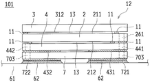
- the crystal resonator 101 has a package size of 1.0 ⁇ 0.8 mm, and is intended to be reduced in size and height.
- the package 12 does not form a castellation and uses the through holes (see the first through hole 261, the second through hole 441, and the third through hole 442) to conduct the electrodes. ing.
- each configuration of the above-described crystal resonator 101 will be described with reference to FIGS.
- each member configured as a single body to which the crystal diaphragm 2, the first sealing member 3, and the second sealing member 4 are not joined will be described.
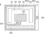
- the quartz diaphragm 2 is made of quartz which is a piezoelectric material, and both main surfaces (one main surface 211 and the other main surface 212) are formed as flat smooth surfaces (mirror finish). Yes.
- a pair of (paired) excitation electrodes (a first excitation electrode 221 and a second excitation electrode 222) are formed on both main surfaces 211 and 212 (one main surface 211 and another main surface 212) of the crystal diaphragm 2. ing.
- the two main surfaces 211 and 212 are formed with two notches 24 (penetrating shape) so as to surround the pair of first excitation electrodes 221 and second excitation electrodes 222 in plan view (see FIGS. 4 and 5).
- the cutout portion 24 includes a concave body 241 in plan view (a plan view body including three plan view rectangles formed by extending two rectangles from both ends of one plan view rectangle in a right angle direction) and a plan view.
- a rectangular body 242 is formed between the concave body 241 in plan view and the rectangular body 242 in plan view.
- the first excitation electrode 221 and the second excitation electrode 222 are connected to external terminals (one connection terminal 431, another connection terminal 432; It is a conduction path 213 in which the extraction electrodes (first extraction electrode 223 and second extraction electrode 224) for extraction to the reference are arranged.
- the first extraction electrode 223 and the second extraction electrode 224 extracted from the pair of first excitation electrode 221 and second excitation electrode 222 are the vibration side first bonding pattern 251 and the vibration side second bonding pattern 252.
- the first sealing member 3 and the second sealing member 4 are bonded to the outside along the vibration part 23 of both main surfaces 211 and 212 so as to surround the vibration part 23.
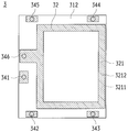
- Each of the vibration side sealing portions 25 is provided. As shown in FIGS. 4 and 5, the vibration-side sealing portion 25 is located biased to the left of the two main surfaces 211 and 212 in plan view.
- a vibration-side first bonding pattern 251 for bonding to the first sealing member 3 is formed on the vibration-side sealing portion 25 of the one main surface 211 of the crystal diaphragm 2, and the first excitation electrode 221 is the vibration-side first electrode 221.
- One connection pattern 251 is connected.
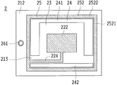
- a vibration side second bonding pattern 252 for bonding to the second sealing member 4 is formed on the vibration side sealing portion 25 of the other main surface 212 of the crystal diaphragm 2, and the second excitation electrode 222 is on the vibration side. It is connected to the second bonding pattern 252.
- the internal space 13 is formed inside (inside) the vibration side first bonding pattern 251 and the vibration side second bonding pattern 252.
- a vibration side first bonding pattern 251 for bonding the first sealing member 3 is formed on one main surface 211 of the crystal diaphragm 2, and the vibration side first bonding pattern 251 is physically disposed on the one main surface 211.
- a vibration-side second bonding pattern 252 for bonding the second sealing member 4 is formed on the other main surface 212 of the crystal diaphragm 2, and the vibration-side second bonding pattern 252 is formed on the other main surface 212.
- the base PVD film 2521 formed by physical vapor deposition on the substrate and the electrode PVD film 2522 formed by physical vapor deposition on the base PVD film 2521 are stacked. That is, the vibration side first bonding pattern 251 and the vibration side second bonding pattern 252 have the same configuration, and a plurality of layers are stacked on the vibration side sealing portion 25 of both main surfaces 211 and 212, A Ti layer (or Cr layer) and an Au layer are formed by vapor deposition from the lowermost layer side.
- the underlying PVD films 2511 and 2521 are made of a single material (Ti (or Cr)), and the electrode PVD films 2512 and 2522 are formed.
- the electrode PVD films 2512 and 2522 are made of a single material (Au) and are thicker than the underlying PVD films 2511 and 2521. Further, the first excitation electrode 221 and the vibration-side first bonding pattern 251 formed on the one main surface 211 of the crystal diaphragm 2 have the same thickness, and the first excitation electrode 221 and the vibration-side first bonding pattern 251 have the same thickness.
- the second excitation electrode 222 and the vibration side second bonding pattern 252 formed on the other major surface 212 of the quartz crystal plate 2 have the same thickness, and the second excitation electrode is made of the same metal.
- the surfaces (main surfaces) of 222 and the vibration side second bonding pattern 252 are made of the same metal.
- the vibration side first bonding pattern 251 and the vibration side second bonding pattern 252 are non-Sn patterns.
- the vibration side first and second bonding patterns 251 and 252 and the vibration side are compared on the same main surface with the same metal and the same thickness. If the metal of the uppermost layer (at least the exposed surface) (electrode PVD films 2512, 2522, etc.) is the same, bonding is performed even if the type and thickness of the base metal (base PVD films 2511, 2521) are different. It is possible.
- the electrode PVD films 2512 and 2522 are the surfaces of the scaly body in plan view.
- the scale-like body here refers to a form in which the activated and microscopic pieces of metal are superposed like a tatami mat and have no gap (or almost no gap) in plan view. Say.
- a first through hole 261 is formed in the crystal diaphragm 2, and the vibration side first joining pattern connected to the first excitation electrode 221 through the first through hole 261. 251 is drawn to the other main surface 212 side.
- the first through-hole 261 is arranged outside the internal space 13 and is located on the other end side in plan view (right side in plan view) of both the main surfaces 211 and 212 as shown in FIG. 261 is not formed inside the internal space 13.
- the inside of the internal space 13 means strictly the inside of the inner peripheral surface of the bonding material 11 without including the bonding material 11.
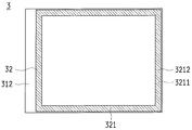
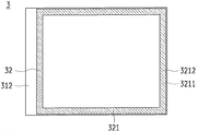
- the first sealing member 3 is made of a material having a bending rigidity (secondary moment of section ⁇ Young's modulus) of 1000 [N ⁇ mm 2 ] or less. Specifically, as shown in FIGS. 2 and 3, the first sealing member 3 is a rectangular parallelepiped substrate formed from a single glass wafer, and the other main surface 312 ( The surface to be bonded to the crystal diaphragm 2 is formed as a flat smooth surface (mirror finish).
- the other main surface 312 of the first sealing member 3 is provided with a sealing-side first sealing portion 32 for joining the crystal diaphragm 2. As shown in FIG. 3, the sealing-side first sealing portion 32 is biased to the left of the other main surface 312 of the first sealing member 3 in plan view.
- a sealing-side first bonding pattern 321 for bonding the crystal diaphragm 2 is formed on the sealing-side first sealing portion 32 of the first sealing member 3.
- the sealing side first bonding pattern 321 has the same width at all positions on the sealing side first sealing portion 32 of the first sealing member 3.
- the sealing-side first bonding pattern 321 is formed by stacking a base PVD film 3211 formed by physical vapor deposition on the first sealing member 3 and a physical vapor deposition on the base PVD film 3211. Electrode PVD film 3212 formed. In this embodiment, Ti (or Cr) is used for the base PVD film 3211 and Au is used for the electrode PVD film 3212. Moreover, the sealing side 1st joining pattern 321 is a non-Sn pattern. Specifically, the sealing side first bonding pattern 321 is configured by laminating a plurality of layers on the sealing side first sealing portion 32 of the other main surface 312, and the Ti layer (or from the lowermost layer side). Cr layer) and Au layer are formed by vapor deposition. In the sealing-side first bonding pattern 321, the electrode PVD film 3212 is the surface of the scaly body in plan view.
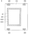
- the second sealing member 4 a material having a bending rigidity (secondary moment of section ⁇ Young's modulus) of 1000 [N ⁇ mm 2 ] or less is used.
- the second sealing member 4 is a rectangular parallelepiped substrate formed from a single glass wafer, and one main surface 411 (quartz crystal vibration) of the second sealing member 4
- the surface joined to the plate 2 is formed as a flat smooth surface (mirror finish).
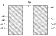
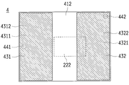
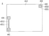
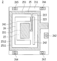
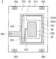
- the main surface 411 of the second sealing member 4 is provided with a sealing-side second sealing portion 42 for joining to the crystal diaphragm 2. As shown in FIG. 6, the sealing-side second sealing portion 42 is located biased to the left of the main surface 411 of the second sealing member 4 in plan view.
- a pair of external terminals (one connection terminal 431, another connection terminal) to be electrically connected to the outside. 432) is formed.
- One connection terminal 431 is electrically connected directly to the first excitation electrode 221 via the vibration side first bonding pattern 251
- the other connection terminal 432 is connected to the second excitation electrode 222 via the vibration side second bonding pattern 252. Electrically connected directly.
- the one connection terminal 431 and the other connection terminal 432 are respectively located at both ends in the longitudinal direction of the other main surface 412 of the second sealing member 4 in the plan view.
- the pair of external terminals are formed on the base PVD films 4311 and 4321 and the base PVD films 4311 and 4321 formed by physical vapor deposition on the other main surface 412.
- the electrode PVD films 4312 and 4322 are formed by physical vapor deposition.
- the thickness of the underlying PVD films 4311 and 4321 of the external terminals is thicker than Further, the one connection terminal 431 and the other connection terminal 432 occupy a region of 1/3 or more of the other main surface 412 of the second sealing member 4.
- a sealing-side second bonding pattern 421 for bonding the crystal diaphragm 2 is formed on the sealing-side second sealing portion 42 of the second sealing member 4.
- the sealing side second bonding pattern 421 has the same width at all positions on the sealing side second sealing portion 42 of the second sealing member 4.
- the sealing-side second bonding pattern 421 is formed by stacking a base PVD film 4211 formed by physical vapor deposition on the second sealing member 4 and a physical vapor deposition on the base PVD film 4211.
- the electrode PVD film 4212 is formed. Note that in this embodiment, Ti (or Cr) is used for the base PVD film 4211 and Au is used for the electrode PVD film 4212.
- the sealing-side second bonding pattern 421 is a non-Sn pattern. Specifically, the sealing-side second bonding pattern 421 is configured by laminating a plurality of layers on the sealing-side second sealing portion 42 of the other main surface 412, and Ti layer (or from the lowermost layer side) Cr layer) and Au layer are formed by vapor deposition. In addition, in the sealing-side second bonding pattern 421, the electrode PVD film 4212 becomes the surface of the scaly body in plan view.
- the second sealing member 4 is formed with two through holes (a second through hole 441 and a third through hole 442) as shown in FIGS.
- the second through-hole 441 and the third through-hole 442 are arranged outside the internal space 13, and the second through-hole 441 has both main surfaces (one main surface 411, another main surface 412 as shown in FIGS. 6 and 7).
- the third through hole 442 is located on the upper left side in plan view, and the second through hole 441 and the third through hole 442 are not formed inside the internal space 13.
- the inside of the internal space 13 means strictly the inside of the inner peripheral surface of the bonding material 11 without including the bonding material 11.
- the vibration side first joint pattern 251 connected to the first excitation electrode 221 of the crystal diaphragm 2 and the one connection terminal 431 are electrically connected via the first through hole 261 and the second through hole 441 of the crystal diaphragm 2. Is done.
- the vibration side second bonding pattern 252 connected to the second excitation electrode 222 of the crystal diaphragm 2 is electrically connected to the other connection terminal 432 through the third through hole 442 and the sealing side second bonding pattern 421.
- the crystal vibrating plate 2 and the first sealing member 3 are connected to the vibration-side first bonding pattern 251 and the bonding member such as an adhesive separately without using a separate bonding material as in the prior art. Diffusion bonding is performed in a state where the sealing-side first bonding pattern 321 is overlapped, and the crystal diaphragm 2 and the second sealing member 4 overlap the vibration-side second bonding pattern 252 and the sealing-side second bonding pattern 421.
- the package 12 having the sandwich structure shown in FIG. 1 is manufactured by diffusion bonding.
- the vibration side first bonding pattern 251 and the sealing side first bonding pattern 321 itself become the bonding material 11 generated after diffusion bonding, and the vibration side second bonding pattern 252 and the sealing side second bonding pattern 421 itself diffuse. It becomes the joining material 11 produced
- diffusion bonding is performed at room temperature.
- the normal temperature here means 5 ° C. to 35 ° C.
- This room-temperature diffusion bonding has the following effects (suppression of gas generation and good bonding), which is a preferred example having a value lower than 183 ° C., which is the melting point of eutectic solder.
- the sealing-side first bonding pattern 321 and the vibration-side first bonding pattern 251 are bonded by diffusion bonding, and the sealing-side second bonding pattern 421 and the vibration-side are bonded.
- the second bonding pattern 252 is bonded.
- the sealing side first bonding pattern 321 and the vibration side first bonding pattern 251 are pressure diffusion bonded, and the sealing side second bonding pattern 421.
- the vibration side second bonding pattern 252 may be pressure diffusion bonded. In this case, it becomes easy to secure the joint location by pressurizing (the joint area can be substantially increased), and the joining by only the diffusion joining can be performed more favorably without using the high temperature heating.
- the first sealing member 3 and the crystal diaphragm 2 have a gap of 1.00 ⁇ m or less, and the second sealing member 4 and the crystal diaphragm 2 are 1 It has a gap of 0.000 ⁇ m or less. That is, the thickness of the bonding material 11 between the first sealing member 3 and the crystal vibrating plate 2 is 1.00 ⁇ m or less, and the bonding material 11 between the second sealing member 4 and the crystal vibrating plate 2 The thickness is 1.00 ⁇ m or less (specifically, 0.15 ⁇ m to 1.00 ⁇ m in the Au—Au bonding of the present embodiment). For comparison, a conventional metal paste sealing material using Sn has a thickness of 5 ⁇ m to 20 ⁇ m.
- the thickness of the bonding pattern in which the sealing-side first bonding pattern 321 and the vibration-side first bonding pattern 251 are diffusion-bonded is such that the sealing-side second bonding pattern 421 and the vibration-side second bonding pattern 252 are diffusion-bonded.
- the thickness of the bonding pattern is the same as the thickness of the external terminal (one connection terminal 431 and the other connection terminal 432) electrically connected to the outside.
- the internal space 13 is located on the left side in plan view.
- the sealing side first bonding pattern 321 formed on the first sealing member 3 and the sealing side second bonding pattern 421 formed on the second sealing member 4 do not overlap in plan view.
- the planar view area in the sealing-side first bonding pattern 321 is wider than the planar view area in the sealing-side second bonding pattern 421.
- the planar view area in the sealing-side first bonding pattern 321 is wider than the planar view area in the sealing-side second bonding pattern 421, but the present invention is not limited to this.
- the planar view region in the stop-side second joining pattern 421 may be wider than the planar view region in the sealing-side first joining pattern 321.
- the planar view region in the sealing side first bonding pattern 321 is in the sealing side second bonding pattern 421. Since the wiring pattern is wider than the planar view area, the wiring pattern can be easily routed (conducting a conduction path), and the wiring pattern routing area (conduction ensuring area) can be increased.
- the sealing side first bonding pattern 321 formed on the first sealing member 3 and the first 2 is wide.
- the sandwiched crystal resonator 101 can eliminate the generation of gas, and can be further reduced in height and size.
- the sealing-side first bonding pattern 321 and the vibration-side first bonding are used. Since the pattern 251 is diffusion bonded and the sealing side second bonding pattern 421 and the vibration side second bonding pattern 252 are diffusion bonded, it is not necessary to use a metal paste sealing material separately, which contributes to cost reduction. be able to.
- the underlying PVD films 2511 and 2521 are formed by PVD methods such as vacuum deposition, sputtering, ion plating, MBE, and laser ablation (for example, film forming methods for patterning in processing such as photolithography).
- the package of the piezoelectric vibration device is currently being downsized. For this reason, while preventing a problem such as a short circuit due to interference of patterns (electrode patterns) and terminals (electrode pads) having different polarities, Au- It is difficult to print a metal paste sealing material such as Sn.
- a metal paste sealing material such as Sn.
- sealing side first and second joining patterns 321 and 421 and the vibration side first and second joining patterns 251 and 252 are used, it is possible to easily cause problems such as short-circuiting due to interference of patterns or terminals having different polarities. Pattern formation can be performed while preventing.
- a metal paste sealing material such as Au—Sn is separately used, but in the case of joining using this metal paste sealing material, it is always heated at a high temperature for fusion joining. And gas is generated during heat-melting. A technique for eliminating this gas has not been developed at present, and gas intrusion into the internal space is unavoidable during heat-melt bonding.
- the sealing side first bonding pattern 321 and the vibration side first bonding pattern 251 are diffusion bonded, and the sealing side second bonding pattern 421 and the vibration side second bonding pattern are combined. Therefore, the generation of gas can be suppressed, and the deterioration of vibration characteristics due to the presence of gas in the internal space 13 can be prevented.
- a temperature higher than room temperature such as 220 ° C. may be applied, but applying a high temperature (for example, 280 ° C. or more) as in the bonding using the metal paste sealing material is not possible. Absent.
- the sealing-side first and second bonding patterns 321 and 421 and the vibration-side first and second bonding patterns 251 and 252 are respectively formed of the underlying PVD films 2511, 2521, 3211 and 4211 and the electrodes. Since it has a laminated structure with PVD films 2512, 2522, 3212, and 4212, it is possible to reduce the width of patterns and terminals to make them thinner, and as a result, hinders the miniaturization of the package caused by pattern routing. Can be eliminated. Specifically, according to the present embodiment, patterns and terminals that cannot be realized with a piezoelectric vibration device using bonding with a metal paste sealing material such as Au—Sn can be thinned.
- the sealing side first bonding pattern 321 and the vibration side first bonding pattern 251 are diffusion bonded, and the sealing side second bonding pattern 421 and the vibration side second bonding pattern 252 are formed. Since diffusion bonding is performed, high-temperature heat-melt bonding is not performed. For this reason, when the crystal unit 101 is bonded to an external member such as an external circuit using solder or the like, it is not remelted at the bonding portion, and the bonding state does not change in a reflow or product use environment. .
- sealing side first bonding pattern 321 and the vibration side first bonding pattern 251 are bonded at room temperature
- the sealing side second bonding pattern 421 and the vibration side second bonding pattern 252 are bonded at room temperature. This is suitable for suppressing generation of gas and preventing deterioration of vibration characteristics due to the presence of gas in the internal space 13. Moreover, it does not remelt at the joining location, and the joining state does not change.
- sealing-side first bonding pattern 321 and the vibration-side first bonding pattern 251 are diffusion-bonded at a temperature not lower than room temperature and lower than 230 ° C.
- sealing-side second bonding pattern 421 and the vibration-side second bonding pattern 252 are Since diffusion bonding is performed at a temperature not lower than room temperature and lower than 230 ° C., it is possible to improve the bonding while suppressing the generation of gas.
- first excitation electrode 221 and the vibration-side first bonding pattern 251 formed on the one main surface 211 of the crystal diaphragm 2 have the same thickness, and the first excitation electrode 221 and the vibration-side first bonding pattern 251 have the same thickness.
- the second excitation electrode 222 and the vibration side second bonding pattern 252 formed on the other major surface 212 of the quartz crystal plate 2 have the same thickness, and the second excitation electrode is made of the same metal. Since the surface (main surface) of 222 and the vibration side second bonding pattern 252 are made of the same metal, it is possible to form the metal film of the first excitation electrode 221 and the vibration side first bonding pattern 251 only once.
- the metal film of the second excitation electrode 222 and the vibration side second bonding pattern 252 it is possible to form the metal film of the second excitation electrode 222 and the vibration side second bonding pattern 252 only once.
- the metal film of the first excitation electrode 221 and the vibration side first bonding pattern 251 can be made the same, and the metal film of the second excitation electrode 222 and the vibration side second bonding pattern 252 can be made the same. .
- the underlying PVD films 2511 and 2521 are made of a single material
- the electrode PVD films 2512 and 2522 are made of a single material
- the underlying PVD film 2511 is made.
- 2521 is thicker than the electrode PVD films 2512 and 2522, it is possible to prevent a single material constituting the underlying PVD films 2511 and 2521 from diffusing into the electrode PVD films 2512 and 2522.
- each base PVD film 2511, 2521, 3211, 4211 of the vibration side first bonding pattern 251, the vibration side second bonding pattern 252, the sealing side first bonding pattern 321, and the sealing side second bonding pattern 421 Since the base PVD films 4311 and 4321 of the external terminals (one connection terminal 431 and the other connection terminal 432) are thick, the first sealing member 3, the second sealing member 4, and the crystal vibrating plate 2 are joined. Since the external terminals (one connection terminal 431 and the other connection terminal 432) are electrically connected to the outside (for example, solder mounting) while being stabilized, the base metal (the one connection terminal 431 and the other connection terminal 432) is the base.
- the PVD films 4311 and 4321 can be effectively used to electrically connect to the outside.
- the vibration side first bonding pattern 251, the vibration side second bonding pattern 252, the sealing side first bonding pattern 321, the sealing side second bonding pattern 421, and external terminals one connection terminal 431 and other connection terminal 432.
- external terminals one connection terminal 431, other connection terminal 432 (for example, Solder mounting etc. cannot be performed.
- the vibration side first bonding pattern 251, the vibration side second bonding pattern 252, the sealing side first bonding pattern 321, and the sealing side second bonding pattern 421 are used. It is difficult to oxidize the surfaces of the first and second vibration-side first bonding patterns 251, vibration-side second bonding patterns 252, sealing-side first bonding patterns 321, and sealing-side second bonding patterns 421. Special pre-processing is not required. As a result, the manufacturing cost can be suppressed. Regarding the pre-manufacturing process here, according to this configuration, the atmosphere environment does not have to be an ultra-high vacuum, for example.
- the vibration side first bonding pattern 251, the vibration side second bonding pattern 252, the sealing side first bonding pattern 321, and the sealing side second bonding pattern 421 are non-Sn patterns, and therefore do not require high-temperature heating during bonding. There is no problem (remelting) due to high-temperature heat bonding.
- the underlying PVD films 2511 and 2521 are formed by PVD methods such as vacuum deposition, sputtering, ion plating, MBE, and laser ablation (for example, film forming methods for patterning in processing such as photolithography). , 3211, 4211 and the electrode PVD films 2512, 2522, 3212, 4212 are formed, which can contribute to cost reduction.
- the pattern can be thinned, and a defect such as a short circuit due to interference of patterns or terminals having different polarities does not occur.
- first sealing member 3 and the second sealing member 4 are made of an insulating (brittle) material having a bending rigidity (secondary moment of section ⁇ Young's modulus) of 1000 [N ⁇ mm 2 ] or less. It becomes possible to satisfy the deformation amount necessary for joining. Therefore, for example, the bending rigidity within the above range can be obtained without forming the electrode surfaces such as the first excitation electrode 221 and the second excitation electrode 222 to have a surface roughness (Ra) of 1 nm or less necessary for normal bonding. By doing so, diffusion bonding can be performed.
- a surface roughness
- sealing side first bonding pattern 321 and the vibration side first bonding pattern 251 are pressure diffusion bonded without using a separate bonding dedicated material, and the sealing side second bonding pattern 421 and the vibration side second bonding pattern are bonded. 252 and pressure diffusion bonding, it is possible to contribute to downsizing, in particular, low profile, and there is a limit to the low profile when using a dedicated joint material. It can be turned upside down.
- the thickness of the bonding pattern in which the sealing-side first bonding pattern 321 and the vibration-side first bonding pattern 251 are diffusion-bonded is such that the sealing-side second bonding pattern 421 and the vibration-side second bonding pattern 252 are diffusion-bonded. Since the thickness of the bonding pattern is the same as that of the external terminals (one connection terminal 431 and the other connection terminal 432) electrically connected to the outside, the thickness of the underlying PVD films 2511, 2521, 3211 and 4211 is different at the time of diffusion bonding. Diffusion can be reliably prevented, and the bonding strength of each of the underlying PVD films 2511, 2521, 3211, and 4211 to the first sealing member 3, the second sealing member 4, and the crystal diaphragm 2 can be increased.
- connection terminal 431 and the other connection terminal 432 are electrically connected to the outside (for example, by solder mounting), so that the underlying PVD films 4311 and 4321 are electrically connected to the outside. It can be used effectively.
- the through holes (second through hole 441 and third through hole 442) arranged outside the internal space 13 are formed in the second sealing member 4, the through holes (second through hole 441, first through hole 441) are formed.
- the through holes (second through hole 441 and third through hole 442) are arranged inward of the internal space 13 without the influence of the three through holes 442) reaching the internal space 13. Airtight defects caused by the second through hole 441 and the third through hole 442) can be avoided.
- the through hole when the through hole is arranged in the internal space, it is necessary to ensure the airtightness of the internal space, and a process of filling the through hole in the internal space with a metal or the like is required.
- the vibration side first bonding pattern 251 and the vibration are vibrated.
- the wiring pattern can be routed in the same process as the pattern formation of the second side bonding pattern 252, the sealing side first bonding pattern 321, and the sealing side second bonding pattern 421, and the manufacturing cost can be reduced.
- sealing side first bonding pattern 321 and the sealing side second bonding pattern 421 do not overlap in plan view, stray capacitance is generated by the sealing side first bonding pattern and the sealing side second bonding pattern 421. Can be prevented.
- the width of the bonding pattern between the vibration side first bonding pattern 251 and the vibration side second bonding pattern 252 becomes narrower.
- the first sealing member 3 and the second sealing member 4 are looser in dimensional constraints than the vibration part 23, the bonding pattern between the sealing side first bonding pattern 321 and the sealing side second bonding pattern 421. As a result, the degree of freedom in alignment accuracy during bonding can be increased.
- the height of the package of the crystal unit 101 does not vary.
- the Sn bonding material in which the gap between the sealing member (first sealing member 3 and second sealing member 4 in the present embodiment) and the crystal diaphragm 2 is larger than 1 ⁇ m.
- the metal paste sealing material is patterned (vibration side first bonding pattern 251, vibration side second bonding pattern 252, sealing side first bonding pattern 321, sealing side second. The height at the time of forming on the bonding pattern 421) varies.
- this problem becomes conspicuous as the height is lowered. Therefore, in this embodiment, since the upper limit of the gap is set to 1.00 ⁇ m, the three members of the first sealing member 3, the second sealing member 4, and the crystal diaphragm 2 are kept in parallel. In this state, they can be laminated and joined, and this embodiment can cope with a reduction in height.
- quartz is used for the piezoelectric diaphragm, but the present invention is not limited to this, and other materials may be used as long as they are piezoelectric materials, such as lithium niobate, lithium tantalate, etc. It may be.
- the bonding material 11 may be composed of, for example, Ni and Au. .
- the vibration side first bonding pattern 251, the vibration side second bonding pattern 252, the sealing side first bonding pattern 321, and the sealing side second bonding pattern 421 include Ti (or Cr) and Au.
- Cu Cu simple substance or Cu alloy
- it contributes to stress relaxation at the time of manufacturing (when joining, impact caused by external force such as pressurization) or during use (when impact caused by external force such as dropping, solder mounting, etc.) be able to. That is, the mechanical strength is improved by including Cu in the vibration side first bonding pattern 251, the vibration side second bonding pattern 252, the sealing side first bonding pattern 321, and the sealing side second bonding pattern 421.
- Cr when Cr is used for the underlying PVD films 2511, 2521, 3211, and 4211, Cr diffuses into the electrode PVD films 2512, 2522, 3212, and 4212, and Cu is diffused into the underlying PVD films 2511, 2521, 3211, and 4211. It can suppress by including. As a result, even if the layer using Cr is thickened, it is possible to suppress the diffusion of Cr into the electrode PVD films 2512, 2522, 3212, and 4212, and the layer using Cr can be made thick. Variation can be suppressed. Actually, even if the Cr layer is 0.2 ⁇ m, the diffusion of Cr into the electrode PVD films 2512, 2522, 3212, and 4212 can be suppressed.
- the second sealing member 4 is a rectangular parallelepiped substrate formed from a single glass wafer, but is not limited to this, and the two sealing members 4 are formed from two rectangular parallelepipeds formed from a glass wafer.
- the sealing-side second bonding pattern 421, the third through-hole 442, and the other connection terminals 432 are formed in one rectangular parallelepiped substrate, and hermetically sealed by this substrate, and the other rectangular parallelepiped substrate is formed.
- the second through hole 441 and the one connection terminal 431 are formed. According to this configuration, the pair of external terminals (one connection terminal 431 and the other connection terminal 432) can be completely separated, and a short circuit can be prevented. Further, when two rectangular parallelepiped second sealing members 4 are formed of a metal material instead of a glass wafer, there is no need to form third through holes 442, and the number of through holes is reduced, contributing to downsizing. it can.
- the first extraction electrode 223 and the second extraction electrode 224 as shown in FIGS. 1 to 7 are formed.
- the present invention is not limited to this, and the first extraction electrode 223 and the second extraction electrode 224 are not limited thereto.
- Cr is used for the uppermost layer at an arbitrary position of the two extraction electrodes 224, and there is a gap between the first extraction electrode 223, the second extraction electrode 224 and the vibration side first bonding pattern 251 and the vibration side second bonding pattern 252. There may be.
- the gap is preferably provided on the vibration side sealing portion 25.
- the first extraction electrode 223, the second extraction electrode 224, the vibration side first bonding pattern 251, the vibration side second bonding pattern 252, and the like, before performing heat-melt bonding in the manufacturing process Will not be electrically connected.
- various inspections for only the excitation electrodes first excitation electrode 221 and second excitation electrode 222 can be performed in the inspection process for performing vibration inspection, and the degree of freedom of vibration inspection is increased.
- the vibration side first bonding pattern 251 is connected to the first excitation electrode 221, and the vibration side second bonding pattern 252 is connected to the second excitation electrode 222.
- the second excitation electrode 222 overlaps with the other connection terminal 432 and does not overlap with the one connection terminal 431.
- the internal space 13 of the quartz crystal resonator 101 manufactured here is located on the left side in plan view.
- the second sealing member 4 is formed with through holes (second through hole 441 and third through hole 442) arranged outside the internal space 13, and through holes are formed inside the internal space 13. (Second through hole 441 and third through hole 442) are not formed.
- the excitation electrode and the external terminal are superposed (in the present embodiment, the second excitation electrode 222 and the other connection terminal 432). Even if it exists, generation
- the vibration side first bonding pattern 251 is connected to the first excitation electrode 221
- the vibration side second bonding pattern 252 is connected to the second excitation electrode 222
- the second excitation electrode 222 is connected to the other connection terminal 432. Since the second excitation electrode 222 and the other connection terminal 432 having the same polarity as the second excitation electrode 222 do not overlap, no stray capacitance is generated. Further, the quartz resonator 101 having the sandwich structure can be reduced in size while suppressing the stray capacitance from being generated by the second excitation electrode 222 being superimposed on the one connection terminal 431 having a different polarity with respect to the second excitation electrode 222. Can be achieved.
- the through-hole (2nd through-hole 441, 3rd through-hole 442) distribute
- the second through hole 441 and the third through hole 442 are compared with the configuration in which the second through hole 441 and the third through hole 442 are arranged inward of the internal space 13 without the influence of the 442 affecting the internal space 13. Airtight defects caused by can be avoided.
- the through hole when the through hole is arranged in the internal space, it is necessary to ensure the airtightness of the internal space, and a process of filling the through hole in the internal space with a metal or the like is required.
- the vibration side first bonding pattern 251 and the vibration are vibrated.
- the wiring pattern can be routed in the same process as the pattern formation of the second side bonding pattern 252, the sealing side first bonding pattern 321, and the sealing side second bonding pattern 421, and the manufacturing cost can be reduced.
- a through hole (second through hole) is formed on the other end side in plan view (right side in plan view).
- the hole 441) and the electrode pattern can be easily formed, and the formation of the electrode pattern that affects the first excitation electrode 221 and the second excitation electrode 222 disposed in the internal space 13 can be facilitated.
- the arrangement of through holes (second through hole 441 and third through hole 442) that affect the hermetic sealing of the internal space 13 can be facilitated.
- first sealing member 3 is formed with a sealing-side first bonding pattern 321 having the same width at all positions, and the second sealing member 4 is sealed with the same width at all positions.
- the side second bonding pattern 421 is formed, and through holes (second through holes 441 and third through holes 442) arranged outside the internal space 13 are formed in the second sealing member 4. It is possible to suppress the flow of the bonding material 11 to the wider pattern width due to the difference in the widths of the patterns. As a result, the first sealing member 3 and the second sealing member 4 are bonded to the crystal diaphragm 2. The state can be stabilized.
- the second excitation electrode 222 is configured to overlap the other connection terminal 432 and not to overlap the one connection terminal 431, but is not limited thereto.
- the second excitation electrode 222 shown in FIG. 9 may be superposed on the one connection terminal 431 and the other connection terminal 432.
- the vibration-side first bonding pattern 251 is directly connected to the first excitation electrode 221, and the vibration-side second bonding pattern 252 is directly connected to the second excitation electrode 222.
- the second excitation electrode 222 is superimposed on the one connection terminal 431 and the other connection terminal 432, and the second excitation electrode 222 is one more than the portion superimposed on the other connection terminal 432. A portion overlapping the connection terminal 431 is small.
- stray capacitance is generated even when the excitation electrode and the external terminal are superposed in the sandwiched crystal resonator 101. Can be suppressed.
- the vibration side first bonding pattern 251 is connected to the first excitation electrode 221
- the vibration side second bonding pattern 252 is connected to the second excitation electrode 222
- the second excitation electrode 222 overlaps with the one connection terminal 431 and the other connection terminal 432
- the second excitation electrode 222 has a smaller portion overlapping with the one connection terminal 431 than the portion overlapped with the other connection terminal 432.
- No stray capacitance is generated even if 222 and the other connection terminal 432 having the same polarity as the second excitation electrode 222 are superimposed, and the second excitation electrode 222 is not connected to the second excitation electrode 222.
- the vibration side first bonding pattern 251 is connected to the first excitation electrode 221
- the vibration side second bonding pattern 252 is connected to the second excitation electrode 222
- the second excitation electrode 222 is Since the portion of the one connection terminal 431 that overlaps with the second excitation electrode 222 is small in the one connection terminal 431 and the other connection terminal 432, what is the other connection terminal 432 that has the same polarity as the second excitation electrode 222? Even if they are superimposed, no stray capacitance is generated, and the sandwiched crystal resonator 101 is reduced in size by suppressing the amount of stray capacitance generated by the second excitation electrode 222 and one connection terminal 431 being superimposed. Can be planned.
- the crystal resonator 101 is electrically connected to the circuit board 61 and serves as a basis for oscillation in the circuit board 61.
- a piezoelectric diaphragm) and a first excitation electrode 221 (see FIG. 4) of the quartz diaphragm 2, and a first excitation electrode 221 formed on one main surface 211 of the quartz diaphragm 2 is hermetically sealed.
- the sealing member 3 and the other main surface 212 of the crystal diaphragm 2 cover the second excitation electrode 222 (see FIG. 5) of the crystal diaphragm 2 and are formed in pairs with the first excitation electrode 221.
- a second sealing member 4 that hermetically seals the two excitation electrodes 222 is provided.
- the crystal diaphragm 2 and the first sealing member 3 are joined, and the crystal diaphragm 2 and the second sealing member 4 are joined to form a sandwich-structured package 12.
- the 1st sealing member 3 and the 2nd sealing member 4 are joined via the crystal diaphragm 2, and the internal space 13 of the package 12 is formed,
- the vibration part 23 including the first excitation electrode 221 and the second excitation electrode 222 formed on both main surfaces 211 and 212 of the diaphragm 2 is hermetically sealed.
- the internal space 13 is located biased toward one end side (left side in plan view) of the package 12 in plan view.
- This sandwich structure package 12 is provided with a function unit 7 to form a function expansion type crystal unit 101.
- the crystal resonator 101 has a package size of 1.0 ⁇ 0.8 mm, and is intended to be reduced in size and height.
- the package 12 does not form a castellation and uses the through holes (see the first through hole 261, the second through hole 441, and the third through hole 442) to conduct the electrodes. ing.
- each configuration of the crystal unit 101 will be described with reference to FIGS.
- each member configured as a single unit to which the constituent members of the crystal unit 101 are not joined will be described.
- the quartz diaphragm 2 is made of a quartz substrate, which is a piezoelectric material, and its main surfaces (one main surface 211 and the other main surface 212) are formed as flat smooth surfaces (mirror finish). Has been.
- a pair of (paired) excitation electrodes (a first excitation electrode 221 and a second excitation electrode 222) are formed on both main surfaces 211 and 212 (one main surface 211 and the other main surface 212) of the crystal diaphragm 2.
- the two main surfaces 211 and 212 are formed with two cutout portions 24 (penetrating shape) so as to surround the pair of first excitation electrode 221 and second excitation electrode 222 in plan view (see FIGS. 4 and 5).
- the cutout portion 24 includes a concave body 241 in plan view (a plan view body including three plan view rectangles formed by extending two rectangles from both ends of one plan view rectangle in a right angle direction) and a plan view.
- a rectangular body 242 is formed between the concave body 241 in plan view and the rectangular body 242 in plan view.
- the first excitation electrode 221 and the second excitation electrode 222 are connected to the external terminals (first external electrode terminals 721 of the function unit 7).
- the second external electrode terminal 722; see below) is a conduction path 213 in which lead electrodes (first lead electrode 223 and second lead electrode 224) for lead are provided.
- the first extraction electrode 223 and the second extraction electrode 224 extracted from the pair of the first excitation electrode 221 and the second excitation electrode 222 respectively include the vibration side first bonding pattern 251 and the vibration side second bonding pattern 252.
- connection terminals one connection terminal 431, the other connection terminal 432 formed on the second sealing member 4 are electrically connected.
- the connection terminals (one connection terminal 431 and other connection terminal 432) are electrically connected to external terminals (first external electrode terminal 721 and second external electrode terminal 722) formed in the function unit 7.
- the first sealing member 3 and the second sealing member 4 are bonded to the outside along the vibrating portion 23 of both main surfaces 211 and 212 so as to surround the vibrating portion 23.
- Each of the vibration side sealing portions 25 is provided. As shown in FIGS. 4 and 5, the vibration-side sealing portion 25 is located on the left side of the two main surfaces 211 and 212 in plan view.
- a vibration-side first bonding pattern 251 for bonding to the first sealing member 3 is formed on the vibration-side sealing portion 25 of the one main surface 211 of the crystal diaphragm 2, and the first excitation electrode 221 is the vibration-side first electrode 221.
- One connection pattern 251 is connected.
- a vibration side second bonding pattern 252 for bonding to the second sealing member 4 is formed on the vibration side sealing portion 25 of the other main surface 212 of the crystal diaphragm 2, and the second excitation electrode 222 is on the vibration side. It is connected to the second bonding pattern 252.
- the internal space 13 is formed inside (inside) the vibration side first bonding pattern 251 and the vibration side second bonding pattern 252.
- a vibration side first bonding pattern 251 for bonding the first sealing member 3 is formed on one main surface 211 of the crystal diaphragm 2, and the vibration side first bonding pattern 251 is physically disposed on the one main surface 211.
- a vibration-side second bonding pattern 252 for bonding the second sealing member 4 is formed on the other main surface 212 of the crystal diaphragm 2, and the vibration-side second bonding pattern 252 is formed on the other main surface 212.
- the base PVD film 2521 formed by physical vapor deposition on the substrate and the electrode PVD film 2522 formed by physical vapor deposition on the base PVD film 2521 are stacked.
- the film formed by physical vapor deposition unlike electroplating or electroless plating of wet plating, there is no surface roughness and airtightness can be secured, and there is no surface roughness and diffusion is achieved. Bonding can be performed.
- the vibration-side first bonding pattern 251 and the vibration-side second bonding pattern 252 have the same configuration, and a plurality of layers are stacked on the vibration-side sealing portion 25 of both main surfaces 211 and 212. Then, a Ti layer (or Cr layer) and an Au layer are formed by vapor deposition from the lowermost layer side.
- the underlying PVD films 2511 and 2521 are made of a single material (Ti (or Cr)), and the electrode PVD films 2512 and 2522 are formed.
- the electrode PVD films 2512 and 2522 are made of a single material (Au) and are thicker than the underlying PVD films 2511 and 2521.
- first excitation electrode 221 and the vibration-side first bonding pattern 251 formed on the one main surface 211 of the crystal diaphragm 2 have the same thickness, and the first excitation electrode 221 and the vibration-side first bonding pattern 251 have the same thickness.
- the second excitation electrode 222 and the vibration side second bonding pattern 252 formed on the other major surface 212 of the quartz crystal plate 2 have the same thickness, and the second excitation electrode is made of the same metal.
- the surfaces (main surfaces) of 222 and the vibration side second bonding pattern 252 are made of the same metal.
- the vibration side first bonding pattern 251 and the vibration side second bonding pattern 252 are non-Sn patterns.
- the vibration side first and second bonding patterns 251 and 252 are compared with the vibration side (the first excitation electrode 221 and the second excitation electrode 222) with the same metal and the same thickness on the same main surface. If the metal of the uppermost layer (at least the exposed surface) (electrode PVD films 2512, 2522, etc.) is the same, bonding is performed even if the type and thickness of the base metal (base PVD films 2511, 2521) are different. It is possible.
- the electrode PVD films 2512 and 2522 are the surfaces of the scaly body in a plan view.
- the scale-like body here refers to a form in which the activated and microscopic pieces of metal are superposed like a tatami mat and have no gap (or almost no gap) in plan view. Say.
- a first through hole 261 is formed in the crystal diaphragm 2, and the vibration side first joining pattern connected to the first excitation electrode 221 through the first through hole 261. 251 is drawn to the other main surface 212 side.
- the first through hole 261 is disposed outside the internal space 13, and is located on the other end side (right side in plan view) of both the main surfaces 211 and 212 as shown in FIG. 261 is not formed inside the internal space 13.
- the inside of the internal space 13 means strictly the inside of the inner peripheral surface of the bonding material 11 without including the bonding material 11.
- the first sealing member 3 is made of a material having a bending rigidity (secondary moment of section ⁇ Young's modulus) of 1000 [N ⁇ mm 2 ] or less. Specifically, as shown in FIGS. 2 and 11, the first sealing member 3 is a rectangular parallelepiped substrate formed from one glass wafer, and the other main surface 312 of the first sealing member 3 ( The surface to be bonded to the crystal diaphragm 2 is formed as a flat smooth surface (mirror finish).
- the other main surface 312 of the first sealing member 3 is provided with a sealing-side first sealing portion 32 for joining to the crystal diaphragm 2. As shown in FIG. 11, the first sealing portion 32 on the sealing side is biased to the left of the other main surface 312 of the first sealing member 3 in plan view.
- a sealing-side first bonding pattern 321 for bonding to the crystal diaphragm 2 is formed on the sealing-side first sealing portion 32 of the first sealing member 3.
- the sealing side first bonding pattern 321 has the same width at all positions on the sealing side first sealing portion 32 of the first sealing member 3.
- the sealing-side first bonding pattern 321 is formed by stacking a base PVD film 3211 formed by physical vapor deposition on the first sealing member 3 and a physical vapor deposition on the base PVD film 3211. Electrode PVD film 3212 formed. In this embodiment, Ti (or Cr) is used for the base PVD film 3211 and Au is used for the electrode PVD film 3212. Moreover, the sealing side 1st joining pattern 321 is a non-Sn pattern. Specifically, the sealing side first bonding pattern 321 is configured by laminating a plurality of layers on the sealing side first sealing portion 32 of the other main surface 312, and the Ti layer (or from the lowermost layer side). Cr layer) and Au layer are formed by vapor deposition. In the sealing-side first bonding pattern 321, the electrode PVD film 3212 is the surface of the scaly body in plan view.
- the second sealing member 4 a material having a bending rigidity (secondary moment of section ⁇ Young's modulus) of 1000 [N ⁇ mm 2 ] or less is used.
- the second sealing member 4 is a rectangular parallelepiped substrate formed from a single glass wafer, and one main surface 411 (quartz crystal vibration) of the second sealing member 4
- the surface joined to the plate 2 is formed as a flat smooth surface (mirror finish).
- the main surface 411 of the second sealing member 4 is provided with a sealing-side second sealing portion 42 for joining to the crystal diaphragm 2. As shown in FIG. 6, the sealing-side second sealing portion 42 is located biased to the left of the main surface 411 of the second sealing member 4 in plan view.
- connection terminals one of which can be electrically connected to the function unit (see FIG. 13)
- a connection terminal 431 and another connection terminal 432 are formed.
- the function unit 7 is formed with external terminals (first external electrode terminal 721 and second external electrode terminal 722) that directly match the circuit board 61 as described below.
- connection terminal 431 is electrically connected directly to the first excitation electrode 221 via the vibration side first bonding pattern 251, and the other connection terminal 432 is connected to the second excitation electrode 222 via the vibration side second bonding pattern 252. Electrically connected directly.
- the one connection terminal 431 is disposed at a part of one end side in the longitudinal direction of the other main surface 412 of the second sealing member 4, and the other connection terminal 432 is disposed at a corner portion on the other end side. Has been placed.
- the function unit 7 is an inductance unit 74 described later, as shown in FIG. 18, the one connection terminal 431 is arranged along the short side in the longitudinal direction in plan view.
- connection terminals are formed on the base PVD films 4311 and 4321 and the base PVD films 4311 and 4321 formed by physical vapor deposition on the other main surface 412.
- the electrode PVD films 4312 and 4322 are formed by physical vapor deposition.
- the underlying PVD films 4311 and 4321 of the connection terminals are the vibration side first bonding pattern 251, the vibration side second bonding pattern 252, and the sealing side first bonding pattern 321.
- the underlying PVD films 2511, 2521, 3211, and 4211 of the sealing-side second bonding pattern 421 have the same thickness.
- a sealing-side second bonding pattern 421 for bonding the crystal diaphragm 2 is formed on the sealing-side second sealing portion 42 of the second sealing member 4.
- the sealing side second bonding pattern 421 has the same width at all positions on the sealing side second sealing portion 42 of the second sealing member 4.
- the sealing-side second bonding pattern 421 is formed by stacking a base PVD film 4211 formed by physical vapor deposition on the second sealing member 4 and a physical vapor deposition on the base PVD film 4211.
- the electrode PVD film 4212 is formed. Note that in this embodiment, Ti (or Cr) is used for the base PVD film 4211 and Au is used for the electrode PVD film 4212.
- the sealing-side second bonding pattern 421 is a non-Sn pattern. Specifically, the sealing-side second bonding pattern 421 is configured by laminating a plurality of layers on the sealing-side second sealing portion 42 of the other main surface 412, and Ti layer (or from the lowermost layer side) Cr layer) and Au layer are formed by vapor deposition. In addition, in the sealing-side second bonding pattern 421, the electrode PVD film 4212 becomes the surface of the scaly body in plan view.
- the second sealing member 4 has two through holes (a second through hole 441 and a third through hole 442).
- the second through-hole 441 and the third through-hole 442 are disposed outside the internal space 13, and the second through-hole 441 has both main surfaces (one main surface 411 and another main surface 412 as shown in FIGS.
- the third through hole 442 is located on the upper left side in the plan view, and the second through hole 441 and the third through hole 442 are not formed inside the internal space 13.
- the inside of the internal space 13 means strictly the inside of the inner peripheral surface of the bonding material 11 without including the bonding material 11.
- the vibration side first joint pattern 251 connected to the first excitation electrode 221 of the crystal diaphragm 2 and the one connection terminal 431 are electrically connected via the first through hole 261 and the second through hole 441 of the crystal diaphragm 2. Is done.
- the vibration side second bonding pattern 252 connected to the second excitation electrode 222 of the crystal diaphragm 2 is electrically connected to the other connection terminal 432 through the third through hole 442 and the sealing side second bonding pattern 421.
- the crystal diaphragm 2 and the first sealing member 3 are connected to the vibration-side first bonding pattern 251 and the bonding member such as a separate adhesive as in the prior art. Diffusion bonding is performed in a state where the sealing-side first bonding pattern 321 is overlapped, and the crystal diaphragm 2 and the second sealing member 4 overlap the vibration-side second bonding pattern 252 and the sealing-side second bonding pattern 421.
- the sandwiched package 12 is manufactured by diffusion bonding.
- the sandwich-structured package 12 is in a form that can be distributed.
- the vibration side first bonding pattern 251 and the sealing side first bonding pattern 321 itself become the bonding material 11 generated after diffusion bonding, and the vibration side second bonding pattern 252 and the sealing side second bonding pattern 421 itself diffuse. It becomes the joining material 11 produced
- diffusion bonding is performed at room temperature.
- the normal temperature here means 5 ° C. to 35 ° C.
- This room-temperature diffusion bonding has the following effects (suppression of gas generation and good bonding), which is a preferred example having a value lower than 183 ° C., which is the melting point of eutectic solder.
- the sealing-side first bonding pattern 321 and the vibration-side first bonding pattern 251 are bonded by diffusion bonding, and the sealing-side second bonding pattern 421 and the vibration-side are bonded.
- the second bonding pattern 252 is bonded.
- the sealing side first bonding pattern 321 and the vibration side first bonding pattern 251 are pressure diffusion bonded, and the sealing side second bonding pattern 421.
- the vibration side second bonding pattern 252 may be pressure diffusion bonded. In this case, it becomes easy to secure the joint location by pressurizing (the joint area can be substantially increased), and the joining by only the diffusion joining can be performed more favorably without using the high temperature heating.
- the first sealing member 3 and the crystal diaphragm 2 have a gap of 1.00 ⁇ m or less, and the second sealing member 4 and the crystal diaphragm 2 are 1 It has a gap of 0.000 ⁇ m or less. That is, the thickness of the bonding material 11 between the first sealing member 3 and the crystal vibrating plate 2 is 1.00 ⁇ m or less, and the bonding material 11 between the second sealing member 4 and the crystal vibrating plate 2 The thickness is 1.00 ⁇ m or less (specifically, 0.15 ⁇ m to 1.00 ⁇ m in the Au—Au bonding of the present embodiment). For comparison, a conventional metal paste sealing material using Sn has a thickness of 5 ⁇ m to 20 ⁇ m.
- the internal space 13 is biased to the left in plan view.
- the sealing side 1st joining pattern 321 (refer FIG. 11) formed in the 1st sealing member 3 and the sealing side 2nd joining pattern 421 (refer FIG. 6) formed in the 2nd sealing member 4 are used. Does not overlap in plan view.
- the planar view area in the sealing-side first bonding pattern 321 is wider than the planar view area in the sealing-side second bonding pattern 421.
- the planar view area in the sealing-side first bonding pattern 321 is wider than the planar view area in the sealing-side second bonding pattern 421, but the present invention is not limited to this.
- the planar view region in the stop-side second joining pattern 421 may be wider than the planar view region in the sealing-side first joining pattern 321.
- the planar view region in the sealing side first bonding pattern 321 is in the sealing side second bonding pattern 421.
- the wiring pattern can be easily routed (conducting a conduction path), and more wiring patterns can be provided (conduction ensuring area).
- the sealing side first bonding pattern 321 formed on the first sealing member 3 and the first 2 is wide.
- the package 12 manufactured as described above is provided with a function unit 7 (see FIG. 13) in which an external terminal directly mated with the circuit board 61 is formed, so that crystal vibrations for various uses are provided.
- the child 101 (function expansion type crystal resonator 101) is obtained.
- the second sealing member 4 and the function unit 7 are connected to a connection terminal (one connection terminal 431, another connection terminal 432) and an internal electrode terminal (first internal electrode terminal 711, second internal electrode terminal 712).
- the function expansion type crystal resonator 101 is manufactured by diffusion bonding in a state where the layers are superposed. Then, as shown in FIG.
- the function expansion type crystal resonator 101 is directly coupled to the circuit board 61 using the fluid conductive bonding material 62 and is electrically connected thereto.
- the second sealing member 4 and the function portion 7 have a gap of 1.00 ⁇ m or less (specifically, the Au of the present embodiment). -0.15 ⁇ m to 1.00 ⁇ m for Au bonding)
- a conventional metal paste sealing material using Sn has a thickness of 5 ⁇ m to 20 ⁇ m.
- one main surface 701 of the function unit 7 is a connection terminal (one connection terminal 431, other connection) formed on the second sealing member 4.
- Internal electrode terminals first internal electrode terminal 711, second internal electrode terminal 712) that are directly connected to the terminal 432) and are electrically connected to the second sealing member 4, and internals that are electrically connected to elements to be described later Electrode terminals (third internal electrode terminal 713, fourth internal electrode terminal 714) are formed.
- the first internal electrode terminal 711 is electrically connected directly to the one connection terminal 431, and the second internal electrode terminal 712 is electrically connected directly to the other connection terminal 432.
- first internal electrode terminal 711, second internal electrode terminal 712, third internal electrode terminal 713, and fourth internal electrode terminal 714) are formed by physical vapor deposition on one main surface 701.
- the underlying PVD films 7111, 7121, 7131, 7141 of the internal electrode terminals (first internal electrode terminal 711, second internal electrode terminal 712, third internal electrode terminal 713, fourth internal electrode terminal 714)
- Side first bonding pattern 251, vibration side second bonding pattern 252, sealing side first bonding pattern 321, sealing side second bonding pattern 421, and connection bases (one connection terminal 431, other connection terminal 432)
- the films 2511, 2521, 3211, 4211, 4311, and 4321 have the same thickness.
- a first external electrode terminal 721, a second external electrode terminal 722, a third external electrode terminal 723, and a fourth external electrode terminal 724) are formed.
- the external terminals are internal electrode terminals (first internal electrode terminal 711, second internal electrode terminal 712).
- the third internal electrode terminal 713 and the fourth internal electrode terminal 714) are electrically connected directly via the function part through hole 703.
- first external electrode terminal 721, second external electrode terminal 722, third external electrode terminal 723, and fourth external electrode terminal 724) were formed by physical vapor deposition on the other main surface 702.
- the substrate PVD films 7211, 7221, 7231, and 7241, and electrode PVD films 7212, 7222, 7232, and 7242 formed by physical vapor deposition on the underlying PVD films 7211, 7221, 7231, and 7241 are formed.
- the vibration side first bonding pattern 251, the vibration side second bonding pattern 252, the sealing side first bonding pattern 321, the sealing side second bonding pattern 421, and connection terminals one connection terminal 431, another connection terminal 432).
- External terminals (first external electrode terminal 721, second external electrode terminal 722, third external electrode terminal 723, fourth external) with respect to the thickness of each of the underlying PVD films 2511, 2521, 3211, 4211, 4311, 4321
- the base PVD films 7211, 7221, 7231, 7241 of the electrode terminals 724) are thick.
- the thickness of the bonding pattern in which the sealing-side first bonding pattern 321 and the vibration-side first bonding pattern 251 in the package 12 are diffusion-bonded is as follows: the sealing-side second bonding pattern 421 and the vibration-side second bonding pattern
- the external terminals (first external electrode terminal 721, second external electrode terminal 722, third external electrode terminal 723, fourth external electrode) having the same thickness as the bonding pattern formed by diffusion bonding with 252 and electrically connected to the outside Unlike the thickness of the terminal 724), the external terminals (the first external electrode terminal 721, the second external electrode terminal 722, the third external electrode terminal 723, and the fourth external electrode terminal 724) are thicker than the other patterns.
- the function unit 7 shown in FIGS. 13 and 14 is provided with a temperature measuring element unit 73.
- the temperature measuring element unit 73 here is a thermistor, a diode, or the like.
- the temperature measuring element unit 73 is electrically connected via a third internal electrode terminal 713 and a fourth internal electrode terminal 714.
- the conventional small crystal resonator 101 cannot be provided with the temperature measuring element.
- the temperature measuring element is not provided. Can be provided.
- the function unit 7 shown in FIGS. 13 and 14 is provided with the temperature measuring element unit 73, but the function unit 7 is limited to the one provided with the temperature measuring element unit 73. Instead, the form of the function unit 7 is not limited as long as it has an arbitrary function and forms an external terminal.
- the function unit 7 as shown in FIGS. 15 to 17, the external terminals (first external electrode terminal 721, second external electrode terminal 722, third external electrode terminal 723, and fourth external electrode terminal 724) are The internal electrode terminals (first internal electrode terminal 711, second internal electrode terminal 712, third internal electrode terminal 713, and fourth internal electrode terminal 714) are electrically connected directly.
- the function unit 7 shown in FIG. 15 is provided with a heater unit 77 having a heater element instead of the temperature measuring element unit 73 of FIG.
- the heater portion 77 has a shape that meanders between the internal electrode terminals.
- an impact absorbing epoxy substrate is used for the function unit 7.
- it can be used as a piezoelectric vibration device mounted on a vehicle, and the epoxy substrate absorbs the impact even under severe conditions in the impact environment, and the vibration portion 23 is not affected by the impact.
- 16 and 17 may be provided with a temperature measuring element portion 73 shown in FIG. 13, a heater portion 77 shown in FIG. 15, and an inductance portion 74 shown in FIGS.
- the function part 7 is provided with an inductance part 74 of an L element.
- the inductance portion 74 is obtained by winding a thin film conductive pattern around a substrate using an L element through hole 741. According to the function unit 7, it is possible to increase the capacity that decreases as the crystal unit 101 becomes smaller.
- the function unit 7 When the function unit 7 is the inductance unit 74, the function unit 7 is placed under the function unit 7 as shown in FIGS. It is preferable to provide the function unit 7 that avoids contact between the inductance unit 74 and the circuit board 61. That is, it is preferable to stack the function units 7 (see FIG. 23).
- the function unit 7 shown in FIGS. 20 and 21 is provided with the inductance unit 74, but the function unit 7 is not limited to the one provided with the inductance unit 74, and is arbitrary. If the function is provided and an external terminal is formed, the form of the function unit 7 is not limited.
- the inductance portion 74 Crystal unit 101 having an L element
- crystal unit 101 having a temperature measuring unit 73 thermoometer unit
- crystal unit 101 having a heater unit 77 heater element
- in-vehicle X'tal It is possible to cope with various uses such as the quartz crystal resonator 101 of FIG.
- the fluid conductive bonding material 62 (Pb-free solder, conductive adhesive, or the like) cannot be directly bonded to the connection terminals (one connection terminal 431, the other connection terminal 432).
- This is a thin PVD film 4311, 4321 of a connection terminal (one connection terminal 431, another connection terminal 432) formed by physical vapor deposition and is suitable for diffusion bonding, but high temperature heating is essential. This is because it is not suitable for the required joining (solder joining, etc.). Therefore, in the present embodiment, the connection terminals (one connection terminal 431 and the other connection terminal 432) cannot be directly combined with the circuit board 61 serving as an external member via the fluid conductive bonding material 62.
- connection terminal one connection terminal 431, the other connection terminal 432. Therefore, according to the present embodiment, the connection terminal (one connection terminal 431, The other connection terminal 432) is not eaten by the fluid conductive bonding material 62. Therefore, the connection terminals (the one connection terminal 431 and the other connection terminal 432) may be formed thin without considering the amount of the connection terminal (the one connection terminal 431 and the other connection terminal 432) eroded by the fluid conductive bonding material 62. As a result, the crystal resonator 101 can be reduced in height.
- the sealing side first bonding pattern 321 and the vibration side first bonding pattern 251 are diffusion bonded, and the sealing side second bonding pattern 421 and the vibration side second bonding pattern 252 are formed.
- connection terminals one connection terminal 431 and another connection terminal 432) for diffusion bonding to the function unit 7 are formed on the other main surface 412 that does not face the crystal diaphragm 2 in the second sealing member 4. Therefore, the crystal diaphragm 2, the first sealing member 3, and the second excitation electrode 222 are not joined by the high temperature heating, and the connection terminals (one connection terminal 431 and the other connection terminal 432) are deteriorated by the high temperature heating at the time of joining. Does not cause.
- the function unit 7 is diffusion bonded to the second sealing member 4, and external terminals (a first external electrode terminal 721, a second external electrode terminal 722, a third external electrode terminal 723, and a fourth external electrode terminal are connected to the function unit 7. 724) is formed, the function unit 7 can be interposed when the crystal diaphragm 2 is mounted on the circuit board 61. As a result, the thermal expansion of the material of the circuit board 61 and the constituent material of the crystal resonator 101 is achieved. It is possible to prevent a malfunction (for example, cracking of a joint solder crack) from occurring due to the coefficient difference, and the reliability of the crystal unit 101 is greatly improved.
- a malfunction for example, cracking of a joint solder crack
- the height of the package of the crystal unit 101 does not vary.
- the gap between the sealing members (the first sealing member 3 and the second sealing member 4 in the present embodiment), the crystal diaphragm 2 and the function unit 7 is greater than 1 ⁇ m.
- the metal paste sealing material is patterned (vibration side first bonding pattern 251, vibration side second bonding pattern 252, sealing side first bonding pattern 321, sealing The height at the time of forming on the stop side second joining pattern 421) varies.
- the three laminated members are joined in a state where the parallelism cannot be maintained. In particular, this problem becomes conspicuous as the height is lowered.
- the upper limit of the gap is set to 1.00 ⁇ m
- the first sealing member 3, the second sealing member 4, and the crystal vibrating plate 2 are three pieces. (Furthermore, according to the function expansion type crystal resonator 101, the first sealing member 3, the second sealing member 4, the crystal diaphragm 2, and the function portion 7 or more members) are parallel. In this state, it can be laminated and joined, and this embodiment can cope with a reduction in height.
- the function part 7 is joined to the second sealing member 4, but the present invention is not limited to this, and the function part 7 may be joined to the first sealing member 3. .
- quartz is used for the piezoelectric diaphragm, but the present invention is not limited to this, and other materials may be used as long as they are piezoelectric materials, such as lithium niobate, lithium tantalate, etc. It may be.
- the bonding material 11 may be composed of, for example, Ni and Au. .
- the conductive film is formed on the inner wall surface of the through hole in all the through holes.
- the present invention is not limited to this, and the through hole may be filled with a conductive material.
- the vibration side first bonding pattern 251, the vibration side second bonding pattern 252, the sealing side first bonding pattern 321, and the sealing side second bonding pattern 421 include Ti (or Cr) and Au.
- Cu Cu simple substance or Cu alloy
- it contributes to stress relaxation at the time of manufacturing (when joining, impact caused by external force such as pressurization) or during use (when impact caused by external force such as dropping, solder mounting, etc.) be able to. That is, the mechanical strength is improved by including Cu in the vibration side first bonding pattern 251, the vibration side second bonding pattern 252, the sealing side first bonding pattern 321, and the sealing side second bonding pattern 421.
- the second sealing member 4 is a rectangular parallelepiped substrate formed from a single glass wafer, but is not limited to this, and the two sealing members 4 are formed from two rectangular parallelepipeds formed from a glass wafer.
- the sealing-side second bonding pattern 421, the third through-hole 442, and the other connection terminals 432 are formed in one rectangular parallelepiped substrate, and hermetically sealed by this substrate, and the other rectangular parallelepiped substrate is formed.
- the second through hole 441 and the one connection terminal 431 are formed. According to this configuration, the pair of connection terminals (one connection terminal 431 and the other connection terminal 432) can be completely separated, and a short circuit can be prevented. Further, when two rectangular parallelepiped second sealing members 4 are formed of a metal material instead of a glass wafer, there is no need to form third through holes 442, and the number of through holes is reduced, contributing to downsizing. it can.
- the first extraction electrode 223 and the second extraction electrode 224 as shown in FIGS. 2, 4 to 6, and 10 to 12 are formed.
- Cr is used for the uppermost layer at an arbitrary position of the first extraction electrode 223 and the second extraction electrode 224, and the first extraction electrode 223, the second extraction electrode 224, the vibration side first bonding pattern 251 and the vibration side second bonding pattern 252 are used. There may be a gap between them. In particular, the gap is preferably provided on the vibration side sealing portion 25.
- the first extraction electrode 223, the second extraction electrode 224, the vibration side first bonding pattern 251, and the vibration side second bonding pattern 252 before the heat-melt bonding in the manufacturing process are performed. Will not be electrically connected.
- various inspections for only the excitation electrodes can be performed in the inspection process for performing vibration inspection, and the degree of freedom of vibration inspection is increased.
- a glass epoxy substrate may be used for the function section 7 shown in FIGS.
- the electrode formed on the glass-epoxy substrate is difficult to perform diffusion bonding described in the previous embodiment, and therefore the electrode is formed by Au bumps.
- the soldering between the function unit 7 (glass epoxy substrate) and the circuit board 61 becomes possible. Since the mounting solder used for joining has a small difference in thermal expansion coefficient from the glass epoxy substrate, it is possible to suppress the occurrence of solder cracks during mounting. Therefore, since it can be set as a highly reliable piezoelectric vibration device, it can be used for in-vehicle mounting.
- the glass epoxy substrate may be provided with a temperature measuring element unit 73 shown in FIG. 13, a heater unit 77 shown in FIG. 15, and an inductance unit 74 shown in FIGS.
- the present invention may be a crystal oscillator (see FIG. 24) as described below.
- a crystal oscillator see FIG. 24
- two embodiments in which the present invention is applied to a crystal oscillator as a piezoelectric vibration device that performs piezoelectric vibration will be described.
- the same reference numerals are assigned to the same components as those of the crystal unit 101 described above.
- the operational effects produced by the common configuration are the same as those of the crystal resonator 101 shown in FIG.
- the crystal diaphragm 2 pieoelectric diaphragm in the present invention
- the first excitation electrode 221 see FIG. 27
- the first sealing member 3 that hermetically seals the first excitation electrode 221 formed on the one main surface 211 of the crystal diaphragm 2, and the second main surface 212 of the crystal diaphragm 2 has the first sealing member 3.
- a second sealing member 4 that covers the second excitation electrode 222 (see FIG. 28) and hermetically seals the second excitation electrode 222 formed in a pair with the first excitation electrode 221 is mounted on the first sealing member.
- Electronic component elements (IC5 in the present embodiment) other than the piezoelectric vibration element thus formed are provided.
- the vibration part 23 including the first excitation electrode 221 and the second excitation electrode 222 formed on both main surfaces 211 and 212 of the diaphragm 2 is hermetically sealed. Note that the internal space 13 is located biased toward one end side (left side in plan view) of the package 12 as shown in FIG.
- the crystal oscillator 102 has a package size of 1.2 ⁇ 1.0 mm and is small and low-profile.
- the package 12 uses the through holes (the fourth through hole 262 to the eighteenth through hole 446) to conduct the electrodes without forming a castellation.
- each configuration of the crystal oscillator 102 will be described with reference to FIGS.
- each member configured as a single body to which the crystal diaphragm 2, the first sealing member 3, and the second sealing member 4 are not joined will be described.
- the quartz diaphragm 2 is made of quartz, which is a piezoelectric material, and both principal surfaces (one principal surface 211, the other principal surface 212) are formed as flat smooth surfaces (mirror finish). Yes.
- a pair of (paired) excitation electrodes (a first excitation electrode 221 and a second excitation electrode 222) are formed on both main surfaces 211 and 212 (one main surface 211 and another main surface 212) of the crystal diaphragm 2. ing.
- the two main surfaces 211 and 212 are formed with two notches 24 (penetrating shape) so as to surround the pair of first excitation electrodes 221 and second excitation electrodes 222, thereby constituting the vibration part 23.
- the cutout 24 includes a concave body 241 in plan view (three rectangles in plan view, each of which is formed by extending two rectangles from both ends of a rectangle in plan view in a direction perpendicular to the longitudinal direction of the rectangle).
- the first excitation electrode 221 and the second excitation electrode 222 are external terminals (see below) between the concave shape body 241 and the rectangular shape 242 in plan view. It is a conduction path 213 in which the extraction electrodes (first extraction electrode 223 and second extraction electrode 224) for drawing out are arranged. Regarding the electrode pattern, the first extraction electrode 223 and the second extraction electrode 224 extracted from the pair of first excitation electrode 221 and second excitation electrode 222 are the vibration side first bonding pattern 251 and the vibration side second bonding pattern 252. Is electrically connected to the electrode pattern 33 formed on the first sealing member 3.
- the first sealing member 3 and the second sealing member 4 are bonded to the outside along the vibration part 23 of both main surfaces 211 and 212 so as to surround the vibration part 23.
- Each of the vibration side sealing portions 25 is provided. As shown in FIGS. 27 and 28, the vibration-side sealing portion 25 is biased to the left of the two main surfaces 211 and 212 in plan view.
- a vibration-side first bonding pattern 251 for bonding the first sealing member 3 is formed on the vibration-side sealing portion 25 of the main surface 211 of the crystal diaphragm 2, and the first excitation electrode 221 is on the vibration side. It is connected to the first bonding pattern 251.
- the vibration-side first bonding pattern 251 includes a base PVD film 2511 formed by physical vapor deposition on one main surface 211 and an electrode PVD formed by physical vapor deposition on the base PVD film 2511 and stacked.
- a vibration side second bonding pattern 252 for bonding the second sealing member 4 is formed on the vibration side sealing portion 25 of the other main surface 212 of the crystal diaphragm 2, and the second excitation electrode 222 vibrates.
- the vibration-side second bonding pattern 252 includes a base PVD film 2521 formed by physical vapor deposition on the other main surface 212 and an electrode PVD formed by physical vapor deposition on the base PVD film 2521 and stacked. A film 2522.
- the internal space 13 is formed inside (inside) the vibration side first bonding pattern 251 and the vibration side second bonding pattern 252.
- the vibration-side first bonding pattern 251 and the vibration-side second bonding pattern 252 have the same configuration, and a plurality of layers are stacked on the vibration-side sealing portions 25 of both main surfaces 211 and 212.
- a Ti layer (or Cr layer) and an Au layer are vapor-deposited from the lower layer side.
- the underlying PVD films 2511 and 2521 are made of a single material (Ti (or Cr)), and the electrode PVD films 2512 and 2522 are formed.
- the electrode PVD films 2512 and 2522 are made of a single material (Au) and are thicker than the underlying PVD films 2511 and 2521.
- first excitation electrode 221 and the vibration-side first bonding pattern 251 formed on the one main surface 211 of the crystal diaphragm 2 have the same thickness, and the first excitation electrode 221 and the vibration-side first bonding pattern 251 have the same thickness.
- the second excitation electrode 222 and the vibration side second bonding pattern 252 formed on the other major surface 212 of the quartz crystal plate 2 have the same thickness, and the second excitation electrode is made of the same metal.
- the surfaces (main surfaces) of 222 and the vibration side second bonding pattern 252 are made of the same metal.
- the vibration side first bonding pattern 251 and the vibration side second bonding pattern 252 are non-Sn patterns.
- the vibration side first and second bonding patterns 251 and 252 and the vibration side are compared on the same main surface with the same metal and the same thickness. If the metal of the uppermost layer (at least the exposed surface) (electrode PVD films 2512, 2522, etc.) is the same, bonding is performed even if the type and thickness of the base metal (base PVD films 2511, 2521) are different. It is possible.
- the electrode PVD films 2512 and 2522 are the surfaces of the scaly body in plan view.
- the scale-like body here refers to a form in which the activated and microscopic pieces of metal are superposed like a tatami mat and have no gap (or almost no gap) in plan view. Say.
- the crystal diaphragm 2 has through holes (fourth through hole 262, fifth through hole 263, sixth through hole 264, seventh through hole 265, and eighth through hole 266. ) And the vibration side second bonding pattern 252 connected to the second excitation electrode 222 is drawn out to the one main surface 211 side through the fourth through hole 262.
- the fifth through hole 263 is connected to the tenth through hole 342 of the first sealing member 3 and the fifteenth through hole 443 of the second sealing member 4, and conducts the IC 5 to the first connection terminal 433. It is a conduction path for.
- the sixth through hole 264 is connected to the eleventh through hole 343 of the first sealing member 3 and the sixteenth through hole 444 of the second sealing member, and conducts the IC 5 to the second connection terminal 434. It is a conduction path.
- the seventh through hole 265 is connected to the twelfth through hole 344 of the first sealing member 3 and the seventeenth through hole 445 of the second sealing member, and conducts the IC 5 to the third connection terminal 435. It is a conduction path.
- the eighth through hole 266 is connected to the thirteenth through hole 345 of the first sealing member 3 and the eighteenth through hole 446 of the second sealing member, and conducts the IC 5 to the fourth connection terminal 436. It is a conduction path.
- the fourth through hole 262, the fifth through hole 263, the sixth through hole 264, the seventh through hole 265, and the eighth through hole 266 are formed outside the internal space 13. Further, the fourth through hole 262, the fifth through hole 263, the sixth through hole 264, the seventh through hole 265, and the eighth through hole 266 are not formed inside the internal space 13.
- the inside of the internal space 13 means strictly the inside of the inner peripheral surface of the bonding material 11 without including the bonding material 11.
- the first sealing member 3 is made of a material having a bending rigidity (secondary moment of section ⁇ Young's modulus) of 1000 [N ⁇ mm 2 ] or less. Specifically, as shown in FIGS. 25 and 26, the first sealing member 3 is a rectangular parallelepiped substrate formed from one glass wafer, and the other main surface 312 ( The surface to be bonded to the quartz crystal plate 2 and one main surface 311 (surface on which the IC 5 is mounted) are formed as a flat smooth surface (mirror finish).
- the other main surface 312 of the first sealing member 3 is provided with a sealing-side first sealing portion 32 for joining to the crystal diaphragm 2. As shown in FIG. 26, the first sealing portion 32 on the sealing side is located on the left side in plan view of the other main surface 312 of the first sealing member 3.
- a sealing-side first bonding pattern 321 for bonding to the crystal diaphragm 2 is formed on the sealing-side first sealing portion 32 of the first sealing member 3.
- the sealing side first bonding pattern 321 has the same width at all positions on the sealing side first sealing portion 32 of the first sealing member 3.
- the sealing-side first bonding pattern 321 is formed by stacking a base PVD film 3211 formed by physical vapor deposition on the first sealing member 3 and a physical vapor deposition on the base PVD film 3211. Electrode PVD film 3212 formed. In this embodiment, Ti (or Cr) is used for the base PVD film 3211 and Au is used for the electrode PVD film 3212. Moreover, the sealing side 1st joining pattern 321 is a non-Sn pattern. Specifically, the sealing side first bonding pattern 321 is configured by laminating a plurality of layers on the sealing side first sealing portion 32 of the other main surface 312, and the Ti layer (or from the lowermost layer side). Cr layer) and Au layer are formed by vapor deposition. In the sealing-side first bonding pattern 321, the electrode PVD film 3212 is the surface of the scaly body in plan view.
- six electrode patterns 33 including a mounting pad for mounting the IC 5 that is an oscillation circuit element are formed. These six electrode patterns 33 are individually guided to the ninth through hole 341, the tenth through hole 342, the eleventh through hole 343, the twelfth through hole 344, the thirteenth through hole 345, and the fourteenth through hole 346, respectively. Yes.
- the tenth through hole 342, the eleventh through hole 343, the twelfth through hole 344, and the thirteenth through hole 345 are through holes for conducting the oscillator, and the ninth through hole 341 (the second excitation electrode 222).
- Through-holes for the conduction of the first excitation electrode 221) are through-holes for conducting the crystal diaphragm 2. As shown in FIG.
- the second sealing member 4 a material having a bending rigidity (secondary moment of section ⁇ Young's modulus) of 1000 [N ⁇ mm 2 ] or less is used.
- the second sealing member 4 is a rectangular parallelepiped substrate formed from a single glass wafer, and one main surface 411 ( The surface to be bonded to the crystal diaphragm 2 is formed as a flat smooth surface (mirror finish).
- the main surface 411 of the second sealing member 4 is provided with a sealing-side second sealing portion 42 for joining to the crystal diaphragm 2. As shown in FIG. 29, the second sealing portion 42 on the sealing side is biased to the left of the main surface 411 of the second sealing member 4 in the plan view.
- first connection terminals 433, 2nd electrically connected to the outside.
- a connection terminal 434, a third connection terminal 435, and a fourth connection terminal 436) are provided.
- the first connection terminal 433, the second connection terminal 434, the third connection terminal 435, and the fourth connection terminal 436 are located at four corners, respectively.
- These external terminals are underlying PVD films 4331 formed by physical vapor deposition on the other main surface 412.
- the thickness of the underlying PVD films 4331, 4341, 4351, and 4361 of the external terminals is thick.
- a sealing-side second bonding pattern 421 for bonding to the crystal diaphragm 2 is formed on the sealing-side second sealing portion 42 of the second sealing member 4.
- the sealing side second bonding pattern 421 has the same width at all positions on the sealing side second sealing portion 42 of the second sealing member 4.
- the sealing-side second bonding pattern 421 is formed by stacking a base PVD film 4211 formed by physical vapor deposition on the second sealing member 4 and a physical vapor deposition on the base PVD film 4211.
- the electrode PVD film 4212 is formed. Note that in this embodiment, Ti (or Cr) is used for the base PVD film 4211 and Au is used for the electrode PVD film 4212.
- the sealing-side second bonding pattern 421 is a non-Sn pattern. Specifically, the sealing-side second bonding pattern 421 is configured by laminating a plurality of layers on the sealing-side second sealing portion 42 of the one main surface 411, and the Ti layer (or from the lowermost layer side) Cr layer) and Au layer are formed by vapor deposition. In addition, in the sealing-side second bonding pattern 421, the electrode PVD film 4212 becomes the surface of the scaly body in plan view.
- the second sealing member 4 has four through holes (a fifteenth through hole 443, a sixteenth through hole 444, a seventeenth through hole 445, and an eighteenth through hole 446). ) Is formed.
- the fifteenth through-hole 443, the sixteenth through-hole 444, the seventeenth through-hole 445, and the eighteenth through-hole 446 are arranged outside the internal space 13, and the fifteenth through-hole 443, the sixteenth through-hole 444, and the seventeenth through-hole 446 are arranged.
- the through hole 445 and the eighteenth through hole 446 are not formed inside the internal space 13.
- the crystal vibrating plate 2 and the first sealing member 3 are connected to the vibration-side first bonding pattern 251 and the sealing-side first without using a separate bonding dedicated material as in the prior art. Diffusion bonding is performed in a state in which the bonding pattern 321 is overlaid, and diffusion bonding is performed in a state in which the crystal diaphragm 2 and the second sealing member 4 are overlaid on the vibration side second bonding pattern 252 and the sealing side second bonding pattern 421.
- the sandwich-structured package 12 shown in FIG. 24 is manufactured.
- the vibration side first bonding pattern 251 and the sealing side first bonding pattern 321 itself become the bonding material 11 generated after diffusion bonding, and the vibration side second bonding pattern 252 and the sealing side second bonding pattern 421 itself diffuse. It becomes the joining material 11 produced
- diffusion bonding is performed at room temperature (5 ° C. to 35 ° C.).
- the present invention is not limited to room temperature diffusion bonding, and may be diffusion bonded at a temperature not lower than room temperature and lower than 230 ° C. In particular, when diffusion bonding is performed at a temperature of 200 ° C.
- the melting point of the Pb-free solder is lower than 230 ° C., and the Au recrystallization temperature (200 ° C.) or higher is reached.
- the stable region can be stabilized.
- the recrystallization temperature can be made higher than Au.
- the sealing-side first bonding pattern 321 and the vibration-side first bonding pattern 251 are bonded by diffusion bonding, and the sealing-side second bonding pattern 421 and the vibration-side are bonded.
- the second bonding pattern 252 is bonded.
- the sealing side first bonding pattern 321 and the vibration side first bonding pattern 251 are pressure diffusion bonded, and the sealing side second bonding pattern 421.
- the vibration side second bonding pattern 252 may be pressure diffusion bonded. In this case, it becomes easy to secure the joint location by pressurizing (the joint area can be substantially increased), and the joining by only the diffusion joining can be performed more favorably without using the high temperature heating.
- the first sealing member 3 and the crystal diaphragm 2 have a gap of 1.00 ⁇ m or less, and the second sealing member 4 and the crystal diaphragm 2 are 1 It has a gap of 0.000 ⁇ m or less. That is, the thickness of the bonding material 11 between the first sealing member 3 and the crystal vibrating plate 2 is 1.00 ⁇ m or less, and the bonding material 11 between the second sealing member 4 and the crystal vibrating plate 2 The thickness is 1.00 ⁇ m or less (specifically, 0.15 ⁇ m to 1.00 ⁇ m in the Au—Au bonding of the present embodiment). For comparison, a conventional metal paste sealing material using Sn has a thickness of 5 ⁇ m to 20 ⁇ m.
- the thickness of the bonding pattern in which the sealing-side first bonding pattern 321 and the vibration-side first bonding pattern 251 are diffusion-bonded is such that the sealing-side second bonding pattern 421 and the vibration-side second bonding pattern 252 are diffusion-bonded.
- the thickness of the bonding pattern is the same as the thickness of the external terminal (first connection terminal 433, second connection terminal 434, third connection terminal 435, fourth connection terminal 436) electrically connected to the outside.
- the internal space 13 is located on the left side in plan view.
- the sealing side first bonding pattern 321 formed on the first sealing member 3 and the sealing side second bonding pattern 421 formed on the second sealing member 4 do not overlap in plan view.
- the planar view area in the sealing-side first bonding pattern 321 is wider than the planar view area in the sealing-side second bonding pattern 421.
- the planar view area in the sealing-side first bonding pattern 321 is wider than the planar view area in the sealing-side second bonding pattern 421, but the present invention is not limited to this.
- the planar view region in the stop-side second joining pattern 421 may be wider than the planar view region in the sealing-side first joining pattern 321.
- the external terminals the first connection terminal 433, the second connection terminal 434, the third connection terminal 435, and the fourth connection terminal 436) are formed on the second sealing member, the sealing side first bonding pattern
- the planar view area in 321 is wider than the planar view area in the sealing-side second bonding pattern 421. Therefore, the wiring pattern can be easily routed (conducting a conduction path), and the wiring pattern routing area (conduction ensuring area) can be increased.
- the sealing side first bonding pattern 321 formed on the first sealing member 3 and the first 2 The width
- a space for providing the IC 5 need not be provided in the crystal diaphragm 2, and the package can be reduced in height. Further, it is possible to cope with an arbitrary oscillation condition simply by changing the pattern for the IC 5 formed on the one main surface of the first sealing member 3. Further, marking can be performed on the back surface of the IC 5, and special marking is not required even when a transparent material is used for the first sealing member 3.
- the first sealing member 3 and the crystal diaphragm 2 are provided with a recess and the oscillation circuit element is always mounted in the recess, the outer shape of the piezoelectric oscillation device is always more than the oscillation circuit element. Was also getting bigger.
- the IC 5 is provided on the one main surface 311 and the other main surface 312 is joined to the one main surface 211 of the crystal diaphragm 2.
- the size and the size of the crystal oscillator 102 can be made the same, which is advantageous for miniaturization and low profile.
- the generation of gas can be eliminated and the height and size can be further reduced, as in the case of the crystal resonator 101 having the sandwich structure. Further, the same configuration and effect as those of the quartz crystal resonator 101 having the sandwich structure are the same.
- the sealing side first bonding pattern 321 formed on the first sealing member 3 and the first 2 is wide.
- the external terminals are the four terminals of the first connection terminal 433, the second connection terminal 434, the third connection terminal 435, and the fourth connection terminal 436.
- the present invention is not limited, and the present invention can be applied to any external terminal having six terminals or eight terminals.
- the crystal oscillator 102 is electrically connected to the circuit board 61 and serves as a basis for oscillation in the circuit board 61. As shown in FIG. Piezoelectric diaphragm) and the first excitation electrode 221 (see FIG.
- a second sealing member 4 that hermetically seals the excitation electrode 222 and an electronic component element (IC5 in the present embodiment) other than the piezoelectric vibration element mounted on the first sealing member are provided.
- the crystal diaphragm 2 and the first sealing member 3 are joined, and the crystal diaphragm 2 and the second sealing member 4 are joined to form a sandwich structure package 12.
- the 1st sealing member 3 and the 2nd sealing member 4 are joined via the crystal diaphragm 2, and the internal space 13 of the package 12 is formed,
- the vibration part 23 including the first excitation electrode 221 and the second excitation electrode 222 formed on both main surfaces 211 and 212 of the diaphragm 2 is hermetically sealed.
- the internal space 13 is biased to one end side (left side in plan view) of the package 12 in plan view.
- the function unit 7 is provided in the package 12 having the sandwich structure, so that the function expansion type crystal oscillator 102 is obtained.
- the crystal oscillator 102 has a package size of 1.2 ⁇ 1.0 mm and is small and low-profile.
- the package 12 uses the through holes (the fourth through hole 262 to the eighteenth through hole 446) to conduct the electrodes without forming a castellation.
- each configuration of the crystal oscillator 102 will be described with reference to FIGS. 25 to 29, 31, and 32.
- FIG. Here, each member constituted as a single unit to which the constituent members of the crystal oscillator 102 are not joined will be described.
- the crystal diaphragm 2 is made of a quartz crystal substrate, which is a piezoelectric material, and both main surfaces (one main surface 211 and the other main surface 212) are formed as flat smooth surfaces (mirror surface processing). Has been.
- a pair of (paired) excitation electrodes (a first excitation electrode 221 and a second excitation electrode 222) are formed on both main surfaces 211 and 212 (one main surface 211 and the other main surface 212) of the crystal diaphragm 2.
- the two main surfaces 211 and 212 are formed with two notches 24 (penetrating shape) so as to surround the pair of first excitation electrode 221 and second excitation electrode 222, thereby constituting the vibration part 23.
- the cutout 24 includes a concave body 241 in plan view (three rectangles in plan view, each of which is formed by extending two rectangles from both ends of one rectangle in plan view in a direction perpendicular to the longitudinal direction of the rectangle).
- a conduction path 213 is provided in which extraction electrodes (first extraction electrode 223 and second extraction electrode 224) for extraction to the terminal are arranged.
- the first extraction electrode 223 and the second extraction electrode 224 extracted from the pair of the first excitation electrode 221 and the second excitation electrode 222 respectively include the vibration side first bonding pattern 251 and the vibration side second bonding pattern 252. Is electrically connected to the electrode pattern 33 formed on the first sealing member 3.
- the first sealing member 3 and the second sealing member 4 are bonded to the outside along the vibrating portion 23 of both main surfaces 211 and 212 so as to surround the vibrating portion 23.
- Each of the vibration side sealing portions 25 is provided. As shown in FIGS. 27 and 28, the vibration-side sealing portion 25 is biased to the left of the two main surfaces 211 and 212 in plan view.
- a vibration-side first bonding pattern 251 for bonding to the first sealing member 3 is formed on the vibration-side sealing portion 25 of the one main surface 211 of the crystal diaphragm 2, and the first excitation electrode 221 is the vibration-side first electrode 221.
- One connection pattern 251 is connected.
- the vibration-side first bonding pattern 251 includes a base PVD film 2511 formed by physical vapor deposition on one main surface 211 and an electrode PVD formed by physical vapor deposition on the base PVD film 2511 and stacked.
- a vibration side second bonding pattern 252 for bonding to the second sealing member 4 is formed on the vibration side sealing portion 25 of the other main surface 212 of the crystal diaphragm 2, and the second excitation electrode 222 is on the vibration side.
- the vibration-side second bonding pattern 252 includes a base PVD film 2521 formed by physical vapor deposition on the other main surface 212 and an electrode PVD formed by physical vapor deposition on the base PVD film 2521 and stacked. A film 2522. Note that physical vapor deposition is one type of dry plating, and unlike electroplating or electroless plating of wet plating, there is no surface roughness and airtightness can be ensured. Diffusion bonding can be performed without any problems.
- the internal space 13 is formed inside (inside) the vibration side first bonding pattern 251 and the vibration side second bonding pattern 252.
- the vibration-side first bonding pattern 251 and the vibration-side second bonding pattern 252 have the same configuration, and a plurality of layers are stacked on the vibration-side sealing portion 25 of both main surfaces 211 and 212. Then, a Ti layer (or Cr layer) and an Au layer are formed by vapor deposition from the lowermost layer side.
- the underlying PVD films 2511 and 2521 are made of a single material (Ti (or Cr)), and the electrode PVD films 2512 and 2522 are formed.
- the electrode PVD films 2512 and 2522 are made of a single material (Au) and are thicker than the underlying PVD films 2511 and 2521.
- first excitation electrode 221 and the vibration-side first bonding pattern 251 formed on the one main surface 211 of the crystal diaphragm 2 have the same thickness, and the first excitation electrode 221 and the vibration-side first bonding pattern 251 have the same thickness.
- the second excitation electrode 222 and the vibration side second bonding pattern 252 formed on the other major surface 212 of the quartz crystal plate 2 have the same thickness, and the second excitation electrode is made of the same metal.
- the surfaces (main surfaces) of 222 and the vibration side second bonding pattern 252 are made of the same metal.
- the vibration side first bonding pattern 251 and the vibration side second bonding pattern 252 are non-Sn patterns.
- the vibration side first and second bonding patterns 251 and 252 are compared with the vibration side (the first excitation electrode 221 and the second excitation electrode 222) with the same metal and the same thickness on the same main surface. If the metal of the uppermost layer (at least the exposed surface) (electrode PVD films 2512, 2522, etc.) is the same, bonding is performed even if the type and thickness of the base metal (base PVD films 2511, 2521) are different. It is possible. Further, in the vibration side first bonding pattern 251 and the sealing side second bonding pattern 421, the electrode PVD films 2512 and 2522 are the surfaces of the scaly body in plan view, respectively.
- the scale-like body here refers to a form in which the activated and microscopic pieces of metal are superposed like a tatami mat and have no gap (or almost no gap) in plan view. Say.
- the crystal diaphragm 2 has through holes (fourth through hole 262, fifth through hole 263, sixth through hole 264, seventh through hole 265, and eighth through hole 266. ) And the vibration side second bonding pattern 252 connected to the second excitation electrode 222 is drawn out to the one main surface 211 side through the fourth through hole 262.
- the fifth through-hole 263 is connected to the tenth through-hole 342 of the first sealing member 3 and the fifteenth through-hole 443 of the second sealing member 4, and the IC 5 is connected to the first connection terminal 433 and the first through-hole 263. This is a conduction path for conducting to the first external electrode terminal 721 via the internal electrode terminal 711.
- the sixth through hole 264 is connected to the eleventh through hole 343 of the first sealing member 3 and the sixteenth through hole 444 of the second sealing member, and the IC 5 is connected to the second connection terminal 434 and the second internal terminal.
- the seventh through hole 265 is connected to the twelfth through hole 344 of the first sealing member 3 and the seventeenth through hole 445 of the second sealing member, and the IC 5 is connected to the third connection terminal 435 and the third internal hole. This is a conduction path for conducting to the third external electrode terminal 723 through the electrode terminal 713.
- the eighth through hole 266 is connected to the thirteenth through hole 345 of the first sealing member 3 and the eighteenth through hole 446 of the second sealing member, and the IC 5 is connected to the fourth connection terminal 436 and the fourth internal hole. This is a conduction path for conducting to the fourth external electrode terminal 724 via the electrode terminal 714.
- the fourth through hole 262, the fifth through hole 263, the sixth through hole 264, the seventh through hole 265, and the eighth through hole 266 are formed outside the internal space 13. Further, the fourth through hole 262, the fifth through hole 263, the sixth through hole 264, the seventh through hole 265, and the eighth through hole 266 are not formed inward of the internal space 13.
- the inside of the internal space 13 means strictly the inside of the inner peripheral surface of the bonding material 11 without including the bonding material 11.
- the first sealing member 3 is made of a material having a bending rigidity (secondary moment of section ⁇ Young's modulus) of 1000 [N ⁇ mm 2 ] or less. Specifically, as shown in FIGS. 25 and 26, the first sealing member 3 is a rectangular parallelepiped substrate formed from a single glass wafer, and the other main surface 312 of the first sealing member 3 ( The surface to be bonded to the quartz crystal plate 2 and one main surface 311 (surface on which the IC 5 is mounted) are formed as a flat smooth surface (mirror finish).
- the other main surface 312 of the first sealing member 3 is provided with a sealing-side first sealing portion 32 for joining to the crystal diaphragm 2. As shown in FIG. 26, the first sealing portion 32 on the sealing side is located on the left side in plan view of the other main surface 312 of the first sealing member 3.
- a sealing-side first bonding pattern 321 for bonding to the crystal diaphragm 2 is formed on the sealing-side first sealing portion 32 of the first sealing member 3.
- the sealing side first bonding pattern 321 has the same width at all positions on the sealing side first sealing portion 32 of the first sealing member 3.
- the sealing-side first bonding pattern 321 is formed by stacking a base PVD film 3211 formed by physical vapor deposition on the first sealing member 3 and a physical vapor deposition on the base PVD film 3211. Electrode PVD film 3212 formed. In this embodiment, Ti (or Cr) is used for the base PVD film 3211 and Au is used for the electrode PVD film 3212. Moreover, the sealing side 1st joining pattern 321 is a non-Sn pattern. Specifically, the sealing side first bonding pattern 321 is configured by laminating a plurality of layers on the sealing side first sealing portion 32 of the other main surface 312, and the Ti layer (or from the lowermost layer side). Cr layer) and Au layer are formed by vapor deposition. In the sealing-side first bonding pattern 321, the electrode PVD film 3212 is the surface of the scaly body in plan view.
- six electrode patterns 33 including a mounting pad for mounting the IC 5 that is an oscillation circuit element are formed. These six electrode patterns 33 are individually guided to the ninth through hole 341, the tenth through hole 342, the eleventh through hole 343, the twelfth through hole 344, the thirteenth through hole 345, and the fourteenth through hole 346, respectively. Yes.
- the tenth through-hole 342, the eleventh through-hole 343, the twelfth through-hole 344, and the thirteenth through-hole 345 are through holes for conducting the oscillator, and the ninth through hole 341 (the second excitation electrode 222).
- Through-holes for connecting the first vibrating electrode 221) and the fourteenth through-holes 346 are through-holes for conducting the crystal diaphragm 2.
- the second sealing member 4 a material having a bending rigidity (secondary moment of section ⁇ Young's modulus) of 1000 [N ⁇ mm 2 ] or less is used.
- the second sealing member 4 is a rectangular parallelepiped substrate formed from one glass wafer, and one main surface 411 ( The surface to be bonded to the crystal diaphragm 2 is formed as a flat smooth surface (mirror finish).
- the main surface 411 of the second sealing member 4 is provided with a sealing-side second sealing portion 42 for joining to the crystal diaphragm 2. As shown in FIG. 29, the second sealing portion 42 on the sealing side is biased to the left of the main surface 411 of the second sealing member 4 in the plan view.
- connection terminals (a first connection terminal 433, a second connection terminal 434, a third connection terminal 435, and a fourth connection terminal 436) that can be electrically connected are formed.
- the first connection terminal 433, the second connection terminal 434, the third connection terminal 435, and the fourth connection terminal 436 are formed at four corners, respectively.
- These connection terminals (first connection terminal 433, second connection terminal 434, third connection terminal 435, and fourth connection terminal 436) are the underlying PVD film 4331 formed by physical vapor deposition on the other main surface 412.
- the underlying PVD films 4331, 4341, 4351, and 4361 of the connection terminals are the vibration-side first bonding patterns described above.
- Each of the underlying PVD films 2511, 2521, 3211, and 4211 of 251, the vibration-side second bonding pattern 252, the sealing-side first bonding pattern 321, and the sealing-side second bonding pattern 421 has the same thickness.
- a sealing-side second bonding pattern 421 for bonding to the crystal diaphragm 2 is formed on the sealing-side second sealing portion 42 of the second sealing member 4.
- the sealing side second bonding pattern 421 has the same width at all positions on the sealing side second sealing portion 42 of the second sealing member 4.
- the sealing-side second bonding pattern 421 is formed by stacking a base PVD film 4211 formed by physical vapor deposition on the second sealing member 4 and a physical vapor deposition on the base PVD film 4211.
- the electrode PVD film 4212 is formed. Note that in this embodiment, Ti (or Cr) is used for the base PVD film 4211 and Au is used for the electrode PVD film 4212.
- the sealing-side second bonding pattern 421 is a non-Sn pattern. Specifically, the sealing-side second bonding pattern 421 is configured by laminating a plurality of layers on the sealing-side second sealing portion 42 of the one main surface 411, and the Ti layer (or from the lowermost layer side) Cr layer) and Au layer are formed by vapor deposition. In addition, in the sealing-side second bonding pattern 421, the electrode PVD film 4212 becomes the surface of the scaly body in plan view.
- the second sealing member 4 has four through holes (a fifteenth through hole 443, a sixteenth through hole 444, a seventeenth through hole 445, and an eighteenth through hole 446). Is formed.
- the fifteenth through-hole 443, the sixteenth through-hole 444, the seventeenth through-hole 445, and the eighteenth through-hole 446 are disposed outside the internal space 13, and the fifteenth through-hole 443, the sixteenth through-hole 444, the seventeenth through-hole.
- the through hole 445 and the eighteenth through hole 446 are not formed inward of the internal space 13.
- the crystal diaphragm 2 and the first sealing member 3 are connected to the vibration-side first bonding pattern 251 and the sealing-side first without using a separate bonding-dedicated material as in the prior art. Diffusion bonding is performed in a state in which the bonding pattern 321 is overlaid, and diffusion bonding is performed in a state in which the crystal diaphragm 2 and the second sealing member 4 are overlaid on the vibration side second bonding pattern 252 and the sealing side second bonding pattern 421.
- the package 12 having the sandwich structure shown in FIG. 31 is manufactured.
- the vibration side first bonding pattern 251 and the sealing side first bonding pattern 321 itself become the bonding material 11 generated after diffusion bonding, and the vibration side second bonding pattern 252 and the sealing side second bonding pattern 421 itself diffuse. It becomes the joining material 11 produced
- diffusion bonding is performed at room temperature (5 ° C. to 35 ° C.).
- the present invention is not limited to room temperature diffusion bonding, and may be diffusion bonded at a temperature not lower than room temperature and lower than 230 ° C. In particular, when diffusion bonding is performed at a temperature of 200 ° C.
- the melting point of the Pb-free solder is lower than 230 ° C., and the Au recrystallization temperature (200 ° C.) or higher is reached.
- the stable region can be stabilized.
- the recrystallization temperature can be made higher than Au.
- the sealing-side first bonding pattern 321 and the vibration-side first bonding pattern 251 are bonded by diffusion bonding, and the sealing-side second bonding pattern 421 and the vibration-side are bonded.
- the second bonding pattern 252 is bonded.
- the sealing side first bonding pattern 321 and the vibration side first bonding pattern 251 are pressure diffusion bonded, and the sealing side second bonding pattern 421.
- the vibration side second bonding pattern 252 may be pressure diffusion bonded. In this case, it becomes easy to secure the joint location by pressurizing (the joint area can be substantially increased), and the joining by only the diffusion joining can be performed more favorably without using the high temperature heating.
- the first sealing member 3 and the crystal diaphragm 2 have a gap of 1.00 ⁇ m or less, and the second sealing member 4 and the crystal diaphragm 2 are 1 It has a gap of 0.000 ⁇ m or less. That is, the thickness of the bonding material 11 between the first sealing member 3 and the crystal vibrating plate 2 is 1.00 ⁇ m or less, and the bonding material 11 between the second sealing member 4 and the crystal vibrating plate 2 The thickness is 1.00 ⁇ m or less (specifically, 0.15 ⁇ m to 1.00 ⁇ m in the Au—Au bonding of the present embodiment). For comparison, a conventional metal paste sealing material using Sn has a thickness of 5 ⁇ m to 20 ⁇ m.
- the internal space 13 is located on the left side in plan view.
- the sealing side first bonding pattern 321 formed on the first sealing member 3 and the sealing side second bonding pattern 421 formed on the second sealing member 4 do not overlap in plan view.
- the planar view area in the sealing-side first bonding pattern 321 is wider than the planar view area in the sealing-side second bonding pattern 421.
- the planar view area in the sealing-side first bonding pattern 321 is wider than the planar view area in the sealing-side second bonding pattern 421, but the present invention is not limited to this.
- the planar view region in the stop-side second joining pattern 421 may be wider than the planar view region in the sealing-side first joining pattern 321.
- the connection terminals (the first connection terminal 433, the second connection terminal 434, the third connection terminal 435, and the fourth connection terminal 436) are formed on the second sealing member, the sealing-side first bonding pattern
- the planar view area in 321 is wider than the planar view area in the sealing-side second bonding pattern 421. Therefore, the wiring pattern can be easily routed (conducting a conduction path), and the wiring pattern routing area (conduction ensuring area) can be increased.
- the sealing side first bonding pattern 321 formed on the first sealing member 3 and the first 2 The width
- a space for providing the IC 5 need not be provided in the crystal diaphragm 2, and the package can be reduced in height. Further, it is possible to cope with an arbitrary oscillation condition simply by changing the pattern for the IC 5 formed on the one main surface 311 of the first sealing member 3. Further, marking can be performed on the back surface of the IC 5, and special marking is not required even when a transparent material is used for the first sealing member 3. Further, in the prior art, since the first sealing member 3 and the crystal diaphragm 2 are provided with a recess and the IC 5 is always mounted in the recess, the outer shape of the piezoelectric vibration device is always larger than the IC 5.
- the IC 5 is provided on the one main surface 311 and the other main surface 312 is joined to the one main surface 211 of the crystal diaphragm 2.
- the size and the size of the crystal oscillator 102 can be made the same, which is advantageous for miniaturization and low profile.
- the sealing side first bonding pattern 321 formed on the first sealing member 3 and the first 2 is wide.
- external terminals a first external electrode terminal 721, a second external electrode terminal 722, a third external electrode terminal 723, a first external electrode terminal 721, which are directly coupled to the circuit board 61
- a function unit 7 in which four external electrode terminals 724, a fifth external electrode terminal 725, and a sixth external electrode terminal 726) are formed is provided.
- Crystal oscillator 102 (function-expanded crystal oscillator 102) for various applications.
- the second sealing member 4 and the function part 7 are connected to the connection terminals (first connection terminal 433, second connection terminal 434, third connection terminal 435, fourth connection terminal 436) and internal electrode terminals (The first internal electrode terminal 711, the second internal electrode terminal 712, the third internal electrode terminal 713, and the fourth internal electrode terminal 714) are diffusion-bonded in a superposed state to manufacture the function expansion type crystal oscillator 102. Then, as shown in FIG. 31, since the function expansion type crystal oscillator 102 is directly coupled to the circuit board 61 using the fluid conductive bonding material 62, it is mounted on the crystal resonator 101, the IC 5, and the function unit 7. Each element is electrically connected to the circuit board 61.
- the second sealing member 4 and the function unit 7 have a gap of 1.00 ⁇ m or less (specifically, the Au ⁇ of the present embodiment). (0.15 ⁇ m to 1.00 ⁇ m for Au bonding)
- a conventional metal paste sealing material using Sn has a thickness of 5 ⁇ m to 20 ⁇ m.
- one main surface 701 of the function unit 7 is a connection terminal formed on the second sealing member 4 (the first connection terminal 433, the first connection surface).
- Internal electrode terminals (first internal electrode terminal 711, second internal electrode terminal) which are directly connected to the second connection member 434, the third connection terminal 435, the fourth connection terminal 436) and electrically connected to the second sealing member 4. 712, the third internal electrode terminal 713, the fourth internal electrode terminal 714) and the fifth internal electrode terminal 715 and the sixth internal electrode terminal 716 that connect elements (for example, heater elements, temperature control elements, L elements, etc.) Is formed.
- the first internal electrode terminal 711 is electrically connected directly to the first connection terminal 433, the second internal electrode terminal 712 is electrically connected directly to the second connection terminal 434, and the third internal electrode terminal 713 is The third connection terminal 435 is electrically connected directly, and the fourth internal electrode terminal 714 is electrically connected directly to the fourth connection terminal 436.
- These internal electrode terminals are Physical PVD films 7111, 7121, 7131, 7141, 7151, 7161 and physical PVD films 7111, 7121, 7131, 7141, 7151, 7161 formed by physical vapor deposition on the main surface 701 are formed.
- the electrode PVD films 7112, 7122, 7132, 7142, 7152, and 7162 are formed by phase growth.
- the base of the internal electrode terminals (first internal electrode terminal 711, second internal electrode terminal 712, third internal electrode terminal 713, fourth internal electrode terminal 714, fifth internal electrode terminal 715, sixth internal electrode terminal 716)
- the PVD films 7111, 7121, 7131, 7141, 7151, and 7161 are the vibration side first bonding pattern 251, vibration side second bonding pattern 252, sealing side first bonding pattern 321, and sealing side second bonding pattern 421.
- connection terminals (first connection terminal 433, second connection terminal 434, third connection terminal 435, fourth connection terminal 436) for the underlying PVD films 2511, 2521, 3211, 4211, 4331, 4341, 4351, 4361 Have the same thickness.
- first external electrode terminal 721, second external electrode terminal 722, third external electrode terminal 723, fourth external electrode terminal 724, fifth external electrode terminal 725, and sixth external electrode terminal 726) are formed.
- the first external electrode terminal 721 is electrically connected directly to the first internal electrode terminal 711 via the function part through hole 703, and the second external electrode terminal 722 is connected to the second internal electrode terminal 712 through the function part.
- the third external electrode terminal 723 is electrically connected directly to the third internal electrode terminal 713 via the function part through hole 703, and the fourth external electrode terminal 724 is electrically connected to the fourth external electrode terminal 724 via the hole 703.
- the fifth internal electrode terminal 714 is electrically connected directly to the fifth internal electrode terminal 714 via the function part through hole 703, and the fifth external electrode terminal 725 is electrically connected to the fifth internal electrode terminal 715 via the function part through hole 703.
- the sixth external electrode terminal 726 is electrically connected directly to the sixth internal electrode terminal 716 through the function part through hole 703.
- first external electrode terminal 721, second external electrode terminal 722, third external electrode terminal 723, fourth external electrode terminal 724, fifth external electrode terminal 725, and sixth external electrode terminal 726) are:
- the electrode PVD films 7212, 7222, 7232, 7242, 7252, 7262 are formed by vapor deposition.
- the vibration side first bonding pattern 251, the vibration side second bonding pattern 252, the sealing side first bonding pattern 321, the sealing side second bonding pattern 421, and connection terminals (first connection terminal 433, second connection).
- Terminal 434, third connection terminal 435, fourth connection terminal 436) and internal electrode terminals (first internal electrode terminal 711, second internal electrode terminal 712, third internal electrode terminal 713, fourth internal electrode terminal 714, fifth Internal electrode terminal 715, sixth internal electrode terminal 716) with each underlying PVD film 2511, 2521, 3211, 4211, 4331, 4341, 4351, 4361, 7111, 7121, 7131, 7141, 7151, 7161
- Terminals (first external electrode terminal 721, second external electrode terminal 722, third external electrode terminal 723, fourth external electrode terminal 724, fifth external electrode Child 725, sixth base PVD film 7211,7221,7231,7241,7251,7261 external electrode terminal 726) is thicker.
- the thickness of the bonding pattern in which the sealing-side first bonding pattern 321 and the vibration-side first bonding pattern 251 in the package 12 are diffusion-bonded is as follows: the sealing-side second bonding pattern 421 and the vibration-side second bonding pattern
- the external terminals (first external electrode terminal 721, second external electrode terminal 722, third external electrode terminal 723, fourth external electrode) having the same thickness as the bonding pattern formed by diffusion bonding with 252 and electrically connected to the outside Unlike the thicknesses of the terminal 724, the fifth external electrode terminal 725, and the sixth external electrode terminal 726), the external terminals (first external electrode terminal 721, second external electrode terminal 722, third external electrode terminal 723, fourth external electrode)
- the terminal 724, the fifth external electrode terminal 725, and the sixth external electrode terminal 726) are thicker than the other patterns.
- the heater unit 77 is a meandering electrode film formed on one main surface 701 of the function unit 7. One end of the electrode film of the heater unit 77 is electrically connected to the fifth internal electrode terminal 715, and the heater unit The other end of the electrode film 77 is electrically connected to the sixth internal electrode terminal 716.
- the function unit 7 can have intermediate characteristics between TCXO and OCXO.
- the heater part 77 of this embodiment is the shape meandering between internal electrode terminals, it is not restricted to this shape, The square shape covering the substantially whole surface of the one main surface 701 may be sufficient.
- the function unit 7 shown in FIGS. 33 and 34 is provided with the heater unit 77 provided with the heater element, but the function unit 7 is limited to the one provided with the heater unit 77.
- the form of the function unit 7 is not limited as long as it has an arbitrary function and an external terminal is formed.
- the substrate of the function unit 7 may be a ceramic substrate. In this case, when the function expansion type crystal oscillator 102 is bonded to the circuit board 61 via the fluid conductive bonding material 62, The creeping up of the fluid conductive bonding material 62 can be confirmed.
- the external terminals are the first external electrode terminal 721, the second external electrode terminal 722, the third external electrode terminal 723, the fourth external electrode terminal 724, and the fifth external electrode.
- the six terminals of the terminal 725 and the sixth external electrode terminal 726 are used, but the present invention is not limited to this, and the present invention can be applied to any terminal having four or eight external terminals.
- FIGS. 35 and 36 six external electrode terminals 765 are formed on the other main surface 702 of the function unit 7, and on one main surface 701 of the function unit 7, there is a package. 12 may be bonded, and an optional electronic component element 8 may be bonded adjacent to the package 12. A temperature compensation circuit may be added to the electronic component element 8 using a thermistor.
- a plurality of timing devices may be used by using the package 12 including the first sealing member 3, the second sealing member 4, and the crystal diaphragm 2 as the electronic component element 8. In this case, a plurality of packages 12 can be mounted on one substrate (function unit 7). As a result, as shown in FIG. 29, the Vcc external electrode terminal 765 and the GND external electrode terminal 765 are shared. Thus, high-density mounting can be achieved.
- the crystal oscillator 102 according to the present embodiment has the same effects as the quartz crystal resonator 101 having the sandwich structure. That is, according to the crystal oscillator 102 according to the present embodiment, it is possible to cope with various uses such as VCXO, SPXO, TCXO, OCXO. Thus, since the crystal oscillator 102 having an arbitrary function such as VCXO, SPXO, TCXO, OCXO or the like can be obtained, the degree of freedom of the function of the crystal oscillator 102 can be increased.
- the sealing side first bonding pattern is formed on the one main surface 311.
- the patterning of the oscillation circuit pattern drawn from the IC 5 can be simplified.
- the routing of the IC 5 and the oscillation circuit pattern can be simplified, it contributes to a reduction in height.
- a package that is necessarily larger than the planar view size of the oscillation circuit element is necessary.
- the planar view size equivalent to the size of the IC 5 can be obtained. Can be downsized.
- the second sealing member 4 can be shared, which contributes to manufacturing cost reduction.
- the piezoelectric vibration device having the sandwich structure is used in the two embodiments, but the present invention is not limited to the piezoelectric vibration device having the sandwich structure, and the lid for hermetically sealing the piezoelectric vibration plate itself.
- the present invention can also be applied to a piezoelectric vibration device having a package structure including a base and a base.
- the present invention is suitable for a crystal vibration device (a crystal resonator, a crystal oscillator, or the like) using quartz as a material for a substrate of a piezoelectric diaphragm.
Landscapes
- Physics & Mathematics (AREA)
- Acoustics & Sound (AREA)
- Engineering & Computer Science (AREA)
- Manufacturing & Machinery (AREA)
- Piezo-Electric Or Mechanical Vibrators, Or Delay Or Filter Circuits (AREA)
Abstract
【課題】ガスの発生を無くし、さらに低背化や小型化が可能なサンドイッチ構造の圧電振動デバイスを提供する。 【解決手段】水晶振動子101には、水晶振動板2と第1封止部材3と第2封止部材4とが設けられている。第1封止部材3には、水晶振動板2に接合するための封止側第1接合パターン321が形成され、第2封止部材4には、水晶振動板2に接合するための封止側第2接合パターン421が形成され、水晶振動板2の一主面211には、第1封止部材3に接合するための振動側第1接合パターン251が形成され、水晶振動板2の他主面212には、第2封止部材4に接合するための振動側第2接合パターン252が形成されている。封止側第1接合パターン321と振動側第1接合パターン251とが拡散接合され、封止側第2接合パターン421と振動側第2接合パターン252とが拡散接合される。
Description
本発明は、圧電振動デバイスに関する。
近年、各種電子機器の動作周波数の高周波化や、パッケージの小型化(特に低背化)が進んでいる。そのため、高周波化やパッケージの小型化にともなって、圧電振動デバイス(例えば水晶振動子等)も高周波化やパッケージの小型化への対応が求められている。
この種の圧電振動デバイスでは、その筐体が直方体のパッケージで構成されている。このパッケージは、ガラスからなる第1封止部材および第2封止部材と、水晶からなり両主面に励振電極が形成された水晶振動板とから構成され、第1封止部材と第2封止部材とが水晶振動板を介して積層して接合され、パッケージの内部に配された水晶振動板の励振電極が気密封止されている(例えば、特許文献1)。以下、このような圧電振動デバイスの積層形態をサンドイッチ構造という。
ところで、この特許文献1に示す水晶振動子では、第1封止部材と第2封止部材と水晶振動板との接合に、金属ペースト封止材を用いている。ここでいう金属ペースト封止材は、電極膜などに比べて厚みがあり、低背化に向いていない。また、金属ペースト封止材を用いた接合の場合、必ず高温で加熱して溶融接合することになり、加熱溶融の際にガスが発生する。このガスがパッケージ内部に存在することにより振動特性が劣化する。さらに、金属ペースト封止材は、幅広い形状で水晶振動板などに形成されるので、金属ペースト封止材を配する領域を確保する必要があり、パッケージの小型化の妨げとなる。
そこで、上記課題を解決するために、本発明は、ガスの発生を無くし、さらに低背化や小型化が可能なサンドイッチ構造の圧電振動デバイスを提供することを目的とする。
上記の目的を達成するため、本発明にかかる圧電振動デバイスは、基板の一主面に第1励振電極が形成され、前記基板の他主面に前記第1励振電極と対になる第2励振電極が形成された圧電振動板と、前記圧電振動板の前記第1励振電極を覆う第1封止部材と、前記圧電振動板の前記第2励振電極を覆い、外部に電気的に接続する外部端子が設けられた第2封止部材と、が設けられ、前記第1封止部材と前記圧電振動板とが接合され、前記第2封止部材と前記圧電振動板とが接合されて、前記第1励振電極と前記第2励振電極とを含む前記圧電振動板の振動部を気密封止した内部空間が形成された圧電振動デバイスにおいて、前記圧電振動板の一主面には、前記第1封止部材に接合するための振動側第1接合パターンが形成され、前記振動側第1接合パターンは、前記一主面上に物理的気相成長させて形成された下地PVD膜と、前記下地PVD膜上に物理的気相成長させて積層形成された電極PVD膜とからなり、前記圧電振動板の他主面には、前記第2封止部材に接合するための振動側第2接合パターンが形成され、前記振動側第2接合パターンは、前記他主面上に物理的気相成長させて形成された下地PVD膜と、前記下地PVD膜上に物理的気相成長させて積層形成された電極PVD膜とからなり、前記第1封止部材には、前記圧電振動板に接合するための封止側第1接合パターンが形成され、前記封止側第1接合パターンは、前記第1封止部材上に物理的気相成長させて形成された下地PVD膜と、前記下地PVD膜上に物理的気相成長させて積層形成された電極PVD膜とからなり、前記第2封止部材には、前記圧電振動板に接合するための封止側第2接合パターンが形成され、前記封止側第2接合パターンは、前記第2封止部材上に物理的気相成長させて形成された下地PVD膜と、前記下地PVD膜上に物理的気相成長させて積層形成された電極PVD膜とからなり、前記封止側第1接合パターンと前記振動側第1接合パターンとが拡散接合され、前記封止側第2接合パターンと前記振動側第2接合パターンとが拡散接合されたことを特徴とする。
本発明にかかる圧電振動デバイスによれば、サンドイッチ構造の圧電振動デバイスにおいて、ガスの発生を無くし、さらに低背化や小型化が可能となる。
従来の技術では、別途、Au-Sn等の金属ペースト封止材を印刷やメッキ等で形成する必要があるが、本発明では、前記封止側第1接合パターンと前記振動側第1接合パターンとが拡散接合され、前記封止側第2接合パターンと前記振動側第2接合パターンとが拡散接合されるので、別途、金属ペースト封止材を用いる必要がなく、コスト低減に寄与することが可能となる。さらに本発明によれば、真空蒸着やスパッタリング、イオンプレーティング、MBE、レーザーアブレーションなどのPVD法(例えば、フォトリソグラフィ等の加工におけるパターンニング用の膜形成法)により下地PVD膜や電極PVD膜を形成するので、従前のメッキを使った複数回の膜形成と異なり、一括して膜形成を行い、製造工数を減らすことが可能となり、コスト低減に寄与することが可能となる。
また、現在、圧電振動デバイスのパッケージの小型化が行われており、そのため、異極となるパターン(電極パターン)や端子(電極パッド)が干渉して短絡するなどの不具合を防止しながらAu-Sn等の金属ペースト封止材を印刷することは難しい。これに対して、本発明では、金属ペースト封止材を用いずに、夫々前記下地PVD膜と前記電極PVD膜との積層構造となった前記封止側第1,2接合パターンと前記振動側第1,2接合パターンとを用いるので、容易に異極となるパターンや端子が干渉して短絡するなどの不具合を防止しながらパターン形成を行うことが可能となる。
また、従来の技術では、上記の通り、別途、Au-Sn等の金属ペースト封止材を用いるが、この金属ペースト封止材を用いた接合の場合、必ず高温で加熱して溶融接合することになり、加熱溶融の際にガスが発生する。このガスを無くす技術は現在開発されておらず、加熱溶融接合の際に内部空間内へのガス侵入は避けられない。これに対して、本発明によれば、前記封止側第1接合パターンと前記振動側第1接合パターンとが拡散接合され、前記封止側第2接合パターンと前記振動側第2接合パターンとが拡散接合されるので、ガスの発生を抑え、ガスが前記内部空間内に存在することによる振動特性の劣化を防止することが可能となる。なお、当該拡散接合の際に、220℃などの常温よりも高い温度をかける場合もあるが、金属ペースト封止材を用いた接合のように高温度(例えば、280℃以上)をかけることはない。
また、本発明によれば、前記封止側第1,2接合パターンと前記振動側第1,2接合パターンとが、夫々前記下地PVD膜と前記電極PVD膜との積層構造となるので、パターンや端子の幅を細くして細線化することが可能となり、その結果、パターンの引き回しが原因となるパッケージの小型化の妨げを解消すること可能となる。具体的には、本発明によれば、Au-Sn等の金属ペースト封止材による接合を用いた圧電振動デバイスでは実現不可能なパターンや端子の細線化が可能となる。
また、本発明によれば、前記封止側第1接合パターンと前記振動側第1接合パターンとが拡散接合され、前記封止側第2接合パターンと前記振動側第2接合パターンとが拡散接合されるので、高温の加熱溶融接合を行うことはない。そのため、圧電振動デバイスを外部回路などの外部部材に半田などを用いて接合する際に、接合箇所において再溶融することがなく、リフローや製品の使用環境などにおいて接合状態が変化することはない。
前記構成において、前記封止側第1接合パターンと前記振動側第1接合パターンとが常温拡散接合され、前記封止側第2接合パターンと前記振動側第2接合パターンとが常温拡散接合されてもよい。
この場合、前記封止側第1接合パターンと前記振動側第1接合パターンとが常温拡散接合され、前記封止側第2接合パターンと前記振動側第2接合パターンとが常温拡散接合されるので、ガスが発生するのを抑え、ガスが前記内部空間内に存在することによる振動特性の劣化を防止するのに好適である。また、接合箇所において再溶融することがなく、接合状態が変化することはない。
前記構成において、前記封止側第1接合パターンと前記振動側第1接合パターンとが、常温以上230℃未満の温度下で拡散接合され、前記封止側第2接合パターンと前記振動側第2接合パターンとが、常温以上230℃未満の温度下で拡散接合されてもよい。
この場合、前記封止側第1接合パターンと前記振動側第1接合パターンとが常温以上230℃未満の温度下で拡散接合され、前記封止側第2接合パターンと前記振動側第2接合パターンとが常温以上230℃未満の温度下で拡散接合されるので、ガスが発生するのを抑えながら、接合を良好にすることが可能となる。
前記構成において、前記圧電振動板の一主面に形成された前記第1励振電極と前記振動側第1接合パターンとは同一厚みを有し、前記第1励振電極と前記振動側第1接合パターンとの表面が同一金属からなり、前記圧電振動板の他主面に形成された前記第2励振電極と前記振動側第2接合パターンとは同一厚みを有し、前記第2励振電極と前記振動側第2接合パターンとの表面が同一金属からなってもよい。
前記圧電振動板の一主面に形成された前記第1励振電極と前記振動側第1接合パターンとは同一厚みを有し、前記第1励振電極と前記振動側第1接合パターンとの表面が同一金属からなり、前記圧電振動板の他主面に形成された前記第2励振電極と前記振動側第2接合パターンとは同一厚みを有し、前記第2励振電極と前記振動側第2接合パターンとの表面が同一金属からなるので、前記第1励振電極と前記振動側第1接合パターンとの金属膜の形成を一度で済ませることが可能となり、また前記第2励振電極と前記振動側第2接合パターンとの金属膜の形成を一度で済ませることが可能となる。その結果、前記第1励振電極と前記振動側第1接合パターンとの金属膜を同一にし、前記第2励振電極と前記振動側第2接合パターンとの金属膜を同一にすることが可能となる。
前記構成において、前記振動側第1接合パターンと前記振動側第2接合パターンとでは、前記下地PVD膜が単一の材料からなり、前記電極PVD膜が単一の材料からなり、前記下地PVD膜よりも前記電極PVD膜の方が厚くてもよい。
この場合、前記下地PVD膜を構成する単一の材料が、前記電極PVD膜に拡散するのを防止することが可能となる。
前記構成において、前記第2封止部材では、前記圧電振動板に面しない外方の主面には、外部と電気的に接続するための外部端子が形成され、前記外部端子は、前記外方の主面上に物理的気相成長させて形成された下地PVD膜と、下地PVD膜上に物理的気相成長させて積層形成された電極PVD膜とからなり、前記振動側第1接合パターンと前記振動側第2接合パターンと前記封止側第1接合パターンと前記封止側第2接合パターンとの各前記下地PVD膜の厚みに対して、前記外部端子の前記下地PVD膜の厚みが厚くてもよい。
前記振動側第1接合パターンと前記振動側第2接合パターンと前記封止側第1接合パターンと前記封止側第2接合パターンとの各前記下地PVD膜の厚みに対して、前記外部端子の前記下地PVD膜の厚みが厚いので、前記第1封止部材と前記第2封止部材と前記圧電振動板との接合を安定させながら、前記外部端子では外部と電気的に接続するため(例えば、半田実装など)、下地PVD膜を外部と電気的に接続するために有効に利用することが可能となる。なお、前記振動側第1接合パターンと前記振動側第2接合パターンと前記封止側第1接合パターンと前記封止側第2接合パターンと前記外部端子との各前記下地PVD膜の厚みを同じとした場合、前記外部端子を用いた外部との電気的に接続(例えば、半田実装など)を行うことができない。
前記構成において、前記電極PVD膜には、Auが用いられてもよい。
前記電極PVD膜にAuが用いられるので、前記振動側第1接合パターンと前記振動側第2接合パターンと前記封止側第1接合パターンと前記封止側第2接合パターンとの各表面を酸化させ難くし、前記振動側第1接合パターンと前記振動側第2接合パターンと前記封止側第1接合パターンと前記封止側第2接合パターンとの接合前処理に高度な特殊前処理が不要となる。その結果、製造コストを抑えることが可能となる。ここでいう製造前処理に関して、本構成によれば、雰囲気環境を例えば、超高真空などにしなくてもよい。
前記構成において、前記振動側第1接合パターンと前記振動側第2接合パターンと前記封止側第1接合パターンと前記封止側第2接合パターンは、非Snパターンであってもよい。
前記振動側第1接合パターンと前記振動側第2接合パターンと前記封止側第1接合パターンと前記封止側第2接合パターンは、非Snパターンであるので、接合時に高温加熱を必要としなく、高温加熱接合による不具合(再溶融)がない。
すなわち、本構成によれば、別途、金属ペースト封止材を用いることがなく、コスト低減に寄与することが可能となる。さらに本発明によれば、真空蒸着やスパッタリング、イオンプレーティング、MBE、レーザーアブレーションなどのPVD法(例えば、フォトリソグラフィ等の加工におけるパターンニング用の膜形成法)により下地PVD膜や電極PVD膜を形成するので、コスト低減に寄与することが可能となる。
また、Snを用いない非Snパターンによれば、パターンの細線化が可能となり、異極となるパターンや端子が干渉して短絡するなどの不具合が生じない。
前記構成において、前記振動側第1接合パターンと前記振動側第2接合パターンと前記封止側第1接合パターンと前記封止側第2接合パターンには、Cuが含まれてもよい。
前記振動側第1接合パターンと前記振動側第2接合パターンと前記封止側第1接合パターンと前記封止側第2接合パターンには、Cuが含まれるので、製造時(接合時、加圧などの外力が発生することによる衝撃時など)や使用時(落下などの外力が発生することによる衝撃時、はんだ実装時など)の応力緩和に寄与することが可能となる。つまり、本構成によれば、機械的強度が向上する。
前記下地PVD膜にCrを用いた場合(例えば、Cr+Ag-Cu+Au)、Crが前記電極PVD膜に拡散するのを、Cuを前記下地PVD膜に含むことで抑制することが可能となる。その結果、Crを用いた層を厚くしても、Crが前記電極PVD膜に拡散するのを抑制することが可能となり、Crを用いた層を厚くすることができて製造ばらつきを抑えることが可能となる。実際に、Crの層を0.2μmとしてもCrが前記電極PVD膜に拡散するのを抑制することが可能となる。
また、前記下地PVD膜にCrを用いた場合(例えば、Cr+Ag-Cu+Au)、抵抗加熱蒸着に好適である。
前記構成において、前記封止側第1接合パターンと前記振動側第1接合パターンとが加圧拡散接合され、前記封止側第2接合パターンと前記振動側第2接合パターンとが加圧拡散接合されてもよい。
本構成によれば、前記封止側第1接合パターンと前記振動側第1接合パターンとが加圧拡散接合され、前記封止側第2接合パターンと前記振動側第2接合パターンとが加圧拡散接合されるので、加圧することで接合箇所を確保し易くなり、高温加熱を用いずに拡散接合のみによる接合をさらに良好に行うことが可能となる。
前記構成において、前記第1封止部材と前記第2封止部材には、曲げ剛性(断面二次モーメント×ヤング率)が1000[N・mm2]以下の材料が用いられてもよい。
前記第1封止部材と前記第2封止部材には、曲げ剛性(断面二次モーメント×ヤング率)が1000[N・mm2]以下の絶縁(脆性)材料が用いられているので、接合に必要な変形量を満たすことが可能となる。そのため、例えば、前記第1励振電極や前記第2励振電極などの電極表面を、通常の接合に必要な1nm以下の表面粗さ(Ra)に成形しなくても、上記の範囲内の曲げ剛性とすることで、拡散接合を行うことが可能となる。
前記構成において、別途接着剤などの接合専用材を用いずに、前記封止側第1接合パターンと前記振動側第1接合パターンとが加圧拡散接合され、前記封止側第2接合パターンと前記振動側第2接合パターンとが加圧拡散接合されてもよい。
別途接合専用材を用いずに、前記封止側第1接合パターンと前記振動側第1接合パターンとが加圧拡散接合され、前記封止側第2接合パターンと前記振動側第2接合パターンとが加圧拡散接合されるので、小型化、特に低背化に寄与することが可能となり、接合専用材を用いた場合は、低背化の限界があるが、この限界を超えた低背化を可能とする。
前記構成において、前記第2封止部材において、前記圧電振動板に面しない外方の主面には、外部と電気的に接続するための外部端子が形成され、前記外部端子は、前記外方の主面上に物理的気相成長させて形成された下地PVD膜と、下地PVD膜上に物理的気相成長させて積層形成された電極PVD膜とからなり、前記封止側第1接合パターンと前記振動側第1接合パターンとが拡散接合された接合パターンの厚みは、前記封止側第2接合パターンと前記振動側第2接合パターンとが拡散接合された接合パターンの厚みと同じで、外部と電気的に接続した前記外部端子の厚みと異なってもよい。
本構成によれば、拡散接合時に前記下地PVD膜の拡散を確実に防ぐことが可能となり、さらに前記第1封止部材、前記第2封止部材、及び前記圧電振動板への各前記下地PVD膜の接合強度を高めることが可能となる。その上で、前記外部端子では外部と電気的に接続するため(例えば、半田実装など)、前記下地PVD膜を外部と電気的に接続するために有効に利用することが可能となる。
前記構成において、前記第2封止部材に、前記内部空間の外方に配された貫通孔が形成され、前記内部空間の内方には前記貫通孔が形成されなくてもよい。
前記第2封止部材において前記内部空間の外方に配された前記貫通孔が形成されるので、前記貫通孔の影響が前記内部空間に及ぶことなく、前記貫通孔が前記内部空間の内方に配された構成に比べて、前記貫通孔が原因となる気密不良を避けることが可能となる。
また、本構成と異なり、貫通孔を内部空間内に配置した場合、内部空間の気密を確保する必要があり、内部空間内の貫通孔を金属等により埋める工程が必要となる。これに対して、本構成によれば、貫通孔が前記内部空間の外方に形成されるので、前記振動側第1接合パターンと前記振動側第2接合パターンと前記封止側第1接合パターンと前記封止側第2接合パターンとのパターン形成と同じ工程で配線パターンの引き回しが可能となり、製造コストを抑えることが可能となる。
前記構成において、前記第1封止部材に形成された前記封止側第1接合パターンと、前記第2封止部材に形成された前記封止側第2接合パターンとは、平面視において重畳しなくてもよい。
前記封止側第1接合パターンと前記封止側第2接合パターンとが平面視において重畳しないので、封止側第1接合パターンと前記封止側第2接合パターンとによって浮遊容量が発生するのを防止することが可能となる。
前記構成において、前記圧電振動板の一主面及び他主面には、前記第1封止部材及び第2封止部材に封止接合するための振動側第1接合パターン及び振動側第2接合パターンが夫々形成され、前記圧電振動板に形成された前記振動側第1接合パターン及び前記振動側第2接合パターンに比べて、前記第1封止部材に形成された前記封止側第1接合パターン、及び前記第2封止部材に形成された前記封止側第2接合パターンでは、幅が広くてもよい。
パッケージの小型化により、前記振動側第1接合パターンと前記振動側第2接合パターンとの接合用パターンの幅は狭くなる。特に、振動領域を可能な限り広く確保することによって、不要振動モードとのカップリングを防ぐことが可能となるので、接合用パターンの幅を狭くする必要がある。一方、前記第1封止部材や前記第2封止部材は、振動部よりも寸法制約が緩いため、前記封止側第1接合パターンと前記封止側第2接合パターンとの接合用パターンの幅を広くすることが可能となり、その結果、接合時の位置合わせ精度の自由度を高めることが可能となる。
前記構成において、前記第1封止部材では、一主面に発振回路素子が設けられ、他主面が前記圧電振動板の前記一主面に接合されてもよい。
本構成によれば、前記発振回路素子を設けるためのスペースを前記圧電振動板に設けなくてもよく、パッケージの低背化を行うことが可能となる。
また、前記第1封止部材の一主面に形成する前記発振回路素子用のパターンを変えるだけで任意の発振条件に対応させることが可能となる。
また、前記発振回路素子の裏面にマーキングが可能となり、前記第1封止部材に透明材料を用いた場合であっても特殊マーキングが不要となる。
また、従来の技術では、前記第1封止部材や前記圧電振動板などに凹部を設けて、前記発振回路素子を必ず前記凹部に実装していたため、圧電振動デバイスの外形は必ず前記発振回路素子よりも大きくなっていた。しかしながら、本構成によれば、前記第1封止部材では、前記一主面に前記発振回路素子が設けられ、前記他主面が前記圧電振動板の前記一主面に接合されるので、前記発振回路素子のサイズと当該圧電振動デバイスのサイズとを同じにすることが可能とあり、小型化及び低背化に有利である。
前記構成において、前記第1封止部材と前記圧電振動板とは、1.00μm以下のギャップを有し、前記第2封止部材と前記圧電振動板とは、1.00μm以下のギャップを有してもよい。
本構成によれば、当該圧電振動デバイスのパッケージの高さにバラつきが生じない。例えば、本構成と異なり、ギャップが1μmより大きくなるSn接合材のような金属ペースト封止材を用いた場合、金属ペースト封止材をパターン(前記振動側第1接合パターン、前記振動側第2接合パターン、前記封止側第1接合パターン、前記封止側第2接合パターン)上に形成する際の高さにバラつきが生じる。また、接合後においても、形成されたパターン(前記振動側第1接合パターン、前記振動側第2接合パターン、前記封止側第1接合パターン、前記封止側第2接合パターン)の熱容量分布により均一なギャップにならない。そのため、従来の技術では、第1封止部材、第2封止部材、圧電振動板の3枚の部材が積層された構造の場合、これら3枚の部材でのギャップ差が生じる。その結果、積層された3枚の部材は、平行を保たない状態で接合されてしまう。特に、この問題は低背化に伴い顕著になる。これに対して、本構成では、上限が1.00μmに設定されているため、前記第1封止部材、前記第2封止部材、前記圧電振動板の3枚の部材を、平行に保った状態で積層させて接合することが可能となり、本構成は低背化に対応可能である。
前記構成において、前記振動側第1接合パターンは、前記第1励振電極に接続され、前記振動側第2接合パターンは、前記第2励振電極に接続され、前記第2励振電極は、前記外部端子のうち前記第1励振電極に接続された一外部端子に重畳せず、前記外部端子のうち前記第2励振電極に接続された他外部端子に重畳することとし、前記第1封止部材と前記圧電振動板とは、1.00μm以下のギャップを有し、前記第2封止部材と前記圧電振動板とは、1.00μm以下のギャップを有してもよい。
本構成によれば、サンドイッチ構造の圧電振動デバイスにおいて励振電極と外部端子とが重畳した構成であっても浮遊容量が発生するのを抑制することが可能となる。
具体的には、前記振動側第1接合パターンは前記第1励振電極に接続され、前記振動側第2接合パターンは前記第2励振電極に接続され、前記第2励振電極は、前記外部端子のうち前記第1励振電極に接続された一外部端子に重畳せず、前記外部端子のうち前記第2励振電極に接続された他外部端子に重畳するので、前記第2励振電極と、前記第2励振電極に対して同極となる前記他外部端子とは重畳しても浮遊容量が発生することがなく、さらに、前記第2励振電極が、前記第2励振電極に対して異極となる前記一外部端子と重畳して浮遊容量が発生するのを抑えながら、サンドイッチ構造の圧電振動デバイスの小型化を図ることが可能となる。
前記構成において、前記第2封止部材では、前記圧電振動板に面しない主面に、回路基板に直接合する外部端子が形成されたファンクション部に拡散接合するための接続端子が形成され、前記接続端子は、前記圧電振動板に面しない主面上に物理的気相成長させて形成された下地PVD膜と、前記下地PVD膜上に物理的気相成長させて積層形成された電極PVD膜とからなることとしてもよい。
本構成によれば、VCXO、SPXO、TCXO、OCXO、車載用X’tal等の任意の機能を有する圧電振動デバイスとすることができるので、圧電振動デバイスの機能の自由度を高めることが可能となる。
また、本構成によれば、前記封止側第1接合パターンと前記振動側第1接合パターンとが拡散接合され、前記封止側第2接合パターンと前記振動側第2接合パターンとが拡散接合され、前記第1封止部材もしくは前記第2封止部材において、前記圧電振動板に面しない主面に前記ファンクション部に拡散接合するための前記接続端子が形成されるので、高温加熱によって前記圧電振動板と前記第1封止部材と前記第2励振電極とが接合されるものではなく、接合時の高温加熱によって前記接続端子の劣化を引き起こすことはない。
本発明にかかる圧電振動デバイスによれば、サンドイッチ構造の圧電振動デバイスにおいて、ガスの発生を無くし、低背化や小型化が可能となる。
以下、圧電振動を行う圧電振動デバイスとして、水晶振動子を適用した3つの実施形態について、図面を参照しながら説明する。
-水晶振動子の第1実施形態-
本実施の形態にかかる水晶振動子101では、図1に示すように、水晶振動板2(本発明でいう圧電振動板)と、水晶振動板2の第1励振電極221(図4参照)を覆い、水晶振動板2の一主面211に形成された第1励振電極221を気密封止する第1封止部材3と、この水晶振動板2の他主面212に、水晶振動板2の第2励振電極222(図5参照)を覆い、第1励振電極221と対になって形成された第2励振電極222を気密封止する第2封止部材4が設けられている。
本実施の形態にかかる水晶振動子101では、図1に示すように、水晶振動板2(本発明でいう圧電振動板)と、水晶振動板2の第1励振電極221(図4参照)を覆い、水晶振動板2の一主面211に形成された第1励振電極221を気密封止する第1封止部材3と、この水晶振動板2の他主面212に、水晶振動板2の第2励振電極222(図5参照)を覆い、第1励振電極221と対になって形成された第2励振電極222を気密封止する第2封止部材4が設けられている。
この水晶振動子101では、水晶振動板2と第1封止部材3とが接合され、水晶振動板2と第2封止部材4とが接合されてサンドイッチ構造のパッケージ12が構成される。
そして、水晶振動板2を介して第1封止部材3と第2封止部材4とが接合されることで、パッケージ12の内部空間13が形成され、このパッケージ12の内部空間13に、水晶振動板2の両主面211,212に形成された第1励振電極221及び第2励振電極222を含む振動部23が気密封止されている。なお、内部空間13は、図1に示すようにパッケージ12の平面視一端側(平面視左側)に偏って位置する。
本実施の形態にかかる水晶振動子101は、1.0×0.8mmのパッケージサイズであり、小型化と低背化とを図ったものである。また、小型化に伴い、本パッケージ12では、キャスタレーションを形成せずに、貫通孔(第1貫通孔261,第2貫通孔441,第3貫通孔442参照)を用いて電極の導通を図っている。
次に、上記した水晶振動子101の各構成について図1~7を用いて説明する。なお、ここでは、水晶振動板2と第1封止部材3と第2封止部材4が接合されていないそれぞれ単体として構成されている各部材について説明を行う。
水晶振動板2は、図4,5に示すように、圧電材料である水晶からなり、その両主面(一主面211,他主面212)が平坦平滑面(鏡面加工)として成形されている。
また、水晶振動板2の両主面211,212(一主面211,他主面212)に一対の(対となる)励振電極(第1励振電極221,第2励振電極222)が形成されている。そして、両主面211,212には、一対の第1励振電極221,第2励振電極222を平面視(図4,5参照)で囲うように2つの切り欠き部24(貫通形状)が形成されて振動部23が構成されている。切り欠き部24は、平面視凹形状体241(1つの平面視長方形の両端から2つの長方形がそれぞれ直角方向に延出して成形された3つの平面視長方形からなる平面視体)と、平面視長方形状体242となり、平面視凹形状体241と平面視長方形状体242との間が、第1励振電極221及び第2励振電極222を外部端子(一接続端子431,他接続端子432;下記参照)に引き出すための引出電極(第1引出電極223,第2引出電極224)を配する導通路213となっている。電極パターンに関して、一対の第1励振電極221,第2励振電極222夫々から引き出された第1引出電極223,第2引出電極224は、振動側第1接合パターン251及び振動側第2接合パターン252を介して、第2封止部材4に形成された外部端子(一接続端子431,他接続端子432)に電気的に接続されている。
この水晶振動板2では、両主面211,212の振動部23に沿った外方に、振動部23を囲むように第1封止部材3と第2封止部材4とを接合するための振動側封止部25がそれぞれ設けられている。振動側封止部25は、図4,5に示すように両主面211,212の平面視左側に偏って位置する。
この水晶振動板2の一主面211の振動側封止部25に、第1封止部材3に接合するための振動側第1接合パターン251が形成され、第1励振電極221は振動側第1接合パターン251に繋がる。また、水晶振動板2の他主面212の振動側封止部25に、第2封止部材4に接合するための振動側第2接合パターン252が形成され、第2励振電極222は振動側第2接合パターン252に繋がる。内部空間13は、振動側第1接合パターン251および振動側第2接合パターン252の内方(内側)に形成されることになる。
水晶振動板2の一主面211には、第1封止部材3を接合させるための振動側第1接合パターン251が形成され、振動側第1接合パターン251は、一主面211上に物理的気相成長させて形成された下地PVD膜2511と、下地PVD膜2511上に物理的気相成長させて積層形成された電極PVD膜2512とからなる。また、水晶振動板2の他主面212には、第2封止部材4を接合させるための振動側第2接合パターン252が形成され、振動側第2接合パターン252は、他主面212上に物理的気相成長させて形成された下地PVD膜2521と、下地PVD膜2521上に物理的気相成長させて積層形成された電極PVD膜2522とからなる。つまり、振動側第1接合パターン251と振動側第2接合パターン252とは、同一構成からなり、複数の層が両主面211,212の振動側封止部25上に積層して構成され、その最下層側からTi層(もしくはCr層)とAu層とが蒸着形成されている。このように、振動側第1接合パターン251と振動側第2接合パターン252とでは、下地PVD膜2511,2521が単一の材料(Ti(もしくはCr))からなり、電極PVD膜2512,2522が単一の材料(Au)からなり、下地PVD膜2511,2521よりも電極PVD膜2512,2522の方が厚い。また、水晶振動板2の一主面211に形成された第1励振電極221と振動側第1接合パターン251とは同一厚みを有し、第1励振電極221と振動側第1接合パターン251との表面(主面)が同一金属からなり、水晶振動板2の他主面212に形成された第2励振電極222と振動側第2接合パターン252とは同一厚みを有し、第2励振電極222と振動側第2接合パターン252との表面(主面)が同一金属からなる。また、振動側第1接合パターン251と振動側第2接合パターン252は、非Snパターンである。なお、同一主面上において同一金属で同一厚みの構成であって、振動側第1,2接合パターン251,252と振動側(第1励振電極221,第2励振電極222)とを比較した場合、最上層(少なくとも露出している面)の金属(電極PVD膜2512,2522等)が同一であれば、その下地金属(下地PVD膜2511,2521)の種類や厚みが異なっても接合を行うことは可能である。また、振動側第1接合パターン251及び封止側第2接合パターン252では、それぞれ電極PVD膜2512,2522が平面視うろこ状体の表面となる。ここでいううろこ状体とは、活性化されて微視的に個片状体となった金属が畳敷のように重ね合わされて、平面視において隙間が無い(もしくは殆どない)形態のことをいう。
また、水晶振動板2には、図4,5に示すように、第1貫通孔261が形成され、第1貫通孔261を介して、第1励振電極221に繋がった振動側第1接合パターン251が他主面212側に引き出されている。第1貫通孔261は、内部空間13の外方に配され、図4に示すように両主面211,212の平面視他端側(平面視右側)に偏って位置し、第1貫通孔261は内部空間13の内方に形成されない。ここでいう内部空間13の内方とは、接合材11上を含まずに厳密に接合材11の内周面の内側のことをいう。
第1封止部材3には、曲げ剛性(断面二次モーメント×ヤング率)が1000[N・mm2]以下の材料が用いられている。具体的には、第1封止部材3は、図2,3に示すように、1枚のガラスウエハから形成された直方体の基板であり、この第1封止部材3の他主面312(水晶振動板2に接合する面)は平坦平滑面(鏡面加工)として成形されている。
この第1封止部材3の他主面312には、水晶振動板2を接合させるための封止側第1封止部32が設けられている。封止側第1封止部32は、図3に示すように第1封止部材3の他主面312の平面視左側に偏って位置する。
第1封止部材3の封止側第1封止部32に、水晶振動板2を接合させるための封止側第1接合パターン321が形成されている。封止側第1接合パターン321は、第1封止部材3の封止側第1封止部32上の全ての位置において同一幅とされる。
この封止側第1接合パターン321は、第1封止部材3上に物理的気相成長させて形成された下地PVD膜3211と、下地PVD膜3211上に物理的気相成長させて積層形成された電極PVD膜3212とからなる。なお、本実施の形態では、下地PVD膜3211には、Ti(もしくはCr)が用いられ、電極PVD膜3212にはAuが用いられている。また、封止側第1接合パターン321は、非Snパターンである。具体的には、封止側第1接合パターン321は、複数の層が他主面312の封止側第1封止部32上に積層して構成され、その最下層側からTi層(もしくはCr層)とAu層とが蒸着形成されている。また、封止側第1接合パターン321では、電極PVD膜3212が平面視うろこ状体の表面となる。
第2封止部材4には、曲げ剛性(断面二次モーメント×ヤング率)が1000[N・mm2]以下の材料が用いられている。具体的には、第2封止部材4は、図6に示すように、1枚のガラスウエハから形成された直方体の基板であり、この第2封止部材4の一主面411(水晶振動板2に接合する面)は平坦平滑面(鏡面加工)として成形されている。
この第2封止部材4の一主面411には、水晶振動板2に接合するための封止側第2封止部42が設けられている。封止側第2封止部42は、図6に示すように第2封止部材4の一主面411の平面視左側に偏って位置する。
また、第2封止部材4の他主面412(水晶振動板2に面しない外方の主面)には、外部に電気的に接続させる一対の外部端子(一接続端子431,他接続端子432)が形成されている。一接続端子431は、振動側第1接合パターン251を介して第1励振電極221に電気的に直接接続され、他接続端子432は、振動側第2接合パターン252を介して第2励振電極222に電気的に直接接続される。一接続端子431,他接続端子432は、図7に示すように第2封止部材4の他主面412の平面視長手方向両端にそれぞれ位置する。これら一対の外部端子(一接続端子431,他接続端子432)は、他主面412上に物理的気相成長させて形成された下地PVD膜4311,4321と、下地PVD膜4311,4321上に物理的気相成長させて積層形成された電極PVD膜4312,4322とからなる。また、上記の振動側第1接合パターン251と振動側第2接合パターン252と封止側第1接合パターン321と封止側第2接合パターン421との各下地PVD膜2511,2521,3211,4211の厚みに対して、外部端子(一接続端子431,他接続端子432)の下地PVD膜4311,4321の厚みが厚い。また、一接続端子431及び他接続端子432は、第2封止部材4の他主面412のうち1/3以上の領域をそれぞれ占めている。
また、第2封止部材4の封止側第2封止部42には、水晶振動板2を接合させるための封止側第2接合パターン421が形成されている。封止側第2接合パターン421は、第2封止部材4の封止側第2封止部42上の全ての位置において同一幅とされる。
この封止側第2接合パターン421は、第2封止部材4上に物理的気相成長させて形成された下地PVD膜4211と、下地PVD膜4211上に物理的気相成長させて積層形成された電極PVD膜4212とからなる。なお、本実施の形態では、下地PVD膜4211には、Ti(もしくはCr)が用いられ、電極PVD膜4212にはAuが用いられている。また、封止側第2接合パターン421は、非Snパターンである。具体的には、封止側第2接合パターン421は、複数の層が他主面412の封止側第2封止部42上に積層して構成され、その最下層側からTi層(もしくはCr層)とAu層とが蒸着形成されている。また、封止側第2接合パターン421では、電極PVD膜4212が平面視うろこ状体の表面となる。
また、第2封止部材4には、図1,6,7に示すように、2つの貫通孔(第2貫通孔441と第3貫通孔442)が形成されている。第2貫通孔441及び第3貫通孔442は、内部空間13の外方に配され、図6,7に示すように第2貫通孔441は両主面(一主面411,他主面412)の平面視右側に偏って位置し、第3貫通孔442は、平面視左上側に位置し、第2貫通孔441及び第3貫通孔442は、内部空間13の内方に形成されない。ここでいう内部空間13の内方とは、接合材11上を含まずに厳密に接合材11の内周面の内側のことをいう。そして、水晶振動板2の第1貫通孔261と第2貫通孔441を介して、水晶振動板2の第1励振電極221に繋がった振動側第1接合パターン251と一接続端子431とが導通される。第3貫通孔442および封止側第2接合パターン421を介して、水晶振動板2の第2励振電極222に繋がった振動側第2接合パターン252が、他接続端子432に導通される。
上記構成からなる水晶振動子101では、従来の技術のように別途接着剤などの接合専用材を用いずに、水晶振動板2と第1封止部材3とが振動側第1接合パターン251及び封止側第1接合パターン321を重ね合わせた状態で拡散接合され、水晶振動板2と第2封止部材4とが振動側第2接合パターン252及び封止側第2接合パターン421を重ね合わせた状態で拡散接合されて、図1に示すサンドイッチ構造のパッケージ12が製造される。なお、振動側第1接合パターン251及び封止側第1接合パターン321自身が拡散接合後に生成される接合材11となり、振動側第2接合パターン252及び封止側第2接合パターン421自身が拡散接合後に生成される接合材11となる。本実施の形態では、拡散接合を常温で行っている。ここでいう常温は、5℃~35℃のことをいう。この常温拡散接合により下記効果(ガスの発生抑制と接合良好)を有するが、これは共晶半田の融点である183℃よりも低い値であって好適な例である。しかしながら、常温拡散接合だけが下記効果を有するものではなく、常温以上230℃未満の温度下で拡散接合されていればよい。特に、200℃以上230℃未満の温度下において拡散接合することで、Pbフリー半田の融点である230℃未満であり、さらにAuの再結晶温度(200℃)以上となるので、接合部分の不安定領域を安定化できる。また本実施の形態ではAu-Snといった接合専用材を使用していないため、メッキガス、バインダーガス、金属ガス等のガスの発生がない。よってAuの再結晶温度以上にすることができる。
また、ここで製造されたパッケージ12では、上記の通り、拡散接合により封止側第1接合パターン321と振動側第1接合パターン251とが接合され、封止側第2接合パターン421と振動側第2接合パターン252とが接合されているが、この接合以外に、封止側第1接合パターン321と振動側第1接合パターン251とが加圧拡散接合され、封止側第2接合パターン421と振動側第2接合パターン252とが加圧拡散接合されてもよい。この場合、加圧することで接合箇所を確保し易くなり(接合面積を実質的に増やすことができ)、高温加熱を用いずに拡散接合のみによる接合をさらに良好に行うことができる。
また、ここで製造されたパッケージ12では、第1封止部材3と水晶振動板2とは、1.00μm以下のギャップを有し、第2封止部材4と水晶振動板2とは、1.00μm以下のギャップを有する。つまり、第1封止部材3と水晶振動板2との間の接合材11の厚みが、1.00μm以下であり、第2封止部材4と水晶振動板2との間の接合材11の厚みが、1.00μm以下(具体的には、本実施の形態のAu-Au接合では0.15μm~1.00μm)である。なお、比較として、Snを用いた従来の金属ペースト封止材では、5μm~20μmとなる。
また、封止側第1接合パターン321と振動側第1接合パターン251とが拡散接合された接合パターンの厚みは、封止側第2接合パターン421と振動側第2接合パターン252とが拡散接合された接合パターンの厚みと同じで、外部と電気的に接続した外部端子(一接続端子431,他接続端子432)の厚みと異なる。
また、ここで製造されたパッケージ12では、図1~7に示すように、内部空間13が平面視左側に偏って位置する。また、第1封止部材3に形成された封止側第1接合パターン321と、第2封止部材4に形成された封止側第2接合パターン421とは、平面視において重畳しない。具体的には、封止側第1接合パターン321内における平面視領域が、封止側第2接合パターン421内における平面視領域より広い。なお、本実施の形態では、封止側第1接合パターン321内における平面視領域が、封止側第2接合パターン421内における平面視領域より広いが、これに限定されるものでなく、封止側第2接合パターン421内における平面視領域が、封止側第1接合パターン321内における平面視領域より広くてもよい。しかしながら、第2封止部材に、一接続端子431,他接続端子432を形成しているため、封止側第1接合パターン321内における平面視領域が、封止側第2接合パターン421内における平面視領域より広く、配線パターンの引き回し(導通経路の確保)が容易になり、さらに配線パターンの引き回し領域(導通確保領域)を多くとることが可能となる。
また、水晶振動板2に形成された振動側第1接合パターン251及び振動側第2接合パターン252に比べて、第1封止部材3に形成された封止側第1接合パターン321、及び第2封止部材4に形成された封止側第2接合パターン421は、幅が広い。
上記したように、本実施の形態にかかる水晶振動子101によれば、サンドイッチ構造の水晶振動子101において、ガスの発生を無くし、さらに低背化や小型化ができる。
従来の技術では、別途、Au-Sn等の金属ペースト封止材を印刷やメッキ等で形成する必要があるが、本実施の形態では、封止側第1接合パターン321と振動側第1接合パターン251とが拡散接合され、封止側第2接合パターン421と振動側第2接合パターン252とが拡散接合されるので、別途、金属ペースト封止材を用いる必要がなく、コスト低減に寄与することができる。さらに本実施の形態によれば、真空蒸着やスパッタリング、イオンプレーティング、MBE、レーザーアブレーションなどのPVD法(例えば、フォトリソグラフィ等の加工におけるパターンニング用の膜形成法)により下地PVD膜2511,2521,3211,4211,4311,4321や電極PVD膜2512,2522,3212,4212,4312,4322を形成するので、従前のメッキを使った複数回の膜形成と異なり、一括して膜形成を行い、製造工数を減らすことができ、コスト低減に寄与することができる。
また、現在、圧電振動デバイスのパッケージの小型化が行われており、そのため、異極となるパターン(電極パターン)や端子(電極パッド)が干渉して短絡するなどの不具合を防止しながらAu-Sn等の金属ペースト封止材を印刷することは難しい。これに対して、本実施の形態によれば、金属ペースト封止材を用いずに、夫々下地PVD膜2511,2521,3211,4211と電極PVD膜2512,2522,3212,4212との積層構造となった封止側第1,2接合パターン321,421と振動側第1,2接合パターン251,252とを用いるので、容易に異極となるパターンや端子が干渉して短絡するなどの不具合を防止しながらパターン形成を行うことができる。
また、従来の技術では、上記の通り、別途、Au-Sn等の金属ペースト封止材を用いるが、この金属ペースト封止材を用いた接合の場合、必ず高温で加熱して溶融接合することになり、加熱溶融の際にガスが発生する。このガスを無くす技術は現在開発されておらず、加熱溶融接合の際に内部空間内へのガス侵入は避けられない。これに対して、本実施の形態によれば、封止側第1接合パターン321と振動側第1接合パターン251とが拡散接合され、封止側第2接合パターン421と振動側第2接合パターン252とが拡散接合されるので、ガスの発生を抑え、ガスが内部空間13内に存在することによる振動特性の劣化を防止することができる。なお、当該拡散接合の際に、220℃などの常温よりも高い温度をかける場合もあるが、金属ペースト封止材を用いた接合のように高温度(例えば、280℃以上)をかけることはない。
また、本実施の形態によれば、封止側第1,2接合パターン321,421と振動側第1,2接合パターン251,252とが、夫々下地PVD膜2511,2521,3211,4211と電極PVD膜2512,2522,3212,4212との積層構造となるので、パターンや端子の幅を細くして細線化することが可能となり、その結果、パターンの引き回しが原因となるパッケージの小型化の妨げを解消することができる。具体的には、本実施の形態によれば、Au-Sn等の金属ペースト封止材による接合を用いた圧電振動デバイスでは実現不可能なパターンや端子の細線化ができる。
また、本実施の形態によれば、封止側第1接合パターン321と振動側第1接合パターン251とが拡散接合され、封止側第2接合パターン421と振動側第2接合パターン252とが拡散接合されるので、高温の加熱溶融接合を行うことはない。そのため、水晶振動子101を外部回路などの外部部材に半田などを用いて接合する際に、接合箇所において再溶融することがなく、リフローや製品の使用環境などにおいて接合状態が変化することはない。
また、封止側第1接合パターン321と振動側第1接合パターン251とが常温拡散接合され、封止側第2接合パターン421と振動側第2接合パターン252とが常温拡散接合されるので、ガスが発生するのを抑え、ガスが内部空間13内に存在することによる振動特性の劣化を防止するのに好適である。また、接合箇所において再溶融することがなく、接合状態が変化することはない。
また、封止側第1接合パターン321と振動側第1接合パターン251とが常温以上230℃未満の温度下で拡散接合され、封止側第2接合パターン421と振動側第2接合パターン252とが常温以上230℃未満の温度下で拡散接合されるので、ガスが発生するのを抑えながら、接合を良好にすることができる。
また、水晶振動板2の一主面211に形成された第1励振電極221と振動側第1接合パターン251とは同一厚みを有し、第1励振電極221と振動側第1接合パターン251との表面(主面)が同一金属からなり、水晶振動板2の他主面212に形成された第2励振電極222と振動側第2接合パターン252とは同一厚みを有し、第2励振電極222と振動側第2接合パターン252との表面(主面)が同一金属からなるので、第1励振電極221と振動側第1接合パターン251との金属膜の形成を一度で済ませることが可能となり、また第2励振電極222と振動側第2接合パターン252との金属膜の形成を一度で済ませることが可能となる。その結果、第1励振電極221と振動側第1接合パターン251との金属膜を同一にし、第2励振電極222と振動側第2接合パターン252との金属膜を同一にすることが可能となる。
振動側第1接合パターン251と振動側第2接合パターン252とでは、下地PVD膜2511,2521が単一の材料からなり、電極PVD膜2512,2522が単一の材料からなり、下地PVD膜2511,2521よりも電極PVD膜2512,2522の方が厚いので、下地PVD膜2511,2521を構成する単一の材料が、電極PVD膜2512,2522に拡散するのを防止することが可能となる。
振動側第1接合パターン251と振動側第2接合パターン252と封止側第1接合パターン321と封止側第2接合パターン421との各下地PVD膜2511,2521,3211,4211の厚みに対して、外部端子(一接続端子431,他接続端子432)の下地PVD膜4311,4321の厚みが厚いので、第1封止部材3と第2封止部材4と水晶振動板2との接合を安定させながら、外部端子(一接続端子431,他接続端子432)では外部と電気的に接続するため(例えば、半田実装など)、下地金属((一接続端子431,他接続端子432)の下地PVD膜4311,4321)を外部と電気的に接続するために有効に利用することが可能となる。なお、振動側第1接合パターン251と振動側第2接合パターン252と封止側第1接合パターン321と封止側第2接合パターン421と外部端子(一接続端子431,他接続端子432)との各下地PVD膜2511,2521,3211,4211,4311,4321の厚みを同じとした場合、外部端子(一接続端子431,他接続端子432)を用いた外部との電気的に接続(例えば、半田実装など)を行うことができない。
電極PVD膜2512,2522,3212,4212にAuが用いられるので、振動側第1接合パターン251と振動側第2接合パターン252と封止側第1接合パターン321と封止側第2接合パターン421との各表面を酸化させ難くし、振動側第1接合パターン251と振動側第2接合パターン252と封止側第1接合パターン321と封止側第2接合パターン421との接合前処理に高度な特殊前処理が不要となる。その結果、製造コストを抑えることができる。ここでいう製造前処理に関して、本構成によれば、雰囲気環境を例えば、超高真空などにしなくてもよい。
振動側第1接合パターン251と振動側第2接合パターン252と封止側第1接合パターン321と封止側第2接合パターン421は、非Snパターンであるので、接合時に高温加熱を必要としなく、高温加熱接合による不具合(再溶融)がない。
すなわち、本実施の形態によれば、別途、金属ペースト封止材を用いることがなく、コスト低減に寄与することができる。さらに本実施の形態によれば、真空蒸着やスパッタリング、イオンプレーティング、MBE、レーザーアブレーションなどのPVD法(例えば、フォトリソグラフィ等の加工におけるパターンニング用の膜形成法)により下地PVD膜2511,2521,3211,4211や電極PVD膜2512,2522,3212,4212を形成するので、コスト低減に寄与することができる。
また、Snを用いない非Snパターンによれば、パターンの細線化が可能となり、異極となるパターンや端子が干渉して短絡するなどの不具合が生じない。
また、下地PVD膜2511,2521,3211,4211にCrを用いた場合、抵抗加熱蒸着に好適である。
また、第1封止部材3と第2封止部材4には、曲げ剛性(断面二次モーメント×ヤング率)が1000[N・mm2]以下の絶縁(脆性)材料が用いられているので、接合に必要な変形量を満たすことが可能となる。そのため、例えば、第1励振電極221や第2励振電極222などの電極表面を、通常の接合に必要な1nm以下の表面粗さ(Ra)に成形しなくても、上記の範囲内の曲げ剛性とすることで、拡散接合を行うことが可能となる。
また、別途接合専用材を用いずに、封止側第1接合パターン321と振動側第1接合パターン251とが加圧拡散接合され、封止側第2接合パターン421と振動側第2接合パターン252とが加圧拡散接合されるので、小型化、特に低背化に寄与することが可能となり、接合専用材を用いた場合は、低背化の限界があるが、この限界を超えた低背化を可能とする。
また、封止側第1接合パターン321と振動側第1接合パターン251とが拡散接合された接合パターンの厚みは、封止側第2接合パターン421と振動側第2接合パターン252とが拡散接合された接合パターンの厚みと同じで、外部と電気的に接続した外部端子(一接続端子431,他接続端子432)の厚みと異なるので、拡散接合時に下地PVD膜2511,2521,3211,4211の拡散を確実に防ぐことができ、さらに第1封止部材3、第2封止部材4、及び水晶振動板2への各下地PVD膜2511,2521,3211,4211の接合強度を高めることが可能となる。その上で、外部端子(一接続端子431,他接続端子432)では外部と電気的に接続するため(例えば、半田実装など)、下地PVD膜4311,4321を外部と電気的に接続するために有効に利用することが可能となる。
また、第2封止部材4において内部空間13の外方に配された貫通孔(第2貫通孔441,第3貫通孔442)が形成されるので、貫通孔(第2貫通孔441,第3貫通孔442)の影響が内部空間13に及ぶことなく、貫通孔(第2貫通孔441,第3貫通孔442)が内部空間13の内方に配された構成に比べて、貫通孔(第2貫通孔441,第3貫通孔442)が原因となる気密不良を避けることができる。
また、本実施の形態と異なり、貫通孔を内部空間内に配置した場合、内部空間の気密を確保する必要があり、内部空間内の貫通孔を金属等により埋める工程が必要となる。これに対して、本実施の形態によれば、貫通孔(第2貫通孔441,第3貫通孔442)が内部空間13の外方に形成されるので、振動側第1接合パターン251と振動側第2接合パターン252と封止側第1接合パターン321と封止側第2接合パターン421とのパターン形成と同じ工程で配線パターンの引き回しができ、製造コストを抑えることができる。
また、封止側第1接合パターン321と封止側第2接合パターン421とが平面視において重畳しないので、封止側第1接合パターンと封止側第2接合パターン421とによって浮遊容量が発生するのを防止することができる。
また、パッケージの小型化により、振動側第1接合パターン251と振動側第2接合パターン252との接合用パターンの幅は狭くなる。特に、振動領域を可能な限り広く確保することによって、不要振動モードとのカップリングを防ぐことが可能となるので、接合用パターンの幅を狭くすることが望まれる。一方、第1封止部材3や第2封止部材4は、振動部23よりも寸法制約が緩いため、封止側第1接合パターン321と封止側第2接合パターン421との接合用パターンの幅を広くすることができ、その結果、接合時の位置合わせ精度の自由度を高めることができる。
また、本実施の形態によれば、水晶振動子101のパッケージの高さにバラつきが生じない。例えば、本実施の形態と異なり、封止部材(本実施の形態でいう第1封止部材3,第2封止部材4)と水晶振動板2とのギャップが1μmより大きくなるSn接合材のような金属ペースト封止材を用いた場合、金属ペースト封止材をパターン(振動側第1接合パターン251、振動側第2接合パターン252、封止側第1接合パターン321、封止側第2接合パターン421)上に形成する際の高さにバラつきが生じる。また、接合後においても、形成されたパターン(振動側第1接合パターン251、振動側第2接合パターン252、封止側第1接合パターン321、封止側第2接合パターン421)の熱容量分布により均一なギャップ(本実施の形態でいう第1封止部材3と水晶振動板2とのギャップや、本実施の形態でいう第2封止部材4と水晶振動板2とのギャップ)にならない。そのため、従来の技術では、第1封止部材、第2封止部材、圧電振動板の3枚の部材が積層された構造の場合、これら3枚の部材間での各々ギャップに差が生じる。その結果、積層された3枚の部材は、平行を保てない状態で接合されてしまう。特に、この問題は低背化に伴い顕著になる。そこで、本実施の形態では、ギャップの上限が1.00μmに設定されているため、第1封止部材3、第2封止部材4、水晶振動板2の3枚の部材を平行に保った状態で積層して接合することができ、本実施の形態は低背化に対応できる。
なお、本実施の形態では、第1封止部材3及び第2封止部材4にガラスを用いているが、これに限定されるものではなく、水晶を用いてもよい。
また、本実施の形態では、圧電振動板に水晶を用いているが、これに限定されるものではなく、圧電材料であれば他の材料であってもよく、ニオブ酸リチウム、タンタル酸リチウム等であってもよい。
また、本実施の形態では、接合材11として、Ti(もしくはCr)とAuを用いているが、これに限定されるものではなく、接合材11を例えばNiとAuとから構成してもよい。
また、本実施の形態では、振動側第1接合パターン251と振動側第2接合パターン252と封止側第1接合パターン321と封止側第2接合パターン421に、Ti(もしくはCr)とAuが含まれているが、これに限定されるものではなく、Cu(Cu単体かCu合金)が含まれてもよい。この場合、製造時(接合時、加圧などの外力が発生することによる衝撃時など)や使用時(落下などの外力が発生することによる衝撃時、はんだ実装時など)の応力緩和に寄与することができる。つまり、振動側第1接合パターン251と振動側第2接合パターン252と封止側第1接合パターン321と封止側第2接合パターン421にCuが含まれることにより機械的強度が向上する。
また、下地PVD膜2511,2521,3211,4211にCrを用いた場合、Crが電極PVD膜2512,2522,3212,4212に拡散するのを、Cuを下地PVD膜2511,2521,3211,4211に含むことで抑制することができる。その結果、Crを用いた層を厚くしても、Crが電極PVD膜2512,2522,3212,4212に拡散するのを抑制することができ、Crを用いた層を厚くすることができて製造ばらつきを抑えることができる。実際に、Crの層を0.2μmとしてもCrが電極PVD膜2512,2522,3212,4212に拡散するのを抑制することができる。
また、本実施の形態では、第2封止部材4が1枚のガラスウエハから成形された直方体の基板であるが、これに限定されるものではなく、ガラスウエハから成形された2つの直方体であってもよい。この場合、1つの直方体の基板に、封止側第2接合パターン421と第3貫通孔442と他接続端子432とを形成し、この基板により気密封止を行い、もう一方の直方体の基板に、第2貫通孔441と一接続端子431を形成する構成となる。本構成によれば、一対の外部端子(一接続端子431,他接続端子432)を完全に分離させることができ、短絡を防ぐことができる。また、ガラスウエハではなく、金属材料により2つの直方体の第2封止部材4を成形した場合、さらに第3貫通孔442を形成する必要もなく、貫通孔の数を少なくして小型化に寄与できる。
また、本実施の形態では、図1~7に示すような第1引出電極223,第2引出電極224を形成しているが、これに限定されるものではなく、第1引出電極223,第2引出電極224の任意の位置の最上層にCrを用い、さらに第1引出電極223,第2引出電極224と振動側第1接合パターン251,振動側第2接合パターン252との間に隙間があってもよい。特に、隙間は、振動側封止部25上に設けられることが好ましい。このような構成とすることで、製造工程において加熱溶融接合を行う前までは、第1引出電極223,第2引出電極224と、振動側第1接合パターン251,振動側第2接合パターン252とが電気接続されないことになる。その結果、振動検査を行う検査工程において励振電極(第1励振電極221、第2励振電極222)のみを対象とした様々な検査を行うことができ、振動検査の自由度が増す。
-水晶振動子の第2実施形態-
次に、水晶振動子の第2実施形態について説明する。なお、便宜上、第1実施形態の水晶振動子と共通の構成については、第1実施形態で説明した図面を参照し、同一符号を付して説明する。
次に、水晶振動子の第2実施形態について説明する。なお、便宜上、第1実施形態の水晶振動子と共通の構成については、第1実施形態で説明した図面を参照し、同一符号を付して説明する。
本実施形態の水晶振動子101では、振動側第1接合パターン251は、第1励振電極221に接続され、振動側第2接合パターン252は、第2励振電極222に接続された構成において、図8に示すように、第2励振電極222は、他接続端子432に重畳し、一接続端子431に重畳しない。また、ここで製造された水晶振動子101の内部空間13は、図1,3~6に示すように、平面視左側に偏って位置する。
また、第2封止部材4には、内部空間13の外方に配された貫通孔(第2貫通孔441,第3貫通孔442)が形成され、内部空間13の内方には貫通孔(第2貫通孔441,第3貫通孔442)が形成されていない。
上記したように、本実施の形態によれば、サンドイッチ構造の水晶振動子101において励振電極と外部端子とが重畳した構成(本実施の形態では、第2励振電極222と他接続端子432)であっても浮遊容量が発生するのを抑制することができる。
具体的には、振動側第1接合パターン251は第1励振電極221に接続され、振動側第2接合パターン252は第2励振電極222に接続され、第2励振電極222は、他接続端子432に重畳し、一接続端子431に重畳しないので、第2励振電極222と、第2励振電極222に対して同極となる他接続端子432とは重畳しても浮遊容量が発生することがなく、さらに、第2励振電極222が、第2励振電極222に対して異極となる一接続端子431と重畳して浮遊容量が発生するのを抑えながら、サンドイッチ構造の水晶振動子101の小型化を図ることができる。
また、第2封止部材4において内部空間13の外方に配された貫通孔(第2貫通孔441,第3貫通孔442)が形成されるので、第2貫通孔441,第3貫通孔442の影響が内部空間13に及ぶことなく、第2貫通孔441,第3貫通孔442が内部空間13の内方に配された構成に比べて、第2貫通孔441,第3貫通孔442が原因となる気密不良を避けることができる。
また、本実施の形態と異なり、貫通孔を内部空間内に配置した場合、内部空間の気密を確保する必要があり、内部空間内の貫通孔を金属等により埋める工程が必要となる。これに対して、本実施の形態によれば、貫通孔(第2貫通孔441,第3貫通孔442)が内部空間13の外方に形成されるので、振動側第1接合パターン251と振動側第2接合パターン252と封止側第1接合パターン321と封止側第2接合パターン421とのパターン形成と同じ工程で配線パターンの引き回しができ、製造コストを抑えることができる。
また、内部空間13は、平面視一端側(本実施の形態では平面視左側)に偏って位置するので、平面視他端側(本実施の形態では平面視右側)に貫通孔(第2貫通孔441)や電極パターンを形成し易くなり、内部空間13に配された第1励振電極221及び第2励振電極222に影響が及ぶ電極パターンの形成を容易にすることができる。さらに、内部空間13の気密封止に影響が及ぶ貫通孔(第2貫通孔441,第3貫通孔442)の配置を容易にすることもできる。
また、第1封止部材3に、全ての位置において同一幅とされた封止側第1接合パターン321が形成され、第2封止部材4に、全ての位置において同一幅とされた封止側第2接合パターン421が形成され、第2封止部材4に、内部空間13の外方に配された貫通孔(第2貫通孔441,第3貫通孔442)が形成されるので、パターンの幅が異なることによってパターンの幅の広い方に接合材11が流れるのを抑制することができ、その結果、水晶振動板2への第1封止部材3及び第2封止部材4の接合状態を安定させることができる。さらに、第2封止部材4において内部空間13の外方に配された貫通孔(第2貫通孔441,第3貫通孔442)が形成されるので、貫通孔(第2貫通孔441,第3貫通孔442)の影響が内部空間13に及ぶことなく、貫通孔(第2貫通孔441,第3貫通孔442)が内部空間13の内方に配された構成に比べて、貫通孔(第2貫通孔441,第3貫通孔442)が原因となる気密不良を避けることができる。
なお、本実施の形態では、図8に示すように、第2励振電極222は、他接続端子432に重畳し、一接続端子431に重畳しない構成としているが、これに限定されるものではなく、図9に示す第2励振電極222と、一接続端子431及び他接続端子432との重畳関係であってもよい。
具体的には、上記の実施の形態と同様に、振動側第1接合パターン251は第1励振電極221に直接接続され、振動側第2接合パターン252は第2励振電極222に直接接続されている。この構成において、図9に示すように、第2励振電極222は、一接続端子431及び他接続端子432に重畳し、第2励振電極222では、他接続端子432に重畳する部分に比べて一接続端子431に重畳する部分が小さい。
上記の通り、図9に示す本実施の他の形態にかかる水晶振動子101によれば、サンドイッチ構造の水晶振動子101において励振電極と外部端子とが重畳した構成であっても浮遊容量が発生するのを抑制することができる。
具体的には、図9に示すように、振動側第1接合パターン251は第1励振電極221に接続され、振動側第2接合パターン252は第2励振電極222に接続され、第2励振電極222は、一接続端子431及び他接続端子432に重畳し、第2励振電極222では、他接続端子432に重畳する部分に比べて一接続端子431に重畳する部分が小さいので、第2励振電極222と、第2励振電極222に対して同極となる他接続端子432とは重畳しても浮遊容量が発生することがなく、さらに、第2励振電極222が、第2励振電極222に対して異極となる一接続端子431と重畳することで発生する浮遊容量の量を抑えたサンドイッチ構造の水晶振動子101の小型化を図ることができる。
また、図9に示すように、振動側第1接合パターン251は第1励振電極221に接続され、振動側第2接合パターン252は第2励振電極222に接続され、第2励振電極222は、一接続端子431及び他接続端子432に重畳し、一接続端子431において、第2励振電極222に重畳する部分が小さいので、第2励振電極222に対して同極となる他接続端子432とは重畳しても浮遊容量が発生することがなく、さらに第2励振電極222と一接続端子431とが重畳することで発生する浮遊容量の量を抑えたサンドイッチ構造の水晶振動子101の小型化を図ることができる。
-水晶振動子の第3実施形態-
次に、水晶振動子の第3実施形態について説明する。なお、便宜上、第1実施形態の水晶振動子と共通の構成については、第1実施形態で説明した図面を参照し、同一符号を付して説明する。本実施の形態にかかる水晶振動子101は、回路基板61に電気的に接続され、回路基板61における発振の基となるものであり、図10に示すように、水晶振動板2(本発明でいう圧電振動板)と、水晶振動板2の第1励振電極221(図4参照)を覆い、水晶振動板2の一主面211に形成された第1励振電極221を気密封止する第1封止部材3と、この水晶振動板2の他主面212に、水晶振動板2の第2励振電極222(図5参照)を覆い、第1励振電極221と対になって形成された第2励振電極222を気密封止する第2封止部材4が設けられている。
次に、水晶振動子の第3実施形態について説明する。なお、便宜上、第1実施形態の水晶振動子と共通の構成については、第1実施形態で説明した図面を参照し、同一符号を付して説明する。本実施の形態にかかる水晶振動子101は、回路基板61に電気的に接続され、回路基板61における発振の基となるものであり、図10に示すように、水晶振動板2(本発明でいう圧電振動板)と、水晶振動板2の第1励振電極221(図4参照)を覆い、水晶振動板2の一主面211に形成された第1励振電極221を気密封止する第1封止部材3と、この水晶振動板2の他主面212に、水晶振動板2の第2励振電極222(図5参照)を覆い、第1励振電極221と対になって形成された第2励振電極222を気密封止する第2封止部材4が設けられている。
この水晶振動子101では、水晶振動板2と第1封止部材3とが接合され、水晶振動板2と第2封止部材4とが接合されてサンドイッチ構造のパッケージ12が構成される。そして、水晶振動板2を介して第1封止部材3と第2封止部材4とが接合されることで、パッケージ12の内部空間13が形成され、このパッケージ12の内部空間13に、水晶振動板2の両主面211、212に形成された第1励振電極221及び第2励振電極222を含む振動部23が気密封止されている。なお、内部空間13は、図10に示すようにパッケージ12の平面視一端側(平面視左側)に偏って位置する。このサンドイッチ構造のパッケージ12にファンクション部7が設けられて、機能拡張型の水晶振動子101となる。
本実施の形態にかかる水晶振動子101は、1.0×0.8mmのパッケージサイズであり、小型化と低背化とを図ったものである。また、小型化に伴い、本パッケージ12では、キャスタレーションを形成せずに、貫通孔(第1貫通孔261、第2貫通孔441、第3貫通孔442参照)を用いて電極の導通を図っている。
次に、上記した水晶振動子101の各構成について図2、4~6、10~12を用いて説明する。なお、ここでは、水晶振動子101の構成部材が接合されていないそれぞれ単体として構成されている各部材について説明を行う。
水晶振動板2は、図4、5に示すように、圧電材料である水晶の基板からなり、その両主面(一主面211、他主面212)が平坦平滑面(鏡面加工)として成形されている。
また、水晶振動板2の両主面211、212(一主面211、他主面212)に一対の(対となる)励振電極(第1励振電極221、第2励振電極222)が夫々形成されている。そして、両主面211、212には、一対の第1励振電極221、第2励振電極222を平面視(図4、5参照)で囲うように2つの切り欠き部24(貫通形状)が形成されて振動部23が構成されている。切り欠き部24は、平面視凹形状体241(1つの平面視長方形の両端から2つの長方形がそれぞれ直角方向に延出して成形された3つの平面視長方形からなる平面視体)と、平面視長方形状体242となり、平面視凹形状体241と平面視長方形状体242との間が、第1励振電極221及び第2励振電極222を、ファンクション部7の外部端子(第1外部電極端子721、第2外部電極端子722;下記参照)に引き出すための引出電極(第1引出電極223、第2引出電極224)が配される導通路213となっている。電極パターンに関して、一対の第1励振電極221、第2励振電極222夫々から引き出された第1引出電極223、第2引出電極224は、振動側第1接合パターン251、振動側第2接合パターン252を介して、第2封止部材4に形成された接続端子(一接続端子431、他接続端子432)に電気的に接続される。そして、接続端子(一接続端子431、他接続端子432)は、ファンクション部7に形成された外部端子(第1外部電極端子721、第2外部電極端子722)に電気的に接続される。
この水晶振動板2では、両主面211、212の振動部23に沿った外方に、振動部23を囲むように第1封止部材3と第2封止部材4とを接合するための振動側封止部25がそれぞれ設けられている。振動側封止部25は、図4、5に示すように両主面211、212の平面視左側に偏って位置する。
この水晶振動板2の一主面211の振動側封止部25に、第1封止部材3に接合するための振動側第1接合パターン251が形成され、第1励振電極221は振動側第1接合パターン251に繋がる。また、水晶振動板2の他主面212の振動側封止部25に、第2封止部材4に接合するための振動側第2接合パターン252が形成され、第2励振電極222は振動側第2接合パターン252に繋がる。内部空間13は、振動側第1接合パターン251および振動側第2接合パターン252の内方(内側)に形成されることになる。
水晶振動板2の一主面211には、第1封止部材3を接合させるための振動側第1接合パターン251が形成され、振動側第1接合パターン251は、一主面211上に物理的気相成長させて形成された下地PVD膜2511と、下地PVD膜2511上に物理的気相成長させて積層形成された電極PVD膜2512とからなる。また、水晶振動板2の他主面212には、第2封止部材4を接合させるための振動側第2接合パターン252が形成され、振動側第2接合パターン252は、他主面212上に物理的気相成長させて形成された下地PVD膜2521と、下地PVD膜2521上に物理的気相成長させて積層形成された電極PVD膜2522とからなる。なお、物理的気相成長させて形成した膜によれば、湿式メッキの電解メッキや無電解メッキと異なり、表面粗さが無く気密性を確保することができ、また、表面粗さが無く拡散接合を行うことができる。
上記の通り、振動側第1接合パターン251と振動側第2接合パターン252とは、同一構成からなり、複数の層が両主面211、212の振動側封止部25上に積層して構成され、その最下層側からTi層(もしくはCr層)とAu層とが蒸着形成されている。このように、振動側第1接合パターン251と振動側第2接合パターン252とでは、下地PVD膜2511、2521が単一の材料(Ti(もしくはCr))からなり、電極PVD膜2512、2522が単一の材料(Au)からなり、下地PVD膜2511、2521よりも電極PVD膜2512、2522の方が厚い。また、水晶振動板2の一主面211に形成された第1励振電極221と振動側第1接合パターン251とは同一厚みを有し、第1励振電極221と振動側第1接合パターン251との表面(主面)が同一金属からなり、水晶振動板2の他主面212に形成された第2励振電極222と振動側第2接合パターン252とは同一厚みを有し、第2励振電極222と振動側第2接合パターン252との表面(主面)が同一金属からなる。また、振動側第1接合パターン251と振動側第2接合パターン252は、非Snパターンである。なお、同一主面上において同一金属で同一厚みの構成であって、振動側第1、2接合パターン251、252と振動側(第1励振電極221、第2励振電極222)とを比較した場合、最上層(少なくとも露出している面)の金属(電極PVD膜2512、2522等)が同一であれば、その下地金属(下地PVD膜2511、2521)の種類や厚みが異なっても接合を行うことは可能である。また、振動側第1接合パターン251及び封止側第2接合パターン252では、それぞれ電極PVD膜2512、2522が平面視うろこ状体の表面となる。ここでいううろこ状体とは、活性化されて微視的に個片状体となった金属が畳敷のように重ね合わされて、平面視において隙間が無い(もしくは殆どない)形態のことをいう。
また、水晶振動板2には、図4、5に示すように、第1貫通孔261が形成され、第1貫通孔261を介して、第1励振電極221に繋がった振動側第1接合パターン251が他主面212側に引き出されている。第1貫通孔261は、内部空間13の外方に配され、図4に示すように両主面211、212の平面視他端側(平面視右側)に偏って位置し、第1貫通孔261は内部空間13の内方に形成されない。ここでいう内部空間13の内方とは、接合材11上を含まずに厳密に接合材11の内周面の内側のことをいう。
第1封止部材3には、曲げ剛性(断面二次モーメント×ヤング率)が1000[N・mm2]以下の材料が用いられている。具体的には、第1封止部材3は、図2、11に示すように、1枚のガラスウエハから形成された直方体の基板であり、この第1封止部材3の他主面312(水晶振動板2に接合する面)は平坦平滑面(鏡面加工)として成形されている。
この第1封止部材3の他主面312には、水晶振動板2に接合するための封止側第1封止部32が設けられている。封止側第1封止部32は、図11に示すように第1封止部材3の他主面312の平面視左側に偏って位置する。
第1封止部材3の封止側第1封止部32に、水晶振動板2に接合するための封止側第1接合パターン321が形成されている。封止側第1接合パターン321は、第1封止部材3の封止側第1封止部32上の全ての位置において同一幅とされる。
この封止側第1接合パターン321は、第1封止部材3上に物理的気相成長させて形成された下地PVD膜3211と、下地PVD膜3211上に物理的気相成長させて積層形成された電極PVD膜3212とからなる。なお、本実施の形態では、下地PVD膜3211には、Ti(もしくはCr)が用いられ、電極PVD膜3212にはAuが用いられている。また、封止側第1接合パターン321は、非Snパターンである。具体的には、封止側第1接合パターン321は、複数の層が他主面312の封止側第1封止部32上に積層して構成され、その最下層側からTi層(もしくはCr層)とAu層とが蒸着形成されている。また、封止側第1接合パターン321では、電極PVD膜3212が平面視うろこ状体の表面となる。
第2封止部材4には、曲げ剛性(断面二次モーメント×ヤング率)が1000[N・mm2]以下の材料が用いられている。具体的には、第2封止部材4は、図6に示すように、1枚のガラスウエハから形成された直方体の基板であり、この第2封止部材4の一主面411(水晶振動板2に接合する面)は平坦平滑面(鏡面加工)として成形されている。
この第2封止部材4の一主面411には、水晶振動板2に接合するための封止側第2封止部42が設けられている。封止側第2封止部42は、図6に示すように第2封止部材4の一主面411の平面視左側に偏って位置する。
また、第2封止部材4の他主面412(水晶振動板2に面しない外方の主面)には、ファンクション部(図13参照)に電気的に接続可能な一対の接続端子(一接続端子431、他接続端子432)が形成されている。なお、ファンクション部7には、下記の通り、回路基板61に直接合する外部端子(第1外部電極端子721、第2外部電極端子722)が形成されている。
一接続端子431は、振動側第1接合パターン251を介して第1励振電極221に電気的に直接接続され、他接続端子432は、振動側第2接合パターン252を介して第2励振電極222に電気的に直接接続される。図12に示すように一接続端子431は、第2封止部材4の他主面412の平面視長手方向一端側の一部に配置され、他接続端子432は、他端側の角部に配置されている。なお、ファンクション部7を後述するインダクタンス部74とする場合は、図18に示すように一接続端子431を平面視長手方向の短辺に沿って配置されている。これら一対の接続端子(一接続端子431、他接続端子432)は、他主面412上に物理的気相成長させて形成された下地PVD膜4311、4321と、下地PVD膜4311、4321上に物理的気相成長させて積層形成された電極PVD膜4312、4322とからなる。また、接続端子(一接続端子431、他接続端子432)の下地PVD膜4311、4321は、上記の振動側第1接合パターン251と振動側第2接合パターン252と封止側第1接合パターン321と封止側第2接合パターン421との各下地PVD膜2511、2521、3211、4211に対して同様の厚みを有する。
また、第2封止部材4の封止側第2封止部42には、水晶振動板2を接合させるための封止側第2接合パターン421が形成されている。封止側第2接合パターン421は、第2封止部材4の封止側第2封止部42上の全ての位置において同一幅とされる。
この封止側第2接合パターン421は、第2封止部材4上に物理的気相成長させて形成された下地PVD膜4211と、下地PVD膜4211上に物理的気相成長させて積層形成された電極PVD膜4212とからなる。なお、本実施の形態では、下地PVD膜4211には、Ti(もしくはCr)が用いられ、電極PVD膜4212にはAuが用いられている。また、封止側第2接合パターン421は、非Snパターンである。具体的には、封止側第2接合パターン421は、複数の層が他主面412の封止側第2封止部42上に積層して構成され、その最下層側からTi層(もしくはCr層)とAu層とが蒸着形成されている。また、封止側第2接合パターン421では、電極PVD膜4212が平面視うろこ状体の表面となる。
また、第2封止部材4には、図6、10、12に示すように、2つの貫通孔(第2貫通孔441と第3貫通孔442)が形成されている。第2貫通孔441及び第3貫通孔442は、内部空間13の外方に配され、図6、12に示すように第2貫通孔441は両主面(一主面411、他主面412)の平面視右側に偏って位置し、第3貫通孔442は、平面視左上側に位置し、第2貫通孔441及び第3貫通孔442は、内部空間13の内方に形成されない。ここでいう内部空間13の内方とは、接合材11上を含まずに厳密に接合材11の内周面の内側のことをいう。そして、水晶振動板2の第1貫通孔261と第2貫通孔441を介して、水晶振動板2の第1励振電極221に繋がった振動側第1接合パターン251と一接続端子431とが導通される。第3貫通孔442および封止側第2接合パターン421を介して、水晶振動板2の第2励振電極222に繋がった振動側第2接合パターン252が、他接続端子432に導通される。
上記構成からなる水晶振動子101では、従来の技術のような別途接着剤などの接合専用材を用いずに、水晶振動板2と第1封止部材3とが振動側第1接合パターン251及び封止側第1接合パターン321を重ね合わせた状態で拡散接合され、水晶振動板2と第2封止部材4とが振動側第2接合パターン252及び封止側第2接合パターン421を重ね合わせた状態で拡散接合されて、サンドイッチ構造のパッケージ12が製造される。このサンドイッチ構造のパッケージ12は、流通可能な形態となっている。なお、振動側第1接合パターン251及び封止側第1接合パターン321自身が拡散接合後に生成される接合材11となり、振動側第2接合パターン252及び封止側第2接合パターン421自身が拡散接合後に生成される接合材11となる。本実施の形態では、拡散接合を常温で行っている。ここでいう常温は、5℃~35℃のことをいう。この常温拡散接合により下記効果(ガスの発生抑制と接合良好)を有するが、これは共晶半田の融点である183℃よりも低い値であって好適な例である。しかしながら、常温拡散接合だけが下記効果を有するものではなく、常温以上230℃未満の温度下で拡散接合されていればよい。特に、200℃以上230℃未満の温度下において拡散接合することで、Pbフリー半田の融点である230℃未満であり、さらにAuの再結晶温度(200℃)以上となるので、接合部分の不安定領域を安定化できる。また本実施の形態ではAu-Snといった接合専用材を使用していないため、メッキガス、バインダーガス、金属ガス等のガスの発生がない。よってAuの再結晶温度以上にすることができる。
また、ここで製造されたパッケージ12では、上記の通り、拡散接合により封止側第1接合パターン321と振動側第1接合パターン251とが接合され、封止側第2接合パターン421と振動側第2接合パターン252とが接合されているが、この接合以外に、封止側第1接合パターン321と振動側第1接合パターン251とが加圧拡散接合され、封止側第2接合パターン421と振動側第2接合パターン252とが加圧拡散接合されてもよい。この場合、加圧することで接合箇所を確保し易くなり(接合面積を実質的に増やすことができ)、高温加熱を用いずに拡散接合のみによる接合をさらに良好に行うことができる。
また、ここで製造されたパッケージ12では、第1封止部材3と水晶振動板2とは、1.00μm以下のギャップを有し、第2封止部材4と水晶振動板2とは、1.00μm以下のギャップを有する。つまり、第1封止部材3と水晶振動板2との間の接合材11の厚みが、1.00μm以下であり、第2封止部材4と水晶振動板2との間の接合材11の厚みが、1.00μm以下(具体的には、本実施の形態のAu-Au接合では0.15μm~1.00μm)である。なお、比較として、Snを用いた従来の金属ペースト封止材では、5μm~20μmとなる。
また、ここで製造されたパッケージ12では、図2、4~6、10~12に示すように、内部空間13が平面視左側に偏って位置する。また、第1封止部材3に形成された封止側第1接合パターン321(図11参照)と、第2封止部材4に形成された封止側第2接合パターン421(図6参照)とは、平面視において重畳しない。具体的には、封止側第1接合パターン321内における平面視領域が、封止側第2接合パターン421内における平面視領域より広い。なお、本実施の形態では、封止側第1接合パターン321内における平面視領域が、封止側第2接合パターン421内における平面視領域より広いが、これに限定されるものでなく、封止側第2接合パターン421内における平面視領域が、封止側第1接合パターン321内における平面視領域より広くてもよい。しかしながら、第2封止部材4に、一接続端子431、他接続端子432を形成しているため、封止側第1接合パターン321内における平面視領域が、封止側第2接合パターン421内における平面視領域より広く、配線パターンの引き回し(導通経路の確保)が容易になり、さらに配線パターンの引き回し領域(導通確保領域)を多くとることが可能となる。
また、水晶振動板2に形成された振動側第1接合パターン251及び振動側第2接合パターン252に比べて、第1封止部材3に形成された封止側第1接合パターン321、及び第2封止部材4に形成された封止側第2接合パターン421は、幅が広い。
本実施の形態では、上記の通り製造されたパッケージ12に対して、回路基板61に直接合する外部端子が形成されたファンクション部7(図13参照)が設けられて、様々な用途の水晶振動子101(機能拡張型の水晶振動子101)となる。具体的には、第2封止部材4とファンクション部7とが、接続端子(一接続端子431、他接続端子432)と内部電極端子(第1内部電極端子711、第2内部電極端子712)を重ね合わせた状態で拡散接合されて機能拡張型の水晶振動子101が製造される。そして、図10に示すように、機能拡張型の水晶振動子101が回路基板61に流動性導電接合材62を用いて直接合されるとともに電気的に接続される。なお、ここで製造された機能拡張型の水晶振動子101では、第2封止部材4とファンクション部7とは、1.00μm以下のギャップを有する(具体的には、本実施の形態のAu-Au接合では0.15μm~1.00μm)。なお、比較として、Snを用いた従来の金属ペースト封止材では、5μm~20μmとなる。
ファンクション部7の一主面701(振動部23に面する内方の主面)は、図13に示すように、第2封止部材4に形成された接続端子(一接続端子431、他接続端子432)に直接合し、第2封止部材4に電気的に接続する内部電極端子(第1内部電極端子711、第2内部電極端子712)と、後述する素子と電気的に接続する内部電極端子(第3内部電極端子713、第4内部電極端子714)が形成されている。第1内部電極端子711は、一接続端子431に電気的に直接接続され、第2内部電極端子712は、他接続端子432に電気的に直接接続されている。これら内部電極端子(第1内部電極端子711、第2内部電極端子712、第3内部電極端子713、第4内部電極端子714)は、一主面701上に物理的気相成長させて形成された下地PVD膜7111、7121、7131、7141と、下地PVD膜7111、7121、7131、7141上に物理的気相成長させて積層形成された電極PVD膜7112、7122、7132、7142とからなる。また、内部電極端子(第1内部電極端子711、第2内部電極端子712、第3内部電極端子713、第4内部電極端子714)の下地PVD膜7111、7121、7131、7141は、上記の振動側第1接合パターン251と振動側第2接合パターン252と封止側第1接合パターン321と封止側第2接合パターン421と接続端子(一接続端子431、他接続端子432)の各下地PVD膜2511、2521、3211、4211、4311、4321に対して同等の厚みを有する。
また、ファンクション部7の他主面702(振動部23に面しない外方の主面)には、図14に示すように、回路基板61に直接合するとともに電気的に接続される外部端子(第1外部電極端子721、第2外部電極端子722、第3外部電極端子723、第4外部電極端子724)が形成されている。外部端子(第1外部電極端子721、第2外部電極端子722、第3外部電極端子723、第4外部電極端子724)は、内部電極端子(第1内部電極端子711、第2内部電極端子712、第3内部電極端子713、第4内部電極端子714)にファンクション部用貫通孔703を介して電気的に直接接続されている。これら外部端子(第1外部電極端子721、第2外部電極端子722、第3外部電極端子723、第4外部電極端子724)は、他主面702上に物理的気相成長させて形成された下地PVD膜7211、7221、7231、7241と、下地PVD膜7211、7221、7231、7241上に物理的気相成長させて積層形成された電極PVD膜7212、7222、7232、7242とからなる。また、上記の振動側第1接合パターン251と振動側第2接合パターン252と封止側第1接合パターン321と封止側第2接合パターン421と接続端子(一接続端子431、他接続端子432)の各下地PVD膜2511、2521、3211、4211、4311、4321の厚みに対して、外部端子(第1外部電極端子721、第2外部電極端子722、第3外部電極端子723、第4外部電極端子724)の下地PVD膜7211、7221、7231、7241の厚みが厚い。
また、上記のパッケージ12における封止側第1接合パターン321と振動側第1接合パターン251とが拡散接合された接合パターンの厚みは、封止側第2接合パターン421と振動側第2接合パターン252とが拡散接合された接合パターンの厚みと同じで、外部と電気的に接続した外部端子(第1外部電極端子721、第2外部電極端子722、第3外部電極端子723、第4外部電極端子724)の厚みと異なり、外部端子(第1外部電極端子721、第2外部電極端子722、第3外部電極端子723、第4外部電極端子724)が他のパターンよりも厚い。
図13、14に示すファンクション部7は、温測素子部73が設けられたものである。ここでいう温測素子部73は、サーミスタやダイオード等が用いられる。温測素子部73は、第3内部電極端子713及び第4内部電極端子714を介して電気的に接続されている。このファンクション部7によれば、従前の小型の水晶振動子101では温測素子を設けることができなかったが、本構成によれば、小型化された水晶振動子101であっても温測素子を設けることができる。
なお、上記の通り、図13、14に示すファンクション部7は、温測素子部73が設けられたものであるが、ファンクション部7では、温測素子部73を設けたものに限定されるものではなく、任意の機能を備え、外部端子を形成していれば、ファンクション部7の形態は限定されない。例えば、図15~17に示すようなファンクション部7であってもよい。なお、図15~17に示すいずれのファンクション部であっても、外部端子(第1外部電極端子721、第2外部電極端子722、第3外部電極端子723、第4外部電極端子724)は、内部電極端子(第1内部電極端子711、第2内部電極端子712、第3内部電極端子713、第4内部電極端子714)と電気的に直接接続されている。
図15に示すファンクション部7は、図13の温測素子部73に代えて、ヒータ素子を備えたヒータ部77が設けられたものである。図示例では、ヒータ部77は内部電極端子間を蛇行する形状としているが、この形状に限られず、一主面701の略全面にわたる方形形状であってもよい。
図16、17に示すファンクション部7には、衝撃吸収用のエポキシ基板が用いられている。この場合、車載搭載用圧電振動デバイスとして用いることができ、衝撃環境に厳しい条件であってもエポキシ基板が衝撃を吸収し、振動部23に衝撃の影響が及ばない。なお、図16、17に示すエポキシ基板に、図13に示す温測素子部73、図15に示すヒータ部77、後述する図19、20に示すインダクタンス部74を設けても良い。
図19、20に示すファンクション部7は、L素子のインダクタンス部74が設けられたものである。インダクタンス部74は、L素子用貫通孔741を用いて薄膜の導電パターンを基板に巻回したものである。このファンクション部7によれば、水晶振動子101の小型化に伴って低下する容量を増加させることが可能となる。
なお、ファンクション部7をインダクタンス部74とする場合は、他主面702に設けられたインダクタンス部74と回路基板61との接触を避けるため、図20、21に示すようにファンクション部7の下に、インダクタンス部74と回路基板61との接触を避けるファンクション部7を設けることが好ましい。つまり、ファンクション部7を積層させることが好ましい(図23参照)。
なお、上記の通り、図20、21に示すファンクション部7は、インダクタンス部74が設けられたものであるが、ファンクション部7では、インダクタンス部74を設けたものに限定されるものではなく、任意の機能を備え、外部端子を形成していれば、ファンクション部7の形態は限定されない。例えば、図13~17に示すようなファンクション部7であってもよい。なお、図13~17に示すいずれのファンクション部7であっても、外部端子(第1外部電極端子721、第2外部電極端子722、第3外部電極端子723、第4外部電極端子724)は、内部電極端子(第1内部電極端子711、第2内部電極端子712、第3内部電極端子713、第4内部電極端子714)と電気的に直接接続されている。
上記したように、本実施の形態にかかる水晶振動子101によれば、接続端子(一接続端子431、他接続端子432)が第2封止部材4に形成されているので、インダクタンス部74(L素子)を備えた水晶振動子101や、温測素子部73(温測素子)を備えた水晶振動子101、ヒータ部77(ヒータ素子)を備えた水晶振動子101、車載用X’talの水晶振動子101等の様々な用途に対応することができる。
また、本実施の形態によれば、接続端子(一接続端子431、他接続端子432)に、流動性導電接合材62(Pbフリー半田や導電性接着剤等)を直に接合させることができない。これは、接続端子(一接続端子431、他接続端子432)の下地PVD膜4311、4321が物理的気相成長させて薄く形成したものであり、拡散接合に適しているが、高温加熱を必須要件とする接合(半田接合等)に適していないためである。そのため、本実施の形態では、外部部材となる回路基板61に流動性導電接合材62を介して、接続端子(一接続端子431、他接続端子432)を直接合させることはできない。
上記理由により、接続端子(一接続端子431、他接続端子432)に流動性導電接合材62を直に接合させることはないので、本実施の形態によれば、接続端子(一接続端子431、他接続端子432)が流動性導電接合材62に喰われることはない。そのため、接続端子(一接続端子431、他接続端子432)が流動性導電接合材62に喰われる量を考慮せずに接続端子(一接続端子431、他接続端子432)を薄く形成することができ、その結果、水晶振動子101の低背化を図ることができる。
また、本実施の形態によれば、封止側第1接合パターン321と振動側第1接合パターン251とが拡散接合され、封止側第2接合パターン421と振動側第2接合パターン252とが拡散接合され、第2封止部材4において、水晶振動板2に面しない他主面412にファンクション部7に拡散接合するための接続端子(一接続端子431、他接続端子432)が形成されるので、高温加熱によって水晶振動板2と第1封止部材3と第2励振電極222とが接合されず、接合時の高温加熱によって接続端子(一接続端子431、他接続端子432)の劣化を引き起こさない。
また、ファンクション部7が第2封止部材4に拡散接合され、ファンクション部7に外部端子(第1外部電極端子721、第2外部電極端子722、第3外部電極端子723、第4外部電極端子724)が形成されるので、水晶振動板2を回路基板61に搭載する際にファンクション部7を介在させることができ、その結果、回路基板61の材質と水晶振動子101の構成材質の熱膨張係数差によって不具合(例えば、接合はんだのクラック断線等)が起こるのを防止することができ、水晶振動子101の信頼性が極めて向上する。つまり、現在の回路基板61であるガラエポ基板に水晶振動子101を接合した場合であっても、回路基板61の材質と水晶振動子101の構成材質の熱膨張係数差によって生じる不具合(接合はんだのクラック断線などの問題)は発生しない。
また、本実施の形態によれば、水晶振動子101のパッケージの高さにバラつきが生じない。例えば、本実施の形態と異なり、封止部材(本実施の形態でいう第1封止部材3、第2封止部材4)と水晶振動板2とファンクション部7とのギャップが1μmより大きくなるSn接合材のような金属ペースト封止材を用いた場合、金属ペースト封止材をパターン(振動側第1接合パターン251、振動側第2接合パターン252、封止側第1接合パターン321、封止側第2接合パターン421)上に形成する際の高さにバラつきが生じる。また、接合後においても、形成されたパターン(振動側第1接合パターン251、振動側第2接合パターン252、封止側第1接合パターン321、封止側第2接合パターン421)の熱容量分布により均一なギャップ(本実施の形態でいう第1封止部材3と水晶振動板2とのギャップや、本実施の形態でいう第2封止部材4と水晶振動板2とのギャップ、本実施の形態でいう第2封止部材4とファンクション部7とのギャップ)にならない。そのため、例えば、従来の技術では、第1封止部材、第2封止部材、圧電振動板の3枚の部材が積層された構造の場合、これら3枚の部材間での各々ギャップに差が生じる。その結果、積層された3枚の部材は、平行を保てない状態で接合されてしまう。特に、この問題は低背化に伴い顕著になる。これに対して、本実施の形態では、ギャップの上限が1.00μmに設定されているため、パッケージ12においては第1封止部材3、第2封止部材4、水晶振動板2の3枚の部材(さらに、機能拡張型の水晶振動子101によれば、第1封止部材3、第2封止部材4、水晶振動板2、ファンクション部7の4枚又はそれ以上の部材)を平行に保った状態で積層して接合することができ、本実施の形態は低背化に対応できる。
なお、本実施の形態では、第1封止部材3及び第2封止部材4にガラスを用いているが、これに限定されるものではなく、水晶を用いてもよい。
また、本実施の形態では、第2封止部材4にファンクション部7を接合しているが、これに限定されるものではなく、第1封止部材3にファンクション部7を接合してもよい。
また、本実施の形態では、圧電振動板に水晶を用いているが、これに限定されるものではなく、圧電材料であれば他の材料であってもよく、ニオブ酸リチウム、タンタル酸リチウム等であってもよい。
また、本実施の形態では、接合材11として、Ti(もしくはCr)とAuを用いているが、これに限定されるものではなく、接合材11を例えばNiとAuとから構成してもよい。
また、本実施の形態では、全ての貫通孔では、貫通孔の内壁面に導電膜が形成されているが、これに限定されるものではなく、貫通孔を導電材料によって埋めてもよい。
また、本実施の形態では、振動側第1接合パターン251と振動側第2接合パターン252と封止側第1接合パターン321と封止側第2接合パターン421に、Ti(もしくはCr)とAuが含まれているが、これに限定されるものではなく、Cu(Cu単体かCu合金)が含まれてもよい。この場合、製造時(接合時、加圧などの外力が発生することによる衝撃時など)や使用時(落下などの外力が発生することによる衝撃時、はんだ実装時など)の応力緩和に寄与することができる。つまり、振動側第1接合パターン251と振動側第2接合パターン252と封止側第1接合パターン321と封止側第2接合パターン421にCuが含まれることにより機械的強度が向上する。
また、下地PVD膜2511、2521、3211、4211にCrを用いた場合、Crが電極PVD膜2512、2522、3212、4212に拡散するのを、Cuを下地PVD膜2511、2521、3211、4211に含むことで抑制することができる。その結果、Crを用いた層を厚くしても、Crが電極PVD膜2512、2522、3212、4212に拡散するのを抑制することができ、Crを用いた層を厚くすることができて製造ばらつきを抑えることができる。実際に、Crの層を0.2μmとしてもCrが電極PVD膜2512、2522、3212、4212に拡散するのを抑制することができる。
また、本実施の形態では、第2封止部材4が1枚のガラスウエハから成形された直方体の基板であるが、これに限定されるものではなく、ガラスウエハから成形された2つの直方体であってもよい。この場合、1つの直方体の基板に、封止側第2接合パターン421と第3貫通孔442と他接続端子432とを形成し、この基板により気密封止を行い、もう一方の直方体の基板に、第2貫通孔441と一接続端子431を形成する構成となる。本構成によれば、一対の接続端子(一接続端子431、他接続端子432)を完全に分離させることができ、短絡を防ぐことができる。また、ガラスウエハではなく、金属材料により2つの直方体の第2封止部材4を成形した場合、さらに第3貫通孔442を形成する必要もなく、貫通孔の数を少なくして小型化に寄与できる。
また、本実施の形態では、図2、4~6、10~12に示すような第1引出電極223、第2引出電極224を形成しているが、これに限定されるものではなく、第1引出電極223、第2引出電極224の任意の位置の最上層にCrを用い、さらに第1引出電極223、第2引出電極224と振動側第1接合パターン251、振動側第2接合パターン252との間に隙間があってもよい。特に、隙間は、振動側封止部25上に設けられることが好ましい。このような構成とすることで、製造工程において加熱溶融接合を行う前までは、第1引出電極223、第2引出電極224と、振動側第1接合パターン251、振動側第2接合パターン252とが電気接続されないことになる。その結果、振動検査を行う検査工程において励振電極(第1励振電極221、第2励振電極222)のみを対象とした様々な検査を行うことができ、振動検査の自由度が増す。
なお、図16、17に示すファンクション部7には、ガラエポ基板が用いられていてもよい。ガラエポ基板を用いる場合、ガラエポ基板上に形成された電極では、先の実施形態で説明した拡散接合が困難であるので、Auバンプによって電極が形成される。Auバンプによって電極が形成されると、ファンクション部7(ガラエポ基板)と回路基板61とのはんだ接合が可能となる。接合に用いられる実装はんだはガラエポ基板との熱膨張係数差が小さいので、実装時のはんだクラックの発生を抑制することができる。よって、信頼性が高い圧電振動デバイスとすることができるので、車載搭載用に用いることができる。なお、ガラエポ基板に、図13に示す温測素子部73や、図15に示すヒータ部77や、図19、20に示すインダクタンス部74を設けても良い。
また、本発明は、下記するような水晶発振器(図24参照)であってもよい。以下、圧電振動を行う圧電振動デバイスとして水晶発振器に本発明を適用した2つの実施形態について説明する。なお、便宜上、上記の水晶振動子101と共通の構成について同一符号を付す。また、共通の構成によって生じる作用効果も図1に示す水晶振動子101と同様であり、以下の説明では省略する。
-水晶発振器の第1実施形態-
本実施の形態にかかる水晶発振器102では、図24に示すように、水晶振動板2(本発明でいう圧電振動板)と、水晶振動板2の第1励振電極221(図27参照)を覆い、水晶振動板2の一主面211に形成された第1励振電極221を気密封止する第1封止部材3と、この水晶振動板2の他主面212に、水晶振動板2の第2励振電極222(図28参照)を覆い、第1励振電極221と対になって形成された第2励振電極222を気密封止する第2封止部材4と、第1封止部材に搭載された圧電振動素子以外の電子部品素子(本実施の形態ではIC5)と、が設けられている。
本実施の形態にかかる水晶発振器102では、図24に示すように、水晶振動板2(本発明でいう圧電振動板)と、水晶振動板2の第1励振電極221(図27参照)を覆い、水晶振動板2の一主面211に形成された第1励振電極221を気密封止する第1封止部材3と、この水晶振動板2の他主面212に、水晶振動板2の第2励振電極222(図28参照)を覆い、第1励振電極221と対になって形成された第2励振電極222を気密封止する第2封止部材4と、第1封止部材に搭載された圧電振動素子以外の電子部品素子(本実施の形態ではIC5)と、が設けられている。
この水晶発振器102では、水晶振動板2と第1封止部材3とが接合され、水晶振動板2と第2封止部材4とが接合されてサンドイッチ構造のパッケージ12が構成される。
そして、水晶振動板2を介して第1封止部材3と第2封止部材4とが接合されることで、パッケージ12の内部空間13が形成され、このパッケージ12の内部空間13に、水晶振動板2の両主面211,212に形成された第1励振電極221及び第2励振電極222を含む振動部23が気密封止されている。なお、内部空間13は、図24に示すようにパッケージ12の平面視一端側(平面視左側)に偏って位置する。
本実施の形態にかかる水晶発振器102は、1.2×1.0mmのパッケージサイズであり、小型の低背化を図ったものである。また、小型化に伴い、本パッケージ12では、キャスタレーションを形成せずに、貫通孔(第4貫通孔262~第18貫通孔446)を用いて電極の導通を図っている。
次に、上記した水晶発振器102の各構成について図24~30を用いて説明する。なお、ここでは、水晶振動板2と第1封止部材3と第2封止部材4が接合されていないそれぞれ単体として構成されている各部材について説明を行う。
水晶振動板2は、図27,28に示すように、圧電材料である水晶からなり、その両主面(一主面211,他主面212)が平坦平滑面(鏡面加工)として成形されている。
また、水晶振動板2の両主面211,212(一主面211,他主面212)に一対の(対となる)励振電極(第1励振電極221,第2励振電極222)が形成されている。そして、両主面211,212には、一対の第1励振電極221,第2励振電極222を囲うように2つの切り欠き部24(貫通形状)が形成されて振動部23が構成されている。切り欠き部24は、平面視凹形状体241(1つの平面視長方形の両端から2つの長方形夫々が、長方形の長手方向に対して直角方向に延出して成形された3つの平面視長方形からなる平面視体)と、平面視長方形状体242となり、平面視凹形状体241と平面視長方形状体242との間が、第1励振電極221及び第2励振電極222を外部端子(下記参照)に引き出すための引出電極(第1引出電極223,第2引出電極224)を配する導通路213となっている。電極パターンに関して、一対の第1励振電極221,第2励振電極222夫々から引き出された第1引出電極223,第2引出電極224は、振動側第1接合パターン251及び振動側第2接合パターン252を介して、第1封止部材3に形成された電極パターン33に電気的に接続されている。
この水晶振動板2では、両主面211,212の振動部23に沿った外方に、振動部23を囲むように第1封止部材3と第2封止部材4とを接合するための振動側封止部25がそれぞれ設けられている。振動側封止部25は、図27,28に示すように両主面211,212の平面視左側に偏って位置する。
この水晶振動板2の一主面211の振動側封止部25には、第1封止部材3を接合させるための振動側第1接合パターン251が形成され、第1励振電極221は振動側第1接合パターン251に繋がる。振動側第1接合パターン251は、一主面211上に物理的気相成長させて形成された下地PVD膜2511と、下地PVD膜2511上に物理的気相成長させて積層形成された電極PVD膜2512とからなる。また、水晶振動板2の他主面212の振動側封止部25には、第2封止部材4を接合させるための振動側第2接合パターン252が形成され、第2励振電極222は振動側第2接合パターン252に繋がる。振動側第2接合パターン252は、他主面212上に物理的気相成長させて形成された下地PVD膜2521と、下地PVD膜2521上に物理的気相成長させて積層形成された電極PVD膜2522とからなる。内部空間13は、振動側第1接合パターン251および振動側第2接合パターン252の内方(内側)に形成されることになる。
振動側第1接合パターン251と振動側第2接合パターン252とは、同一構成からなり、複数の層が両主面211,212の振動側封止部25上に積層して構成され、その最下層側からTi層(もしくはCr層)とAu層とが蒸着形成されている。このように、振動側第1接合パターン251と振動側第2接合パターン252とでは、下地PVD膜2511,2521が単一の材料(Ti(もしくはCr))からなり、電極PVD膜2512,2522が単一の材料(Au)からなり、下地PVD膜2511,2521よりも電極PVD膜2512,2522の方が厚い。また、水晶振動板2の一主面211に形成された第1励振電極221と振動側第1接合パターン251とは同一厚みを有し、第1励振電極221と振動側第1接合パターン251との表面(主面)が同一金属からなり、水晶振動板2の他主面212に形成された第2励振電極222と振動側第2接合パターン252とは同一厚みを有し、第2励振電極222と振動側第2接合パターン252との表面(主面)が同一金属からなる。また、振動側第1接合パターン251と振動側第2接合パターン252は、非Snパターンである。なお、同一主面上において同一金属で同一厚みの構成であって、振動側第1,2接合パターン251,252と振動側(第1励振電極221,第2励振電極222)とを比較した場合、最上層(少なくとも露出している面)の金属(電極PVD膜2512,2522等)が同一であれば、その下地金属(下地PVD膜2511,2521)の種類や厚みが異なっても接合を行うことは可能である。また、振動側第1接合パターン251及び封止側第2接合パターン252では、それぞれ電極PVD膜2512,2522が平面視うろこ状体の表面となる。ここでいううろこ状体とは、活性化されて微視的に個片状体となった金属が畳敷のように重ね合わされて、平面視において隙間が無い(もしくは殆どない)形態のことをいう。
また、水晶振動板2には、図27,28に示すように、貫通孔(第4貫通孔262,第5貫通孔263,第6貫通孔264,第7貫通孔265,第8貫通孔266)が形成され、第4貫通孔262を介して、第2励振電極222に繋がった振動側第2接合パターン252が一主面211側に引き出されている。また、第5貫通孔263は、第1封止部材3の第10貫通孔342及び第2封止部材4の第15貫通孔443に繋がるものであり、IC5を第1接続端子433に導通するための導通路である。また、第6貫通孔264は、第1封止部材3の第11貫通孔343及び第2封止部材の第16貫通孔444に繋がるものであり、IC5を第2接続端子434に導通するための導通路である。また、第7貫通孔265は、第1封止部材3の第12貫通孔344及び第2封止部材の第17貫通孔445に繋がるものであり、IC5を第3接続端子435に導通するための導通路である。また、第8貫通孔266は、第1封止部材3の第13貫通孔345及び第2封止部材の第18貫通孔446に繋がるものであり、IC5を第4接続端子436に導通するための導通路である。これら第4貫通孔262,第5貫通孔263,第6貫通孔264,第7貫通孔265,第8貫通孔266は、内部空間13の外方に形成されている。また、第4貫通孔262,第5貫通孔263,第6貫通孔264,第7貫通孔265,第8貫通孔266は、内部空間13の内方に形成されない。ここでいう内部空間13の内方とは、接合材11上を含まずに厳密に接合材11の内周面の内側のことをいう。
第1封止部材3には、曲げ剛性(断面二次モーメント×ヤング率)が1000[N・mm2]以下の材料が用いられている。具体的には、第1封止部材3は、図25,26に示すように、1枚のガラスウエハから形成された直方体の基板であり、この第1封止部材3の他主面312(水晶振動板2に接合する面)と一主面311(IC5を搭載する面)は平坦平滑面(鏡面加工)として成形されている。
この第1封止部材3の他主面312には、水晶振動板2に接合するための封止側第1封止部32が設けられている。封止側第1封止部32は、図26に示すように第1封止部材3の他主面312の平面視左側に偏って位置する。
第1封止部材3の封止側第1封止部32に、水晶振動板2に接合するための封止側第1接合パターン321が形成されている。封止側第1接合パターン321は、第1封止部材3の封止側第1封止部32上の全ての位置において同一幅とされる。
この封止側第1接合パターン321は、第1封止部材3上に物理的気相成長させて形成された下地PVD膜3211と、下地PVD膜3211上に物理的気相成長させて積層形成された電極PVD膜3212とからなる。なお、本実施の形態では、下地PVD膜3211には、Ti(もしくはCr)が用いられ、電極PVD膜3212にはAuが用いられている。また、封止側第1接合パターン321は、非Snパターンである。具体的には、封止側第1接合パターン321は、複数の層が他主面312の封止側第1封止部32上に積層して構成され、その最下層側からTi層(もしくはCr層)とAu層とが蒸着形成されている。また、封止側第1接合パターン321では、電極PVD膜3212が平面視うろこ状体の表面となる。
また、第1封止部材3の一主面311には、発振回路素子であるIC5を搭載する搭載パッドを含む6つの電極パターン33が形成されている。これら6つの電極パターン33は、それぞれ個別に第9貫通孔341,第10貫通孔342,第11貫通孔343,第12貫通孔344,第13貫通孔345,第14貫通孔346に導かれている。なお、第10貫通孔342,第11貫通孔343,第12貫通孔344,第13貫通孔345は、発振器用導通を図るための貫通孔であり、第9貫通孔341(第2励振電極222の導通を図るための貫通孔),第14貫通孔346(第1励振電極221の導通を図るための貫通孔)は、水晶振動板2用導通を図るための貫通孔である。
第2封止部材4には、曲げ剛性(断面二次モーメント×ヤング率)が1000[N・mm2]以下の材料が用いられている。具体的には、第2封止部材4は、図29,30に示すように、1枚のガラスウエハから形成された直方体の基板であり、この第2封止部材4の一主面411(水晶振動板2に接合する面)は平坦平滑面(鏡面加工)として成形されている。
この第2封止部材4の一主面411には、水晶振動板2に接合するための封止側第2封止部42が設けられている。封止側第2封止部42は、図29に示すように第2封止部材4の一主面411の平面視左側に偏って位置する。
また、第2封止部材4の他主面412(水晶振動板2に面しない外方の主面)には、外部に電気的に接続する4つの外部端子(第1接続端子433,第2接続端子434,第3接続端子435,第4接続端子436)が設けられている。第1接続端子433,第2接続端子434,第3接続端子435,第4接続端子436は、4つの角部にそれぞれ位置する。これら外部端子(第1接続端子433,第2接続端子434,第3接続端子435,第4接続端子436)は、他主面412上に物理的気相成長させて形成された下地PVD膜4331,4341,4351,4361と、下地PVD膜4331,4341,4351,4361上に物理的気相成長させて積層形成された電極PVD膜4332,4342,4352,4362とからなる。また、上記の振動側第1接合パターン251と振動側第2接合パターン252と封止側第1接合パターン321と封止側第2接合パターン421との各下地PVD膜2511,2521,3211,4211の厚みに対して、外部端子(第1接続端子433,第2接続端子434,第3接続端子435,第4接続端子436)の下地PVD膜4331,4341,4351,4361の厚みが厚い。
また、第2封止部材4の封止側第2封止部42に、水晶振動板2に接合するための封止側第2接合パターン421が形成されている。封止側第2接合パターン421は、第2封止部材4の封止側第2封止部42上の全ての位置において同一幅とされる。
この封止側第2接合パターン421は、第2封止部材4上に物理的気相成長させて形成された下地PVD膜4211と、下地PVD膜4211上に物理的気相成長させて積層形成された電極PVD膜4212とからなる。なお、本実施の形態では、下地PVD膜4211には、Ti(もしくはCr)が用いられ、電極PVD膜4212にはAuが用いられている。また、封止側第2接合パターン421は、非Snパターンである。具体的には、封止側第2接合パターン421は、複数の層が一主面411の封止側第2封止部42上に積層して構成され、その最下層側からTi層(もしくはCr層)とAu層とが蒸着形成されている。また、封止側第2接合パターン421では、電極PVD膜4212が平面視うろこ状体の表面となる。
また、第2封止部材4には、図24,29,30に示すように、4つの貫通孔(第15貫通孔443,第16貫通孔444,第17貫通孔445,第18貫通孔446)が形成されている。これら第15貫通孔443,第16貫通孔444,第17貫通孔445,第18貫通孔446は、内部空間13の外方に配され、第15貫通孔443,第16貫通孔444,第17貫通孔445,第18貫通孔446は、内部空間13の内方に形成されない。
上記構成からなる水晶発振器102では、従来の技術のように別途接合専用材を用いずに、水晶振動板2と第1封止部材3とが振動側第1接合パターン251及び封止側第1接合パターン321を重ね合わせた状態で拡散接合され、水晶振動板2と第2封止部材4とが振動側第2接合パターン252及び封止側第2接合パターン421を重ね合わせた状態で拡散接合されて、図24に示すサンドイッチ構造のパッケージ12が製造される。なお、振動側第1接合パターン251及び封止側第1接合パターン321自身が拡散接合後に生成される接合材11となり、振動側第2接合パターン252及び封止側第2接合パターン421自身が拡散接合後に生成される接合材11となる。本実施の形態では、拡散接合を常温(5℃~35℃)で行っている。しかしながら、常温拡散接合だけに限定されるものではなく、常温以上230℃未満の温度下で拡散接合されていればよい。特に、200℃以上230℃未満の温度下において拡散接合することで、Pbフリー半田の融点である230℃未満であり、さらにAuの再結晶温度(200℃)以上となるので、接合部分の不安定領域を安定化できる。また本実施の形態ではAu-Snといった接合専用材を使用していないため、メッキガス、バインダーガス、金属ガス等の発生がない。よってAuの再結晶温度以上にすることができる。
また、ここで製造されたパッケージ12では、上記の通り、拡散接合により封止側第1接合パターン321と振動側第1接合パターン251とが接合され、封止側第2接合パターン421と振動側第2接合パターン252とが接合されているが、この接合以外に、封止側第1接合パターン321と振動側第1接合パターン251とが加圧拡散接合され、封止側第2接合パターン421と振動側第2接合パターン252とが加圧拡散接合されてもよい。この場合、加圧することで接合箇所を確保し易くなり(接合面積を実質的に増やすことができ)、高温加熱を用いずに拡散接合のみによる接合をさらに良好に行うことができる。
また、ここで製造されたパッケージ12では、第1封止部材3と水晶振動板2とは、1.00μm以下のギャップを有し、第2封止部材4と水晶振動板2とは、1.00μm以下のギャップを有する。つまり、第1封止部材3と水晶振動板2との間の接合材11の厚みが、1.00μm以下であり、第2封止部材4と水晶振動板2との間の接合材11の厚みが、1.00μm以下(具体的には、本実施の形態のAu-Au接合では0.15μm~1.00μm)である。なお、比較として、Snを用いた従来の金属ペースト封止材では、5μm~20μmとなる。
また、封止側第1接合パターン321と振動側第1接合パターン251とが拡散接合された接合パターンの厚みは、封止側第2接合パターン421と振動側第2接合パターン252とが拡散接合された接合パターンの厚みと同じで、外部と電気的に接続した外部端子(第1接続端子433,第2接続端子434,第3接続端子435,第4接続端子436)の厚みと異なる。
また、ここで製造されたパッケージ12では、図24に示すように、内部空間13が平面視左側に偏って位置する。また、第1封止部材3に形成された封止側第1接合パターン321と、第2封止部材4に形成された封止側第2接合パターン421とは、平面視において重畳しない。具体的には、封止側第1接合パターン321内における平面視領域が、封止側第2接合パターン421内における平面視領域より広い。なお、本実施の形態では、封止側第1接合パターン321内における平面視領域が、封止側第2接合パターン421内における平面視領域より広いが、これに限定されるものでなく、封止側第2接合パターン421内における平面視領域が、封止側第1接合パターン321内における平面視領域より広くてもよい。しかしながら、第2封止部材に、外部端子(第1接続端子433,第2接続端子434,第3接続端子435,第4接続端子436)を形成しているため、封止側第1接合パターン321内における平面視領域が、封止側第2接合パターン421内における平面視領域より広くなる。したがって、配線パターンの引き回し(導通経路の確保)が容易になり、さらに配線パターンの引き回し領域(導通確保領域)を多くとることができる。
また、水晶振動板2に形成された振動側第1接合パターン251及び振動側第2接合パターン252に比べて、第1封止部材3に形成された封止側第1接合パターン321、及び第2封止部材4に形成された封止側第2接合パターン421の幅が広い。
また、本実施の形態では、IC5を設けるためのスペースを水晶振動板2に設けなくてもよく、パッケージの低背化を行うことができる。また、第1封止部材3の一主面に形成するIC5用のパターンを変えるだけで任意の発振条件に対応させることができる。また、IC5の裏面にマーキングが可能となり、第1封止部材3に透明部材料を用いた場合であっても特殊マーキングが不要となる。また、従来の技術では、第1封止部材3や水晶振動板2などに凹部を設けて、前記発振回路素子を必ず前記凹部に実装していたため、圧電振動デバイスの外形は必ず発振回路素子よりも大きくなっていた。しかしながら、本実施の形態によれば、第1封止部材3では、一主面311にIC5が設けられ、他主面312が水晶振動板2の一主面211に接合されるので、IC5のサイズと水晶発振器102のサイズとを同じにすることができ、小型化及び低背化に有利である。
上記の通り、本実施の形態にかかる水晶発振器102によれば、上記のサンドイッチ構造の水晶振動子101と同様に、ガスの発生を無くし、さらに低背化や小型化ができる。さらに、上記のサンドイッチ構造の水晶振動子101と同様の構成については同様の作用効果を有する。
また、水晶振動板2に形成された振動側第1接合パターン251及び振動側第2接合パターン252に比べて、第1封止部材3に形成された封止側第1接合パターン321、及び第2封止部材4に形成された封止側第2接合パターン421は、幅が広い。
なお、本発明は、その精神や主旨または主要な特徴から逸脱することなく、他のいろいろな形で実施することができる。そのため、上述の実施の形態はあらゆる点で単なる例示にすぎず、限定的に解釈してはならない。本発明の範囲は特許請求の範囲によって示すものであって、明細書本文には、なんら拘束されない。さらに、特許請求の範囲の均等範囲に属する変形や変更は、全て本発明の範囲内のものである。
例えば、上記の本実施の形態にかかる水晶発振器102では、外部端子を第1接続端子433、第2接続端子434、第3接続端子435、第4接続端子436の4端子としているが、これに限定されるものではなく、外部端子を6端子や8端子といった任意の端子のものについても本発明を適用することができる。
-水晶発振器の第2実施形態-
次に、水晶発振器の第2実施形態について説明する。なお、便宜上、第1実施形態の水晶発振器と共通の構成については、第1実施形態で説明した図面を参照し、同一符号を付して説明する。本実施の形態にかかる水晶発振器102は、回路基板61に電気的に接続され、回路基板61における発振の基となるものであり、図31に示すように、水晶振動板2(本発明でいう圧電振動板)と、水晶振動板2の第1励振電極221(図27参照)を覆い、水晶振動板2の一主面211に形成された第1励振電極221を気密封止する第1封止部材3と、この水晶振動板2の他主面212に、水晶振動板2の第2励振電極222(図28参照)を覆い、第1励振電極221と対になって形成された第2励振電極222を気密封止する第2封止部材4と、第1封止部材に搭載された圧電振動素子以外の電子部品素子(本実施の形態ではIC5)と、が設けられている。
次に、水晶発振器の第2実施形態について説明する。なお、便宜上、第1実施形態の水晶発振器と共通の構成については、第1実施形態で説明した図面を参照し、同一符号を付して説明する。本実施の形態にかかる水晶発振器102は、回路基板61に電気的に接続され、回路基板61における発振の基となるものであり、図31に示すように、水晶振動板2(本発明でいう圧電振動板)と、水晶振動板2の第1励振電極221(図27参照)を覆い、水晶振動板2の一主面211に形成された第1励振電極221を気密封止する第1封止部材3と、この水晶振動板2の他主面212に、水晶振動板2の第2励振電極222(図28参照)を覆い、第1励振電極221と対になって形成された第2励振電極222を気密封止する第2封止部材4と、第1封止部材に搭載された圧電振動素子以外の電子部品素子(本実施の形態ではIC5)と、が設けられている。
この水晶発振器102では、水晶振動板2と第1封止部材3とが接合され、水晶振動板2と第2封止部材4とが接合されてサンドイッチ構造のパッケージ12が構成される。そして、水晶振動板2を介して第1封止部材3と第2封止部材4とが接合されることで、パッケージ12の内部空間13が形成され、このパッケージ12の内部空間13に、水晶振動板2の両主面211、212に形成された第1励振電極221及び第2励振電極222を含む振動部23が気密封止されている。なお、内部空間13は、図31に示すようにパッケージ12の平面視一端側(平面視左側)に偏って位置する。このサンドイッチ構造のパッケージ12にファンクション部7が設けられて、機能拡張型の水晶発振器102となる。
本実施の形態にかかる水晶発振器102は、1.2×1.0mmのパッケージサイズであり、小型の低背化を図ったものである。また、小型化に伴い、本パッケージ12では、キャスタレーションを形成せずに、貫通孔(第4貫通孔262~第18貫通孔446)を用いて電極の導通を図っている。
次に、上記した水晶発振器102の各構成について図25~29、31、32を用いて説明する。なお、ここでは、水晶発振器102の構成部材が接合されていないそれぞれ単体として構成されている各部材について説明を行う。
水晶振動板2は、図27、28に示すように、圧電材料である水晶の基板からなり、その両主面(一主面211、他主面212)が平坦平滑面(鏡面加工)として成形されている。
また、水晶振動板2の両主面211、212(一主面211、他主面212)に一対の(対となる)励振電極(第1励振電極221、第2励振電極222)が夫々形成されている。そして、両主面211、212には、一対の第1励振電極221、第2励振電極222を囲うように2つの切り欠き部24(貫通形状)が形成されて振動部23が構成されている。切り欠き部24は、平面視凹形状体241(1つの平面視長方形の両端から2つの長方形夫々が、長方形の長手方向に対して直角方向に延出して成形された3つの平面視長方形からなる平面視体)と、平面視長方形状体242となり、平面視凹形状体241と平面視長方形状体242との間が、第1励振電極221及び第2励振電極222を、ファンクション部7の外部端子に引き出すための引出電極(第1引出電極223、第2引出電極224)が配される導通路213となっている。電極パターンに関して、一対の第1励振電極221、第2励振電極222夫々から引き出された第1引出電極223、第2引出電極224は、振動側第1接合パターン251及び振動側第2接合パターン252を介して、第1封止部材3に形成された電極パターン33に電気的に接続される。
この水晶振動板2では、両主面211、212の振動部23に沿った外方に、振動部23を囲むように第1封止部材3と第2封止部材4とを接合するための振動側封止部25がそれぞれ設けられている。振動側封止部25は、図27、28に示すように両主面211、212の平面視左側に偏って位置する。
この水晶振動板2の一主面211の振動側封止部25に、第1封止部材3に接合するための振動側第1接合パターン251が形成され、第1励振電極221は振動側第1接合パターン251に繋がる。振動側第1接合パターン251は、一主面211上に物理的気相成長させて形成された下地PVD膜2511と、下地PVD膜2511上に物理的気相成長させて積層形成された電極PVD膜2512とからなる。また、水晶振動板2の他主面212の振動側封止部25に、第2封止部材4に接合するための振動側第2接合パターン252が形成され、第2励振電極222は振動側第2接合パターン252に繋がる。振動側第2接合パターン252は、他主面212上に物理的気相成長させて形成された下地PVD膜2521と、下地PVD膜2521上に物理的気相成長させて積層形成された電極PVD膜2522とからなる。なお、物理的気相成長とは、乾式メッキの一つであり、湿式メッキの電解メッキや無電解メッキと異なり、表面粗さが無く気密性を確保することができ、また、表面粗さが無く拡散接合を行うことができる。内部空間13は、振動側第1接合パターン251および振動側第2接合パターン252の内方(内側)に形成されることになる。
上記の通り、振動側第1接合パターン251と振動側第2接合パターン252とは、同一構成からなり、複数の層が両主面211、212の振動側封止部25上に積層して構成され、その最下層側からTi層(もしくはCr層)とAu層とが蒸着形成されている。このように、振動側第1接合パターン251と振動側第2接合パターン252とでは、下地PVD膜2511、2521が単一の材料(Ti(もしくはCr))からなり、電極PVD膜2512、2522が単一の材料(Au)からなり、下地PVD膜2511、2521よりも電極PVD膜2512、2522の方が厚い。また、水晶振動板2の一主面211に形成された第1励振電極221と振動側第1接合パターン251とは同一厚みを有し、第1励振電極221と振動側第1接合パターン251との表面(主面)が同一金属からなり、水晶振動板2の他主面212に形成された第2励振電極222と振動側第2接合パターン252とは同一厚みを有し、第2励振電極222と振動側第2接合パターン252との表面(主面)が同一金属からなる。また、振動側第1接合パターン251と振動側第2接合パターン252は、非Snパターンである。なお、同一主面上において同一金属で同一厚みの構成であって、振動側第1、2接合パターン251、252と振動側(第1励振電極221、第2励振電極222)とを比較した場合、最上層(少なくとも露出している面)の金属(電極PVD膜2512、2522等)が同一であれば、その下地金属(下地PVD膜2511、2521)の種類や厚みが異なっても接合を行うことは可能である。また、振動側第1接合パターン251及び封止側第2接合パターン421では、それぞれ電極PVD膜2512、2522が平面視うろこ状体の表面となる。ここでいううろこ状体とは、活性化されて微視的に個片状体となった金属が畳敷のように重ね合わされて、平面視において隙間が無い(もしくは殆どない)形態のことをいう。
また、水晶振動板2には、図27、28に示すように、貫通孔(第4貫通孔262、第5貫通孔263、第6貫通孔264、第7貫通孔265、第8貫通孔266)が形成され、第4貫通孔262を介して、第2励振電極222に繋がった振動側第2接合パターン252が一主面211側に引き出されている。また、第5貫通孔263は、第1封止部材3の第10貫通孔342及び第2封止部材4の第15貫通孔443に繋がるものであり、IC5を第1接続端子433及び第1内部電極端子711を介して第1外部電極端子721に導通させるための導通路である。また、第6貫通孔264は、第1封止部材3の第11貫通孔343及び第2封止部材の第16貫通孔444に繋がるものであり、IC5を第2接続端子434及び第2内部電極端子712を介して第2外部電極端子722に導通させるための導通路である。また、第7貫通孔265は、第1封止部材3の第12貫通孔344及び第2封止部材の第17貫通孔445に繋がるものであり、IC5を第3接続端子435及び第3内部電極端子713を介して第3外部電極端子723に導通させるための導通路である。また、第8貫通孔266は、第1封止部材3の第13貫通孔345及び第2封止部材の第18貫通孔446に繋がるものであり、IC5を第4接続端子436及び第4内部電極端子714を介して第4外部電極端子724に導通させるための導通路である。これら第4貫通孔262、第5貫通孔263、第6貫通孔264、第7貫通孔265、第8貫通孔266は、内部空間13の外方に形成されている。また、第4貫通孔262、第5貫通孔263、第6貫通孔264、第7貫通孔265、第8貫通孔266は、内部空間13の内方に形成されない。ここでいう内部空間13の内方とは、接合材11上を含まずに厳密に接合材11の内周面の内側のことをいう。
第1封止部材3には、曲げ剛性(断面二次モーメント×ヤング率)が1000[N・mm2]以下の材料が用いられている。具体的には、第1封止部材3は、図25、26に示すように、1枚のガラスウエハから形成された直方体の基板であり、この第1封止部材3の他主面312(水晶振動板2に接合する面)と一主面311(IC5を搭載する面)は平坦平滑面(鏡面加工)として成形されている。
この第1封止部材3の他主面312には、水晶振動板2に接合するための封止側第1封止部32が設けられている。封止側第1封止部32は、図26に示すように第1封止部材3の他主面312の平面視左側に偏って位置する。
第1封止部材3の封止側第1封止部32に、水晶振動板2に接合するための封止側第1接合パターン321が形成されている。封止側第1接合パターン321は、第1封止部材3の封止側第1封止部32上の全ての位置において同一幅とされる。
この封止側第1接合パターン321は、第1封止部材3上に物理的気相成長させて形成された下地PVD膜3211と、下地PVD膜3211上に物理的気相成長させて積層形成された電極PVD膜3212とからなる。なお、本実施の形態では、下地PVD膜3211には、Ti(もしくはCr)が用いられ、電極PVD膜3212にはAuが用いられている。また、封止側第1接合パターン321は、非Snパターンである。具体的には、封止側第1接合パターン321は、複数の層が他主面312の封止側第1封止部32上に積層して構成され、その最下層側からTi層(もしくはCr層)とAu層とが蒸着形成されている。また、封止側第1接合パターン321では、電極PVD膜3212が平面視うろこ状体の表面となる。
また、第1封止部材3の一主面311には、発振回路素子であるIC5を搭載する搭載パッドを含む6つの電極パターン33が形成されている。これら6つの電極パターン33は、それぞれ個別に第9貫通孔341、第10貫通孔342、第11貫通孔343、第12貫通孔344、第13貫通孔345、第14貫通孔346に導かれている。なお、第10貫通孔342、第11貫通孔343、第12貫通孔344、第13貫通孔345は、発振器用導通を図るための貫通孔であり、第9貫通孔341(第2励振電極222の導通を図るための貫通孔)、第14貫通孔346(第1励振電極221の導通を図るための貫通孔)は、水晶振動板2用導通を図るための貫通孔である。
第2封止部材4には、曲げ剛性(断面二次モーメント×ヤング率)が1000[N・mm2]以下の材料が用いられている。具体的には、第2封止部材4は、図29、32に示すように、1枚のガラスウエハから形成された直方体の基板であり、この第2封止部材4の一主面411(水晶振動板2に接合する面)は平坦平滑面(鏡面加工)として成形されている。
この第2封止部材4の一主面411には、水晶振動板2に接合するための封止側第2封止部42が設けられている。封止側第2封止部42は、図29に示すように第2封止部材4の一主面411の平面視左側に偏って位置する。
また、第2封止部材4の他主面412(水晶振動板2に面しない外方の主面)には、回路基板61に直接合する外部端子が形成されたファンクション部(図33、34参照)に電気的に接続可能な4つの接続端子(第1接続端子433、第2接続端子434、第3接続端子435、第4接続端子436)が形成されている。第1接続端子433、第2接続端子434、第3接続端子435、第4接続端子436は、4つの角部にそれぞれ形成されている。これら接続端子(第1接続端子433、第2接続端子434、第3接続端子435、第4接続端子436)は、他主面412上に物理的気相成長させて形成された下地PVD膜4331、4341、4351、4361と、下地PVD膜4331、4341、4351、4361上に物理的気相成長させて積層形成された電極PVD膜4332、4342、4352、4362とからなる。また、接続端子(第1接続端子433、第2接続端子434、第3接続端子435、第4接続端子436)の下地PVD膜4331、4341、4351、4361は、上記の振動側第1接合パターン251と振動側第2接合パターン252と封止側第1接合パターン321と封止側第2接合パターン421との各下地PVD膜2511、2521、3211、4211と同様の厚みを有する。
また、第2封止部材4の封止側第2封止部42には、水晶振動板2に接合するための封止側第2接合パターン421が形成されている。封止側第2接合パターン421は、第2封止部材4の封止側第2封止部42上の全ての位置において同一幅とされる。
この封止側第2接合パターン421は、第2封止部材4上に物理的気相成長させて形成された下地PVD膜4211と、下地PVD膜4211上に物理的気相成長させて積層形成された電極PVD膜4212とからなる。なお、本実施の形態では、下地PVD膜4211には、Ti(もしくはCr)が用いられ、電極PVD膜4212にはAuが用いられている。また、封止側第2接合パターン421は、非Snパターンである。具体的には、封止側第2接合パターン421は、複数の層が一主面411の封止側第2封止部42上に積層して構成され、その最下層側からTi層(もしくはCr層)とAu層とが蒸着形成されている。また、封止側第2接合パターン421では、電極PVD膜4212が平面視うろこ状体の表面となる。
また、第2封止部材4には、図31~33に示すように、4つの貫通孔(第15貫通孔443、第16貫通孔444、第17貫通孔445、第18貫通孔446)が形成されている。これら第15貫通孔443、第16貫通孔444、第17貫通孔445、第18貫通孔446は、内部空間13の外方に配され、第15貫通孔443、第16貫通孔444、第17貫通孔445、第18貫通孔446は、内部空間13の内方に形成されない。
上記構成からなる水晶発振器102では、従来の技術のような別途接合専用材を用いずに、水晶振動板2と第1封止部材3とが振動側第1接合パターン251及び封止側第1接合パターン321を重ね合わせた状態で拡散接合され、水晶振動板2と第2封止部材4とが振動側第2接合パターン252及び封止側第2接合パターン421を重ね合わせた状態で拡散接合されて、図31に示すサンドイッチ構造のパッケージ12が製造される。なお、振動側第1接合パターン251及び封止側第1接合パターン321自身が拡散接合後に生成される接合材11となり、振動側第2接合パターン252及び封止側第2接合パターン421自身が拡散接合後に生成される接合材11となる。本実施の形態では、拡散接合を常温(5℃~35℃)で行っている。しかしながら、常温拡散接合だけに限定されるものではなく、常温以上230℃未満の温度下で拡散接合されていればよい。特に、200℃以上230℃未満の温度下において拡散接合することで、Pbフリー半田の融点である230℃未満であり、さらにAuの再結晶温度(200℃)以上となるので、接合部分の不安定領域を安定化できる。また本実施の形態ではAu-Snといった接合専用材を使用していないため、メッキガス、バインダーガス、金属ガス等の発生がない。よってAuの再結晶温度以上にすることができる。
また、ここで製造されたパッケージ12では、上記の通り、拡散接合により封止側第1接合パターン321と振動側第1接合パターン251とが接合され、封止側第2接合パターン421と振動側第2接合パターン252とが接合されているが、この接合以外に、封止側第1接合パターン321と振動側第1接合パターン251とが加圧拡散接合され、封止側第2接合パターン421と振動側第2接合パターン252とが加圧拡散接合されてもよい。この場合、加圧することで接合箇所を確保し易くなり(接合面積を実質的に増やすことができ)、高温加熱を用いずに拡散接合のみによる接合をさらに良好に行うことができる。
また、ここで製造されたパッケージ12では、第1封止部材3と水晶振動板2とは、1.00μm以下のギャップを有し、第2封止部材4と水晶振動板2とは、1.00μm以下のギャップを有する。つまり、第1封止部材3と水晶振動板2との間の接合材11の厚みが、1.00μm以下であり、第2封止部材4と水晶振動板2との間の接合材11の厚みが、1.00μm以下(具体的には、本実施の形態のAu-Au接合では0.15μm~1.00μm)である。なお、比較として、Snを用いた従来の金属ペースト封止材では、5μm~20μmとなる。
また、ここで製造されたパッケージ12では、図31に示すように、内部空間13が平面視左側に偏って位置する。また、第1封止部材3に形成された封止側第1接合パターン321と、第2封止部材4に形成された封止側第2接合パターン421とは、平面視において重畳しない。具体的には、封止側第1接合パターン321内における平面視領域が、封止側第2接合パターン421内における平面視領域より広い。なお、本実施の形態では、封止側第1接合パターン321内における平面視領域が、封止側第2接合パターン421内における平面視領域より広いが、これに限定されるものでなく、封止側第2接合パターン421内における平面視領域が、封止側第1接合パターン321内における平面視領域より広くてもよい。しかしながら、第2封止部材に、接続端子(第1接続端子433、第2接続端子434、第3接続端子435、第4接続端子436)を形成しているため、封止側第1接合パターン321内における平面視領域が、封止側第2接合パターン421内における平面視領域より広くなる。したがって、配線パターンの引き回し(導通経路の確保)が容易になり、さらに配線パターンの引き回し領域(導通確保領域)を多くとることができる。
また、水晶振動板2に形成された振動側第1接合パターン251及び振動側第2接合パターン252に比べて、第1封止部材3に形成された封止側第1接合パターン321、及び第2封止部材4に形成された封止側第2接合パターン421の幅が広い。
また、本実施の形態では、IC5を設けるためのスペースを水晶振動板2に設けなくてもよく、パッケージの低背化を行うことができる。また、第1封止部材3の一主面311に形成されたIC5用のパターンを変えるだけで任意の発振条件に対応させることができる。また、IC5の裏面にマーキングが可能となり、第1封止部材3に透明部材料を用いた場合であっても特殊マーキングが不要となる。また、従来の技術では、第1封止部材3や水晶振動板2などに凹部を設けて、IC5を必ず凹部に実装していたため、圧電振動デバイスの外形は必ずIC5よりも大きくなっていた。しかしながら、本実施の形態によれば、第1封止部材3では、一主面311にIC5が設けられ、他主面312が水晶振動板2の一主面211に接合されるので、IC5のサイズと水晶発振器102のサイズとを同じにすることができ、小型化及び低背化に有利である。
また、水晶振動板2に形成された振動側第1接合パターン251及び振動側第2接合パターン252に比べて、第1封止部材3に形成された封止側第1接合パターン321、及び第2封止部材4に形成された封止側第2接合パターン421は、幅が広い。
本実施の形態では、上記の通り製造されたパッケージ12に対して、回路基板61に直接合する外部端子(第1外部電極端子721、第2外部電極端子722、第3外部電極端子723、第4外部電極端子724、第5外部電極端子725、第6外部電極端子726)が形成されたファンクション部7(図33、34参照)が設けられており、ファンクション部7に搭載された素子によって様々な用途の水晶発振器102(機能拡張型の水晶発振器102)となる。具体的には、第2封止部材4とファンクション部7とが、接続端子(第1接続端子433、第2接続端子434、第3接続端子435、第4接続端子436)と内部電極端子(第1内部電極端子711、第2内部電極端子712、第3内部電極端子713、第4内部電極端子714)を重ね合わせた状態で拡散接合されて機能拡張型の水晶発振器102が製造される。そして、図31に示すように、機能拡張型の水晶発振器102が回路基板61に流動性導電接合材62を用いて直接合されるので、水晶振動子101、IC5、ファンクション部7に搭載された素子はそれぞれ、回路基板61と電気的に接続される。なお、ここで製造された機能拡張型の水晶発振器102では、第2封止部材4とファンクション部7とは、1.00μm以下のギャップを有する(具体的には、本実施の形態のAu-Au接合では0.15μm~1.00μm)。なお、比較として、Snを用いた従来の金属ペースト封止材では、5μm~20μmとなる。
ファンクション部7の一主面701(振動部23に面する内方の主面)は、図33に示すように、第2封止部材4に形成された接続端子(第1接続端子433、第2接続端子434、第3接続端子435、第4接続端子436)に直接合し、第2封止部材4に電気的に接続する内部電極端子(第1内部電極端子711、第2内部電極端子712、第3内部電極端子713、第4内部電極端子714)と、素子(例えば、ヒータ素子、温調素子、L素子など)を接続する第5内部電極端子715及び第6内部電極端子716が形成されている。第1内部電極端子711は、第1接続端子433に電気的に直接接続され、第2内部電極端子712は、第2接続端子434に電気的に直接接続され、第3内部電極端子713は、第3接続端子435に電気的に直接接続され、第4内部電極端子714は、第4接続端子436に電気的に直接接続されている。これら内部電極端子(第1内部電極端子711、第2内部電極端子712、第3内部電極端子713、第4内部電極端子714、第5内部電極端子715、第6内部電極端子716)は、一主面701上に物理的気相成長させて形成された下地PVD膜7111、7121、7131、7141、7151、7161と、下地PVD膜7111、7121、7131、7141、7151、7161上に物理的気相成長させて積層形成された電極PVD膜7112、7122、7132、7142、7152、7162とからなる。また、内部電極端子(第1内部電極端子711、第2内部電極端子712、第3内部電極端子713、第4内部電極端子714、第5内部電極端子715、第6内部電極端子716)の下地PVD膜7111、7121、7131、7141、7151、7161は、上記の振動側第1接合パターン251と振動側第2接合パターン252と封止側第1接合パターン321と封止側第2接合パターン421と接続端子(第1接続端子433、第2接続端子434、第3接続端子435、第4接続端子436)の各下地PVD膜2511、2521、3211、4211、4331、4341、4351、4361に対して同等の厚みを有する。
また、ファンクション部7の他主面702(振動部23に面しない外方の主面)には、図34に示すように、回路基板61に直接合するとともに電気的に接続される6つの外部端子(第1外部電極端子721、第2外部電極端子722、第3外部電極端子723、第4外部電極端子724、第5外部電極端子725、第6外部電極端子726)が形成されている。第1外部電極端子721は、第1内部電極端子711にファンクション部用貫通孔703を介して電気的に直接接続され、第2外部電極端子722は、第2内部電極端子712にファンクション部用貫通孔703を介して電気的に直接接続され、第3外部電極端子723は、第3内部電極端子713にファンクション部用貫通孔703を介して電気的に直接接続され、第4外部電極端子724は、第4内部電極端子714にファンクション部用貫通孔703を介して電気的に直接接続され、第5外部電極端子725は、第5内部電極端子715にファンクション部用貫通孔703を介して電気的に直接接続され、第6外部電極端子726は、第6内部電極端子716にファンクション部用貫通孔703を介して電気的に直接接続されている。これら6つの外部端子(第1外部電極端子721、第2外部電極端子722、第3外部電極端子723、第4外部電極端子724、第5外部電極端子725、第6外部電極端子726)は、他主面702上に物理的気相成長させて形成された下地PVD膜7211、7221、7231、7241、7251、7261と、下地PVD膜7211、7221、7231、7241、7251、7261上に物理的気相成長させて積層形成された電極PVD膜7212、7222、7232、7242、7252、7262とからなる。また、上記の振動側第1接合パターン251と振動側第2接合パターン252と封止側第1接合パターン321と封止側第2接合パターン421と接続端子(第1接続端子433、第2接続端子434、第3接続端子435、第4接続端子436)と内部電極端子(第1内部電極端子711、第2内部電極端子712、第3内部電極端子713、第4内部電極端子714、第5内部電極端子715、第6内部電極端子716)との各下地PVD膜2511、2521、3211、4211、4331、4341、4351、4361、7111、7121、7131、7141、7151、7161に対して、外部端子(第1外部電極端子721、第2外部電極端子722、第3外部電極端子723、第4外部電極端子724、第5外部電極端子725、第6外部電極端子726)の下地PVD膜7211、7221、7231、7241、7251、7261は厚い。
また、上記のパッケージ12における封止側第1接合パターン321と振動側第1接合パターン251とが拡散接合された接合パターンの厚みは、封止側第2接合パターン421と振動側第2接合パターン252とが拡散接合された接合パターンの厚みと同じで、外部と電気的に接続した外部端子(第1外部電極端子721、第2外部電極端子722、第3外部電極端子723、第4外部電極端子724、第5外部電極端子725、第6外部電極端子726)の厚みと異なり、外部端子(第1外部電極端子721、第2外部電極端子722、第3外部電極端子723、第4外部電極端子724、第5外部電極端子725、第6外部電極端子726)が他のパターンよりも厚い。
図33、34に示すファンクション部7は、ヒータ素子を備えたヒータ部77が設けられたものである。ヒータ部77は、ファンクション部7の一主面701上に蛇行した電極膜を形成したものであり、ヒータ部77の電極膜の一端が第5内部電極端子715に電気的に接続され、ヒータ部77の電極膜の他端が第6内部電極端子716に電気的に接続されている。このファンクション部7によれば、TCXOとOCXOとの中間特性を有することができる。なお、本実施形態のヒータ部77は、内部電極端子間を蛇行する形状であるが、この形状に限られず、一主面701の略全面にわたる方形形状であってもよい。
なお、上記の通り、図33、34に示すファンクション部7は、ヒータ素子を備えたヒータ部77が設けられたものであるが、ファンクション部7は、ヒータ部77を設けたものに限定されるものではなく、任意の機能を備え、外部端子を形成していれば、ファンクション部7の形態は限定されない。例えば、上述したような温測素子部73が設けられたものや(図13参照)、L素子のインダクタンス部74が設けられたものや(図19、20参照)、ファンクション部7の基板が、エポキシ基板、ガラス基板であっても、同様の作用効果を有する。また、水晶発振器102では、ファンクション部7の基板がセラミック基板であってもよく、この場合、回路基板61に流動性導電接合材62を介して機能拡張型の水晶発振器102を接合した際に、流動性導電接合材62の這い上がりを確認することができる。
なお、上記の本実施の形態にかかる水晶発振器102では、外部端子を第1外部電極端子721、第2外部電極端子722、第3外部電極端子723、第4外部電極端子724、第5外部電極端子725、第6外部電極端子726の6端子としているが、これに限定されるものではなく、外部端子が4端子や8端子といった任意の端子のものについても本発明を適用することができる。
さらに、他の具体例として図35、36に示すように、6つの外部電極端子765は、ファンクション部7の他主面702に形成されており、ファンクション部7の一主面701には、パッケージ12が接合され、さらに、パッケージ12に隣接して、任意の電子部品素子8が接合されていてもよい。電子部品素子8には、サーミスタを用い、温度補償回路を追加してもよい。また、電子部品素子8に、第1封止部材3と第2封止部材4と水晶振動板2とからなるパッケージ12を用い、複数のタイミングデバイスを使用してもよい。この場合、1つの基板(ファンクション部7)上に複数のパッケージ12を搭載することができ、その結果、図29に示すように、Vccの外部電極端子765とGNDの外部電極端子765の共通化を図ることができ、高密度実装を図ることができる。
上記の通り、本実施の形態にかかる水晶発振器102によれば、上記のサンドイッチ構造の水晶振動子101と同様の作用効果を有する。つまり、本実施の形態にかかる水晶発振器102によれば、VCXO、SPXO、TCXO、OCXO等の様々な用途に対応することができる。このように、VCXO、SPXO、TCXO、OCXO等の任意の機能を有する水晶発振器102とすることができるので、水晶発振器102の機能の自由度を高めることができる。
また、第1封止部材3の一主面311にIC5が設けられ、他主面312に封止側第1接合パターン321が形成されるので、一主面311に封止側第1接合パターン321を形成することなく、IC5から引き回し形成する発振回路パターンのパターンニングを簡易化させることができ、その結果、様々な特性のIC5を搭載することができる。また、IC5および発振回路パターンの引き回しを簡易化することができるので、低背化に寄与する。特に、従来のパッケージ型の構造では、発振回路素子の平面視サイズよりも必ず大きいパッケージが必要であったが、本実施の形態によれば、IC5のサイズと同等の平面視サイズにすることができ、小型化もできる。また、発振回路パターンのパターンニング変更を行うだけで、様々な特性のIC5を搭載することができ、様々な用途に対応させた多品種の生産を行う場合であっても、水晶振動板2と第2封止部材4とを共通化することができ、製造コスト削減に寄与する。
また、第1封止部材3、第2封止部材4、及び水晶振動板2には、透明部材が用いられているので、通常マーキングができないが、第1封止部材3の一主面311にIC5が設けられるので、IC5を用いてマーキングが可能となる。
なお、本発明は、その精神や主旨または主要な特徴から逸脱することなく、他のいろいろな形で実施することができる。そのため、上述の実施の形態はあらゆる点で単なる例示にすぎず、限定的に解釈してはならない。本発明の範囲は特許請求の範囲によって示すものであって、明細書本文には、なんら拘束されない。さらに、特許請求の範囲の均等範囲に属する変形や変更は、全て本発明の範囲内のものである。
例えば、上記の通り、2つの本実施の形態では、サンドイッチ構造の圧電振動デバイスを用いているが、サンドイッチ構造の圧電振動デバイスに限定されるものではなく、圧電振動板自体を気密封止するリッドとベースとから構成されるパッケージ構造の圧電振動デバイスにも適用可能である。
この出願は、2013年12月20日に日本で出願された特願2013-264219号、2013年12月24日に日本で出願された特願2013-265924号、2014年1月21日に日本で出願された特願2014-008801号に基づく優先権を請求する。これに言及することにより、その全ての内容は本出願に組み込まれるものである。
本発明は、圧電振動板の基板の材料に水晶を用いた水晶振動デバイス(水晶振動子や水晶発振器等)に好適である。
101 水晶振動子
102 水晶発振器
11 接合材
12 パッケージ
13 内部空間
2 水晶振動板
211 一主面
212 他主面
213 導通路
221 第1励振電極
222 第2励振電極
223 第1引出電極
224 第2引出電極
23 振動部
24 切り欠き部
241 平面視凹形状体
242 平面視長方形状体
25 振動側封止部
251 振動側第1接合パターン
2511 下地PVD膜
2512 電極PVD膜
252 振動側第2接合パターン
2521 下地PVD膜
2522 電極PVD膜
261 第1貫通孔
262 第4貫通孔
263 第5貫通孔
264 第6貫通孔
265 第7貫通孔
266 第8貫通孔
3 第1封止部材
311 一主面
312 他主面
32 封止側第1封止部
321 封止側第1接合パターン
3211 下地PVD膜
3212 電極PVD膜
33 電極パターン
341 第9貫通孔
342 第10貫通孔
343 第11貫通孔
344 第12貫通孔
345 第13貫通孔
346 第14貫通孔
4 第2封止部材
411 一主面
412 他主面
42 封止側第2封止部
421 封止側第2接合パターン
4211 下地PVD膜
4212 電極PVD膜
431 一接続端子
4311 下地PVD膜
4312 電極PVD膜
432 他接続端子
4321 下地PVD膜
4322 電極PVD膜
433 第1接続端子
4331 下地PVD膜
4332 電極PVD膜
434 第2接続端子
4341 下地PVD膜
4342 電極PVD膜
435 第3接続端子
4351 下地PVD膜
4352 電極PVD膜
436 第4接続端子
4361 下地PVD膜
4362 電極PVD膜
441 第2貫通孔
442 第3貫通孔
443 第15貫通孔
444 第16貫通孔
445 第17貫通孔
446 第18貫通孔
5 IC
61 回路基板
62 流動性導電接合材
7 ファンクション部
701 一主面
702 他主面
703 ファンクション部用貫通孔
711 第1内部電極端子
7111 下地PVD膜
7112 電極PVD膜
712 第2内部電極端子
7121 下地PVD膜
7122 電極PVD膜
713 第3内部電極端子
7131 下地PVD膜
7132 電極PVD膜
714 第4内部電極端子
7141 下地PVD膜
7142 電極PVD膜
715 第5内部電極端子
7151 下地PVD膜
7152 電極PVD膜
716 第6内部電極端子
7161 下地PVD膜
7162 電極PVD膜
721 第1外部電極端子
7211 下地PVD膜
7212 電極PVD膜
722 第2外部電極端子
7221 下地PVD膜
7222 電極PVD膜
723 第3外部電極端子
7231 下地PVD膜
7232 電極PVD膜
724 第4外部電極端子
7241 下地PVD膜
7242 電極PVD膜
725 第5外部電極端子
7251 下地PVD膜
7252 電極PVD膜
726 第6外部電極端子
7261 下地PVD膜
7262 電極PVD膜
73 温測素子部
74 インダクタンス部
741 L素子用貫通孔
765 外部電極端子
77 ヒータ部
8 電子部品素子
Claims (20)
- 基板の一主面に第1励振電極が形成され、前記基板の他主面に前記第1励振電極と対になる第2励振電極が形成された圧電振動板と、
前記圧電振動板の前記第1励振電極を覆う第1封止部材と、
前記圧電振動板の前記第2励振電極を覆い、外部に電気的に接続する外部端子が設けられた第2封止部材と、が設けられ、
前記第1封止部材と前記圧電振動板とが接合され、前記第2封止部材と前記圧電振動板とが接合されて、前記第1励振電極と前記第2励振電極とを含む前記圧電振動板の振動部を気密封止した内部空間が形成された圧電振動デバイスにおいて、
前記圧電振動板の一主面には、前記第1封止部材に接合するための振動側第1接合パターンが形成され、前記振動側第1接合パターンは、前記一主面上に物理的気相成長させて形成された下地PVD膜と、前記下地PVD膜上に物理的気相成長させて積層形成された電極PVD膜とからなり、
前記圧電振動板の他主面には、前記第2封止部材に接合するための振動側第2接合パターンが形成され、前記振動側第2接合パターンは、前記他主面上に物理的気相成長させて形成された下地PVD膜と、前記下地PVD膜上に物理的気相成長させて積層形成された電極PVD膜とからなり、
前記第1封止部材には、前記圧電振動板に接合するための封止側第1接合パターンが形成され、前記封止側第1接合パターンは、前記第1封止部材上に物理的気相成長させて形成された下地PVD膜と、前記下地PVD膜上に物理的気相成長させて積層形成された電極PVD膜とからなり、
前記第2封止部材には、前記圧電振動板に接合するための封止側第2接合パターンが形成され、前記封止側第2接合パターンは、前記第2封止部材上に物理的気相成長させて形成された下地PVD膜と、前記下地PVD膜上に物理的気相成長させて積層形成された電極PVD膜とからなり、
前記封止側第1接合パターンと前記振動側第1接合パターンとが拡散接合され、前記封止側第2接合パターンと前記振動側第2接合パターンとが拡散接合されたことを特徴とする圧電振動デバイス。 - 請求項1に記載の圧電振動デバイスにおいて、
前記封止側第1接合パターンと前記振動側第1接合パターンとが常温拡散接合され、前記封止側第2接合パターンと前記振動側第2接合パターンとが常温拡散接合されたことを特徴とする圧電振動デバイス。 - 請求項1または2に記載の圧電振動デバイスにおいて、
前記封止側第1接合パターンと前記振動側第1接合パターンとが、常温以上230℃未満の温度下で拡散接合され、前記封止側第2接合パターンと前記振動側第2接合パターンとが、常温以上230℃未満の温度下で拡散接合されたことを特徴とする圧電振動デバイス。 - 請求項1乃至3のうちいずれか1つに記載の圧電振動デバイスにおいて、
前記圧電振動板の一主面に形成された前記第1励振電極と前記振動側第1接合パターンとは同一厚みを有し、前記第1励振電極と前記振動側第1接合パターンとの表面が同一金属からなり、
前記圧電振動板の他主面に形成された前記第2励振電極と前記振動側第2接合パターンとは同一厚みを有し、前記第2励振電極と前記振動側第2接合パターンとの表面が同一金属からなることを特徴とする圧電振動デバイス。 - 請求項1乃至4のうちいずれか1つに記載の圧電振動デバイスにおいて、
前記振動側第1接合パターンと前記振動側第2接合パターンとでは、前記下地PVD膜が単一の材料からなり、前記電極PVD膜が単一の材料からなり、前記下地PVD膜よりも前記電極PVD膜の方が厚いことを特徴とする圧電振動デバイス。 - 請求項1乃至5のうちいずれか1つに記載の圧電振動デバイスにおいて、
前記第2封止部材において、前記圧電振動板に面しない外方の主面には、外部と電気的に接続するための外部端子が形成され、前記外部端子は、前記外方の主面上に物理的気相成長させて形成された下地PVD膜と、下地PVD膜上に物理的気相成長させて積層形成された電極PVD膜とからなり、
前記振動側第1接合パターンと前記振動側第2接合パターンと前記封止側第1接合パターンと前記封止側第2接合パターンとの各前記下地PVD膜の厚みに対して、前記外部端子の前記下地PVD膜の厚みが厚いことを特徴とする圧電振動デバイス。 - 請求項1乃至6のうちいずれか1つに記載の圧電振動デバイスにおいて、
前記電極PVD膜には、Auが用いられたことを特徴とする圧電振動デバイス。 - 請求項1乃至7のうちいずれか1つに記載の圧電振動デバイスにおいて、
前記振動側第1接合パターンと前記振動側第2接合パターンと前記封止側第1接合パターンと前記封止側第2接合パターンは、非Snパターンであることを特徴とする圧電振動デバイス。 - 請求項1乃至8のうちいずれか1つに記載の圧電振動デバイスにおいて、
前記振動側第1接合パターンと前記振動側第2接合パターンと前記封止側第1接合パターンと前記封止側第2接合パターンには、Cuが含まれたことを特徴とする圧電振動デバイス。 - 請求項1乃至9のうちいずれか1つに記載の圧電振動デバイスにおいて、
前記封止側第1接合パターンと前記振動側第1接合パターンとが加圧拡散接合され、前記封止側第2接合パターンと前記振動側第2接合パターンとが加圧拡散接合されたことを特徴とする圧電振動デバイス。 - 請求項1乃至10のうちいずれか1つに記載の圧電振動デバイスにおいて、
前記第1封止部材と前記第2封止部材には、曲げ剛性(断面二次モーメント×ヤング率)が1000[N・mm2]以下の材料が用いられたことを特徴とする圧電振動デバイス。 - 請求項1乃至11のうちいずれか1つに記載の圧電振動デバイスにおいて、
接合専用部材を用いずに、前記封止側第1接合パターンと前記振動側第1接合パターンとが加圧拡散接合され、前記封止側第2接合パターンと前記振動側第2接合パターンとが加圧拡散接合されたことを特徴とする圧電振動デバイス。 - 請求項1乃至12のうちいずれか1つに記載の圧電振動デバイスにおいて、
前記第2封止部材において、前記圧電振動板に面しない外方の主面には、外部と電気的に接続するための外部端子が形成され、前記外部端子は、前記外方の主面上に物理的気相成長させて形成された下地PVD膜と、下地PVD膜上に物理的気相成長させて積層形成された電極PVD膜とからなり、
前記封止側第1接合パターンと前記振動側第1接合パターンとが拡散接合された接合パターンの厚みは、前記封止側第2接合パターンと前記振動側第2接合パターンとが拡散接合された接合パターンの厚みと同じで、外部と電気的に接続した前記外部端子の厚みと異なることを特徴とする圧電振動デバイス。 - 請求項1乃至13のうちいずれか1つに記載の圧電振動デバイスにおいて、
前記第2封止部材に、前記内部空間の外方に配された貫通孔が形成され、前記内部空間の内方には前記貫通孔が形成されていないことを特徴とする圧電振動デバイス。 - 請求項1乃至14のうちいずれか1つに記載の圧電振動デバイスにおいて、
前記第1封止部材に形成された前記封止側第1接合パターンと、前記第2封止部材に形成された前記封止側第2接合パターンとは、平面視において重畳しないことを特徴とする圧電振動デバイス。 - 請求項1乃至15のうちいずれか1つに記載の圧電振動デバイスにおいて、
前記圧電振動板の一主面及び他主面には、前記第1封止部材及び第2封止部材に封止接合するための振動側第1接合パターン及び振動側第2接合パターンが夫々形成され、前記圧電振動板に形成された前記振動側第1接合パターン及び前記振動側第2接合パターンに比べて、前記第1封止部材に形成された前記封止側第1接合パターン、及び前記第2封止部材に形成された前記封止側第2接合パターンの幅が広いことを特徴とする圧電振動デバイス。 - 請求項1乃至16のうちいずれか1つに記載の圧電振動デバイスにおいて、
前記第1封止部材では、一主面に発振回路素子が設けられ、他主面が前記圧電振動板の前記一主面に接合されたことを特徴とする圧電振動デバイス。 - 請求項1乃至17のうちいずれか1つに記載の圧電振動デバイスにおいて、
前記第1封止部材と前記圧電振動板とは、1.00μm以下のギャップを有し、前記第2封止部材と前記圧電振動板とは、1.00μm以下のギャップを有することを特徴とする圧電振動デバイス。 - 請求項1に記載の圧電振動デバイスにおいて、
前記振動側第1接合パターンは、前記第1励振電極に接続され、前記振動側第2接合パターンは、前記第2励振電極に接続され、
前記第2励振電極は、前記外部端子のうち前記第1励振電極に接続された一外部端子に重畳せず、前記外部端子のうち前記第2励振電極に接続された他外部端子に重畳することとし、
前記第1封止部材と前記圧電振動板とは、1.00μm以下のギャップを有し、前記第2封止部材と前記圧電振動板とは、1.00μm以下のギャップを有することを特徴とする圧電振動デバイス。 - 請求項1に記載の圧電振動デバイスにおいて、
前記第2封止部材では、前記圧電振動板に面しない主面に、回路基板に直接合する外部端子が形成されたファンクション部に拡散接合するための接続端子が形成され、前記接続端子は、前記圧電振動板に面しない主面上に物理的気相成長させて形成された下地PVD膜と、前記下地PVD膜上に物理的気相成長させて積層形成された電極PVD膜とからなることを特徴とする圧電振動デバイス。
Priority Applications (3)
| Application Number | Priority Date | Filing Date | Title |
|---|---|---|---|
| CN201480073902.6A CN106416066B (zh) | 2013-12-20 | 2014-12-04 | 压电振动器件 |
| US15/104,994 US10630255B2 (en) | 2013-12-20 | 2014-12-04 | Piezoelectric resonator device |
| EP14870753.2A EP3086471B1 (en) | 2013-12-20 | 2014-12-04 | Piezoelectric resonator device |
Applications Claiming Priority (6)
| Application Number | Priority Date | Filing Date | Title |
|---|---|---|---|
| JP2013264219A JP5839024B2 (ja) | 2013-12-20 | 2013-12-20 | 圧電振動デバイス |
| JP2013-264219 | 2013-12-20 | ||
| JP2013-265924 | 2013-12-24 | ||
| JP2013265924A JP5839025B2 (ja) | 2013-12-24 | 2013-12-24 | 圧電振動デバイス |
| JP2014008801A JP5888347B2 (ja) | 2014-01-21 | 2014-01-21 | 圧電振動デバイス |
| JP2014-008801 | 2014-01-21 |
Publications (1)
| Publication Number | Publication Date |
|---|---|
| WO2015093300A1 true WO2015093300A1 (ja) | 2015-06-25 |
Family
ID=53402649
Family Applications (1)
| Application Number | Title | Priority Date | Filing Date |
|---|---|---|---|
| PCT/JP2014/082105 WO2015093300A1 (ja) | 2013-12-20 | 2014-12-04 | 圧電振動デバイス |
Country Status (5)
| Country | Link |
|---|---|
| US (1) | US10630255B2 (ja) |
| EP (1) | EP3086471B1 (ja) |
| CN (1) | CN106416066B (ja) |
| TW (1) | TWI552524B (ja) |
| WO (1) | WO2015093300A1 (ja) |
Cited By (2)
| Publication number | Priority date | Publication date | Assignee | Title |
|---|---|---|---|---|
| US10069474B2 (en) | 2015-11-17 | 2018-09-04 | Qualcomm Incorporated | Encapsulation of acoustic resonator devices |
| JP2018155935A (ja) * | 2017-03-17 | 2018-10-04 | 株式会社大真空 | 波長変換素子およびレーザ照射装置 |
Families Citing this family (11)
| Publication number | Priority date | Publication date | Assignee | Title |
|---|---|---|---|---|
| WO2018003315A1 (ja) | 2016-06-29 | 2018-01-04 | 株式会社大真空 | 圧電振動デバイス、及び圧電振動デバイスの製造方法 |
| CN109643983B (zh) | 2016-08-30 | 2023-05-16 | 株式会社大真空 | 晶振片及晶体振动器件 |
| WO2018092776A1 (ja) * | 2016-11-17 | 2018-05-24 | 株式会社大真空 | 圧電振動デバイス |
| WO2019188675A1 (ja) * | 2018-03-28 | 2019-10-03 | 株式会社大真空 | 圧電振動デバイス |
| JP7051634B2 (ja) | 2018-07-30 | 2022-04-11 | ホシデン株式会社 | コネクタ |
| JP6848953B2 (ja) * | 2018-11-26 | 2021-03-24 | 株式会社大真空 | 圧電振動デバイス |
| JP7211081B2 (ja) | 2018-12-28 | 2023-01-24 | セイコーエプソン株式会社 | 振動デバイス |
| WO2021199790A1 (ja) | 2020-03-30 | 2021-10-07 | 株式会社大真空 | 恒温槽型圧電発振器 |
| CN114270706A (zh) * | 2020-07-31 | 2022-04-01 | 株式会社大真空 | 恒温槽型压电振荡器 |
| US20240072727A1 (en) * | 2021-02-25 | 2024-02-29 | Daishinku Corporation | Oven-controlled crystal oscillator |
| WO2023074616A1 (ja) * | 2021-11-01 | 2023-05-04 | 株式会社大真空 | サーミスタ搭載型圧電振動デバイス |
Citations (7)
| Publication number | Priority date | Publication date | Assignee | Title |
|---|---|---|---|---|
| WO2006104265A1 (ja) * | 2005-03-30 | 2006-10-05 | Seiko Epson Corporation | 圧電振動子及びその製造方法 |
| JP2010200230A (ja) * | 2009-02-27 | 2010-09-09 | Nippon Dempa Kogyo Co Ltd | 表面実装用の水晶発振器 |
| JP2010200118A (ja) * | 2009-02-26 | 2010-09-09 | Kyocera Kinseki Corp | 圧電振動子及びその製造方法 |
| JP2010252051A (ja) * | 2009-04-15 | 2010-11-04 | Seiko Epson Corp | 圧電デバイス及びその製造方法 |
| JP2010267739A (ja) * | 2009-05-13 | 2010-11-25 | Seiko Instruments Inc | 電子部品、及び電子部品製造方法 |
| JP2012015779A (ja) * | 2010-06-30 | 2012-01-19 | Kyocera Kinseki Corp | 圧電振動子の製造方法及び圧電振動子 |
| JP2012235511A (ja) | 2007-03-22 | 2012-11-29 | Seiko Epson Corp | デバイス |
Family Cites Families (11)
| Publication number | Priority date | Publication date | Assignee | Title |
|---|---|---|---|---|
| JP3887137B2 (ja) * | 1999-01-29 | 2007-02-28 | セイコーインスツル株式会社 | 圧電振動子の製造方法 |
| EP1104099A1 (en) | 1999-06-08 | 2001-05-30 | ALSTOM Power N.V. | Piezoelectric vibrator |
| JP2007043338A (ja) | 2005-08-01 | 2007-02-15 | Epson Toyocom Corp | 温度補償水晶振動子、水晶発振器、及び温度補償水晶振動子の製造方法 |
| JP2008219206A (ja) | 2007-02-28 | 2008-09-18 | Kyocera Kinseki Corp | 圧電発振器 |
| JP4851549B2 (ja) * | 2009-02-10 | 2012-01-11 | 日本電波工業株式会社 | 圧電デバイス |
| TW201110275A (en) * | 2009-05-13 | 2011-03-16 | Seiko Instr Inc | Electronic component, manufacturing method for electronic component, and electronic device |
| JP2011142374A (ja) * | 2010-01-05 | 2011-07-21 | Seiko Epson Corp | 圧電デバイス、圧電デバイスの製造方法 |
| JP2012074837A (ja) * | 2010-09-28 | 2012-04-12 | Nippon Dempa Kogyo Co Ltd | 圧電デバイス |
| JP2012191560A (ja) | 2011-03-14 | 2012-10-04 | Nippon Dempa Kogyo Co Ltd | 水晶デバイス |
| JP2013046120A (ja) * | 2011-08-23 | 2013-03-04 | Nippon Dempa Kogyo Co Ltd | 表面実装型圧電デバイス |
| WO2013128496A1 (ja) | 2012-03-02 | 2013-09-06 | 富士通株式会社 | 水晶振動子及びその製造方法 |
-
2014
- 2014-12-04 EP EP14870753.2A patent/EP3086471B1/en active Active
- 2014-12-04 CN CN201480073902.6A patent/CN106416066B/zh active Active
- 2014-12-04 WO PCT/JP2014/082105 patent/WO2015093300A1/ja active Application Filing
- 2014-12-04 US US15/104,994 patent/US10630255B2/en active Active
- 2014-12-15 TW TW103143692A patent/TWI552524B/zh active
Patent Citations (7)
| Publication number | Priority date | Publication date | Assignee | Title |
|---|---|---|---|---|
| WO2006104265A1 (ja) * | 2005-03-30 | 2006-10-05 | Seiko Epson Corporation | 圧電振動子及びその製造方法 |
| JP2012235511A (ja) | 2007-03-22 | 2012-11-29 | Seiko Epson Corp | デバイス |
| JP2010200118A (ja) * | 2009-02-26 | 2010-09-09 | Kyocera Kinseki Corp | 圧電振動子及びその製造方法 |
| JP2010200230A (ja) * | 2009-02-27 | 2010-09-09 | Nippon Dempa Kogyo Co Ltd | 表面実装用の水晶発振器 |
| JP2010252051A (ja) * | 2009-04-15 | 2010-11-04 | Seiko Epson Corp | 圧電デバイス及びその製造方法 |
| JP2010267739A (ja) * | 2009-05-13 | 2010-11-25 | Seiko Instruments Inc | 電子部品、及び電子部品製造方法 |
| JP2012015779A (ja) * | 2010-06-30 | 2012-01-19 | Kyocera Kinseki Corp | 圧電振動子の製造方法及び圧電振動子 |
Cited By (2)
| Publication number | Priority date | Publication date | Assignee | Title |
|---|---|---|---|---|
| US10069474B2 (en) | 2015-11-17 | 2018-09-04 | Qualcomm Incorporated | Encapsulation of acoustic resonator devices |
| JP2018155935A (ja) * | 2017-03-17 | 2018-10-04 | 株式会社大真空 | 波長変換素子およびレーザ照射装置 |
Also Published As
| Publication number | Publication date |
|---|---|
| US10630255B2 (en) | 2020-04-21 |
| TWI552524B (zh) | 2016-10-01 |
| EP3086471B1 (en) | 2019-01-30 |
| EP3086471A4 (en) | 2017-04-12 |
| CN106416066B (zh) | 2019-04-19 |
| TW201541861A (zh) | 2015-11-01 |
| CN106416066A (zh) | 2017-02-15 |
| EP3086471A1 (en) | 2016-10-26 |
| US20160322952A1 (en) | 2016-11-03 |
Similar Documents
| Publication | Publication Date | Title |
|---|---|---|
| WO2015093300A1 (ja) | 圧電振動デバイス | |
| JP5888347B2 (ja) | 圧電振動デバイス | |
| JP6787450B2 (ja) | 圧電振動デバイス | |
| JP6645832B2 (ja) | 圧電振動デバイス、及び圧電振動デバイスと回路基板との接合構造 | |
| JP5839024B2 (ja) | 圧電振動デバイス | |
| JP6589982B2 (ja) | 圧電振動デバイス | |
| US8723400B2 (en) | Piezoelectric resonator device and manufacturing method therefor | |
| JP5839025B2 (ja) | 圧電振動デバイス | |
| JP6885338B2 (ja) | 圧電振動デバイス | |
| JP6330370B2 (ja) | 圧電振動デバイスの製造方法 | |
| JP2010073907A (ja) | 電子部品用パッケージ、電子部品用パッケージのベース | |
| JPWO2020137830A1 (ja) | 圧電振動デバイス | |
| JP2013106054A (ja) | 圧電デバイス | |
| JP6311344B2 (ja) | 圧電振動デバイス | |
| JP2016181880A (ja) | 圧電振動デバイス | |
| JP2019121854A (ja) | 圧電振動デバイス |
Legal Events
| Date | Code | Title | Description |
|---|---|---|---|
| 121 | Ep: the epo has been informed by wipo that ep was designated in this application |
Ref document number: 14870753 Country of ref document: EP Kind code of ref document: A1 |
|
| WWE | Wipo information: entry into national phase |
Ref document number: 15104994 Country of ref document: US |
|
| NENP | Non-entry into the national phase |
Ref country code: DE |
|
| REEP | Request for entry into the european phase |
Ref document number: 2014870753 Country of ref document: EP |
|
| WWE | Wipo information: entry into national phase |
Ref document number: 2014870753 Country of ref document: EP |