WO2015087970A1 - 光半導体装置及びその製造方法、並びに銀用表面処理剤及び発光装置 - Google Patents
光半導体装置及びその製造方法、並びに銀用表面処理剤及び発光装置 Download PDFInfo
- Publication number
- WO2015087970A1 WO2015087970A1 PCT/JP2014/082838 JP2014082838W WO2015087970A1 WO 2015087970 A1 WO2015087970 A1 WO 2015087970A1 JP 2014082838 W JP2014082838 W JP 2014082838W WO 2015087970 A1 WO2015087970 A1 WO 2015087970A1
- Authority
- WO
- WIPO (PCT)
- Prior art keywords
- layer
- gas barrier
- silver
- light emitting
- barrier layer
- Prior art date
- Legal status (The legal status is an assumption and is not a legal conclusion. Google has not performed a legal analysis and makes no representation as to the accuracy of the status listed.)
- Ceased
Links
Images















Classifications
-
- H—ELECTRICITY
- H10—SEMICONDUCTOR DEVICES; ELECTRIC SOLID-STATE DEVICES NOT OTHERWISE PROVIDED FOR
- H10H—INORGANIC LIGHT-EMITTING SEMICONDUCTOR DEVICES HAVING POTENTIAL BARRIERS
- H10H20/00—Individual inorganic light-emitting semiconductor devices having potential barriers, e.g. light-emitting diodes [LED]
- H10H20/80—Constructional details
- H10H20/85—Packages
- H10H20/852—Encapsulations
-
- H—ELECTRICITY
- H10—SEMICONDUCTOR DEVICES; ELECTRIC SOLID-STATE DEVICES NOT OTHERWISE PROVIDED FOR
- H10H—INORGANIC LIGHT-EMITTING SEMICONDUCTOR DEVICES HAVING POTENTIAL BARRIERS
- H10H20/00—Individual inorganic light-emitting semiconductor devices having potential barriers, e.g. light-emitting diodes [LED]
- H10H20/80—Constructional details
- H10H20/84—Coatings, e.g. passivation layers or antireflective coatings
-
- H—ELECTRICITY
- H10—SEMICONDUCTOR DEVICES; ELECTRIC SOLID-STATE DEVICES NOT OTHERWISE PROVIDED FOR
- H10H—INORGANIC LIGHT-EMITTING SEMICONDUCTOR DEVICES HAVING POTENTIAL BARRIERS
- H10H20/00—Individual inorganic light-emitting semiconductor devices having potential barriers, e.g. light-emitting diodes [LED]
- H10H20/80—Constructional details
- H10H20/85—Packages
- H10H20/851—Wavelength conversion means
-
- H—ELECTRICITY
- H10—SEMICONDUCTOR DEVICES; ELECTRIC SOLID-STATE DEVICES NOT OTHERWISE PROVIDED FOR
- H10H—INORGANIC LIGHT-EMITTING SEMICONDUCTOR DEVICES HAVING POTENTIAL BARRIERS
- H10H20/00—Individual inorganic light-emitting semiconductor devices having potential barriers, e.g. light-emitting diodes [LED]
- H10H20/80—Constructional details
- H10H20/85—Packages
- H10H20/852—Encapsulations
- H10H20/853—Encapsulations characterised by their shape
-
- H—ELECTRICITY
- H10—SEMICONDUCTOR DEVICES; ELECTRIC SOLID-STATE DEVICES NOT OTHERWISE PROVIDED FOR
- H10H—INORGANIC LIGHT-EMITTING SEMICONDUCTOR DEVICES HAVING POTENTIAL BARRIERS
- H10H20/00—Individual inorganic light-emitting semiconductor devices having potential barriers, e.g. light-emitting diodes [LED]
- H10H20/80—Constructional details
- H10H20/85—Packages
- H10H20/852—Encapsulations
- H10H20/854—Encapsulations characterised by their material, e.g. epoxy or silicone resins
-
- H—ELECTRICITY
- H10—SEMICONDUCTOR DEVICES; ELECTRIC SOLID-STATE DEVICES NOT OTHERWISE PROVIDED FOR
- H10H—INORGANIC LIGHT-EMITTING SEMICONDUCTOR DEVICES HAVING POTENTIAL BARRIERS
- H10H20/00—Individual inorganic light-emitting semiconductor devices having potential barriers, e.g. light-emitting diodes [LED]
- H10H20/80—Constructional details
- H10H20/85—Packages
- H10H20/855—Optical field-shaping means, e.g. lenses
- H10H20/856—Reflecting means
-
- H—ELECTRICITY
- H10—SEMICONDUCTOR DEVICES; ELECTRIC SOLID-STATE DEVICES NOT OTHERWISE PROVIDED FOR
- H10H—INORGANIC LIGHT-EMITTING SEMICONDUCTOR DEVICES HAVING POTENTIAL BARRIERS
- H10H20/00—Individual inorganic light-emitting semiconductor devices having potential barriers, e.g. light-emitting diodes [LED]
- H10H20/80—Constructional details
- H10H20/85—Packages
- H10H20/857—Interconnections, e.g. lead-frames, bond wires or solder balls
-
- H—ELECTRICITY
- H10—SEMICONDUCTOR DEVICES; ELECTRIC SOLID-STATE DEVICES NOT OTHERWISE PROVIDED FOR
- H10W—GENERIC PACKAGES, INTERCONNECTIONS, CONNECTORS OR OTHER CONSTRUCTIONAL DETAILS OF DEVICES COVERED BY CLASS H10
- H10W72/00—Interconnections or connectors in packages
- H10W72/071—Connecting or disconnecting
- H10W72/075—Connecting or disconnecting of bond wires
-
- H—ELECTRICITY
- H10—SEMICONDUCTOR DEVICES; ELECTRIC SOLID-STATE DEVICES NOT OTHERWISE PROVIDED FOR
- H10W—GENERIC PACKAGES, INTERCONNECTIONS, CONNECTORS OR OTHER CONSTRUCTIONAL DETAILS OF DEVICES COVERED BY CLASS H10
- H10W72/00—Interconnections or connectors in packages
- H10W72/50—Bond wires
- H10W72/531—Shapes of wire connectors
- H10W72/536—Shapes of wire connectors the connected ends being ball-shaped
-
- H—ELECTRICITY
- H10—SEMICONDUCTOR DEVICES; ELECTRIC SOLID-STATE DEVICES NOT OTHERWISE PROVIDED FOR
- H10W—GENERIC PACKAGES, INTERCONNECTIONS, CONNECTORS OR OTHER CONSTRUCTIONAL DETAILS OF DEVICES COVERED BY CLASS H10
- H10W72/00—Interconnections or connectors in packages
- H10W72/851—Dispositions of multiple connectors or interconnections
- H10W72/874—On different surfaces
- H10W72/884—Die-attach connectors and bond wires
-
- H—ELECTRICITY
- H10—SEMICONDUCTOR DEVICES; ELECTRIC SOLID-STATE DEVICES NOT OTHERWISE PROVIDED FOR
- H10W—GENERIC PACKAGES, INTERCONNECTIONS, CONNECTORS OR OTHER CONSTRUCTIONAL DETAILS OF DEVICES COVERED BY CLASS H10
- H10W72/00—Interconnections or connectors in packages
- H10W72/01—Manufacture or treatment
- H10W72/015—Manufacture or treatment of bond wires
- H10W72/01515—Forming coatings
-
- H—ELECTRICITY
- H10—SEMICONDUCTOR DEVICES; ELECTRIC SOLID-STATE DEVICES NOT OTHERWISE PROVIDED FOR
- H10W—GENERIC PACKAGES, INTERCONNECTIONS, CONNECTORS OR OTHER CONSTRUCTIONAL DETAILS OF DEVICES COVERED BY CLASS H10
- H10W72/00—Interconnections or connectors in packages
- H10W72/50—Bond wires
- H10W72/551—Materials of bond wires
- H10W72/552—Materials of bond wires comprising metals or metalloids, e.g. silver
- H10W72/5522—Materials of bond wires comprising metals or metalloids, e.g. silver comprising gold [Au]
Definitions
- the present invention relates to an optical semiconductor device to which a light emitting diode is bonded, a method for manufacturing the same, a surface treatment agent for silver, and a light emitting device.
- the present invention relates to a surface treatment agent for silver, and more specifically, is used for surface treatment agents for preventing discoloration (corrosion) of various silver or silver alloys, in particular, lighting devices such as electronic parts and light emitting diodes.
- the present invention relates to a surface treatment agent for preventing discoloration (corrosion) of silver or a silver alloy, particularly a silver deposited surface.
- the present invention relates to a light emitting device, and more particularly, to a light emitting device including a substrate having silver or a silver alloy and a light emitting diode.
- Patent Document 1 As an optical semiconductor device on which an LED (Light Emitting Diode) is mounted, the one disclosed in Patent Document 1 is known.
- the optical semiconductor device described in Patent Document 1 is formed by bonding a blue LED to a molded body, raising the molded body so as to surround the blue LED, and reflecting the light emitted from the blue LED.
- the blue LED is sealed by filling a transparent sealing portion containing a body.
- Silver and silver alloys have been used as precious metals as ornaments, money, tableware, electronic materials, lighting equipment, and dental materials for a long time using their excellent optical and electrochemical properties.
- LEDs light emitting diodes
- Light-emitting diodes are used as light sources in place of fluorescent lamps or incandescent bulbs in applications such as lighting equipment and automobile lights.
- a light-reflecting film such as a silver plating layer is provided on a substrate. The light extraction efficiency is improved.
- silver and silver alloys are chemically very unstable, they easily react with oxygen, moisture, hydrogen sulfide, sulfurous acid gas, etc. in the air to produce silver oxide and silver sulfide, thereby producing silver. It has the disadvantage that the surface changes to black (corrosion).
- Patent Document 4 proposes a silver surface treatment agent containing a layered silicate compound.
- thermoplastic resin has been adopted as the reflecting plate, and since the yellowing rate of the reflecting plate was faster than the sulfiding rate of the silver plating layer, the decrease in illuminance due to the sulfidation of the silver plating layer was not noticeable.
- thermosetting resin has been adopted as a reflection plate, and the yellowing rate of the reflection plate has become slower than the sulfidation rate of the silver plating layer. It has come to stand out.
- the LED illumination is made high-powered, the heat generation temperature of the blue LED is increased and the temperature of the silver plating layer is increased, so that the sulfidation of the silver plating layer is promoted.
- the present inventors have conducted an intensive study, and did not improve the gas permeability of the transparent sealing portion, but by covering the silver plating layer with an antisulfide film having a gas barrier property by clay, The knowledge that the sulfidation of the plating layer can be effectively suppressed was obtained.
- a first object of the present invention is to provide an optical semiconductor device capable of suppressing peeling of the transparent sealing portion while suppressing sulfidation of the silver plating layer.
- a second object of the present invention is to provide an optical semiconductor device capable of improving gas barrier properties while suppressing sulfidation of a silver plating layer, and a method for manufacturing the same.
- organic rust preventives have the disadvantage of low resistance to ultraviolet rays and discoloration due to long-term exposure to ultraviolet rays. Since light emitting diodes used in lighting equipment and automotive applications use near ultraviolet light, it is difficult to apply these organic rust preventives.
- the sealing material or the like provided thereon may be easily peeled off.
- the present invention has been made in view of the above circumstances, and a third object of the present invention is to prevent the sealing material from peeling off while having a discoloration-preventing film excellent in discoloration resistance of the silver plating layer.
- Light-emitting device and silver surface treatment agent that is excellent in preventing discoloration (corrosion) of silver, can give excellent discoloration resistance to the surface of silver, and can reduce the influence on the sealing material, etc. Is to provide.
- the present inventors have found that when a layer containing a layered silicate compound is provided on a substrate of a light emitting device, electrochemical migration may occur and the electrodes may be discolored. In order for the light emitting device to maintain sufficient light emission intensity over a long period of time, insulation reliability that is unlikely to cause migration is required.
- a fourth object of the present invention is to provide a light emitting device having a discoloration preventing film that is excellent in both discoloration resistance and insulation reliability of a silver plating layer.
- An optical semiconductor device includes a substrate having a silver plating layer formed on a surface thereof, a light emitting diode bonded to the silver plating layer, and an inner space that houses the light emitting diode by a light reflecting surface surrounding the light emitting diode.
- a light reflection portion for forming a silver plating layer, a silver sulfide prevention film covering the silver plating layer, and a transparent sealing portion for filling the inner space to seal the light emitting diode, and the silver sulfide prevention film is a gas barrier made of clay.
- a gas barrier layer having a property and a primer layer disposed under the gas barrier layer and having an adhesive property, and the transparent sealing portion and the primer layer are in contact with each other.
- the optical semiconductor device since the silver plating layer is covered with the gas barrier layer having a gas barrier property with clay, the sulfidation of the silver plating layer can be suppressed. Thereby, the illumination intensity fall of the optical semiconductor device by a silver plating layer blackening can be suppressed significantly.
- an adhesive primer layer is disposed in a gas barrier lower layer, and a transparent sealing portion is brought into contact with this primer layer, so that there is no primer layer or the primer layer and the transparent sealing resin As compared with a case where the transparent sealing portion is not in contact with the transparent sealing portion, it is possible to suppress the peeling of the transparent sealing portion.
- the primer layer is formed on the light reflecting surface
- the gas barrier layer is laminated on a part of the primer layer on the light reflecting surface
- the transparent sealing portion is on the light reflecting surface.
- the gas barrier layer may be in contact with the gas barrier layer at a position where the gas barrier layer is not laminated on the primer layer.
- the silver sulfide layer is coated on the silver plating layer by, for example, dropping or spraying a diluted solution obtained by diluting the solute of the gas barrier layer and the primer layer with a solvent into the inner space of the light reflecting portion, and then drying the solvent. be able to. However, since the inner space is small, it is difficult to drop or spray the diluent only on the silver plating layer.
- the silver plating prevention film can be easily coated on the silver plating layer.
- the transparent sealing portion is peeled off because the transparent sealing portion and the gas barrier layer are in contact with each other at the position on the light reflecting surface where the gas barrier layer is not laminated on the primer layer. Can be suppressed.
- the light emitting diode may be a blue light emitting diode that generates blue light.
- the light reflecting surface reflects the light generated from the light emitting diode and outputs it from the optical semiconductor device.
- the gas barrier layer having a gas barrier property by clay has an action of amplifying the frequency band of blue light. By covering the light reflecting surface with, the reflection efficiency of blue light generated from the blue light emitting diode can be increased.
- the gas barrier layer may not be laminated on the primer layer on the light reflecting surface. As described above, since the gas barrier layer is not stacked on the primer layer on the light reflecting surface, the contact area between the transparent sealing portion and the primer layer can be increased, so that the transparent sealing portion is further prevented from peeling. can do.
- the primer layer is formed on the light reflecting surface
- the gas barrier layer is laminated on the primer layer on the light reflecting surface
- the transparent sealing portion extends along the light reflecting surface. It may be in contact with the tip surface of the primer layer.
- the transparent sealing portion is further peeled off by bringing the tip surface of the primer layer extending along the light reflecting surface into contact with the transparent resin. Can be suppressed.
- the light reflecting portion has a top surface located outside the inner space adjacent to the light reflecting surface, and the primer layer is formed on at least a part of the top surface.
- the gas barrier layer may be laminated on the primer layer on the light reflecting surface, and the transparent sealing portion may be in contact with the primer layer on the top surface.
- the silver sulfide layer is coated on the silver plating layer by, for example, dropping or spraying a diluted solution obtained by diluting the solute of the gas barrier layer and the primer layer with a solvent into the inner space of the light reflecting portion, and then drying the solvent. be able to.
- the inner space of the light reflecting portion is small, it is difficult to drop or spray the diluent only on the silver plating layer.
- the silver sulfide preventive film can be more easily coated on the silver plating layer. Moreover, even in this case, since the transparent sealing portion and the primer layer are in contact with each other on the top surface of the light reflecting portion, it is possible to prevent the transparent sealing portion from peeling off.
- An optical semiconductor device includes a substrate having a silver plating layer formed on a surface thereof, a light emitting diode bonded to the silver plating layer, and an inner space that houses the light emitting diode by a light reflecting surface surrounding the light emitting diode. And a transparent sealing portion that fills the inner space and seals the light emitting diode, and a gas barrier layer that is formed at a position away from the substrate and has a gas barrier property by clay.
- the gas barrier layer having a gas barrier property by clay since the gas barrier layer having a gas barrier property by clay is formed, sulfidation of the silver plating layer can be suppressed. Thereby, the illumination intensity fall of the optical semiconductor device by a silver plating layer blackening can be suppressed significantly.
- the gas barrier layer which has the gas barrier property by clay increases gas barrier property by equalizing the layer thickness.
- the surface of the substrate on which the silver plating layer is formed is uneven, when the gas barrier layer is formed on the substrate surface, it becomes difficult to make the thickness of the gas barrier layer uniform. Therefore, by forming the gas barrier layer at a position away from the substrate, the thickness of the gas barrier layer can be made uniform. Thereby, the gas barrier property of a gas barrier layer can be improved.
- a transparent sealing portion may be disposed between the gas barrier layer and the substrate. Since the transparent sealing portion is thus disposed between the gas barrier layer and the substrate, the gas barrier layer is separated from the substrate, so that migration between the gas barrier layer and the substrate can be prevented.
- the gas barrier layer may be embedded in the transparent sealing portion.
- the gas barrier layer since the gas barrier layer is embedded in the transparent sealing portion, it is possible to prevent the gas barrier layer from peeling off.
- the gas barrier layer may be formed on the surface of the transparent sealing portion.
- the gas barrier layer is formed on the surface of the transparent sealing portion, the transparent sealing portion and the gas barrier layer can be easily formed.
- a primer layer formed on the substrate and the light reflecting surface and laminated with a gas barrier layer may be further provided. Since the primer layer is formed between the substrate and the gas barrier layer in this way, the gas barrier layer is disposed at a position away from the substrate without filling the transparent sealing portion between the substrate and the gas barrier layer. be able to. Moreover, since the surface on which the gas barrier layer is formed is flattened by the primer layer, the thickness of the gas barrier layer can be made uniform as compared with the case where the gas barrier layer is formed directly on the substrate. Thereby, the gas barrier property of a gas barrier layer can be improved.
- a second gas barrier layer formed on the surface of the silver plating layer and having a gas barrier property with clay may be further included. Since the second gas barrier layer is thus formed on the surface of the silver plating layer, the gas barrier layer can be easily multilayered. Thereby, gas barrier property can further be improved.
- a bonding wire bonded to the substrate and the light emitting diode may be further provided, and the second gas barrier layer may cover the bonding wire.
- the bonding wire when the bonding wire is covered with the second gas barrier layer, the bonding wire can be prevented from being sulfided when the bonding wire is made of silver.
- the second gas barrier layer may cover the light reflecting surface.
- the light reflecting surface is covered with the second gas barrier layer, oxidation of the light reflecting surface can be suppressed. Thereby, the illuminance fall of the optical semiconductor device due to discoloration of the light reflecting surface can be significantly suppressed.
- An optical semiconductor device manufacturing method includes a substrate having a silver plating layer formed on a surface thereof, a light emitting diode bonded to the silver plating layer, a light emitting diode bonded to the silver plating layer, and a light emitting diode.
- a light reflecting portion that forms an inner space for accommodating the light emitting diode by a light reflecting surface that surrounds the intermediate portion, a preparation step for preparing an intermediate part, and filling the inner space with the transparent sealing portion, and the light emitting diode at the transparent sealing portion
- the gas barrier layer having the gas barrier property by clay since the gas barrier layer having the gas barrier property by clay is formed, sulfidation of the silver plating layer can be suppressed. Thereby, the illumination intensity fall of the optical semiconductor device by a silver plating layer blackening can be suppressed significantly.
- the gas barrier layer which has the gas barrier property by clay increases gas barrier property by equalizing the layer thickness.
- the surface of the substrate on which the silver plating layer is formed is uneven, when the gas barrier layer is formed on the substrate surface, it becomes difficult to make the thickness of the gas barrier layer uniform. Therefore, by forming the gas barrier layer at a position away from the substrate, the thickness of the gas barrier layer can be made uniform. Thereby, the gas barrier property of a gas barrier layer can be improved.
- a primer layer forming step of forming a primer layer in which a gas barrier layer is laminated on the substrate and the light reflecting surface may be further provided.
- the primer layer between the substrate and the gas barrier layer in this way, the gas barrier layer can be formed at a position away from the substrate without filling the transparent sealing portion between the substrate and the gas barrier layer. it can.
- the surface on which the gas barrier layer is formed is flattened by the primer layer, the thickness of the gas barrier layer can be made uniform as compared with the case where the gas barrier layer is formed directly on the substrate. Thereby, the gas barrier property of a gas barrier layer can be improved.
- a second gas barrier layer forming step of forming a second gas barrier layer having a gas barrier property with clay on the surface of the silver plating layer may be further provided.
- the gas barrier layer can be easily multilayered. Thereby, gas barrier property can further be improved.
- a light-emitting device includes a substrate having a silver plating layer, a light-emitting diode mounted on the substrate, and a multilayer film that covers at least the surface of the silver plating layer, It has the 1st layer containing a layered silicate compound, and the 2nd layer containing 2nd silicate compounds other than a layered silicate compound.
- the light-emitting device includes the multilayer film, so that the first layer can exhibit gas shielding properties against a gas such as hydrogen sulfide, and the surface of the silver plating layer has excellent discoloration resistance.
- the second layer by including the second layer, the water resistance of the first layer and the adhesive strength to silver, and the adhesion to the transparent sealing resin used for covering, sealing, etc. of the light emitting device Can be improved.
- the multilayer film can have sufficient light transmittance, and can suppress discoloration of the silver plating layer without hindering the light emission characteristics of the light emitting device.
- the second layer and the first layer are provided in this order on the surface of the silver plating layer.
- the above light emitting device may be covered or sealed with a transparent sealing resin.
- the silver surface treating agent according to one aspect of the present invention has a liquid A containing a layered silicate compound and a liquid B containing a second silicate compound other than the layered silicate compound.
- a multilayer film having a first layer formed from the liquid A and a second layer formed from the liquid B can be formed. It is excellent in preventing discoloration (corrosion) of silver, can give excellent discoloration resistance to the surface of silver, and can reduce the influence on the sealing material and the like.
- the silver surface treatment agent according to one aspect of the present invention since it is possible to form a discoloration prevention film excellent in transparency and adhesion, when applied to a light emitting device having a silver plating layer, A discoloration preventing film capable of sufficiently suppressing discoloration of the silver plating layer can be formed without hindering the light emission characteristics of the light emitting device.
- the second silicic acid compound is preferably a silicone resin or inorganic glass.
- the average long side length of the layered silicate compound is preferably 30 nm or more and 50000 nm or less.
- a light-emitting device includes a substrate having a silver plating layer, a light-emitting diode mounted on the substrate, and a multilayer film covering at least the surface of the silver plating layer.
- the multilayer film can function as a discoloration preventing film excellent in both the color fastness and the insulation reliability of the silver plating layer, and has a sufficient light emission intensity over a long period of time. Can be maintained.
- the second layer and the first layer are provided in this order on the surface of the silver plating layer.
- the above light emitting device may be covered or sealed with a transparent sealing resin.
- a transparent sealing resin since the multilayer film can be excellent in adhesiveness with the transparent sealing resin, problems due to peeling of the sealing resin are less likely to occur.
- an optical semiconductor device capable of suppressing peeling of the transparent sealing portion while suppressing sulfidation of the silver plating layer.
- an optical semiconductor device capable of improving gas barrier properties while suppressing sulfidation of a silver plating layer.
- the present invention while having a discoloration-preventing film excellent in discoloration resistance of the silver plating layer, the light-emitting device in which the sealing material is difficult to peel off, and the discoloration (corrosion) prevention property of silver, It is possible to provide a surface treating agent for silver that can give excellent discoloration resistance to the surface and can reduce the influence on the sealing material and the like.
- the silver surface treatment agent according to the present invention can prevent discoloration (corrosion) of silver used for lighting devices such as electronic parts and light-emitting diodes, in particular, a silver deposition surface.
- the present invention it is possible to provide a light-emitting device having a discoloration prevention film that is excellent in both discoloration resistance and insulation reliability of a silver plating layer.
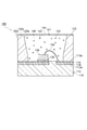
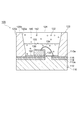
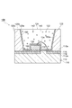
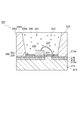
- FIG. 1 is a cross-sectional view of an optical semiconductor device according to a first embodiment.
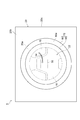
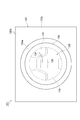
- FIG. 2 is a plan view of the optical semiconductor device shown in FIG. 1. It is a conceptual diagram for demonstrating the structure of the sulfide prevention film
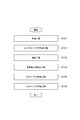
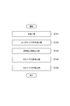
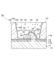
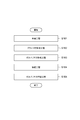
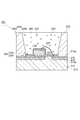
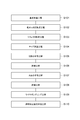
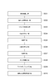
- FIG. 10 is a flowchart illustrating a method for manufacturing an optical semiconductor device according to a fifth embodiment. It is a figure which shows the manufacturing process of the optical semiconductor device which concerns on 5th Embodiment. It is a figure which shows the manufacturing process of the optical semiconductor device which concerns on 5th Embodiment. It is sectional drawing of the optical semiconductor device which concerns on 6th Embodiment. 10 is a flowchart illustrating a method for manufacturing an optical semiconductor device according to a sixth embodiment.
- FIG. It is a top view of the light-emitting device shown in FIG. It is a schematic diagram which shows an example of a layered silicic acid compound. It is the flowchart which showed the manufacturing method of the light-emitting device which concerns on 11th and 12th embodiment. It is sectional drawing of the light-emitting device after the application
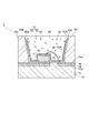
- FIG. 1 is a cross-sectional view of the optical semiconductor device according to the first embodiment.
- FIG. 2 is a plan view of the optical semiconductor device shown in FIG.
- the optical semiconductor device 1 according to the embodiment is generally classified as a “surface mount type”.
- the optical semiconductor device 1 is filled in a substrate 10, a blue light emitting diode 30 bonded to the surface of the substrate 10, a reflector 20 provided on the surface of the substrate 10 so as to surround the blue light emitting diode 30, and the reflector 20.
- the transparent sealing portion 40 that seals the blue light emitting diode 30 and the silver sulfide prevention film 70 that covers the silver plating layer 16 are provided.
- illustration of the transparent sealing part 40 is abbreviate
- a copper plating plate 14 is wired on the surface of an insulating base 12, and a silver plating layer 16 is formed on the surface of the copper plating plate 14.
- the silver plating layer 16 is an electrode that is disposed on the surface of the substrate 10 and is electrically connected to the blue light emitting diode 30.
- the silver plating layer 16 may have any composition as long as it is a plating layer containing silver.
- the silver plating layer 16 may be formed by plating only silver, or the silver plating layer 16 may be formed by plating nickel and silver in this order.
- the copper plating plate 14 and the silver plating layer 16 are insulated on the anode side and the cathode side.
- the insulation between the copper plating plate 14 and the silver plating layer 16 on the anode side and the copper plating plate 14 and the silver plating layer 16 on the cathode side is, for example, the copper plating plate 14 and the silver plating layer 16 on the anode side and the cathode side.
- the copper plating plate 14 and the silver plating layer 16 can be separated from each other, and an insulating layer such as a resin and ceramic can be appropriately inserted therebetween.
- the blue light emitting diode 30 is die-bonded to the silver plating layer 16 on either the anode side or the cathode side, and is electrically connected to the silver plating layer 16 through the die bonding material 32.
- the blue light emitting diode 30 is wire-bonded to the other silver plating layer 16 on the anode side or the cathode side, and is electrically connected to the silver plating layer 16 through the bonding wire 34.
- the reflector 20 is a light reflecting portion that fills the transparent sealing portion 40 for sealing the blue light emitting diode 30 and reflects the light emitted from the blue light emitting diode 30 to the surface side of the optical semiconductor device 1.
- the reflector 20 is erected from the surface of the substrate 10 so as to surround the blue light emitting diode 30, and forms an inner space 22 that accommodates the blue light emitting diode 30 inside.
- the reflector 20 includes a light reflecting surface 20a, a top surface 20b, and an outer peripheral surface 20c.
- the light reflecting surface 20 a is formed in a circular shape in plan view (see FIG. 2), and forms an inner space 22 that surrounds the blue light emitting diode 30 and accommodates the blue light emitting diode 30.
- the inner space 22 that accommodates the blue light emitting diode 30 is formed by the light reflecting surface 20 a surrounding the blue light emitting diode 30.
- the top surface 20b is located outside the inner space 22 adjacent to the light reflecting surface 20a, and spreads from the front side edge of the light reflecting surface 20a toward the opposite side of the inner space 22.
- the outer peripheral surface 20c is formed in a rectangular shape in plan view (see FIG. 2), and rises from the surface 10a of the substrate 10 to the outer edge of the top surface 20b.
- the shapes of the light reflecting surface 20 a and the outer peripheral surface 20 c are not particularly limited.
- the light reflecting surface 20 a has a truncated cone shape (funnel) whose diameter increases as the distance from the substrate 10 increases.
- the outer peripheral surface 20 c is preferably formed in a rectangular shape perpendicular to the substrate 10 from the viewpoint of improving the degree of integration of the optical semiconductor device 1.
- the lower portion located on the substrate 10 side is perpendicular to the substrate 10, and the upper portion located on the opposite side of the substrate 10 is separated from the substrate 10. An enlarged diameter is shown.
- the reflector 20 is made of a cured product of a thermosetting resin composition containing a white pigment.
- the thermosetting resin composition is preferably one that can be pressure-molded at room temperature (25 ° C.) before thermosetting.
- thermosetting resin contained in the thermosetting resin composition various resins such as an epoxy resin, a silicone resin, a urethane resin, and a cyanate resin can be used.
- an epoxy resin is preferable because of its excellent adhesion to various materials.
- the white pigment alumina, magnesium oxide, antimony oxide, titanium oxide, zirconium oxide or the like can be used. Among these, titanium oxide is preferable from the viewpoint of light reflectivity.
- Inorganic hollow particles may be used as the white pigment. Specific examples of the inorganic hollow particles include sodium silicate glass, aluminum silicate glass, borosilicate soda glass, and shirasu.
- the transparent sealing part 40 is filled in the inner space 22 formed by the light reflecting surface 20a of the reflector 20, and seals the blue light emitting diode 30.
- This transparent sealing part 40 consists of transparent sealing resin which has translucency.
- the transparent sealing resin includes a translucent resin as well as a completely transparent resin.
- the transparent sealing resin preferably has an elastic modulus of 1 MPa or less at room temperature (25 ° C.). In particular, it is preferable to employ a silicone resin or an acrylic resin from the viewpoint of transparency.
- the transparent sealing resin may further contain a phosphor 42 that converts white light into an inorganic filler that diffuses light or blue light emitted from the blue light emitting diode 30 as an excitation source.
- the silver sulfide prevention film 70 has a gas barrier layer 50 having a gas barrier property by clay, and a primer layer 60 that is disposed under the gas barrier layer 50 and has an adhesive property.
- the gas barrier layer 50 suppresses sulfidation of the silver plating layer 16 by covering the silver plating layer 16.
- the gas barrier layer 50 is a layer containing clay.
- any of natural clay and synthetic clay can be used.
- any one or more of stevensite, hectorite, saponite, montmorillonite and beidellite can be used.
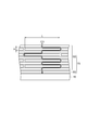
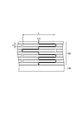
- natural clay montmorillonite as shown in FIG. 3, has a high aspect ratio such as a thickness H of 1 nm or less and a length L of 10 nm or more and 400 nm or less, and has a long gas path route.
- the film thickness of the gas barrier layer 50 is preferably 0.01 ⁇ m or more and 1000 ⁇ m or less, more preferably 0.03 ⁇ m or more and 500 ⁇ m or less, further preferably 0.05 ⁇ m or more and 100 ⁇ m or less, and 0.05 ⁇ m or more.
- the thickness is more preferably 10 ⁇ m or less, and further preferably 0.05 ⁇ m or more and 1 ⁇ m or less.
- this effect can be further improved by setting the thickness of the gas barrier layer 50 to 0.03 ⁇ m to 500 ⁇ m, 0.05 ⁇ m to 100 ⁇ m, 0.05 ⁇ m to 10 ⁇ m, 0.05 ⁇ m to 1 ⁇ m. it can.
- the primer layer 60 is arranged between the reflector 20 and the transparent sealing portion 40 to suppress peeling of the transparent sealing portion 40 with respect to the reflector 20.
- the primer layer 60 is preferably a layer having adhesiveness and insulating properties, and for example, a layer containing a silicate compound can be used.
- the silicic acid compound include silicone resins such as silicone rubber and inorganic glass.
- the silicic acid compound used in this embodiment preferably has a linear expansion coefficient of 180 ppm to 450 ppm from the viewpoint of obtaining adhesiveness due to its flexibility.
- the linear expansion coefficient is 180 ppm or more, it becomes easy to ensure adhesiveness due to flexibility.
- the linear expansion coefficient is 450 ppm or less, for example, a transparent sealing resin used for coating or sealing Thus, deformation of the primer layer can be suppressed.
- the silicic acid compound preferably has a linear expansion coefficient of 200 ppm to 450 ppm, and from the viewpoint of enhancing the adhesion reliability with the transparent sealing resin used for coating or sealing, 200 ppm. More preferably, it is ⁇ 350 ppm.
- the silicic acid compound used in the present embodiment preferably has a volume resistivity of 10 10 to 10 16 ⁇ ⁇ cm from the viewpoint of ensuring insulation, and 10 12 to 10 16 ⁇ ⁇ cm from the viewpoint of improving insulation. Are more preferable, and those of 10 13 to 10 16 ⁇ ⁇ cm are more preferable.
- the volume resistivity of a silicate compound means the value measured according to JISC2139 about the volume resistivity measurement test piece obtained by apply
- the thickness of the primer layer 60 is preferably 10 nm to 1000 nm from the viewpoint of adhesion, more preferably 30 nm to 1000 nm from the viewpoint of water resistance, and further 30 to 500 nm from the viewpoint of effectively expressing the gas barrier properties of the gas barrier layer 50. preferable.
- the gas barrier layer 50 can be formed by dropping or spreading a clay diluted solution obtained by diluting the above clay with a solvent into the inner space 22 of the reflector 20 and then removing and / or curing the solvent.
- the primer layer 60 can be formed by dropping or dispersing a primer diluted solution obtained by diluting the above-described silicate compound with a solvent into the inner space 22 of the reflector 20 and then removing and / or curing the solvent.
- the gas barrier layer 50 on the primer layer 60, while ensuring transparency, the water resistance of the silver sulfide prevention film 70 and the adhesive force to the silver plating layer 16 can be improved, Peeling between the transparent sealing portion 40 used for sealing and the light reflecting surface 20a can be suppressed.
- the specific arrangement of the gas barrier layer 50 and the primer layer 60 is as follows.
- the primer layer 60 is formed on the entire surface of the silver plating layer 16 and the light reflection surface 20a, and the gas barrier layer 50 covers a part of the silver plating layer 16 and the light reflection surface 20a.
- a portion of the primer layer 60 that is formed on the light reflecting surface 20a is referred to as a primer layer reflecting surface portion 60a.
- the primer layer reflecting surface portion 60 a is formed with a covering portion where the gas barrier layer 50 is laminated and an exposed portion U where the gas barrier layer 50 is not laminated, and the transparent sealing portion 40 is in contact with the exposed portion U of the primer layer 60. is doing.
- the gas barrier layer 50 only needs to cover the silver plating layer 16, and may or may not cover the blue light emitting diode 30.
- the ratio of the area of the exposed portion U to the primer layer reflecting surface portion 60a (hereinafter referred to as “the ratio of the area of the exposed portion U”) is not particularly limited, but is preferably 1 to 99%, and is preferably 5 to 95. % Is more preferable, and 10 to 90% is particularly preferable.
- the ratio of the area of the exposed portion U is not particularly limited, but is preferably 1 to 99%, and is preferably 5 to 95. % Is more preferable, and 10 to 90% is particularly preferable.
- the gas barrier layer 50 using the above-described clay has sufficient translucency as long as the film thickness is 0.01 ⁇ m or more and 1000 ⁇ m or less. For this reason, even if the light reflection surface 20a is covered with the gas barrier layer 50, the reflection characteristics of the reflector 20 are not greatly affected. Moreover, a thin film of montmorillonite, which is a natural clay, has an action of amplifying the blue light frequency band. For this reason, the reflection efficiency of the blue light emitted from the blue light emitting diode 30 is increased by covering the light reflecting surface 20a with the gas barrier layer 50 using montmorillonite which is natural clay.
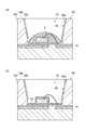
- FIG. 4 is a diagram for explaining a method for forming a primer layer.
- FIG. 5 is a diagram for explaining a gas barrier layer coating method.
- the primer diluted solution M is dropped or dispersed in the inner space 22 of the reflector 20.
- the dripping amount or the spraying amount of the primer diluent M is adjusted to cover the entire surface of the light reflecting surface 20a with the primer diluent M.
- the solvent of the primer diluent M is dried.
- the primer layer 60 is formed on the entire surface covered with the primer diluent M, that is, on the entire surface of the silver plating layer 16, the blue light emitting diode 30, and the light reflecting surface 20a.
- the clay diluted solution L is dropped or spread on the inner space 22 of the reflector 20 as shown in FIG.
- all of the silver plating layer 16 is covered with the clay diluent L and a part of the light reflecting surface 20a is covered with the clay diluent L (a part of the light reflecting surface 20a is covered with the clay diluent L.
- the dripping amount or the spraying amount of the clay diluent L is adjusted.
- the solvent of the clay diluent L is dried. Then, as shown in FIG.
- the gas barrier layer 50 is formed on the entire surface covered with the clay diluent L, that is, on a part of the silver plating layer 16, the blue light emitting diode 30, and the primer layer reflecting surface portion 60a. It is laminated on the primer layer 60.
- the transparent sealing portion 40 containing the phosphor 42 is filled into the inner space 22, and the blue light emitting diode 30 is sealed with the transparent sealing portion 40. To do.
- the transparent sealing portion 40 contacts the exposed portion U in the primer layer reflecting surface portion 60a. Thereby, the optical semiconductor device 1 in which the exposed portion U which is a part of the light reflecting surface 20a and the transparent sealing portion 40 are joined is obtained.
- the silver plating layer 16 is covered with the gas barrier layer 50 having the gas barrier property by clay, the sulfidation of the silver plating layer 16 can be suppressed. . Thereby, the illumination intensity fall of the optical semiconductor device 1 by the silver plating layer 16 blackening can be suppressed significantly.
- an adhesive primer layer is disposed under the gas barrier layer 50, and the transparent sealing portion 40 is brought into contact with the primer layer 60, whereby the primer layer 60 is not present or the primer layer. Compared with the case where 60 and transparent sealing resin are not contacting, it can suppress that the transparent sealing part 40 peels.
- the inner space 22 is small, it is difficult to drop or spray the clay diluent L and the primer diluent M only on the silver plating layer 16. Therefore, by allowing the gas barrier layer 50 and the primer layer 60 to cover the light reflecting surface 20a, the coating of the gas barrier layer 50 and the primer layer 60 on the silver plating layer 16 can be easily performed. Moreover, even in this case, since the transparent sealing portion 40 and the primer layer 60 are in contact with each other at the exposed portion U of the primer layer reflecting surface portion 60a, it is possible to suppress the peeling of the transparent sealing portion 40. it can.
- the light reflecting surface 20a reflects the light generated from the blue light emitting diode 30 and outputs it from the optical semiconductor device 1, but the gas barrier layer 50 having a gas barrier property of clay amplifies the frequency band of blue light. Therefore, the reflection efficiency of the blue light generated from the blue light emitting diode 30 can be increased by covering the light reflecting surface 20a with the gas barrier layer 50.
- the second embodiment is basically the same as the first embodiment, and only the formation position of the gas barrier layer is different from the first embodiment. For this reason, in the following description, only matters different from the first embodiment will be described, and the same description as in the first embodiment will be omitted.
- FIG. 6 is a cross-sectional view of an optical semiconductor device according to the second embodiment.
- the optical semiconductor device 2 according to the second embodiment includes a silver sulfide prevention film 72 instead of the silver sulfide prevention film 70 of the first embodiment.
- the silver sulfide prevention film 72 includes a gas barrier layer 52 and a primer layer 60.
- the gas barrier layer 52 is basically the same as the gas barrier layer 50, but differs from the gas barrier layer 50 in that it does not cover the light reflecting surface 20a. That is, the gas barrier layer 52 is not laminated on the primer layer reflection surface portion 60 a, and the entire surface of the primer layer reflection surface portion 60 a is exposed to the gas barrier layer 52. For this reason, the transparent sealing part 40 is in contact with the entire surface of the primer layer reflection surface part 60a.
- the gas barrier layer 52 only needs to cover the silver plating layer 16, and may or may not cover the blue light emitting diode 30.
- FIG. 7 is a diagram for explaining a gas barrier layer coating method.
- the clay diluent L is dropped or spread on the inner space 22 of the reflector 20.
- the entire surface of the silver plating layer 16 is covered with the clay diluent L, but the dripping amount or the dispersion of the clay diluent L so that the light reflecting surface 20a and the primer layer reflecting surface portion 60a are not covered with the clay diluent L. Adjust the amount.
- the solvent of the clay diluent L is dried. Then, as shown in FIG.
- the gas barrier layer 52 is formed on the entire surface covered with the clay diluent L, that is, on the entire surface of the silver plating layer 16, the blue light emitting diode 30, and the primer layer reflecting surface portion 60a. Laminated on layer 60.
- the gas barrier layer 52 is not stacked on the primer layer 60 on the light reflecting surface 20a, so that the contact area between the transparent sealing portion 40 and the primer layer 60 can be increased. Therefore, it can further suppress that the transparent sealing part 40 peels.
- the third embodiment is basically the same as the first embodiment, and is different from the first embodiment only in the formation positions of the primer layer and the gas barrier layer. For this reason, in the following description, only matters different from the first embodiment will be described, and the same description as in the first embodiment will be omitted.
- FIG. 8 is a cross-sectional view of an optical semiconductor device according to the third embodiment.
- the optical semiconductor device 3 according to the third embodiment includes a silver sulfide prevention film 73 instead of the silver sulfide prevention film 70 of the first embodiment.
- the silver sulfide prevention film 73 includes a primer layer 63 and a gas barrier layer 53.
- the primer layer 63 is basically the same as the primer layer 60, but is different from the primer layer 60 in that it is not formed on the entire surface of the light reflecting surface 20a.
- a portion of the primer layer 63 formed on the light reflecting surface 20a is referred to as a primer layer reflecting surface portion 63a.
- the edge part by the side of the top surface 20b among the light reflection surfaces 20a is called upper end part 20d.
- the primer layer 63 is formed only in the part except the upper end part 20d among the light reflection surfaces 20a, and the primer layer 63 is not formed in this upper end part 20d. That is, the primer layer reflection surface portion 63a extends from the silver plating layer 16 to the front of the top surface 20b along the light reflection surface 20a.
- the gas barrier layer 53 is basically the same as the gas barrier layer 50, but is different from the gas barrier layer 50 in that the gas barrier layer 53 is laminated on substantially the entire primer layer reflecting surface portion 63a on the light reflecting surface 20a.
- the tip surface 63b of the primer layer reflecting surface portion 43a extending along the light reflecting surface 20a, that is, the tip surface 63b on the top surface 20b side of the primer layer reflecting surface portion 43a is exposed from the gas barrier layer 53, and this tip surface 63b and the transparent sealing part 40 are contacting.
- the clay diluent L is placed inside so that the front end surface 63b is not covered with the clay diluent L.
- the method of dripping or spraying to the space 22 and drying the solvent of the clay dilution L is mentioned.
- the tip surface 63b of the primer layer reflecting surface portion 43a extending along the light reflecting surface 20a
- the fourth embodiment is basically the same as the first embodiment, and is different from the first embodiment only in the formation positions of the primer layer, the gas barrier layer, and the transparent sealing resin. For this reason, in the following description, only matters different from the first embodiment will be described, and the same description as in the first embodiment will be omitted.
- FIG. 9 is a cross-sectional view of an optical semiconductor device according to the fourth embodiment.
- the optical semiconductor device 4 according to the fourth embodiment includes a primer layer 64, a gas barrier layer 54, and a primer layer 60, a gas barrier layer 50, and a transparent sealing portion 40 according to the first embodiment.
- a transparent sealing resin 44 is provided.
- the primer layer 64 is basically the same as the primer layer 60, but differs from the primer layer 60 in that it is formed from the light reflecting surface 20a to the top surface 20b.
- a portion formed on the light reflecting surface 20a is referred to as a primer layer reflecting surface portion 64a
- a portion formed on the top surface 20b is referred to as a primer layer top surface portion 64b.
- the gas barrier layer 54 is basically the same as the gas barrier layer 50, but is different from the gas barrier layer 50 in that the gas barrier layer 54 is laminated on the entire primer layer reflecting surface portion 64a. However, the gas barrier layer 54 does not cover the primer layer top surface portion 64b. For this reason, the primer layer top surface portion 64 b is exposed from the gas barrier layer 54.
- the transparent sealing resin 44 is basically the same as the transparent sealing portion 40, but reaches the top surface 20 b beyond the inner space of the reflector 20.
- the transparent sealing resin 44 seals the primer layer top surface portion 64b while being in contact with the primer layer top surface portion 64b.
- the primer layer top surface portion 64b is formed and transparently sealed with the primer layer top surface portion 64b.
- the transparent sealing resin 44 can be prevented from peeling off.
- the inner space 22 is small, it is difficult to drop or spray the clay diluent L and the primer diluent M only on the silver plating layer 16. Therefore, by allowing the gas barrier layer 54 and the primer layer 64 to cover the entire surface of the light reflecting surface 20a, the coating of the gas barrier layer 54 and the primer layer 64 on the silver plating layer 16 can be easily performed. Moreover, even in this case, since the transparent sealing portion 40 and the primer layer top surface portion 64b are in contact with each other, the transparent sealing portion 40 can be prevented from peeling off.
- the base 12 and the reflector 20 are described as separate members, but may be formed integrally.
- the optical semiconductor device 101 As shown in FIGS. 10 and 11, the optical semiconductor device 101 according to the embodiment is generally classified as a “surface mount type”.
- the optical semiconductor device 101 is filled in a substrate 110, a blue light emitting diode 130 bonded to the surface of the substrate 110, a reflector 120 provided on the surface of the substrate 110 so as to surround the blue light emitting diode 130, and the reflector 120.
- the transparent sealing portion 140 that seals the blue light emitting diode 130 and the gas barrier layer 150 that covers the silver plating layer 116 are provided.
- illustration of the transparent sealing part 140 is abbreviate
- “covering the silver plating layer 116” means covering the silver plating layer 116 directly or indirectly.
- To indirectly cover the silver plating layer 116 means to cover the silver plating layer 116 with another member between the silver plating layer 116, for example.
- a copper plating plate 114 is wired on the surface of an insulating base 112, and a silver plating layer 116 is formed on the surface of the copper plating plate 114.
- the silver plating layer 116 is an electrode that is disposed on the surface of the substrate 110 and is electrically connected to the blue light emitting diode 130.
- the silver plating layer 116 may have any composition as long as it is a plating layer containing silver.
- the silver plating layer 116 may be formed by plating only silver, or the silver plating layer 116 may be formed by plating nickel and silver in this order.
- the copper plating plate 114 and the silver plating layer 116 are insulated on the anode side and the cathode side.
- the insulation between the copper plating plate 114 and the silver plating layer 116 on the anode side and the copper plating plate 114 and the silver plating layer 116 on the cathode side is, for example, the copper plating plate 114 on the anode side and the silver plating layer 116 on the cathode side.
- the copper plating plate 114 and the silver plating layer 116 can be separated from each other, and an insulating layer such as a resin and ceramic can be appropriately inserted therebetween.
- the blue light emitting diode 130 is die-bonded to any one of the silver plating layer 116 on the anode side and the cathode side, and is electrically connected to the silver plating layer 116 through the die bonding material 132.
- the blue light emitting diode 130 is wire-bonded to the silver plating layer 116 on either the anode side or the cathode side, and is electrically connected to the silver plating layer 116 through the bonding wire 134.
- the reflector 120 is a light reflecting portion that fills the transparent sealing portion 140 for sealing the blue light emitting diode 130 and reflects the light emitted from the blue light emitting diode 130 to the surface side of the optical semiconductor device 101.
- the reflector 120 is erected from the surface of the substrate 110 so as to surround the blue light emitting diode 130, and forms an inner space 122 that accommodates the blue light emitting diode 130 inside. For this reason, the opposite side of the substrate 110 in the inner space 122 is an opening 124 of the inner space 122.
- the reflector 120 includes a light reflecting surface 120a, a top surface 120b, and an outer peripheral surface 120c.
- the light reflecting surface 120a is formed in a circular shape in plan view (see FIG.
- the inner space 122 that accommodates the blue light emitting diode 130 is formed by the light reflecting surface 120 a surrounding the blue light emitting diode 130.
- the top surface 120b is located outside the inner space 122 adjacent to the light reflecting surface 120a, and spreads from the front edge of the light reflecting surface 120a toward the opposite side of the inner space 122.
- the outer peripheral surface 120c is formed in a rectangular shape in plan view (see FIG. 11), and rises from the surface 110a of the substrate 110 to the outer edge of the top surface 120b.
- the shapes of the light reflecting surface 120 a and the outer peripheral surface 120 c are not particularly limited, but from the viewpoint of improving the illuminance of the optical semiconductor device 101, the light reflecting surface 120 a has a truncated cone shape (funnel) whose diameter increases as the distance from the substrate 110 increases. From the viewpoint of improving the degree of integration of the optical semiconductor device 101, the outer peripheral surface 120c is preferably formed in a rectangular shape perpendicular to the substrate 110. In the drawing, as an example of forming the light reflecting surface 120a, the lower portion located on the substrate 110 side is perpendicular to the substrate 110, and the upper portion located on the opposite side of the substrate 110 is separated from the substrate 110. An enlarged diameter is shown.
- the reflector 120 is made of a cured product of a thermosetting resin composition containing a white pigment.
- the thermosetting resin composition is preferably one that can be pressure-molded at room temperature (25 ° C.) before thermosetting.
- thermosetting resin contained in the thermosetting resin composition various resins such as an epoxy resin, a silicone resin, a urethane resin, and a cyanate resin can be used.
- an epoxy resin is preferable because of its excellent adhesion to various materials.
- the white pigment alumina, magnesium oxide, antimony oxide, titanium oxide, zirconium oxide or the like can be used. Among these, titanium oxide is preferable from the viewpoint of light reflectivity.
- Inorganic hollow particles may be used as the white pigment. Specific examples of the inorganic hollow particles include sodium silicate glass, aluminum silicate glass, borosilicate soda glass, and shirasu.
- the transparent sealing part 140 is filled in the inner space 122 formed by the light reflecting surface 120a of the reflector 120, and seals the blue light emitting diode 130.
- the transparent sealing portion 140 is made of a transparent sealing resin having translucency.
- the transparent sealing resin includes a translucent resin as well as a completely transparent resin.
- the transparent sealing resin preferably has an elastic modulus of 1 MPa or less at room temperature (25 ° C.). In particular, it is preferable to employ a silicone resin or an acrylic resin from the viewpoint of transparency.
- the transparent sealing resin may further contain an inorganic filler that diffuses light or a phosphor 42 that emits white light using blue light emitted from the blue light emitting diode 130 as an excitation source.
- the gas barrier layer 150 is a gas barrier layer having a gas barrier property by clay, and suppresses sulfidation of the silver plating layer 116 by covering the silver plating layer 116.
- the gas barrier layer 150 is disposed at a position away from the substrate 110 and covers the silver plating layer 116 from the opening 124 side of the inner space 122.
- the gas barrier layer 150 is embedded in the transparent sealing part 140, and the front and back surfaces of the gas barrier layer 150 are sealed in the transparent sealing part 140. Further, the gas barrier layer 150 is connected to the entire circumference surrounding the inner space 122 of the light reflecting surface 120a, and the transparent sealing portion 140 is divided into a portion on the substrate 110 side and a portion on the opening 124 side by the gas barrier layer 150. It has been. For this reason, the transparent sealing part 140, the gas barrier layer 150, and the transparent sealing part 140 are laminated
- the gas barrier layer 150 is a layer containing clay.
- the clay constituting the gas barrier layer 150 any of natural clay and synthetic clay can be used.
- any one or more of stevensite, hectorite, saponite, montmorillonite and beidellite can be used.
- natural clay montmorillonite has a high aspect ratio such as a thickness H of 1 nm or less and a length L of 10 nm or more and 400 nm or less, and has a long gas path route, and thus has excellent gas barrier properties.
- the layer thickness of the gas barrier layer 150 is preferably 0.01 ⁇ m or more and 1000 ⁇ m or less, more preferably 0.03 ⁇ m or more and 500 ⁇ m or less, further preferably 0.05 ⁇ m or more and 100 ⁇ m or less, and 0.05 ⁇ m or more. It is more preferably 10 ⁇ m or less, and further preferably 0.05 ⁇ m or more and 1 ⁇ m or less.
- this effect can be further improved by setting the layer thickness of the gas barrier layer 150 to 0.03 ⁇ m to 500 ⁇ m, 0.05 ⁇ m to 100 ⁇ m, 0.05 ⁇ m to 10 ⁇ m, 0.05 ⁇ m to 1 ⁇ m. it can.
- the gas barrier layer 150 using the above-mentioned clay has sufficient translucency if the layer thickness is 0.01 ⁇ m or more and 1000 ⁇ m or less. For this reason, even if the gas reflection layer 120a is covered with the gas barrier layer 150, the reflection characteristics of the reflector 120 are not greatly affected.
- a thin film of montmorillonite which is a natural clay, has an action of amplifying the blue light frequency band. For this reason, the reflection efficiency of the blue light emitted from the blue light emitting diode 130 increases by covering the light reflection surface 120a with the gas barrier layer 150 using the natural clay montmorillonite.
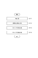
- FIG. 13 is a flowchart showing a method for manufacturing an optical semiconductor device according to the fifth embodiment.
- FIG. 14 and FIG. 15 are diagrams illustrating manufacturing steps of the optical semiconductor device according to the fifth embodiment.
- the substrate 110 having a silver plating layer 116 formed on the surface, the blue light emitting diode 130 bonded to the silver plating layer 116, and the blue light emitting diode 130 are surrounded.
- a preparatory step (S111) for preparing the intermediate component 108 including the reflector 120 that forms the inner space 122 that accommodates the blue light emitting diode 130 by the light reflecting surface 120a is performed.
- the transparent sealing portion 140 containing the phosphor 142 is filled into the inner space 122, and the blue light emitting diode 130 is sealed with the transparent sealing portion 140.
- the transparent sealing part sealing process (S112) to stop is performed.
- the filling amount of the transparent sealing portion 140 is adjusted so that the transparent sealing portion 140 is filled to about half of the inner space 122.
- the bonding wire 134 may or may not be sealed with the transparent sealing portion 140.
- the transparent sealing portion 140 is cured by drying or the like.
- a gas barrier layer forming step (S113) for forming the gas barrier layer 150 at a position away from the substrate 110 is performed.
- the clay dilution liquid L is dropped or dispersed in the inner space 122 filled with the transparent sealing portion 140.
- the dripping amount or spraying amount of the clay diluent L is adjusted so that the clay diluent L covers the entire surface of the transparent sealing portion 140 and contacts the entire circumference surrounding the inner space 122 of the light reflecting surface 120a.
- the solvent of the clay diluent L is dried.
- the gas barrier layer 150 connected to the entire circumference of the light reflecting surface 120a is formed on the entire surface of the transparent sealing portion 140.
- the silver plating layer 116 is covered with the gas barrier layer 150 from the opening 124 side through the transparent sealing portion 140.
- a burying step (S114) is performed. Thereby, the gas barrier layer 150 is embedded in the transparent sealing portion 140, and the transparent sealing portion 140, the gas barrier layer 150, and the transparent sealing portion 140 are laminated in this order on the silver plating layer 116.
- the gas barrier layer 150 having the gas barrier property by clay
- the sulfidation of the silver plating layer 116 can be suppressed.
- the illumination intensity fall of the optical semiconductor device 101 by the silver plating layer 116 blackening can be suppressed significantly.
- the gas barrier layer which has the gas barrier property by clay increases gas barrier property by equalizing the layer thickness.
- the surface of the substrate 110 on which the silver plating layer 116 is formed is uneven, if a gas barrier layer is formed on the surface of the substrate 110, it is difficult to make the thickness of the gas barrier layer uniform. Therefore, by arranging the gas barrier layer 150 at a position away from the substrate 110, the thickness of the gas barrier layer 150 can be made uniform. Thereby, the gas barrier property of the gas barrier layer 150 can be improved.
- gas barrier layer 150 is separated from the substrate 110 by disposing the transparent sealing portion 140 between the gas barrier layer 150 and the substrate 110, migration between the gas barrier layer 150 and the substrate 110 is prevented. can do.
- the gas barrier layer 150 is embedded in the transparent sealing portion 140, it is possible to prevent the gas barrier layer 150 from being peeled off.
- the sixth embodiment is basically the same as the fifth embodiment, and only the formation position of the gas barrier layer is different from the fifth embodiment. For this reason, in the following description, only matters different from the fifth embodiment will be described, and description similar to that of the fifth embodiment will be omitted.
- FIG. 16 is a cross-sectional view of an optical semiconductor device according to the sixth embodiment.
- the optical semiconductor device 102 according to the sixth embodiment includes a gas barrier layer 151 formed on the surface of the transparent sealing portion 140 instead of the gas barrier layer 150 of the fifth embodiment. Yes.
- the gas barrier layer 151 is a gas barrier layer having a gas barrier property by clay, like the gas barrier layer 150 of the fifth embodiment, and suppresses the sulfidation of the silver plating layer 116 by covering the silver plating layer 116.
- the gas barrier layer 151 is disposed at a position away from the substrate 110 and covers the silver plating layer 116 from the opening 124 side of the inner space 122.
- the gas barrier layer 151 is formed on the surface of the transparent sealing portion 140 and the top surface 120b of the reflector 120, and is connected to the entire circumference surrounding the inner space 122 of the top surface 120b so as to cover the entire inner space 122. ing.
- the transparent sealing portion 140 and the gas barrier layer 151 are laminated in this order on the silver plating layer 116 toward the opening 124.
- the material, configuration, layer thickness, etc. of the gas barrier layer 151 are the same as those of the gas barrier layer 150 of the fifth embodiment.
- FIG. 17 is a flowchart showing a method for manufacturing an optical semiconductor device according to the sixth embodiment.
- a preparation step (S121) similar to that of the fifth embodiment is performed.
- the transparent sealing portion 140 including the phosphor 142 is filled in the inner space 122, and the transparent sealing portion sealing step (S122) for sealing the blue light emitting diode 130 with the transparent sealing portion 140 is performed. . At this time, the filling amount of the transparent sealing portion 140 is adjusted so that the transparent sealing portion 140 is filled in the entire inner space 122.
- a gas barrier layer forming step (S123) for forming the gas barrier layer 151 at a position away from the substrate 110 is performed.
- a clay diluted solution is dropped or spread on the surface of the transparent sealing portion 140 and the top surface 120b of the reflector 120.
- the dripping amount or the spraying amount of the clay diluent is adjusted so that the clay diluent covers the entire surface of the transparent sealing portion 140 and contacts the entire circumference surrounding the inner space 122 of the top surface 120b.
- the solvent of the clay diluent is dried.
- the gas barrier layer 151 connected to the entire circumference of the top surface 120b is formed on the entire surface of the transparent sealing portion 140.
- the silver plating layer 116 is covered with the gas barrier layer 151 via the transparent sealing portion 140 from the opening 124 side.
- the gas barrier layer 151 is formed on the surface of the transparent sealing portion 140, the transparent sealing portion 140 and the gas barrier layer 151 can be easily formed. Can do.
- the seventh embodiment is basically the same as the fifth embodiment, and differs from the fifth embodiment only in that a second gas barrier layer is newly provided. For this reason, in the following description, only matters different from the fifth embodiment will be described, and description similar to that of the fifth embodiment will be omitted.
- FIG. 18 is a cross-sectional view of an optical semiconductor device according to the seventh embodiment.
- the optical semiconductor device 103 according to the seventh embodiment is the one in which a second gas barrier layer 152 is newly added to the optical semiconductor device 101 according to the fifth embodiment.
- the second gas barrier layer 152 is a gas barrier layer having a gas barrier property by clay, and suppresses sulfidation of the silver plating layer 116 by covering the silver plating layer 116. is there.
- the second gas barrier layer 152 is formed on the surface of the substrate 110 (silver plating layer 116), and covers the silver plating layer 116 from the opening 124 side of the inner space 122. For this reason, the second gas barrier layer 152 is directly laminated on the silver plating layer 116.
- the second gas barrier layer 152, the transparent sealing portion 140, the gas barrier layer 150, and the transparent sealing portion 140 are stacked in this order on the silver plating layer 116 toward the opening 124.
- the material, configuration, layer thickness, etc. of the second gas barrier layer 152 are the same as those of the gas barrier layer 150 of the fifth embodiment.
- FIG. 19 is a flowchart showing a method for manufacturing an optical semiconductor device according to the seventh embodiment.
- a preparation step (S131) of preparing an intermediate part including the inner space 122 that accommodates the blue light emitting diode 130 and the reflector 120 is performed.
- an intermediate part in which the blue light emitting diode 130 and the silver plating layer 116 are not wire-bonded is prepared.
- a second gas barrier layer forming step (S132) for forming the second gas barrier layer 152 on the surface of the silver plating layer 116 is performed.
- a clay diluent is dropped or spread on the inner space 122.
- the dripping amount or the spraying amount of the clay dilution solution is adjusted so that the clay dilution solution covers the entire surface of the substrate 110 exposed in the inner space 122 and contacts the entire circumference surrounding the inner space 122 of the light reflecting surface 120a. Adjust. Thereafter, the solvent of the clay diluent is dried.
- the second gas barrier layer 152 connected to the entire circumference surrounding the inner space 122 of the light reflecting surface 120a is formed on the entire surface of the substrate 110 exposed to the inner space 122.
- the silver plating layer 116 is covered with the second gas barrier layer 152 from the opening 124 side.
- connection step (S133) is performed in which the blue light emitting diode 130 and the silver plating layer 116 covered with the second gas barrier layer 152 are electrically connected by wire bonding.
- a well-known apparatus can be used for the wire bonding apparatus used for this connection process.
- the wire bonding apparatus includes a capillary (not shown) through which the bonding wire 134 is inserted. The capillary is moved to a predetermined position and then lowered, and the bonding wire 134 is fixed by pressing the bonding wire 134 against the blue light emitting diode 130 or the silver plating layer 116 on which the second gas barrier layer 152 is formed.
- the bonding wire 134 is fixed to the blue light emitting diode 130 or the silver plating layer 116. That is, a load of about 60 g to 150 gf is applied to the capillary, or the capillary is vibrated in a frequency band of 80 kHz to 160 kHz. Thereby, the blue light emitting diode 130 and the silver plating layer 116 are electrically connected to each other by the bonding wire 134.
- the transparent sealing portion 140 including the phosphor 142 is filled into the inner space 122 in which the second gas barrier layer 152 is formed, and the transparent LED 140 is sealed with the transparent sealing portion 140.
- a stop part sealing process (S134) is performed.
- the filling amount of the transparent sealing portion 140 is adjusted so that the transparent sealing portion 140 is filled to about half of the inner space 122.
- the bonding wire 134 may or may not be sealed with the transparent sealing portion 140.
- the transparent sealing portion 140 is cured by drying or the like.
- a gas barrier layer forming step for forming the gas barrier layer 150 at a position away from the substrate 110 is performed.
- the clay diluent is dropped or spread on the inner space 122 filled with the transparent sealing portion 140.
- the dripping amount or the spraying amount of the clay diluent is adjusted so that the clay diluent covers the entire surface of the transparent sealing portion 140 and contacts the entire circumference surrounding the inner space 122 of the light reflecting surface 120a.
- the solvent of the clay diluent is dried.
- the gas barrier layer 150 connected to the entire circumference surrounding the inner space 122 of the light reflecting surface 120a is formed on the entire surface of the transparent sealing portion 140.
- the gas barrier layer has a multilayer (two-layer) structure, and the silver plating layer 116 is covered with the second gas barrier layer 152 and the gas barrier layer 150 from the opening 124 side.
- a gas barrier layer burying step (S136) similar to that of the fifth embodiment is performed. Accordingly, the second gas barrier layer 152, the transparent sealing portion 140, the gas barrier layer 150, and the transparent sealing portion 140 are laminated on the silver plating layer 116 in this order.
- the gas barrier layer can be easily multi-layered by forming the second gas barrier layer 152 on the surface of the silver plating layer 116. Thereby, gas barrier property can further be improved.
- the eighth embodiment is basically the same as the seventh embodiment, and differs from the seventh embodiment only in that the shape of the second gas barrier layer is different. For this reason, in the following description, only matters different from the seventh embodiment will be described, and description similar to that of the seventh embodiment will be omitted.
- FIG. 20 is a cross-sectional view of an optical semiconductor device according to the eighth embodiment.
- the optical semiconductor device 104 according to the eighth embodiment includes a second gas barrier that extends to the light reflecting surface 120 a and covers the bonding wire 134 instead of the second gas barrier layer 152 of the seventh embodiment.
- a layer 153 is provided.
- the second gas barrier layer 153 is a gas barrier layer having a gas barrier property by clay and covers the silver plating layer 116. This suppresses sulfidation of the silver plating layer 116.
- the second gas barrier layer 153 is formed on the surface of the substrate 110 (silver plating layer 116) exposed in the inner space 122 and covers the silver plating layer 116 from the opening 124 side of the inner space 122. For this reason, the second gas barrier layer 153 is directly laminated on the silver plating layer 116.
- the second gas barrier layer 153 is also formed on the surface of the light reflecting surface 120a and the surface of the bonding wire 134.
- a portion formed on the light reflecting surface 120a is referred to as a light reflecting surface covering portion 153a
- a portion formed on the surface of the bonding wire 134 is referred to as a bonding wire covering portion 153b.
- the light reflecting surface covering portion 153a may be formed on the entire surface of the light reflecting surface 120a, or may be formed only on a part of the light reflecting surface 120a.
- FIG. 20 shows a state in which the light reflecting surface covering portion 153a is formed on the entire surface of the light reflecting surface 120a.
- the bonding wire cover 153b is formed on the entire surface of the bonding wire 134 with substantially the same layer thickness. Therefore, the bonding wire cover 153 b extends in a loop shape from the blue light emitting diode 130 to the silver plating layer 116 along the bonding wire 134, and between the substrate 110 and the blue light emitting diode 130, similarly to the bonding wire 134. A gap is formed.
- the material, configuration, layer thickness, and the like of the second gas barrier layer 153 are the same as those of the gas barrier layer 150 of the fifth embodiment and the second gas barrier layer 152 of the sixth embodiment.
- FIG. 21 is a flowchart showing a method for manufacturing an optical semiconductor device according to the eighth embodiment.
- a preparation step (S141) similar to that of the fifth embodiment is performed.
- a second gas barrier layer forming step (S142) is performed in which a second gas barrier layer 153 having a gas barrier property with clay and covering the silver plated layer 116 is formed on the surface of the silver plated layer 116.
- a clay diluent is dropped or spread on the inner space 122.
- the dripping amount or the spraying amount of the clay diluent is adjusted so that the clay diluent covers a part or the whole of the light reflecting surface 120a and completely covers the bonding wire 134.
- the clay dilution liquid is used so that the inner space 122 is filled with the clay dilution solution and the entire surface of the light reflection surface 120a is covered with the clay dilution solution. Adjust the amount of dripping or spraying.
- the inner space 122 is not filled with the clay diluent, and only a part of the light reflecting surface 120a is covered with the clay diluent. Adjust the dripping amount or spraying amount of clay dilution. Thereafter, the solvent of the clay diluent is dried.
- the second gas barrier layer 153 is formed on the entire surface of the substrate 110 exposed to the inner space 122, and the light reflecting surface covering portion 153a of the second gas barrier layer 153 is formed on the surface of the light reflecting surface 120a.
- a bonding wire cover 153 b of the second gas barrier layer 153 is formed on the entire surface of 134. As a result, the silver plating layer 116 is covered with the second gas barrier layer 153 from the opening 124 side.
- the transparent sealing portion 140 including the phosphor 142 is filled into the inner space 122 where the second gas barrier layer 153 is formed, and the transparent sealing portion 140 seals the blue light emitting diode 130 with the transparent sealing portion 140.
- a stop part sealing process is performed (S143).
- the filling amount of the transparent sealing portion 140 is adjusted so that the transparent sealing portion 140 is filled to about half of the inner space 122.
- the bonding wire 134 may or may not be sealed with the transparent sealing portion 140.
- the transparent sealing portion 140 is cured by drying or the like.
- a gas barrier layer forming step (S144) for forming the gas barrier layer 150 at a position away from the substrate 110 is performed.
- the clay diluent is dropped or spread on the inner space 122 filled with the transparent sealing portion 140.
- the clay diluted solution covers the entire surface of the transparent sealing portion 140 and contacts the entire circumference of the light reflecting surface covering portion 153a. In this way, the dripping amount or spraying amount of the clay diluent is adjusted.
- the clay diluted solution covers the entire surface of the transparent sealing portion 140 and contacts the entire circumference of the light reflecting surface 120a. Adjust the dripping amount or spraying amount of clay dilution. Thereafter, the solvent of the clay diluent is dried. Then, the gas barrier layer 150 connected to the entire periphery surrounding the inner space 122 of the light reflecting surface 120a or the light reflecting surface covering portion 153a is formed on the entire surface of the transparent sealing portion 140.
- the gas barrier layer has a multilayer (two-layer) structure, and the silver plating layer 116 is covered with the second gas barrier layer 153 and the gas barrier layer 150 from the opening 124 side.
- a gas barrier layer burying step (S45) similar to that of the fifth embodiment is performed. Accordingly, the second gas barrier layer 153, the transparent sealing portion 140, the gas barrier layer 150, and the transparent sealing portion 140 are laminated on the silver plating layer 116 in this order.
- the light reflecting surface 120a is covered with the light reflecting surface covering portion 153a, so that the oxidation of the light reflecting surface 120a can be suppressed. Thereby, the illumination fall of the optical semiconductor device 104 by the light reflection surface 120a discoloring can be suppressed significantly.
- the bonding wire 134 since the bonding wire 134 is covered with the bonding wire cover 153b, the bonding wire 134 can be prevented from being sulfided when the material of the bonding wire 134 is silver.
- the ninth embodiment is basically the same as the eighth embodiment, and differs from the eighth embodiment only in that the shape of the bonding wire cover is different. For this reason, in the following description, only matters different from the eighth embodiment will be described, and description similar to that of the eighth embodiment will be omitted.
- FIG. 22 is a cross-sectional view of an optical semiconductor device according to the ninth embodiment.
- the optical semiconductor device 105 according to the ninth embodiment includes a second gas barrier layer 154 instead of the second gas barrier layer 153 of the eighth embodiment.
- the second gas barrier layer 154 is a gas barrier layer having a gas barrier property by clay and covers the silver plating layer 116. This suppresses sulfidation of the silver plating layer 116.
- the second gas barrier layer 154 is formed on the surface of the substrate 110 (silver plating layer 116) exposed in the inner space 122, and covers the silver plating layer 116 from the opening 124 side of the inner space 122. For this reason, the second gas barrier layer 154 is directly laminated on the silver plating layer 116.
- the second gas barrier layer 154 includes a light reflecting surface covering portion 154a formed on the surface of the light reflecting surface 120a and a bonding wire covering portion 154b formed on the surface of the bonding wire 134.
- the light reflecting surface covering portion 154a is the same as the light reflecting surface covering portion 153a of the eighth embodiment.
- the bonding wire cover 154b is formed on the entire surface of the bonding wire 134, similarly to the bonding wire cover 153b of the eighth embodiment. However, unlike the bonding wire cover 153b of the eighth embodiment, the bonding wire cover 154b blocks the space between the substrate 110 and the blue light emitting diode 130 in a film shape.
- the material, configuration, layer thickness, etc. of the second gas barrier layer 154 are the same as those of the gas barrier layer 150 of the fifth embodiment and the second gas barrier layer 153 of the eighth embodiment.
- the manufacturing method of the optical semiconductor device 105 is basically the same as the manufacturing method of the optical semiconductor device 104 of the eighth embodiment. However, when the solvent of the clay diluted solution dropped or spread on the inner space 122 to form the second gas barrier layer 154 is dried, the clay diluted solution is interposed between the bonding wire 134 and the substrate 110 and the blue light emitting diode 130. Keep it.
- a method of holding the clay diluted solution between the bonding wire 134 and the substrate 110 and the blue light emitting diode 130 for example, a method of slowing the drying rate of the solvent or a method of increasing the concentration of clay in the clay diluted solution. Can be mentioned.
- a bonding wire covering portion 154b is formed that blocks the bonding wire 134 from the substrate 110 and the blue light emitting diode 130 in a film shape.
- the light reflecting surface 120a is covered with the light reflecting surface covering portion 154a, and the bonding wire 134 is covered with the bonding wire covering portion 154b.
- the same operational effects as those of the optical semiconductor device 104 according to the embodiment can be obtained.
- the tenth embodiment is basically the same as the seventh embodiment, and differs from the seventh embodiment only in that the configuration of the gas barrier layer is different and a primer layer is newly provided. For this reason, in the following description, only matters different from the seventh embodiment will be described, and description similar to that of the seventh embodiment will be omitted.
- FIG. 23 is a cross-sectional view of the optical semiconductor device according to the tenth embodiment.
- the optical semiconductor device 106 according to the tenth embodiment newly includes a primer layer 160 in the optical semiconductor device 103 according to the seventh embodiment, and includes a gas barrier layer 150 and a second gas barrier layer.
- a gas barrier layer 155 is provided instead of 152.
- the gas barrier layer 155 is basically the same as the second gas barrier layer 152 of the seventh embodiment, and is different from the second gas barrier layer 152 of the seventh embodiment only in that it is laminated on the primer layer 160.
- the primer layer 160 is disposed between the substrate 110 and the light reflecting surface 120a and the transparent sealing portion 140, thereby suppressing peeling of the transparent sealing portion 140 from the substrate 110 and the light reflecting surface 120a.
- the primer layer 160 is formed on the substrate 110 and the light reflecting surface 120a exposed to the inner space 122, and the gas barrier layer 155 is laminated on the upper surface thereof.
- the primer layer 160 is preferably a layer having adhesiveness and insulating properties, and for example, a layer containing a silicate compound can be used.
- the silicic acid compound include silicone resins such as silicone rubber and inorganic glass.
- the silicic acid compound used in this embodiment preferably has a linear expansion coefficient of 180 ppm to 450 ppm from the viewpoint of obtaining adhesiveness due to its flexibility.
- the linear expansion coefficient is 180 ppm or more, it becomes easy to ensure adhesiveness due to flexibility.
- the linear expansion coefficient is 450 ppm or less, for example, a transparent sealing portion used for coating or sealing 140 can prevent the primer layer 160 from being deformed.
- the silicate compound is more preferably a linear expansion coefficient of 200 ppm to 450 ppm, from the viewpoint of increasing the adhesion reliability with the transparent sealing portion 140 used for coating or sealing, More preferred is 200 ppm to 350 ppm.
- the silicic acid compound used in the present embodiment preferably has a volume resistivity of 10 10 to 10 16 ⁇ ⁇ cm from the viewpoint of ensuring insulation, and 10 12 to 10 16 ⁇ ⁇ cm from the viewpoint of improving insulation. Are more preferable, and those of 10 13 to 10 16 ⁇ ⁇ cm are more preferable.
- the volume resistivity of a silicate compound means the value measured according to JISC2139 about the volume resistivity measurement test piece obtained by apply
- the layer thickness of the primer layer 160 is preferably 10 nm to 1000 nm from the viewpoint of adhesiveness, more preferably 30 nm to 1000 nm from the viewpoint of water resistance, and further 30 to 500 nm from the viewpoint of effectively expressing the gas barrier properties of the gas barrier layer 155. preferable.
- the primer layer 160 is formed on the substrate 110 (silver plating layer 116) exposed to the inner space 122 and the light reflecting surface 120a, and the gas barrier layer 155 covers the silver plating layer 116 via the primer layer 160. Yes. Therefore, the gas barrier layer 155 is disposed at a position away from the substrate 110, and the primer layer 160, the gas barrier layer 155, and the transparent sealing portion 140 are arranged in this order in the silver plating layer 116 toward the opening 124. Are stacked. Note that the primer layer 160 may be formed on the entire surface of the light reflecting surface 120a, or may be formed only on a part of the light reflecting surface 120a. The gas barrier layer 155 only needs to cover the substrate 110 exposed in the inner space 122, and may or may not cover the blue light emitting diode 130.
- FIG. 24 is a flowchart showing the method for manufacturing the optical semiconductor device according to the tenth embodiment.
- a preparation step (S161) similar to that of the seventh embodiment is performed.
- the preparation step of the tenth embodiment as in the seventh embodiment, an intermediate part in which the blue light emitting diode 130 and the silver plating layer 116 are not wire-bonded is prepared.
- a primer layer forming step (S162) for forming the primer layer 160 on the substrate 110 and the light reflecting surface 120a is performed.
- a primer diluted solution obtained by diluting the above-described silicate compound with a solvent is dropped or dispersed in the inner space 122.
- the dripping amount or the spraying amount of the primer diluent is adjusted so that the entire surface or a part of the light reflecting surface 120a is covered with the primer diluent.
- the solvent of the primer dilution is dried.
- the primer layer 160 is formed on the entire surface covered with the primer diluent, that is, on the entire surface or part of the silver plating layer 116, the blue light emitting diode 130, and the light reflecting surface 120a.
- a gas barrier layer forming step for forming a gas barrier layer 155 on the surface of the primer layer 160 is performed.
- the clay diluent is dropped or spread on the inner space 122.
- the clay diluent is spread over the entire circumference surrounding the inner space 122 of the light reflecting surface 120a through the primer layer 160 so as to cover the entire surface of the substrate 110 exposed to the inner space 122. Adjust the amount of dripping or spraying.
- the solvent of the clay diluent is dried.
- the silver plating layer 116 is covered with the gas barrier layer 155 from the opening 124 side.
- connection step (S164) is performed in which the blue light emitting diode 130 and the silver plating layer 116 covered with the primer layer 160 and the gas barrier layer 155 are electrically connected by wire bonding.
- This connection process is the same as the connection process (S133) of the seventh embodiment. Thereby, the blue light emitting diode 130 and the silver plating layer 116 are electrically connected to each other by the bonding wire 134.
- the transparent sealing portion sealing step (S165) is performed to form the transparent sealing portion 140.
- the primer layer 160, the gas barrier layer 155, and the transparent sealing part 140 are laminated
- the primer layer 160 is disposed between the substrate 110 and the gas barrier layer 155, so that the transparent sealing is performed between the substrate 110 and the gas barrier layer 155.
- the gas barrier layer 155 can be arranged at a position away from the substrate 110 without arranging the portion 140. Since the surface on which the gas barrier layer 155 is formed is flattened by the primer layer 160, the layer thickness of the gas barrier layer 155 can be made uniform as compared with the case where the gas barrier layer 155 is formed directly on the substrate 110. Thereby, the gas barrier property of the gas barrier layer 155 can be improved.
- the gas barrier layer 155 on the primer layer 160 by laminating the gas barrier layer 155 on the primer layer 160, while ensuring transparency, the water resistance of the primer layer 160 and the gas barrier layer 155 and the adhesive force to the silver plating layer 116 can be improved, Peeling between the transparent sealing portion 140 used for covering or sealing and the light reflecting surface 120a can be suppressed.
- the second gas barrier layer of the eighth or ninth embodiment may be replaced with the second gas barrier layer of the seventh or tenth embodiment, respectively.
- the primer layer of the tenth embodiment may be applied to the fifth to ninth embodiments.
- the two-layer structure is described as an example of the multilayer structure of the gas barrier layer, but a multilayer structure of three or more layers may be used.
- the base and the reflector have been described as separate members, but may be integrally formed.
- the blue light emitting diode that generates blue light is employed as the light emitting diode that is bonded to the optical semiconductor device.
- the light emitting diode that generates light other than blue light may be employed. Good.
- a light emitting device includes a substrate having a silver plating layer, a light emitting diode mounted on the substrate, and a multilayer film covering at least the surface of the silver plating layer, It has the 1st layer containing a layered silicate compound, and the 2nd layer containing 2nd silicate compounds other than a layered silicate compound.
- a light emitting device includes a substrate having a silver plating layer, a light emitting diode mounted on the substrate, and a multilayer film covering at least the surface of the silver plating layer, A first layer containing a compound having an oxygen permeability of 0.0001 to 10 cc / m 2 ⁇ 24 h ⁇ atm; and a second layer containing a compound having a volume resistivity of 10 10 to 10 16 ⁇ ⁇ cm. .
- FIG. 25 is a cross-sectional view of the light emitting device.
- 26 is a plan view of the light-emitting device shown in FIG.
- the light-emitting device 201 according to the embodiment is generally classified as a “surface mount type”.
- the light emitting device 201 includes a substrate 210, a blue LED 230 bonded to the surface of the substrate 210 as a light emitting element, a reflector 220 provided on the surface of the substrate 210 so as to surround the blue LED 230, and a blue color filled in the reflector 220.
- a transparent sealing resin 240 that seals the LED 230.
- illustration of the transparent sealing resin 240 is omitted.
- a copper plating plate 214 is wired on the surface of the insulating base 212, and a silver plating layer 216 is formed on the surface of the copper plating plate 214.
- the silver plating layer 216 is an electrode that is disposed on the surface of the substrate 210 and is electrically connected to the blue LED 230.
- the silver plating layer 216 may have any composition as long as it is a plating layer containing silver.
- the silver plating layer 216 may be formed by plating only silver, or the silver plating layer 216 may be formed by plating nickel and silver in this order.
- the copper plating plate 214 and the silver plating layer 216 are insulated on the anode side and the cathode side.
- the insulation between the copper plating plate 214 and the silver plating layer 216 on the anode side and the copper plating plate 214 and the silver plating layer 216 on the cathode side is, for example, the copper plating plate 214 on the anode side and the silver plating layer 216 on the cathode side.
- the copper plating plate 214 and the silver plating layer 216 can be separated from each other, and an insulating layer such as a resin and ceramic can be inserted between them as appropriate.
- the blue LED 230 is die-bonded to the silver plating layer 216 on either the anode side or the cathode side, and is electrically connected to the silver plating layer 216 through the die bonding material 232.
- the blue LED 230 is wire-bonded to the silver plating layer 216 on either the anode side or the cathode side, and is electrically connected to the silver plating layer 216 via the bonding wire 234.
- the reflector 220 is filled with a transparent sealing resin 240 for sealing the blue LED 230 and reflects the light emitted from the blue LED 230 to the surface side of the light emitting device 201.
- the reflector 220 is erected from the surface of the substrate 210 so as to surround the blue LED 230. That is, the reflector 220 is formed with an inner space 222 that rises from the surface 210a of the substrate 210 so as to surround the blue LED 230 and accommodates the blue LED 230 inside, and has an inner periphery formed in a circle in plan view (see FIG. 26).
- the shapes of the inner peripheral surface 220 a and the outer peripheral surface 220 c are not particularly limited, but from the viewpoint of improving the illuminance of the light emitting device 201, the inner peripheral surface 220 a has a truncated cone shape (funnel shape) that increases in diameter as the distance from the substrate 210 increases.
- the outer peripheral surface 220 c is preferably formed in a rectangular shape perpendicular to the substrate 210 from the viewpoint of improving the integration degree of the light emitting device 201.
- a lower portion located on the substrate 210 side is perpendicular to the substrate 210, and an upper portion located on the opposite side of the substrate 210 is separated from the substrate 210. An enlarged diameter is shown.
- the reflector 220 is made of a cured product of a thermosetting resin composition containing a white pigment.
- the thermosetting resin composition is preferably one that can be pressure-molded at room temperature (25 ° C.) before thermosetting.
- thermosetting resin contained in the thermosetting resin composition various resins such as an epoxy resin, a silicone resin, a urethane resin, a cyanate resin, and a fluorine resin can be used.
- an epoxy resin is preferable because of its excellent adhesion to various materials.
- the white pigment alumina, magnesium oxide, antimony oxide, titanium oxide, or zirconium oxide can be used. Among these, titanium oxide is preferable from the viewpoint of light reflectivity.
- Inorganic hollow particles may be used as the white pigment. Specific examples of the inorganic hollow particles include sodium silicate glass, aluminum silicate glass, borosilicate soda glass, and shirasu.
- the transparent sealing resin 240 fills the inner space 222 formed by the inner peripheral surface 220a of the reflector 220 and seals the blue LED 230.
- the transparent sealing resin 240 is made of a transparent sealing resin having translucency.
- the transparent sealing resin includes a translucent resin as well as a completely transparent resin.
- the transparent sealing resin preferably has an elastic modulus of 1 MPa or less at room temperature (25 ° C.). In particular, it is preferable to employ a silicone resin or an acrylic resin from the viewpoint of transparency.
- the transparent sealing resin may further contain an inorganic filler that diffuses light and a phosphor 242 that uses white light emitted from the blue LED 230 as an excitation source.
- the light emitting device 201 includes a silver plating layer 216 including a first layer (gas barrier layer) 252 containing a layered silicate compound and a second silicate compound other than the layered silicate compound. It is covered with a discoloration prevention film 260 which is a multilayer film composed of two layers including a second layer (primer layer) 250 to be contained, and the transparent sealing resin 240 and the reflector 220 are joined.
- a silver plating layer 216 including a first layer (gas barrier layer) 252 containing a layered silicate compound and a second silicate compound other than the layered silicate compound. It is covered with a discoloration prevention film 260 which is a multilayer film composed of two layers including a second layer (primer layer) 250 to be contained, and the transparent sealing resin 240 and the reflector 220 are joined.
- the light emitting device 201 includes a multilayer film in which the silver plating layer 216 includes two layers of a first layer (gas barrier layer) 252 and a second layer (primer layer) 250.
- the transparent sealing resin 240 and the reflector 220 are joined together.
- the gas barrier layer 252 contains a compound having an oxygen permeability of 0.0001 to 10 cc / m 2 ⁇ 24 h ⁇ atm.
- the compound contained in the gas barrier layer 252 preferably has an oxygen permeability of 0.0001 to 5 cc / m 2 ⁇ 24 h ⁇ atm from the viewpoint of obtaining practical gas barrier properties (gas shielding properties). From the viewpoint of obtaining an excellent gas barrier property in consideration of a degassing process when forming a film, the oxygen permeability is more preferably 0.001 to 1 cc / m 2 ⁇ 24 h ⁇ atm.
- the oxygen permeability of a compound can be determined according to JIS K7126-1 (GC method). Specifically, the oxygen transmission rate is measured for an evaluation sample prepared as follows. First, the layered silicic acid compound is weighed and mixed so that the content is 5% by mass and the water is 95% by mass. I do. Next, a 5% by weight solution of the compound to be measured was applied on a PET film with an easy-adhesion layer (Toyobo, A4300-125) using a bar coater with a wet thickness of 100 ⁇ m, and then allowed to stand at 22 ° C. for 12 hours. Then, the solvent is removed to prepare a PET film having a film to be formed on the surface, and this is used as a sample for evaluation.
- GC method JIS K7126-1
- the gas barrier layer 252 containing the layered silicate compound in the two-color discoloration prevention film 260 is coated with the silver plating layer 216 to discolor the silver plating layer 216 (for example, it suppresses discoloration due to sulfuration), and is formed from a liquid A of the first surface treating agent for silver according to the present embodiment described later.
- the gas barrier layer 252 contains a layered silicate compound, a film having a long gas path route and excellent gas barrier properties as shown in FIG. 32 is formed, and excellent gas barrier properties can be obtained. From the above viewpoint, it is preferable that the thickness D of the layered silicate compound is 1 nm to 30 nm and the length L is 30 to 50000, and the aspect ratio is high.
- the gas barrier layer 252 suppresses discoloration (for example, discoloration due to sulfuration) of the silver plating layer 216 in the two-layer discoloration prevention film 260, which will be described later. It can form from A liquid of the 2nd surface treating agent for silver of this embodiment.
- the film thickness of the gas barrier layer 252 is preferably 0.01 ⁇ m or more and 1000 ⁇ m or less, more preferably 0.03 ⁇ m or more and 500 ⁇ m or less, further preferably 0.05 ⁇ m or more and 100 ⁇ m or less, and more preferably 0.05 ⁇ m or more. More preferably, it is 10 ⁇ m or less, and particularly preferably 0.05 ⁇ m or more and 1 ⁇ m or less.
- this effect can be further improved by setting the thickness of the gas barrier layer 252 to 0.03 ⁇ m to 500 ⁇ m, 0.05 ⁇ m to 100 ⁇ m, 0.05 ⁇ m to 10 ⁇ m, 0.05 ⁇ m to 1 ⁇ m. it can.
- the discoloration prevention film according to the present embodiment is formed from the liquid A and the liquid B of the first or second silver surface treatment agent of the present embodiment, which will be described later. Hard to do.
- the film thickness can be adjusted, for example, by appropriately adjusting the concentration of the layered silicate compound by changing the solvent content in the surface treatment agent for silver. Moreover, a film thickness can also be adjusted with the dripping amount and the frequency
- the film thickness is adjusted by appropriately adjusting the concentration of the compound having the predetermined oxygen permeability by changing the content of the solvent in the silver surface treatment agent. Can be performed. Moreover, a film thickness can also be adjusted with the dripping amount and the frequency
- the gas barrier layer 252 preferably includes a layered silicate compound having the following oxygen permeability.
- the oxygen permeability of the layered silicate compound is preferably 0.0001 to 10 cc / m 2 ⁇ 24 h ⁇ atm. From the viewpoint of obtaining a practical gas barrier property (gas shielding property), 0.0001 to 5 cc / m 2 ⁇ 24 h ⁇ atm Is more preferable.
- the oxygen permeability is more preferably 0.001 to 1 cc / m 2 ⁇ 24 h ⁇ atm from the viewpoint of obtaining an excellent gas barrier property in consideration of a degassing process when forming a film containing a layered silicate compound.
- the measurement of the oxygen transmission rate of the layered silicate compound can be obtained according to JIS K7126-1 (GC method).
- the sample for evaluation is prepared as follows. First, the layered silicic acid compound is weighed and mixed so that the content is 5% by mass and the water is 95% by mass. I do. Next, on a PET film with an easy-adhesion layer (Toyobo, A4300-125), using a bar coater with a wet thickness of 100 ⁇ m, a solution of 5% by mass of the layered silicic acid compound obtained above was applied, then at 12 ° C. The solvent is removed by allowing to stand for a period of time, and a PET film having a layered silicate compound film on the surface is prepared, and this is used as a sample for evaluation.
- an easy-adhesion layer Toyobo, A4300-125
- the content of the layered silicate compound in the gas barrier layer 252 is 10% by mass or more based on the total amount of the gas barrier layer from the viewpoint of improving the discoloration resistance performance of the anti-discoloration film. It is preferably 50% by mass or more, more preferably 80% by mass or more, and particularly preferably 100% by mass.
- the content of the compound having the predetermined oxygen permeability in the gas barrier layer 252 is based on the total amount of the gas barrier layer from the viewpoint of improving the discoloration resistance performance of the discoloration prevention film. It is preferably 10% by mass or more, more preferably 50% by mass or more, further preferably 80% by mass or more, and particularly preferably 100% by mass.
- examples of the compound having the predetermined oxygen permeability contained in the gas barrier layer 252 include a layered silicate compound.
- the gas barrier layer 252 contains a layered silicate compound, a film having a long gas path route as shown in FIG. 32 and excellent in gas barrier properties is formed, and excellent gas barrier properties can be obtained.
- the thickness D of the layered silicate compound is 1 nm to 30 nm and the length L is 30 to 50000, and the aspect ratio is high.
- excellent gas barrier properties can be obtained without impeding the light emission characteristics of the light emitting device.
- the primer layer 250 contains a compound having a volume resistivity of 10 10 to 10 16 ⁇ ⁇ cm.
- the compound contained in the primer layer 250 has a volume resistivity of 10 10 to 10 16 ⁇ ⁇ cm from the viewpoint of ensuring insulation, and the upper limit of the volume resistivity due to technical limitations and practicality in measuring the volume resistivity. May be 10 16 ⁇ ⁇ cm.
- the compound is preferably a volume resistivity of 10 12 ⁇ 10 16 ⁇ ⁇ cm , and more preferably 10 13 ⁇ 10 16 ⁇ ⁇ cm .
- the volume resistivity of a compound means a value measured according to JIS C2139 for a volume resistivity measurement test piece obtained by applying a compound to be measured to a substrate with a copper electrode and drying at 150 ° C. for 3 hours. .
- the compound contained in the primer layer 250 preferably has a linear expansion coefficient of 180 ppm to 450 ppm from the viewpoint of obtaining adhesiveness due to its flexibility. While it becomes easy to ensure the adhesiveness by a softness
- the linear expansion coefficient of the above compound is more preferably 200 ppm to 450 ppm from the viewpoint of enhancing the adhesiveness due to flexibility, and 200 ppm to 350 ppm is preferable from the viewpoint of enhancing the adhesion reliability with the transparent sealing resin used for coating or sealing. Further preferred.
- the linear expansion coefficient of a compound means a value measured according to TMA (Thermal Mechanical Analysis) according to JIS K7197 “Test method for linear expansion coefficient by thermomechanical analysis of plastics”.
- the compound contained in the primer layer 250 has a light transmittance with respect to 450 nm, which is the central wavelength of a blue light-emitting diode mainly used for illumination, from the viewpoint of light extraction efficiency.
- the value in terms of 1 mm thickness is preferably 80 to 100%.
- the light transmittance of the above compound is more preferably 85 to 100%, and still more preferably 90 to 100%.
- the light transmittance of the above compound means a value obtained by measuring a silicic acid compound coated on a PET film with a spectrophotometer (UV-Vis).
- the primer layer 250 containing the second silicate compound is preferably a layer having adhesiveness and insulating properties.
- the primer layer 250 can be formed from the B liquid of the first surface treating agent for silver according to the present embodiment described later.
- the primer layer 250 is preferably a layer having adhesiveness and insulating property among the two layers of the anti-discoloration film.
- the primer layer 250 can be formed from the B liquid of the second surface treating agent for silver according to the present embodiment described later.
- the film thickness of the primer layer 250 is preferably 10 nm to 1000 nm from the viewpoint of adhesion, and more preferably 30 nm to 1000 nm from the viewpoint of water resistance. From the viewpoint of effectively expressing the gas barrier properties of the gas barrier layer, 30 to 500 nm is more preferable.
- the film thickness is adjusted by appropriately changing the concentration of the compound having the predetermined volume resistivity by changing the content of the solvent in the silver surface treatment agent. Can be performed. Moreover, a film thickness can also be adjusted with the dripping amount and the frequency
- the gas barrier layer 252 is laminated on the primer layer 250 to improve the water resistance of the discoloration prevention film 260 and the adhesive force to the silver plating layer 216 while ensuring transparency. In addition, it is possible to suppress peeling between the transparent sealing portion 240 used for covering or sealing and the inner peripheral surface 220a of the reflector 220.
- first surface treatment agent for silver (hereinafter also referred to as “first surface treatment agent for silver” in some cases) is also referred to as “liquid A” (hereinafter referred to as “liquid A”) containing a layered silicate compound. ) And a B liquid containing a second silicate compound other than the layered silicate compound (hereinafter also referred to as “B liquid”).
- the second silver surface treatment agent according to this embodiment (hereinafter also referred to as “second silver surface treatment agent” in some cases) has an oxygen permeability of 0.0001 to 10 cc / m 2 ⁇ 24 h ⁇ atm.
- Liquid A containing a compound (hereinafter also referred to as “liquid A”) and liquid B containing a compound having a volume resistivity of 10 10 to 10 16 ⁇ ⁇ cm (hereinafter also referred to as “liquid B”) Contains a variety of liquids.
- Silver that is the target of the surface treatment agent according to the present embodiment includes silver alloys and plated silver.
- the primer layer 250 is formed on the silver surface by the B liquid, and the gas barrier layer 252 is formed on the primer layer 250 by the A liquid.
- a discoloration preventing film 260 composed of two layers can be formed.
- the gas barrier layer 252 by laminating a layered silicate compound having a flat plate shape, for example, a gas shielding property against a gas such as hydrogen sulfide can be expressed, and a silver surface, particularly a silver deposition surface. Can provide excellent discoloration resistance.
- the primer layer 250 containing the second silicic acid compound on the surface of the silver plating layer as the base of the gas barrier layer 252
- the water resistance of the discoloration prevention film 260 and the adhesion to silver can be improved.
- the present inventors consider the reason why the above effect is obtained as follows.
- the layered silicic acid compound has a plate-like shape and has a property of swelling with water or a mixed solvent of water and a solvent such as alcohol and dispersing in the solvent.
- the primer layer is formed by drying, and after applying the A liquid containing the layered silicate compound thereon, By removing the solvent, the layered silicic acid compound particles can be laminated on the primer layer.
- the primer layer 250 is formed on the silver surface by the B liquid, and the gas barrier layer 252 is formed on the primer layer 250 by the A liquid.
- a discoloration preventing film 260 composed of two layers can be formed.
- the gas barrier layer 252 contains a compound having an oxygen permeability of 0.0001 to 10 cc / m 2 ⁇ 24 h ⁇ atm, for example, the gas barrier layer 252 can exhibit a gas shielding property against a gas such as hydrogen sulfide, Can impart excellent discoloration resistance to the silver-deposited surface.
- the insulation reliability of the discoloration prevention film 260 is improved. Further, water resistance and adhesive strength to silver can be improved, and adhesion with a transparent sealing resin used for covering, sealing, and the like of the light emitting device can be improved.
- the gas barrier layer contains a layered silicate compound as a compound having an oxygen permeability of 0.0001 to 10 cc / m 2 ⁇ 24 h ⁇ atm
- a layered silicate compound as a compound having an oxygen permeability of 0.0001 to 10 cc / m 2 ⁇ 24 h ⁇ atm
- the present inventors consider the reason why the above effect is obtained as follows.
- the layered silicic acid compound has a plate-like shape and has a property of swelling with water or a mixed solvent of water and a solvent such as alcohol and dispersing in the solvent.
- a primer layer is formed by drying, and the A liquid containing the layered silicate compound is applied thereon. Then, the layered silicic acid compound particles can be laminated on the primer layer by removing the solvent.
- examples of the layered silicate compound contained in the liquid A include smectites such as stevensite, hectorite, saponite, montmorillonite, and beidellite, and swelling mica. These can be used alone or in combination of two or more.
- examples of the compound having an oxygen permeability of 0.0001 to 10 cc / m 2 ⁇ 24 h ⁇ atm contained in the liquid A include layered silicate compounds.
- examples of the layered silicate compound include smectites such as stevensite, hectorite, saponite, montmorillonite, beidellite, and swelling mica. These can be used alone or in combination of two or more.
- examples of the swellable mica include fluorine phlogopite, potassium tetrasilicon mica, sodium tetrasilicon mica, Na teniolite, and Li teniolite.
- the above compound has a flat plate shape with a thickness of 1 nm to 30 nm and an average long side length of 30 to 50000 nm, and is more effective in shielding gas such as hydrogen sulfide by being laminated on the surface of silver. Can be expressed.
- the layered silicic acid compound has an average long side length of preferably 30 nm or more and 50000 nm or less, more preferably 100 nm or more and 50000 nm or less, and more preferably 100 nm or more and 20000 nm or less from the viewpoint of gas shielding properties against hydrogen sulfide or the like. Is more preferable, and 100 nm or more and 10,000 nm or less is particularly preferable. Further, from the viewpoint of maintaining the gas shielding property and the original gloss of silver, the average long side length is preferably 100 nm or more and 5000 nm or less.
- the long side length of the layered silicate compound is such that when a flat plate-like particle is viewed from above the perpendicular, the long side length of the circumscribed rectangle 310 of the particle 300 is maximum as shown in FIG.
- the average long side length refers to a numerical value obtained by averaging the long side length values of all the particles in the image within a range of 100 ⁇ m length ⁇ 100 ⁇ m width of the transmission electron microscope.
- image analysis software for two-dimensional images manufactured by Sumitomo Metal Technology, particle analysis Ver3.5
- image analysis software for two-dimensional images manufactured by Sumitomo Metal Technology, particle analysis Ver3.5
- the thickness of the layered silicate compound is preferably 1 nm to 30 nm, more preferably 1 nm to 20 nm, and even more preferably 1 nm to 10 nm from the viewpoint of obtaining a gas barrier function.
- the thickness refers to a value measured by an atomic force microscope (AFM) or an X-ray small angle scattering method.
- the liquid containing the layered silicate compound according to the present embodiment can contain a solvent.
- a solvent water can be suitably used, and polar solvents such as methanol, ethanol, propanol, butanol, acetonitrile, dimethyl sulfoxide, sulfolane, formamide and the like can also be used. Solvents can be used alone or in admixture of two or more.
- the solid component concentration in the liquid A containing the layered silicate compound according to the present embodiment is 0.005% by mass from the viewpoint of film forming properties and shielding properties of gas (for example, hydrogen sulfide gas) that is a discoloration factor of silver. It is preferably ⁇ 2% by mass, more preferably 0.01% by mass to 1.5% by mass, and still more preferably 0.05% by mass to 1% by mass.
- gas for example, hydrogen sulfide gas
- the liquid A containing a compound having an oxygen permeability of 0.0001 to 10 cc / m 2 ⁇ 24 h ⁇ atm can contain a solvent.
- a solvent water can be suitably used, and polar solvents such as methanol, ethanol, propanol, butanol, acetonitrile, dimethyl sulfoxide, sulfolane, formamide and the like can also be used. Solvents can be used alone or in admixture of two or more.
- the solid component concentration in the liquid A containing the compound having an oxygen permeability of 0.0001 to 10 cc / m 2 ⁇ 24 h ⁇ atm used in this embodiment is determined as film-forming property and From the viewpoint of shielding properties of a gas (for example, hydrogen sulfide gas) that is a color change factor of silver, it is preferably 0.005% by mass to 2% by mass, and 0.01% by mass to 1.5% by mass. More preferably, the content is 0.05% by mass to 1% by mass.
- a gas for example, hydrogen sulfide gas
- B liquid which comprises the 1st surface treating agent for silver contains 2nd silicate compounds other than a layered silicate compound.
- the multilayer film formed from a surface treating agent by forming the layer containing a 2nd silicate compound in a silver plating surface with B liquid, and forming the layer containing a layered silicate compound on it The water resistance and the adhesive force to silver can be improved, and at the same time, the adhesive force to the transparent sealing resin used for coating or sealing can be improved.
- the second silicic acid compound according to the present embodiment is a cured product excellent in characteristics such as water resistance, weather resistance, heat resistance, and rubber properties such as hardness and elongation. What is formed is preferred.
- a silicone resin or inorganic glass can be used as the second silicic acid compound.
- the liquid B constituting the second silver surface treatment agent contains a compound having a volume resistivity of 10 10 to 10 16 ⁇ ⁇ cm. As described above, a layer containing a compound having a volume resistivity of 10 10 to 10 16 ⁇ ⁇ cm is formed on the silver plating surface with the liquid B, and an oxygen permeability of 0.0001 to 10 cc / m 2 ⁇ 24 h is formed thereon. -By forming a layer containing a compound which is atm, the multilayer film formed from the surface treatment agent is used for coating or sealing while improving insulation, water resistance and adhesion to silver. The adhesive strength with the transparent sealing resin can also be improved.
- examples of the compound having a volume resistivity of 10 10 to 10 16 ⁇ ⁇ cm contained in the liquid B include second silicate compounds other than the layered silicate compound.
- excellent insulation reliability can be obtained without impeding the light emission characteristics of the light emitting device.
- the second silicic acid compound those which form a cured product excellent in properties such as insulation, water resistance, weather resistance, heat resistance, and rubber properties such as hardness and elongation are preferable.
- a 2nd silicic acid compound is a compound which has the linear expansion coefficient mentioned above.
- the second silicic acid compound is preferably a compound that can satisfy the light transmittance described above.
- a silicone resin or inorganic glass can be used.
- a resin containing a structural unit represented by the following formula (1), formula (2), formula (3) or formula (4) can be used as the silicone resin.
- the above-mentioned silicone resin may have a known functional group capable of imparting adhesiveness, and may contain an additive capable of imparting adhesiveness.
- the inorganic glass may be a material having a Si0 2, LiO 2, and the following equation (5). These may be used alone or in combination of two or more.
- the second silicic acid compound includes, for example, a silicon-oxygen bond as a main skeleton from the viewpoint of forming a cured product excellent in characteristics such as water resistance, weather resistance, heat resistance, and rubber properties such as hardness and elongation. Silicone rubber made of siloxane bonds is preferred. Further, dimethyl silicone rubber is more preferable from the viewpoint of heat resistance.
- the silicone rubber may contain a thermosetting silicone elastomer, silsesquioxane or other silicic acid compound, and is used after being cured by heat treatment at 20 ° C. to 200 ° C. for 1 minute to 10 hours, for example. be able to.
- the silicone rubber may have a methyl group, a phenyl group, a methylphenyl group, a glycidyl group, an isocyanate group, a vinyl group or the like as a side chain or a functional group.
- the second silicic acid compound preferably has a linear expansion coefficient of 180 ppm to 450 ppm from the viewpoint of obtaining adhesiveness due to its flexibility. Within such a range, it becomes easy to ensure adhesiveness due to flexibility, and deformation of the silicate compound can be suppressed by the transparent sealing resin used for coating or sealing.
- the linear expansion coefficient of the second silicic acid compound is more preferably 200 ppm to 450 ppm from the viewpoint of enhancing adhesiveness due to flexibility, and 200 ppm from the viewpoint of enhancing the adhesion reliability with the transparent sealing resin used for coating or sealing. More preferred is ⁇ 350 ppm.
- the coefficient of linear expansion of the silicic acid compound is a value measured according to TMA (Thermal Mechanical Analysis) according to JIS K7197 “Testing method of linear expansion coefficient by thermomechanical analysis of plastics”.
- the second silicic acid compound preferably has a volume resistivity of 10 10 to 10 16 ⁇ ⁇ cm from the viewpoint of ensuring insulation. Due to technical limitations and practicality in measuring volume resistivity, the upper limit of volume resistivity may be 10 16 ⁇ ⁇ cm. From the viewpoint of enhancing the insulating properties, the volume resistivity of the second silicate compound is more preferably 10 12 to 10 16 ⁇ ⁇ cm, and further preferably 10 13 to 10 16 ⁇ ⁇ cm.
- the volume resistivity of the silicate compound means a value measured according to JIS C2139 for a volume resistivity measurement test piece obtained by applying the silicate compound to a substrate with a copper electrode and drying at 150 ° C. for 3 hours.
- the light transmittance of the second silicate compound is that the light transmittance converted to 1 mm thickness is 80 to 100% with respect to the light transmittance of 450 nm which is the central wavelength of the blue light emitting diode mainly used for illumination. Is preferable from the viewpoint of light extraction efficiency. From the viewpoint of applicability to light-emitting diodes with higher luminance, 85 to 100% is more preferable, and 90 to 100% is still more preferable.
- the light transmittance of the silicic acid compound means a value obtained by measuring the silicic acid compound coated on the PET film with a spectrophotometer (UV-Vis).
- the curing temperature of the second silicate compound is preferably 20 ° C. to 200 ° C. in consideration of the heat resistance of the light emitting diode element, from the viewpoint of the storage stability of the silicate compound. 40 ° C. to 200 ° C. is more preferable, and 40 ° C. to 160 ° C. is more preferable from the viewpoint of productivity.
- multi-stage heating may be performed within the above temperature range.
- the curing time can be set within a range of 1 minute to 10 hours.
- the range of 1 minute to 8 hours is more preferable from the viewpoint of productivity, and the range of 3 minutes to 8 hours is further preferable from the viewpoint of leveling properties of the primer layer. Curing may be performed separately before and after the gas barrier layer is provided on the primer layer.
- the liquid B containing the second silicic acid compound according to the present embodiment can contain a solvent.
- a solvent an aliphatic hydrocarbon solvent, an aromatic solvent, a ketone solvent, an ether, and an ester solvent can be selected from the viewpoint of the solubility of the silicate compound.
- saturated hydrocarbons such as pentane, hexane, heptane, octane, nonane, and decane
- cyclic hydrocarbons such as cyclohexane and alkylcyclohexane.
- any of linear, branched, cyclic and the like can be used. These may be used alone or in combination of two or more.
- the solvent of the liquid B containing the second silicate compound according to this embodiment is preferably removed by evaporation in a heating step for curing, and has a boiling point of 50 ° C. to A solvent that is 200 ° C. is preferred.
- the boiling point exceeds 200 ° C., the drying property is lowered, and there is a possibility that the solvent remains and the adhesive strength is lowered.
- a solvent having a boiling point of 50 ° C. or higher is preferable from the viewpoint of safety.
- the boiling point of the solvent is preferably 50 ° C. to 160 ° C., and more preferably 50 ° C. to 120 ° C. from the viewpoint that the temperature and time of the heating step for curing can be freely selected.
- a layer (primer layer) containing a second silicate compound can be formed on silver or a silver alloy. Furthermore, after apply
- the liquid B containing a compound having a volume resistivity of 10 10 to 10 16 ⁇ ⁇ cm used in the present embodiment can contain a solvent.
- a solvent an aliphatic hydrocarbon solvent, an aromatic solvent, a ketone solvent, an ether, and an ester solvent can be selected from the viewpoint of the solubility of the silicate compound.
- saturated hydrocarbons such as pentane, hexane, heptane, octane, nonane, and decane
- cyclic hydrocarbons such as cyclohexane and alkylcyclohexane.
- any of linear, branched, cyclic and the like can be used. These may be used alone or in combination of two or more.
- the solvent of the liquid B containing a compound having a volume resistivity of 10 10 to 10 16 ⁇ ⁇ cm is preferably removed by evaporation in a heating step for curing.
- a solvent having a temperature of from 50 ° C to 200 ° C is preferred.
- the boiling point exceeds 200 ° C., the drying property is lowered, and there is a possibility that the solvent remains and the adhesive strength is lowered.
- a solvent having a boiling point of 50 ° C. or higher is preferable from the viewpoint of safety.
- the boiling point of the solvent is preferably 50 ° C. to 160 ° C., and more preferably 50 ° C. to 120 ° C. from the viewpoint that the temperature and time of the heating step for curing can be freely selected.
- a layer (primer layer) containing a compound having a volume resistivity of 10 10 to 10 16 ⁇ ⁇ cm can be formed on silver or a silver alloy.
- oxygen permeability 0.0001 ⁇ 10cc / m 2 ⁇ 24h ⁇ by removing the solvent A layer (gas barrier layer) containing a compound which is atm can be formed.
- first and second silver surface treatment agents for example, methods such as bar coating, dip coating, spin coating, spray coating, and potting can be suitably used.
- drying can be suitably used, and the drying temperature is not particularly limited as long as the drying temperature is room temperature or higher. .
- the room temperature is 20 to 25 ° C.
- a discoloration preventing film having a layer containing a silicate compound and a layer containing a layered silicate compound can be formed on the surface of silver or a silver alloy.
- Such a film has, for example, excellent shielding properties against hydrogen sulfide gas and can function as a silver sulfide prevention film.
- a layer containing a compound having a volume resistivity of 10 10 to 10 16 ⁇ ⁇ cm on the surface of silver or a silver alloy, and an oxygen permeability of 0.0001 to 10 cc And a layer containing a compound of / m 2 ⁇ 24h ⁇ atm can be formed.
- Such a film has, for example, excellent shielding properties against hydrogen sulfide gas and can function as a silver sulfide prevention film.
- the present invention can provide silver or a silver alloy including a film made of a solid component contained in the first and second silver surface treating agents of the present embodiment described above.
- a light-emitting device including the substrate having such silver or silver alloy and a light-emitting diode can be provided.
- Such a light emitting device may be sealed with a transparent resin.
- the transparent resin include a silicone resin.
- substrate which has silver or a silver alloy can have an uneven
- FIG. 28 is a flowchart showing a method for manufacturing a light emitting device according to the eleventh and twelfth embodiments.
- a substrate preparation step step S101
- an insulating base 212 having a copper plating plate 214 wired on the surface is prepared, and a silver plating layer formation step ( As step S102), a silver plating layer 216 is formed on the surface of the copper plating plate 214.
- the reflector 220 is formed on the surface of the substrate 210 as a reflector forming step (step S103), and the blue LED 230 is mounted on the substrate 210 as a chip mounting step (step S104).
- the blue LED 230 is mounted on the substrate 210 by die-bonding the blue LED 230 to either the anode-side or cathode-side silver plating layer 216 in the inner space 222 surrounded by the reflector 220.
- the blue LED 230 is electrically connected to the silver plating layer 216 on either the anode side or the cathode side via the die bonding material 232, and the blue LED 230 is surrounded by the reflector 220 and accommodated in the inner space 222.
- the second silicic acid of the silver surface treatment agent of the present embodiment is applied to the silver plating layer 216 as the B liquid coating step (step S105).
- the B liquid containing the compound is applied to cover the silver plating layer 216 with the B liquid.
- the volume resistivity of 10 10 to 10 16 ⁇ ⁇ cm of the silver surface treatment agent is applied to the silver plating layer 216 as the B liquid coating step (step S105).
- B liquid containing the compound which is is covered, and the silver plating layer 216 is covered with B liquid.
- step S105 Application of the liquid B in the application process of the liquid B (step S105) is performed by, for example, dropping or spraying a silver surface treatment agent into the inner space 222 from the surface side of the substrate 210.
- the dripping amount or the spraying amount of the B liquid is adjusted so that at least the entire silver plating layer 216 is covered with the B liquid M.
- the B solution M may be dropped or dispersed in the inner space 222 so that the silver plating layer 216 and the blue LED 230 are all covered with the B solution M.
- the B liquid M is filled in the inner space 222 so that all of the silver plating layer 216 and the blue LED 230 and a part of the inner peripheral surface 220a of the reflector 220 are covered with the B liquid M.
- the B solution M is formed such that the silver plating layer 216, the blue LED 230, and the inner peripheral surface 220 a of the reflector 220 are all covered with the B solution M. May be dropped or dispersed in the inner space 222.
- step S106 among the silver surface treatment agent applied to the silver plating layer 216, the coating liquid B is dried and the second silicic acid compound is contained in the silver sulfide prevention film. A layer (primer layer 250) is formed.
- a layered silicate compound of the surface treatment agent for silver according to the present embodiment is formed on the primer layer 250 as the application process of the liquid A (step S107).
- a liquid containing A is applied, and at least a portion of the primer layer 250 covering the silver plating layer 216 is covered with the A liquid.
- the oxygen permeability of the silver surface treatment agent on the primer layer 250 is 0.0001 to 10 cc / m.
- a liquid containing a compound of 2 ⁇ 24 h ⁇ atm is applied, and at least a portion of the primer layer 250 covering the silver plating layer 216 is covered with the A liquid.
- Application of the A liquid in the application process of the A liquid is performed by, for example, dropping or spraying a silver surface treatment agent into the inner space 222 from the surface side of the substrate 210.
- the dripping or spraying method can be performed in the same manner as the application process of the B liquid in step S105.
- the coating film of the liquid A applied to the silver plating layer 216 is dried to form a layered layer in the discoloration prevention film 260.
- a layer containing a silicic acid compound (gas barrier layer 252) is formed.
- the drying step (step S108) the coating liquid of the liquid A applied to the silver plating layer 216 is dried, and the oxygen transmission rate of the discoloration prevention film 260 is 0.
- a layer (gas barrier layer 252) containing a compound of .0001 to 10 cc / m 2 ⁇ 24h ⁇ atm is formed.
- the drying step can be performed at a temperature at which the solvent volatilizes.
- the temperature range is preferably 30 ° C to 80 ° C, and the temperature range is 30 ° C to 70 ° C. Is more preferable, and a temperature range of 30 ° C. or higher and 60 ° C. or lower is even more preferable.
- the time for maintaining this temperature range can be, for example, 5 minutes or more, and is preferably 5 minutes or more and 1 day or less in terms of sufficient drying, and from the viewpoint of improving productivity, 5 minutes or more. More preferably, it is 30 minutes or less.
- the liquid B shown in FIG. 29A is a primer layer that covers all of the silver plating layer 216 and the blue LED 230 as shown in FIG. 29.
- the B liquid M shown in FIG. 29B is a combination of the silver plating layer 216 and the blue LED 230 and a part of the inner peripheral surface 220a of the reflector 220.
- the B liquid M shown in FIG. 29C covers all of the silver plating layer 216, the blue LED 230, and the inner peripheral surface 220a of the reflector 220. It becomes the primer layer 250 to coat.
- the area covered by the gas barrier layer 252 is preferably smaller than the area covered by the primer layer 250.
- the anti-discoloration film 260 composed of two layers is sufficiently dried under the conditions of 150 ° C. and 30 minutes after the drying step. Thereby, the effect of the further improvement of discoloration prevention property by narrowing the interlayer of the primer layer 250 and the gas barrier layer 252 can be acquired.
- step S109 the blue LED 230 and the silver plating layer 216 on either the anode side or the cathode side are wire bonded.
- the silver plating layer 216 is covered with the discoloration prevention film 260, the blue LED 230 and the silver plating layer 216 are connected to both ends of the wire so as to break through the blue LED 230 and the discoloration prevention film 260 covered with the silver plating layer 216.
- the blue LED 230 and the silver plating layer 216 are made conductive by bonding to each other.
- the breakage of the discoloration prevention film 260 is performed by adjusting the layer thickness of the discoloration prevention film 260, adjusting the load of the bonding head for wire bonding, or vibrating the bonding head, for example. Can do.
- step S110 As a transparent sealing resin filling step (step S110), the inner space 222 formed by the inner peripheral surface 220a of the reflector 220 is filled with the transparent sealing resin 240 containing the phosphor 242. Thereby, the blue LED 230 and the silver plating layer 216 are sealed with the transparent sealing resin 240 (transparent sealing portion).
- the silver plating layer 216 and the blue LED 230 are all made of two layers of the discoloration prevention film 260 (primer layer 250 and gas barrier).
- the light emitting device 201 in which the silver plating layer 216 and the blue LED 230 are sealed with the transparent sealing resin 240 in a state where all of the above and a part of the inner peripheral surface 220a of the reflector 220 are covered with the discoloration prevention film 260, or As shown in FIG. 31 (c), the silver plating layer 216, the blue LED 230, and the inner peripheral surface 220a of the reflector 220 are all discoloration-preventing film 260. Coated state, it is possible to obtain a light emitting device 201 silver plating layer 216 and the blue LED230 are sealed by a transparent sealing resin 240.
- the discoloration prevention film 260 including the gas barrier layer in which the layered silicate compound contained in the silver surface treatment agent is laminated is formed, and the silver plating layer 216 is the discoloration prevention film 260. Covered with. Thereby, the discoloration prevention film 260 consisting of two layers capable of appropriately covering the silver plating layer 216 can be formed.
- the silver plating layer 216 is covered with the second silver surface treatment agent (liquid A and liquid B) of the present embodiment, and then the silver surface.
- a discoloration prevention film 260 including a gas barrier layer in which a compound having an oxygen permeability of 0.0001 to 10 cc / m 2 ⁇ 24 h ⁇ atm contained in the surface treatment agent for silver is laminated is formed.
- the silver plating layer 216 is covered with the discoloration prevention film 260.
- the discoloration prevention film 260 consisting of two layers capable of appropriately covering the silver plating layer 216 can be formed.
- the discoloration preventing film 260 covering the silver plating layer can be easily formed by dropping or spraying the silver surface treatment agent of the present embodiment on the inner space 222 of the reflector 220 provided in the light emitting device 201.
- the manufacturing method of the light emitting device according to the thirteenth and fourteenth embodiments is basically the same as the manufacturing method of the light emitting device according to the eleventh and twelfth embodiments, but only the order of the steps is the eleventh and twelfth methods. This is different from the method for manufacturing the light emitting device according to the embodiment. For this reason, in the following description, only the parts different from the method for manufacturing the light emitting device according to the eleventh and twelfth embodiments will be described, and the same as the method for manufacturing the light emitting device according to the eleventh and twelfth embodiments will be described. Description of the part is omitted. In addition, what was mentioned above can be used for the surface treating agent for silver.
- FIG. 33 is a flowchart showing a method for manufacturing a light emitting device according to the thirteenth and fourteenth embodiments.
- FIG. 34 is a cross-sectional view of a light emitting device manufactured by the manufacturing method of FIG.
- the substrate preparation step (step S201), the silver plating layer The formation process (step S202) and the reflector formation process (step S203) are performed in this order.
- the substrate preparation step (step S201), the silver plating layer formation step (step S202), and the reflector formation step (step S203) are the substrate preparation step (step S101) and the silver plating layer formation step (steps) of the eleventh embodiment. S102) and the reflector forming step (step S103).
- step S204 As a B liquid application process (step S204), the B liquid is applied to the silver plating layer 216, and the silver plating layer 216 is covered with the B liquid.
- the application process (step S204) can be performed in the same manner as the application process (step S105) of the eleventh and twelfth embodiments.
- step S205 the primer layer 250 is formed by drying the coating liquid B applied to the silver plating layer 216.
- a drying process (step S205) can be performed similarly to the drying process (step S106) of 11th and 12th embodiment.
- step S206 the liquid A is applied onto the primer layer 250, and the portion of the primer layer 250 that covers at least the silver plating layer 216 is covered with the liquid A.
- the application process (step S206) can be performed in the same manner as the application process (step S105) of the eleventh and twelfth embodiments.
- step S207 the coating film of the liquid A applied to the silver plating layer 216 is dried to form the gas barrier layer 252.
- a drying process step S207
- the blue LED 230 is die-bonded to one of the silver plating layer 216 on the anode side and the cathode side.
- the blue LED 230 is bonded to the silver plating layer 216 so as to break through the discoloration prevention film covered with the silver plating layer 216.
- the blue LED 230 and the silver plating layer 216 are electrically connected.
- step S209 the blue LED 230 and the silver plating layer 216 on either the anode side or the cathode side are wire bonded.
- the silver plating layer 216 is covered with the discoloration prevention film 260, the two layers covered with the silver plating layer 216 are the same as in the wire bonding step (step S109) of the eleventh and twelfth embodiments.
- One end of the wire is bonded to the silver plating layer 216 so as to break through the discoloration prevention film 260 made of
- the blue LED 230 is not covered with the discoloration prevention film 260, the other end of the bonding wire 234 can be bonded to the blue LED 230 as usual. Thereby, the blue LED 230 and the silver plating layer 216 are electrically connected.
- step S210 a transparent sealing resin filling step is performed as step S210.
- the chip mounting step is performed after the silver surface treatment agent coating step and the drying step, as shown in FIG.
- the light emitting device 201 in which the blue LED 230 is not covered with the two-layer discoloration prevention film 260 can be manufactured. Accordingly, when bonding one end of the bonding wire 234 to the blue LED 230 in the wire bonding step, the discoloration prevention film 260 consisting of two layers is formed as in the method of manufacturing the light emitting device according to the eleventh and twelfth embodiments. No need to break through.
- the manufacturing method of the light emitting device according to the fifteenth and sixteenth embodiments is basically the same as the manufacturing method of the light emitting device according to the eleventh and twelfth embodiments. This is different from the method for manufacturing the light emitting device according to the twelfth embodiment. For this reason, in the following description, only a part different from the method for manufacturing the light emitting device according to the eleventh and twelfth embodiments will be described, and the same method as the method for manufacturing the light emitting device according to the eleventh and twelfth embodiments will be described. Description of the part is omitted. In addition, what was mentioned above can be used for the surface treating agent for silver.
- FIG. 35 is a flowchart showing a method for manufacturing a light emitting device in the fifteenth and sixteenth embodiments.
- 36 is a cross-sectional view of a light emitting device manufactured by the manufacturing method of FIG.
- the substrate preparation step (step S301) and the silver plating layer are performed.
- the formation process (step S302) is performed in this order.
- the substrate preparation step (step S301) and the silver plating layer formation step (step S302) are the same as the substrate preparation step (step S101) and the silver plating layer formation step (step S102) of the eleventh and twelfth embodiments. is there.
- step S303 the B liquid is applied to the silver plating layer 216, and the silver plating layer 216 is covered with the B liquid.
- the primer layer 250 is formed by drying the coating film of the B liquid applied to the silver plating layer 216.
- the drying process (step S304) can be performed in the same manner as the drying process (step S106) of the eleventh and twelfth embodiments.
- step S305 the liquid A is applied onto the primer layer 250, and the portion of the primer layer 250 that covers at least the silver plating layer 216 is covered with the liquid A.
- the liquid A it is preferable to apply the liquid A to the entire primer layer 250, but the liquid A may be applied so as to cover only the portion of the primer layer 250 that covers the silver plating layer 216.
- step S306 the coating film of the liquid A applied onto the primer layer 250 is dried to form the gas barrier layer 252.
- the drying step (step S306) can be performed in the same manner as the drying step (step S106) of the eleventh and twelfth embodiments.
- the reflector 220 is formed on the surface of the substrate 210.
- the silver surface treatment agent is applied to the entire surface of the substrate 210 in the silver surface treatment agent (B liquid and A liquid) application step (steps S303 and S305)
- the surface of the substrate 210 is covered.
- the reflector 220 is formed on the surface of the two-layer discoloration prevention film 260.
- the blue LED 230 is die-bonded to one of the silver plating layer 216 on the anode side and the cathode side.
- the blue LED 230 is placed in the silver plating layer so as to break through the two-color discoloration prevention film 260 covered with the silver plating layer 216.
- the blue LED 230 and the silver plating layer 216 are made conductive.
- step S309 the blue LED 230 and the other silver plating layer 216 on the anode side and the cathode side are wire bonded.
- the silver plating layer 216 is covered with the discoloration prevention film 260, the two layers covered with the silver plating layer 216 are the same as in the wire bonding step (step S109) of the eleventh and twelfth embodiments.
- One end of the wire is bonded to the silver plating layer 216 so as to break through the discoloration prevention film 260 made of
- the blue LED 230 is not covered with the discoloration prevention film 260, the other end of the bonding wire 234 can be bonded to the blue LED 230 as usual. Thereby, the blue LED 230 and the silver plating layer 216 are electrically connected.
- step S310 a transparent sealing resin filling step is performed as step S310.
- the reflector forming step and the chip mounting step are performed after the silver surface treatment agent applying step and the drying step.
- the light emitting device 201 in which the blue LED 230 is not covered with the two-layer discoloration prevention film 260. Accordingly, when bonding one end of the bonding wire 234 to the blue LED 230 in the wire bonding step, the discoloration prevention film 260 consisting of two layers is formed as in the method of manufacturing the light emitting device according to the eleventh and twelfth embodiments. No need to break through.
- the blue LED 230 that generates blue light is used as the light emitting diode that is bonded to the light emitting device 201.
- a light emitting diode that generates light other than blue light may be used.
- the light emitting device 201 of the above embodiment has been described as including the reflector 220 surrounding the blue LED 230, the light emitting device 201 may not include such a reflector 220.
- the silver surface treatment agent of the present embodiment it is possible to form a discoloration prevention film excellent in silver discoloration prevention property, in particular, a silver sulfide prevention film excellent in silver sulfidation prevention property.
- Luminescence using sulfur-containing compounds such as Y 2 O 2 S: Eu (red), ZnS: Cu (green), ZnS: Ag (blue), and the compounds disclosed in JP-A-8-085787 Sufficient sulfidation resistance can be obtained even with an apparatus.
- the silver surface treatment agent of the present embodiment can be applied to, for example, a plasma display, a liquid crystal display, and the like including an antireflection film containing silver, in addition to the above-described light emitting device.
- Example A1 As a layered silicic acid compound, a mica water dispersion (MEB-3, manufactured by Coop Chemical Co., Ltd.) having an average long side length of 10,000 nm was prepared. Distilled water was added to 12.5 g of this mica water dispersion to make a total mass of 100 g, and then mixed for 10 minutes at 2000 rpm using a rotating / revolving mixer (manufactured by Shinky Co., Ltd., ARE-310), and 2200 rpm Then, defoaming was performed for 10 minutes to obtain a surface treating agent A containing 1% by mass of mica having an average long side length of 10,000 nm.
- a rotating / revolving mixer manufactured by Shinky Co., Ltd., ARE-310
- the average long side length of the layered silicate compound is obtained by using a transmission electron microscope (JEM-2100F, manufactured by JEOL Ltd.) and averaging the long side length values of all particles in an image in the range of 100 ⁇ m in length ⁇ 100 ⁇ m in width. I asked for it.
- grain was made into the length of the said long side when the length of the long side of the circumscribed rectangle of particle
- the second silicic acid compound 99 g of normal heptane was added to 1 g of Dow Corning silicone resin (OE-6370M) to prepare a surface treating agent B containing 1% by mass of the second silicic acid compound with a total weight of 100 g.
- OE-6370M Dow Corning silicone resin
- a surface treatment agent B containing 1% by mass of the second silicic acid compound obtained above was applied onto a silver substrate on which silver having a thickness of 100 nm was deposited on a soda glass slide glass. Then, it left still at 22 degreeC for 30 minutes, the solvent was removed, and it heat-processed at 150 degreeC for 1 hour. Then, the surface treatment agent A containing 1% by mass of the layered silicate compound obtained above is applied, left to stand at 22 ° C. for 12 hours to remove the solvent, and the primer layer and the gas barrier layer (mica film) are formed on the surface. An obtained silver substrate (evaluation silver substrate) was obtained.
- wet thickness is the thickness immediately after application
- a light emitting diode was manufactured by connecting a light emitting diode chip having an emission wavelength of 467.5 nm to 470 nm and a capacity of 3.7 ⁇ L to a 3528 size LED lead frame (OP4) manufactured by Enomoto Co., Ltd. with a gold wire. Thereafter, 0.03 mL of a surface treatment agent B (second silicate compound layer forming material) containing 1% by mass of the second silicate compound obtained above was dropped on the light emitting diode with a dropper, and the mixture was allowed to stand at 22 ° C. for 30 minutes. Then, the solvent was removed and heat treatment was performed at 150 ° C. for 1 hour.
- a surface treatment agent B second silicate compound layer forming material
- FIG. 37 is a cross-sectional TEM photograph of a material taken from an example of a silver sulfide anti-discoloration film formed using a surface treating agent for silver in the examples.
- the evaluation light-emitting device was made to emit light at a forward current of 20 mA and a forward voltage of 3.3 V, and the light emission intensity was measured with an exposure time of 30 milliseconds using a multiphotometer (Otsuka Electronics Co., Ltd., MCPD-3700). Pre-emission intensity].
- the evaluation light-emitting device was allowed to stand in a 10 ppm hydrogen sulfide gas stream, 40 ° C., 90% RH (relative humidity) for 96 hours, and then allowed to emit light at a forward current of 20 mA and a forward voltage of 3.3 V.
- the evaluation light-emitting device was made to emit light at a forward current of 20 mA and a forward voltage of 3.3 V, and the light emission intensity was measured with an exposure time of 30 milliseconds using a multiphotometer (Otsuka Electronics Co., Ltd., MCPD-3700). Strength].
- the evaluation light-emitting device was allowed to stand at 85 ° C. and 85% RH (relative humidity) for 50 hours while emitting light at a forward current of 20 mA and a forward voltage of 3.3 V, and then visually observed.
- a light emitting diode was manufactured by connecting a light emitting diode chip having an emission wavelength of 467.5 nm to 470 nm and a capacity of 3.7 ⁇ L to a 3528 size LED lead frame (OP4) manufactured by Enomoto Co., Ltd. with a gold wire. Thereafter, 0.03 mL of a surface treatment agent B (second silicate compound layer forming material) containing 1% by mass of the second silicate compound obtained above was dropped on the light emitting diode with a dropper, and the mixture was allowed to stand at 22 ° C. for 30 minutes. Then, the solvent was removed and heat treatment was performed at 150 ° C. for 1 hour.
- a surface treatment agent B second silicate compound layer forming material
- Example A2 Surface treatment agent in the same manner as in Example A1, except that mica having an average long side length of 1000 nm (NTS-5, manufactured by Topy Industries, Ltd.) was used, and distilled water was added to 1 g of this mica to make the total weight 100 g. And evaluated in the same manner as in Example A1.
- NTS-5 an average long side length of 1000 nm
- Example A3 A surface treating agent was used in the same manner as in Example A1, except that mica (NHT-B2 manufactured by Topy Industries, Ltd.) having an average long side length of 500 nm was used and distilled water was added to 1 g of this mica to make a total weight of 100 g. And evaluated in the same manner as in Example A1.
- Example A4 A surface treatment agent was used in the same manner as in Example A1 except that montmorillonite (Kunimine Industries Co., Ltd., Kunipia F) having an average long side length of 5000 nm was used, and distilled water was added to 1 g of this montmorillonite to give a total weight of 100 g. It produced and evaluated similarly to Example A1.
- montmorillonite Korean Industries Co., Ltd., Kunipia F
- Example A5 A surface treatment agent was used in the same manner as in Example A1, except that montmorillonite having an average long side length of 2000 nm (Kunimine Industries Co., Ltd., Kunipia F) was used, and distilled water was added to 1 g of this montmorillonite to give a total weight of 100 g. It produced and evaluated similarly to Example A1.
- montmorillonite having an average long side length of 2000 nm Korean Industries Co., Ltd., Kunipia F
- distilled water was added to 1 g of this montmorillonite to give a total weight of 100 g. It produced and evaluated similarly to Example A1.
- Example A6 A surface treatment agent was used in the same manner as in Example A1, except that montmorillonite (Kunimine Industries Co., Ltd., Kunipia F) having an average long side length of 1000 nm was used, and distilled water was added to 1 g of this montmorillonite to make a total weight of 100 g. It produced and evaluated similarly to Example A1.
- montmorillonite Korean Industries Co., Ltd., Kunipia F
- Example A7 A surface treatment agent was prepared in the same manner as in Example A1 except that 0.01 g of lithium silicate (manufactured by Nissan Chemical Co., Ltd., LSS35) was used as the second silicate compound, and evaluation was performed in the same manner as in Example A1.
- Li silicate manufactured by Nissan Chemical Co., Ltd., LSS35
- Example A8 Surface treatment was carried out in the same manner as in Example A1, except that 1 g of a polysilazane 20% solution (manufactured by AZ Electronic Materials, NL120A-20) dissolved in 39 g of dehydrated dibutyl ether was used as the second silicic acid compound. An agent was prepared and evaluated in the same manner as in Example A1.
- Example A9 Surface treatment was carried out in the same manner as in Example A1 except that 3 g of a polysilazane 20% solution (manufactured by AZ Electronic Materials, NAX120-20) dissolved in 17 g of dehydrated dibutyl ether was used as the second silicic acid compound. An agent was prepared and evaluated in the same manner as in Example A1.
- Example A1 A silver substrate and a light emitting device were prepared without using a surface treatment agent, and evaluation was performed in the same manner as in Example A1.
- Example A2 A silver substrate and a light emitting device were prepared without using the surface treatment agent A containing the layered silicate compound, and evaluation was performed in the same manner as in Example A1.
- Example A3 A silver substrate and a light emitting device were produced without using the surface treatment agent B containing the second silicate compound, and evaluation was performed in the same manner as in Example A1.
- the layered silicate compound was crushed with an ultrasonic disperser, and the average long side length was adjusted to a predetermined size.
- Example B1 As a layered silicic acid compound, a mica water dispersion (MEB-3, manufactured by Coop Chemical Co., Ltd.) having an average long side length of 10,000 nm was prepared. Distilled water was added to 12.5 g of this mica water dispersion to make a total mass of 100 g, and then the mixture was mixed for 10 minutes at 2000 rpm using an autorotation / revolution mixer (ARE-310, manufactured by Sinky Corporation) at 2200 rpm. Defoaming was performed for 10 minutes to obtain a surface treating agent A containing 1% by mass of mica having an average long side length of 10,000 nm.
- MEB-3 manufactured by Coop Chemical Co., Ltd.
- the average long side length of the layered silicate compound is obtained by using a transmission electron microscope (JEM-2100F, manufactured by JEOL Ltd.) and averaging the long side length values of all particles in an image in the range of 100 ⁇ m in length ⁇ 100 ⁇ m in width. I asked for it.
- grain was made into the length of the said long side when the length of the long side of the circumscribed rectangle of particle
- a second silicic acid compound As a second silicic acid compound, 97 g of normal heptane was added to 3 g of Dow Corning silicone resin (OE-6370M) to prepare a surface treatment agent B containing 1% by mass of the second silicic acid compound with a total weight of 100 g.
- OE-6370M Dow Corning silicone resin
- a surface treatment agent B containing 3% by mass of the second silicate compound obtained above is applied onto a silver substrate on which silver having a thickness of 100 nm is deposited on a soda glass slide glass. Then, the solvent was removed by leveling at 22 ° C. for 30 minutes, and heat treatment was performed at 150 ° C. for 1 hour. And the silver substrate which apply
- wet thickness is the thickness immediately after application
- a light emitting diode was manufactured by connecting a light emitting diode chip having an emission wavelength of 467.5 nm to 470 nm and a capacity of 3.7 ⁇ L to a 3528 size LED lead frame (OP4) manufactured by Enomoto Co., Ltd. with a gold wire. Thereafter, 0.03 mL of a surface treatment agent B (second silicate compound layer forming material) containing 3% by mass of the second silicate compound obtained above was dropped on a light emitting diode with a dropper, and the mixture was allowed to stand at 22 ° C. for 30 minutes. Then, the solvent was removed and heat treatment was performed at 150 ° C. for 1 hour.
- a surface treatment agent B second silicate compound layer forming material
- FIG. 37 is a cross-sectional TEM photograph of a material taken from an example of a silver sulfide anti-discoloration film formed using a surface treating agent for silver in the examples.
- the evaluation light-emitting device was made to emit light at a forward current of 20 mA and a forward voltage of 3.3 V, and the light emission intensity was measured with an exposure time of 30 milliseconds using a multiphotometer (Otsuka Electronics Co., Ltd., MCPD-3700). Pre-emission intensity].
- the evaluation light-emitting device was allowed to stand in a 10 ppm hydrogen sulfide gas stream, 40 ° C., 90% RH (relative humidity) for 96 hours, and then allowed to emit light at a forward current of 20 mA and a forward voltage of 3.3 V.
- the evaluation light-emitting device was made to emit light at a forward current of 20 mA and a forward voltage of 3.3 V, and the light emission intensity was measured with an exposure time of 30 milliseconds using a multiphotometer (Otsuka Electronics Co., Ltd., MCPD-3700). Strength].
- the evaluation light-emitting device was allowed to stand at 85 ° C. and 85% RH (relative humidity) for 50 hours while emitting light at a forward current of 20 mA and a forward voltage of 3.3 V, and then visually observed.
- a light emitting diode was manufactured by connecting a light emitting diode chip having an emission wavelength of 467.5 nm to 470 nm and a capacity of 3.7 ⁇ L to a 3528 size LED lead frame (OP4) manufactured by Enomoto Co., Ltd. with a gold wire. Thereafter, 0.03 mL of a surface treatment agent B (second silicate compound layer forming material) containing 3% by mass of the second silicate compound obtained above was dropped on a light emitting diode with a dropper, and the mixture was allowed to stand at 22 ° C. for 30 minutes. Then, the solvent was removed and heat treatment was performed at 150 ° C. for 1 hour.
- a surface treatment agent B second silicate compound layer forming material
- Example B2 A surface treatment agent was used in the same manner as in Example B1, except that mica having an average long side length of 1000 nm (NTS-5, manufactured by Topy Industries, Ltd.) was used, and distilled water was added to 1 g of this mica to make a total weight of 100 g. And evaluated in the same manner as in Example B1. The results are shown in Table 2.
- Example B3 A surface treatment agent was used in the same manner as in Example B1, except that mica having an average long side length of 500 nm (NHT-B2 manufactured by Topy Industries, Ltd.) was used and distilled water was added to 1 g of this mica to make the total weight 100 g. And evaluated in the same manner as in Example B1. The results are shown in Table 2.
- Example B4 Montmorillonite with an average long side length of 5000 nm (Kunimine Kogyo Co., Ltd., Kunipia F was used, and a surface treatment agent was prepared in the same manner as in Example B1 except that 1 g of this montmorillonite was added with distilled water to a total weight of 100 g. Evaluation was performed in the same manner as in Example B1 and the results are shown in Table 2.
- Example B5 A surface treatment agent was used in the same manner as in Example B1 except that montmorillonite having an average long side length of 2000 nm (Kunimine Industries Co., Ltd., Kunipia F) was used and distilled water was added to 1 g of this montmorillonite to make a total weight of 100 g. It produced and evaluated similarly to Example B1. The results are shown in Table 2.
- Example B6 A surface treatment agent was used in the same manner as in Example B1, except that montmorillonite having an average long side length of 1000 nm (Kunimine Kogyo Co., Ltd., Kunipia F) was used and distilled water was added to 1 g of this montmorillonite to give a total weight of 100 g. It produced and evaluated similarly to Example B1. The results are shown in Table 2.
- Example B7 A surface treating agent was prepared in the same manner as in Example B1, except that 99.5 g of normal heptane was added to 0.05 g of Dow Corning silicone resin (OE-6370M) as the second silicic acid compound, and the total weight was adjusted to 100 g. And evaluated in the same manner as in Example B1. The results are shown in Table 2.
- Example B8 A surface treatment agent was prepared in the same manner as in Example B1, except that 94 g of normal heptane was added to 6 g of Dow Corning silicone resin (OE-6370M) as the second silicic acid compound, and the total weight was adjusted to 100 g. Evaluation was performed in the same manner as in Example B1. The results are shown in Table 2.
- Example B9 A surface treatment agent was prepared in the same manner as in Example B1, except that 97 g of normal heptane was added to 3 g of Dow Corning silicone resin (OE-6370HF) as the second silicic acid compound, and the total weight was adjusted to 100 g. Evaluation was performed in the same manner as in Example B1. The results are shown in Table 2.
- Example B10 A surface treating agent was prepared in the same manner as in Example B1, except that 97 g of normal heptane was added to 3 g of Dow Corning silicone resin (OE-6351) as the second silicic acid compound, and the total weight was adjusted to 100 g. Evaluation was performed in the same manner as in Example B1. The results are shown in Table 2.
- Example B11 A surface treating agent was prepared in the same manner as in Example B1, except that 97 g of normal heptane was added to 3 g of Dow Corning silicone resin (OE-6336) as the second silicic acid compound, and the total weight was adjusted to 100 g. Evaluation was performed in the same manner as in Example B1. The results are shown in Table 2.
- Example B12 A surface treatment agent was prepared in the same manner as in Example B1, except that 97 g of normal heptane was added to 3 g of Dow Corning silicone resin (EG-6301) as the second silicic acid compound, and the total weight was adjusted to 100 g. Evaluation was performed in the same manner as in Example B1. The results are shown in Table 3.
- Example B13 A surface treating agent was prepared in the same manner as in Example B1, except that 97 g of normal heptane was added to 3 g of Shin-Etsu Chemical's silicone resin (KER-2600) as the second silicic acid compound, and the total weight was adjusted to 100 g. Evaluation was performed in the same manner as in Example B1. The results are shown in Table 3.
- Example B14 A surface treatment agent was prepared in the same manner as in Example B1, except that 97 g of normal heptane was added to 3 g of Dow Corning silicone resin (OE-6630) as the second silicic acid compound, and the total weight was adjusted to 100 g. Evaluation was performed in the same manner as in Example B1. The results are shown in Table 3.
- Example B15 A surface treating agent was prepared in the same manner as in Example B1, except that 97 g of normal heptane was added to 3 g of WACKER silicone resin (LUMISIL868) as the second silicic acid compound, and the total weight was adjusted to 100 g.
- Example B1 Evaluation was performed in the same manner as above. The results are shown in Table 3.
- Example B16 A surface treating agent was prepared in the same manner as in Example B1, except that 97 g of normal heptane was added to 3 g of WACKER silicone resin (LUMISIL815) as the second silicic acid compound, and the total weight was adjusted to 100 g.
- Example B1 Evaluation was performed in the same manner as above. The results are shown in Table 3.
- Example B17 A surface treating agent was prepared in the same manner as in Example B1, except that 97 g of normal heptane was added to 3 g of Shin-Etsu Chemical's silicone resin (KER-6000) as the second silicic acid compound, and the total weight was adjusted to 100 g. Evaluation was performed in the same manner as in Example B1. The results are shown in Table 3.
- Example B1 A silver substrate and a light emitting device were prepared without using a surface treatment agent, and evaluation was performed in the same manner as in Example B1. The results are shown in Table 3.
- Example B2 A silver substrate and a light emitting device were prepared without using the surface treatment agent A containing the layered silicate compound, and evaluation was performed in the same manner as in Example B1. The results are shown in Table 3.
- Example B3 A surface treatment agent was prepared in the same manner as in Example B5 except that the thickness of the second silicate compound was changed to 8 nm, and evaluation was performed in the same manner as in Example B1. The results are shown in Table 3.
- Example B4 A silver substrate and a light-emitting device were produced without using the surface treatment agent B containing the second silicate compound, and montmorillonite having an average long side length of 1000 nm (Kunimine Industries, Ltd., Kunipia F) was used. Evaluation was performed in the same manner as in Example B1 except that distilled water was added to make the total weight 100 g. The results are shown in Table 3.
- Example B5 As a second silicic acid compound, a surface treating agent was prepared and carried out in the same manner as in Example B1, except that 97 g of ethyl acetate was added to 3 g of Shin-Etsu Chemical Primer (R-3) and the total weight was adjusted to 100 g. Evaluation was performed in the same manner as in Example B1. The results are shown in Table 3.
- the layered silicate compound was crushed with an ultrasonic disperser, and the average long side length was adjusted to a predetermined size.
- the layered silicic acid compound described in Table 4 was weighed and mixed so as to be 5% by mass and water was 95% by mass, and mixed for 10 minutes at 2000 rpm using a rotating / revolving mixer (ARE-310, manufactured by Shinky Corporation), 2200 rpm For 10 minutes.
- ARE-310 rotating / revolving mixer
- a surface treatment agent of 5% by mass of the layered silicate compound obtained above was applied onto a PET film with an easy-adhesion layer (Toyobo, A4300-125) using a bar coater with a wet thickness of 100 ⁇ m, and then coated at 12 ° C. at 12 ° C. The solvent was removed by standing for a period of time to obtain a PET film having a layered silicate compound film on the surface.
- the results are shown in Table 4.
- DESCRIPTION OF SYMBOLS 201 Light-emitting device, 210 ... Board
- Light-emitting device 210 ... Board
Landscapes
- Led Device Packages (AREA)
Abstract
本発明の一側面に係る光半導体装置は、表面に銀めっき層が形成された基板と、銀めっき層にボンディングされた発光ダイオードと、発光ダイオードを取り囲む光反射面により発光ダイオードを収容する内側空間を形成する光反射部と、銀めっき層を被覆する銀硫化防止膜と、内側空間に充填されて発光ダイオードを封止する透明封止部と、を備え、銀硫化防止膜は、粘土によるガスバリア性を有するガスバリア層と、ガスバリア層の下層に配置されて接着性を有するプライマ層と、を有し、透明封止部とプライマ層とが接触している。
Description
本発明は、発光ダイオードがボンディングされた光半導体装置及びその製造方法並びに銀用表面処理剤及び発光装置に関する。
本発明は、銀用表面処理剤に関し、より詳細には各種銀又は銀合金の変色(腐食)を防止するための表面処理剤、特には電子部品、発光ダイオード等の照明機器などに使用される銀又は銀合金、特には銀蒸着面の変色(腐食)を防止するための表面処理剤に関する。
本発明は、発光装置に関し、より詳細には、銀又は銀合金を有する基板と発光ダイオードとを具備する発光装置に関する。
本発明は、銀用表面処理剤に関し、より詳細には各種銀又は銀合金の変色(腐食)を防止するための表面処理剤、特には電子部品、発光ダイオード等の照明機器などに使用される銀又は銀合金、特には銀蒸着面の変色(腐食)を防止するための表面処理剤に関する。
本発明は、発光装置に関し、より詳細には、銀又は銀合金を有する基板と発光ダイオードとを具備する発光装置に関する。
LED(発光ダイオード:Light Emitting Diode)が搭載された光半導体装置として、特許文献1に開示されたものが知られている。特許文献1に記載の光半導体装置は、成型体に青色LEDをボンディングし、青色LEDを取り囲むように成型体を立ち上げて青色LEDから発せられた光を反射する反射板とし、その中に蛍光体を含有する透明封止部を充填して青色LEDを封止したものである。
銀及び銀合金は、貴金属として、その優れた光学的性質、電気化学的性質を利用して古くから装飾品、貨幣、食器、電子用材料、照明機器、歯科用材料として利用されてきた。近年では、発光ダイオード(LED)用反射材料としての需要が急速に増加している。発光ダイオードは、蛍光灯又は白熱電球に替わる光源として、照明機器、自動車用ライト等の用途に用いられており、このような発光装置では、基板に銀めっき層などの光反射膜を設けることにより光の取り出し効率の向上が図られている。
しかし、銀及び銀合金は化学的に非常に不安定であるため、空気中の酸素、水分、硫化水素、亜硫酸ガス等と容易に反応して、酸化銀や硫化銀を生成し、それにより銀表面が黒色に変色(腐食)するという欠点を有する。
このような銀の変色(腐食)を防止する方法として、例えば有機系の防錆剤が提案されている(例えば、特許文献2~3参照)。また、下記特許文献4には、層状珪酸化合物を含有する銀の表面処理剤が提案されている。
近年、このような光半導体装置が、照明又は街灯等のLED照明として採用されるようになってきた。しかしながら、実際に使用してみると、LEDの保証時間よりも短時間でLED照明の照度が低下してしまう。これは、光半導体装置の電極に銀めっき層を形成しており、この銀めっき層が変色することに起因するものである。すなわち、透明封止部には、一般的にガス又は水分の透過性が高い樹脂が使用されているため、透明封止部を透過したガス又は水分により銀めっき層が腐食して変色する。特に、硫化水素ガスにより銀めっき層が硫化すると、電極が黒色に変色するため、照度の低下が顕著に表れる。
また、従来は、反射板として熱可塑性樹脂が採用されており、銀めっき層の硫化速度よりも反射板の黄変速度の方が速かったため、銀めっき層の硫化による照度低下は目立たなかった。しかしながら、最近は、反射板として熱硬化性樹脂が採用されるようになり、銀めっき層の硫化速度よりも反射板の黄変速度の方が遅くなったため、銀めっき層の硫化による照度低下が目立つようになってきた。しかも、LED照明がハイパワー化されると、青色LEDの発熱温度が高くなって銀めっき層の温度が上昇するため、銀めっき層の硫化が促進されてしまう。
更には、このような銀めっき層の硫化に伴う問題に鑑み、LED照明に採用する光半導体装置の耐硫化水素ガスの評価を規格化する動きもある。
そこで、本発明者らは、鋭意検討を行ったところ、透明封止部のガス透過性を改良するのではなく、粘土によるガスバリア性を有する硫化防止膜で銀めっき層を被覆することで、銀めっき層の硫化を効果的に抑制することができるとの知見を得た。
更に、本発明者らは、このような知見に基づいて光半導体装置を製造したところ、粘土は、反射板に対する接着力がそれほど高くないため、光半導体装置から透明封止部が剥離するとの課題を見出した。
そこで、本発明の第一の目的は、銀めっき層の硫化を抑制しつつ、透明封止部の剥離を抑制することができる光半導体装置を提供することにある。
本発明者らが鋭意検討を行ったところ、透明封止部のガス透過性を改良するのではなく、粘土によるガスバリア性を有するガスバリア層を設けることで、銀めっき層の硫化を効果的に抑制することができ、ガスバリア層の層厚を均一化することでガスバリア層のガスバリア性を高めることができることを見出した。
そこで、本発明の第二の目的は、銀めっき層の硫化を抑制しつつ、ガスバリア性を高めることができる光半導体装置及びその製造方法を提供することにある。
上記の有機系の防錆剤は、紫外線に対する耐性が低く、長期間の紫外線暴露によって変色するという欠点を有する。照明機器及び自動車用途で使用される発光ダイオードにおいては、近紫外光が用いられるため、これら有機系の防錆剤の適用は困難である。
また、銀めっき層の表面に表面処理剤を適用すると、その上に設けられる封止材等が剥離しやすくなる場合がある。
本発明は、上記事情に鑑みてなされたものであり、本発明の第三の目的は、銀めっき層の耐変色性に優れた変色防止膜を有しながらも、封止材が剥離しにくい発光装置、及び、銀の変色(腐食)防止性に優れ、銀の表面に優れた耐変色性を与えることができ、なおかつ封止材等への影響を小さくすることができる銀用表面処理剤を提供することにある。
本発明者らは、発光装置の基板において層状珪酸化合物を含む層を設けると電気化学的マイグレーションが発生して電極間が変色する場合があることを見出した。発光装置が長期にわたって十分な発光強度を維持するためには、マイグレーションが発生しにくい絶縁信頼性が要求される。
本発明の第四の目的は、銀めっき層の耐変色性と絶縁信頼性との双方に優れる変色防止膜を有する発光装置を提供することにある。
本発明の一側面に係る光半導体装置は、表面に銀めっき層が形成された基板と、銀めっき層にボンディングされた発光ダイオードと、発光ダイオードを取り囲む光反射面により発光ダイオードを収容する内側空間を形成する光反射部と、銀めっき層を被覆する銀硫化防止膜と、内側空間に充填されて発光ダイオードを封止する透明封止部と、を備え、銀硫化防止膜は、粘土によるガスバリア性を有するガスバリア層と、ガスバリア層の下層に配置されて接着性を有するプライマ層と、を有し、透明封止部とプライマ層とが接触している。
本発明の一側面に係る光半導体装置によれば、銀めっき層が粘土によるガスバリア性を有するガスバリア層で被覆されているため、銀めっき層の硫化を抑制することができる。これにより、銀めっき層が黒色化することによる光半導体装置の照度低下を大幅に抑制することができる。そして、銀硫化防止膜として、接着性を有するプライマ層をガスバリア性の下層に配置し、このプライマ層に透明封止部を接触させることで、プライマ層が無い場合又はプライマ層と透明封止樹脂とが接触していない場合と比べて、透明封止部が剥離するのを抑制することとができる。
一実施形態として、プライマ層は、光反射面上に形成されており、ガスバリア層は、光反射面上においてプライマ層の一部に積層されており、透明封止部は、光反射面上の、ガスバリア層がプライマ層に積層されていない位置において、ガスバリア層と接触していてもよい。銀めっき層に対する銀硫化防止膜の被覆は、例えば、ガスバリア層及びプライマ層の溶質を溶媒で希釈した希釈液を光反射部の内側空間に滴下又は散布し、その後、溶媒を乾燥させることにより行うことができる。しかしながら、内側空間は小さいため、銀めっき層のみに希釈液を滴下又は散布することは難しい。そこで、銀硫化防止膜が光反射面を被覆することを許容することで、銀めっき層に対する銀硫化防止膜の被覆を容易に行うことができる。しかも、この場合であっても、光反射面上の、ガスバリア層がプライマ層に積層されていない位置において、透明封止部とガスバリア層とが接触しているため、透明封止部が剥離するのを抑制することができる。
また、一実施形態として、発光ダイオードは、青色光を発生する青色発光ダイオードとしてもよい。光反射面は、発光ダイオードから発生された光を反射して光半導体装置から出力するが、粘土によるガスバリア性を有するガスバリア層は、青色光の周波数帯を増幅する作用があるため、このガスバリア層で光反射面を被覆することで、青色発光ダイオードから発生された青色光の反射効率を増大させることができる。
また、一実施形態として、ガスバリア層は、光反射面上においてプライマ層に積層されていなくてもよい。このように、ガスバリア層が光反射面上においてプライマ層に積層されないことで、透明封止部とプライマ層との接触面積を大きくすることができるため、透明封止部が剥離するのを更に抑制することができる。
また、一実施形態として、プライマ層は、光反射面に形成されており、ガスバリア層は、光反射面上においてプライマ層に積層されており、透明封止部は、光反射面に沿って延びるプライマ層の先端面と接触していてもよい。このように、ガスバリア層が光反射面上に形成されていても、光反射面に沿って延びるプライマ層の先端面と透明樹脂とを接触させることで、透明封止部が剥離するのを更に抑制することができる。
また、一実施形態として、光反射部には、光反射面に隣接して内側空間の外側に位置する頂面が形成されており、プライマ層は、頂面の少なくとも一部に形成されており、ガスバリア層は、光反射面上においてプライマ層に積層されており、透明封止部が、頂面上においてプライマ層と接触していてもよい。銀めっき層に対する銀硫化防止膜の被覆は、例えば、ガスバリア層及びプライマ層の溶質を溶媒で希釈した希釈液を光反射部の内側空間に滴下又は散布し、その後、溶媒を乾燥させることにより行うことができる。しかしながら、光反射部の内側空間は小さいため、銀めっき層のみに希釈液を滴下又は散布することは難しい。そこで、銀硫化防止膜が光反射面の全面を被覆することを許容することで、銀めっき層に対する銀硫化防止膜の被覆を更に容易に行うことができる。しかも、この場合であっても、光反射部の頂面上において、透明封止部とプライマ層とが接触しているため、透明封止部が剥離するのを抑制することができる。
本発明の一側面に係る光半導体装置は、表面に銀めっき層が形成された基板と、銀めっき層にボンディングされた発光ダイオードと、発光ダイオードを取り囲む光反射面により発光ダイオードを収容する内側空間を形成する光反射部と、内側空間に充填されて発光ダイオードを封止する透明封止部と、基板から離れた位置に形成されて、粘土によるガスバリア性を有するガスバリア層と、を備える。
本発明の一側面に係る光半導体装置によれば、粘土によるガスバリア性を有するガスバリア層が形成されているため、銀めっき層の硫化を抑制することができる。これにより、銀めっき層が黒色化することによる光半導体装置の照度低下を大幅に抑制することができる。ところで、粘土によるガスバリア性を有するガスバリア層は、層厚を均一化することでガスバリア性が高まる。一方、銀めっき層が形成される基板表面は凹凸になっているため、基板表面にガスバリア層を形成すると、ガスバリア層の層厚を均一化するのが難しくなる。そこで、基板から離れた位置にガスバリア層を形成することで、ガスバリア層の層厚を均一化することができる。これにより、ガスバリア層のガスバリア性を高めることができる。
一実施形態として、ガスバリア層と基板との間に、透明封止部が配置されていてもよい。このようにガスバリア層と基板との間に透明封止部が配置されることで、基板からガスバリア層が離れることになるため、ガスバリア層と基板との間のマイグレーションを防止することができる。
また、一実施形態として、ガスバリア層は、透明封止部に埋設されていてもよい。このように、ガスバリア層が透明封止部に埋設されているため、ガスバリア層が剥離するのを防止することができる。
また、一実施形態として、ガスバリア層は、透明封止部の表面に形成されていてもよい。このように、ガスバリア層が透明封止部の表面に形成されているため、透明封止部及びガスバリア層を容易に形成することができる。
また、一実施形態として、基板及び光反射面に形成されて、ガスバリア層が積層されるプライマ層を更に備えていてもよい。このように基板とガスバリア層との間にプライマ層が形成されていることで、基板とガスバリア層との間に透明封止部を充填することなく、ガスバリア層を基板から離れた位置に配置することができる。しかも、プライマ層によりガスバリア層の形成される面が平坦化されるため、ガスバリア層を直接基板に形成した場合に比べて、ガスバリア層の層厚を均一化することができる。これにより、ガスバリア層のガスバリア性を高めることができる。
また、一実施形態として、銀めっき層の表面に形成されて、粘土によるガスバリア性を有する第二ガスバリア層を更に有していてもよい。このように銀めっき層の表面に第二ガスバリア層が形成されていることで、ガスバリア層を容易に多層化することができる。これにより、ガスバリア性を更に高めることができる。
また、一実施形態として、基板と発光ダイオードとにボンディングされたボンディングワイヤを更に備え、第二ガスバリア層は、ボンディングワイヤを覆っていてもよい。このようにボンディングワイヤが第二ガスバリア層に覆われていることで、ボンディングワイヤの材料を銀とした場合に、ボンディングワイヤが硫化するのを抑制することができる。
また、一実施形態として、第二ガスバリア層は、光反射面を覆っていてもよい。このように光反射面が第二ガスバリア層に覆われていることで、光反射面の酸化を抑制することができる。これにより、光反射面が変色することによる光半導体装置の照度低下を大幅に抑制することができる。
本発明の一側面に係る光半導体装置の製造方法は、表面に銀めっき層が形成され、銀めっき層に発光ダイオードがボンディングされた基板と、銀めっき層にボンディングされた発光ダイオードと、発光ダイオードを取り囲む光反射面により発光ダイオードを収容する内側空間を形成する光反射部と、を備える中間部品を準備する準備工程と、透明封止部を内側空間に充填し、透明封止部で発光ダイオードを封止する透明封止部封止工程と、基板から離れた位置に、粘土によるガスバリア性を有するガスバリア層を形成するガスバリア層形成工程と、を備える。
本発明の一側面に係る光半導体装置の製造方法によれば、粘土によるガスバリア性を有するガスバリア層を形成するため、銀めっき層の硫化を抑制することができる。これにより、銀めっき層が黒色化することによる光半導体装置の照度低下を大幅に抑制することができる。ところで、粘土によるガスバリア性を有するガスバリア層は、層厚を均一化することでガスバリア性が高まる。一方、銀めっき層が形成される基板表面は凹凸になっているため、基板表面にガスバリア層を形成すると、ガスバリア層の層厚を均一化するのが難しくなる。そこで、基板から離れた位置にガスバリア層を形成することで、ガスバリア層の層厚を均一化することができる。これにより、ガスバリア層のガスバリア性を高めることができる。
一実施形態として、基板及び光反射面に、ガスバリア層が積層されるプライマ層を形成するプライマ層形成工程を更に備えてもよい。このように基板とガスバリア層との間にプライマ層を形成することで、基板とガスバリア層との間に透明封止部を充填することなく、ガスバリア層を基板から離れた位置に形成することができる。しかも、プライマ層によりガスバリア層の形成される面が平坦化されるため、ガスバリア層を直接基板に形成した場合に比べて、ガスバリア層の層厚を均一化することができる。これにより、ガスバリア層のガスバリア性を高めることができる。
また、一実施形態として、銀めっき層の表面に、粘土によるガスバリア性を有する第二ガスバリア層を形成する第二ガスバリア層形成工程を更に備えてもよい。このように銀めっき層の表面に第二ガスバリア層を形成することで、ガスバリア層を容易に多層化することができる。これにより、ガスバリア性を更に高めることができる。
本発明の一側面に係る発光装置は、銀めっき層を有する基板と、基板上に搭載された発光ダイオードと、少なくとも銀めっき層の表面を被覆する複層膜とを備え、複層膜が、層状珪酸化合物を含有する第1層と、層状珪酸化合物以外の第2の珪酸化合物を含有する第2層とを有する。
本発明の一側面に係る発光装置は、上記複層膜を備えることにより、第1層によって硫化水素などのガスに対するガス遮蔽性を発現させることができ、銀めっき層の表面に優れた耐変色性を与えることができ、更に第2層を含むことにより、第1層の耐水性及び銀への接着力、並びに、発光装置の被覆、封止等に用いられる透明封止樹脂との密着性を向上させることができる。これにより、銀めっき層の耐変色性に優れた変色防止膜を有しながらも、封止材が剥離しにくい発光装置の実現が可能となる。また、上記複層膜は、十分な光透過性を有することができ、発光装置の発光特性を妨げることなく銀めっき層の変色を抑制することができる。
本発明の一側面に係る発光装置は、上記銀めっき層の表面に、上記第2層と、上記第1層とがこの順に設けられていることが好ましい。
上記の発光装置は、透明封止樹脂によって被覆又は封止されていてもよい。
本発明の一側面に係る銀用表面処理剤は、層状珪酸化合物を含有するA液と、層状珪酸化合物以外の第2の珪酸化合物を含有するB液とを有する。
本発明の一側面に係る銀用表面処理剤によれば、A液から形成される第1層とB液から形成される第2層とを有する複層膜を形成することができ、これにより、銀の変色(腐食)防止性に優れ、銀の表面に優れた耐変色性を与えることができ、なおかつ封止材等への影響を小さくすることができる。また、本発明の一側面に係る銀用表面処理剤によれば、透明性及び密着性に優れた変色防止膜を形成することができることから、銀めっき層を有する発光装置に適用した場合に、発光装置の発光特性を妨げることなく、銀めっき層の変色を充分抑制することが可能な変色防止膜を形成することができる。
本発明の一側面に係る銀用表面処理剤において、上記第2の珪酸化合物が、シリコーン系樹脂又は無機ガラスであることが好ましい。
また、上記層状珪酸化合物の平均長辺長さは、30nm以上50000nm以下であることが好ましい。平均長辺長さがこのような範囲となる層状珪酸化合物を用いることにより、銀の変色をより充分に抑制することができる。
本発明の一側面に係る発光装置は、銀めっき層を有する基板と、基板上に搭載された発光ダイオードと、少なくとも銀めっき層の表面を被覆する複層膜と、を備え、複層膜が、酸素透過率0.0001~10cc/m2・24h・atmである化合物を含有する第1層と、体積抵抗率1010~1016Ω・cmである化合物を含有する第2層と、を有する。
本発明の一側面に係る発光装置によれば、上記複層膜が銀めっき層の耐変色性と絶縁信頼性との双方に優れる変色防止膜として機能することができ、長期にわたって十分な発光強度を維持することができる。
本発明の一側面に係る発光装置は、上記銀めっき層の表面に、上記第2層と、上記第1層とがこの順に設けられていることが好ましい。
上記の発光装置は、透明封止樹脂によって被覆又は封止されていてもよい。この場合、上記複層膜が透明封止樹脂との密着性に優れたものになり得ることから、封止樹脂の剥離に起因する問題が発生しにくくなる。
本発明によれば、銀めっき層の硫化を抑制しつつ、透明封止部の剥離を抑制することができる光半導体装置を提供することができる。
本発明によれば、銀めっき層の硫化を抑制しつつ、ガスバリア性を高めることができる光半導体装置を提供することができる。
本発明によれば、銀めっき層の耐変色性に優れた変色防止膜を有しながらも、封止材が剥離しにくい発光装置、及び、銀の変色(腐食)防止性に優れ、銀の表面に優れた耐変色性を与えることができ、なおかつ封止材等への影響を小さくすることができる銀用表面処理剤を提供することができる。
本発明に係る銀用表面処理剤によれば、例えば、電子部品、発光ダイオード等の照明機器などに使用される銀、特には銀蒸着面の変色(腐食)を防止することができる。
本発明によれば、銀めっき層の耐変色性と絶縁信頼性との双方に優れる変色防止膜を有する発光装置を提供することできる。
以下、図面を参照して、本発明の一側面に係る光半導体装置の好適な実施形態について詳細に説明する。なお、全図中、同一又は相当部分には同一符号を付すこととする。
[第1の実施形態]
図1は、第1の実施形態に係る光半導体装置の断面図である。図2は、図1に示す光半導体装置の平面図である。図1及び図2に示すように、実施形態に係る光半導体装置1は、一般に「表面実装型」に分類されるものである。この光半導体装置1は、基板10と、基板10の表面にボンディングされた青色発光ダイオード30と、青色発光ダイオード30を取り囲むように基板10の表面に設けられたリフレクタ20と、リフレクタ20に充填されて青色発光ダイオード30を封止する透明封止部40と、銀めっき層16を被覆する銀硫化防止膜70と、を備えている。なお、図2では、透明封止部40の図示を省略している。
図1は、第1の実施形態に係る光半導体装置の断面図である。図2は、図1に示す光半導体装置の平面図である。図1及び図2に示すように、実施形態に係る光半導体装置1は、一般に「表面実装型」に分類されるものである。この光半導体装置1は、基板10と、基板10の表面にボンディングされた青色発光ダイオード30と、青色発光ダイオード30を取り囲むように基板10の表面に設けられたリフレクタ20と、リフレクタ20に充填されて青色発光ダイオード30を封止する透明封止部40と、銀めっき層16を被覆する銀硫化防止膜70と、を備えている。なお、図2では、透明封止部40の図示を省略している。
基板10は、絶縁性の基体12の表面に銅めっき板14が配線されており、銅めっき板14の表面に銀めっき層16が形成されている。銀めっき層16は、基板10の表面に配置されて青色発光ダイオード30と導通される電極となっている。なお、銀めっき層16は、銀を含むめっき層であれば如何なる組成であってもよい。例えば、銀のみをめっきすることにより銀めっき層16を形成してもよく、ニッケル及び銀をこの順でめっきすることにより銀めっき層16を形成してもよい。銅めっき板14及び銀めっき層16は、アノード側とカソード側とに絶縁されている。アノード側の銅めっき板14及び銀めっき層16とカソード側の銅めっき板14及び銀めっき層16との間の絶縁は、例えば、アノード側の銅めっき板14及び銀めっき層16とカソード側の銅めっき板14及び銀めっき層16とを離間させ、適宜、その間に樹脂及びセラミック等の絶縁層を挿入することにより行うことができる。
青色発光ダイオード30は、アノード側及びカソード側の何れか一方の銀めっき層16にダイボンドされており、ダイボンド材32を介して当該銀めっき層16と導通されている。また、青色発光ダイオード30は、アノード側及びカソード側の何れか他方の銀めっき層16にワイヤボンドされており、ボンディングワイヤ34を介して当該銀めっき層16と導通されている。
リフレクタ20は、青色発光ダイオード30を封止するための透明封止部40を充填させるとともに、青色発光ダイオード30から発せられた光を光半導体装置1の表面側に反射させる光反射部である。リフレクタ20は、青色発光ダイオード30を取り囲むように基板10の表面から立設されており、内側に青色発光ダイオード30を収容する内側空間22を形成している。そして、リフレクタ20は、光反射面20aと、頂面20bと、外周面20cと、を備えている。光反射面20aは、平面視(図2参照)において、円形に形成されており、青色発光ダイオード30を取り囲んで青色発光ダイオード30を収容する内側空間22を形成している。つまり、青色発光ダイオード30を取り囲む光反射面20aにより、青色発光ダイオード30を収容する内側空間22が形成されている。頂面20bは、光反射面20aに隣接して内側空間22の外側に位置し、光反射面20aの表側端縁から内側空間22の反対側に向けて広がっている。外周面20cは、平面視(図2参照)において矩形に形成されており、基板10の表面10aから頂面20bの外側端縁に立ち上がっている。光反射面20a及び外周面20cの形状は特に限定されるものではないが、光半導体装置1の照度向上の観点から、光反射面20aは、基板10から離れるに従い拡径する円錐台形状(漏斗状)に形成することが好ましく、光半導体装置1の集積度向上の観点から、外周面20cは、基板10に対して垂直な四角形状に形成することが好ましい。なお、図面では、光反射面20aの形成例として、基板10側に位置する下部分が基板10に対して垂直となっており、基板10の反対側に位置する上部分が基板10から離れるに従い拡径しているものを図示している。
リフレクタ20は、白色顔料が含有された熱硬化性樹脂組成物の硬化物からなっている。熱硬化性樹脂組成物は、リフレクタ20の形成容易性の観点から、熱硬化前においては室温(25℃)で加圧成型可能なものが好ましい。
熱硬化性樹脂組成物に含まれる熱硬化性樹脂としては、エポキシ樹脂、シリコーン樹脂、ウレタン樹脂、シアネート樹脂等種々のものを用いることができる。特に、エポキシ樹脂は、種々の材料に対する接着性が優れるため好ましい。
白色顔料としては、アルミナ、酸化マグネシウム、酸化アンチモン、酸化チタン又は酸化ジルコニウム等を使用することができる。これらの中でも光反射性の点から酸化チタンが好ましい。白色顔料として無機中空粒子を使用してもよい。無機中空粒子の具体例として、珪酸ソーダガラス、アルミ珪酸ガラス、硼珪酸ソーダガラス、シラス等が挙げられる。
透明封止部40は、リフレクタ20の光反射面20aにより形成される内側空間22に充填されて、青色発光ダイオード30を封止するものである。この透明封止部40は、透光性を有する透明封止樹脂からなる。透明封止樹脂には、完全に透明な樹脂の他、半透明な樹脂も含まれる。透明封止樹脂としては、弾性率が室温(25℃)において1MPa以下のものが好ましい。特に、透明性の点からシリコーン樹脂又はアクリル樹脂を採用することが好ましい。透明封止樹脂は、光を拡散する無機充填材又は青色発光ダイオード30から発せられる青色光を励起源として白色光とする蛍光体42を更に含有してもよい。
銀硫化防止膜70は、粘土によるガスバリア性を有するガスバリア層50と、ガスバリア層50の下層に配置されて接着性を有するプライマ層60と、を有している。
ガスバリア層50は、銀めっき層16を被覆することにより銀めっき層16の硫化を抑制するものである。ガスバリア層50は、粘土を含む層である。ガスバリア層50を構成する粘土としては、天然粘土及び合成粘土の何れも使用することができ、例えば、スチーブンサイト、ヘクトサイト、サポナイト、モンモリロナイト及びバイデライトのうち何れか1種以上を使用することができる。特に、天然粘土のモンモリロナイトは、図3に示すように、厚さHが1nm以下、長さLが10nm以上400nm以下とアスペクト比が高く、ガスのパスルートが長くなるため、ガスバリア性に優れる。
ガスバリア層50の膜厚は、0.01μm以上1000μm以下であることが好ましく、0.03μm以上500μm以下であることが更に好ましく、0.05μm以上100μm以下であることが更に好ましく、0.05μm以上10μm以下であることが更に好ましく、0.05μm以上1μm以下であることが更に好ましい。ガスバリア層50の膜厚を0.01μm以上1000μm以下とすることで、銀めっき層16に対するガスバリア性とガスバリア層50の透明性とを両立させることができる。この場合、ガスバリア層50の膜厚を0.03μm以上500μm以下、0.05μm以上100μm以下、0.05μm以上10μm以下、0.05μm以上1μm以下にすることで、この効果を更に向上させることができる。
プライマ層60は、リフレクタ20と透明封止部40との間に配置されることでリフレクタ20に対する透明封止部40の剥離を抑制するものである。プライマ層60としては、接着性及び絶縁性を有する層が好ましく、例えば、珪酸化合物を含む層を用いることができる。珪酸化合物としては、例えば、シリコーンゴムなどのシリコーン系樹脂及び無機ガラスが挙げられる。
本実施形態で用いる珪酸化合物は、その柔軟性により接着性を得る観点から、線膨張係数が180ppm~450ppmであるものが好ましい。線膨張係数が180ppm以上であることにより、柔軟性による接着性を確保することが容易となり、一方、線膨張係数が450ppm以下であることにより、例えば、被覆又は封止に用いられる透明封止樹脂によりプライマ層に変形が生じることを抑制することができる。柔軟性による接着性を高める観点から、珪酸化合物は、線膨張係数が200ppm~450ppmであるものがより好ましく、被覆又は封止に用いられる透明封止樹脂との接着信頼性を高める観点から、200ppm~350ppmであるものが更に好ましい。
本実施形態で用いる珪酸化合物は、絶縁性を確保する観点から、体積抵抗率が1010~1016Ω・cmであるものが好ましく、絶縁性を高める観点から、1012~1016Ω・cmであるものがより好ましく、1013~1016Ω・cmであるものが更に好ましい。なお、珪酸化合物の体積抵抗率は、珪酸化合物3gを銅電極付き基板塗布し、150℃で3時間乾燥させて得られる体積抵抗率測定試験片について、JIS C2139に従って測定される値を意味する。
プライマ層60の膜厚は、接着性の観点から10nm~1000nmが好ましく、耐水性の観点から30nm~1000nmがより好ましく、ガスバリア層50のガスバリア性を効果的に発現させる観点から30~500nmが更に好ましい。
ガスバリア層50は、上述した粘土を溶媒で希釈した粘土希釈液をリフレクタ20の内側空間22に滴下又は散布した後、溶媒を除去及び/または硬化することによって、形成できる。
プライマ層60は、上述した珪酸化合物を溶媒で希釈したプライマ希釈液をリフレクタ20の内側空間22に滴下又は散布した後、溶媒を除去及び/または硬化することによって、形成できる。
そして、プライマ層60上にガスバリア層50を積層することにより、透明性を確保しつつ、銀硫化防止膜70の耐水性及び銀めっき層16への接着力を向上させることができるとともに、被覆又は封止に用いられる透明封止部40と光反射面20aとの間の剥がれを抑制することができる。
ガスバリア層50及びプライマ層60の具体的な配置は以下の通りである。プライマ層60は、銀めっき層16及び光反射面20aの全面に形成されており、ガスバリア層50は、銀めっき層16及び光反射面20aの一部を被覆している。プライマ層60のうち、光反射面20a上に形成される部分を、プライマ層反射面部60aという。プライマ層反射面部60aは、ガスバリア層50が積層される被覆部と、ガスバリア層50が積層されない露出部Uと、が形成されており、プライマ層60の露出部Uに透明封止部40が接触している。なお、ガスバリア層50は、銀めっき層16を被覆していればよく、青色発光ダイオード30を被覆しても被覆していなくてもよい。
プライマ層反射面部60aに対する露出部Uの面積の割合(以下「露出部Uの面積の割合」という)は、特に限定されるものではないが、1~99%とすることが好ましく、5~95%とすることが更に好ましく、10~90%とすることが特に好ましい。露出部Uの面積の割合を1%以上とすることで、プライマ層60と透明封止部40との接合強度を確保することができる。更に、露出部Uの面積の割合を5%以上とし、更には10%以上とすることで、この効果を更に向上させることができる。露出部Uの面積の割合を99%以下とすることで、ガスバリア層50の被覆を容易に行うことができる。更に、露出部Uの面積の割合を95%以下とし、更には90%以下とすることで、この効果を更に向上させることができる。
ところで、上述した粘土を使用したガスバリア層50は、0.01μm以上1000μm以下の膜厚であれば、十分な透光性を有する。このため、ガスバリア層50で光反射面20aを被覆しても、リフレクタ20の反射特性に大きく影響しない。しかも、天然粘土であるモンモリロナイトの薄膜は、青色光の周波数帯を増幅する作用がある。このため、天然粘土であるモンモリロナイトを使用したガスバリア層50で光反射面20aを被覆することで、青色発光ダイオード30から発せられた青色光の反射効率が増大する。
次に、図4、図5及び図1を参照して、光半導体装置1の製造方法における、銀硫化防止膜70の形成方法及び透明封止部40の充填方法について説明する。図4は、プライマ層の形成方法を説明するための図である。図5は、ガスバリア層の被覆方法を説明するための図である。
まず、図4の(a)に示すように、プライマ希釈液Mをリフレクタ20の内側空間22に滴下又は散布する。このとき、図4の(a)に示すように、プライマ希釈液Mの滴下量又は散布量を調節して、光反射面20aの全面をプライマ希釈液Mで覆う。その後、プライマ希釈液Mの溶媒を乾燥させる。すると、図4の(b)に示すように、プライマ希釈液Mで覆われた範囲全面、つまり、銀めっき層16、青色発光ダイオード30及び光反射面20aの全面に、プライマ層60が形成される。
プライマ層60が形成されると、図5の(a)に示すように、粘土希釈液Lをリフレクタ20の内側空間22に滴下又は散布する。このとき、銀めっき層16の全てが粘土希釈液Lで覆われ、かつ、光反射面20aの一部が粘土希釈液Lで覆われるように(光反射面20aの一部が粘土希釈液Lで覆われないように)、粘土希釈液Lの滴下量又は散布量を調節する。その後、粘土希釈液Lの溶媒を乾燥させる。すると、図5の(b)に示すように、粘土希釈液Lで覆われた範囲全面、つまり、銀めっき層16、青色発光ダイオード30及びプライマ層反射面部60aの一部において、ガスバリア層50がプライマ層60に積層される。
ガスバリア層50が形成されると、図1に示すように、蛍光体42が含まれた透明封止部40を内側空間22に充填し、この透明封止部40で青色発光ダイオード30を封止する。このとき、図5の(b)に示すように、露出部Uにはガスバリア層50が積層されていないため、透明封止部40は、プライマ層反射面部60aのうち露出部Uと接触する。これにより、光反射面20aの一部である露出部Uと透明封止部40とが接合された光半導体装置1が得られる。
このように、本実施形態に係る光半導体装置1によれば、銀めっき層16が粘土によるガスバリア性を有するガスバリア層50で被覆されているため、銀めっき層16の硫化を抑制することができる。これにより、銀めっき層16が黒色化することによる光半導体装置1の照度低下を大幅に抑制することができる。そして、銀硫化防止膜70として、接着性を有するプライマ層をガスバリア層50の下層に配置し、このプライマ層60に透明封止部40を接触させることで、プライマ層60が無い場合又はプライマ層60と透明封止樹脂とが接触していない場合と比べて、透明封止部40が剥離するのを抑制することができる。
また、内側空間22は小さいため、銀めっき層16のみに粘土希釈液L及びプライマ希釈液Mを滴下又は散布することは難しい。そこで、ガスバリア層50及びプライマ層60が、光反射面20aを被覆することを許容することで、銀めっき層16に対するガスバリア層50及びプライマ層60の被覆を容易に行うことができる。しかも、この場合であっても、プライマ層反射面部60aの露出部Uにおいて透明封止部40とプライマ層60とが接触しているため、透明封止部40が剥離するのを抑制することができる。
また、光反射面20aは、青色発光ダイオード30から発生された光を反射して光半導体装置1から出力するが、粘土によるガスバリア性を有するガスバリア層50は、青色光の周波数帯を増幅する作用があるため、ガスバリア層50で光反射面20aを被覆することで、青色発光ダイオード30から発生された青色光の反射効率を増大させることができる。
[第2の実施形態]
次に、第2の実施形態について説明する。第2の実施形態は、基本的に第1の実施形態と同様であり、ガスバリア層の形成位置のみ第1の実施形態と相違する。このため、以下の説明では、第1の実施形態と相違する事項のみを説明し、第1の実施形態と同様の説明を省略する。
次に、第2の実施形態について説明する。第2の実施形態は、基本的に第1の実施形態と同様であり、ガスバリア層の形成位置のみ第1の実施形態と相違する。このため、以下の説明では、第1の実施形態と相違する事項のみを説明し、第1の実施形態と同様の説明を省略する。
図6は、第2の実施形態に係る光半導体装置の断面図である。図6に示すように、第2の実施形態に係る光半導体装置2は、第1の実施形態の銀硫化防止膜70の代わりに銀硫化防止膜72を備えている。
銀硫化防止膜72は、ガスバリア層52と、プライマ層60と、を備えている。ガスバリア層52は、基本的にガスバリア層50と同様であるが、光反射面20aを被覆していない点で、ガスバリア層50と相違する。つまり、ガスバリア層52は、プライマ層反射面部60aに積層されておらず、プライマ層反射面部60aは、ガスバリア層52に対して全面が露出している。このため、透明封止部40は、プライマ層反射面部60aの全面と接触している。なお、ガスバリア層52は、銀めっき層16を被覆していればよく、青色発光ダイオード30を被覆しても被覆していなくてもよい。
図7は、ガスバリア層の被覆方法を説明するための図である。図7の(a)に示すように、プライマ層60が形成された後、粘土希釈液Lをリフレクタ20の内側空間22に滴下又は散布する。このとき、銀めっき層16の全面は粘土希釈液Lで覆われるが、光反射面20a及びプライマ層反射面部60aは粘土希釈液Lで覆われないように、粘土希釈液Lの滴下量又は散布量を調節する。その後、粘土希釈液Lの溶媒を乾燥させる。すると、図7の(b)に示すように、粘土希釈液Lで覆われた範囲全面、つまり、銀めっき層16、青色発光ダイオード30及びプライマ層反射面部60aの全面において、ガスバリア層52がプライマ層60に積層される。
このように、第2の実施形態によれば、ガスバリア層52が光反射面20a上においてプライマ層60に積層されないことで、透明封止部40とプライマ層60との接触面積を大きくすることができるため、透明封止部40が剥離するのを更に抑制することができる。
[第3の実施形態]
次に、第3の実施形態について説明する。第3の実施形態は、基本的に第1の実施形態と同様であり、プライマ層及びガスバリア層の形成位置のみ第1の実施形態と相違する。このため、以下の説明では、第1の実施形態と相違する事項のみを説明し、第1の実施形態と同様の説明を省略する。
次に、第3の実施形態について説明する。第3の実施形態は、基本的に第1の実施形態と同様であり、プライマ層及びガスバリア層の形成位置のみ第1の実施形態と相違する。このため、以下の説明では、第1の実施形態と相違する事項のみを説明し、第1の実施形態と同様の説明を省略する。
図8は、第3の実施形態に係る光半導体装置の断面図である。図8に示すように、第3の実施形態に係る光半導体装置3は、第1の実施形態の銀硫化防止膜70の代わりに銀硫化防止膜73を備えている。
銀硫化防止膜73は、プライマ層63と、ガスバリア層53と、を備えている。
プライマ層63は、基本的にプライマ層60と同様であるが、光反射面20a上の全面に形成されていない点でプライマ層60と相違する。プライマ層63のうち、光反射面20a上に形成される部分を、プライマ層反射面部63aという。また、光反射面20aのうち、頂面20b側の端部を、上端部20dという。そして、光反射面20aのうち上端部20dを除く部分にのみプライマ層63が形成されており、この上端部20dにはプライマ層63が形成されていない。つまり、プライマ層反射面部63aは、銀めっき層16から、光反射面20aに沿って頂面20bの手前まで延びている。
ガスバリア層53は、基本的にガスバリア層50と同様であるが、光反射面20a上において、プライマ層反射面部63aの略全体に積層されている点でガスバリア層50と相違する。そして、光反射面20aに沿って延びるプライマ層反射面部43aの先端面63b、つまり、プライマ層反射面部43aの頂面20b側の先端面63bは、ガスバリア層53から露出しており、この先端面63bと透明封止部40とが接触している。
プライマ層反射面部63aの先端面63bをガスバリア層53から露出させる方法としては、例えば、プライマ層63を形成した後、先端面63bが粘土希釈液Lで覆われない程度に粘土希釈液Lを内側空間22に滴下又は散布し、粘土希釈液Lの溶媒を乾燥させる方法が挙げられる。
このように、第3の実施形態によれば、ガスバリア層53がプライマ層反射面部63aの略全体に積層されていても、光反射面20aに沿って延びるプライマ層反射面部43aの先端面63bと透明封止樹脂とを接触させることで、透明封止部40が剥離するのを抑制することができる。
[第4の実施形態]
次に、第4の実施形態について説明する。第4の実施形態は、基本的に第1の実施形態と同様であり、プライマ層、ガスバリア層及び透明封止樹脂の形成位置のみ第1の実施形態と相違する。このため、以下の説明では、第1の実施形態と相違する事項のみを説明し、第1の実施形態と同様の説明を省略する。
次に、第4の実施形態について説明する。第4の実施形態は、基本的に第1の実施形態と同様であり、プライマ層、ガスバリア層及び透明封止樹脂の形成位置のみ第1の実施形態と相違する。このため、以下の説明では、第1の実施形態と相違する事項のみを説明し、第1の実施形態と同様の説明を省略する。
図9は、第4の実施形態に係る光半導体装置の断面図である。図9に示すように、第4の実施形態に係る光半導体装置4は、第1の実施形態のプライマ層60、ガスバリア層50及び透明封止部40の代わりにプライマ層64、ガスバリア層54及び透明封止樹脂44を備えている。
プライマ層64は、基本的にプライマ層60と同様であるが、光反射面20aを超えて頂面20bまで形成されている点でプライマ層60と相違する。プライマ層64のうち、光反射面20aに形成されている部分をプライマ層反射面部64aといい、頂面20bに形成されている部分をプライマ層頂面部64bという。
ガスバリア層54は、基本的にガスバリア層50と同様であるが、プライマ層反射面部64aの全体に積層されている点でガスバリア層50と相違する。但し、ガスバリア層54は、プライマ層頂面部64bまでは被覆していない。このため、プライマ層頂面部64bは、ガスバリア層54から露出している。
透明封止樹脂44は、基本的に透明封止部40と同様であるが、リフレクタ20の内側空間を超えて頂面20bに至っている。そして、透明封止樹脂44は、プライマ層頂面部64bと接触された状態で、プライマ層頂面部64bを封止している。
このように、第4の実施形態によれば、ガスバリア層54がプライマ層反射面部64aの全体に積層されていても、プライマ層頂面部64bを形成し、このプライマ層頂面部64bと透明封止樹脂44とを接触させることで、透明封止樹脂44が剥離するのを抑制することができる。
また、内側空間22は小さいため、銀めっき層16のみに粘土希釈液L及びプライマ希釈液Mを滴下又は散布することは難しい。そこで、ガスバリア層54及びプライマ層64が、光反射面20aの全面を被覆することを許容することで、銀めっき層16に対するガスバリア層54及びプライマ層64の被覆を容易に行うことができる。しかも、この場合であっても、透明封止部40とプライマ層頂面部64bとが接触しているため、透明封止部40が剥離するのを抑制することができる。
以上、本発明の一側面の好適な実施形態について説明したが、本発明は上記実施形態に限定されるものではない。
例えば、上記実施形態では、基体12とリフレクタ20とは別部材であるものとして説明したが、一体的に形成してもよい。
また、上記実施形態では、光半導体装置1にボンディングする発光ダイオードとして、青色の光を発生する青色発光ダイオード30を採用するものとして説明したが、青色以外の光を発生する発光ダイオードを採用するものとしてもよい。
以下、図面を参照して、実施形態に係る光半導体装置及びその製造方法の好適な実施形態について詳細に説明する。なお、全図中、同一又は相当部分には同一符号を付すこととする。
[第5の実施形態]
図10及び図11に示すように、実施形態に係る光半導体装置101は、一般に「表面実装型」に分類されるものである。この光半導体装置101は、基板110と、基板110の表面にボンディングされた青色発光ダイオード130と、青色発光ダイオード130を取り囲むように基板110の表面に設けられたリフレクタ120と、リフレクタ120に充填されて青色発光ダイオード130を封止する透明封止部140と、銀めっき層116を覆うガスバリア層150と、を備えている。なお、図11では、透明封止部140の図示を省略している。なお、本実施形態において「銀めっき層116を覆う」とは、銀めっき層116を直接的又は間接的に覆うことをいう。銀めっき層116を間接的に覆うとは、例えば、銀めっき層116との間に他の部材を介して覆うことをいう。
図10及び図11に示すように、実施形態に係る光半導体装置101は、一般に「表面実装型」に分類されるものである。この光半導体装置101は、基板110と、基板110の表面にボンディングされた青色発光ダイオード130と、青色発光ダイオード130を取り囲むように基板110の表面に設けられたリフレクタ120と、リフレクタ120に充填されて青色発光ダイオード130を封止する透明封止部140と、銀めっき層116を覆うガスバリア層150と、を備えている。なお、図11では、透明封止部140の図示を省略している。なお、本実施形態において「銀めっき層116を覆う」とは、銀めっき層116を直接的又は間接的に覆うことをいう。銀めっき層116を間接的に覆うとは、例えば、銀めっき層116との間に他の部材を介して覆うことをいう。
基板110は、絶縁性の基体112の表面に銅めっき板114が配線されており、銅めっき板114の表面に銀めっき層116が形成されている。但し、基板110の構造は、これに限定されるものではなく、適宜変更することが可能である。銀めっき層116は、基板110の表面に配置されて青色発光ダイオード130と導通される電極となっている。なお、銀めっき層116は、銀を含むめっき層であれば如何なる組成であってもよい。例えば、銀のみをめっきすることにより銀めっき層116を形成してもよく、ニッケル及び銀をこの順でめっきすることにより銀めっき層116を形成してもよい。銅めっき板114及び銀めっき層116は、アノード側とカソード側とに絶縁されている。アノード側の銅めっき板114及び銀めっき層116とカソード側の銅めっき板114及び銀めっき層116との間の絶縁は、例えば、アノード側の銅めっき板114及び銀めっき層116とカソード側の銅めっき板114及び銀めっき層116とを離間させ、適宜、その間に樹脂及びセラミック等の絶縁層を挿入することにより行うことができる。
青色発光ダイオード130は、アノード側及びカソード側の何れか一方の銀めっき層116にダイボンドされており、ダイボンド材132を介して当該銀めっき層116と導通されている。また、青色発光ダイオード130は、アノード側及びカソード側の何れか他方の銀めっき層116にワイヤボンドされており、ボンディングワイヤ134を介して当該銀めっき層116と導通されている。
リフレクタ120は、青色発光ダイオード130を封止するための透明封止部140を充填させるとともに、青色発光ダイオード130から発せられた光を光半導体装置101の表面側に反射させる光反射部である。リフレクタ120は、青色発光ダイオード130を取り囲むように基板110の表面から立設されており、内側に青色発光ダイオード130を収容する内側空間122を形成している。このため、内側空間122における基板110の反対側が、内側空間122の開口124となっている。そして、リフレクタ120は、光反射面120aと、頂面120bと、外周面120cと、を備えている。光反射面120aは、平面視(図11参照)において、円形に形成されており、青色発光ダイオード130を取り囲んで青色発光ダイオード130を収容する内側空間122を形成している。つまり、青色発光ダイオード130を取り囲む光反射面120aにより、青色発光ダイオード130を収容する内側空間122が形成されている。頂面120bは、光反射面120aに隣接して内側空間122の外側に位置し、光反射面120aの表側端縁から内側空間122の反対側に向けて広がっている。外周面120cは、平面視(図11参照)において矩形に形成されており、基板110の表面110aから頂面120bの外側端縁に立ち上がっている。光反射面120a及び外周面120cの形状は特に限定されるものではないが、光半導体装置101の照度向上の観点から、光反射面120aは、基板110から離れるに従い拡径する円錐台形状(漏斗状)に形成することが好ましく、光半導体装置101の集積度向上の観点から、外周面120cは、基板110に対して垂直な四角形状に形成することが好ましい。なお、図面では、光反射面120aの形成例として、基板110側に位置する下部分が基板110に対して垂直となっており、基板110の反対側に位置する上部分が基板110から離れるに従い拡径しているものを図示している。
リフレクタ120は、白色顔料が含有された熱硬化性樹脂組成物の硬化物からなっている。熱硬化性樹脂組成物は、リフレクタ120の形成容易性の観点から、熱硬化前においては室温(25℃)で加圧成型可能なものが好ましい。
熱硬化性樹脂組成物に含まれる熱硬化性樹脂としては、エポキシ樹脂、シリコーン樹脂、ウレタン樹脂、シアネート樹脂等種々のものを用いることができる。特に、エポキシ樹脂は、種々の材料に対する接着性が優れるため好ましい。
白色顔料としては、アルミナ、酸化マグネシウム、酸化アンチモン、酸化チタン又は酸化ジルコニウム等を使用することができる。これらの中でも光反射性の点から酸化チタンが好ましい。白色顔料として無機中空粒子を使用してもよい。無機中空粒子の具体例として、珪酸ソーダガラス、アルミ珪酸ガラス、硼珪酸ソーダガラス、シラス等が挙げられる。
透明封止部140は、リフレクタ120の光反射面120aにより形成される内側空間122に充填されて、青色発光ダイオード130を封止するものである。この透明封止部140は、透光性を有する透明封止樹脂からなる。透明封止樹脂には、完全に透明な樹脂の他、半透明な樹脂も含まれる。透明封止樹脂としては、弾性率が室温(25℃)において1MPa以下のものが好ましい。特に、透明性の点からシリコーン樹脂又はアクリル樹脂を採用することが好ましい。透明封止樹脂は、光を拡散する無機充填材又は青色発光ダイオード130から発せられる青色光を励起源として白色光とする蛍光体42を更に含有してもよい。
ガスバリア層150は、粘土によるガスバリア性を有するガスバリア層であり、銀めっき層116覆うことにより銀めっき層116の硫化を抑制するものである。ガスバリア層150は、基板110から離れた位置に配置されて、銀めっき層116を内側空間122の開口124側から覆っている。ガスバリア層150は、透明封止部140に埋設されており、ガスバリア層150の表裏面が透明封止部140に封止されている。また、ガスバリア層150は、光反射面120aの内側空間122を囲む全周に接続されており、透明封止部140は、ガスバリア層150により基板110側の部分と開口124側の部分とに分けられている。このため、銀めっき層116には、開口124に向けて、透明封止部140、ガスバリア層150及び透明封止部140が、この順で積層されている。
ガスバリア層150は、粘土を含む層である。ガスバリア層150を構成する粘土としては、天然粘土及び合成粘土の何れも使用することができ、例えば、スチーブンサイト、ヘクトサイト、サポナイト、モンモリロナイト及びバイデライトのうち何れか1種以上を使用することができる。特に、天然粘土のモンモリロナイトは、図12に示すように、厚さHが1nm以下、長さLが10nm以上400nm以下とアスペクト比が高く、ガスのパスルートが長くなるため、ガスバリア性に優れる。
ガスバリア層150の層厚は、0.01μm以上1000μm以下であることが好ましく、0.03μm以上500μm以下であることが更に好ましく、0.05μm以上100μm以下であることが更に好ましく、0.05μm以上10μm以下であることが更に好ましく、0.05μm以上1μm以下であることが更に好ましい。ガスバリア層150の層厚を0.01μm以上1000μm以下とすることで、銀めっき層116に対するガスバリア性とガスバリア層150の透明性とを両立させることができる。この場合、ガスバリア層150の層厚を0.03μm以上500μm以下、0.05μm以上100μm以下、0.05μm以上10μm以下、0.05μm以上1μm以下にすることで、この効果を更に向上させることができる。
ところで、上述した粘土を使用したガスバリア層150は、0.01μm以上1000μm以下の層厚であれば、十分な透光性を有する。このため、ガスバリア層150で光反射面120aを覆っていても、リフレクタ120の反射特性に大きく影響しない。しかも、天然粘土であるモンモリロナイトの薄膜は、青色光の周波数帯を増幅する作用がある。このため、天然粘土であるモンモリロナイトを使用したガスバリア層150で光反射面120aを覆うことで、青色発光ダイオード130から発せられた青色光の反射効率が増大する。
次に、図13~図15及び図10を参照して、光半導体装置101の製造方法について説明する。図13は、第5の実施形態に係る光半導体装置の製造方法を示すフローチャートである。図14及び図15は、第5の実施形態に係る光半導体装置の製造工程を示す図である。
まず、図13及び図14の(a)に示すように、表面に銀めっき層116が形成された基板110と、銀めっき層116にボンディングされた青色発光ダイオード130と、青色発光ダイオード130を取り囲む光反射面120aにより青色発光ダイオード130を収容する内側空間122を形成するリフレクタ120と、を備える中間部品108を準備する準備工程(S111)を行う。
次に、図13及び図14の(b)に示すように、蛍光体142が含まれた透明封止部140を内側空間122に充填し、この透明封止部140で青色発光ダイオード130を封止する透明封止部封止工程(S112)を行う。このとき、透明封止部140が内側空間122の半分程度に充填されるように、透明封止部140の充填量を調整する。この場合、透明封止部140でボンディングワイヤ134を封止しても封止しなくてもよい。その後、透明封止部140を乾燥等して硬化させる。
次に、図13及び図15の(a)に示すように、基板110から離れた位置にガスバリア層150を形成するガスバリア層形成工程(S113)を行う。ガスバリア層形成工程では、まず、粘土希釈液Lを、透明封止部140が充填された内側空間122に滴下又は散布する。このとき、粘土希釈液Lが、透明封止部140の表面全体を覆って光反射面120aの内側空間122を囲む全周に接触するように、粘土希釈液Lの滴下量又は散布量を調節する。その後、粘土希釈液Lの溶媒を乾燥させる。すると、透明封止部140の表面全体に、光反射面120aの全周に接続されたガスバリア層150が形成される。これにより、銀めっき層116は、開口124側から透明封止部140を介してガスバリア層150に覆われた状態となる。
次に、図13及び図10に示すように、蛍光体142が含まれた透明封止部140を、ガスバリア層150が形成された内側空間122に充填し、内側空間122を完全に埋めるガスバリア層埋設工程(S114)を行う。これにより、ガスバリア層150が透明封止部140に埋設されて、銀めっき層116の上に、透明封止部140、ガスバリア層150及び透明封止部140がこの順に積層される。
このように、本実施形態に係る光半導体装置101によれば、銀めっき層116が粘土によるガスバリア性を有するガスバリア層150で覆われているため、銀めっき層116の硫化を抑制することができる。これにより、銀めっき層116が黒色化することによる光半導体装置101の照度低下を大幅に抑制することができる。ところで、粘土によるガスバリア性を有するガスバリア層は、層厚を均一化することでガスバリア性が高まる。一方、銀めっき層116が形成される基板110表面は凹凸になっているため、基板110表面にガスバリア層を形成すると、ガスバリア層の層厚を均一化するのが難しくなる。そこで、基板110から離れた位置にガスバリア層150を配置することで、ガスバリア層150の層厚を均一化することができる。これにより、ガスバリア層150のガスバリア性を高めることができる。
しかも、ガスバリア層150と基板110との間に透明封止部140が配置されることで、基板110からガスバリア層150が離れることになるため、ガスバリア層150と基板110との間のマイグレーションを防止することができる。
また、ガスバリア層150が透明封止部140に埋設されているため、ガスバリア層150が剥離するのを防止することができる。
[第6の実施形態]
次に、第6の実施形態について説明する。第6の実施形態は、基本的に第5の実施形態と同様であり、ガスバリア層の形成位置のみ第5の実施形態と相違する。このため、以下の説明では、第5の実施形態と相違する事項のみを説明し、第5の実施形態と同様の説明を省略する。
次に、第6の実施形態について説明する。第6の実施形態は、基本的に第5の実施形態と同様であり、ガスバリア層の形成位置のみ第5の実施形態と相違する。このため、以下の説明では、第5の実施形態と相違する事項のみを説明し、第5の実施形態と同様の説明を省略する。
図16は、第6の実施形態に係る光半導体装置の断面図である。図16に示すように、第6の実施形態に係る光半導体装置102は、第5の実施形態のガスバリア層150の代わりに、透明封止部140の表面に形成されたガスバリア層151を備えている。
ガスバリア層151は、第5の実施形態のガスバリア層150と同様に、粘土によるガスバリア性を有するガスバリア層であり、銀めっき層116覆うことにより銀めっき層116の硫化を抑制するものである。ガスバリア層151は、基板110から離れた位置に配置されて、銀めっき層116を内側空間122の開口124側から覆っている。そして、ガスバリア層151は、透明封止部140の表面及びリフレクタ120の頂面120bに形成されており、内側空間122全体を覆うように、頂面120bの内側空間122を囲む全周に接続されている。このため、銀めっき層116には、開口124に向けて、透明封止部140及びガスバリア層151が、この順で積層されている。なお、ガスバリア層151の材料、構成、層厚等は、第5の実施形態のガスバリア層150と同様である。
次に、図16及び図17を参照して、光半導体装置102の製造方法について説明する。図17は、第6の実施形態に係る光半導体装置の製造方法を示すフローチャートである。
図16及び図17に示すように、まず、第5の実施形態と同様の準備工程(S121)を行う。
次に、蛍光体142が含まれた透明封止部140を内側空間122に充填し、この透明封止部140で青色発光ダイオード130を封止する透明封止部封止工程(S122)を行う。このとき、透明封止部140が内側空間122の全体に充填されるように、透明封止部140の充填量を調整する。
次に、基板110から離れた位置にガスバリア層151を形成するガスバリア層形成工程(S123)を行う。ガスバリア層形成工程では、まず、粘土希釈液を、透明封止部140の表面及びリフレクタ120の頂面120bに滴下又は散布する。このとき、粘土希釈液が、透明封止部140の表面全体を覆って頂面120bの内側空間122を囲む全周に接触するように、粘土希釈液の滴下量又は散布量を調節する。その後、粘土希釈液の溶媒を乾燥させる。すると、透明封止部140の表面全体に、頂面120bの全周に接続されたガスバリア層151が形成される。これにより、銀めっき層116は、開口124側から透明封止部140を介してガスバリア層151に覆われた状態となる。
このように、本実施形態に係る光半導体装置102によれば、ガスバリア層151が透明封止部140の表面に形成されているため、透明封止部140及びガスバリア層151を容易に形成することができる。
[第7の実施形態]
次に、第7の実施形態について説明する。第7の実施形態は、基本的に第5の実施形態と同様であり、第二ガスバリア層を新たに備える点のみ第5の実施形態と相違する。このため、以下の説明では、第5の実施形態と相違する事項のみを説明し、第5の実施形態と同様の説明を省略する。
次に、第7の実施形態について説明する。第7の実施形態は、基本的に第5の実施形態と同様であり、第二ガスバリア層を新たに備える点のみ第5の実施形態と相違する。このため、以下の説明では、第5の実施形態と相違する事項のみを説明し、第5の実施形態と同様の説明を省略する。
図18は、第7の実施形態に係る光半導体装置の断面図である。図18に示すように、第7の実施形態に係る光半導体装置103は、第5の実施形態に係る光半導体装置101に第二ガスバリア層152を新たに備えたものである。
第二ガスバリア層152は、第5の実施形態のガスバリア層150と同様に、粘土によるガスバリア性を有するガスバリア層であり、銀めっき層116を覆うことにより銀めっき層116の硫化を抑制するものである。第二ガスバリア層152は、基板110(銀めっき層116)の表面に形成されて、銀めっき層116を内側空間122の開口124側から覆っている。このため、第二ガスバリア層152は、銀めっき層116に直接積層されている。そして、銀めっき層116には、開口124に向けて、第二ガスバリア層152、透明封止部140、ガスバリア層150及び透明封止部140が、この順で積層されている。なお、第二ガスバリア層152の材料、構成、層厚等は、第5の実施形態のガスバリア層150と同様である。
次に、図18及び図19を参照して、光半導体装置103の製造方法について説明する。図19は、第7の実施形態に係る光半導体装置の製造方法を示すフローチャートである。
図18及び図19に示すように、まず、表面に銀めっき層116が形成された基板110と、銀めっき層116にボンディングされた青色発光ダイオード130と、青色発光ダイオード130を取り囲む光反射面120aにより青色発光ダイオード130を収容する内側空間122を形成するリフレクタ120と、を備える中間部品を準備する準備工程(S131)を行う。なお、第6の実施形態の準備工程では、青色発光ダイオード130と銀めっき層116とがワイヤボンディングされていない中間部品を準備する。
次に、銀めっき層116の表面に第二ガスバリア層152を形成する第二ガスバリア層形成工程(S132)を行う。第二ガスバリア層形成工程では、まず、粘土希釈液を、内側空間122に滴下又は散布する。このとき、粘土希釈液が、内側空間122に露出する基板110の表面全体を覆って光反射面120aの内側空間122を囲む全周に接触するように、粘土希釈液の滴下量又は散布量を調節する。その後、粘土希釈液の溶媒を乾燥させる。すると、内側空間122に露出する基板110の表面全体に、光反射面120aの内側空間122を囲む全周に接続された第二ガスバリア層152が形成される。これにより、銀めっき層116は、開口124側から第二ガスバリア層152に覆われた状態となる。
次に、青色発光ダイオード130と第二ガスバリア層152が覆われた銀めっき層116とをワイヤボンディングして電気的に接続する接続工程(S133)を行う。この接続工程に用いられるワイヤボンディング装置には、公知のものを用いることができる。ワイヤボンディング装置は、ボンディングワイヤ134が挿通されるキャピラリ(図示せず)を備えている。キャピラリを所定の位置に移動させた後に降下させて、ボンディングワイヤ134を青色発光ダイオード130又は第二ガスバリア層152が形成された銀めっき層116に押し付けることにより、ボンディングワイヤ134が固着される。このとき、ボンディングワイヤ134が青色発光ダイオード130又は銀めっき層116に固着されるように、以下に例示される条件とすることができる。すなわち、キャピラリに60g以上150gf以下程度の荷重を印加し、又は、キャピラリに80kHz以上160kHz以下の周波数帯で振動させる。これにより、ボンディングワイヤ134により青色発光ダイオード130と銀めっき層116とが互いに電気的に接続される。
次に、蛍光体142が含まれた透明封止部140を、第二ガスバリア層152が形成された内側空間122に充填し、この透明封止部140で青色発光ダイオード130を封止する透明封止部封止工程(S134)を行う。このとき、透明封止部140が内側空間122の半分程度に充填されるように、透明封止部140の充填量を調整する。この場合、透明封止部140でボンディングワイヤ134を封止しても封止しなくてもよい。その後、透明封止部140を乾燥等して硬化させる。
次に、基板110から離れた位置にガスバリア層150を形成するガスバリア層形成工程(S135)を行う。ガスバリア層形成工程では、まず、粘土希釈液を、透明封止部140が充填された内側空間122に滴下又は散布する。このとき、粘土希釈液が、透明封止部140の表面全体を覆って光反射面120aの内側空間122を囲む全周に接触するように、粘土希釈液の滴下量又は散布量を調節する。その後、粘土希釈液の溶媒を乾燥させる。すると、透明封止部140の表面全体に、光反射面120aの内側空間122を囲む全周に接続されたガスバリア層150が形成される。これにより、ガスバリア層が多層(二層)構造となり、銀めっき層116は、開口124側から第二ガスバリア層152とガスバリア層150とに覆われた状態となる。
次に、第5の実施形態と同様のガスバリア層埋設工程(S136)を行う。これにより、銀めっき層116の上に、第二ガスバリア層152、透明封止部140、ガスバリア層150及び透明封止部140がこの順に積層される。
このように、本実施形態に係る光半導体装置103によれば、銀めっき層116の表面に第二ガスバリア層152を形成することで、ガスバリア層を容易に多層化することができる。これにより、ガスバリア性を更に高めることができる。
[第8の実施形態]
次に、第8の実施形態について説明する。第8の実施形態は、基本的に第7の実施形態と同様であり、第二ガスバリア層の形状が異なる点のみ第7の実施形態と相違する。このため、以下の説明では、第7の実施形態と相違する事項のみを説明し、第7の実施形態と同様の説明を省略する。
次に、第8の実施形態について説明する。第8の実施形態は、基本的に第7の実施形態と同様であり、第二ガスバリア層の形状が異なる点のみ第7の実施形態と相違する。このため、以下の説明では、第7の実施形態と相違する事項のみを説明し、第7の実施形態と同様の説明を省略する。
図20は、第8の実施形態に係る光半導体装置の断面図である。図20に示すように、第8の実施形態に係る光半導体装置104は、第7の実施形態の第二ガスバリア層152の代わりに、光反射面120aまで延びてボンディングワイヤ134を覆う第二ガスバリア層153を備えている。
第二ガスバリア層153は、第5の実施形態のガスバリア層150及び第6の実施形態の第二ガスバリア層152と同様に、粘土によるガスバリア性を有するガスバリア層であり、銀めっき層116を覆うことにより銀めっき層116の硫化を抑制するものである。第二ガスバリア層153は、内側空間122に露出する基板110(銀めっき層116)の表面に形成されて、銀めっき層116を内側空間122の開口124側から覆っている。このため、第二ガスバリア層153は、銀めっき層116に直接積層されている。
そして、第二ガスバリア層153は、光反射面120aの表面及びボンディングワイヤ134の表面にも形成されている。第二ガスバリア層153のうち、光反射面120aに形成される部分を光反射面覆部153aといい、ボンディングワイヤ134の表面に形成される部分をボンディングワイヤ覆部153bという。
光反射面覆部153aは、光反射面120aの全面に形成されていてもよく、光反射面120aの一部にのみ形成されていてもよい。なお、図20では、光反射面覆部153aが光反射面120aの全面に形成された状態を示している。
ボンディングワイヤ覆部153bは、ボンディングワイヤ134の表面全体に略同じ層厚で形成されている。このため、ボンディングワイヤ覆部153bは、ボンディングワイヤ134に沿って青色発光ダイオード130から銀めっき層116までループ状に延びており、ボンディングワイヤ134と同様に基板110及び青色発光ダイオード130との間に隙間が形成されている。
なお、第二ガスバリア層153の材料、構成、層厚等は、第5の実施形態のガスバリア層150及び第6の実施形態の第二ガスバリア層152と同様である。
次に、図20及び図21を参照して、光半導体装置104の製造方法について説明する。図21は、第8の実施形態に係る光半導体装置の製造方法を示すフローチャートである。
図20及び図21に示すように、まず、第5の実施形態と同様の準備工程(S141)を行う。
次に、銀めっき層116の表面に、粘土によるガスバリア性を有して銀めっき層116を覆う第二ガスバリア層153を形成する第二ガスバリア層形成工程(S142)を行う。第二ガスバリア層形成工程では、まず、粘土希釈液を、内側空間122に滴下又は散布する。このとき、粘土希釈液が光反射面120aの一部または全面を覆い、且つ、ボンディングワイヤ134を完全に覆うように、粘土希釈液の滴下量又は散布量を調節する。このとき、光反射面120aの全面に光反射面覆部153aを覆う場合は、内側空間122を粘土希釈液で満たして光反射面120aの全面が粘土希釈液で覆われるように、粘土希釈液の滴下量又は散布量を調節する。一方、光反射面120aの一部にのみ光反射面覆部153aを覆う場合は、内側空間122を粘土希釈液で満たさずに光反射面120aの一部のみが粘土希釈液で覆われるように、粘土希釈液の滴下量又は散布量を調節する。その後、粘土希釈液の溶媒を乾燥させる。すると、内側空間122に露出する基板110の表面全体に、第二ガスバリア層153が形成され、光反射面120aの表面に、第二ガスバリア層153の光反射面覆部153aが形成され、ボンディングワイヤ134の表面全体に、第二ガスバリア層153のボンディングワイヤ覆部153bが形成される。これにより、銀めっき層116は、開口124側から第二ガスバリア層153に覆われた状態となる。
次に、蛍光体142が含まれた透明封止部140を、第二ガスバリア層153が形成された内側空間122に充填し、この透明封止部140で青色発光ダイオード130を封止する透明封止部封止工程を行う(S143)。このとき、透明封止部140が内側空間122の半分程度に充填されるように、透明封止部140の充填量を調整する。この場合、透明封止部140でボンディングワイヤ134を封止しても封止しなくてもよい。その後、透明封止部140を乾燥等して硬化させる。
次に、基板110から離れた位置にガスバリア層150を形成するガスバリア層形成工程(S144)を行う。ガスバリア層形成工程では、まず、粘土希釈液を、透明封止部140が充填された内側空間122に滴下又は散布する。このとき、光反射面覆部153aが透明封止部140に覆われている場合は、粘土希釈液が透明封止部140の表面全体を覆って光反射面覆部153aの全周に接触するように、粘土希釈液の滴下量又は散布量を調節する。一方、光反射面覆部153aが透明封止部140から露出している場合は、粘土希釈液が透明封止部140の表面全体を覆って光反射面120aの全周に接触するように、粘土希釈液の滴下量又は散布量を調節する。その後、粘土希釈液の溶媒を乾燥させる。すると、透明封止部140の表面全体に、光反射面120a又は光反射面覆部153aの内側空間122を囲む全周に接続されたガスバリア層150が形成される。これにより、ガスバリア層が多層(二層)構造となり、銀めっき層116は、開口124側から第二ガスバリア層153とガスバリア層150とに覆われた状態となる。
次に、第5の実施形態と同様のガスバリア層埋設工程(S45)を行う。これにより、銀めっき層116の上に、第二ガスバリア層153、透明封止部140、ガスバリア層150及び透明封止部140がこの順に積層される。
このように、本実施形態に係る光半導体装置104によれば、光反射面120aが光反射面覆部153aに覆われることで、光反射面120aの酸化を抑制することができる。これにより、光反射面120aが変色することによる光半導体装置104の照度低下を大幅に抑制することができる。
また、ボンディングワイヤ134がボンディングワイヤ覆部153bに覆われることで、ボンディングワイヤ134の材料を銀とした場合に、ボンディングワイヤ134が硫化するのを抑制することができる。
[第9の実施形態]
次に、第9の実施形態について説明する。第9の実施形態は、基本的に第8の実施形態と同様であり、ボンディングワイヤ覆部の形状が異なる点のみ第8の実施形態と相違する。このため、以下の説明では、第8の実施形態と相違する事項のみを説明し、第8の実施形態と同様の説明を省略する。
次に、第9の実施形態について説明する。第9の実施形態は、基本的に第8の実施形態と同様であり、ボンディングワイヤ覆部の形状が異なる点のみ第8の実施形態と相違する。このため、以下の説明では、第8の実施形態と相違する事項のみを説明し、第8の実施形態と同様の説明を省略する。
図22は、第9の実施形態に係る光半導体装置の断面図である。図22に示すように、第9の実施形態に係る光半導体装置105は、第8の実施形態の第二ガスバリア層153の代わりに第二ガスバリア層154を備えている。
第二ガスバリア層154は、第5の実施形態のガスバリア層150及び第8の実施形態の第二ガスバリア層153と同様に、粘土によるガスバリア性を有するガスバリア層であり、銀めっき層116を覆うことにより銀めっき層116の硫化を抑制するものである。
第二ガスバリア層154は、内側空間122に露出する基板110(銀めっき層116)の表面に形成されて、銀めっき層116を内側空間122の開口124側から覆っている。このため、第二ガスバリア層154は、銀めっき層116に直接積層されている。
そして、第二ガスバリア層154は、光反射面120aの表面に形成された光反射面覆部154aと、ボンディングワイヤ134の表面に形成されたボンディングワイヤ覆部154bと、を備えている。なお、光反射面覆部154aは、第8の実施形態の光反射面覆部153aと同様である。
ボンディングワイヤ覆部154bは、第8の実施形態のボンディングワイヤ覆部153bと同様に、ボンディングワイヤ134の表面全体に形成されている。しかしながら、ボンディングワイヤ覆部154bは、第8の実施形態のボンディングワイヤ覆部153bと異なり、基板110及び青色発光ダイオード130との間を膜状に塞いでいる。
なお、第二ガスバリア層154の材料、構成、層厚等は、第5の実施形態のガスバリア層150及び第8の実施形態の第二ガスバリア層153と同様である。
次に、光半導体装置105の製造方法について説明する。
光半導体装置105の製造方法は、基本的に第8の実施形態の光半導体装置104の製造方法と同様である。但し、第二ガスバリア層154を形成するために内側空間122に滴下又は散布した粘土希釈液の溶媒を乾燥させる際に、ボンディングワイヤ134と基板110及び青色発光ダイオード130との間に粘土希釈液が保持させておく。なお、ボンディングワイヤ134と基板110及び青色発光ダイオード130との間に粘土希釈液が保持させる方法としては、例えば、溶媒の乾燥速度を遅くする方法、粘土希釈液における粘土の濃度を高くする方法が挙げられる。これにより、ボンディングワイヤ134と基板110及び青色発光ダイオード130との間を膜状に塞ぐボンディングワイヤ覆部154bが形成される。
このように、本実施形態に係る光半導体装置105によっても、光反射面120aが光反射面覆部154aに覆われ、且つ、ボンディングワイヤ134がボンディングワイヤ覆部154bに覆われるため、第8の実施形態に係る光半導体装置104と同様の作用効果を奏することができる。
[第10の実施形態]
次に、第10の実施形態について説明する。第10の実施形態は、基本的に第7の実施形態と同様であり、ガスバリア層の構成が異なる点及びプライマ層を新たに備える点のみ第7の実施形態と相違する。このため、以下の説明では、第7の実施形態と相違する事項のみを説明し、第7の実施形態と同様の説明を省略する。
次に、第10の実施形態について説明する。第10の実施形態は、基本的に第7の実施形態と同様であり、ガスバリア層の構成が異なる点及びプライマ層を新たに備える点のみ第7の実施形態と相違する。このため、以下の説明では、第7の実施形態と相違する事項のみを説明し、第7の実施形態と同様の説明を省略する。
図23は、第10の実施形態に係る光半導体装置の断面図である。図23に示すように、第10の実施形態に係る光半導体装置106は、第7の実施形態に係る光半導体装置103にプライマ層160を新たに備え、且つ、ガスバリア層150及び第二ガスバリア層152の代わりにガスバリア層155を備えたものである。
ガスバリア層155は、基本的に第7の実施形態の第二ガスバリア層152と同様であり、プライマ層160上に積層されている点のみ第7の実施形態の第二ガスバリア層152と相違する。
プライマ層160は、基板110及び光反射面120aと透明封止部140との間に配置されることで基板110及び光反射面120aに対する透明封止部140の剥離を抑制するものである。プライマ層160は、内側空間122に露出した基板110及び光反射面120aに形成されており、その上面にガスバリア層155が積層されている。プライマ層160としては、接着性及び絶縁性を有する層が好ましく、例えば、珪酸化合物を含む層を用いることができる。珪酸化合物としては、例えば、シリコーンゴムなどのシリコーン系樹脂及び無機ガラスが挙げられる。
本実施形態で用いる珪酸化合物は、その柔軟性により接着性を得る観点から、線膨張係数が180ppm~450ppmであるものが好ましい。線膨張係数が180ppm以上であることにより、柔軟性による接着性を確保することが容易となり、一方、線膨張係数が450ppm以下であることにより、例えば、被覆又は封止に用いられる透明封止部140によりプライマ層160に変形が生じることを抑制することができる。柔軟性による接着性を高める観点から、珪酸化合物は、線膨張係数が200ppm~450ppmであるものがより好ましく、被覆又は封止に用いられる透明封止部140との接着信頼性を高める観点から、200ppm~350ppmであるものが更に好ましい。
本実施形態で用いる珪酸化合物は、絶縁性を確保する観点から、体積抵抗率が1010~1016Ω・cmであるものが好ましく、絶縁性を高める観点から、1012~1016Ω・cmであるものがより好ましく、1013~1016Ω・cmであるものが更に好ましい。なお、珪酸化合物の体積抵抗率は、珪酸化合物3gを銅電極付き基板塗布し、150℃で3時間乾燥させて得られる体積抵抗率測定試験片について、JIS C2139に従って測定される値を意味する。
プライマ層160の層厚は、接着性の観点から10nm~1000nmが好ましく、耐水性の観点から30nm~1000nmがより好ましく、ガスバリア層155のガスバリア性を効果的に発現させる観点から30~500nmが更に好ましい。
そして、プライマ層160は、内側空間122に露出した基板110(銀めっき層116)及び光反射面120aに形成されており、ガスバリア層155は、プライマ層160を介して銀めっき層116を覆っている。このため、ガスバリア層155は、基板110から離れた位置に配置されており、銀めっき層116には、開口124に向けて、プライマ層160、ガスバリア層155及び透明封止部140が、この順で積層されている。なお、プライマ層160は、光反射面120aの全面に形成されていてもよく、光反射面120aの一部にのみ形成されていてもよい。また、ガスバリア層155は、内側空間122に露出した基板110を覆っていればよく、青色発光ダイオード130を覆っていても覆っていなくてもよい。
次に、図23及び図24を参照して、光半導体装置106の製造方法について説明する。図24は、第10の実施形態に係る光半導体装置の製造方法を示すフローチャートである。
図23及び図24に示すように、まず、第7の実施形態と同様の準備工程(S161)を行う。なお、第10の実施形態の準備工程では、第7の実施形態と同様に、青色発光ダイオード130と銀めっき層116とがワイヤボンディングされていない中間部品を準備する。
次に、基板110及び光反射面120aにプライマ層160を形成するプライマ層形成工程(S162)を行う。プライマ層形成工程では、まず、上述した珪酸化合物を溶媒で希釈したプライマ希釈液を内側空間122に滴下又は散布する。このとき、光反射面120aの全面又は一部がプライマ希釈液で覆われるように、プライマ希釈液の滴下量又は散布量を調節する。その後、プライマ希釈液の溶媒を乾燥させる。すると、プライマ希釈液で覆われた範囲全面、つまり、銀めっき層116、青色発光ダイオード130及び光反射面120aの全面又は一部に、プライマ層160が形成される。
次に、プライマ層160の表面にガスバリア層155を形成するガスバリア層形成工程(S163)を行う。ガスバリア層形成工程では、まず、粘土希釈液を、内側空間122に滴下又は散布する。このとき、粘土希釈液が、プライマ層160を介して、内側空間122に露出する基板110の表面全体を覆って光反射面120aの内側空間122を囲む全周に行き渡るように、粘土希釈液の滴下量又は散布量を調節する。その後、粘土希釈液の溶媒を乾燥させる。これにより、銀めっき層116は、開口124側からガスバリア層155に覆われた状態となる。
次に、青色発光ダイオード130とプライマ層160及びガスバリア層155が覆われた銀めっき層116とをワイヤボンディングして電気的に接続する接続工程(S164)を行う。この接続工程は、第7の実施形態の接続工程(S133)と同様である。これにより、ボンディングワイヤ134により青色発光ダイオード130と銀めっき層116とが互いに電気的に接続される。
その後、第7の実施形態と同様に、透明封止部封止工程(S165)を行い、透明封止部140を形成する。これにより、銀めっき層116の上に、プライマ層160、ガスバリア層155及び透明封止部140がこの順に積層される。
このように、本実施形態に係る光半導体装置106によれば、基板110とガスバリア層155との間にプライマ層160が配置されることで、基板110とガスバリア層155との間に透明封止部140を配置することなく、ガスバリア層155を基板110から離れた位置に配置することができる。そして、プライマ層160によりガスバリア層155の形成される面が平坦化されるため、ガスバリア層155を直接基板110に形成した場合に比べて、ガスバリア層155の層厚を均一化することができる。これにより、ガスバリア層155のガスバリア性を高めることができる。
また、プライマ層160上にガスバリア層155を積層することにより、透明性を確保しつつ、プライマ層160及びガスバリア層155の耐水性及び銀めっき層116への接着力を向上させることができるとともに、被覆又は封止に用いられる透明封止部140と光反射面120aとの間の剥がれを抑制することができる。
以上、本発明の一側面の好適な実施形態について説明したが、本発明は上記実施形態に限定されるものではない。
例えば、上記の各実施形態の各構成を、適宜組み合わせてもよい。例えば、第8又は第9の実施形態の第二ガスバリア層と、第7又は第10の実施形態の第二ガスバリア層とを、それぞれ置き換えてもよい。また、第10の実施形態のプライマ層を、第5~第9の実施形態に適用してもよい。
また、第7の実施形態では、ガスバリア層の多層構造として二層構造を一例として説明したが、三層以上の多層構造としてもよい。
また、上記実施形態では、基体とリフレクタとは別部材であるものとして説明したが、一体的に形成してもよい。
また、上記実施形態では、光半導体装置にボンディングする発光ダイオードとして、青色の光を発生する青色発光ダイオードを採用するものとして説明したが、青色以外の光を発生する発光ダイオードを採用するものとしてもよい。
以下、図面を参照しつつ、本発明の別の側面に係る発光装置の好適な実施形態について詳細に説明する。なお、全図中、同一又は相当部分には同一符号を付すこととする。
第11の実施形態に係る発光装置は、銀めっき層を有する基板と、基板上に搭載された発光ダイオードと、少なくとも銀めっき層の表面を被覆する複層膜とを備え、複層膜が、層状珪酸化合物を含有する第1層と、層状珪酸化合物以外の第2の珪酸化合物を含有する第2層とを有する。
第12の実施形態に係る発光装置は、銀めっき層を有する基板と、基板上に搭載された発光ダイオードと、少なくとも銀めっき層の表面を被覆する複層膜とを備え、複層膜が、酸素透過率0.0001~10cc/m2・24h・atmである化合物を含有する第1層と、体積抵抗率1010~1016Ω・cmである化合物を含有する第2層と、を有する。
[第11及び第12の実施形態]
図25及び図26を参照して、第11及び第12の実施形態に係る発光装置の構成について説明する。第11及び第12の実施形態で共通する部分に関してはまとめて説明する。
図25及び図26を参照して、第11及び第12の実施形態に係る発光装置の構成について説明する。第11及び第12の実施形態で共通する部分に関してはまとめて説明する。
図25は、発光装置の断面図である。図26は、図25に示す発光装置の平面図である。図25及び図26に示すように、実施形態に係る発光装置201は、一般に「表面実装型」に分類されるものである。この発光装置201は、基板210と、発光素子として基板210の表面にボンディングされた青色LED230と、青色LED230を取り囲むように基板210の表面に設けられたリフレクタ220と、リフレクタ220に充填されて青色LED230を封止する透明封止樹脂240と、を備えている。なお、図26では、透明封止樹脂240の図示を省略している。
基板210は、絶縁性の基体212の表面に銅めっき板214が配線されており、銅めっき板214の表面に銀めっき層216が形成されている。銀めっき層216は、基板210の表面に配置されて青色LED230と導通される電極となっている。なお、銀めっき層216は、銀を含むめっき層であれば如何なる組成であってもよい。例えば、銀のみをめっきすることにより銀めっき層216を形成してもよく、ニッケル及び銀をこの順でめっきすることにより銀めっき層216を形成してもよい。銅めっき板214及び銀めっき層216は、アノード側とカソード側とに絶縁されている。アノード側の銅めっき板214及び銀めっき層216とカソード側の銅めっき板214及び銀めっき層216との間の絶縁は、例えば、アノード側の銅めっき板214及び銀めっき層216とカソード側の銅めっき板214及び銀めっき層216とを離間させ、適宜、その間に樹脂及びセラミックなどの絶縁層を挿入することにより行うことができる。
青色LED230は、アノード側及びカソード側の何れか一方の銀めっき層216にダイボンドされており、ダイボンド材232を介して当該銀めっき層216と導通されている。また、青色LED230は、アノード側及びカソード側の何れか他方の銀めっき層216にワイヤボンドされており、ボンディングワイヤ234を介して当該銀めっき層216と導通されている。
リフレクタ220は、青色LED230を封止するための透明封止樹脂240を充填させるとともに、青色LED230から発せられた光を発光装置201の表面側に反射させるものである。リフレクタ220は、青色LED230を取り囲むように基板210の表面から立設されている。すなわち、リフレクタ220には、青色LED230を取り囲むように基板210の表面210aから立ち上がって内側に青色LED230を収容する内側空間222を形成し、平面視(図26参照)において円形に形成された内周面220aと、内周面220aに隣接して内側空間222の外側に位置し、内周面220aの表側端縁から内側空間222の反対側に向けて広がる頂面220bと、頂面220bの外側端縁から基板210の表面210aに立ち下がり、平面視(図26参照)において矩形に形成された外周面220cと、を備えている。内周面220a及び外周面220cの形状は特に限定されるものではないが、発光装置201の照度向上の観点から、内周面220aは、基板210から離れるに従い拡径する円錐台形状(漏斗状)に形成することが好ましく、発光装置201の集積度向上の観点から、外周面220cは、基板210に対して垂直な四角形状に形成することが好ましい。なお、図面では、内周面220aの形成例として、基板210側に位置する下部分が基板210に対して垂直となっており、基板210の反対側に位置する上部分が基板210から離れるに従い拡径しているものを図示している。
リフレクタ220は、白色顔料が含有された熱硬化性樹脂組成物の硬化物からなっている。熱硬化性樹脂組成物は、リフレクタ220の形成容易性の観点から、熱硬化前においては室温(25℃)で加圧成型可能なものが好ましい。
熱硬化性樹脂組成物に含まれる熱硬化性樹脂としては、エポキシ樹脂、シリコーン樹脂、ウレタン樹脂、シアネート樹脂、フッ素系樹脂等種々のものを用いることができる。特に、エポキシ樹脂は、種々の材料に対する接着性が優れるため好ましい。
白色顔料としては、アルミナ、酸化マグネシウム、酸化アンチモン、酸化チタン又は酸化ジルコニウムを使用することができる。これらの中でも光反射性の点から酸化チタンが好ましい。白色顔料として無機中空粒子を使用してもよい。無機中空粒子の具体例として、珪酸ソーダガラス、アルミ珪酸ガラス、硼珪酸ソーダガラス、シラス等が挙げられる。
透明封止樹脂240は、リフレクタ220の内周面220aにより形成される内側空間222に充填されて、青色LED230を封止するものである。この透明封止樹脂240は、透光性を有する透明封止樹脂からなる。透明封止樹脂には、完全に透明な樹脂の他、半透明な樹脂も含まれる。透明封止樹脂としては、弾性率が室温(25℃)において1MPa以下のものが好ましい。特に、透明性の点からシリコーン樹脂又はアクリル樹脂を採用することが好ましい。透明封止樹脂は、光を拡散する無機充填材や青色LED230から発せられる青色光を励起源として白色光とする蛍光体242を更に含有してもよい。
第11の実施形態に係る発光装置の場合、発光装置201は、銀めっき層216が、層状珪酸化合物を含有する第1層(ガスバリア層)252と、層状珪酸化合物以外の第2の珪酸化合物を含有する第2層(プライマ層)250との2層からなる複層膜である変色防止膜260により被覆されており、透明封止樹脂240とリフレクタ220とが接合されている。
第12の実施形態に係る発光装置の場合、発光装置201は、銀めっき層216が、第1層(ガスバリア層)252と、第2層(プライマ層)250との2層からなる複層膜である変色防止膜260により被覆されており、透明封止樹脂240とリフレクタ220とが接合されている。ガスバリア層252は、酸素透過率0.0001~10cc/m2・24h・atmである化合物を含有する。ガスバリア層252に含まれる化合物は、実用的なガスバリア性(ガス遮蔽性)を得る観点から、酸素透過率が0.0001~5cc/m2・24h・atmであることが好ましく、ガスバリア層を成膜する時の脱ガスプロセスを考慮しつつ、優れたガスバリア性を得る観点から、酸素透過率が0.001~1cc/m2・24h・atmであることがより好ましい。
第12の実施形態において、化合物の酸素透過率は、JIS K7126-1(GC法)に則って求めることができる。具体的には、以下のようにして作製される評価用サンプルについて酸素透過率を測定する。まず、層状珪酸化合物を5質量%、水を95質量%になるよう秤量・混合し、自転・公転ミキサー(株式会社シンキー製、ARE-310)を用いて2000rpm、10分混合、2200rpm10分脱泡を行う。次に、易接着層付きPETフィルム(東洋紡製、A4300-125)上に、wet厚100μmのバーコーターを用いて、測定対象である化合物5質量%の溶液を塗布後、22℃で12時間静置して溶媒を除去し、形成される膜を表面に具備するPETフィルムを作製し、これを評価用サンプルとする。
第11の実施形態に係る発光装置の場合、2層からなる変色防止膜260のうち、層状珪酸化合物を含有するガスバリア層252は、銀めっき層216を被覆することにより銀めっき層216の変色(例えば、硫化による変色)を抑制するものであり、後述する本実施形態の第一の銀用表面処理剤のA液から形成されている。ガスバリア層252が、層状珪酸化合物を含むことにより、図32に示すようなガスのパスルートが長くガスバリア性に優れる膜が形成され、優れたガスバリア性を得ることができる。上記のような観点から、層状珪酸化合物の厚さDは1nm~30nm、長さLが30~50000とアスペクト比が高いことが好ましい。
第12の実施形態に係る発光装置の場合、2層からなる変色防止膜260のうち、ガスバリア層252は、銀めっき層216の変色(例えば、硫化による変色)を抑制するものであり、後述する本実施形態の第二の銀用表面処理剤のA液から形成することができる。
ガスバリア層252の膜厚は、0.01μm以上1000μm以下であることが好ましく、0.03μm以上500μm以下であることがより好ましく、0.05μm以上100μm以下であることが更に好ましく、0.05μm以上10μm以下であることがさらにより好ましく、0.05μm以上1μm以下であることが特に好ましい。ガスバリア層252の膜厚を0.01μm以上1000μm以下とすることで、銀めっき層216に対する耐変色性と変色防止膜の透明性とを両立させることができる。この場合、ガスバリア層252の膜厚を0.03μm以上500μm以下、0.05μm以上100μm以下、0.05μm以上10μm以下、0.05μm以上1μm以下とすることで、この効果を更に向上させることができる。本実施形態に係る変色防止膜は、後述する本実施形態の第一又は第二の銀用表面処理剤のA液及びB液から形成されていることにより、上記の膜厚においてもクラックが発生しにくい。
第11の実施形態に係る発光装置の場合、膜厚の調整は、例えば、銀用表面処理剤における溶媒の含有量を変更して層状珪酸化合物の濃度を適宜調整することにより行うことができる。また、銀用表面処理剤の滴下量及び滴下回数によっても膜厚を調整することができる。
第12の実施形態に係る発光装置の場合、膜厚の調整は、例えば、銀用表面処理剤における溶媒の含有量を変更して上記所定の酸素透過率を有する化合物の濃度を適宜調整することにより行うことができる。また、銀用表面処理剤の滴下量及び滴下回数によっても膜厚を調整することができる。
第11の実施形態に係る発光装置の場合、ガスバリア層252は、以下の酸素透過率を有する層状珪酸化合物を含むことが好ましい。層状珪酸化合物の酸素透過率は0.0001~10cc/m2・24h・atmが好ましく、実用的なガスバリア性(ガス遮蔽性)を得る観点から、0.0001~5cc/m2・24h・atmがより好ましい。層状珪酸化合物を含有する膜を成膜する時の脱ガスプロセスを考慮しつつ、優れたガスバリア性を得る観点から酸素透過率は0.001~1cc/m2・24h・atmが更に好ましい。
層状珪酸化合物の酸素透過率の測定は、JIS K7126-1(GC法)に則って求めることができる。評価用サンプルは、以下のようにして調製する。まず、層状珪酸化合物を5質量%、水を95質量%になるよう秤量・混合し、自転・公転ミキサー(株式会社シンキー製、ARE-310)を用いて2000rpm、10分混合、2200rpm10分脱泡を行う。次に、易接着層付きPETフィルム(東洋紡製、A4300-125)上に、wet厚100μmのバーコーターを用いて、上記で得られる層状珪酸化合物5質量%の溶液を塗布後、22℃で12時間静置して溶媒を除去し、層状珪酸化合物膜を表面に具備するPETフィルムを作製、これを評価用サンプルとする。
第11の実施形態に係る発光装置の場合、変色防止膜の耐変色性能を向上させる観点から、ガスバリア層252における層状珪酸化合物の含有量は、ガスバリア層全量を基準として、10質量%以上であることが好ましく、50質量%以上であることがより好ましく、80質量%以上であることがさらに好ましく、100質量%であることが特に好ましい。
第12の実施形態に係る発光装置の場合、変色防止膜の耐変色性能を向上させる観点から、ガスバリア層252における上記所定の酸素透過率を有する化合物の含有量は、ガスバリア層全量を基準として、10質量%以上であることが好ましく、50質量%以上であることがより好ましく、80質量%以上であることがさらに好ましく、100質量%であることが特に好ましい。
第12の実施形態において、ガスバリア層252に含有される上記所定の酸素透過率を有する化合物としては、例えば、層状珪酸化合物等が挙げられる。ガスバリア層252が、層状珪酸化合物を含む場合、図32に示すようなガスのパスルートが長くガスバリア性により優れる膜が形成され、優れたガスバリア性を得ることができる。上記のような観点から、層状珪酸化合物の厚さDは1nm~30nm、長さLが30~50000とアスペクト比が高いことが好ましい。また、層状珪酸化合物を含有させることにより、発光装置の発光特性を妨げることなく、優れたガスバリア性を得ることができる。
第12の実施形態に係る発光装置の場合、プライマ層250は、体積抵抗率1010~1016Ω・cmである化合物を含有する。プライマ層250に含まれる化合物は、絶縁性を確保する観点から、体積抵抗率が1010~1016Ω・cmであり、体積抵抗率の測定における技術的限界及び実用性から体積抵抗率の上限は1016Ω・cmとすることができる。絶縁性を高める観点から、上記化合物は、体積抵抗率が1012~1016Ω・cmであることが好ましく、1013~1016Ω・cmであることがより好ましい。化合物の体積抵抗率とは、測定対象である化合物を銅電極付き基板に塗布し、150℃で3時間乾燥させて得られる体積抵抗率測定試験片について、JIS C2139に従って測定される値を意味する。
第12の実施形態において、プライマ層250に含有される上記化合物は、その柔軟性により接着性を得る観点から、線膨張係数が180ppm~450ppmであるものが好ましい。柔軟性による接着性を確保することが容易となると共に、被覆又は封止に用いられる透明封止樹脂により、上記化合物に変形が生じることを抑制することができる。柔軟性による接着性を高める観点から、上記化合物の線膨張係数は、200ppm~450ppmがより好ましく、被覆又は封止に用いられる透明封止樹脂との接着信頼性を高める観点から、200ppm~350ppmが更に好ましい。化合物の線膨張係数とは、JIS K7197「プラスチックの熱機械分析による線膨張係数試験方法」によるものでTMA(Thermal Mechanical Analysis)に従って測定される値を意味する。
第12の実施形態において、プライマ層250に含有される化合物は、光の取出し効率の観点から、主に照明用に用いられる青色発光ダイオードの中心波長である450nmに対する光透過率が、プライマ層250の1mm厚みに換算した値として、80~100%であることが好ましい。より高輝度の発光ダイオードへの適用性の観点から、上記化合物の光透過率は、85~100%がより好ましく、90~100%が更に好ましい。上記化合物の光透過率は、PETフィルム上に塗布した珪酸化合物を分光光度計(UV-Vis)により測定して得られる値を意味する。
第11の実施形態に係る発光装置の場合、2層からなる変色防止膜のうち、第2の珪酸化合物を含有するプライマ層250としては、接着性及び絶縁性を有する層が好ましい。プライマ層250は、後述する本実施形態の第一の銀用表面処理剤のB液から形成することができる。
第12の実施形態に係る発光装置の場合、2層からなる変色防止膜のうち、プライマ層250としては、接着性及び絶縁性を有する層が好ましい。プライマ層250は、後述する本実施形態の第二の銀用表面処理剤のB液から形成することができる。
プライマ層250の膜厚は、接着性の観点から10nm~1000nmが好ましく、耐水性の観点から30nm~1000nmがより好ましい。ガスバリア層のガスバリア性を効果的に発現させる観点から30~500nmが更に好ましい。
第12の実施形態に係る発光装置の場合、膜厚の調整は、例えば、銀用表面処理剤における溶媒の含有量を変更して上記所定の体積抵抗率を有する化合物の濃度を適宜調整することにより行うことができる。また、銀用表面処理剤の滴下量及び滴下回数によっても膜厚を調整することができる。
第11及び第12の実施形態においては、プライマ層250上にガスバリア層252を積層することにより、透明性を確保しつつ、変色防止膜260の耐水性及び銀めっき層216への接着力を向上させることができるとともに、被覆又は封止に用いられる透明封止部240とリフレクタ220の内周面220aとの間の剥がれを抑制することができる。
次に、本実施形態の銀用表面処理剤について説明する。
本実施形態に係る第一の銀用表面処理剤(以下、場合により「第一の銀用表面処理剤」ともいう)は、層状珪酸化合物を含有するA液(以下、「A液」ともいう)と、層状珪酸化合物以外の第2の珪酸化合物を含有するB液(以下、「B液」ともいう)との2種類の液を有する。
本実施形態に係る第二の銀用表面処理剤(以下、場合により「第二の銀用表面処理剤」ともいう)は、酸素透過率0.0001~10cc/m2・24h・atmである化合物を含有するA液(以下、「A液」ともいう)と、体積抵抗率1010~1016Ω・cmである化合物を含有するB液(以下、「B液」ともいう)との2種類の液を含む。
本実施形態に係る表面処理剤の対象である銀には、銀合金及びめっき銀も包含される。
本実施形態の第一の銀用表面処理剤によれば、B液によって銀の表面上にプライマ層250を形成し、A液によってプライマ層250上にガスバリア層252を形成することで、これらの2層から構成される変色防止膜260を形成することができる。ガスバリア層252においては、扁平な板状形状を有する層状珪酸化合物が積層されることによって、例えば、硫化水素などのガスに対するガス遮蔽性を発現させることができ、銀の表面、特には銀蒸着面に優れた耐変色性を与えることができる。また、第2の珪酸化合物を含有するプライマ層250をガスバリア層252の下地として銀めっき層の表面上に形成することにより、変色防止膜260の耐水性及び銀への接着力を向上させることができ、また、発光装置の被覆、封止等に用いられる透明封止樹脂との密着性を向上させることができる。
上記の効果が得られる理由を本発明者らは以下のとおり考えている。層状珪酸化合物は、板状形状を有し、水又は水とアルコール等の溶媒との混合溶媒によって膨潤して溶媒に分散する性質を有する。本実施形態の銀用表面処理剤によれば、銀の表面上にB液を塗布した後、乾燥することによりプライマ層を形成し、その上に層状珪酸化合物を含むA液を塗布した後、溶媒を除去することによって、層状珪酸化合物の粒子をプライマ層上に積層することができる。これにより、銀の変色要因である大気中のガス(例えば、硫化水素ガス)の遮蔽性に優れた膜を形成でき、なおかつその膜はプライマ層によって耐水性、接着性、耐クラック性が向上したものになり得たと本発明者らは考える。
本実施形態の第二の銀用表面処理剤によれば、B液によって銀の表面上にプライマ層250を形成し、A液によってプライマ層250上にガスバリア層252を形成することで、これらの2層から構成される変色防止膜260を形成することができる。ガスバリア層252は酸素透過率0.0001~10cc/m2・24h・atmである化合物を含むことによって、例えば、硫化水素などのガスに対するガス遮蔽性を発現させることができ、銀の表面、特には銀蒸着面に優れた耐変色性を与えることができる。また、体積抵抗率1010~1016Ω・cmである化合物を含有するプライマ層250をガスバリア層252の下地として、銀めっき層の表面上に形成することにより、変色防止膜260の絶縁信頼性、耐水性及び銀への接着力を向上させることができ、また、発光装置の被覆、封止等に用いられる透明封止樹脂との密着性を向上させることができる。
ガスバリア層が、酸素透過率0.0001~10cc/m2・24h・atmである化合物として、層状珪酸化合物を含む場合には、扁平な板状形状を有する層状珪酸化合物が積層されることによって、ガス遮蔽性をより高度に発現させることができ、銀の表面、特には銀蒸着面に優れた耐変色性を与えることができる。
上記の効果が得られる理由を本発明者らは以下のとおり考えている。層状珪酸化合物は、板状形状を有し、水又は水とアルコール等の溶媒との混合溶媒によって膨潤して溶媒に分散する性質を有する。本実施形態において使用される銀用表面処理剤によれば、銀の表面上にB液を塗布した後、乾燥することによりプライマ層を形成し、その上に層状珪酸化合物を含むA液を塗布した後、溶媒を除去することによって、層状珪酸化合物の粒子をプライマ層上に積層することができる。これにより、銀の変色要因である大気中のガス(例えば、硫黄ガスや硫化水素ガス)の遮蔽性に優れた膜を形成でき、なおかつその膜はプライマ層によって、絶縁信頼性、耐水性、耐クラック性が向上したものになり得たと本発明者らは考える。
第一の銀用表面処理剤において、A液に含まれる層状珪酸化合物としては、例えば、スチーブンサイト、ヘクトライト、サポナイト、モンモリロナイト、バイデライト等のスメクタイト、及び膨潤性マイカが挙げられる。これらは、1種を単独で又は2種以上を組み合わせて用いることができる。
第二の銀用表面処理剤において、A液に含まれる酸素透過率0.0001~10cc/m2・24h・atmである化合物としては、層状珪酸化合物を例示することができる。層状珪酸化合物としては、例えば、スチーブンサイト、ヘクトライト、サポナイト、モンモリロナイト、バイデライト等のスメクタイト、及び膨潤性マイカが挙げられる。これらは、1種を単独で又は2種以上を組み合わせて用いることができる。
第一及び第二の銀用表面処理剤において、膨潤性マイカとしては、例えば、フッ素金雲母、カリウム四珪素雲母、ナトリウム四珪素雲母、Naテニオライト、Liテニオライト等が挙げられる。
上記の化合物は、厚さ1nm~30nm、平均長辺長さ30~50000nmの扁平な板状形状を有し、銀の表面上に積層させることによって硫化水素等のガスに対するガス遮蔽性をより有効に発現させることができる。
層状珪酸化合物は、硫化水素等に対するガス遮蔽性の観点から、平均長辺長さが30nm以上50000nm以下であることが好ましく、100nm以上50000nm以下であることがより好ましく、100nm以上20000nm以下であることがさらに好ましく、100nm以上10000nm以下であることが特に好ましい。また、ガス遮蔽性及び銀本来の光沢を維持する観点からは、平均長辺長さが100nm以上5000nm以下であることが好ましい。
なお、層状珪酸化合物の長辺長さは、扁平な板状形状の粒子を垂線の上方からみたときに、図27に示すように粒子300の外接長方形310の長辺の長さが最大となるときの当該長辺の長さLmaxを意味し、例えば透過型電子顕微鏡などを用いることによって測定することができる。また、平均長辺長さとは、透過型電子顕微鏡の縦100μm×横100μmの範囲で画像内における粒子全ての上記長辺長さの値を平均化した数値をいう。なお、平均長辺長さを自動的に求める方法として、二次元画像の画像解析ソフト(住友金属テクノロジー製、粒子解析Ver3.5)を用いることもできる。
層状珪酸化合物の厚みは、ガスバリア機能を得る観点から、1nm~30nmが好ましく、1nm~20nmがより好ましく、1nm~10nmがさらに好ましい。上記厚みは、原子間力顕微鏡(AFM)、又はX線小角散乱法により測定される値をいう。
第一の銀用表面処理剤において、本実施形態に係る層状珪酸化合物を含有する液は、溶媒を含有することができる。溶媒としては、水を好適に用いることができ、メタノール、エタノール、プロパノール、ブタノール、アセトニトリル、ジメチルスルホキシド、スルホラン、ホルムアミド等の極性溶媒を用いることも可能である。溶媒は単独で、又は2種以上を混合で用いることが可能である。
本実施形態に係る層状珪酸化合物を含有するA液における固体成分濃度は、膜形成性と、銀の変色要因であるガス(例えば、硫化水素ガス)の遮蔽性の観点から、0.005質量%~2質量%であることが好ましく、0.01質量%~1.5質量%であることがより好ましく、0.05質量%~1質量%であることがさらに好ましい。
第二の銀用表面処理剤において、本実施形態に係る酸素透過率0.0001~10cc/m2・24h・atmである化合物を含有するA液は、溶媒を含有することができる。溶媒としては、水を好適に用いることができ、メタノール、エタノール、プロパノール、ブタノール、アセトニトリル、ジメチルスルホキシド、スルホラン、ホルムアミド等の極性溶媒を用いることも可能である。溶媒は単独で、又は2種以上を混合で用いることが可能である。
第二の銀用表面処理剤において、本実施形態で使用される酸素透過率0.0001~10cc/m2・24h・atmである化合物を含有するA液における固体成分濃度は、膜形成性と、銀の変色要因であるガス(例えば、硫化水素ガス)の遮蔽性の観点から、0.005質量%~2質量%であることが好ましく、0.01質量%~1.5質量%であることがより好ましく、0.05質量%~1質量%であることがさらに好ましい。
第一の銀用表面処理剤を構成するB液は、層状珪酸化合物以外の第2の珪酸化合物を含有する。上述したとおり、B液によって第2の珪酸化合物を含有する層を銀めっき面に形成し、その上に層状珪酸化合物を含有する層を形成することにより、表面処理剤から形成される複層膜は、耐水性及び銀への接着力が向上すると同時に、被覆又は封止に用いられる透明封止樹脂との接着力も向上したものになり得る。
第一の銀用表面処理剤において、本実施形態に係る第2の珪酸化合物としては、耐水性、耐候性、耐熱性等の特性や、硬度、伸び等のゴム的性質に優れた硬化物を形成するものが好ましい。第2の珪酸化合物としては、シリコーン系樹脂又は無機ガラスを用いることができる。
第二の銀用表面処理剤を構成するB液は、体積抵抗率1010~1016Ω・cmである化合物を含有する。上述したとおり、B液によって体積抵抗率1010~1016Ω・cmである化合物を含有する層を銀めっき面に形成し、その上に、酸素透過率0.0001~10cc/m2・24h・atmである化合物を含有する層を形成することにより、表面処理剤から形成される複層膜は、絶縁性、耐水性及び銀への接着力が向上すると同時に、被覆又は封止に用いられる透明封止樹脂との接着力も向上したものになり得る。
第二の銀用表面処理剤において、B液に含まれる体積抵抗率1010~1016Ω・cmである化合物としては、上記層状珪酸化合物以外の第2の珪酸化合物を例示することができる。この場合、発光装置の発光特性を妨げることなく、優れた絶縁信頼性を得ることができる。第2の珪酸化合物としては、絶縁性、耐水性、耐候性、耐熱性等の特性や、硬度、伸び等のゴム的性質に優れた硬化物を形成するものが好ましい。また、第2の珪酸化合物は、上述した線膨張係数を有する化合物であることが好ましい。更に、第2の珪酸化合物は、上述した光透過率を満たすことができる化合物であることが好ましい。第2の珪酸化合物としては、シリコーン系樹脂又は無機ガラスを用いることができる。
第一及び第二の銀用表面処理剤において、シリコーン系樹脂としては、下記の式(1)、式(2)、式(3)又は式(4)で表される構成単位を含有する樹脂を用いることができる。
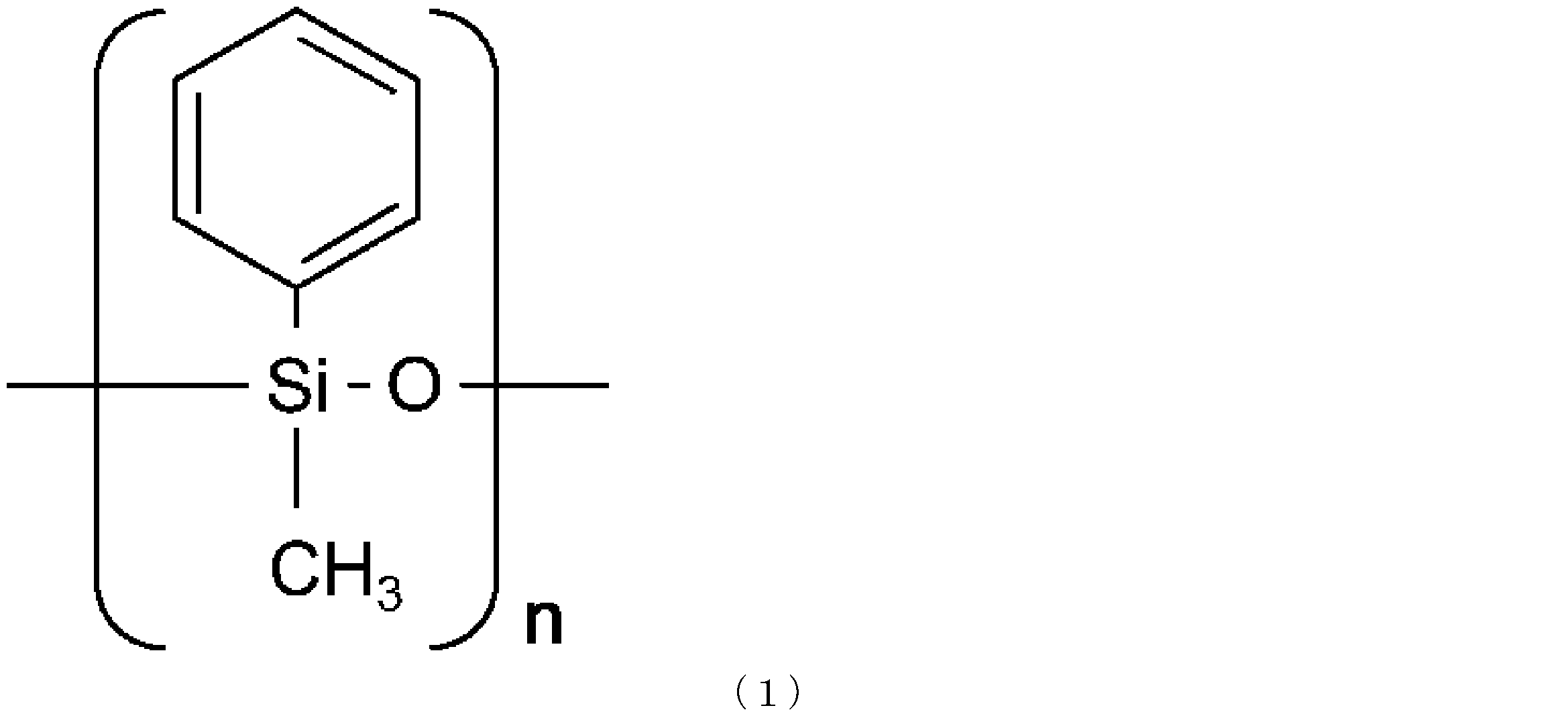
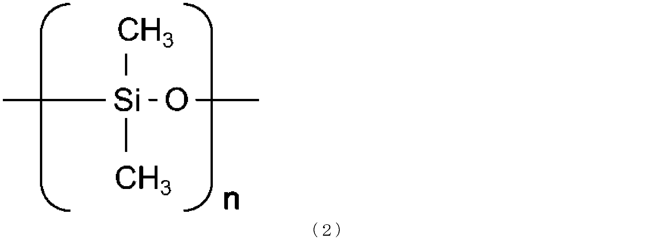

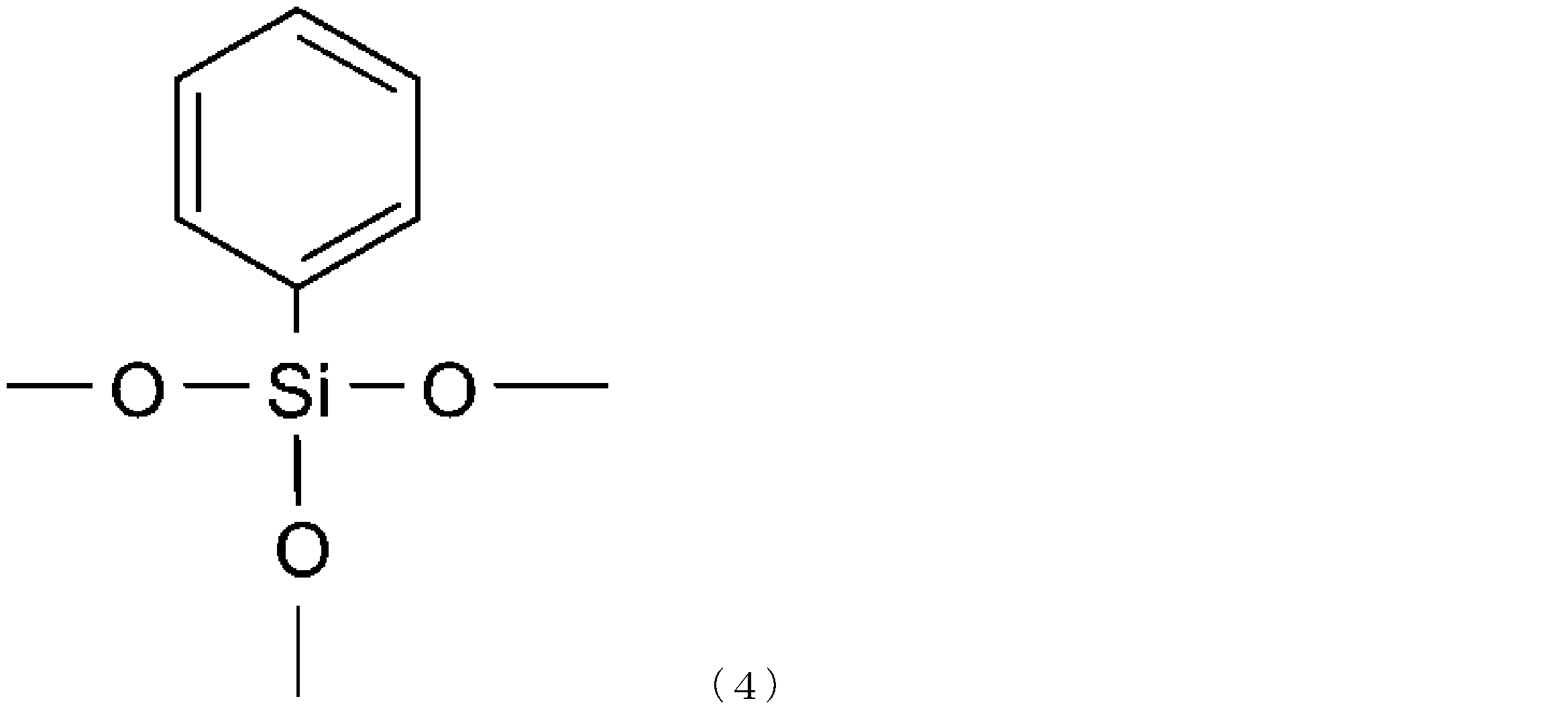
また、上記のシリコーン系樹脂は、接着性を付与できる公知の官能基を有していてもよく、また接着性を付与できる添加物を含有していてもよい。
無機ガラスとしては、Si02、LiO2、及び下記の式(5)を有する材料を用いることができる。これらは単独又は2種以上を混合で用いることができる。

第2の珪酸化合物としては、耐水性、耐候性、耐熱性等の特性や、硬度、伸び等のゴム的性質に優れた硬化物を形成する観点から、例えば、珪素-酸素結合を主骨格としたシロキサン結合からなるシリコーンゴムが好ましい。また、耐熱性の観点から、ジメチルシリコーンゴムがより好ましい。
シリコーンゴムとしては、熱硬化性を有するシリコーンエラストマ、シルセスキオキサン等の珪酸化合物を含有していてもよく、例えば、20℃~200℃、1分間~10時間の加熱処理により硬化して用いることができる。
シリコーンゴムとしては、側鎖や官能基として、メチル基、フェニル基、メチルフェニル基、グリシジル基、イソシアネート基、ビニル基等を有していてもよい。
第一の銀用表面処理剤において、第2の珪酸化合物は、その柔軟性により接着性を得る観点から、線膨張係数が180ppm~450ppmであるものが好ましい。係る範囲内であると、柔軟性による接着性を確保することが容易となるとともに被覆又は封止に用いられる透明封止樹脂により、珪酸化合物に変形が生じることを抑制することができる。柔軟性による接着性を高める観点から、第2の珪酸化合物の線膨張係数は、200ppm~450ppmがより好ましく、被覆又は封止に用いられる透明封止樹脂との接着信頼性を高める観点から、200ppm~350ppmが更に好ましい。珪酸化合物の線膨張係数は、JIS K7197「プラスチックの熱機械分析による線膨張係数試験方法」によるものでTMA(Thermal Mechanical Analysis)に従って測定される値を意味する。
第一の銀用表面処理剤において、第2の珪酸化合物は、絶縁性を確保する観点から、体積抵抗率が1010~1016Ω・cmであるものが好ましい。体積抵抗率の測定における技術的限界及び実用性から、体積抵抗率の上限は、1016Ω・cmでよい。絶縁性を高める観点から、第2の珪酸化合物の体積抵抗率は、1012~1016Ω・cmがより好ましく、1013~1016Ω・cmが更に好ましい。珪酸化合物の体積抵抗率は、珪酸化合物を銅電極付き基板に塗布し、150℃で3時間乾燥させて得られる体積抵抗率測定試験片について、JIS C2139に従って測定される値を意味する。
第2の珪酸化合物の光透過率は、主に照明用に用いられる青色発光ダイオードの中心波長である450nmの光透過率について、1mm厚みに換算した光透過率が、80~100%であることが、光の取出し効率の観点から好ましい。より高輝度の発光ダイオードへの適用性の観点から85~100%がより好ましく、90~100%が更に好ましい。珪酸化合物の光透過率は、PETフィルム上に塗布した珪酸化合物を分光光度計(UV-Vis)により測定して得られる値を意味する。
第一及び第二の銀用表面処理剤において、第2の珪酸化合物の硬化温度は、発光ダイオード素子の耐熱性を考慮して20℃~200℃が好ましく、珪酸化合物の保存安定性の観点から40℃~200℃がより好ましく、生産性の観点から40℃~160℃が更に好ましい。B液からプライマ層を形成する際、成膜性の観点から、上記温度の範囲内で多段加熱してもよい。
また、硬化時間は、1分間~10時間の範囲内で設定することができる。生産性の観点から1分間~8時間の範囲内がより好ましく、プライマ層のレベリング性の観点から3分間~8時間の範囲が更に好ましい。硬化は、プライマ層の上にガスバリア層を設ける前後に分けて実施してもよい。
第一の銀用表面処理剤において、本実施形態に係る第2の珪酸化合物を含有するB液は、溶媒を含有することができる。溶媒は、上記珪酸化合物の溶解性の観点から、脂肪族炭化水素系溶媒、芳香族系溶媒、ケトン系溶媒、エーテル、エステル系溶媒を選択することができる。このような溶媒としては、例えば、ペンタン、ヘキサン、ヘプタン、オクタン、ノナン、デカン等の飽和炭化水素、シクロヘキサン、アルキルシクロヘキサン等の環状炭化水素などを挙げることができる。なお、炭化水素としては、直鎖状、分岐状、環状等、いずれも用いることができる。これらを単独で又は2種以上を混合で用いることができる。
第一の銀用表面処理剤において、本実施形態に係る第2の珪酸化合物を含有するB液の溶媒は、硬化のための加熱工程で蒸発により除去されることが好ましく、沸点が50℃~200℃である溶媒が好ましい。沸点が200℃を超えると乾燥性が低下し、溶媒が残留して接着力を低下させる可能性がある。また、溶媒の沸点が低いと引火の危険性が高まるため、安全性の観点から沸点が50℃以上の溶媒が好ましい。生産性の観点から溶媒の沸点は50℃~160℃が好ましく、硬化のための加熱工程の温度及び時間を自由に選択できる観点から50℃~120℃が更に好ましい。
具体的には、本実施形態に係る銀用表面処理剤のうち、第2の珪酸化合物を含有するB液を銀又は銀合金上に塗布した後、溶媒を除去及び/又は硬化することによって、銀又は銀合金上に第2の珪酸化合物を含んでなる層(プライマ層)を形成できる。さらに、層状珪酸化合物を含有するA液を塗布した後、溶媒を除去することによって層状珪酸化合物を含んでなる層(ガスバリア層)を形成できる。
第二の銀用表面処理剤において、本実施形態において使用される体積抵抗率1010~1016Ω・cmである化合物を含有するB液は、溶媒を含有することができる。溶媒は、上記珪酸化合物の溶解性の観点から、脂肪族炭化水素系溶媒、芳香族系溶媒、ケトン系溶媒、エーテル、エステル系溶媒を選択することができる。このような溶媒としては、例えば、ペンタン、ヘキサン、ヘプタン、オクタン、ノナン、デカン等の飽和炭化水素、シクロヘキサン、アルキルシクロヘキサン等の環状炭化水素などを挙げることができる。なお、炭化水素としては、直鎖状、分岐状、環状等、いずれも用いることができる。これらを単独で又は2種以上を混合で用いることができる。
第二の銀用表面処理剤において、体積抵抗率1010~1016Ω・cmである化合物を含有するB液の溶媒は、硬化のための加熱工程で蒸発により除去されることが好ましく、沸点が50℃~200℃である溶媒が好ましい。沸点が200℃を超えると乾燥性が低下し、溶媒が残留して接着力を低下させる可能性がある。また、溶媒の沸点が低いと引火の危険性が高まるため、安全性の観点から沸点が50℃以上の溶媒が好ましい。生産性の観点から溶媒の沸点は50℃~160℃が好ましく、硬化のための加熱工程の温度及び時間を自由に選択できる観点から50℃~120℃が更に好ましい。
具体的には、本実施形態において使用される銀用表面処理剤のうち、体積抵抗率1010~1016Ω・cmである化合物を含有するB液を銀又は銀合金上に塗布した後、溶媒を除去及び/又は硬化することによって、銀又は銀合金上に体積抵抗率1010~1016Ω・cmである化合物を含んでなる層(プライマ層)を形成できる。さらに、酸素透過率0.0001~10cc/m2・24h・atmである化合物を含有するA液を塗布した後、溶媒を除去することによって酸素透過率0.0001~10cc/m2・24h・atmである化合物を含んでなる層(ガスバリア層)を形成できる。
本実施形態に係る第一及び第二の銀用表面処理剤の塗布方法としては、例えば、バーコート、ディップコート、スピンコート、スプレーコート、ポッティング等の方法を好適に用いることができる。
また、本実施形態に係る第一及び第二の銀用表面処理剤の塗膜から溶媒を除去する方法としては、乾燥を好適に用いることができ、乾燥温度は室温以上であれば特に限定されない。なお、室温とは20~25℃である。
第一の銀用表面処理剤を用いることによって、銀又は銀合金の表面上に、珪酸化合物を含有する層と層状珪酸化合物を含有する層とを有する変色防止膜を形成することができる。かかる膜は、例えば、硫化水素ガスの遮蔽性に優れ、銀硫化防止膜として機能することができる。
第二の銀用表面処理剤を用いることによって、銀又は銀合金の表面上に、体積抵抗率1010~1016Ω・cmである化合物を含有する層と、酸素透過率0.0001~10cc/m2・24h・atmである化合物を含有する層と、を有する変色防止膜を形成することができる。かかる膜は、例えば、硫化水素ガスの遮蔽性に優れ、銀硫化防止膜として機能することができる。
本発明は、上述した本実施形態の第一及び第二の銀用表面処理剤に含有される固体成分からなる膜を具備する銀又は銀合金を提供することができる。また、かかる銀又は銀合金を有する基板と、発光ダイオードとを具備する発光装置を提供することができる。かかる発光装置は、透明樹脂で封止されていてもよい。透明樹脂としては、シリコーン樹脂等が挙げられる。また、銀又は銀合金を有する基板は、表面に凹凸形状を有することができ、銀又は銀合金が凹凸形状を有していてもよい。
次に、第11及び第12の実施形態に係る発光装置の製造方法について説明する。共通する点はまとめて説明し、相違する点はそれぞれ説明する。
図28は、第11及び第12の実施形態に係る発光装置の製造方法を示したフローチャートである。図28に示すように、発光装置の製造方法では、まず、基板準備工程(ステップS101)として、表面に銅めっき板214が配線された絶縁性の基体212を準備し、銀めっき層形成工程(ステップS102)として、銅めっき板214の表面に銀めっき層216を形成する。
次に、リフレクタ形成工程(ステップS103)として、基板210の表面にリフレクタ220を形成し、チップ搭載工程(ステップS104)として、基板210に青色LED230を搭載する。青色LED230の基板210への搭載は、リフレクタ220で囲まれた内側空間222において、アノード側及びカソード側の何れか一方の銀めっき層216に青色LED230をダイボンディングすることにより行う。これにより、青色LED230がダイボンド材232を介してアノード側及びカソード側の何れか一方の銀めっき層216と導通されるとともに、青色LED230がリフレクタ220に取り囲まれて内側空間222に収容された状態となる。
次に、第11の実施形態に係る発光装置を製造する場合は、B液の塗布工程(ステップS105)として、銀めっき層216に本実施形態の銀用表面処理剤のうち、第2の珪酸化合物を含有するB液を塗布して銀めっき層216をB液で覆う。
第12の実施形態に係る発光装置を製造する場合は、B液の塗布工程(ステップS105)として、銀めっき層216に銀用表面処理剤のうち、体積抵抗率1010~1016Ω・cmである化合物を含有するB液を塗布して銀めっき層216をB液で覆う。
B液の塗布工程(ステップS105)におけるB液の塗布は、例えば、基板210の表面側から、銀用表面処理剤を内側空間222に滴下又は散布することにより行う。このとき、少なくとも銀めっき層216の全てがB液Mで覆われるように、B液の滴下量又は散布量を調節する。この場合、例えば、図29の(a)に示すように、銀めっき層216及び青色LED230の全てがB液Mで覆われるように、B液Mを内側空間222に滴下又は散布してもよく、図29の(b)に示すように、銀めっき層216及び青色LED230の全てとリフレクタ220の内周面220aの一部とがB液Mで覆われるように、B液Mを内側空間222に滴下又は散布してもよく、図29の(c)に示すように、銀めっき層216、青色LED230及びリフレクタ220の内周面220aの全てがB液Mで覆われるように、B液Mを内側空間222に滴下又は散布してもよい。
次に、乾燥工程(ステップS106)として、銀めっき層216に塗布した銀用表面処理剤のうち、B液の塗膜を乾燥させて銀硫化防止膜のうち、第2の珪酸化合物を含有する層(プライマ層250)を形成する。
次に、第11の実施形態に係る発光装置を製造する場合は、A液の塗布工程(ステップS107)として、プライマ層250上に、本実施形態の銀用表面処理剤のうち、層状珪酸化合物を含有するA液を塗布して、プライマ層250のうちの少なくとも銀めっき層216を被覆している部分をA液で覆う。
第12の実施形態に係る発光装置を製造する場合は、A液の塗布工程(ステップS107)として、プライマ層250上に、銀用表面処理剤のうち、酸素透過率0.0001~10cc/m2・24h・atmである化合物を含有するA液を塗布して、プライマ層250のうちの少なくとも銀めっき層216を被覆している部分をA液で覆う。
A液の塗布工程(ステップS107)におけるA液の塗布は、例えば、基板210の表面側から、銀用表面処理剤を内側空間222に滴下又は散布することにより行う。滴下又は散布の方法は、ステップS105のB液の塗布工程と同様にして行うことができる。
次に、第11の実施形態に係る発光装置を製造する場合は、乾燥工程(ステップS108)として、銀めっき層216に塗布したA液の塗膜を乾燥させて変色防止膜260のうち、層状珪酸化合物を含有する層(ガスバリア層252)を形成する。
第12の実施形態に係る発光装置を製造する場合は、乾燥工程(ステップS108)として、銀めっき層216に塗布したA液の塗膜を乾燥させて変色防止膜260のうち、酸素透過率0.0001~10cc/m2・24h・atmである化合物を含有する層(ガスバリア層252)を形成する。
乾燥工程(ステップS106及びS108)は、溶媒が揮発する温度で行うことができ、例えば、30℃以上80℃以下の温度範囲とすることが好ましく、30℃以上70℃以下の温度範囲とすることがより好ましく、30℃以上60℃以下の温度範囲とすることがさらにより好ましい。この温度域を保つ時間は、例えば、5分以上とすることができ、十分に乾燥させるという点で、5分以上1日以下とすることが好ましく、生産性を向上させる観点から、5分以上30分以下とすることがより好ましい。
このようにして乾燥工程を行うことで、図29の(a)に示したB液Mは、図30の(a)に示すように、銀めっき層216及び青色LED230の全てを被覆するプライマ層250となり、図29の(b)に示したB液Mは、図30の(b)に示すように、銀めっき層216及び青色LED230の全てとリフレクタ220の内周面220aの一部とを被覆するプライマ層250となり、図29の(c)に示したB液Mは、図30の(c)に示すように、銀めっき層216、青色LED230及びリフレクタ220の内周面220aの全てを被覆するプライマ層250となる。A液の乾燥により形成されるガスバリア層252についても、同様である。ガスバリア層252が被覆する面積は、プライマ層250の被覆する面積よりも小さいことが好ましい。
本実施形態においては上記の乾燥工程の後に150℃、30分間の条件で2層からなる変色防止膜260を十分に乾燥することが好ましい。これにより、プライマ層250とガスバリア層252の層間を狭めることによる変色防止性の更なる向上の効果を得ることができる。
次に、ワイヤボンディング工程(ステップS109)として、青色LED230とアノード側及びカソード側の何れか他方の銀めっき層216とをワイヤボンディングする。このとき、銀めっき層216は変色防止膜260で被覆されているため、青色LED230及び銀めっき層216に被覆されている変色防止膜260を突き破るようにワイヤの両端を青色LED230と銀めっき層216とにボンディングすることで、青色LED230と銀めっき層216とを導通させる。なお、変色防止膜260の突き破りは、例えば、変色防止膜260の層厚を調節することや、ワイヤボンディングを行うボンディングヘッドの荷重を調節することや、このボンディングヘッドを振動させることなどにより行うことができる。
次に、透明封止樹脂充填工程(ステップS110)として、リフレクタ220の内周面220aにより形成される内側空間222に、蛍光体242が含有された透明封止樹脂240を充填する。これにより、青色LED230及び銀めっき層216が透明封止樹脂240(透明封止部)により封止される。
このようにして透明封止樹脂充填工程を行うことで、図31の(a)に示すように、銀めっき層216及び青色LED230の全てが2層からなる変色防止膜260(プライマ層250及びガスバリア層252)で被覆された状態で、銀めっき層216及び青色LED230が透明封止樹脂240により封止された発光装置201、図31の(b)に示すように、銀めっき層216及び青色LED230の全てとリフレクタ220の内周面220aの一部とが変色防止膜260で被覆された状態で、銀めっき層216及び青色LED230が透明封止樹脂240により封止された発光装置201、又は、図31の(c)に示すように、銀めっき層216、青色LED230及びリフレクタ220の内周面220aの全てが変色防止膜260で被覆された状態で、銀めっき層216及び青色LED230が透明封止樹脂240により封止された発光装置201を得ることができる。
このように、第11の実施形態に係る発光装置を発光装置201として製造する場合、本実施形態の第一の銀用表面処理剤(A液及びB液)で銀めっき層216を覆ったのち、銀用表面処理剤の塗膜を乾燥させることで、銀用表面処理剤に含まれる層状珪酸化合物が積層したガスバリア層を備える変色防止膜260が形成され、銀めっき層216が変色防止膜260で被覆される。これにより、銀めっき層216を適切に被覆できる2層からなる変色防止膜260を形成することができる。
第12の実施形態に係る発光装置を発光装置201として製造する場合、本実施形態の第二の銀用表面処理剤(A液及びB液)で銀めっき層216を覆ったのち、銀用表面処理剤の塗膜を乾燥させることで、銀用表面処理剤に含まれる酸素透過率0.0001~10cc/m2・24h・atmである化合物が積層したガスバリア層を備える変色防止膜260が形成され、銀めっき層216が変色防止膜260で被覆される。これにより、銀めっき層216を適切に被覆できる2層からなる変色防止膜260を形成することができる。
発光装置201に設けられたリフレクタ220の内側空間222に本実施形態の銀用表面処理剤を滴下又は散布することで、容易に銀めっき層を覆う変色防止膜260を形成することができる。
[第13及び第14の実施形態]
次に、発光装置の製造方法の第13及び第14の実施形態について説明する。第13及び第14の実施形態に係る発光装置の製造方法は、基本的に第11及び第12の実施形態に係る発光装置の製造方法と同様であるが、工程の順序のみ第11及び第12の実施形態に係る発光装置の製造方法と相違する。このため、以下の説明では、第11及び第12の実施形態に係る発光装置の製造方法と相違する部分のみを説明し、第11及び第12の実施形態に係る発光装置の製造方法と同様の部分の説明を省略する。なお、銀用表面処理剤は、上述したものを用いることができる。
次に、発光装置の製造方法の第13及び第14の実施形態について説明する。第13及び第14の実施形態に係る発光装置の製造方法は、基本的に第11及び第12の実施形態に係る発光装置の製造方法と同様であるが、工程の順序のみ第11及び第12の実施形態に係る発光装置の製造方法と相違する。このため、以下の説明では、第11及び第12の実施形態に係る発光装置の製造方法と相違する部分のみを説明し、第11及び第12の実施形態に係る発光装置の製造方法と同様の部分の説明を省略する。なお、銀用表面処理剤は、上述したものを用いることができる。
図33は、第13及び第14の実施形態における発光装置の製造方法を示したフローチャートである。図34は、図33の製造方法により製造した発光装置の断面図である。
図33に示すように、第13及び第14の実施形態に係る発光装置201の製造方法は、まず、第11及び第12の実施形態と同様に、基板準備工程(ステップS201)、銀めっき層形成工程(ステップS202)及びリフレクタ形成工程(ステップS203)をこの順序で行う。なお、基板準備工程(ステップS201)、銀めっき層形成工程(ステップS202)及びリフレクタ形成工程(ステップS203)は、第11の実施形態の基板準備工程(ステップS101)、銀めっき層形成工程(ステップS102)及びリフレクタ形成工程(ステップS103)と同様である。
次に、B液の塗布工程(ステップS204)として、銀めっき層216にB液を塗布して銀めっき層216をB液で覆う。なお、塗布工程(ステップS204)は、第11及び第12の実施形態の塗布工程(ステップS105)と同様に行うことができる。
次に、乾燥工程(ステップS205)として、銀めっき層216に塗布したB液の塗膜を乾燥させてプライマ層250を形成する。なお、乾燥工程(ステップS205)は、第11及び第12の実施形態の乾燥工程(ステップS106)と同様に行うことができる。
次に、A液の塗布工程(ステップS206)として、プライマ層250上にA液を塗布してプライマ層250の少なくとも銀めっき層216を被覆する部分をA液で覆う。なお、塗布工程(ステップS206)は、第11及び第12の実施形態の塗布工程(ステップS105)と同様に行うことができる。
次に、乾燥工程(ステップS207)として、銀めっき層216に塗布したA液の塗膜を乾燥させてガスバリア層252を形成する。なお、乾燥工程(ステップS207)は、第11及び第12の実施形態の乾燥工程(ステップS106)と同様に行うことができる。
次に、チップ搭載工程(ステップS208)として、アノード側及びカソード側の何れか一方の銀めっき層216に青色LED230をダイボンディングする。このとき、第11及び第12の実施形態のワイヤボンディング工程(ステップS109)と同様に、銀めっき層216に被覆されている変色防止膜を突き破るように青色LED230を銀めっき層216にボンディングすることで、青色LED230と銀めっき層216とを導通させる。
次に、ワイヤボンディング工程(ステップS209)として、青色LED230とアノード側及びカソード側の何れか他方の銀めっき層216とをワイヤボンディングする。このとき、銀めっき層216は変色防止膜260で被覆されているため、第11及び第12の実施形態のワイヤボンディング工程(ステップS109)と同様に、銀めっき層216に被覆されている2層からなる変色防止膜260を突き破るようにワイヤの一端を銀めっき層216にボンディングする。一方、青色LED230は変色防止膜260で被覆されていないため、ボンディングワイヤ234の他端は、通常通り、青色LED230にボンディングすることができる。これにより、青色LED230と銀めっき層216とが導通される。
次に、ステップS210として透明封止樹脂充填工程を行う。
このように、第13及び第14の実施形態に係る発光装置の製造方法によれば、銀用表面処理剤の塗布工程及び乾燥工程を経てからチップ搭載工程を行うことで、図34に示すように、青色LED230が2層からなる変色防止膜260で被覆されない発光装置201を製造することができる。これにより、ワイヤボンディング工程において、ボンディングワイヤ234の一端を青色LED230にボンディングする際に、第11及び第12の実施形態に係る発光装置の製造方法のように、2層からなる変色防止膜260を突き破る必要がなくなる。
[第15及び第16の実施形態]
次に、発光装置の製造方法の第15及び第16の実施形態について説明する。第15及び第16の実施形態に係る発光装置の製造方法は、基本的に第11及び第12の実施形態に係る発光装置の製造方法と同様であるが、工程の順序のみ第第11及び第12の実施形態に係る発光装置の製造方法と相違する。このため、以下の説明では、第11及び第12の実施形態に係る発光装置の製造方法と相違する部分のみを説明し、第11及び第12の実施形態に係る発光装置の製造方法と同様の部分の説明を省略する。なお、銀用表面処理剤は、上述したものを用いることができる。
次に、発光装置の製造方法の第15及び第16の実施形態について説明する。第15及び第16の実施形態に係る発光装置の製造方法は、基本的に第11及び第12の実施形態に係る発光装置の製造方法と同様であるが、工程の順序のみ第第11及び第12の実施形態に係る発光装置の製造方法と相違する。このため、以下の説明では、第11及び第12の実施形態に係る発光装置の製造方法と相違する部分のみを説明し、第11及び第12の実施形態に係る発光装置の製造方法と同様の部分の説明を省略する。なお、銀用表面処理剤は、上述したものを用いることができる。
図35は、第15及び第16の実施形態における発光装置の製造方法を示したフローチャートである。図36は、図35の製造方法により製造した発光装置の断面図である。
図35に示すように、第15及び第16の実施形態に係る発光装置201の製造方法は、まず、第11及び第12の実施形態と同様に、基板準備工程(ステップS301)及び銀めっき層形成工程(ステップS302)をこの順序で行う。なお、基板準備工程(ステップS301)及び銀めっき層形成工程(ステップS302)は、第11及び第12の実施形態の基板準備工程(ステップS101)及び銀めっき層形成工程(ステップS102)と同様である。
次に、B液の塗布工程(ステップS303)として、銀めっき層216にB液を塗布して銀めっき層216をB液で覆う。このとき、作業性の観点から、B液を銀めっき層216が形成されている基板210の表面全体に塗布することが好ましいが、銀めっき層216のみを覆うようにB液を塗布してもよい。
次に、乾燥工程(ステップS304)として、銀めっき層216に塗布したB液の塗膜を乾燥させてプライマ層250を形成する。なお、乾燥工程(ステップS304)は、第11及び第12の実施形態の乾燥工程(ステップS106)と同様に行うことができる。
次に、A液の塗布工程(ステップS305)として、プライマ層250上にA液を塗布してプライマ層250の少なくとも銀めっき層216を被覆する部分をA液で覆う。このとき、作業性の観点から、A液をプライマ層250全体に塗布することが好ましいが、プライマ層250の銀めっき層216を被覆する部分のみを覆うようにA液を塗布してもよい。
次に、乾燥工程(ステップS306)として、プライマ層250上に塗布したA液の塗膜を乾燥させてガスバリア層252を形成する。なお、乾燥工程(ステップS306)は、第11及び第12の実施形態の乾燥工程(ステップS106)と同様に行うことができる。
次に、リフレクタ形成工程(ステップS307)として、基板210の表面にリフレクタ220を形成する。このとき、銀用表面処理剤(B液及びA液)の塗布工程(ステップS303及びS305)で基板210の表面全体に銀用表面処理剤を塗布した場合は、基板210の表面を被覆している2層からなる変色防止膜260の表面にリフレクタ220を形成する。
次に、チップ搭載工程(ステップS308)として、アノード側及びカソード側の何れか一方の銀めっき層216に青色LED230をダイボンディングする。このとき、第11及び第12の実施形態のワイヤボンディング工程(ステップS109)と同様に、銀めっき層216に被覆されている2層からなる変色防止膜260を突き破るように青色LED230を銀めっき層216にボンディングすることで、青色LED230と銀めっき層216とを導通させる。
次に、ワイヤボンディング工程(ステップS309)として、青色LED230とアノード側及びカソード側の何れか他方の銀めっき層216とをワイヤボンディングする。このとき、銀めっき層216は変色防止膜260で被覆されているため、第11及び第12の実施形態のワイヤボンディング工程(ステップS109)と同様に、銀めっき層216に被覆されている2層からなる変色防止膜260を突き破るようにワイヤの一端を銀めっき層216にボンディングする。一方、青色LED230は変色防止膜260で被覆されていないため、ボンディングワイヤ234の他端は、通常通り青色LED230にボンディングすることができる。これにより、青色LED230と銀めっき層216とが導通される。
次に、ステップS310として透明封止樹脂充填工程を行う。
このように、第15及び第16の実施形態に係る発光装置の製造方法によれば、銀用表面処理剤の塗布工程及び乾燥工程を経てからリフレクタ形成工程及びチップ搭載工程を行うことで、図36に示すように、青色LED230が2層からなる変色防止膜260で被覆されない発光装置201を製造することができる。これにより、ワイヤボンディング工程において、ボンディングワイヤ234の一端を青色LED230にボンディングする際に、第11及び第12の実施形態に係る発光装置の製造方法のように、2層からなる変色防止膜260を突き破る必要がなくなる。
以上、本発明の好適な実施形態について説明したが、本発明は上記実施形態に限定されるものではない。
上記実施形態では、発光装置201にボンディングする発光ダイオードとして、青色の光を発生する青色LED230を採用するものとして説明したが、青色以外の光を発生する発光ダイオードを採用するものとしてもよい。
また、上記実施形態の発光装置201は、青色LED230を取り囲むリフレクタ220を備えるものとして説明したが、このようなリフレクタ220を備えないものとしてもよい。
本実施形態の銀用表面処理剤によれば、銀の変色防止性に優れた変色防止膜、特には銀の硫化防止性に優れた銀硫化防止膜を形成できることから、蛍光体として従来から使用されている、Y2O2S:Eu(赤)、ZnS:Cu(緑)、ZnS:Ag(青)、特開平8-085787号公報に示される化合物等の硫黄含有化合物が用いられた発光装置であっても十分な耐硫化性を得ることができる。
本実施形態の銀用表面処理剤は、上述した発光装置以外に、例えば、銀を含有する反射防止膜を備えるプラズマディスプレイ、液晶ディスプレイ等にも適用することができる。
以下、実施例及び比較例によって、本発明をさらに具体的に説明するが、本発明は以下の実施例に限定されるものではない。
(実施例A1)
層状珪酸化合物として、平均長辺長さ10000nmのマイカ水分散液(コープケミカル株式会社製、MEB-3)を用意した。このマイカ水分散液12.5gに蒸留水を添加して全質量100gとした後、自転・公転ミキサー(株式会社シンキー製、ARE-310)を用いて2000rpmで、10分間、混合を行い、2200rpmで、10分間、脱泡を行い、平均長辺長さ10000nmのマイカを1質量%含む表面処理剤Aを得た。
層状珪酸化合物として、平均長辺長さ10000nmのマイカ水分散液(コープケミカル株式会社製、MEB-3)を用意した。このマイカ水分散液12.5gに蒸留水を添加して全質量100gとした後、自転・公転ミキサー(株式会社シンキー製、ARE-310)を用いて2000rpmで、10分間、混合を行い、2200rpmで、10分間、脱泡を行い、平均長辺長さ10000nmのマイカを1質量%含む表面処理剤Aを得た。
層状珪酸化合物の平均長辺長さは、透過型電子顕微鏡(日本電子製、JEM-2100F)を用い、縦100μm×横100μmの範囲の画像内における全ての粒子の長辺長さの値を平均化して求めた。なお、各粒子の長辺長さは、粒子の外接長方形の長辺の長さが最大となるときの当該長辺の長さとした。
第2の珪酸化合物として、ダウコーニング製シリコーン樹脂(OE-6370M)1gにノルマルヘプタン99gを添加し、全重量を100gとして、第2の珪酸化合物を1質量%含む表面処理剤Bを調製した。
<評価用銀基板の作製>
ソーダガラス製のスライドガラスに厚さ100nmの銀を蒸着した銀基板上に、wet厚12μmのバーコーターを用いて、上記で得られた第2の珪酸化合物1質量%含む表面処理剤Bを塗布後、22℃で30分間静置して溶媒を除去し、150℃1時間の加熱処理をした。そして、上記で得られた層状珪酸化合物を1質量%含む表面処理剤Aを塗布し、22℃で12時間静置して溶媒を除去し、プライマ層、及びガスバリア層(マイカ膜)を表面に具備する銀基板(評価用銀基板)を得た。なお、wet厚とは、溶媒を除去する前の表面処理剤の塗布直後の厚みである。
ソーダガラス製のスライドガラスに厚さ100nmの銀を蒸着した銀基板上に、wet厚12μmのバーコーターを用いて、上記で得られた第2の珪酸化合物1質量%含む表面処理剤Bを塗布後、22℃で30分間静置して溶媒を除去し、150℃1時間の加熱処理をした。そして、上記で得られた層状珪酸化合物を1質量%含む表面処理剤Aを塗布し、22℃で12時間静置して溶媒を除去し、プライマ層、及びガスバリア層(マイカ膜)を表面に具備する銀基板(評価用銀基板)を得た。なお、wet厚とは、溶媒を除去する前の表面処理剤の塗布直後の厚みである。
<評価用発光装置の作製>
エノモト株式会社製の3528サイズのLED用リードフレーム(OP4)に、発光波長467.5nm~470nm、容量3.7μLの発光ダイオードチップを金ワイヤで接続し、発光装置を作製した。その後、発光ダイオード上に上記で得られた第2の珪酸化合物を1質量%含む表面処理剤B(第2の珪酸化合物層形成材料)をスポイトで0.03mL滴下し、22℃で30分間静置して溶媒を除去し、150℃1時間の加熱処理をした。その後、表面処理剤Aをスポイトで0.03mL滴下し、22℃で12時間静置して溶媒を除去し、銀メッキ基板上にプライマ層及びガスバリア層を具備する発光装置を得た。その後、150℃1時間の加熱処理をした後、ダウコーニング製透明シリコーン封止材(OE-6631)を用いて封止し、150℃5時間の熱処理により、硬化することで評価用発光装置を得た。図37は、実施例において銀用表面処理剤を用いて形成した銀硫化変色防止膜の一例について撮影した材の断面TEM写真である。
エノモト株式会社製の3528サイズのLED用リードフレーム(OP4)に、発光波長467.5nm~470nm、容量3.7μLの発光ダイオードチップを金ワイヤで接続し、発光装置を作製した。その後、発光ダイオード上に上記で得られた第2の珪酸化合物を1質量%含む表面処理剤B(第2の珪酸化合物層形成材料)をスポイトで0.03mL滴下し、22℃で30分間静置して溶媒を除去し、150℃1時間の加熱処理をした。その後、表面処理剤Aをスポイトで0.03mL滴下し、22℃で12時間静置して溶媒を除去し、銀メッキ基板上にプライマ層及びガスバリア層を具備する発光装置を得た。その後、150℃1時間の加熱処理をした後、ダウコーニング製透明シリコーン封止材(OE-6631)を用いて封止し、150℃5時間の熱処理により、硬化することで評価用発光装置を得た。図37は、実施例において銀用表面処理剤を用いて形成した銀硫化変色防止膜の一例について撮影した材の断面TEM写真である。
<表面処理剤を塗布した銀基板の硫化水素ガス耐性評価>
まず、上記で得られた評価用銀基板の波長550nmの可視光反射率を、分光光度計(日本分光、V-570)を用いて測定し、[硫化水素暴露前反射率]とした。次に、評価用銀基板を、10ppm硫化水素ガス気流、40℃、90%RH(相対湿度)中に96時間静置した後、波長550nmの可視光反射率を測定し、[硫化水素暴露後反射率]とした。
[硫化水素暴露前反射率]-[硫化水素暴露後反射率]=[反射低下率]とし、反射低下率を求めた。結果を表1に示す。
まず、上記で得られた評価用銀基板の波長550nmの可視光反射率を、分光光度計(日本分光、V-570)を用いて測定し、[硫化水素暴露前反射率]とした。次に、評価用銀基板を、10ppm硫化水素ガス気流、40℃、90%RH(相対湿度)中に96時間静置した後、波長550nmの可視光反射率を測定し、[硫化水素暴露後反射率]とした。
[硫化水素暴露前反射率]-[硫化水素暴露後反射率]=[反射低下率]とし、反射低下率を求めた。結果を表1に示す。
<表面処理剤を塗布した発光装置の硫化水素ガス耐性評価>
評価用発光装置を順電流20mA、順電圧3.3Vで発光させ、マルチ測光計(大塚電子株式会社、MCPD-3700)を用いて露光時間30ミリ秒で発光強度を測定し、[硫化水素暴露前発光強度]とした。次に、評価用発光装置を、10ppm硫化水素ガス気流、40℃、90%RH(相対湿度)中に96時間静置した後、順電流20mA、順電圧3.3Vで発光させ、マルチ測光計を用いて露光時間30ミリ秒で発光強度を測定し、[硫化水素暴露後発光強度]とした。
([硫化水素暴露後発光強度]/[硫化水素暴露前発光強度])×100=[発光強度維持率]とし、発光強度維持率を求めた。結果を表1に示す。
評価用発光装置を順電流20mA、順電圧3.3Vで発光させ、マルチ測光計(大塚電子株式会社、MCPD-3700)を用いて露光時間30ミリ秒で発光強度を測定し、[硫化水素暴露前発光強度]とした。次に、評価用発光装置を、10ppm硫化水素ガス気流、40℃、90%RH(相対湿度)中に96時間静置した後、順電流20mA、順電圧3.3Vで発光させ、マルチ測光計を用いて露光時間30ミリ秒で発光強度を測定し、[硫化水素暴露後発光強度]とした。
([硫化水素暴露後発光強度]/[硫化水素暴露前発光強度])×100=[発光強度維持率]とし、発光強度維持率を求めた。結果を表1に示す。
<表面処理剤を塗布した発光装置の絶縁信頼性評価>
評価用発光装置を順電流20mA、順電圧3.3Vで発光させ、マルチ測光計(大塚電子株式会社、MCPD-3700)を用いて露光時間30ミリ秒で発光強度を測定し、[試験前発光強度]とした。評価用発光装置を順電流20mA、順電圧3.3Vで発光させながら、85℃、85%RH(相対湿度)中に50時間静置した後、目視観察した。また、順電流20mA、順電圧3.3Vで発光させ、マルチ測光計(大塚電子株式会社、MCPD-3700)を用いて露光時間30ミリ秒で発光強度を測定し、[試験後発光強度]とした。目視観察により、電気化学的マイグレーションの発生による電極間の変色があり、([試験後発光強度]/[試験前発光強度])×100=[発光強度維持率]として求めた。電極間の変色が確認され、発光強度維持率が97%以下の場合を不良として×と評価し、電極間の変色が全く無く、発光強度維持率が100%の場合を良好として○と評価した。目視観察により、電極間に多少の変色が認められるものの発光強度維持率が97%を超える場合を許容として△と評価した。結果を表1に示す。
評価用発光装置を順電流20mA、順電圧3.3Vで発光させ、マルチ測光計(大塚電子株式会社、MCPD-3700)を用いて露光時間30ミリ秒で発光強度を測定し、[試験前発光強度]とした。評価用発光装置を順電流20mA、順電圧3.3Vで発光させながら、85℃、85%RH(相対湿度)中に50時間静置した後、目視観察した。また、順電流20mA、順電圧3.3Vで発光させ、マルチ測光計(大塚電子株式会社、MCPD-3700)を用いて露光時間30ミリ秒で発光強度を測定し、[試験後発光強度]とした。目視観察により、電気化学的マイグレーションの発生による電極間の変色があり、([試験後発光強度]/[試験前発光強度])×100=[発光強度維持率]として求めた。電極間の変色が確認され、発光強度維持率が97%以下の場合を不良として×と評価し、電極間の変色が全く無く、発光強度維持率が100%の場合を良好として○と評価した。目視観察により、電極間に多少の変色が認められるものの発光強度維持率が97%を超える場合を許容として△と評価した。結果を表1に示す。
<表面処理剤を塗布した発光装置の接着性評価:レッドインク試験>
評価用発光装置を、万年筆用ボトルインク赤(PILOT社製、INK30R)に25℃で24時間浸漬した後、取り出して水洗した。実体顕微鏡を用いて、インクによる着色の有無を観察し、インクの染込みによる赤色の着色が無い場合を接着性良好として○、ある場合を接着性不良として×と判定した。結果を表1に示す。
評価用発光装置を、万年筆用ボトルインク赤(PILOT社製、INK30R)に25℃で24時間浸漬した後、取り出して水洗した。実体顕微鏡を用いて、インクによる着色の有無を観察し、インクの染込みによる赤色の着色が無い場合を接着性良好として○、ある場合を接着性不良として×と判定した。結果を表1に示す。
<剥離試験用発光装置の作製>
エノモト株式会社製の3528サイズのLED用リードフレーム(OP4)に、発光波長467.5nm~470nm、容量3.7μLの発光ダイオードチップを金ワイヤで接続し、発光装置を作製した。その後、発光ダイオード上に上記で得られた第2の珪酸化合物を1質量%含む表面処理剤B(第2の珪酸化合物層形成材料)をスポイトで0.03mL滴下し、22℃で30分間静置して溶媒を除去し、150℃1時間の加熱処理をした。その後、表面処理剤Aをスポイトで0.03mL滴下し、22℃で12時間静置して溶媒を除去し、銀メッキ基板上にプライマ層及びガスバリア層を具備する発光装置を得た。その後、150℃1時間の加熱処理をした後、ダウコーニング製透明シリコーン封止材(OE-6631)を用いて封止し、Quad Group社製φ1.8mm銅製スタッドピン(901070U)のスタッド側を封止材の中に垂直に立て、150℃5時間の熱処理により、硬化することで剥離試験用発光装置を得た。
エノモト株式会社製の3528サイズのLED用リードフレーム(OP4)に、発光波長467.5nm~470nm、容量3.7μLの発光ダイオードチップを金ワイヤで接続し、発光装置を作製した。その後、発光ダイオード上に上記で得られた第2の珪酸化合物を1質量%含む表面処理剤B(第2の珪酸化合物層形成材料)をスポイトで0.03mL滴下し、22℃で30分間静置して溶媒を除去し、150℃1時間の加熱処理をした。その後、表面処理剤Aをスポイトで0.03mL滴下し、22℃で12時間静置して溶媒を除去し、銀メッキ基板上にプライマ層及びガスバリア層を具備する発光装置を得た。その後、150℃1時間の加熱処理をした後、ダウコーニング製透明シリコーン封止材(OE-6631)を用いて封止し、Quad Group社製φ1.8mm銅製スタッドピン(901070U)のスタッド側を封止材の中に垂直に立て、150℃5時間の熱処理により、硬化することで剥離試験用発光装置を得た。
<表面処理剤を塗布した発光装置の剥離試験>
剥離試験用発光装置を、ロミュラス製スタッドピンプル試験機にセットし、1.5N/秒の速度で剥離し、剥離力を測定した。結果を表1に示す。
剥離試験用発光装置を、ロミュラス製スタッドピンプル試験機にセットし、1.5N/秒の速度で剥離し、剥離力を測定した。結果を表1に示す。
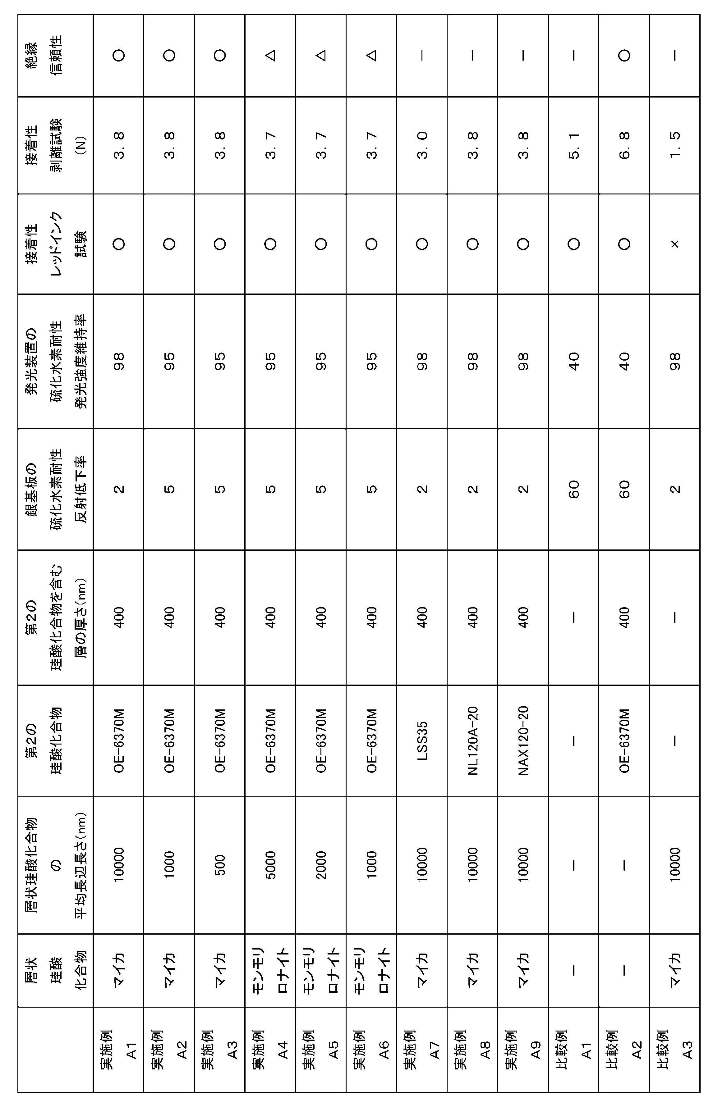
(実施例A2)
平均長辺長さ1000nmのマイカ(トピー工業株式会社製、NTS-5)を使用し、このマイカ1gに蒸留水を添加して全重量100gとした以外は実施例A1と同様にして表面処理剤を作製し、実施例A1と同様に評価を行った。
平均長辺長さ1000nmのマイカ(トピー工業株式会社製、NTS-5)を使用し、このマイカ1gに蒸留水を添加して全重量100gとした以外は実施例A1と同様にして表面処理剤を作製し、実施例A1と同様に評価を行った。
(実施例A3)
平均長辺長さ500nmのマイカ(トピー工業株式会社製、NHT-B2)を使用し、このマイカ1gに蒸留水を添加して全重量100gとした以外は実施例A1と同様にして表面処理剤を作製し、実施例A1と同様に評価を行った。
平均長辺長さ500nmのマイカ(トピー工業株式会社製、NHT-B2)を使用し、このマイカ1gに蒸留水を添加して全重量100gとした以外は実施例A1と同様にして表面処理剤を作製し、実施例A1と同様に評価を行った。
(実施例A4)
平均長辺長さ5000nmのモンモリロナイト(クニミネ工業株式会社製、クニピアF)を使用し、このモンモリロナイト1gに蒸留水を添加して全重量100gとした以外は実施例A1と同様にして表面処理剤を作製し、実施例A1と同様に評価を行った。
平均長辺長さ5000nmのモンモリロナイト(クニミネ工業株式会社製、クニピアF)を使用し、このモンモリロナイト1gに蒸留水を添加して全重量100gとした以外は実施例A1と同様にして表面処理剤を作製し、実施例A1と同様に評価を行った。
(実施例A5)
平均長辺長さ2000nmのモンモリロナイト(クニミネ工業株式会社製、クニピアF)を使用し、このモンモリロナイト1gに蒸留水を添加して全重量100gとした以外は実施例A1と同様にして表面処理剤を作製し、実施例A1と同様に評価を行った。
平均長辺長さ2000nmのモンモリロナイト(クニミネ工業株式会社製、クニピアF)を使用し、このモンモリロナイト1gに蒸留水を添加して全重量100gとした以外は実施例A1と同様にして表面処理剤を作製し、実施例A1と同様に評価を行った。
(実施例A6)
平均長辺長さ1000nmのモンモリロナイト(クニミネ工業株式会社製、クニピアF)を使用し、このモンモリロナイト1gに蒸留水を添加して全重量100gとした以外は実施例A1と同様にして表面処理剤を作製し、実施例A1と同様に評価を行った。
平均長辺長さ1000nmのモンモリロナイト(クニミネ工業株式会社製、クニピアF)を使用し、このモンモリロナイト1gに蒸留水を添加して全重量100gとした以外は実施例A1と同様にして表面処理剤を作製し、実施例A1と同様に評価を行った。
(実施例A7)
第2の珪酸化合物としてリチウムシリケート(日産化学株式会社製、LSS35)0.01gを使用した以外は実施例A1と同様にして表面処理剤を作製し、実施例A1と同様に評価を行った。
第2の珪酸化合物としてリチウムシリケート(日産化学株式会社製、LSS35)0.01gを使用した以外は実施例A1と同様にして表面処理剤を作製し、実施例A1と同様に評価を行った。
(実施例A8)
第2の珪酸化合物としてポリシラザン20%溶液(AZ Electronic Materials製、NL120A-20)1gを脱水ジブチルエーテル39gに溶解したものを第2の珪酸化合物として使用した以外は実施例A1と同様にして表面処理剤を作製し、実施例A1と同様に評価を行った。
第2の珪酸化合物としてポリシラザン20%溶液(AZ Electronic Materials製、NL120A-20)1gを脱水ジブチルエーテル39gに溶解したものを第2の珪酸化合物として使用した以外は実施例A1と同様にして表面処理剤を作製し、実施例A1と同様に評価を行った。
(実施例A9)
第2の珪酸化合物としてポリシラザン20%溶液(AZ Electronic Materials製、NAX120-20)3gを脱水ジブチルエーテル17gに溶解したものを第2の珪酸化合物として使用した以外は実施例A1と同様にして表面処理剤を作製し、実施例A1と同様に評価を行った。
第2の珪酸化合物としてポリシラザン20%溶液(AZ Electronic Materials製、NAX120-20)3gを脱水ジブチルエーテル17gに溶解したものを第2の珪酸化合物として使用した以外は実施例A1と同様にして表面処理剤を作製し、実施例A1と同様に評価を行った。
(比較例A1)
表面処理剤を用いずに銀基板及び発光装置を作製し、実施例A1と同様に評価を行った。
表面処理剤を用いずに銀基板及び発光装置を作製し、実施例A1と同様に評価を行った。
(比較例A2)
層状珪酸化合物を含む表面処理剤Aを用いずに銀基板及び発光装置を作製し、実施例A1と同様に評価を行った。
層状珪酸化合物を含む表面処理剤Aを用いずに銀基板及び発光装置を作製し、実施例A1と同様に評価を行った。
(比較例A3)
第2の珪酸化合物を含む表面処理剤Bを用いずに銀基板及び発光装置を作製し、実施例A1と同様に評価を行った。
第2の珪酸化合物を含む表面処理剤Bを用いずに銀基板及び発光装置を作製し、実施例A1と同様に評価を行った。
層状珪酸化合物は、超音波分散機で破砕し、平均長辺長さを所定の大きさに調整して用いた。
表1に示されるように、実施例A1~A9では、銀基板の硫化水素ガス耐性、発光ダイオードの硫化水素ガス耐性が得られることがわかる。また、発光ダイオードを用いた発光装置に好適な接着性が得られることがわかる。
(実施例B1)
層状珪酸化合物として、平均長辺長さ10000nmのマイカ水分散液(コープケミカル株式会社製、MEB-3)を用意した。このマイカ水分散液12.5gに蒸留水を添加して全質量100gとした後、自転・公転ミキサー(株式会社シンキー製、ARE-310)を用いて2000rpmで10分間、混合を行い、2200rpmで10分間、脱泡を行い、平均長辺長さ10000nmのマイカを1質量%含む表面処理剤Aを得た。
層状珪酸化合物として、平均長辺長さ10000nmのマイカ水分散液(コープケミカル株式会社製、MEB-3)を用意した。このマイカ水分散液12.5gに蒸留水を添加して全質量100gとした後、自転・公転ミキサー(株式会社シンキー製、ARE-310)を用いて2000rpmで10分間、混合を行い、2200rpmで10分間、脱泡を行い、平均長辺長さ10000nmのマイカを1質量%含む表面処理剤Aを得た。
層状珪酸化合物の平均長辺長さは、透過型電子顕微鏡(日本電子製、JEM-2100F)を用い、縦100μm×横100μmの範囲の画像内における全ての粒子の長辺長さの値を平均化して求めた。なお、各粒子の長辺長さは、粒子の外接長方形の長辺の長さが最大となるときの当該長辺の長さとした。
第2の珪酸化合物として、ダウコーニング製シリコーン樹脂(OE-6370M)3gにノルマルヘプタン97gを添加し、全重量を100gとして、第2の珪酸化合物を1質量%含む表面処理剤Bを調製した。
<評価用銀基板の作製>
ソーダガラス製のスライドガラスに厚さ100nmの銀を蒸着した銀基板上に、wet厚12μmのバーコーターを用いて、上記で得られた第2の珪酸化合物3質量%含む表面処理剤Bを塗布後、22℃で30分間整地して溶媒を除去し、150℃1時間の加熱処理を行った。そして、上記で得られた層状珪酸化合物を1質量%含む表面処理剤Aを塗布し、22℃で12時間静置して溶媒を除去し、プライマ層、及びガスバリア層を表面に具備する銀基板(評価用銀基板)を得た。なお、wet厚とは、溶媒を除去する前の表面処理剤の塗布直後の厚みである。
ソーダガラス製のスライドガラスに厚さ100nmの銀を蒸着した銀基板上に、wet厚12μmのバーコーターを用いて、上記で得られた第2の珪酸化合物3質量%含む表面処理剤Bを塗布後、22℃で30分間整地して溶媒を除去し、150℃1時間の加熱処理を行った。そして、上記で得られた層状珪酸化合物を1質量%含む表面処理剤Aを塗布し、22℃で12時間静置して溶媒を除去し、プライマ層、及びガスバリア層を表面に具備する銀基板(評価用銀基板)を得た。なお、wet厚とは、溶媒を除去する前の表面処理剤の塗布直後の厚みである。
<評価用発光装置の作製>
エノモト株式会社製の3528サイズのLED用リードフレーム(OP4)に、発光波長467.5nm~470nm、容量3.7μLの発光ダイオードチップを金ワイヤで接続し、発光装置を作製した。その後、発光ダイオード上に上記で得られた第2の珪酸化合物を3質量%含む表面処理剤B(第2の珪酸化合物層形成材料)をスポイトで0.03mL滴下し、22℃で30分静置して溶媒を除去し、150℃1時間の加熱処理をした。その後、表面処理剤Aをスポイトで0.03mL滴下し、22℃で12時間静置して溶媒を除去し、銀メッキ基板上にプライマ層及びガスバリア層を具備する発光装置を得た。その後、150℃1時間の加熱処理をした後、ダウコーニング製透明シリコーン封止材(OE-6631)を用いて封止し、150℃で5時間、熱処理を行い、硬化することで評価用発光装置を得た。図37は、実施例において銀用表面処理剤を用いて形成した銀硫化変色防止膜の一例について撮影した材の断面TEM写真である。
エノモト株式会社製の3528サイズのLED用リードフレーム(OP4)に、発光波長467.5nm~470nm、容量3.7μLの発光ダイオードチップを金ワイヤで接続し、発光装置を作製した。その後、発光ダイオード上に上記で得られた第2の珪酸化合物を3質量%含む表面処理剤B(第2の珪酸化合物層形成材料)をスポイトで0.03mL滴下し、22℃で30分静置して溶媒を除去し、150℃1時間の加熱処理をした。その後、表面処理剤Aをスポイトで0.03mL滴下し、22℃で12時間静置して溶媒を除去し、銀メッキ基板上にプライマ層及びガスバリア層を具備する発光装置を得た。その後、150℃1時間の加熱処理をした後、ダウコーニング製透明シリコーン封止材(OE-6631)を用いて封止し、150℃で5時間、熱処理を行い、硬化することで評価用発光装置を得た。図37は、実施例において銀用表面処理剤を用いて形成した銀硫化変色防止膜の一例について撮影した材の断面TEM写真である。
<表面処理剤を塗布した銀基板の硫化水素ガス耐性評価>
まず、上記で得られた評価用銀基板の波長550nmの可視光反射率を、分光光度計(日本分光、V-570)を用いて測定し、[硫化水素暴露前反射率]とした。次に、評価用銀基板を、10ppm硫化水素ガス気流、40℃、90%RH(相対湿度)中に96時間静置した後、波長550nmの可視光反射率を測定し、[硫化水素暴露後反射率]とした。
[硫化水素暴露前反射率]-[硫化水素暴露後反射率]=[反射低下率]とし、反射低下率を求めた。結果を表2に示す。
まず、上記で得られた評価用銀基板の波長550nmの可視光反射率を、分光光度計(日本分光、V-570)を用いて測定し、[硫化水素暴露前反射率]とした。次に、評価用銀基板を、10ppm硫化水素ガス気流、40℃、90%RH(相対湿度)中に96時間静置した後、波長550nmの可視光反射率を測定し、[硫化水素暴露後反射率]とした。
[硫化水素暴露前反射率]-[硫化水素暴露後反射率]=[反射低下率]とし、反射低下率を求めた。結果を表2に示す。
<表面処理剤を塗布した発光装置の硫化水素ガス耐性評価>
評価用発光装置を順電流20mA、順電圧3.3Vで発光させ、マルチ測光計(大塚電子株式会社、MCPD-3700)を用いて露光時間30ミリ秒で発光強度を測定し、[硫化水素暴露前発光強度]とした。次に、評価用発光装置を、10ppm硫化水素ガス気流、40℃、90%RH(相対湿度)中に96時間静置した後、順電流20mA、順電圧3.3Vで発光させ、マルチ測光計を用いて露光時間30ミリ秒で発光強度を測定し、[硫化水素暴露後発光強度]とした。
([硫化水素暴露後発光強度]/[硫化水素暴露前発光強度])×100=[発光強度維持率]とし、発光強度維持率を求めた。結果を表2に示す。
評価用発光装置を順電流20mA、順電圧3.3Vで発光させ、マルチ測光計(大塚電子株式会社、MCPD-3700)を用いて露光時間30ミリ秒で発光強度を測定し、[硫化水素暴露前発光強度]とした。次に、評価用発光装置を、10ppm硫化水素ガス気流、40℃、90%RH(相対湿度)中に96時間静置した後、順電流20mA、順電圧3.3Vで発光させ、マルチ測光計を用いて露光時間30ミリ秒で発光強度を測定し、[硫化水素暴露後発光強度]とした。
([硫化水素暴露後発光強度]/[硫化水素暴露前発光強度])×100=[発光強度維持率]とし、発光強度維持率を求めた。結果を表2に示す。
<表面処理剤を塗布した発光装置の絶縁信頼性評価>
評価用発光装置を順電流20mA、順電圧3.3Vで発光させ、マルチ測光計(大塚電子株式会社、MCPD-3700)を用いて露光時間30ミリ秒で発光強度を測定し、[試験前発光強度]とした。評価用発光装置を順電流20mA、順電圧3.3Vで発光させながら、85℃、85%RH(相対湿度)中に50時間静置した後、目視観察した。また、順電流20mA、順電圧3.3Vで発光させ、マルチ測光計(大塚電子株式会社、MCPD-3700)を用いて露光時間30ミリ秒で発光強度を測定し、[試験後発光強度]とした。目視観察により、電気化学的マイグレーションの発生による電極間の変色があり、([試験後発光強度]/[試験前発光強度])×100=[発光強度維持率]として求めた。電極間の変色が確認され、発光強度維持率が97%以下の場合を不良として×と評価し、電極間の変色が全く無く、発光強度維持率が100%の場合を良好として○と評価した。目視観察により、電極間に多少の変色が認められるものの発光強度維持率が97%を超える場合を許容として△と評価した。結果を表2に示す。
評価用発光装置を順電流20mA、順電圧3.3Vで発光させ、マルチ測光計(大塚電子株式会社、MCPD-3700)を用いて露光時間30ミリ秒で発光強度を測定し、[試験前発光強度]とした。評価用発光装置を順電流20mA、順電圧3.3Vで発光させながら、85℃、85%RH(相対湿度)中に50時間静置した後、目視観察した。また、順電流20mA、順電圧3.3Vで発光させ、マルチ測光計(大塚電子株式会社、MCPD-3700)を用いて露光時間30ミリ秒で発光強度を測定し、[試験後発光強度]とした。目視観察により、電気化学的マイグレーションの発生による電極間の変色があり、([試験後発光強度]/[試験前発光強度])×100=[発光強度維持率]として求めた。電極間の変色が確認され、発光強度維持率が97%以下の場合を不良として×と評価し、電極間の変色が全く無く、発光強度維持率が100%の場合を良好として○と評価した。目視観察により、電極間に多少の変色が認められるものの発光強度維持率が97%を超える場合を許容として△と評価した。結果を表2に示す。
<表面処理剤を塗布した発光装置の接着性評価:レッドインク試験>
評価用発光装置を、万年筆用ボトルインク赤(PILOT社製、INK30R)に25℃で24時間浸漬した後、取り出して水洗し、実体顕微鏡を用いて、インクによる着色の有無を観察した。インクの染込みによる赤色の着色が無い場合を接着性良好として○、着色がある場合を接着性不良として×と判定した。結果を表2に示す。
評価用発光装置を、万年筆用ボトルインク赤(PILOT社製、INK30R)に25℃で24時間浸漬した後、取り出して水洗し、実体顕微鏡を用いて、インクによる着色の有無を観察した。インクの染込みによる赤色の着色が無い場合を接着性良好として○、着色がある場合を接着性不良として×と判定した。結果を表2に示す。
<剥離試験用発光装置の作製>
エノモト株式会社製の3528サイズのLED用リードフレーム(OP4)に、発光波長467.5nm~470nm、容量3.7μLの発光ダイオードチップを金ワイヤで接続し、発光装置を作製した。その後、発光ダイオード上に上記で得られた第2の珪酸化合物を3質量%含む表面処理剤B(第2の珪酸化合物層形成材料)をスポイトで0.03mL滴下し、22℃で30分静置して溶媒を除去し、150℃1時間の加熱処理をした。その後、表面処理剤Aをスポイトで0.03mL滴下し、22℃で12時間静置して溶媒を除去し、銀メッキ基板上に第2の珪酸化合物層及びマイカ膜を具備する発光装置を得た。その後、150℃1時間の加熱処理をした後、ダウコーニング製透明シリコーン封止材(OE-6631)を用いて封止し、Quad Group社製φ1.8mm銅製スタッドピン(901070U)のスタッド側を封止材の中に垂直に立て、150℃5時間の熱処理により、硬化することで剥離試験用発光装置を得た。結果を表2に示す。
エノモト株式会社製の3528サイズのLED用リードフレーム(OP4)に、発光波長467.5nm~470nm、容量3.7μLの発光ダイオードチップを金ワイヤで接続し、発光装置を作製した。その後、発光ダイオード上に上記で得られた第2の珪酸化合物を3質量%含む表面処理剤B(第2の珪酸化合物層形成材料)をスポイトで0.03mL滴下し、22℃で30分静置して溶媒を除去し、150℃1時間の加熱処理をした。その後、表面処理剤Aをスポイトで0.03mL滴下し、22℃で12時間静置して溶媒を除去し、銀メッキ基板上に第2の珪酸化合物層及びマイカ膜を具備する発光装置を得た。その後、150℃1時間の加熱処理をした後、ダウコーニング製透明シリコーン封止材(OE-6631)を用いて封止し、Quad Group社製φ1.8mm銅製スタッドピン(901070U)のスタッド側を封止材の中に垂直に立て、150℃5時間の熱処理により、硬化することで剥離試験用発光装置を得た。結果を表2に示す。
<表面処理剤を塗布した発光装置の剥離試験>
剥離試験用発光装置を、ロミュラス製スタッドピンプル試験機にセットし、1.5N/秒の速度で剥離し、剥離力を測定した。結果を表2に示す。
剥離試験用発光装置を、ロミュラス製スタッドピンプル試験機にセットし、1.5N/秒の速度で剥離し、剥離力を測定した。結果を表2に示す。
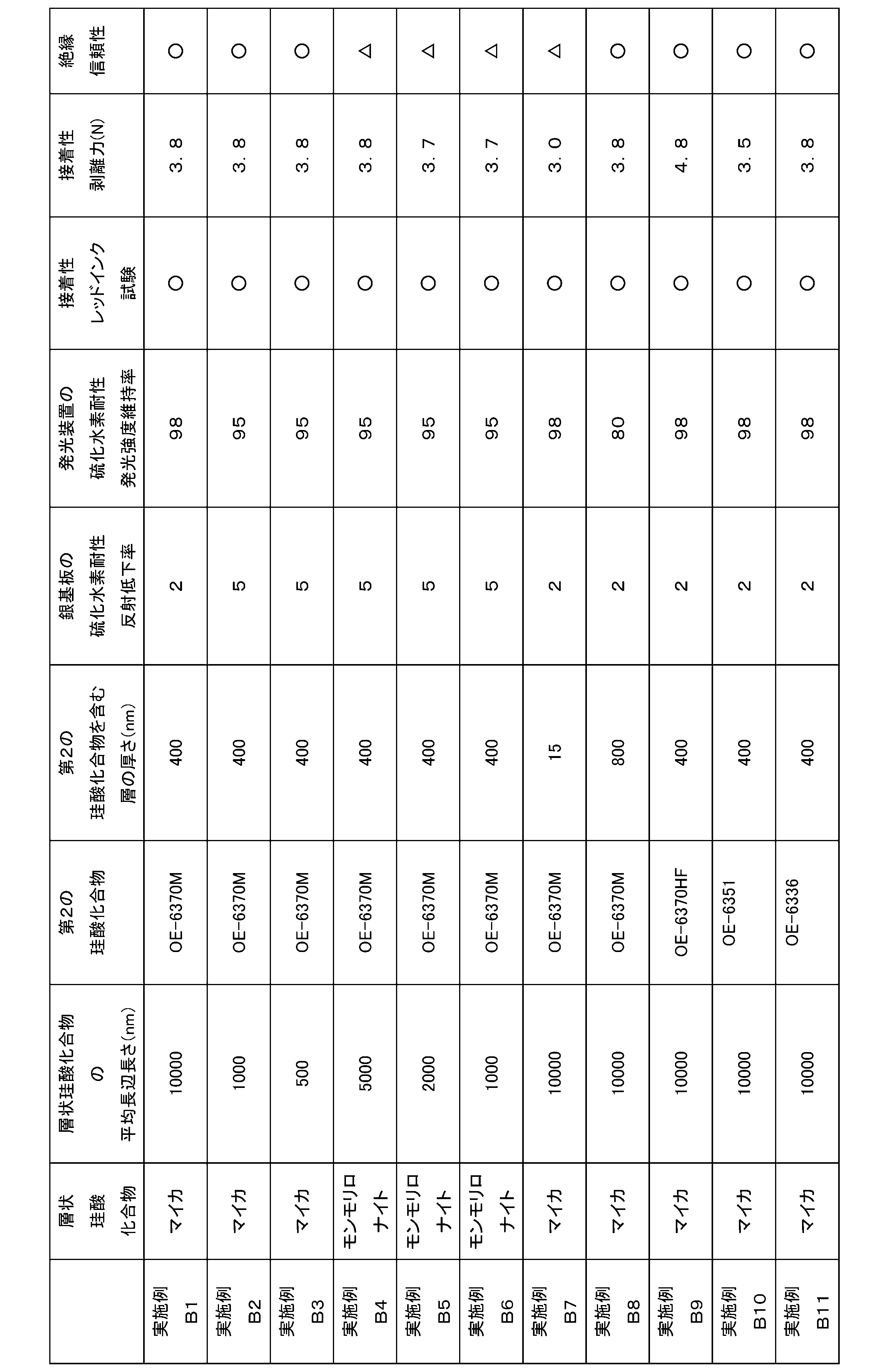
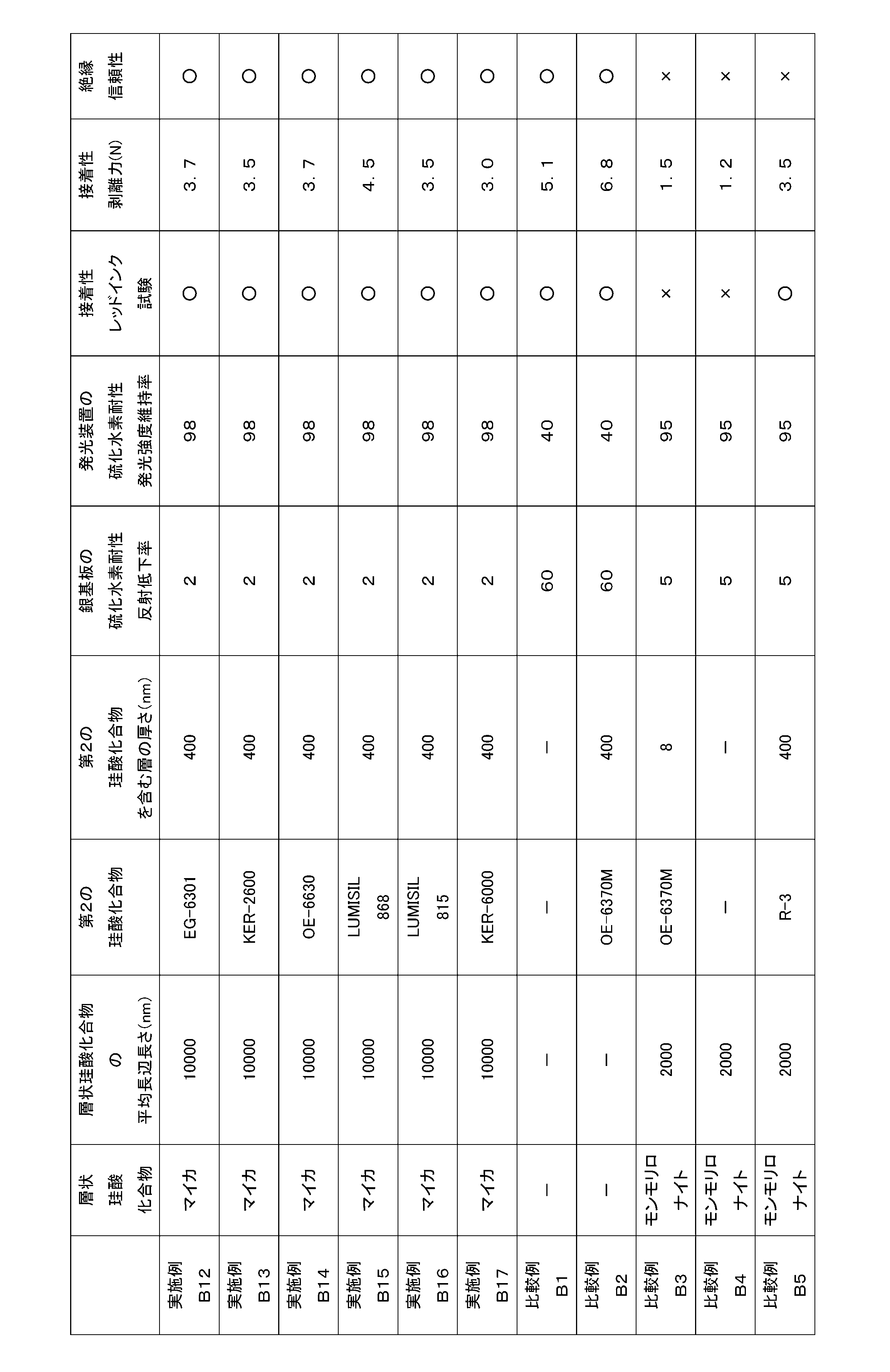
(実施例B2)
平均長辺長さ1000nmのマイカ(トピー工業株式会社製、NTS-5)を使用し、このマイカ1gに蒸留水を添加して全重量100gとした以外は実施例B1と同様にして表面処理剤を作製し、実施例B1と同様に評価を行った。結果を表2に示す。
平均長辺長さ1000nmのマイカ(トピー工業株式会社製、NTS-5)を使用し、このマイカ1gに蒸留水を添加して全重量100gとした以外は実施例B1と同様にして表面処理剤を作製し、実施例B1と同様に評価を行った。結果を表2に示す。
(実施例B3)
平均長辺長さ500nmのマイカ(トピー工業株式会社製、NHT-B2)を使用し、このマイカ1gに蒸留水を添加して全重量100gとした以外は実施例B1と同様にして表面処理剤を作製し、実施例B1と同様に評価を行った。結果を表2に示す。
平均長辺長さ500nmのマイカ(トピー工業株式会社製、NHT-B2)を使用し、このマイカ1gに蒸留水を添加して全重量100gとした以外は実施例B1と同様にして表面処理剤を作製し、実施例B1と同様に評価を行った。結果を表2に示す。
(実施例B4)
平均長辺長さ5000nmのモンモリロナイト(クニミネ工業株式会社製、クニピアFを使用し、このモンモリロナイト1gに蒸留水を添加して全重量100gとした以外は実施例B1と同様にして表面処理剤を作製し、実施例B1と同様に評価を行った。結果を表2に示す。
平均長辺長さ5000nmのモンモリロナイト(クニミネ工業株式会社製、クニピアFを使用し、このモンモリロナイト1gに蒸留水を添加して全重量100gとした以外は実施例B1と同様にして表面処理剤を作製し、実施例B1と同様に評価を行った。結果を表2に示す。
(実施例B5)
平均長辺長さ2000nmのモンモリロナイト(クニミネ工業株式会社製、クニピアF)を使用し、このモンモリロナイト1gに蒸留水を添加して全重量100gとした以外は実施例B1と同様にして表面処理剤を作製し、実施例B1と同様に評価を行った。結果を表2に示す。
平均長辺長さ2000nmのモンモリロナイト(クニミネ工業株式会社製、クニピアF)を使用し、このモンモリロナイト1gに蒸留水を添加して全重量100gとした以外は実施例B1と同様にして表面処理剤を作製し、実施例B1と同様に評価を行った。結果を表2に示す。
(実施例B6)
平均長辺長さ1000nmのモンモリロナイト(クニミネ工業株式会社製、クニピアF)を使用し、このモンモリロナイト1gに蒸留水を添加して全重量100gとした以外は実施例B1と同様にして表面処理剤を作製し、実施例B1と同様に評価を行った。結果を表2に示す。
平均長辺長さ1000nmのモンモリロナイト(クニミネ工業株式会社製、クニピアF)を使用し、このモンモリロナイト1gに蒸留水を添加して全重量100gとした以外は実施例B1と同様にして表面処理剤を作製し、実施例B1と同様に評価を行った。結果を表2に示す。
(実施例B7)
第2の珪酸化合物として、ダウコーニング製シリコーン樹脂(OE-6370M)0.05gにノルマルヘプタン99.5gを添加し、全重量を100gとして調製した以外は、実施例B1と同様にして表面処理剤を作製し、実施例B1と同様に評価を行った。結果を表2に示す。
第2の珪酸化合物として、ダウコーニング製シリコーン樹脂(OE-6370M)0.05gにノルマルヘプタン99.5gを添加し、全重量を100gとして調製した以外は、実施例B1と同様にして表面処理剤を作製し、実施例B1と同様に評価を行った。結果を表2に示す。
(実施例B8)
第2の珪酸化合物として、ダウコーニング製シリコーン樹脂(OE-6370M)6gにノルマルヘプタン94gを添加し、全重量を100gとして調製した以外は、実施例B1と同様にして表面処理剤を作製し、実施例B1と同様に評価を行った。結果を表2に示す。
第2の珪酸化合物として、ダウコーニング製シリコーン樹脂(OE-6370M)6gにノルマルヘプタン94gを添加し、全重量を100gとして調製した以外は、実施例B1と同様にして表面処理剤を作製し、実施例B1と同様に評価を行った。結果を表2に示す。
(実施例B9)
第2の珪酸化合物として、ダウコーニング製シリコーン樹脂(OE-6370HF)3gにノルマルヘプタン97gを添加し、全重量を100gとして調製した以外は、実施例B1と同様にして表面処理剤を作製し、実施例B1と同様に評価を行った。結果を表2に示す。
第2の珪酸化合物として、ダウコーニング製シリコーン樹脂(OE-6370HF)3gにノルマルヘプタン97gを添加し、全重量を100gとして調製した以外は、実施例B1と同様にして表面処理剤を作製し、実施例B1と同様に評価を行った。結果を表2に示す。
(実施例B10)
第2の珪酸化合物として、ダウコーニング製シリコーン樹脂(OE-6351)3gにノルマルヘプタン97gを添加し、全重量を100gとして調製した以外は、実施例B1と同様にして表面処理剤を作製し、実施例B1と同様に評価を行った。結果を表2に示す。
第2の珪酸化合物として、ダウコーニング製シリコーン樹脂(OE-6351)3gにノルマルヘプタン97gを添加し、全重量を100gとして調製した以外は、実施例B1と同様にして表面処理剤を作製し、実施例B1と同様に評価を行った。結果を表2に示す。
(実施例B11)
第2の珪酸化合物として、ダウコーニング製シリコーン樹脂(OE-6336)3gにノルマルヘプタン97gを添加し、全重量を100gとして調製した以外は、実施例B1と同様にして表面処理剤を作製し、実施例B1と同様に評価を行った。結果を表2に示す。
第2の珪酸化合物として、ダウコーニング製シリコーン樹脂(OE-6336)3gにノルマルヘプタン97gを添加し、全重量を100gとして調製した以外は、実施例B1と同様にして表面処理剤を作製し、実施例B1と同様に評価を行った。結果を表2に示す。
(実施例B12)
第2の珪酸化合物として、ダウコーニング製シリコーン樹脂(EG-6301)3gにノルマルヘプタン97gを添加し、全重量を100gとして調製した以外は、実施例B1と同様にして表面処理剤を作製し、実施例B1と同様に評価を行った。結果を表3に示す。
第2の珪酸化合物として、ダウコーニング製シリコーン樹脂(EG-6301)3gにノルマルヘプタン97gを添加し、全重量を100gとして調製した以外は、実施例B1と同様にして表面処理剤を作製し、実施例B1と同様に評価を行った。結果を表3に示す。
(実施例B13)
第2の珪酸化合物として、信越化学製シリコーン樹脂(KER-2600)3gにノルマルヘプタン97gを添加し、全重量を100gとして調製した以外は、実施例B1と同様にして表面処理剤を作製し、実施例B1と同様に評価を行った。結果を表3に示す。
第2の珪酸化合物として、信越化学製シリコーン樹脂(KER-2600)3gにノルマルヘプタン97gを添加し、全重量を100gとして調製した以外は、実施例B1と同様にして表面処理剤を作製し、実施例B1と同様に評価を行った。結果を表3に示す。
(実施例B14)
第2の珪酸化合物として、ダウコーニング製シリコーン樹脂(OE-6630)3gにノルマルヘプタン97gを添加し、全重量を100gとして調製した以外は、実施例B1と同様にして表面処理剤を作製し、実施例B1と同様に評価を行った。結果を表3に示す。
第2の珪酸化合物として、ダウコーニング製シリコーン樹脂(OE-6630)3gにノルマルヘプタン97gを添加し、全重量を100gとして調製した以外は、実施例B1と同様にして表面処理剤を作製し、実施例B1と同様に評価を行った。結果を表3に示す。
(実施例B15)
第2の珪酸化合物として、WACKER製シリコーン樹脂(LUMISIL868)3gにノルマルヘプタン97gを添加し、全重量を100gとして調製した以外は、実施例B1と同様にして表面処理剤を作製し、実施例B1と同様に評価を行った。結果を表3に示す。
第2の珪酸化合物として、WACKER製シリコーン樹脂(LUMISIL868)3gにノルマルヘプタン97gを添加し、全重量を100gとして調製した以外は、実施例B1と同様にして表面処理剤を作製し、実施例B1と同様に評価を行った。結果を表3に示す。
(実施例B16)
第2の珪酸化合物として、WACKER製シリコーン樹脂(LUMISIL815)3gにノルマルヘプタン97gを添加し、全重量を100gとして調製した以外は、実施例B1と同様にして表面処理剤を作製し、実施例B1と同様に評価を行った。結果を表3に示す。
第2の珪酸化合物として、WACKER製シリコーン樹脂(LUMISIL815)3gにノルマルヘプタン97gを添加し、全重量を100gとして調製した以外は、実施例B1と同様にして表面処理剤を作製し、実施例B1と同様に評価を行った。結果を表3に示す。
(実施例B17)
第2の珪酸化合物として、信越化学製シリコーン樹脂(KER-6000)3gにノルマルヘプタン97gを添加し、全重量を100gとして調製した以外は、実施例B1と同様にして表面処理剤を作製し、実施例B1と同様に評価を行った。結果を表3に示す。
第2の珪酸化合物として、信越化学製シリコーン樹脂(KER-6000)3gにノルマルヘプタン97gを添加し、全重量を100gとして調製した以外は、実施例B1と同様にして表面処理剤を作製し、実施例B1と同様に評価を行った。結果を表3に示す。
(比較例B1)
表面処理剤を用いずに銀基板及び発光装置を作製し、実施例B1と同様に評価を行った。結果を表3に示す。
表面処理剤を用いずに銀基板及び発光装置を作製し、実施例B1と同様に評価を行った。結果を表3に示す。
(比較例B2)
層状珪酸化合物を含む表面処理剤Aを用いずに銀基板及び発光装置を作製し、実施例B1と同様に評価を行った。結果を表3に示す。
層状珪酸化合物を含む表面処理剤Aを用いずに銀基板及び発光装置を作製し、実施例B1と同様に評価を行った。結果を表3に示す。
(比較例B3)
第2の珪酸化合物の膜厚を8nmとした以外は、実施例B5と同様にして表面処理剤を作製し、実施例B1と同様に評価を行った。結果を表3に示す。
第2の珪酸化合物の膜厚を8nmとした以外は、実施例B5と同様にして表面処理剤を作製し、実施例B1と同様に評価を行った。結果を表3に示す。
(比較例B4)
第2の珪酸化合物を含む表面処理剤Bを用いずに銀基板及び発光装置を作製し、平均長辺長さ1000nmのモンモリロナイト(クニミネ工業株式会社製、クニピアF)を使用し、このモンモリロナイト1gに蒸留水を添加して全重量100gとした以外は実施例B1と同様に評価を行った。結果を表3に示す。
第2の珪酸化合物を含む表面処理剤Bを用いずに銀基板及び発光装置を作製し、平均長辺長さ1000nmのモンモリロナイト(クニミネ工業株式会社製、クニピアF)を使用し、このモンモリロナイト1gに蒸留水を添加して全重量100gとした以外は実施例B1と同様に評価を行った。結果を表3に示す。
(比較例B5)
第2の珪酸化合物として、信越化学製プライマ(R-3)3gに酢酸エチル97gを添加し、全重量を100gとして調製した以外は、実施例B1と同様にして表面処理剤を作製し、実施例B1と同様に評価を行った。結果を表3に示す。
第2の珪酸化合物として、信越化学製プライマ(R-3)3gに酢酸エチル97gを添加し、全重量を100gとして調製した以外は、実施例B1と同様にして表面処理剤を作製し、実施例B1と同様に評価を行った。結果を表3に示す。
層状珪酸化合物は、超音波分散機で破砕し、平均長辺長さを所定の大きさに調整して用いた。
<酸素透過率の測定>
表4に記載の層状珪酸化合物を5質量%、水を95質量%になるよう秤量・混合し、自転・公転ミキサー(株式会社シンキー製、ARE-310)を用いて2000rpmで10分混合、2200rpmで10分脱泡を行った。
表4に記載の層状珪酸化合物を5質量%、水を95質量%になるよう秤量・混合し、自転・公転ミキサー(株式会社シンキー製、ARE-310)を用いて2000rpmで10分混合、2200rpmで10分脱泡を行った。
易接着層付きPETフィルム(東洋紡製、A4300-125)上に、wet厚100μmのバーコーターを用いて、上記で得られた層状珪酸化合物5質量%の表面処理剤を塗布後、22℃で12時間静置して溶媒を除去し、層状珪酸化合物膜を表面に具備するPETフィルムを得た。JIS K7126-1(GC法)に則って層状珪酸化合物膜を表面に具備するPETフィルムの酸素透過率を測定した。結果を表4に示す。
<体積抵抗率の測定>
表5に記載の第2の珪酸化合物3gを銅電極付き基板に塗布し、150℃で3時間乾燥させ、体積抵抗率測定試験片とした。JIS C2139に則って体積抵抗率を測定した。結果を表5に示す。
表5に記載の第2の珪酸化合物3gを銅電極付き基板に塗布し、150℃で3時間乾燥させ、体積抵抗率測定試験片とした。JIS C2139に則って体積抵抗率を測定した。結果を表5に示す。

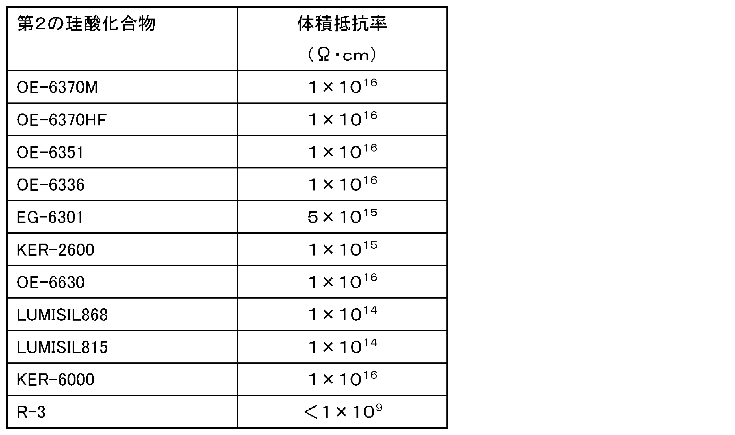
表2及び表3に示されるように、実施例B1~B17では、銀基板の硫化水素ガス耐性、発光ダイオードの硫化水素ガス耐性が得られることがわかる。また、発光ダイオードを用いた発光装置に好適な接着性が得られることがわかる。さらに、良好な絶縁信頼性を得られることがわかる。
1~4…光半導体装置、10…基板、10a…表面、12…基体、14…銅めっき板、16…銀めっき層、20…リフレクタ(光反射部)、20a…光反射面、20b…頂面、20c…外周面、20d…上端部、22…内側空間、30…青色発光ダイオード、32…ダイボンド材、34…ボンディングワイヤ、40…透明封止部、42…蛍光体、44…透明封止樹脂、50…ガスバリア層、60…プライマ層、60a…プライマ層反射面部、63…プライマ層、63a…プライマ層反射面部、63b…先端面、64…プライマ層、64a…プライマ層反射面部、64b…プライマ層頂面部、L…粘土希釈液、M…プライマ希釈液、U…露出部。
101~106…光半導体装置、108…中間部品、110…基板、110a…表面、112…基体、114…銅めっき板、116…銀めっき層、120…リフレクタ(光反射部)、120a…光反射面、120b…頂面、120c…外周面、122…内側空間、124…開口、130…青色発光ダイオード(発光ダイオード)、132…ダイボンド材、134…ボンディングワイヤ、140…透明封止部、142…蛍光体、150…ガスバリア層、151…ガスバリア層、152…第二ガスバリア層、153…第二ガスバリア層、153a…光反射面覆部、153b…ボンディングワイヤ覆部、154…第二ガスバリア層、154a…光反射面覆部、154b…ボンディングワイヤ覆部、155…ガスバリア層、160…プライマ層、L…粘土希釈液。
201…発光装置、210…基板、210a…基板の表面、212…基体、214…銅めっき板、216…銀めっき層、220…リフレクタ(光反射部)、220a…内周面(光反射面)、220b…頂面、220c…外周面、222…内側空間、230…青色LED(青色発光ダイオード)、232…ダイボンド材、234…ボンディングワイヤ、240…透明封止樹脂(透明封止部)、242…蛍光体、250…第2層(プライマ層)、252…第1層(ガスバリア層)、260…複層膜(変色防止膜)、M…B液。
Claims (12)
- 表面に銀めっき層が形成された基板と、
前記銀めっき層にボンディングされた発光ダイオードと、
前記発光ダイオードを取り囲む光反射面により前記発光ダイオードを収容する内側空間を形成する光反射部と、
前記銀めっき層を被覆する銀硫化防止膜と、
前記内側空間に充填されて前記発光ダイオードを封止する透明封止部と、
を備え、
前記銀硫化防止膜は、
粘土によるガスバリア性を有するガスバリア層と、
前記ガスバリア層の下層に配置されて接着性を有するプライマ層と、
を有し、
前記透明封止部と前記プライマ層とが接触している、
光半導体装置。 - 前記プライマ層は、前記光反射面上に形成されており、
前記ガスバリア層は、前記光反射面上において前記プライマ層の一部に積層されており、
前記透明封止部は、前記光反射面上の、前記ガスバリア層が前記プライマ層に積層されていない位置において、前記ガスバリア層と接触している、
請求項1に記載の光半導体装置。 - 前記発光ダイオードは、青色光を発生する青色発光ダイオードである、
請求項2に記載の光半導体装置。 - 表面に銀めっき層が形成された基板と、
前記銀めっき層にボンディングされた発光ダイオードと、
前記発光ダイオードを取り囲む光反射面により前記発光ダイオードを収容する内側空間を形成する光反射部と、
前記内側空間に充填されて前記発光ダイオードを封止する透明封止部と、
前記基板から離れた位置に形成されて、粘土によるガスバリア性を有するガスバリア層と、
を備える、
光半導体装置。 - 前記ガスバリア層と前記基板との間に、前記透明封止部が配置されている、
請求項4に記載の光半導体装置。 - 前記ガスバリア層は、前記透明封止部に埋設されている、
請求項4又は5に記載の光半導体装置。 - 銀めっき層を有する基板と、前記基板上に搭載された発光ダイオードと、少なくとも前記銀めっき層の表面を被覆する複層膜と、を備え、
前記複層膜が、層状珪酸化合物を含有する第1層と、前記層状珪酸化合物以外の第2の珪酸化合物を含有する第2層と、を有する、発光装置。 - 前記銀めっき層の表面に、前記第2層と、前記第1層とがこの順に設けられている、請求項7に記載の発光装置。
- 透明封止樹脂によって被覆又は封止された、請求項7又は8に記載の発光装置。
- 銀めっき層を有する基板と、前記基板上に搭載された発光ダイオードと、少なくとも前記銀めっき層の表面を被覆する複層膜と、を備え、
前記複層膜が、酸素透過率0.0001~10cc/m2・24h・atmである化合物を含有する第1層と、体積抵抗率1010~1016Ω・cmである化合物を含有する第2層と、を有する、発光装置。 - 前記銀めっき層の表面に、前記第2層と、前記第1層とがこの順に設けられている、請求項10に記載の発光装置。
- 透明封止樹脂によって被覆又は封止された、請求項10又は11に記載の発光装置。
Priority Applications (2)
| Application Number | Priority Date | Filing Date | Title |
|---|---|---|---|
| KR1020167018624A KR20160097332A (ko) | 2013-12-11 | 2014-12-11 | 광 반도체 장치 및 그 제조 방법, 및 은용 표면 처리제 및 발광 장치 |
| CN201480066824.7A CN105814701B (zh) | 2013-12-11 | 2014-12-11 | 光半导体装置及其制造方法以及银用表面处理剂及发光装置 |
Applications Claiming Priority (8)
| Application Number | Priority Date | Filing Date | Title |
|---|---|---|---|
| JP2013-256503 | 2013-12-11 | ||
| JP2013256503A JP6269007B2 (ja) | 2013-12-11 | 2013-12-11 | 光半導体装置 |
| JP2014086616A JP6269284B2 (ja) | 2014-04-18 | 2014-04-18 | 銀用表面処理剤及び発光装置 |
| JP2014-086616 | 2014-04-18 | ||
| JP2014-086618 | 2014-04-18 | ||
| JP2014086618A JP2015207634A (ja) | 2014-04-18 | 2014-04-18 | 発光装置 |
| JP2014106329A JP6308020B2 (ja) | 2014-05-22 | 2014-05-22 | 光半導体装置及びその製造方法 |
| JP2014-106329 | 2014-05-22 |
Publications (1)
| Publication Number | Publication Date |
|---|---|
| WO2015087970A1 true WO2015087970A1 (ja) | 2015-06-18 |
Family
ID=53371269
Family Applications (1)
| Application Number | Title | Priority Date | Filing Date |
|---|---|---|---|
| PCT/JP2014/082838 Ceased WO2015087970A1 (ja) | 2013-12-11 | 2014-12-11 | 光半導体装置及びその製造方法、並びに銀用表面処理剤及び発光装置 |
Country Status (4)
| Country | Link |
|---|---|
| KR (1) | KR20160097332A (ja) |
| CN (1) | CN105814701B (ja) |
| TW (1) | TWI552375B (ja) |
| WO (1) | WO2015087970A1 (ja) |
Cited By (1)
| Publication number | Priority date | Publication date | Assignee | Title |
|---|---|---|---|---|
| CN114121694A (zh) * | 2021-11-19 | 2022-03-01 | 深圳市鼎华芯泰科技有限公司 | 一种改善ic封装密封性的封装方法 |
Families Citing this family (4)
| Publication number | Priority date | Publication date | Assignee | Title |
|---|---|---|---|---|
| CN107180903A (zh) * | 2017-04-21 | 2017-09-19 | 深圳市洲明科技股份有限公司 | 一种chip‑led产品及制作方法 |
| CN110190157A (zh) * | 2018-12-11 | 2019-08-30 | 深圳市长方集团股份有限公司 | 一种具有抗硫化液的led防硫化封装工艺 |
| CN110190166A (zh) * | 2018-12-11 | 2019-08-30 | 深圳市长方集团股份有限公司 | 一种具有脱模剂的led防硫化封装工艺 |
| CN110190165A (zh) * | 2018-12-11 | 2019-08-30 | 深圳市长方集团股份有限公司 | 一种具有抗硫化液和脱模剂的led防硫化封装工艺 |
Citations (8)
| Publication number | Priority date | Publication date | Assignee | Title |
|---|---|---|---|---|
| JP2004339450A (ja) * | 2003-05-19 | 2004-12-02 | Kanegafuchi Chem Ind Co Ltd | プライマー組成物、及び該プライマーを用いた発光ダイオード |
| JP2006077237A (ja) * | 2004-08-10 | 2006-03-23 | National Institute Of Advanced Industrial & Technology | 粘土配向膜からなる保護膜 |
| JP2010004035A (ja) * | 2008-05-22 | 2010-01-07 | Mitsubishi Chemicals Corp | 半導体発光装置、照明装置、および画像表示装置 |
| JP2010007013A (ja) * | 2008-06-30 | 2010-01-14 | Jsr Corp | 金属表面用コート材および発光装置、並びに金属表面保護方法 |
| JP2012046553A (ja) * | 2010-08-24 | 2012-03-08 | Aica Kogyo Co Ltd | プライマー組成物および封止構造体 |
| JP2012251204A (ja) * | 2011-06-02 | 2012-12-20 | Hitachi Chemical Co Ltd | 銀及び銀合金の表面処理剤、光反射膜付き基板並びに発光装置 |
| WO2013108773A1 (ja) * | 2012-01-16 | 2013-07-25 | 日立化成株式会社 | 銀の表面処理剤及び発光装置 |
| JP2013214760A (ja) * | 2013-06-05 | 2013-10-17 | Sharp Corp | 発光装置およびその製造方法 |
Family Cites Families (5)
| Publication number | Priority date | Publication date | Assignee | Title |
|---|---|---|---|---|
| JPH10158572A (ja) | 1996-11-28 | 1998-06-16 | Dainippon Ink & Chem Inc | 銀被覆塗料用組成物 |
| JP4181888B2 (ja) | 2003-02-04 | 2008-11-19 | 四国化成工業株式会社 | 銀及び銀合金の防食処理剤 |
| EP2768031B1 (en) | 2005-08-04 | 2021-02-17 | Nichia Corporation | Light-emitting device |
| EP2085411A3 (en) * | 2008-01-22 | 2009-08-26 | JSR Corporation | Metal-coating material, method for protecting metal, and light emitting device |
| JP5289835B2 (ja) * | 2008-06-25 | 2013-09-11 | シャープ株式会社 | 発光装置およびその製造方法 |
-
2014
- 2014-12-11 TW TW103143340A patent/TWI552375B/zh not_active IP Right Cessation
- 2014-12-11 CN CN201480066824.7A patent/CN105814701B/zh not_active Expired - Fee Related
- 2014-12-11 WO PCT/JP2014/082838 patent/WO2015087970A1/ja not_active Ceased
- 2014-12-11 KR KR1020167018624A patent/KR20160097332A/ko not_active Ceased
Patent Citations (9)
| Publication number | Priority date | Publication date | Assignee | Title |
|---|---|---|---|---|
| JP2004339450A (ja) * | 2003-05-19 | 2004-12-02 | Kanegafuchi Chem Ind Co Ltd | プライマー組成物、及び該プライマーを用いた発光ダイオード |
| JP2006077237A (ja) * | 2004-08-10 | 2006-03-23 | National Institute Of Advanced Industrial & Technology | 粘土配向膜からなる保護膜 |
| JP2010004035A (ja) * | 2008-05-22 | 2010-01-07 | Mitsubishi Chemicals Corp | 半導体発光装置、照明装置、および画像表示装置 |
| JP2010007013A (ja) * | 2008-06-30 | 2010-01-14 | Jsr Corp | 金属表面用コート材および発光装置、並びに金属表面保護方法 |
| JP2012046553A (ja) * | 2010-08-24 | 2012-03-08 | Aica Kogyo Co Ltd | プライマー組成物および封止構造体 |
| JP2012251204A (ja) * | 2011-06-02 | 2012-12-20 | Hitachi Chemical Co Ltd | 銀及び銀合金の表面処理剤、光反射膜付き基板並びに発光装置 |
| WO2013108773A1 (ja) * | 2012-01-16 | 2013-07-25 | 日立化成株式会社 | 銀の表面処理剤及び発光装置 |
| JP5637322B2 (ja) * | 2012-01-16 | 2014-12-10 | 日立化成株式会社 | 銀の表面処理剤及び発光装置 |
| JP2013214760A (ja) * | 2013-06-05 | 2013-10-17 | Sharp Corp | 発光装置およびその製造方法 |
Cited By (1)
| Publication number | Priority date | Publication date | Assignee | Title |
|---|---|---|---|---|
| CN114121694A (zh) * | 2021-11-19 | 2022-03-01 | 深圳市鼎华芯泰科技有限公司 | 一种改善ic封装密封性的封装方法 |
Also Published As
| Publication number | Publication date |
|---|---|
| TWI552375B (zh) | 2016-10-01 |
| CN105814701B (zh) | 2019-03-12 |
| CN105814701A (zh) | 2016-07-27 |
| KR20160097332A (ko) | 2016-08-17 |
| TW201535773A (zh) | 2015-09-16 |
Similar Documents
| Publication | Publication Date | Title |
|---|---|---|
| JP5637322B2 (ja) | 銀の表面処理剤及び発光装置 | |
| JP6107510B2 (ja) | 発光装置及びその製造方法 | |
| WO2015087970A1 (ja) | 光半導体装置及びその製造方法、並びに銀用表面処理剤及び発光装置 | |
| KR101690627B1 (ko) | 은 황화 방지재, 은 황화 방지막의 형성 방법, 발광 장치의 제조 방법 및 발광 장치 | |
| JP6269284B2 (ja) | 銀用表面処理剤及び発光装置 | |
| WO2013183706A1 (ja) | 光半導体装置 | |
| JP2012153827A (ja) | 電極腐食防止剤、電極腐食防止剤を用いた発光デバイス | |
| JP2015207634A (ja) | 発光装置 | |
| JP6203479B2 (ja) | 光半導体装置、その製造方法、その製造に用いる基体およびリフレクタ成型体 | |
| JP5949184B2 (ja) | 光半導体装置の製造方法 | |
| JP6308020B2 (ja) | 光半導体装置及びその製造方法 | |
| JP6269007B2 (ja) | 光半導体装置 | |
| JP6203478B2 (ja) | 光半導体装置、その製造方法、その製造に用いる基体およびリフレクタ成型体 | |
| JP5939045B2 (ja) | 銀硫化防止材、銀硫化防止膜の形成方法及び発光装置の製造方法 | |
| JP2015233081A (ja) | 光半導体装置の製造方法及び光半導体装置 | |
| JP6007637B2 (ja) | 光半導体装置、その製造方法、その製造に用いる基体およびリフレクタ成型体 | |
| JP6051820B2 (ja) | 銀硫化防止材、銀硫化防止膜の形成方法及び発光装置の製造方法 | |
| JP6011037B2 (ja) | 光半導体装置、その製造方法、その製造に用いる基体およびリフレクタ成型体 | |
| JP5939044B2 (ja) | 銀硫化防止材、銀硫化防止膜の形成方法、発光装置の製造方法及び発光装置 |
Legal Events
| Date | Code | Title | Description |
|---|---|---|---|
| 121 | Ep: the epo has been informed by wipo that ep was designated in this application |
Ref document number: 14870347 Country of ref document: EP Kind code of ref document: A1 |
|
| NENP | Non-entry into the national phase |
Ref country code: DE |
|
| ENP | Entry into the national phase |
Ref document number: 20167018624 Country of ref document: KR Kind code of ref document: A |
|
| 122 | Ep: pct application non-entry in european phase |
Ref document number: 14870347 Country of ref document: EP Kind code of ref document: A1 |