WO2015087861A1 - 蛍光体、およびその製造方法、ならびにその蛍光体を用いた発光装置 - Google Patents
蛍光体、およびその製造方法、ならびにその蛍光体を用いた発光装置 Download PDFInfo
- Publication number
- WO2015087861A1 WO2015087861A1 PCT/JP2014/082516 JP2014082516W WO2015087861A1 WO 2015087861 A1 WO2015087861 A1 WO 2015087861A1 JP 2014082516 W JP2014082516 W JP 2014082516W WO 2015087861 A1 WO2015087861 A1 WO 2015087861A1
- Authority
- WO
- WIPO (PCT)
- Prior art keywords
- phosphor
- light emitting
- light
- emitting device
- fluorescent substance
- Prior art date
- Legal status (The legal status is an assumption and is not a legal conclusion. Google has not performed a legal analysis and makes no representation as to the accuracy of the status listed.)
- Ceased
Links
Images


Classifications
-
- C—CHEMISTRY; METALLURGY
- C09—DYES; PAINTS; POLISHES; NATURAL RESINS; ADHESIVES; COMPOSITIONS NOT OTHERWISE PROVIDED FOR; APPLICATIONS OF MATERIALS NOT OTHERWISE PROVIDED FOR
- C09K—MATERIALS FOR MISCELLANEOUS APPLICATIONS, NOT PROVIDED FOR ELSEWHERE
- C09K11/00—Luminescent materials, e.g. electroluminescent or chemiluminescent
- C09K11/08—Luminescent materials, e.g. electroluminescent or chemiluminescent containing inorganic luminescent materials
- C09K11/61—Luminescent materials, e.g. electroluminescent or chemiluminescent containing inorganic luminescent materials containing fluorine, chlorine, bromine, iodine or unspecified halogen elements
- C09K11/615—Halogenides
- C09K11/616—Halogenides with alkali or alkaline earth metals
-
- C—CHEMISTRY; METALLURGY
- C09—DYES; PAINTS; POLISHES; NATURAL RESINS; ADHESIVES; COMPOSITIONS NOT OTHERWISE PROVIDED FOR; APPLICATIONS OF MATERIALS NOT OTHERWISE PROVIDED FOR
- C09K—MATERIALS FOR MISCELLANEOUS APPLICATIONS, NOT PROVIDED FOR ELSEWHERE
- C09K11/00—Luminescent materials, e.g. electroluminescent or chemiluminescent
- C09K11/08—Luminescent materials, e.g. electroluminescent or chemiluminescent containing inorganic luminescent materials
- C09K11/57—Luminescent materials, e.g. electroluminescent or chemiluminescent containing inorganic luminescent materials containing manganese or rhenium
-
- C—CHEMISTRY; METALLURGY
- C09—DYES; PAINTS; POLISHES; NATURAL RESINS; ADHESIVES; COMPOSITIONS NOT OTHERWISE PROVIDED FOR; APPLICATIONS OF MATERIALS NOT OTHERWISE PROVIDED FOR
- C09K—MATERIALS FOR MISCELLANEOUS APPLICATIONS, NOT PROVIDED FOR ELSEWHERE
- C09K11/00—Luminescent materials, e.g. electroluminescent or chemiluminescent
- C09K11/08—Luminescent materials, e.g. electroluminescent or chemiluminescent containing inorganic luminescent materials
- C09K11/59—Luminescent materials, e.g. electroluminescent or chemiluminescent containing inorganic luminescent materials containing silicon
-
- C—CHEMISTRY; METALLURGY
- C09—DYES; PAINTS; POLISHES; NATURAL RESINS; ADHESIVES; COMPOSITIONS NOT OTHERWISE PROVIDED FOR; APPLICATIONS OF MATERIALS NOT OTHERWISE PROVIDED FOR
- C09K—MATERIALS FOR MISCELLANEOUS APPLICATIONS, NOT PROVIDED FOR ELSEWHERE
- C09K11/00—Luminescent materials, e.g. electroluminescent or chemiluminescent
- C09K11/08—Luminescent materials, e.g. electroluminescent or chemiluminescent containing inorganic luminescent materials
- C09K11/61—Luminescent materials, e.g. electroluminescent or chemiluminescent containing inorganic luminescent materials containing fluorine, chlorine, bromine, iodine or unspecified halogen elements
- C09K11/617—Silicates
-
- H—ELECTRICITY
- H10—SEMICONDUCTOR DEVICES; ELECTRIC SOLID-STATE DEVICES NOT OTHERWISE PROVIDED FOR
- H10H—INORGANIC LIGHT-EMITTING SEMICONDUCTOR DEVICES HAVING POTENTIAL BARRIERS
- H10H20/00—Individual inorganic light-emitting semiconductor devices having potential barriers, e.g. light-emitting diodes [LED]
- H10H20/80—Constructional details
- H10H20/85—Packages
- H10H20/851—Wavelength conversion means
- H10H20/8511—Wavelength conversion means characterised by their material, e.g. binder
- H10H20/8512—Wavelength conversion materials
-
- H—ELECTRICITY
- H10—SEMICONDUCTOR DEVICES; ELECTRIC SOLID-STATE DEVICES NOT OTHERWISE PROVIDED FOR
- H10H—INORGANIC LIGHT-EMITTING SEMICONDUCTOR DEVICES HAVING POTENTIAL BARRIERS
- H10H20/00—Individual inorganic light-emitting semiconductor devices having potential barriers, e.g. light-emitting diodes [LED]
- H10H20/80—Constructional details
- H10H20/85—Packages
- H10H20/851—Wavelength conversion means
- H10H20/8511—Wavelength conversion means characterised by their material, e.g. binder
- H10H20/8512—Wavelength conversion materials
- H10H20/8513—Wavelength conversion materials having two or more wavelength conversion materials
-
- H—ELECTRICITY
- H10—SEMICONDUCTOR DEVICES; ELECTRIC SOLID-STATE DEVICES NOT OTHERWISE PROVIDED FOR
- H10H—INORGANIC LIGHT-EMITTING SEMICONDUCTOR DEVICES HAVING POTENTIAL BARRIERS
- H10H20/00—Individual inorganic light-emitting semiconductor devices having potential barriers, e.g. light-emitting diodes [LED]
- H10H20/80—Constructional details
- H10H20/85—Packages
- H10H20/857—Interconnections, e.g. lead-frames, bond wires or solder balls
-
- H—ELECTRICITY
- H10—SEMICONDUCTOR DEVICES; ELECTRIC SOLID-STATE DEVICES NOT OTHERWISE PROVIDED FOR
- H10W—GENERIC PACKAGES, INTERCONNECTIONS, CONNECTORS OR OTHER CONSTRUCTIONAL DETAILS OF DEVICES COVERED BY CLASS H10
- H10W72/00—Interconnections or connectors in packages
- H10W72/50—Bond wires
- H10W72/531—Shapes of wire connectors
- H10W72/536—Shapes of wire connectors the connected ends being ball-shaped
-
- H—ELECTRICITY
- H10—SEMICONDUCTOR DEVICES; ELECTRIC SOLID-STATE DEVICES NOT OTHERWISE PROVIDED FOR
- H10W—GENERIC PACKAGES, INTERCONNECTIONS, CONNECTORS OR OTHER CONSTRUCTIONAL DETAILS OF DEVICES COVERED BY CLASS H10
- H10W72/00—Interconnections or connectors in packages
- H10W72/50—Bond wires
- H10W72/531—Shapes of wire connectors
- H10W72/5363—Shapes of wire connectors the connected ends being wedge-shaped
-
- H—ELECTRICITY
- H10—SEMICONDUCTOR DEVICES; ELECTRIC SOLID-STATE DEVICES NOT OTHERWISE PROVIDED FOR
- H10W—GENERIC PACKAGES, INTERCONNECTIONS, CONNECTORS OR OTHER CONSTRUCTIONAL DETAILS OF DEVICES COVERED BY CLASS H10
- H10W72/00—Interconnections or connectors in packages
- H10W72/851—Dispositions of multiple connectors or interconnections
- H10W72/874—On different surfaces
- H10W72/884—Die-attach connectors and bond wires
-
- H—ELECTRICITY
- H10—SEMICONDUCTOR DEVICES; ELECTRIC SOLID-STATE DEVICES NOT OTHERWISE PROVIDED FOR
- H10W—GENERIC PACKAGES, INTERCONNECTIONS, CONNECTORS OR OTHER CONSTRUCTIONAL DETAILS OF DEVICES COVERED BY CLASS H10
- H10W74/00—Encapsulations, e.g. protective coatings
-
- H—ELECTRICITY
- H10—SEMICONDUCTOR DEVICES; ELECTRIC SOLID-STATE DEVICES NOT OTHERWISE PROVIDED FOR
- H10W—GENERIC PACKAGES, INTERCONNECTIONS, CONNECTORS OR OTHER CONSTRUCTIONAL DETAILS OF DEVICES COVERED BY CLASS H10
- H10W90/00—Package configurations
- H10W90/701—Package configurations characterised by the relative positions of pads or connectors relative to package parts
- H10W90/751—Package configurations characterised by the relative positions of pads or connectors relative to package parts of bond wires
- H10W90/756—Package configurations characterised by the relative positions of pads or connectors relative to package parts of bond wires between a chip and a stacked lead frame, conducting package substrate or heat sink
Definitions
- the present invention relates to a phosphor, a manufacturing method thereof, and a light emitting device using the phosphor.
- a light-emitting diode (LED) light-emitting device is mainly composed of a combination of an LED chip as an excitation light source and a phosphor, and various combinations of light emission colors can be realized.
- a white LED light emitting device that emits white light
- a combination of an LED chip that emits light in a blue region and a phosphor is used.
- a combination of an LED chip that emits blue light and a phosphor mixture may be mentioned.
- the phosphor a yellow light emitting phosphor which is a complementary color of blue is mainly used, and it is used as a pseudo white light LED light emitting device.
- a three-wavelength white LED using an LED chip that emits blue light, a green or yellow light emitting phosphor, and a red light emitting phosphor has been developed.
- a K 2 SiF 6 : Mn phosphor is known as one of red light emitting phosphors used in such a light emitting device.
- An object of the present invention is to provide a red light-emitting phosphor that emits light when excited by light having an emission peak in a blue region, a method for producing the phosphor, and a light-emitting device using the phosphor. is there.
- the red light emitting phosphor has a basic composition represented by the following formula (A): K a (Si 1-x , Mn x ) F b (A) (Wherein 1.5 ⁇ a ⁇ 2.5, 5.5 ⁇ b ⁇ 6.5, 0 ⁇ x ⁇ 0.06)
- the ratio of the intensity of the peak attributed to the Mn—F bond in the crystal in which the Raman shift is in the range of 600 ⁇ 10 cm ⁇ 1 is 0.09 or more and 0.22 or less.
- a method for producing a phosphor according to an embodiment of the present invention includes preparing an aqueous solution containing potassium permanganate and hydrogen fluoride as a reaction solution, and immersing a silicon source in the reaction solution for reaction.
- the method for producing a phosphor is characterized in that the molar ratio of hydrogen fluoride to potassium permanganate in the reaction solution is 87 or more and 127 or less.
- a light-emitting device includes a light-emitting element that emits light in a wavelength region of 440 nm to 470 nm and a phosphor layer containing the phosphor. It is.
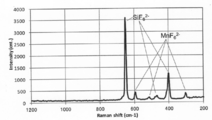
- the Raman spectrum of the fluorescent substance by embodiment The figure which shows the relationship of the ratio of the intensity
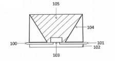
- 1 is a cross-sectional view of a light emitting device according to an embodiment of the present invention. Sectional drawing of the light-emitting device concerning other embodiment of this invention.
- the present inventors have found that the intensity of peaks attributed to each bond in the crystal is determined by the Raman spectrum of the phosphor.
- the present inventors have found that there is a correlation with the emission characteristics of the phosphor.
- the ratio of the peak intensity attributed to the Si—F bond and the peak intensity attributed to the Mn—F bond contained in the phosphor made of manganese-activated potassium silicofluoride is in a specific range.
- the present inventors have found that excellent light emission characteristics can be obtained.
- the red light-emitting phosphor according to the embodiment is a phosphor mainly made of potassium silicofluoride and activated with manganese.
- the phosphor mainly composed of potassium silicofluoride refers to a phosphor in which the basic crystal structure of the phosphor is potassium silicofluoride and a part of the elements constituting the crystal is substituted with other elements.
- the composition of the phosphor according to the embodiment is represented by the following formula (A).
- the phosphor according to the embodiment contains manganese as an activator.
- the manganese content increases, the luminous efficiency tends to be improved, and is preferably 0.01 or more.
- the valence of manganese is preferably +4.
- the manganese content (x) is generally 0.06 or less, preferably 0.05 or less.
- the synthesized phosphor is alkali-melted and analyzed by ICP emission spectroscopy using, for example, an IRIS Advantage type ICP emission spectrometer (trade name, manufactured by Thermo Fisher Scientific). can do.
- the nonmetallic element F can be separated by thermal hydrolysis of the synthesized phosphor and analyzed by, for example, a DX-120 type ion chromatograph analyzer (trade name, manufactured by Nippon Dionex Co., Ltd.). Further, F can be analyzed by ion chromatography after alkali melting as in the case of the metal element described above.
- the phosphor according to the embodiment does not contain oxygen stoichiometrically.
- oxygen may be inevitably mixed into the phosphor during the phosphor synthesis process or due to decomposition of the phosphor surface after synthesis. It is desirable that the oxygen content in the phosphor is zero, but if the value of [oxygen content] / [(fluorine content) + (oxygen content)] is less than 0.05, light emission It is preferable because the efficiency is not greatly impaired.
- the phosphor according to the embodiment may contain a small amount of alkali metal elements such as Na, Rb, and Cs, and other elements such as Ti, Ge, and Sn. Even when these elements are contained in a small amount, the phosphor exhibits a similar emission spectrum and can achieve a desired effect.
- the content of these elements is preferably small from the viewpoint of the stability of the phosphor and the reactivity during phosphor synthesis.
- a metal element other than the metal element included in the formula (A) is used. Preferably it is not.
- the phosphor composition of the formula (A) according to the embodiment can be obtained by melting and analyzing the phosphor and analyzing it.
- the phosphor according to the embodiment exists in a form in which it is present inside the phosphor, is combined with fluorine and contributes to light emission, and is combined with oxygen on the phosphor surface or the like.
- the present inventors have found that manganese that inhibits luminescence exists. That is, in ICP emission spectroscopic analysis, it is possible to measure the total amount of Mn contained in the phosphor, but there is a disadvantage that the total amount contains Mn that inhibits light emission.
- the “surface” of the phosphor includes a range from the actual surface to a depth that can be detected by XPS analysis, and “inside” refers to a portion inside it.
- Raman spectrum measurement is a method for examining the molecular structure and crystal structure unique to a sample by irradiating the sample with light and measuring the scattered light. Specifically, the phosphor is irradiated with light and the scattered light is measured. In addition to Rayleigh scattered light, the scattered light includes Raman scattered light having a wavelength different from that of the irradiated light corresponding to various atomic bonds existing in the crystal structure. Therefore, by analyzing the scattered light, it is possible to detect peaks attributed to Si—F bonds and Mn—F bonds contained in the phosphor as a sample.
- the Raman spectrum measurement can be performed with a LabRAM HR-PL apparatus (trade name, manufactured by Horiba Joban Yvon).
- the measurement conditions can vary depending on the type of phosphor to be measured, the particle shape, and the like.
- Analysis method Backscattering Raman spectrum measurement, slit width: 100 ⁇ m, Light source: semiconductor laser (785 nm), optical system: microscope (100 times body), Beam diameter: 1 ⁇ m, light source output: 15 mW Detector: CCD multi-channel integration time: 120 seconds, integration count: 3 times Sample conditions: room temperature, in air
- FIG. 1 shows the Raman spectrum of the phosphor according to the embodiment and the assignment of its peak.
- the inventors of the present invention correspond to the Si—F bond appearing in the range of 650 ⁇ 10 cm ⁇ 1 of the peak detected in the Raman spectrum among the phosphors whose composition is represented by the formula (A).
- the ratio (I 1 / I 0) of the intensity of the peak corresponding to the Mn-F bond Raman shift appears in the range of 600 ⁇ 10cm -1 (I 1) is 0.09 or more 0
- a phosphor having a particle size of .22 or less has high external quantum efficiency and internal quantum efficiency. Specifically, in the phosphor according to the embodiment, the internal quantum efficiency is 80% or more.
- Non-Patent Document 1 peaks appearing in the range of Raman shift of 650 ⁇ 10 cm ⁇ 1 and 600 ⁇ 10 cm ⁇ 1 belong to the A1g mode, which is the stretching vibration of Si—F bond and Mn—F bond, respectively.
- A1g mode is the stretching vibration of Si—F bond and Mn—F bond, respectively.
- Non-Patent Document 1 the peak attributed to the Si—F bond appearing in the range of 480 ⁇ 10 cm ⁇ 1 and the peak attributed to the Mn—F bond appearing in the range of 520 ⁇ 10 cm ⁇ 1 both belong to the Eg mode. Both the peak attributed to the Si—F bond appearing in the range of 410 ⁇ 10 cm ⁇ 1 and the peak attributed to the Mn—F bond appearing in the range of 310 ⁇ 10 cm ⁇ 1 are both attributed to the F2g (T2g) mode. Yes.
- the total amount of Mn in the phosphor whose composition is represented by the formula (A) can be quantitatively determined by ICP emission spectroscopy, but is generally used for phosphors mainly composed of potassium silicofluoride.
- Such a synthesis method often contains Mn bonded to oxygen on the phosphor surface or the like, that is, MnO x, and it is difficult to detect only Mn related to light emission by ICP emission spectroscopy.
- the amount of Mn cannot be quantitatively determined in the Raman spectrum, but the Mn—F bond directly related to light emission can be determined as the intensity ratio of the Si—F bond.
- the external quantum efficiency ⁇ is a value calculated by multiplying the absorption rate ⁇ defined below and the internal quantum efficiency ⁇ ′.
- E ( ⁇ ) the entire spectrum of the excitation light source irradiated to the phosphor (photon number conversion)
- the external quantum efficiency ( ⁇ ) can be calculated by (I) ⁇ (II).
- External quantum efficiency, internal quantum efficiency, and absorption rate can be measured by, for example, a C9920-02G type absolute PL quantum yield measuring apparatus (trade name, manufactured by Hamamatsu Photonics Co., Ltd.).
- a C9920-02G type absolute PL quantum yield measuring apparatus (trade name, manufactured by Hamamatsu Photonics Co., Ltd.).
- blue light having a peak wavelength in the vicinity of 440 to 460 nm and a half width of 5 to 15 nm can be used.
- R A1g obtained from the Raman spectrum and the internal quantum efficiency and the relationship between R A1g and the external quantum efficiency are as shown in FIGS. 2 and 3 (details will be described later). It can be seen that the internal quantum efficiency and the external quantum efficiency are good when R A1g is in the range of 0.09 to 0.22.
- the phosphor according to the embodiment can be manufactured by an arbitrary method, and specifically, can be manufactured by the following method.
- an aqueous solution containing potassium permanganate and hydrogen fluoride is prepared as a reaction solution. And by making this reaction solution contact a silicon source, reaction advances on the surface of the silicon source, and fluorescent substance is formed.
- this reaction solution has a molar ratio of hydrogen fluoride to potassium permanganate (hereinafter referred to as “r H / K ”) of 87 or more (since there was a calculation error, the numerical value was corrected. ) Is 127 or less, preferably 90 or more and / or 120 or less.
- the concentration [HF] of hydrogen fluoride in the reaction solution is preferably 27% by mass or more and 40% by mass or less, and more preferably 28% by mass or more and 35% by mass or less.
- the phosphor according to an embodiment of the present invention has a crystal structure in which Mn is substituted for a part of the Si position in the K a SiF b matrix.
- the silicon source is oxidized by potassium permanganate and converted to silica, and the silica is fluorinated by HF.
- a K a SiF b matrix is produced by an ion exchange reaction.
- potassium permanganate becomes tetravalent Mn after oxidizing the silicon source, and is taken into the K a SiF b matrix.
- the reaction in which K a SiF b is produced from silica during this reaction process is very fast.
- the production reaction of tetravalent Mn is slower than the production rate of K a SiF b .
- the production rate of K a SiF b depends on the ratio of the proton [H + ] concentration to the [K + ] concentration in the reaction solution. That is, when the HF concentration increases, the dissolution rate of silica is accelerated, and the production reaction of K a SiF b is accelerated. On the other hand, since the valence change rate of Mn does not change, if the concentration of HF is too high, the amount of Mn taken into the K a SiF b matrix decreases. As a result, it is considered that the ratio of Mn—F bonds to Si—F bonds in the phosphor decreases.
- the concentration of HF contained in the reaction solution is high because the production of K a SiF b is promoted, an excessively high concentration reduces the [K +] concentration ratio in the reaction solution, so that the ion exchange reaction. It is considered that the yield of the phosphor is significantly reduced.
- a surface layer can also be formed on the surface of the phosphor particles thus produced by a coating process, for example, in order to improve moisture resistance and applicability during device fabrication.
- the material constituting the surface layer is selected from silicone resin, epoxy resin, fluororesin, tetraethoxysilane (TEOS), silica, zinc silicate, aluminum silicate, calcium polyphosphate, silicone oil, and silicone grease.
- TEOS tetraethoxysilane
- Zinc silicate and aluminum silicate are represented by, for example, ZnO ⁇ cSiO 2 (1 ⁇ c ⁇ 4) and Al 2 O 3 ⁇ dSiO 2 (1 ⁇ d ⁇ 10), respectively.
- the surface layer does not need to be completely covered with the phosphor particle surface, and a part of the particle surface may be exposed. If the surface layer made of the material as described above exists on a part of the surface of the phosphor particle, the effect can be obtained even if the entire surface is not completely covered.
- the surface layer is disposed by immersing phosphor particles in the dispersion or solution for a predetermined time and then drying by heating or the like. In order to obtain the effect of the surface layer without impairing the original function as the phosphor, the surface layer is preferably present in a volume ratio of 0.1 to 5% of the phosphor particles.
- the phosphor according to the embodiment can be classified according to the application method to the light emitting device to be used.
- the phosphor according to the embodiment of the present invention can be combined with a light emitting element having a light emission peak in the blue wavelength region to obtain the LED light emitting device according to the embodiment.
- the LED light emitting device according to the embodiment has higher emission intensity than the LED light emitting device using the conventional K 2 SiF 6 : Mn red phosphor.
- the phosphor according to the embodiment can be excited by an excitation light source having an emission peak in the ultraviolet to blue region.
- an excitation light source having an emission peak in the ultraviolet to blue region.
- a light emitting element having an emission peak in the wavelength region of 440 nm to 470 nm is used as an excitation light source. It is desirable to do. Use of a light emitting element having a light emission peak outside the above wavelength range is not preferable from the viewpoint of light emission efficiency.
- a solid light source element such as an LED chip or a laser diode can be used as the light emitting element.
- the phosphor according to the embodiment is a phosphor emitting red light. Therefore, a white light emitting device can be obtained by using in combination with a green light emitting phosphor and a yellow light emitting phosphor.
- the phosphor to be used can be arbitrarily selected according to the purpose of the light emitting device. For example, when a white light emitting device having a low color temperature is provided, a light emitting device having both efficiency and color rendering can be provided by combining the phosphor according to the embodiment and the yellow light emitting phosphor.
- the green light emitting phosphor and the yellow light emitting phosphor are phosphors having a main emission peak in a wavelength region of 520 nm or more and 570 nm or less.
- phosphors include silicate phosphors such as (Sr, Ca, Ba) 2 SiO 4 : Eu, Ca 3 (Sc, Mg) 2 Si 3 O 12 : Ce, (Y, Gd) 3 (Al, Ga) 5 O 12 : Ce, (Ca, Sr, Ba) Sulfide phosphors such as Ga 2 S 4 : Eu, (Ca, Sr, Ba) Si 2 O 2 N 2 : Eu, (Ca , Sr) - ⁇ SiAlON and the like alkaline earth oxynitride phosphors.
- the main emission peak is a wavelength at which the peak intensity of the emission spectrum is maximized, and the emission peak of the exemplified phosphor has been reported in the literature so far. Note that a change in emission peak of about 10 nm may be observed due to the addition of a small amount of elements or a slight compositional change during the preparation of the phosphor, and such a phosphor is also included in the phosphors exemplified above. Shall.
- a blue-green light emitting phosphor, an orange light emitting phosphor, and a red light emitting phosphor can be used depending on the application.
- silicate phosphors such as (Sr, Ca, Ba) 2 SiO 4 : Eu
- tungstate phosphors such as Li (Eu, Sm) W 2 O 8 , ( La, Gd, Y) 2 O 2 S: oxysulfide phosphors such as Eu, (Ca, Sr, Ba) S: sulfide phosphors such as Eu, (Sr, Ba, Ca) 2 Si 5 N 8 : Examples thereof include nitride phosphors such as Eu and (Sr, Ca) AlSiN 3 : Eu.
- FIG. 4 shows a cross section of a light emitting device according to an embodiment of the present invention.
- the light emitting device shown in the figure has a lead 100, a lead 101 and a stem 102, a semiconductor light emitting element 103, a reflecting surface 104, and a phosphor layer 105.
- a semiconductor light emitting element 103 is mounted with Ag paste or the like at the bottom center.
- the semiconductor light emitting element 103 an element that emits ultraviolet light or an element that emits light in the visible region can be used.
- semiconductor light emitting diodes such as GaAs and GaN.
- the arrangement of the lead 100 and the lead 101 can be changed as appropriate.
- the phosphor layer 105 is disposed in the recess of the light emitting device.
- the phosphor layer 105 can be formed by dispersing the phosphor according to the embodiment in a ratio of 5 wt% or more and 50 wt% or less in a resin layer 211 made of, for example, a silicone resin.
- the phosphor can be attached by various binders such as an organic material resin and an inorganic material glass.
- a transparent resin excellent in light resistance such as an epoxy resin and an acrylic resin is suitable in addition to the above-described silicone resin.
- Low-melting glass using alkaline earth borate or the like as a binder for inorganic materials, such as ultrafine silica, alumina, etc., for attaching phosphors with large particle diameter, alkaline earth phosphate obtained by precipitation method Salt etc. are suitable.
- These binders may be used alone or in combination of two or more.
- the phosphor used in the phosphor layer can be coated on the surface as necessary. This surface coating prevents the phosphor from being deteriorated by external factors such as heat, humidity, and ultraviolet rays. Further, the dispersibility of the phosphor can be adjusted, and the phosphor layer can be easily designed.
- an n-type substrate may be used for the semiconductor light emitting element 103 to have the following configuration. Specifically, an n-type electrode is formed on the back surface of the n-type substrate, a p-type electrode is formed on the upper surface of the semiconductor layer on the substrate, and the n-type electrode or the p-type electrode is mounted on a lead. The p-type electrode or the n-type electrode can be connected to the other lead by a wire.
- the size of the semiconductor light emitting element 103 and the dimensions and shape of the recesses can be changed as appropriate.
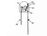
- FIG. 5 shows an example of a bullet-type light emitting device.
- the semiconductor light emitting element 51 is mounted on the lead 50 ′ via the mount material 52 and covered with the pre-dip material 54.
- a lead 50 is connected to the semiconductor light emitting element 51 by a wire 53 and is enclosed by a casting material 55.
- the pre-dip material 54 contains the phosphor according to the embodiment.
- the light emitting device according to the embodiment for example, the white LED is used not only for general illumination, but also as a light emitting device used in combination with a filter such as a color filter and the light emitting device, for example, a light source for a liquid crystal backlight. Is also optimal. Specifically, it can also be used as a red light emitting material for an inorganic electroluminescent device using a liquid crystal backlight source or a blue light emitting layer.
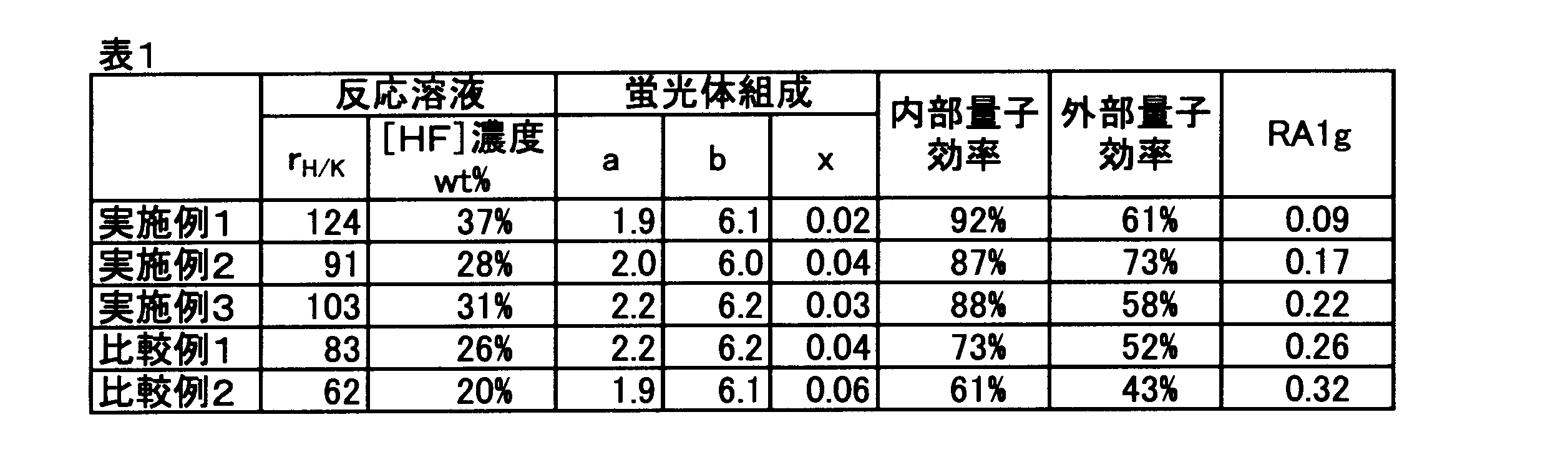
- Examples 1 to 3 A commercially available Si single crystal was prepared as a raw material. Further, 10.8 g of KMnO 4 powder, 250 ml of HF aqueous solution (49% by mass), and 150 ml of pure water were sufficiently mixed to obtain a reaction solution. The molar ratio of hydrogen fluoride to potassium permanganate in this reaction solution is 103, and the concentration of hydrogen fluoride [HF] is 31.5% by mass. Was allowed to react for 40 minutes. At this time, the reaction solution was stirred slowly to make the reaction solution uniform. As a result, a phosphor was formed on the surface of the Si single crystal, and the phosphor particles grown and enlarged were separated from the surface of the Si single crystal and deposited on the bottom of the container.
- the Raman spectrum of the obtained phosphor was measured, and R A1g was calculated. Furthermore, the internal quantum efficiency and the external quantum efficiency were measured with a C9920-02G type absolute PL quantum yield measuring apparatus (trade name, manufactured by Hamamatsu Photonics Co., Ltd.).
- the phosphors of Examples 2 and 3 and Comparative Examples 1 and 2 were prepared by changing the mixing ratio of the raw materials, and R A1g , internal quantum efficiency, and external quantum efficiency were similarly determined. The obtained results were as shown in Table 1 and FIGS.
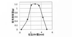
- Examples 4 to 5 and Comparative Examples 3 to 7 Using KMnO 4 powder and an aqueous HF solution, the mixing ratio was changed to prepare reaction solutions shown in Table 2, and a phosphor was prepared in the same manner as in Example 1.
- Table 2 also shows the internal quantum efficiency, the external quantum efficiency, and the phosphor yield of the obtained phosphor.
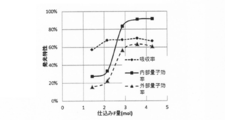
- FIGS. 6 and 7 show the relationship between the absorption rate, the internal quantum efficiency, and the external quantum efficiency with respect to the [HF] concentration, and the phosphor yield with respect to the [HF] concentration.
- DESCRIPTION OF SYMBOLS 100 ... Lead; 101 ... Lead; 102 ... Stem; 103 ... Semiconductor light-emitting device; DESCRIPTION OF SYMBOLS 104 ... Reflecting surface; 105 ... Phosphor layer 50, 50 '... Lead; 51 ... Semiconductor light emitting element; 52 ... Mounting material 53 ... Bonding wire; 54 ... Pre-dip material;
Landscapes
- Chemical & Material Sciences (AREA)
- Inorganic Chemistry (AREA)
- Engineering & Computer Science (AREA)
- Materials Engineering (AREA)
- Organic Chemistry (AREA)
- Luminescent Compositions (AREA)
- Led Device Packages (AREA)
Abstract
[課題]発光効率の高い赤色発光蛍光体と発光デバイス、蛍光体製造方法の提供。 [解決手段]基本組成が式:Ka(Si1-x,Mnx)Fbで表わされる蛍光体であって、この蛍光体のラマンスペクトルを測定した場合に、ラマンシフトが650±10cm-1の範囲に現れる、結晶中のSi-F結合に帰属されるピークの強度に対する、ラマンシフトが600±10cm-1の範囲に現れる結晶中のMn-F結合に帰属されるピークの強度の比が0.09以上0.22以下であることを特徴とする赤色発光蛍光体。この蛍光体は、過マンガン酸カリウムに対するフッ化水素のモル比が87以上127以下である反応溶液をケイ素源に接触させることで製造することができる。
Description
本発明は、蛍光体、およびその製造方法、ならびにその蛍光体を用いた発光装置に関するものである。
発光ダイオード(Light-emitting Diode:LED)発光装置は、主に励起光源としてのLEDチップと蛍光体との組み合わせから構成され、その組み合わせによって様々な色の発光色を実現することができる。
白色光を放出する白色LED発光装置には、青色領域の光を放出するLEDチップと蛍光体との組み合わせが用いられている。例えば、青色光を放つLEDチップと、蛍光体混合物との組み合わせが挙げられる。蛍光体としては主に青色の補色である黄色発光蛍光体が使用され、擬似白色光LED発光装置として使用されている。その他にも青色光を放つLEDチップと、緑色ないし黄色発光蛍光体、および赤色発光蛍光体が用いられている3波長型白色LEDが開発されている。このような発光装置に用いられる赤色発光蛍光体の一つとしてK2SiF6:Mn蛍光体が知られている。
J.Electrochem.Soc.158(6)J179-183(2011)
本発明は、青色領域に発光ピークを有する光で励起されて発光する赤色発光蛍光体、およびかかる蛍光体の製造方法、ならびにかかる蛍光体を用いた発光装置を提供することを目的とするものである。
本発明の一実施態様にかかる赤色発光蛍光体は、基本組成が下記式(A):
Ka(Si1-x,Mnx)Fb (A)
(式中、1.5≦a≦2.5, 5.5≦b≦6.5, 0<x≦0.06である)
で表わされる赤色発光蛍光体であって、この蛍光体のラマンスペクトルを測定した場合に、ラマンシフトが650±10cm-1の範囲に現れる、結晶中のSi-F結合に帰属されるピークの強度に対する、ラマンシフトが600±10cm-1の範囲に現れる結晶中のMn-F結合に帰属されるピークの強度の比が0.09以上0.22以下であることを特徴とするものである。
Ka(Si1-x,Mnx)Fb (A)
(式中、1.5≦a≦2.5, 5.5≦b≦6.5, 0<x≦0.06である)
で表わされる赤色発光蛍光体であって、この蛍光体のラマンスペクトルを測定した場合に、ラマンシフトが650±10cm-1の範囲に現れる、結晶中のSi-F結合に帰属されるピークの強度に対する、ラマンシフトが600±10cm-1の範囲に現れる結晶中のMn-F結合に帰属されるピークの強度の比が0.09以上0.22以下であることを特徴とするものである。
本発明の一実施態様にかかる蛍光体の製造方法は、反応溶液として過マンガン酸カリウムおよびフッ化水素を含有する水溶液を準備し、前記反応溶液中にケイ素源を浸漬して反応させることを含んでなる蛍光体の製造方法であって、前記反応溶液中の過マンガン酸カリウムに対するフッ化水素のモル比が87以上127以下であることを特徴とするものである。
本発明の一実施形態にかかる発光装置は、440nm以上470nm以下の波長領域の光を発光する発光素子と、前記蛍光体を含有する蛍光体層とを具備するものであることを特徴とするものである。
以下、本発明の実施の形態について、詳細に説明する。以下に示す実施形態は、本発明の技術思想を具体化するための蛍光体および発光装置を示すものであり、本発明は以下の例示に限定されない。
また、本明細書は特許請求の範囲に示される部材を、記載した実施形態に特定するものではない。特に実施形態に記載されている構成部品の大きさ、材質、形状、その配置等は本発明の範囲を限定する趣旨ではなく、説明例に過ぎない。なお、各図面が示す部材の大きさや位置関係等においても説明を明確にするため誇張していることがある。さらに、同一の名称、符号については同一、もしくは同質の部材を示しており、詳細な説明を省略する。本発明を構成する各要素は、複数の要素を同一の部材で構成して、同一の部材で複数の要素を兼用してもよく、逆に同一の部材の機能を複数の部材で分担して実現することも可能である。
本発明者らは、主としてケイフッ化カリウムからなり、マンガンで付活された蛍光体について鋭意検討および研究を重ねた結果、蛍光体のラマンスペクトルによって、結晶中の各結合に帰属するピークの強度と、蛍光体の発光特性とに相関関係があることを見出した。特に、マンガン付活されたケイフッ化カリウムからなる蛍光体に含まれるSi-F結合に帰属されるピークの強度とMn-F結合に帰属されるピークの強度の比が特定の範囲にあるときに、優れた発光特性が得られることを見出した。
実施形態にかかる赤色発光蛍光体は、主としてケイフッ化カリウムからなり、マンガンで付活された蛍光体である。ここで主としてケイフッ化カリウムからなる蛍光体とは、蛍光体の基本的な結晶構造がケイフッ化カリウムであり、結晶を構成する元素の一部が他の元素で置換されたものをいう。実施形態にかかる蛍光体の組成は下記式(A)式で表わされる。
Ka(Si1-x,Mnx)Fb (A)
式中
1.5≦a≦2.5、好ましくは1.8≦a≦2.2、
5.5≦b≦6.5、好ましくは5.7≦b≦6.2かつ
0<x≦0.06、好ましくは0.01≦x≦0.05
である。
Ka(Si1-x,Mnx)Fb (A)
式中
1.5≦a≦2.5、好ましくは1.8≦a≦2.2、
5.5≦b≦6.5、好ましくは5.7≦b≦6.2かつ
0<x≦0.06、好ましくは0.01≦x≦0.05
である。
実施形態にかかる蛍光体は、付活剤としてマンガンを含有するものである。マンガンが含有されていない場合(x=0)には紫外から青色領域に発光ピークを有する光で励起しても発光を確認することはできない。したがって、前記式(A)におけるxは0より大きいことが必要である。また、マンガンの含有量が多くなると発光効率が改良される傾向にあり、0.01以上であることが好ましい。また、赤色発光の蛍光体を得るためにはマンガンの価数は+4価であることが好ましい。
しかし、マンガンの含有量が多すぎる場合には、濃度消光現象が生じて、蛍光体の発光強度が弱くなる傾向にある。こうした不都合を避けるために、マンガンの含有量(x)は一般に0.06以下であり、0.05以下であることが好ましい。
蛍光体全体に対する各元素の含有量を分析するには、例えば以下のような方法が挙げられる。K、Si、Mnなどの金属元素は、合成された蛍光体をアルカリ融解し、例えばIRIS Advantage型ICP発光分光分析装置(商品名、サーモフィッシャーサイエンティフィック社製)によりICP発光分光法にて分析することができる。また、非金属元素Fは合成された蛍光体を熱加水分解により分離し、例えばDX-120型イオンクロマトグラフ分析装置(商品名、日本ダイオネクス株式会社製)により分析することができる。また、Fの分析は上述した金属元素と同様にアルカリ融解した後に、イオンクロマトグラフ法にて分析を行うことも可能である。
なお、実施形態による蛍光体は、化学量論的には酸素を含まないものである。しかしながら、蛍光体の合成プロセス中、または合成後の蛍光体表面の分解等により、酸素が不可避的に蛍光体中に混入してしまうことがある。蛍光体中の酸素の含有量はゼロであることが望ましいが、[酸素含有量]/[(フッ素含有量)+(酸素含有量)]の値が0.05より小さい範囲であれば、発光効率が大きく損なわれることがないので好ましい。
また、実施形態による蛍光体はNa、Rb、Csなどのアルカリ金属元素やTi、Ge、Snなどその他の元素を少量含有してもよい。これら元素が少量含有される場合であっても蛍光体は類似の発光スペクトルを示し、所望の効果を達成することができる。ただし、蛍光体の安定性、蛍光体合成時の反応性などの観点から、これらの元素の含有量は少ないことが好ましい。また、これらの元素を含む蛍光体を合成しようとすると、合成手順を変更する必要がある場合もあり、製造コストを抑制するために、式(A)に含まれる金属元素以外の金属元素を用いないことが好ましい。
実施形態による式(A)の蛍光体組成は、蛍光体を融解、または分解して分析することにより求めることができる。本発明者等の検討によれば、実施形態による蛍光体には、蛍光体内部に存在し、フッ素と結合して発光に寄与するマンガンと、蛍光体表面などで酸素と結合した形態で存在し、発光を阻害するマンガンとが存在することを見出した。つまり、ICP発光分光分析では蛍光体に含まれるMnの総量を測定することは可能であるが、その総量には発光を阻害するMnも含まれているという不都合が生じることになる。なお、ここで蛍光体の「表面」とは、現実の表面からXPS分析により検出可能な深さまでの範囲を含み、「内部」とはそれよりも内側の部分をいう。
フッ素と結合したマンガンはラマンスペクトル測定により検出することができる。ラマンスペクトル測定はサンプルに光を照射して散乱する光を測定することにより、サンプル固有の分子構造や結晶構造を調べる方法である。具体的には、蛍光体に光を照射して、その散乱光を測定する。この散乱光には、レイリー散乱光のほかに、結晶構造中に存在する各種の原子結合に対応して、照射された光とは波長が異なったラマン散乱光が含まれる。
そのため、散乱光を分析することで、サンプルとなる蛍光体に含まれるSi-F結合やMn-F結合に帰属されるピークをそれぞれ検出することが可能である。
そのため、散乱光を分析することで、サンプルとなる蛍光体に含まれるSi-F結合やMn-F結合に帰属されるピークをそれぞれ検出することが可能である。
具体的には、ラマンスペクトル測定は、LabRAM HR-PL装置(商品名、ホリバ・ジョバンイボン社製)等によって測定することができる。測定条件は、測定対象とする蛍光体の種類や粒子形状などによって変動し得るが、例えば以下の条件で測定することができる。
分析手法:後方散乱ラマンスペクトル測定、スリット幅:100μm、
光源:半導体レーザー(785nm)、光学系:顕微(体物100倍)、
ビーム径:1μm、光源出力:15mW
検出器:CCDマルチチャンネル
積算時間:120秒、積算回数:3回
試料条件:室温、大気中
分析手法:後方散乱ラマンスペクトル測定、スリット幅:100μm、
光源:半導体レーザー(785nm)、光学系:顕微(体物100倍)、
ビーム径:1μm、光源出力:15mW
検出器:CCDマルチチャンネル
積算時間:120秒、積算回数:3回
試料条件:室温、大気中
実施形態による蛍光体をラマンスペクトル測定すると、Si-F結合(SiF6
2-)に起因した3種類のピークと、Mn-F結合(MnF6
2-)に起因した3種類のピークが確認される。図1に実施形態による蛍光体のラマンスペクトルとそのピークの帰属を示す。
本発明者等は、組成が式(A)で表わされる蛍光体のうち、上記ラマンスペクトルで検出されたピークのうち、ラマンシフトが650±10cm-1の範囲に現れるSi-F結合に対応するピークの強度(I0)に対する、ラマンシフトが600±10cm-1の範囲に現れるMn-F結合に対応するピークの強度(I1)の比(I1/I0)が0.09以上0.22以下である蛍光体は外部量子効率及び内部量子効率が高くなることを見出した。具体的には、実施形態による蛍光体においては、内部量子効率は80%以上となる。
非特許文献1によると、ラマンシフトが650±10cm-1の範囲、およびに600±10cm-1の範囲現れるピークは、それぞれSi-F結合及びMn-F結合の伸縮振動であるA1gモードに帰属されている。すなわちこれらの2つのピークは同じ振動モードであるため、ピーク強度を比較することによって、Si-F結合とMn-F結合との存在比に対応し、大きいほどF原子と結合したMn原子が多いと考えることができる。以下、このピーク強度比をRA1gという。
非特許文献1では、480±10cm-1の範囲に現れるSi-F結合に帰属されるピーク、及び520±10cm-1の範囲に現れるMn-F結合に帰属されるピークは共にEgモードに帰属し、410±10cm-1の範囲に現れるSi-F結合に帰属されるピーク及び310±10cm-1の範囲に現れるMn-F結合に帰属されるピークは共にF2g(T2g)モードに帰属されている。これらEgモード、及びF2g(T2g)モードに帰属されるピーク強度から求められる比率REgおよびRF2gについて評価したところ、
それぞれ、0.75~1.5、および0.31~0.61の範囲である蛍光体は、外部量子効率及び内部量子効率が高い傾向が見出された。なお、Mn-F結合に対応するピークの強度がゼロの場合は、蛍光体中にMn-F結合が存在しないこととなり、Mnによる付活効果が認められず、蛍光体の発光を確認することができなくなる。
それぞれ、0.75~1.5、および0.31~0.61の範囲である蛍光体は、外部量子効率及び内部量子効率が高い傾向が見出された。なお、Mn-F結合に対応するピークの強度がゼロの場合は、蛍光体中にMn-F結合が存在しないこととなり、Mnによる付活効果が認められず、蛍光体の発光を確認することができなくなる。
組成が式(A)で表わされる蛍光体中のMnの総量は上述した通り、ICP発光分光法にて定量的に求めることが可能であるが、主としてケイフッ素化カリウムからなる蛍光体の一般的な合成方法では、蛍光体表面などに酸素と結合したMn、すなわちMnOxを含有することが多く、ICP発光分光法にて発光に関連するMnのみを検出することは困難である。一方、ラマンスペクトルでは定量的にMn量を求めることができないが、発光に直接関連するMn-F結合をSi-F結合の強度比として求めることができる。
ここで外部量子効率ηとは以下で規定する吸収率αと内部量子効率η’を乗じて算出した値である。

式中
E(λ):蛍光体へ照射した励起光源の全スペクトル(フォトン数換算)
R(λ):蛍光体の励起光源反射光スペクトル(フォトン数換算)
P(λ):蛍光体の発光スペクトル(フォトン数換算)
である。
E(λ):蛍光体へ照射した励起光源の全スペクトル(フォトン数換算)
R(λ):蛍光体の励起光源反射光スペクトル(フォトン数換算)
P(λ):蛍光体の発光スペクトル(フォトン数換算)
である。
つまり外部量子効率(η)は(I)×(II)によって算出可能である。
外部量子効率、内部量子効率、吸収率は例えばC9920-02G型絶対PL量子収率測定装置(商品名、浜松ホトニクス株式会社製)により測定することができる。上記発光特性を測定する際の励起光としてはピーク波長が440~460nm付近、半値幅5~15nmの青色光を使用することができる。
ラマンスペクトルから求められたRA1gと内部量子効率との関係、およびRA1gと外部量子効率との関係は図2および3に示す通りである(詳細後述)。RA1gが0.09以上0.22以下の範囲で、内部量子効率、外部量子効率ともに良好であることが分かる。
実施形態にかかる蛍光体は、任意の方法で製造することができるが、具体的には以下の方法により製造することができる。
まず、反応溶液として過マンガン酸カリウムおよびフッ化水素を含有する水溶液を準備する。そして、この反応溶液をケイ素源に接触させることで、そのケイ素源の表面において反応が進行して蛍光体が形成される。本発明において、この反応溶液は、過マンガン酸カリウムに対するフッ化水素のモル比(以下rH/Kという)は87以上(計算間違いがあったので、数値を訂正しました。明細書中の数字は訂正したつもりです。)127以下であり、90以上、および/または120以下であることが好ましい。また、反応溶液中のフッ化水素の濃度[HF]が27質量%以上40質量%以下であることが好ましく、28質量%以上35質量%以下であることがより好ましい。反応溶液における過マンガン酸カリウムに対するフッ化水素の比およびフッ化水素の濃度がこの範囲にあることで、内部量子効率の高い蛍光体が得られる。
反応溶液における過マンガン酸カリウムに対するフッ化水素の比rH/Kおよびフッ化水素の濃度がこの範囲にある場合に内部量子効率が良好な蛍光体が得られる明確な理由は良く分かっていないが、現在のところ以下のように考えられている。
本発明の一実施態様にかかる蛍光体はKaSiFb母体中のSi位置の一部をMnが置換している結晶構造を有している。過マンガン酸カリウムおよびフッ化水素を含む反応溶液にケイ素源を浸漬することにより蛍光体を合成する方法では、ケイ素源が過マンガン酸カリウムによって酸化されてシリカに転換され、そのシリカがHFによりフッ素化され、さらにイオン交換反応によってKaSiFb母体が生成する。一方、過マンガン酸カリウムはケイ素源を酸化した後、4価のMnとなり、KaSiFb母体中に取り込まれる。この反応過程中でシリカからKaSiFbが生成される反応は非常に早い。一方、4価のMnの生成反応はKaSiFbの生成速度に比べて遅い。
ここで、KaSiFbの生成速度は反応溶液中のプロトン[H+]濃度と[K+]濃度の比に依存する。つまり、HF濃度が高くなるとシリカの溶解速度が促進され、KaSiFbの生成反応は早くなる。一方、Mnの価数変化の速度は変化しないため、HFの濃度が高すぎるとKaSiFb母体中に取り込まれるMn量が少なくなる。その結果蛍光体中のSi-F結合に対するMn-F結合の割合が減少すると考えられる。また、KMnO4の濃度が高すぎると、Mn-F結合の割合が多いとMn同士が相互作用し、濃度消光と呼ばれる効率低下を引き起こすこともある。このため、反応溶液における過マンガン酸カリウムに対するフッ化水素の比およびフッ化水素の濃度が特定の範囲にあることが必要となる。
また、反応溶液中に含まれるHFの濃度が高いと、KaSiFbの生成が促進されるので好ましいが過度に高いと、反応溶液中の[K+]濃度割合が減少するため、イオン交換反応が進みにくくなり、蛍光体の収量が著しく減少すると考えられる。
このようにして製造された蛍光体粒子の表面に、例えば防湿やデバイス作製時の塗付性向上のため、コーティング処理により表層を形成させることもできる。この表層を構成する材料としては、シリコーン樹脂、エポキシ樹脂、フッ素樹脂、テトラエトキシシラン(TEOS)、シリカ、ケイ酸亜鉛、ケイ酸アルミニウム、カルシウムポリフォスフェート、シリコーンオイル、およびシリコーングリースから選択される少なくとも一種からなるものを挙げることができる。ケイ酸亜鉛およびケイ酸アルミニウムは、例えばZnO・cSiO2(1≦c≦4)、及びAl2O3・dSiO2(1≦d≦10)でそれぞれ表わされる。表層は蛍光体粒子表面が完全に覆われている必要はなく、粒子表面の一部が露出していてもよい。蛍光体粒子の表面の一部に、上述したような材質からなる表層が存在していれば、表面全体が完全に被覆されていなくてもその効果が得られる。表層は、その分散液または溶液の中に蛍光体粒子を所定時間浸漬した後、加熱等により乾燥させることによって配置される。蛍光体としての本来の機能を損なうことなく、表層の効果を得るために、表層は、蛍光体粒子の0.1~5%の体積割合で存在することが好ましい。
また、実施形態による蛍光体は使用する発光装置への塗布方法に応じて分級することもできる。青色領域に発光ピークを有する励起光を使用した通常の白色LEDなどでは、一般的に1~50μmに分級された蛍光体粒子を用いることが好ましい。分級後の蛍光体の粒径が過度に小さいと、発光強度が低下してしまうことがある。また、粒径が過度に大きいとLEDに塗布する際、蛍光体層塗布装置に蛍光体が目詰まりし作業効率や歩留りの低下、出来上がった発光装置の色ムラの原因となることがある。
本発明の実施形態にかかる蛍光体は、青色の波長領域に発光ピークを有する発光素子と組み合わせて、実施形態にかかるLED発光装置を得ることができる。実施形態にかかるLED発光装置は、従来のK2SiF6:Mn赤色蛍光体を用いたLED発光装置より、発光強度が高い。
実施形態に係る蛍光体は紫外から青色領域に発光ピークを有する励起光源にて励起可能である。この蛍光体を発酵装置に用いる場合には、図5に示された実施形態による蛍光体の励起スペクトルからわかるように、440nm以上470nm以下の波長領域に発光ピークを有する発光素子を励起光源として利用することが望ましい。上述の波長範囲外に発光ピークを有する発光素子を用いることは、発光効率の観点からは好ましくない。発光素子としては、LEDチップやレーザーダイオードなどの固体光源素子を使用できる。
実施形態にかかる蛍光体は、赤色の発光をする蛍光体である。したがって、緑色発光蛍光体および黄色発光蛍光体と組み合わせて用いることにより、白色発光装置を得ることができる。使用する蛍光体は発光装置の目的に合わせて任意に選択することができる。例えば、色温度が低い白色発光装置を提供する際には、実施形態による蛍光体と黄色発光蛍光体と組み合わせることにより、効率と演色性を両立した発光装置を提供することができる。
緑色発光蛍光体および黄色発光蛍光体は、520nm以上570nm以下の波長領域に主発光ピークを有する蛍光体ということができる。このような蛍光体としては、例えば、(Sr,Ca,Ba)2SiO4:Eu、Ca3(Sc,Mg)2Si3O12:Ce等のケイ酸塩蛍光体、(Y,Gd)3(Al,Ga)5O12:Ce、(Ca,Sr,Ba)Ga2S4:Eu等の硫化物蛍光体、(Ca,Sr,Ba)Si2O2N2:Eu、(Ca,Sr)-αSiAlON等のアルカリ土類酸窒化物蛍光体などが挙げられる。なお、主発光ピークとは、発光スペクトルのピーク強度が最も大きくなる波長のことであり、例示された蛍光体の発光ピークは、これまで文献などで報告されている。なお、蛍光体作製時の少量の元素添加やわずかな組成変動により、10nm程度の発光ピークの変化が認められることがあるが、そのような蛍光体も前記の例示された蛍光体に包含されるものとする。
また、実施形態による蛍光体を用いた発光装置には、上記以外の、青緑色発光蛍光体、橙色発光蛍光体、赤色発光蛍光体も用途に応じて使用することができる。
橙色発光蛍光体、赤色発光蛍光体としては(Sr,Ca,Ba)2SiO4:Eu等のケイ酸塩蛍光体、Li(Eu,Sm)W2O8等のタングステン酸塩蛍光体、(La,Gd,Y)2O2S:Eu等の酸硫化物蛍光体、(Ca,Sr,Ba)S:Eu等の硫化物蛍光体、(Sr,Ba,Ca)2Si5N8:Eu、(Sr,Ca)AlSiN3:Eu等の窒化物蛍光体などが挙げられる。実施形態による蛍光体に更にこれらの蛍光体を組み合わせて使用することにより、効率だけでなく、照明用途での演色性や、バックライト用途での色域を更に改善することができる。ただし、使用する蛍光体の数が多すぎると、蛍光体同士が吸収、発光をする再吸収現象や蛍光体の発光が再度蛍光体に照射され、散乱現象が生じて、発光装置の効率が低下する。
図4には、本発明の一実施形態にかかる発光装置の断面を示す。
図示する発光装置は、発光装置はリード100およびリード101とステム102、半導体発光素子103、反射面104、蛍光体層105を有する。底面中央部には、半導体発光素子103がAgペースト等によりマウントされている。半導体発光素子103としては、紫外発光を行なうもの、あるいは可視領域の発光を行なうものを用いることができる。例えば、GaAs系、GaN系等の半導体発光ダイオード等を用いることが可能である。なお、リード100およびリード101の配置は、適宜変更することができる。
発光装置の凹部内には、蛍光体層105が配置される。この蛍光体層105は、実施形態にかかる蛍光体を、例えばシリコーン樹脂からなる樹脂層211中に5wt%以上50wt%以下の割合で分散することによって形成することができる。蛍光体は、有機材料である樹脂や無機材料であるガラスなど種々のバインダーによって、付着させることができる。
有機材料のバインダーとしては、上述したシリコーン樹脂の他にエポキシ樹脂、アクリル樹脂など耐光性に優れた透明樹脂が適している。無機材料のバインダーとしてはアルカリ土類ホウ酸塩等を使用した低融点ガラス等、粒径の大きな蛍光体を付着させるために超微粒子のシリカ、アルミナ等、沈殿法により得られるアルカリ土類リン酸塩等が適している。これらのバインダーは、単独でも2種以上を組み合わせて用いてもよい。
また、蛍光体層に使用される蛍光体には、必要に応じて表面にコーティング処理を施すことができる。この表面コーティングにより、蛍光体が熱、湿度、紫外線等の外的要因から劣化が防止される。さらに、蛍光体の分散性を調整することが可能となり、蛍光体層の設計を容易に行なうことができる。
また、蛍光体層に使用される蛍光体には、必要に応じて表面にコーティング処理を施すことができる。この表面コーティングにより、蛍光体が熱、湿度、紫外線等の外的要因から劣化が防止される。さらに、蛍光体の分散性を調整することが可能となり、蛍光体層の設計を容易に行なうことができる。
半導体発光素子103としては、n型電極とp型電極とを同一面上に有するフリップチップ型のものを用いることも可能である。この場合には、ワイヤの断線や剥離、ワイヤによる光吸収等のワイヤに起因した問題を解消して、信頼性の高い高輝度な半導体発光装置が得られる。また、半導体発光素子103にn型基板を用いて、次のような構成とすることもできる。具体的には、n型基板の裏面にn型電極を形成し、基板上の半導体層上面にはp型電極を形成して、n型電極またはp型電極をリードにマウントする。p型電極またはn型電極は、ワイヤにより他方のリードに接続することができる。半導体発光素子103のサイズ、凹部の寸法および形状は、適宜変更することができる。
図5には、砲弾型の発光装置の例を示す。半導体発光素子51は、リード50’にマウント材52を介して実装され、プレディップ材54で覆われる。ワイヤ53により、リード50が半導体発光素子51に接続され、キャスティング材55で封入されている。プレディップ材54中には、実施形態にかかる蛍光体が含有される。
上述したように、実施形態にかかる発光装置、例えば白色LEDは一般照明等だけでなく、カラーフィルターなどのフィルターと発光装置を組み合わせて使用される発光デバイス、例えば液晶用バックライト用の光源等としても最適である。具体的には、液晶のバックライト光源や青色発光層を使用した無機エレクトロルミネッセンス装置の赤色発光材料としても使用することができる。
上述したように、実施形態にかかる発光装置、例えば白色LEDは一般照明等だけでなく、カラーフィルターなどのフィルターと発光装置を組み合わせて使用される発光デバイス、例えば液晶用バックライト用の光源等としても最適である。具体的には、液晶のバックライト光源や青色発光層を使用した無機エレクトロルミネッセンス装置の赤色発光材料としても使用することができる。
以下、実施例および比較例を示して本発明をさらに詳細に説明するが、本発明はその趣旨を超えない限り、以下の実施例に限定されるものではない。
[実施例1~3]
原料として、市販のSi単結晶を準備した。また、KMnO4粉末10.8g、HF水溶液(49質量%)250ml、および純水150mlを十分混合し反応溶液とした。この反応溶液における過マンガン酸カリウムに対するフッ化水素のモル比は103であり、フッ化水素の濃度[HF]は31.5質量%である上記反応溶液中に室温(20℃)でSi単結晶を40分間反応させた。この際、反応溶液が均一になるようにゆっくり撹拌して反応させた。この結果、Si単結晶の表面に蛍光体が形成され、成長して大きくなった蛍光体粒子はSi単結晶表面から剥離して、容器底部に堆積した。
原料として、市販のSi単結晶を準備した。また、KMnO4粉末10.8g、HF水溶液(49質量%)250ml、および純水150mlを十分混合し反応溶液とした。この反応溶液における過マンガン酸カリウムに対するフッ化水素のモル比は103であり、フッ化水素の濃度[HF]は31.5質量%である上記反応溶液中に室温(20℃)でSi単結晶を40分間反応させた。この際、反応溶液が均一になるようにゆっくり撹拌して反応させた。この結果、Si単結晶の表面に蛍光体が形成され、成長して大きくなった蛍光体粒子はSi単結晶表面から剥離して、容器底部に堆積した。
得られた蛍光体のラマンスペクトルを測定し、RA1gを算出した。さらに内部量子効率および外部量子効率を、C9920-02G型絶対PL量子収率測定装置(商品名、浜松ホトニクス株式会社製)により測定した。
原料の配合比を変更して、実施例2および3、ならびに比較例1および2の蛍光体を調製し、同様にRA1g、内部量子効率、および外部量子効率を求めた。得られた結果は表1、図2および3に示す通りであった。
[実施例4~5および比較例3~7]
KMnO4粉末とHF水溶液とを用い、それらの配合比を変更して表2に示される反応溶液を調製し、それを用いて実施例1と同様の方法で蛍光体を調製した。得られた蛍光体の内部量子効率、外部量子効率、および蛍光体の収率も表2に合わせて示す。また、[HF]濃度に対する、吸収率、内部量子効率、および外部量子効率の変化、ならびに[HF]濃度に対する蛍光体収量の関係を図6および7に示す。
KMnO4粉末とHF水溶液とを用い、それらの配合比を変更して表2に示される反応溶液を調製し、それを用いて実施例1と同様の方法で蛍光体を調製した。得られた蛍光体の内部量子効率、外部量子効率、および蛍光体の収率も表2に合わせて示す。また、[HF]濃度に対する、吸収率、内部量子効率、および外部量子効率の変化、ならびに[HF]濃度に対する蛍光体収量の関係を図6および7に示す。

100…リード; 101…リード; 102…ステム; 103…半導体発光素子;
104…反射面; 105…蛍光体層
50、50’…リード; 51…半導体発光素子; 52…マウント材
53…ボンディングワイヤ; 54…プレディップ材; 55…キャスティング材。
104…反射面; 105…蛍光体層
50、50’…リード; 51…半導体発光素子; 52…マウント材
53…ボンディングワイヤ; 54…プレディップ材; 55…キャスティング材。
Claims (12)
- 基本組成が下記式(A):
Ka(Si1-x,Mnx)Fb (A)
(式中、1.5≦a≦2.5、5.5≦b≦6.5、かつ0<x≦0.06である)
で表わされる蛍光体であって、この蛍光体のラマンスペクトルを測定した場合に、ラマンシフトが650±10cm-1の範囲に現れる、結晶中のSi-F結合に帰属されるピークの強度(I0)に対する、ラマンシフトが600±10cm-1の範囲に現れる結晶中のMn-F結合に帰属されるピークの強度(I1)の比(I1/I0)が0.09以上0.22以下であることを特徴とする蛍光体。 - 前記蛍光体の内部量子効率が80%以上である、請求項1に記載の蛍光体。
- 過マンガン酸カリウムおよびフッ化水素を含有する反応溶液にケイ素源を接触させて反応させることを含んでなる蛍光体の製造方法であって、前記反応溶液中の過マンガン酸カリウムに対するフッ化水素のモル比が87以上127以下であることを特徴とする、方法。
- 前記反応溶液中のフッ化水素濃度が、27~40質量%以下である、請求項3に記載の方法。
- ケイ素源が、単結晶シリコン、多結晶シリコン、非晶質シリコン、結晶性二酸化ケイ素および非晶質二酸化ケイ素からなる群から選択される、請求項3または4に記載の方法。
- ケイ素源がシリコン基板である、請求項3~5のいずれか1項に記載の方法。
- 440nm以上470nm以下の波長領域の光を発光する発光素子と、請求項1または2に記載の蛍光体を含む蛍光体層を具備することを特徴とする発光装置。
- 前記発光層は、520nm以上570nm以下の波長領域に主発光ピークを有する蛍光体を含むことを特徴とする請求項7に記載の発光装置。
- 前記蛍光体層が、緑色発光蛍光体または黄色発光蛍光体をさらに含む、請求項7または8に記載の発光装置。
- 前記の緑色発光蛍光体または黄色発光蛍光体が、(Sr,Ca,Ba)2SiO4:Eu、Ca3(Sc,Mg)2Si3O12:Ce、(Y,Gd)3(Al,Ga)5O12:Ce、(Ca,Sr,Ba)Ga2S4:Eu、(Ca,Sr,Ba)Si2O2N2:Eu、および(Ca,Sr)-αSiAlONからなる群から選択される、請求項9に記載の発光装置。
- 前記蛍光体層が、橙色発光蛍光体または赤色発光蛍光体をさらに含む、請求項7~10のいずれか1項に記載の発光装置。
- 前記の橙色発光蛍光体または赤色発光蛍光体が、(Sr,Ca,Ba)2SiO4:Eu、Li(Eu,Sm)W2O8、(La,Gd,Y)2O2S:Eu、(Ca,Sr,Ba)S:Eu、(Sr,Ba,Ca)2Si5N8:Eu、および(Sr,Ca)AlSiN3:Euからなる群から選択されるものである、請求項11に記載の発光装置。
Priority Applications (4)
| Application Number | Priority Date | Filing Date | Title |
|---|---|---|---|
| KR1020167017423A KR20160092003A (ko) | 2013-12-09 | 2014-12-09 | 형광체, 그의 제조 방법, 및 상기 형광체를 사용한 발광 장치 |
| KR1020177036905A KR101940439B1 (ko) | 2013-12-09 | 2014-12-09 | 형광체 및 그의 제조 방법, 및 상기 형광체를 포함하는 발광 장치 |
| CN201480065679.0A CN105793388A (zh) | 2013-12-09 | 2014-12-09 | 荧光体及其制造方法、以及使用了该荧光体的发光装置 |
| US15/175,627 US10519368B2 (en) | 2013-12-09 | 2016-06-07 | Phosphor, manufacturing method thereof, and light-emitting device using the phosphor |
Applications Claiming Priority (2)
| Application Number | Priority Date | Filing Date | Title |
|---|---|---|---|
| JP2013254437A JP6342146B2 (ja) | 2013-12-09 | 2013-12-09 | 蛍光体、およびその製造方法、ならびにその蛍光体を用いた発光装置 |
| JP2013-254437 | 2013-12-09 |
Related Child Applications (1)
| Application Number | Title | Priority Date | Filing Date |
|---|---|---|---|
| US15/175,627 Continuation US10519368B2 (en) | 2013-12-09 | 2016-06-07 | Phosphor, manufacturing method thereof, and light-emitting device using the phosphor |
Publications (1)
| Publication Number | Publication Date |
|---|---|
| WO2015087861A1 true WO2015087861A1 (ja) | 2015-06-18 |
Family
ID=53371163
Family Applications (1)
| Application Number | Title | Priority Date | Filing Date |
|---|---|---|---|
| PCT/JP2014/082516 Ceased WO2015087861A1 (ja) | 2013-12-09 | 2014-12-09 | 蛍光体、およびその製造方法、ならびにその蛍光体を用いた発光装置 |
Country Status (6)
| Country | Link |
|---|---|
| US (1) | US10519368B2 (ja) |
| JP (1) | JP6342146B2 (ja) |
| KR (2) | KR20160092003A (ja) |
| CN (2) | CN112500855A (ja) |
| TW (1) | TWI529978B (ja) |
| WO (1) | WO2015087861A1 (ja) |
Cited By (1)
| Publication number | Priority date | Publication date | Assignee | Title |
|---|---|---|---|---|
| US9944848B2 (en) | 2014-09-30 | 2018-04-17 | Nichia Corporation | Fluoride fluorescent material, method for producing the same, and light emitting device |
Families Citing this family (9)
| Publication number | Priority date | Publication date | Assignee | Title |
|---|---|---|---|---|
| JP2016088950A (ja) * | 2014-10-30 | 2016-05-23 | 信越化学工業株式会社 | 赤色蛍光体 |
| CN105181671B (zh) * | 2015-09-21 | 2018-06-26 | 中国科学院长春光学精密机械与物理研究所 | 测试氮化物荧光粉老化程度的方法 |
| CN105331360A (zh) * | 2015-10-30 | 2016-02-17 | 烟台希尔德新材料有限公司 | Led红色荧光粉及其组合物的产业化制备方法以及产品和应用 |
| JP2018002813A (ja) | 2016-06-29 | 2018-01-11 | 株式会社東芝 | 蛍光体および発光装置 |
| US9929321B2 (en) | 2016-08-04 | 2018-03-27 | Kabushiki Kaisha Toshiba | Phosphor, producing method thereof and light-emitting device employing the phosphor |
| JP6812231B2 (ja) * | 2016-12-20 | 2021-01-13 | デンカ株式会社 | フッ化物蛍光体の製造方法 |
| JP2019044017A (ja) * | 2017-08-30 | 2019-03-22 | デンカ株式会社 | フッ化物蛍光体及び発光装置 |
| JP2019044018A (ja) * | 2017-08-30 | 2019-03-22 | デンカ株式会社 | フッ化物蛍光体及び発光装置 |
| US10608148B2 (en) * | 2018-05-31 | 2020-03-31 | Cree, Inc. | Stabilized fluoride phosphor for light emitting diode (LED) applications |
Citations (4)
| Publication number | Priority date | Publication date | Assignee | Title |
|---|---|---|---|---|
| WO2009119486A1 (ja) * | 2008-03-25 | 2009-10-01 | 国立大学法人群馬大学 | 蛍光体及びその製造方法並びに該蛍光体を用いた白色発光ダイオード |
| JP2010209311A (ja) * | 2008-09-05 | 2010-09-24 | Mitsubishi Chemicals Corp | 蛍光体及びその製造方法と、その蛍光体を用いた蛍光体含有組成物及び発光装置、並びに、その発光装置を用いた画像表示装置及び照明装置 |
| JP2013014715A (ja) * | 2011-07-06 | 2013-01-24 | Nichia Corp | フッ化物蛍光体及びそのフッ化物蛍光体を用いた発光装置 |
| WO2013137144A1 (ja) * | 2012-03-15 | 2013-09-19 | 株式会社 東芝 | 白色照明装置 |
Family Cites Families (7)
| Publication number | Priority date | Publication date | Assignee | Title |
|---|---|---|---|---|
| US7497973B2 (en) | 2005-02-02 | 2009-03-03 | Lumination Llc | Red line emitting phosphor materials for use in LED applications |
| KR101592836B1 (ko) * | 2008-02-07 | 2016-02-05 | 미쓰비시 가가꾸 가부시키가이샤 | 반도체 발광 장치, 백라이트, 컬러 화상 표시 장치, 및 그들에 사용하는 형광체 |
| JP5105132B1 (ja) | 2011-06-02 | 2012-12-19 | 三菱化学株式会社 | 半導体発光装置、半導体発光システムおよび照明器具 |
| JP5512905B1 (ja) | 2011-12-16 | 2014-06-04 | コーニンクレッカ フィリップス エヌ ヴェ | Ledアプリケーションのためのマンガン活性化ヘキサフルオロケイ酸 |
| JP2014177511A (ja) | 2013-03-13 | 2014-09-25 | Toshiba Corp | 蛍光体、およびその製造方法、ならびにその蛍光体を用いた発光装置 |
| JP2014177586A (ja) * | 2013-03-15 | 2014-09-25 | Toshiba Corp | 蛍光体、およびその製造方法、ならびにその蛍光体を用いた発光装置 |
| CN103540314B (zh) * | 2013-10-10 | 2015-01-14 | 上海师范大学 | 一种低温合成的氟硅酸盐纳米棒红色荧光粉及其制备方法 |
-
2013
- 2013-12-09 JP JP2013254437A patent/JP6342146B2/ja active Active
-
2014
- 2014-12-08 TW TW103142609A patent/TWI529978B/zh active
- 2014-12-09 WO PCT/JP2014/082516 patent/WO2015087861A1/ja not_active Ceased
- 2014-12-09 KR KR1020167017423A patent/KR20160092003A/ko not_active Ceased
- 2014-12-09 KR KR1020177036905A patent/KR101940439B1/ko active Active
- 2014-12-09 CN CN202011484047.1A patent/CN112500855A/zh active Pending
- 2014-12-09 CN CN201480065679.0A patent/CN105793388A/zh active Pending
-
2016
- 2016-06-07 US US15/175,627 patent/US10519368B2/en active Active
Patent Citations (4)
| Publication number | Priority date | Publication date | Assignee | Title |
|---|---|---|---|---|
| WO2009119486A1 (ja) * | 2008-03-25 | 2009-10-01 | 国立大学法人群馬大学 | 蛍光体及びその製造方法並びに該蛍光体を用いた白色発光ダイオード |
| JP2010209311A (ja) * | 2008-09-05 | 2010-09-24 | Mitsubishi Chemicals Corp | 蛍光体及びその製造方法と、その蛍光体を用いた蛍光体含有組成物及び発光装置、並びに、その発光装置を用いた画像表示装置及び照明装置 |
| JP2013014715A (ja) * | 2011-07-06 | 2013-01-24 | Nichia Corp | フッ化物蛍光体及びそのフッ化物蛍光体を用いた発光装置 |
| WO2013137144A1 (ja) * | 2012-03-15 | 2013-09-19 | 株式会社 東芝 | 白色照明装置 |
Non-Patent Citations (1)
| Title |
|---|
| SADAO ADACHI ET AL.: "Direct synthesis and properties of K2SiF6:Mn4+ phosphor by wet chemical etching of Si wafer", JOURNAL OF APPLIED PHYSICS, vol. 104, 18 July 2008 (2008-07-18), pages 023512 * |
Cited By (2)
| Publication number | Priority date | Publication date | Assignee | Title |
|---|---|---|---|---|
| US9944848B2 (en) | 2014-09-30 | 2018-04-17 | Nichia Corporation | Fluoride fluorescent material, method for producing the same, and light emitting device |
| US10400166B2 (en) | 2014-09-30 | 2019-09-03 | Nichia Corporation | Fluoride fluorescent material and light emitting device |
Also Published As
| Publication number | Publication date |
|---|---|
| TWI529978B (zh) | 2016-04-11 |
| CN112500855A (zh) | 2021-03-16 |
| JP6342146B2 (ja) | 2018-06-13 |
| TW201530830A (zh) | 2015-08-01 |
| KR101940439B1 (ko) | 2019-01-18 |
| US10519368B2 (en) | 2019-12-31 |
| JP2015113362A (ja) | 2015-06-22 |
| KR20160092003A (ko) | 2016-08-03 |
| US20160340577A1 (en) | 2016-11-24 |
| KR20180002893A (ko) | 2018-01-08 |
| CN105793388A (zh) | 2016-07-20 |
Similar Documents
| Publication | Publication Date | Title |
|---|---|---|
| JP6342146B2 (ja) | 蛍光体、およびその製造方法、ならびにその蛍光体を用いた発光装置 | |
| JP5840540B2 (ja) | 白色照明装置 | |
| TWI650404B (zh) | 螢光體、及其製造方法以及使用該螢光體之發光裝置 | |
| JP6603458B2 (ja) | 蛍光体、およびその製造方法、ならびにその蛍光体を用いた発光装置 | |
| WO2014141851A1 (ja) | 蛍光体、およびその製造方法、ならびにその蛍光体を用いた発光装置 | |
| JP6486990B2 (ja) | 蛍光体、およびその製造方法、ならびにその蛍光体を用いた発光装置 | |
| JP5915801B1 (ja) | フッ化物蛍光体及びその製造方法並びに発光装置 | |
| WO2016136066A1 (ja) | フッ化物蛍光体複合体、およびその製造方法、ならびにその複合体を用いた発光装置 | |
| JP2018024870A (ja) | 蛍光体、及びその製造方法、並びにその蛍光体を用いた発光装置 | |
| JP6066003B2 (ja) | フッ化物蛍光体及びその製造方法並びに発光装置 | |
| TWI619799B (zh) | Phosphor, manufacturing method thereof, and illuminating device using the same | |
| US10032967B2 (en) | Phosphor and light-emitting device | |
| JP6344460B2 (ja) | フッ化物蛍光体の製造方法 | |
| JP2017052826A (ja) | 蛍光材料、およびその製造方法、ならびにその蛍光材料を用いた発光装置 |
Legal Events
| Date | Code | Title | Description |
|---|---|---|---|
| 121 | Ep: the epo has been informed by wipo that ep was designated in this application |
Ref document number: 14870458 Country of ref document: EP Kind code of ref document: A1 |
|
| NENP | Non-entry into the national phase |
Ref country code: DE |
|
| ENP | Entry into the national phase |
Ref document number: 20167017423 Country of ref document: KR Kind code of ref document: A |
|
| 122 | Ep: pct application non-entry in european phase |
Ref document number: 14870458 Country of ref document: EP Kind code of ref document: A1 |