WO2015083424A1 - 導電シート、静電容量式タッチパネル及び表示装置 - Google Patents
導電シート、静電容量式タッチパネル及び表示装置 Download PDFInfo
- Publication number
- WO2015083424A1 WO2015083424A1 PCT/JP2014/076305 JP2014076305W WO2015083424A1 WO 2015083424 A1 WO2015083424 A1 WO 2015083424A1 JP 2014076305 W JP2014076305 W JP 2014076305W WO 2015083424 A1 WO2015083424 A1 WO 2015083424A1
- Authority
- WO
- WIPO (PCT)
- Prior art keywords
- electrode
- upper electrode
- conductive sheet
- lower electrode
- mesh
- Prior art date
- Legal status (The legal status is an assumption and is not a legal conclusion. Google has not performed a legal analysis and makes no representation as to the accuracy of the status listed.)
- Ceased
Links
Images


Classifications
-
- G—PHYSICS
- G06—COMPUTING OR CALCULATING; COUNTING
- G06F—ELECTRIC DIGITAL DATA PROCESSING
- G06F3/00—Input arrangements for transferring data to be processed into a form capable of being handled by the computer; Output arrangements for transferring data from processing unit to output unit, e.g. interface arrangements
- G06F3/01—Input arrangements or combined input and output arrangements for interaction between user and computer
- G06F3/03—Arrangements for converting the position or the displacement of a member into a coded form
- G06F3/041—Digitisers, e.g. for touch screens or touch pads, characterised by the transducing means
- G06F3/044—Digitisers, e.g. for touch screens or touch pads, characterised by the transducing means by capacitive means
-
- G—PHYSICS
- G06—COMPUTING OR CALCULATING; COUNTING
- G06F—ELECTRIC DIGITAL DATA PROCESSING
- G06F3/00—Input arrangements for transferring data to be processed into a form capable of being handled by the computer; Output arrangements for transferring data from processing unit to output unit, e.g. interface arrangements
- G06F3/01—Input arrangements or combined input and output arrangements for interaction between user and computer
- G06F3/03—Arrangements for converting the position or the displacement of a member into a coded form
- G06F3/041—Digitisers, e.g. for touch screens or touch pads, characterised by the transducing means
- G06F3/044—Digitisers, e.g. for touch screens or touch pads, characterised by the transducing means by capacitive means
- G06F3/0445—Digitisers, e.g. for touch screens or touch pads, characterised by the transducing means by capacitive means using two or more layers of sensing electrodes, e.g. using two layers of electrodes separated by a dielectric layer
-
- G—PHYSICS
- G06—COMPUTING OR CALCULATING; COUNTING
- G06F—ELECTRIC DIGITAL DATA PROCESSING
- G06F3/00—Input arrangements for transferring data to be processed into a form capable of being handled by the computer; Output arrangements for transferring data from processing unit to output unit, e.g. interface arrangements
- G06F3/01—Input arrangements or combined input and output arrangements for interaction between user and computer
- G06F3/03—Arrangements for converting the position or the displacement of a member into a coded form
- G06F3/041—Digitisers, e.g. for touch screens or touch pads, characterised by the transducing means
- G06F3/044—Digitisers, e.g. for touch screens or touch pads, characterised by the transducing means by capacitive means
- G06F3/0446—Digitisers, e.g. for touch screens or touch pads, characterised by the transducing means by capacitive means using a grid-like structure of electrodes in at least two directions, e.g. using row and column electrodes
-
- G—PHYSICS
- G06—COMPUTING OR CALCULATING; COUNTING
- G06F—ELECTRIC DIGITAL DATA PROCESSING
- G06F3/00—Input arrangements for transferring data to be processed into a form capable of being handled by the computer; Output arrangements for transferring data from processing unit to output unit, e.g. interface arrangements
- G06F3/01—Input arrangements or combined input and output arrangements for interaction between user and computer
- G06F3/03—Arrangements for converting the position or the displacement of a member into a coded form
- G06F3/041—Digitisers, e.g. for touch screens or touch pads, characterised by the transducing means
- G06F3/044—Digitisers, e.g. for touch screens or touch pads, characterised by the transducing means by capacitive means
- G06F3/0447—Position sensing using the local deformation of sensor cells
-
- G—PHYSICS
- G06—COMPUTING OR CALCULATING; COUNTING
- G06F—ELECTRIC DIGITAL DATA PROCESSING
- G06F2203/00—Indexing scheme relating to G06F3/00 - G06F3/048
- G06F2203/041—Indexing scheme relating to G06F3/041 - G06F3/045
- G06F2203/04112—Electrode mesh in capacitive digitiser: electrode for touch sensing is formed of a mesh of very fine, normally metallic, interconnected lines that are almost invisible to see. This provides a quite large but transparent electrode surface, without need for ITO or similar transparent conductive material
Definitions
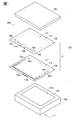
- FIG. 1 is an exploded perspective view of a main part of a display device 108 including a touch panel 100 according to the present embodiment.
- the touch panel 100 will be described first.
- the touch panel 100 includes a sensor body 102 and a control circuit (IC circuit or the like) (not shown).
- Examples of the first transparent substrate 14A and the second transparent substrate 14B include a plastic film, a plastic plate, and a glass plate.
- the space between the adjacent lower electrodes 18A is blank, but a dummy mesh may be disposed between the adjacent lower electrodes 18A to prevent the lower electrode 18A from being visually recognized.
- This dummy mesh preferably employs a cell having the same shape as the cell of the lower electrode formed on the same surface.
- Each lower electrode 18A is formed by intersecting thin wires 20A (metal wire rods) made of silver, copper, molybdenum, or an alloy containing one or more of them, or the like. Along with this intersection, a plurality of spaces (openings) surrounded by the thin wires 20A, that is, the second cells 22A are formed.
- thin wires 20A metal wire rods
- the second cells 22A are formed.
- the second cell 22A has, for example, a parallelogram shape, and typically has a rhombus shape in which the lengths of the four sides are equal as illustrated in FIG.
- the second cell 22A illustrated in FIG. 4 has two obtuse angles and two acute angles.
- the obtuse crossing angle ⁇ 1 in the diagonal relationship is the same angle greater than 90 °, and the acute crossing angle ⁇ 1 is the same angle less than 90 °.
- intersection angle ⁇ 1 which is an acute angle, is preferably 70 ° or less. In this case, it is effective in reducing moire. However, moire tends to occur even when ⁇ 1 is excessively small. In order to avoid this, ⁇ 1 is preferably in the range of 30 ° to 70 °, more preferably in the range of 45 ° to 70 °.
- the width direction dimension (line width W1) of the thin wire 20A is preferably 10 ⁇ m or less, and more preferably 5 ⁇ m or less.
- the moire and fine line appearance of the conductive pattern by the fine line 20A are improved, and the visibility is improved (that is, the fine line 20A forming the mesh is hardly seen).
- line 20A is 1 micrometer or more.
- the second cell 22A may be a random cell similarly to the first cell 22B, and is composed of another polygon such as a hexagon or a triangle. It may be a fixed pattern.
- the second cell 22A is preferably random or rhombus, and more preferably rhombus.
- the 2nd mesh electrode comprised from 22 A of cells may become an upper electrode, it may become a lower electrode, but when a rhombus cell is employ
- each lower electrode 18A is electrically connected to the first terminal wiring pattern 42a via the first connection portion 40a.
- the upper electrodes 18B formed on one main surface of the second transparent substrate 14B (see FIG. 3) constituting the second sheet body 10B are respectively in the second direction (x direction) as shown in FIG. A plurality of strip-shaped patterns extending.
- the plurality of upper electrodes 18B are arranged along the first direction (y direction). That is, in the laminated conductive sheet 12, as shown in FIG. 3, the lower electrode 18A and the upper electrode 18B face each other with the insulating second transparent base 14B interposed therebetween.
- Each upper electrode 18B is formed by the crossing of the thin wires 20B, similarly to the lower electrode 18A. Along with this intersection, a space (opening) surrounded by the thin wire 20B, that is, the first cell 22B is formed.
- the average cell pitch (hereinafter sometimes referred to as “Ps” as necessary) is preferably 50 to 400 ⁇ m, and more preferably 50 ⁇ m to 300 ⁇ m.
- the average cell pitch is defined by an average length obtained by measuring the maximum length of the first cell 22B in the direction in which the electrodes extend in any 30 cells.
- the width direction dimension (line width) of the thin wire 20B is not particularly limited, and can be set to 10 ⁇ m or less, for example, but preferably 5 ⁇ m or less. Combined with the random shape of the first cell 22B and the small width of the thin wire 20B, the moire is improved and the visibility is improved.
- the line width is more preferably 4 ⁇ m or less.
- line 20B is 1 micrometer or more.
- the average cell pitch Ps of the upper electrode 18B is preferably set to be larger than 50 ⁇ m and not more than 3200 ⁇ m and larger than the average cell pitch Pd of the lower electrode 18A.
- the average cell pitch Pd of the lower electrode 18A is the same as that of the upper electrode 18B.
- the maximum length of the second cell 22A in the direction in which the electrode extends is measured, and the length of any 30 second cells 22A is averaged. Defined as a calculated value.
- the average cell pitch Ps is greater than 1 and less than or equal to 8 times the average cell pitch Pd.
- the following relational expression holds between the average cell pitch Ps and the average cell pitch Pd. 1 ⁇ Ps / Pd ⁇ 8
- each upper electrode 18B is electrically connected to the second terminal wiring pattern 42b via the second connection portion 40b.
- Ws / Wd is 0.5. It can be set to 1.5 or less. That is, in this case, it is not essential to make the electrode width Ws of the upper electrode 18B located above smaller than the electrode width Wd of the lower electrode 18A located below, and in some cases, the electrode width Ws and the electrode width Wd Can be made the same, or the electrode width Ws can be made larger than the electrode width Wd. Of course, the electrode width Ws may be made smaller than the electrode width Wd.
- Ws / Wd is more preferably 0.8 or more and 1.2 or less. It is more preferable that the widths of the lower electrode 18A and the upper electrode 18B be approximately the same because the vertical sensitivity and the horizontal sensitivity with respect to the touch area become equal.
- the effective electrode area of the upper electrode 18B configured as described above is preferably 70% or more of the effective touch area. This makes it easier to increase the conductivity of the upper electrode 18B.
- the effective electrode area indicates the ratio of the area covered by the upper electrode 18B in the display region. Specifically, in FIG. 2, a value calculated by dividing the product of the electrode width Ws of the upper electrode 18B, the length in the y direction of the sensor unit 112, and the number of electrodes of the upper electrode 18B by the area of the sensor unit 112. is there. When a dummy electrode exists between the adjacent upper electrodes 18B, the dummy electrode is not included in the effective electrode area.
- the first sheet body 10 ⁇ / b> A applied to the touch panel 100 has the above-described many lower electrodes 18 ⁇ / b> A arranged in a portion corresponding to the sensor unit 112, and the terminal wiring unit 114 has each first connection unit.
- the first terminal wiring patterns 42a derived from 40a are arranged.
- a plurality of first terminals 116 a are provided in the central portion in the longitudinal direction on the peripheral portion on one long side (x direction) of the first sheet body 10 ⁇ / b> A.
- An array is formed in the length direction of one long side.
- a plurality of first connection portions 40a connected to the lower electrode 18A are arranged linearly along the short side (y direction) of the sensor portion 112.
- the first terminal wiring patterns 42a derived from the first connection portions 40a are routed through the terminal wiring portions 114 of the first sheet body 10A and are electrically connected to the corresponding first terminals 116a.
- the outer shape of the second sheet body 10B has a rectangular shape when viewed from above, and the outer shape of the sensor unit 112 also has a rectangular shape.
- a plurality of second terminals 116 b have a length of the one long side at a peripheral portion on one long side side (x direction) of the second sheet body 10 ⁇ / b> B in the center portion in the length direction.
- An array is formed in the vertical direction.
- a plurality of second connection portions 40b connected to the upper electrode 18B are arranged linearly along one long side of the sensor portion 112.
- the second terminal wiring pattern 42b derived from each second connection portion 40b is routed toward the substantially central portion of one long side of the second sheet body 10B, and is electrically connected to the corresponding second terminal 116b. It is connected.
- the derivation form of the first terminal wiring pattern 42a may be the same as the second terminal wiring pattern 42b described above. Conversely, the derivation form of the second terminal wiring pattern 42b is the same as the first terminal wiring pattern 42a described above. The same may be applied.
- FIG. 6 an example of a portion (overlapping portion) where the lower electrode 18A and the upper electrode 18B overlap is shown in FIG. 6 as a plan view.
- the thick solid line in FIG. 6 is the second cell 22A (small pitch) of the lower electrode 18A (standard mesh pattern), and the thin solid line is the first cell 22B (large pitch) of the upper electrode 18B (random mesh pattern).
- the protective layer 106 may be formed on the second sheet body 10B.
- the adhesive (OCA) 30 as an adhesive sheet is arrange
- the lower electrode 18A and the upper electrode 18B can be preferably formed by etching using a photolithography process, a microcontact printing patterning method, or a silver salt method in order to obtain a pattern having a narrow line width. In order to obtain a large number of patterns repeatedly, the silver salt method is more preferable.
- the microcontact printing patterning method is a method for obtaining a pattern having a narrow line width by using the microcontact printing method.
- the microcontact printing method is a method for producing a monomolecular film pattern by using an elastic polydimethylsiloxane stamp and bringing a thiol solution into contact with a gold base material as an ink (Whitedesed, Angew. Chem. Int. Ed., 1998, volume 37, page 550).
- a typical process of the microcontact printing patterning method is, for example, as follows. That is, first, the substrate is coated with a metal (eg, silver is sputter coated onto a PET substrate).
- a metal eg, silver is sputter coated onto a PET substrate.
- the masking of the monomolecular film is stamped using a microcontact printing method on a metal-coated substrate. Thereafter, the metal coated on the substrate is removed by etching except for the pattern under masking.
- a pattern of fine wires 20A and 20B having a mesh shape is obtained by exposing and developing a photosensitive material having a photosensitive silver salt-containing layer. Specific operations thereof are described in detail in paragraphs ⁇ 0163> to ⁇ 0241> of JP2009-4348A.
- the present invention is not particularly limited to the above-described embodiment, and various modifications can be made without departing from the gist of the present invention.
- the lower electrode 18A may be a random mesh pattern and the upper electrode 18B may be a regular mesh pattern
- an embodiment in which the lower electrode 18A is a regular mesh pattern and the upper electrode 18B is a random mesh pattern is most preferable.
- the random mesh randomly arranges the fine lines, so that useless line segments that contribute less to the conductivity than the standard pattern are generated.
- permeability to fall slightly compared with the regular mesh with the same electroconductivity. Therefore, it is most preferable to adopt a regular mesh pattern with less waste for the lower electrode having a small average cell pitch and a random mesh pattern for the upper electrode having a large average cell pitch.
- the average cell pitch Ps of the upper electrode 18B is larger than the average cell pitch Pd of the lower electrode 18A and is in the range of more than 1 and not more than 8 (preferably 2 to 6).
- the electrode widths Ws and Wd are constant (see FIG. 2). As shown in FIG. 7, for example, a part of the electrode width of the lower electrode 18A extends in the longitudinal direction. You may make it narrow on the way. In this case, a portion having a narrow electrode width may be disposed above the upper electrode 18B.
- the electrode width of a part of the lower electrode 18A may be reduced.
- the upper electrode 18B may be disposed above the portion where the electrode width is small.
- a part of the electrode width may be reduced while extending in the longitudinal direction, and the portions where the electrode width is reduced may be stacked.
- the initial value of the capacitance at the position where the lower electrode 18A and the upper electrode 18B face each other is reduced. Therefore, the S / N ratio can be improved.
- the narrow wire 20A forming the lower electrode 18A may be provided with a narrow portion or a disconnected portion at a location facing the upper electrode 18B.
- a part of the crossing point of the thin wire 20B forming the upper electrode 18B and the lower electrode 18A may be cut.
- the laminated conductive sheet 12 is formed by forming the lower electrode 18A on one main surface of the first transparent substrate 14A and forming the upper electrode 18B on one main surface of the second transparent substrate 14B (see FIGS. 2 and 2). 3)). That is, as shown in FIG. 8, even if the lower electrode 18A is formed on one main surface of the first transparent substrate 14A and the upper electrode 18B is formed on the other main surface of the first transparent substrate 14A. Good. In this case, the second transparent substrate 14B does not exist, the first transparent substrate 14A is laminated on the lower electrode 18A, and the upper electrode 18B is laminated on the first transparent substrate 14A.
- a part of the lower electrode and the upper electrode face each other.
- the average cell pitch Ps of the upper electrode was variously changed as shown in Table 1 below, and electrode stacks of Examples 1 to 7 and Comparative Examples 1 and 2 were configured. Thereafter, the amount of change in capacitance ( ⁇ Cm value) before and after the touch in each electrode laminate was determined. The larger the value of ⁇ Cm, the higher the possibility that a touch can be detected, and the better the detection accuracy.
- the reason why the peak decreases around Ps / Pd of 3 is that, as the average cell pitch Ps of the upper electrode increases, the lower electrode located near the center of the opening of the upper electrode is separated from the upper electrode. Since the distance increases, the influence of the electric field from the lower electrode on the upper electrode is reduced, so that the contribution to the ⁇ Cm value may be reduced. Therefore, it is not preferable that the average cell pitch Ps of the upper electrode is large, but has a preferable range.
- Table 1 also shows the moire evaluation of the electrode laminates of Examples 1 to 7 and Comparative Examples 1 and 2.
Landscapes
- Engineering & Computer Science (AREA)
- General Engineering & Computer Science (AREA)
- Theoretical Computer Science (AREA)
- Human Computer Interaction (AREA)
- Physics & Mathematics (AREA)
- General Physics & Mathematics (AREA)
- Position Input By Displaying (AREA)
Abstract
重ねて配置された2枚の金属メッシュからなる導電シートにおいて、該導電シートの透過率を高め、2枚の電極間に発生するモアレを抑制し、さらに、タッチパネルに使用した場合にタッチ検出の精度を高めることを課題とする。導電シート12には、第2シート体10B(絶縁層)を間に、下方電極18A、上方電極18Bが配置される。例えば、下方電極18Aは、複数個の第2セル22Aが連なることで形成されたメッシュパターンを呈し、一方、上方電極18Bは、形状が互いに異なる第1セル22Bを複数個含むランダムメッシュパターンを呈している。さらに、第1セル22Bの平均セルピッチPsは、第2セル22Aの平均セルピッチPdの1倍より大きく8倍以下に設定される。
Description
本発明は、導電シート、静電容量式タッチパネル及び表示装置に関する。
多機能携帯電話(スマートフォン)やデジタルカメラ等の表示装置として、指で触れることで様々な操作を行い得る、いわゆるタッチパネルが広汎に採用されるに至っている。これらの機器における表示装置は小型であるが、近時、パーソナルコンピュータ等の大型の表示装置にもタッチパネルが採用されつつある。特に、同時に複数箇所の検出が可能(マルチタッチ可能)な相互容量方式のタッチパネルが広く普及している。
タッチパネルにおける電極は、操作者が視認することが困難であること、及び導電性に優れていることが必要である。小型のタッチパネルでは、例えば、インジウム-スズ複合酸化物(ITO)電極が用いられることがあるが、大型のタッチパネルにITO電極を採用した場合、導電性が十分ではなく、また、コストの低廉化が困難である。
そこで、例えば、特許文献1に記載されるように、金属細線同士を交差させたセルが複数個連なることで網目模様(メッシュ)をなした電極を採用することが行われている。この場合、セルに開口が形成されるので電極が透光性を示すようになり、このために電極を視認することが困難である。また、金属細線からなるメッシュは導電性が高く、しかも、低コストで設けることができるという利点がある。
電極は、特許文献2に記載されるように、例えば、絶縁層の下方及び上方に配置されるように積層され、従って、下方電極と上方電極は、絶縁層を介して複数箇所で対向する。各々の対向箇所には静電容量が生じ、タッチパネルが指で押圧されると、静電容量が変化する。この際の変化量から、タッチパネルの如何なる部位が押圧されたのかが検出されるとともに、如何なる操作指令が発せられたのかが判断される。
また、特許文献2には、メッシュ電極を用いたタッチパネルにおいて、下方電極(特許文献2では「送信電極」)のセルピッチよりも、上方電極(特許文献2では「受信電極」)のセルピッチを大きくすることにより、検出精度を高めることができることが開示されている。
従来のITOを採用した相互容量方式のタッチパネルでは、下方電極(タッチパネルの1対の電極の中、タッチ面から遠い側の電極)の電極幅(長手方向に直交する方向)を大きくする一方で、上方電極(タッチパネルの1対の電極の中、タッチ面に近い側の電極)の電極幅を下方電極の幅に比して小さくすることでタッチ検出の精度を高めることが行われる場合がある。すなわち、下方電極からの電界は上方電極が形成されていない箇所を通過してくるので、上方電極の幅を小さくして通過する電界を増やしている。
金属メッシュからなる上方電極の電極幅を小さくする場合には、電極幅を小さくすると同時に電極を構成するメッシュの平均セルピッチを小さくすることが必要となる。しかしながら、この場合、セルの開口面積が小さくなることに伴って透過率が低くなるという問題が生じる。
また、上方電極の幅を小さくするために、上方電極をメッシュではなく線形状とすることも考えられるが、この場合、意図しない断線が生じると電極の導通が失われることになるため、歩留まりが悪化するという課題が生じる傾向がある。
そこで、特許文献2に記載されるように、上方電極のセルピッチを大きくして検出感度を高めることを検討したが、上方電極と下方電極のセルピッチの違いは、2つの電極間の周期的な干渉(モアレ)を生じ、メッシュの存在が容易に視認できるという致命的な課題が生じることが分かった。
本発明は上記した問題を解決するためになされたもので、金属メッシュからなる導電シートの透過率を高くし、上方電極と下方電極間のモアレを抑止し、しかも、タッチ検出の精度を高めることができる導電シート、静電容量式タッチパネル及び表示装置を提供することを目的とする。
前記の目的は、以下の[1]の構成により達成される。
[1] 下方電極と上方電極とが、絶縁層を介して積層された導電シートにおいて、
下方電極又は上方電極の少なくともいずれか一方が、金属線材同士が交差することで形成される複数個の第1セルが連なった第1メッシュ電極からなり、複数個の第1セルの形状が互いに異なるランダムセルであって、且つ第1メッシュ電極は、第1の方向に沿って延在するとともに、第1の方向に対して直交する第2の方向に沿って複数個並列され、
上方電極又は下方電極の残余の一方が、金属線材同士が交差することで形成される複数個の第2セルが連なった第2メッシュ電極からなり、且つ第2メッシュ電極は、第2の方向に沿って延在するとともに、第1の方向に沿って複数個並列され、
下方電極の平均セルピッチをPd、上方電極の平均セルピッチをPsとするとき、Ps/Pdが1より大きく8以下であることを特徴とする導電シート。
下方電極又は上方電極の少なくともいずれか一方が、金属線材同士が交差することで形成される複数個の第1セルが連なった第1メッシュ電極からなり、複数個の第1セルの形状が互いに異なるランダムセルであって、且つ第1メッシュ電極は、第1の方向に沿って延在するとともに、第1の方向に対して直交する第2の方向に沿って複数個並列され、
上方電極又は下方電極の残余の一方が、金属線材同士が交差することで形成される複数個の第2セルが連なった第2メッシュ電極からなり、且つ第2メッシュ電極は、第2の方向に沿って延在するとともに、第1の方向に沿って複数個並列され、
下方電極の平均セルピッチをPd、上方電極の平均セルピッチをPsとするとき、Ps/Pdが1より大きく8以下であることを特徴とする導電シート。
下方電極又は上方電極の少なくともいずれか一方の電極のセルをランダムな形状のセルで構成する。さらに、下方電極の平均セルピッチPdと、上方電極の平均セルピッチPsを上記の関係となるように設計することにより、下方電極から発せられる電界が、上方電極のセルの開口部を容易に通るようになる。このため、必ずしも上方電極の電極幅(長手方向に対して直交する方向の寸法)を小さくすることなく、指による押圧の前後における静電容量の変化量を大きくすることができる。このため、タッチ検出の精度が向上する。
また、上方電極を、平均セルピッチが大きなメッシュとして形成するため、該上方電極の透過率を高めることができる。このとき、上方電極又は下方電極の少なくとも一方がランダムな形状のセルからなるメッシュを採用することで、上方電極と下方電極間の平均セルピッチの違いによるモアレの発生が抑制され、視認性の悪化を生じない。
[2] Ps/Pdは、2以上6以下であることが一層好ましい。この場合、タッチ検出時の静電容量の変化量がより大きくなるからである。
[3] 上方電極の有効電極面積は、タッチ有効面積の70%以上とすることが好ましい。これにより上方電極の有効面積が高まるので、上方電極の抵抗値を小さくできて好ましい。
[4] 下方電極の電極幅をWd、上方電極の電極をWsとするとき、Ws/Wdは、0.5以上1.5以下に設定することができる。Ws/Wdは、0.8以上1.2以下であることがより好ましい。なお、WsとWdを近い値に設定することで、表示装置内の縦方向の検出精度と横方向の検出精度を、補正を行うことなく近似させることができる。ここで、電極幅とは、下方電極及び上方電極において、それぞれ長手方向に直交する方向の寸法を指し、各電極の幅が変動する場合には、各々の平均幅で比較するものとする。
すなわち、本発明においては、従来技術のように、上方電極の電極幅Wsを下方電極の電極幅Wdに比して小さくする必要は必ずしもなく、同一としてもよいし、大きくするようにしてもよい。このため、上方電極の設計の自由度が向上する。
[5] 第2セルの形状の好適な例としては、菱形が挙げられる。
[6] 下方電極の平均セルピッチPdは、例えば、50μm以上400μm以下とすることができる。この場合、上方電極の平均セルピッチPsは、50μmより大きく3200μm以下とすればよい。
[7] ランダムパターンである第1メッシュ電極は、上方電極とすることが好ましい。勿論、この場合、第2セルを有する第2メッシュ電極が下方電極となる。
[8] 下方電極と上方電極の対向箇所で、下方電極又は上方電極の少なくともいずれか一方の電極幅を、他の部位(すなわち、対向箇所以外の部位)に比して小さく設定するようにしてもよい。例えば、上方電極のピッチを下方電極のピッチよりも大きくとると同時に上方電極の幅を大きくとった場合、上方電極と下方電極の対向面積が大きくなってしまう。この場合には、対向面積を調節するために対向部分のみ幅を狭めることで寄生容量を調節することが可能である。これにより、信号/ノイズ比(S/N比)の改善を図ることができる。
[9] 下方電極と上方電極の対向箇所の一部に、第1セルを形成する金属線材又は第2セルを形成する金属線材の少なくともいずれか一方が、線幅が小さくされているか、あるいは断線部とされていてもよい。上記したように上方電極のピッチを下方電極のピッチよりも大きくとると同時に上方電極の幅を大きくとった場合、上方電極と下方電極の対向面積が大きくなる。そこで、対向する箇所で対向面積を小さくする設計をすることで寄生容量を調節することが可能である。これにより、S/N比の改善を図ることができる。
[10] また、本発明は、上記のように構成された導電シートを有する静電容量式タッチパネルである。
[11] さらに、本発明は、上記の静電容量式タッチパネルを有する表示装置である。
本発明によれば、下方電極の平均セルピッチよりも上方電極の平均セルピッチを大きくし、且つ両平均セルピッチの比を1より大きく8以下とするようにしている。このような構成では、指による押圧の前後における静電容量の変化量を大きくすることができるので、タッチ検出の精度が向上し、透過率が向上する。また、下方電極又は上方電極の少なくとも一方をランダムセルからなるメッシュとしているので、平均セルピッチの比が1より大きく8以下の間の如何なる数値であってもモアレが十分に低減される。
以下、本発明に係る導電シート及び静電容量式タッチパネルにつき、これらを具備する表示装置との関係で好適な実施の形態を挙げ、添付の図面を参照して詳細に説明する。なお、本明細書において数値範囲を示す「~」は、その前後に記載される数値を下限値及び上限値として含む意味として使用される。
図1は、本実施の形態に係るタッチパネル100を含む表示装置108の要部分解斜視図である。タッチパネル100につき先ず説明すると、該タッチパネル100は、センサ本体102と、図示しない制御回路(IC回路等)とを有する。
センサ本体102は、第1シート体10Aと第2シート体10Bとが下方からこの順序で積層されて構成された積層導電シート(導電シート)12と、第2シート体10B上に積層された保護層106とを有する。すなわち、センサ本体102においては、下方から、第1シート体10A、第2シート体10B、保護層106が積層されている。
センサ本体102(積層導電シート12及び保護層106)は、表示装置108における表示パネル110上に配置され、例えば、液晶ディスプレイ等を構成する。センサ本体102は、上面から視認したときに、表示パネル110の表示画面110aに対応した領域に配されたタッチ位置のセンサ部112と、表示パネル110の外周部分に対応する領域に配された端子配線部114(いわゆる額縁)とを有する。
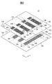
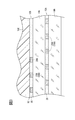
ここで、積層導電シート12につき、要部を拡大した図2及び図3を参照して説明する。
第1シート体10Aは、絶縁層である第1透明基体14Aの一主面上に形成された下方電極18Aを有する。第2シート体10Bも同様に、絶縁性の第2透明基体14Bの一主面上に形成された上方電極18Bを有する。図2及び図3では、導電膜の間に絶縁層として透明基体が配置される態様について説明しているが、導電膜同士を対向させた構成(絶縁層として透明接着剤が配置された構成)であってもよい。
下方電極18A、上方電極18Bの少なくともいずれか一方、又は双方が、ランダムなセルからなるメッシュであればよいが、一方がランダムなセルからなるメッシュであり、且つ残余の一方が互いに同様の形状(定型)のセルからなるメッシュであってもよい。本実施の形態では、下方電極18Aが定型のセルからなる第2メッシュ電極であり、上方電極18Bがランダムなセルからなる第1メッシュ電極である場合を説明する。なお、第2メッシュ電極である下方電極18Aを形成するセルを「第2セル」、第1メッシュ電極である上方電極18Bを形成するセルを「第1セル」と表記し、各々の参照符号を22A、22Bとする。
第1透明基体14A及び第2透明基体14Bの厚みは20~350μm以下が好ましく、30~250μmが一層好ましく、40~200μmが特に好ましい。
第1透明基体14A及び第2透明基体14Bとしては、プラスチックフイルム、プラスチック板、ガラス板等を挙げることができる。
上記プラスチックフイルム及びプラスチック板の原料としては、例えば、ポリエチレンテレフタレート(PET)、ポリエチレンナフタレート(PEN)等のポリエステル類;ポリエチレン(PE)、ポリプロピレン(PP)、ポリスチレン、ポリエチレンビニルアセテート(EVA)等のポリオレフィン類;ビニル系樹脂;その他、ポリカーボネート(PC)、ポリアミド、ポリイミド、アクリル樹脂、トリアセチルセルロース(TAC)、シクロオレフィンポリマー(COP)等を用いることができる。第1透明基体14A及び第2透明基体14Bの透過率は、85%以上であることが好ましい。
本実施の形態の場合、下方電極18Aは、図2に示すように、それぞれ第1方向(y方向/長手方向)に延びる複数の帯状のパターンを有する。下方電極18Aは、第2方向(第1方向と直交する方向:x方向)に向かう所定の幅方向寸法(電極幅Wd)を有するとともに、複数個が該x方向に沿って並列配置されている。
なお、図2では、隣接する下方電極18A同士の間を空白としているが、下方電極18Aが視認されることを防止するために、隣接する下方電極18A同士の間にダミーメッシュを配置することが好ましい。このダミーメッシュは、同一面上に形成される下方電極のセルと同じ形状のセルを採用することが好ましい。
各下方電極18Aは、銀、銅、モリブデン、又はこれらの中の1種以上を含む合金等からなる細線20A(金属線材)同士が交差することにより形成される。この交差に伴って、細線20Aによって囲繞される空間(開口部)、すなわち、第2セル22Aが複数個形成される。
この場合、第2セル22A同士は同一形状をなす。すなわち、細線20Aによって形成される下方電極18Aは、同一形状の第2セル22Aが複数個連なったメッシュで形成され、いわゆる定型パターンを呈している。
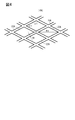
第2セル22Aは、例えば、平行四辺形形状をなし、典型的には、図4に例示するように、4辺の長さが等しい菱形形状をなす。図4に例示した第2セル22Aは、2つの鈍角と、2つの鋭角とを有する。対角関係にある鈍角の交差角度α1は90°超の同一角度であり、鋭角の交差角度β1は90°未満の同一角度である。
鋭角である交差角度β1は、70°以下であることが好ましい。この場合、モアレを低減するのに有効である。ただし、β1が過度に小さい場合にもモアレが発生し易くなる。これを回避するべく、β1は、30°~70°の範囲内、さらには45°~70°の範囲内とすることが好ましい。
第2セル22Aは、図4に例示した横長の菱形に限定されるものではなく、縦長の菱形であってもよいことは勿論である。これらの角度はディスプレイの画素とモアレを発生しないように設計されるのが好ましい。
第2セル22Aにおいて、細線20Aの幅方向寸法(線幅W1)は、好ましくは10μm以下であり、一層好ましくは5μm以下に設定される。これにより細線20Aによる導電パターンのモアレ及び細線見えが改善され、視認性が良好となる(すなわち、メッシュをなす細線20Aが視認され難くなる)。なお、導電シートとして必要な導電性を確保するべく、細線20Aの幅方向寸法は1μm以上であることが好ましい。
図2及び図4では菱形の例を記載しているが、第2セル22Aは第1セル22Bと同様にランダムセルであってもよく、また、六角形や三角形等、別の多角形から構成された定型パターンであってもよい。第2セル22Aは、ランダム又は菱形とするのが好ましく、菱形とするのがより好ましい。また、第2セル22Aから構成される第2メッシュ電極が上方電極となっても下方電極となってもよいが、菱形のセルを採用した場合には下方電極となるのがより好ましい。
図2に示すように、各下方電極18Aの一方の端部は、第1結線部40aを介して第1端子配線パターン42aに電気的に接続されている。
一方、第2シート体10Bを構成する第2透明基体14B(図3参照)の一主面上に形成された上方電極18Bは、図2に示すように、それぞれ第2方向(x方向)に延びる複数の帯状のパターンを有する。これら複数の上方電極18Bは、第1方向(y方向)に沿って配列されている。すなわち、積層導電シート12では、図3に示すように、絶縁性の第2透明基体14Bを介して下方電極18Aと上方電極18Bが対向する。
各上方電極18Bも下方電極18Aと同様に、細線20B同士が交差することにより形成される。この交差に伴って、細線20Bによって囲繞される空間(開口部)、すなわち、第1セル22Bが形成される。
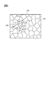
第1セル22Bの一例を図5に示す。この場合、ハッチングで示した第1セル22Bは、頂点C1及び頂点C2を直線で結ぶ細線20pと、頂点C2及び頂点C3を直線で結ぶ細線20qと、頂点C3及び頂点C4を直線で結ぶ細線20rと、頂点C4及び頂点C1を直線で結ぶ細線20sとで形成され、多角形形状をなしている。その他のセル(第1セル22B)も同様に、多角形形状を呈している。要するに、上方電極18Bは、第1セル22Bの形状が互いに異なり、規則性(統一性)が低いランダム形状のセルからなるメッシュである。
図5に示すランダムパターンにおいて、平均セルピッチ(以下、必要に応じて「Ps」と表すこともある)は50~400μmであることが好ましく、50μm~300μmであることが一層好ましい。ここで、平均セルピッチは、電極が延在する方向の第1セル22Bの最大の長さを任意の30個のセルで測定し、その平均長で定義される。
細線20Bの幅方向寸法(線幅)は、特に限定されるものではなく、例えば、10μm以下に設定することができるが、5μm以下が好ましい。第1セル22Bの形状がランダムであることと、細線20Bの線幅がこのように小さいこととが相俟って、モアレが改善されて視認性が良好となる。線幅は、4μm以下とすることが一層好ましい。なお、導電シートとして必要な導電性を確保するべく、細線20Bの線幅は1μm以上であることが好ましい。
ここで、上方電極18Bの平均セルピッチPsは、好ましくは50μmより大きく3200μm以下の範囲内で、且つ下方電極18Aの平均セルピッチPdに比して大きく設定される。なお、下方電極18Aの平均セルピッチPdは、上方電極18Bと同様に、電極が延在する方向の第2セル22Aの最大長を測定し、任意の30個の第2セル22Aの長さを平均した算出値として定義される。
そして、平均セルピッチPsは、平均セルピッチPdの1倍より大きく8倍以下である。要するに、平均セルピッチPsと平均セルピッチPdとの間には、以下の関係式が成り立つ。
1<Ps/Pd≦8
1<Ps/Pd≦8
すなわち、例えば、第2セル22Aの平均セルピッチPdが100μmであるときには、第1セル22Bの平均セルピッチPsは100μmより大きく800μm以下の範囲内に設定される。また、第2セル22Aの平均セルピッチPdが250μmであるときには、第1セル22Bの平均セルピッチPsは、250μmより大きく2000μm以下の範囲内に設定される。
このように、上方電極18Bの平均セルピッチPsを、下方電極18Aの平均セルピッチPdよりも所定の範囲内で大きくすることにより、Ps/Pdが1である場合、換言すれば、第2セル22Aの平均セルピッチPdと第1セル22Bの平均セルピッチPsが等しい場合に比して、指による押圧(タッチ)前後での静電容量の変化量が大きくなる。この点については後述する。
図2に示すように、各上方電極18Bの一方の端部は、第2結線部40bを介して第2端子配線パターン42bに電気的に接続されている。
ここで、下方電極18Aのx方向に向かう幅方向寸法(電極幅)をWd、上方電極18Bのy方向に向かう幅方向寸法(電極幅)をWsとするとき、Ws/Wdは、0.5以上1.5以下に設定することができる。すなわち、この場合、上方に位置する上方電極18Bの電極幅Wsを、下方に位置する下方電極18Aの電極幅Wdよりも小さくすることは必須ではなく、場合によっては、電極幅Wsと電極幅Wdを同一とすることや、電極幅Wsを電極幅Wdよりも大きくすることが可能である。勿論、電極幅Wsを電極幅Wdよりも小さくするようにしてもよい。
Ws/Wdは、0.8以上1.2以下である構成がより好ましい。下方電極18Aと上方電極18Bの幅を同程度とすることで、タッチ領域に対する縦方向の感度と横方向の感度が等しくなるためより好ましい。
以上のように構成される上方電極18Bの有効電極面積は、タッチ有効面積の70%以上であることが好ましい。これにより、上方電極18Bの導電性を高くし易くなる。ここで、有効電極面積とは、上方電極18Bが表示領域内で覆う面積の割合を示す。具体的には、図2において、上方電極18Bの電極幅Wsとセンサ部112のy方向の長さと上方電極18Bの電極数との積を、センサ部112の面積で除して算出した値である。なお、互いに隣接する上方電極18B同士の間にダミー電極が存在する場合には、当該ダミー電極は有効電極面積に含めない。
タッチパネル100に適用した第1シート体10Aは、図2に示すように、センサ部112に対応した部分に、上述した多数の下方電極18Aが配列され、端子配線部114には各第1結線部40aから導出された第1端子配線パターン42aが配列されている。
図1の例では、端子配線部114のうち、第1シート体10Aの一方の長辺側(x方向)の周縁部には、その長さ方向中央部分に、複数の第1端子116aが前記一方の長辺の長さ方向に配列形成されている。また、センサ部112の短辺(y方向)に沿って、下方電極18Aと接続される複数の第1結線部40aが直線状に配列されている。各第1結線部40aから導出された第1端子配線パターン42aは、第1シート体10Aの端子配線部114を引き回され、それぞれ対応する第1端子116aに電気的に接続されている。
一方、第2シート体10Bの外形は、上面から見て長方形状を有し、センサ部112の外形も長方形状を有する。端子配線部114のうち、第2シート体10Bの一方の長辺側(x方向)の周縁部には、その長さ方向中央部分に、複数の第2端子116bが前記一方の長辺の長さ方向に配列形成されている。また、センサ部112の一方の長辺に沿って、上方電極18Bと接続される複数の第2結線部40bが直線状に配列されている。各第2結線部40bから導出された第2端子配線パターン42bは、第2シート体10Bの一方の長辺における略中央部に向かって引き回され、それぞれ対応する第2端子116bに電気的に接続されている。
なお、第1端子配線パターン42aの導出形態を上述した第2端子配線パターン42bと同様にしてもよいし、逆に、第2端子配線パターン42bの導出形態を上述した第1端子配線パターン42aと同様にしてもよい。
積層導電シート12は、図3に示すように、第1シート体10Aに第2シート体10Bが積層されて構成される。この際、第1シート体10Aの上端面(すなわち、下方電極18A及び第1透明基体14A上)と、第2シート体10Bの下端面との間に、粘着シートとして貼付された粘着剤(OCAとも指称される)30が配置してもよい。
このようにして形成された積層導電シート12において、下方電極18Aと上方電極18Bが重なった箇所(重なり部分)の一例を、平面図として図6に示す。図6中の太実線が下方電極18A(定型メッシュパターン)の第2セル22A(小ピッチ)であり、細実線が上方電極18B(ランダムメッシュパターン)の第1セル22B(大ピッチ)である。
以上のように構成される下方電極18A、上方電極18Bを含んだ積層導電シート12をタッチパネル100として使用する場合は、第2シート体10B上に保護層106を形成してもよい。なお、第2シート体10Bの上端面と保護層106の下端面との間にも、粘着シートとしての粘着剤(OCA)30が配置されるのが好ましい。そして、第1シート体10Aの多数の下方電極18Aから導出された第1端子配線パターン42aと、第2シート体10Bの多数の上方電極18Bから導出された第2端子配線パターン42bとを、例えば、スキャンをコントロールする制御回路に接続する。
下方電極18A及び上方電極18Bは、線幅の狭いパターンを得るために、好適には、フォトリソプロセスを使用したエッチング、あるいはマイクロコンタクト印刷パターニング法又は銀塩法によって形成することができる。大量のパターンを繰り返し得るためには、銀塩法がより好ましい。
マイクロコンタクト印刷パターニング法とは、マイクロコンタクト印刷法を利用して線幅が狭いパターンを得る方法である。ここで、マイクロコンタクト印刷法は、弾力性のあるポリジメチルシロキサンのスタンプを用い、チオール溶液をインキとして金基材に接触させて単分子膜のパターンを作製する方法である(Whitesedes著、Angew.Chem.Int.Ed.,1998年第37巻第550頁参照)。
マイクロコンタクト印刷パターニング法の代表的なプロセスは、例えば、以下の通りである。すなわち、先ず、基材に金属がコーティングされる(例えば、銀が、PET基材にスパッタコーティングされる)。
次に、単分子膜のマスキングが、金属がコーティングされた基材にマイクロコンタクト印刷法を用いてスタンピングされる。その後、マスキング下のパターンを除いて、基材にコーティングされた金属がエッチングにより除去される。
以上につき、その具体的な作業等は、特表2012-519329号公報の段落<0104>に詳述されている。
一方、銀塩法は、感光性銀塩含有層を有する感光材料を露光・現像することにより、メッシュ状をなす細線20A、20Bのパターンを得るものである。その具体的な作業等は、特開2009-4348号公報の段落<0163>~<0241>に詳述されている。
本発明は、上記した実施の形態に特に限定されるものではなく、本発明の主旨を逸脱しない範囲で種々の変更が可能である。
例えば、上記したように、下方電極18A及び上方電極18Bの双方をランダムメッシュパターンとしてもよい。なお、下方電極18A又は上方電極18Bのいずれか一方がランダムメッシュパターン、残余の一方が定型メッシュパターンであることが好ましい。
下方電極18Aをランダムメッシュパターン、上方電極18Bを定型メッシュパターンとするようにしてもよいが、下方電極18Aを定型メッシュパターン、上方電極18Bをランダムメッシュパターンとした態様が最も好ましい。この理由は、ランダムメッシュは、細線をランダム配置するために、定型パターンに比較して導電性に寄与が小さい無駄な線分が発生してしまう。このため、ランダムメッシュでは、導電性が同等である定型メッシュと比較すると、透過率が僅かに低下する傾向がある。よって、平均セルピッチが小さい下方電極には無駄の少ない定型メッシュパターンを採用し、平均セルピッチが大きい上方電極にランダムメッシュパターンを採用するのが最も好ましい。
いずれの場合においても、上方電極18Bの平均セルピッチPsを、下方電極18Aの平均セルピッチPdよりも大きく、1より大きく8以下(好ましくは2~6)の範囲内とする。
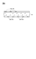
また、上記した実施の形態では、電極幅Ws、Wdを一定としているが(図2参照)、図7に示すように、例えば、下方電極18Aの一部の電極幅を、長手方向に延在する途中で狭くするようにしてもよい。この場合、電極幅が狭い部位が上方電極18Bの上方に配置されるようにすればよい。
図7とは逆に、下方電極18Aの一部の電極幅を小さくするようにしてもよい。この場合、電極幅が小さい部位の上方に上方電極18Bを配置すればよい。また、下方電極18A及び上方電極18Bの双方につき、一部の電極幅を、長手方向に延在する途中で小さくし、電極幅が小さくなった部位同士を積層配置するようにしてもよい。
この場合、下方電極18Aと上方電極18Bが対向する箇所での静電容量の初期値が小さくなる。従って、S/N比の向上を図ることができる。
さらに、第2セル22A(下方電極18A)において、本来であれば第1セル22B(上方電極18B)と対向すべき箇所の細線の一部を、線幅を小さくしたり、断線部としたりすることも好ましい。換言すれば、下方電極18Aをなす細線20Aに、上方電極18Bとの対向する箇所に幅狭部や断線部を設けるようにするとよい。勿論、これとは逆に、上方電極18Bをなす細線20Bの、下方電極18Aとの交差箇所の一部を切断するようにしてもよい。
この場合、断線部では寄生容量が小さくなる。すなわち、静電容量の初期値が小さくなる。静電容量の初期値が大きい場合、操作者による指での押圧に伴って静電容量が変化したときに、S/N比を向上させることが容易でなくなるが、下方電極18Aと上方電極18Bが対向する箇所で対向する面積を減少させる設計をすることにより、S/N比の向上を図ることができる。
そして、積層導電シート12は、第1透明基体14Aの一主面に下方電極18Aを形成し、第2透明基体14Bの一主面に上方電極18Bを形成して積層するもの(図2及び図3参照)に限定されるものではない。すなわち、図8に示すように、第1透明基体14Aの一主面に下方電極18Aが形成され、且つ該第1透明基体14Aの他主面に上方電極18Bが形成されたものであってもよい。この場合、第2透明基体14Bが存在せず、下方電極18A上に第1透明基体14Aが積層され、第1透明基体14A上に上方電極18Bが積層された形態となる。
いずれの場合においても、積層導電シート12の用途は、タッチパネル100のセンサ本体102に特に限定されるものではなく、無機EL素子、有機EL素子、あるいは太陽電池等の各種電極に用いることも可能である。さらに、電極以外にも、電流を流すことで発熱する透明発熱体(例えば、車両のデフロスタ)、電磁波を遮断する電磁波シールド材にも適用可能である。
電極幅Wdが5mm、平均セルピッチPdが300μmである下方電極18Aを透明基体上に1本形成した導電シートと、電極幅Wsが5mmである上方電極18Bを透明基体上に1本形成した導電シートとを、OCAを介して貼り合わせて電極積層体を得た。勿論、下方電極と上方電極の一部同士を対向させた。
この構成において、上方電極の平均セルピッチPsを下記の表1に示すように種々変更し、実施例1~7、比較例1、2の電極積層体を構成した。その後、各電極積層体におけるタッチ前後の静電容量の変化量(ΔCm値)を求めた。ΔCmの値が大きいほど、タッチしたことを検出できる可能性が高まり、検出精度が良好となる。

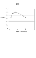
結果を、横軸をPs/Pd(平均セルピッチ倍率)、縦軸をΔCmとするグラフにして図9に示す。この図9から、Ps/Pdが1よりも大きく且つ8以下の範囲内であると、Ps/Pd=1(比較例1)のときよりもΔCmが向上することが分かる。特に、Ps/Pdが2~6である場合、換言すれば、第1セル22B(上方電極18B)の平均セルピッチPsが、第2セル22A(下方電極18A)の平均セルピッチPdの2倍~6倍であるときに顕著である。このことは、S/N比、ひいてはタッチ検出精度を向上させ得ることを意味する。
この理由は、平均セルピッチPsを平均セルピッチPdに比して大きくしたことに伴って、下方電極18Aのメッシュから上方電極18Bのメッシュに向かう電界が、上方電極18Bのセルの開口を容易に通るようになり、このために指による押圧の前後における静電容量の変化量が大きくなるからである。従って、上方電極18Bの電極幅Wsを小さくすることなく、タッチ検出の精度を向上させることができる。
なお、Ps/Pdが3となる付近をピークとして低下していく理由としては、上方電極の平均セルピッチPsが大きくなるにつれ、上方電極の開口の中心付近に位置する下方電極の、上方電極からの距離が遠くなるので、該下方電極からの電界が上方電極に及ぼす影響が低下するためにΔCm値への寄与が少なくなることが考えられる。よって、上方電極の平均セルピッチPsが大きければ大きいほど好ましいということにはならず、好ましい範囲を持つ。
表1には、実施例1~7、比較例1、2の電極積層体のモアレ評価を併せて示している。ここで、表1中の「A」は、評価者が注意深く確認してもモアレが認められなかったことを示す。表1から、Ps/Pdが1よりも大きく8以下であるときには、Ps/Pd=1.5、Ps/Pd=2.5であるとき(実施例1、3)のモアレ評価を参照して明らかな通り、Ps/Pdが自然数とならない場合にもモアレが発生しないことが分かる。
これは、一方の電極がランダムセルから構成されるため、上方電極と下方電極のピッチの違いに起因するモアレ(周期的な干渉)の発生が抑制されるからである。上方電極と下方電極の双方を菱形等からなる定型パターンとした場合には、ピッチの違いに起因して周期的に干渉の粗密が発生し、強いモアレが視認されることとなるために採用可能なPs/Pdは厳密に限定される。これに対し、ランダムセルを有するメッシュを採用した場合、Ps/Pdは1よりも大きく8以下の範囲であれば如何なる値であっても設定できる。このため、設計自由度が高くなる。
以上のことから、Ps/Pdを1よりも大きく8以下、一層好ましくは2~6の範囲内とすることにより、タッチパネル100(表示装置108)において、モアレが低減し且つタッチ検出精度を高くすることができる。
しかも、上方電極18Bの電極幅Wsを極端に小さくする必要がないので、第1セル22Bの平均セルピッチを小さくする必要もない。このために該上方電極18Bの透過率が低下することを回避し得るので、透過率が良好となる。
10A…第1シート体 10B…第2シート体
12…積層導電シート(導電シート) 14A…第1透明基体
14B…第2透明基体 18A…下方電極
18B…上方電極 20A、20B…細線
22A…第2セル 22B…第1セル
30…粘着剤(OCA) 100…タッチパネル
102…センサ本体 106…保護層
108…表示装置 110…表示パネル
112…センサ部 114…端子配線部
12…積層導電シート(導電シート) 14A…第1透明基体
14B…第2透明基体 18A…下方電極
18B…上方電極 20A、20B…細線
22A…第2セル 22B…第1セル
30…粘着剤(OCA) 100…タッチパネル
102…センサ本体 106…保護層
108…表示装置 110…表示パネル
112…センサ部 114…端子配線部
Claims (11)
- 下方電極と上方電極とが、絶縁層を介して積層された導電シートにおいて、
前記下方電極又は前記上方電極の少なくともいずれか一方が、金属線材同士が交差することにより形成される複数個の第1セルが連なった第1メッシュ電極からなり、前記複数個の第1セルの形状が互いに異なるランダムセルであって、且つ前記第1メッシュ電極は、第1の方向に沿って延在するとともに、前記第1の方向に対して直交する第2の方向に沿って複数個並列され、
前記上方電極又は前記下方電極の残余の一方が、金属線材同士が交差することにより形成される複数個の第2セルが連なった第2メッシュ電極からなり、且つ前記第2メッシュ電極は、前記第2の方向に沿って延在するとともに、前記第1の方向に沿って複数個並列され、
前記下方電極の平均セルピッチをPd、前記上方電極の平均セルピッチをPsとするとき、Ps/Pdが1より大きく8以下であることを特徴とする導電シート。 - 請求項1記載の導電シートにおいて、Ps/Pdが2以上6以下である導電シート。
- 請求項1又は2記載の導電シートにおいて、前記上方電極の有効電極面積がタッチ有効面積の70%以上である導電シート。
- 請求項1~3のいずれか1項に記載の導電シートにおいて、前記下方電極の電極幅をWd、前記上方電極の電極幅をWsとするとき、Ws/Wdが0.5以上1.5以下である導電シート。
- 請求項1~4のいずれか1項に記載の導電シートにおいて、前記第2セルが菱形である導電シート。
- 請求項1~5のいずれか1項に記載の導電シートにおいて、前記下方電極の平均セルピッチPdが50μm以上400μm以下であり、且つ前記上方電極の平均セルピッチPsが50μmより大きく3200μm以下である導電シート。
- 請求項1~6のいずれか1項に記載の導電シートにおいて、前記第1メッシュ電極が前記上方電極である導電シート。
- 請求項1~7のいずれか1項に記載の導電シートにおいて、前記下方電極と前記上方電極の対向箇所にて、前記下方電極又は前記上方電極の少なくともいずれか一方の電極幅が対向箇所以外の部位に比して小さく設定されている導電シート。
- 請求項1~8のいずれか1項に記載の導電シートにおいて、前記下方電極と前記上方電極の対向箇所の一部に、第1セルを形成する金属線材又は第2セルを形成する金属線材の少なくともいずれか一方が切断された断線部が設けられている導電シート。
- 請求項1~9のいずれか1項に記載された導電シートを有することを特徴とする静電容量式タッチパネル。
- 請求項10に記載された静電容量式タッチパネルを有することを特徴とする表示装置。
Priority Applications (3)
| Application Number | Priority Date | Filing Date | Title |
|---|---|---|---|
| KR1020167013872A KR101850636B1 (ko) | 2013-12-03 | 2014-10-01 | 도전 시트, 정전 용량식 터치 패널 및 표시 장치 |
| CN201480062942.0A CN105745609A (zh) | 2013-12-03 | 2014-10-01 | 导电片、静电电容式触摸面板和显示装置 |
| US15/167,366 US10073573B2 (en) | 2013-12-03 | 2016-05-27 | Conductive sheet, capacitive touch panel, display device |
Applications Claiming Priority (2)
| Application Number | Priority Date | Filing Date | Title |
|---|---|---|---|
| JP2013-250335 | 2013-12-03 | ||
| JP2013250335A JP6010012B2 (ja) | 2013-12-03 | 2013-12-03 | 導電シート、静電容量式タッチパネル及び表示装置 |
Related Child Applications (1)
| Application Number | Title | Priority Date | Filing Date |
|---|---|---|---|
| US15/167,366 Continuation US10073573B2 (en) | 2013-12-03 | 2016-05-27 | Conductive sheet, capacitive touch panel, display device |
Publications (1)
| Publication Number | Publication Date |
|---|---|
| WO2015083424A1 true WO2015083424A1 (ja) | 2015-06-11 |
Family
ID=53273201
Family Applications (1)
| Application Number | Title | Priority Date | Filing Date |
|---|---|---|---|
| PCT/JP2014/076305 Ceased WO2015083424A1 (ja) | 2013-12-03 | 2014-10-01 | 導電シート、静電容量式タッチパネル及び表示装置 |
Country Status (6)
| Country | Link |
|---|---|
| US (1) | US10073573B2 (ja) |
| JP (1) | JP6010012B2 (ja) |
| KR (1) | KR101850636B1 (ja) |
| CN (1) | CN105745609A (ja) |
| TW (1) | TWI628565B (ja) |
| WO (1) | WO2015083424A1 (ja) |
Cited By (2)
| Publication number | Priority date | Publication date | Assignee | Title |
|---|---|---|---|---|
| CN106843558A (zh) * | 2015-12-04 | 2017-06-13 | 介面光电股份有限公司 | 触控面板的感测金属网格及其制法 |
| EP3276471A1 (en) * | 2016-07-29 | 2018-01-31 | NCR Corporation | Touchscreen defroster |
Families Citing this family (15)
| Publication number | Priority date | Publication date | Assignee | Title |
|---|---|---|---|---|
| CN104216598A (zh) * | 2014-08-29 | 2014-12-17 | 合肥鑫晟光电科技有限公司 | 触摸基板及其制作方法、触摸显示装置 |
| US9958973B2 (en) * | 2014-10-24 | 2018-05-01 | Lg Display Co., Ltd. | Touch panel and touch panel-integrated organic light emitting display device |
| KR20160086495A (ko) * | 2015-01-09 | 2016-07-20 | 삼성디스플레이 주식회사 | 터치 스크린 패널 및 이를 구비하는 표시 장치 |
| JP6879678B2 (ja) * | 2015-06-22 | 2021-06-02 | 株式会社半導体エネルギー研究所 | 半導体装置 |
| WO2017018051A1 (ja) * | 2015-07-24 | 2017-02-02 | 富士フイルム株式会社 | タッチパネル用導電フィルムのメッシュパターン設計方法、タッチパネル用導電フィルムの製造方法およびタッチパネル用導電フィルム |
| JP2017058827A (ja) * | 2015-09-15 | 2017-03-23 | 株式会社村田製作所 | タッチパネル及び電子機器 |
| TW201721377A (zh) * | 2015-12-04 | 2017-06-16 | 介面光電股份有限公司 | 觸控面板之感測金屬網格及其製法 |
| CN108062187A (zh) * | 2016-11-07 | 2018-05-22 | 京东方科技集团股份有限公司 | 触控结构及其制作方法和触控装置 |
| CN107037925B (zh) * | 2017-03-30 | 2019-12-24 | 昆山国显光电有限公司 | 触控屏及其制备方法及触控显示装置 |
| JP6878155B2 (ja) * | 2017-06-05 | 2021-05-26 | 株式会社Vtsタッチセンサー | 導電性フィルム、タッチパネル、および、表示装置 |
| TWI657359B (zh) * | 2017-11-24 | 2019-04-21 | 友達光電股份有限公司 | 觸控裝置 |
| JP7469485B2 (ja) * | 2020-08-27 | 2024-04-16 | 富士フイルム株式会社 | タッチパネル用導電部材およびタッチパネル |
| KR102766427B1 (ko) * | 2020-08-28 | 2025-02-12 | 동우 화인켐 주식회사 | 도전성 메쉬 구조체의 및 이를 포함하는 안테나 소자 |
| CN113093954B (zh) * | 2021-05-18 | 2025-01-17 | 深圳市志凌伟业光电有限公司 | 触摸屏及显示装置 |
| WO2023233824A1 (ja) * | 2022-05-31 | 2023-12-07 | パナソニックIpマネジメント株式会社 | タッチセンサ |
Citations (4)
| Publication number | Priority date | Publication date | Assignee | Title |
|---|---|---|---|---|
| JP2012033147A (ja) * | 2010-07-05 | 2012-02-16 | Fujifilm Corp | タッチパネル及び導電シート |
| JP2012243058A (ja) * | 2011-05-19 | 2012-12-10 | Panasonic Corp | タッチパネル装置およびこれを備えたプラズマディスプレイ装置 |
| JP2013054619A (ja) * | 2011-09-06 | 2013-03-21 | Fujifilm Corp | 導電シート、タッチパネル及び表示装置 |
| JP5224203B1 (ja) * | 2012-07-11 | 2013-07-03 | 大日本印刷株式会社 | タッチパネルセンサ、タッチパネル装置および表示装置 |
Family Cites Families (15)
| Publication number | Priority date | Publication date | Assignee | Title |
|---|---|---|---|---|
| EP2401669B1 (en) | 2009-02-26 | 2016-04-06 | 3M Innovative Properties Company | Touch screen sensor and patterned substrate having overlaid micropatterns with low visibility |
| JP2011059772A (ja) | 2009-09-07 | 2011-03-24 | Hitachi Chem Co Ltd | 網目状導電性パターン、導体層パターン付き基材及びタッチパネル部材 |
| CN103649883B (zh) * | 2011-07-11 | 2017-09-08 | 富士胶片株式会社 | 导电片及其制造方法、触摸屏以及显示装置 |
| US9330544B2 (en) * | 2012-11-20 | 2016-05-03 | Immersion Corporation | System and method for simulated physical interactions with haptic effects |
| KR101598249B1 (ko) * | 2013-01-29 | 2016-02-26 | 삼성전기주식회사 | 터치패널 |
| CN103176680B (zh) * | 2013-03-08 | 2015-05-13 | 南昌欧菲光科技有限公司 | 触控面板及其制造方法 |
| WO2015045060A1 (ja) * | 2013-09-26 | 2015-04-02 | 富士通株式会社 | 電子機器、及び、電子機器における照合方法 |
| WO2015045064A1 (ja) * | 2013-09-26 | 2015-04-02 | 富士通株式会社 | 駆動制御装置、電子機器、及び駆動制御方法 |
| MX338463B (es) * | 2013-09-26 | 2016-04-15 | Fujitsu Ltd | Aparato de control de accionador, dispositivo electronico y metodo de control del accionador. |
| JP6183476B2 (ja) * | 2014-02-14 | 2017-08-23 | 富士通株式会社 | 電子機器及び駆動制御方法 |
| JPWO2015121972A1 (ja) * | 2014-02-14 | 2017-03-30 | 富士通株式会社 | 駆動制御装置、電子機器、システム、及び駆動制御方法 |
| JPWO2015121955A1 (ja) * | 2014-02-14 | 2017-03-30 | 富士通株式会社 | 電子機器、入力装置、及び駆動制御方法 |
| GB2530036A (en) * | 2014-09-09 | 2016-03-16 | Ultrahaptics Ltd | Method and apparatus for modulating haptic feedback |
| JP6406025B2 (ja) * | 2015-01-16 | 2018-10-17 | 富士通株式会社 | 電子機器 |
| SG11201706557SA (en) * | 2015-02-20 | 2017-09-28 | Ultrahaptics Ip Ltd | Perceptions in a haptic system |
-
2013
- 2013-12-03 JP JP2013250335A patent/JP6010012B2/ja not_active Expired - Fee Related
-
2014
- 2014-10-01 WO PCT/JP2014/076305 patent/WO2015083424A1/ja not_active Ceased
- 2014-10-01 CN CN201480062942.0A patent/CN105745609A/zh active Pending
- 2014-10-01 KR KR1020167013872A patent/KR101850636B1/ko not_active Expired - Fee Related
- 2014-11-13 TW TW103139417A patent/TWI628565B/zh not_active IP Right Cessation
-
2016
- 2016-05-27 US US15/167,366 patent/US10073573B2/en active Active
Patent Citations (4)
| Publication number | Priority date | Publication date | Assignee | Title |
|---|---|---|---|---|
| JP2012033147A (ja) * | 2010-07-05 | 2012-02-16 | Fujifilm Corp | タッチパネル及び導電シート |
| JP2012243058A (ja) * | 2011-05-19 | 2012-12-10 | Panasonic Corp | タッチパネル装置およびこれを備えたプラズマディスプレイ装置 |
| JP2013054619A (ja) * | 2011-09-06 | 2013-03-21 | Fujifilm Corp | 導電シート、タッチパネル及び表示装置 |
| JP5224203B1 (ja) * | 2012-07-11 | 2013-07-03 | 大日本印刷株式会社 | タッチパネルセンサ、タッチパネル装置および表示装置 |
Cited By (3)
| Publication number | Priority date | Publication date | Assignee | Title |
|---|---|---|---|---|
| CN106843558A (zh) * | 2015-12-04 | 2017-06-13 | 介面光电股份有限公司 | 触控面板的感测金属网格及其制法 |
| EP3276471A1 (en) * | 2016-07-29 | 2018-01-31 | NCR Corporation | Touchscreen defroster |
| US10067599B2 (en) | 2016-07-29 | 2018-09-04 | Ncr Corporation | Touchscreen defroster |
Also Published As
| Publication number | Publication date |
|---|---|
| TW201523388A (zh) | 2015-06-16 |
| KR101850636B1 (ko) | 2018-04-19 |
| JP6010012B2 (ja) | 2016-10-19 |
| US20160274702A1 (en) | 2016-09-22 |
| TWI628565B (zh) | 2018-07-01 |
| CN105745609A (zh) | 2016-07-06 |
| JP2015108885A (ja) | 2015-06-11 |
| US10073573B2 (en) | 2018-09-11 |
| KR20160075722A (ko) | 2016-06-29 |
Similar Documents
| Publication | Publication Date | Title |
|---|---|---|
| JP6010012B2 (ja) | 導電シート、静電容量式タッチパネル及び表示装置 | |
| JP6068322B2 (ja) | 導電シート、静電容量式タッチパネル及び表示装置 | |
| KR101867749B1 (ko) | 터치 패널용 도전 시트 및 정전 용량식 터치 패널 | |
| JP6170420B2 (ja) | 導電シート及びタッチパネル | |
| JP5174745B2 (ja) | タッチスイッチ | |
| US10048820B2 (en) | Touch panel and manufacturing method thereof | |
| JP6384058B2 (ja) | タッチスクリーン、タッチパネル、タッチパネル付き表示装置および電子機器 | |
| US20100328248A1 (en) | Capacitive touch screen with reduced electrode trace resistance | |
| CN110502152B (zh) | 触控面板、触控显示面板及触控显示装置 | |
| KR101357585B1 (ko) | 터치패널의 전극 패턴 및 그 제조 방법 | |
| CN107111392A (zh) | 导电性薄膜及具备该导电性薄膜的触摸面板传感器 | |
| KR20130072402A (ko) | 터치패널의 전극형성방법 | |
| KR101105692B1 (ko) | 터치 패널용 면상 부재 제조 방법 | |
| JP6109767B2 (ja) | タッチパネル用電極積層体、静電容量式タッチパネル及び三次元タッチパネル付表示装置 | |
| JPWO2018225633A1 (ja) | タッチパネルセンサー用部材 | |
| CN212624008U (zh) | 导电薄膜、触控模组及电子设备 | |
| TW201944216A (zh) | 透明導電薄膜降低局部區域阻抗值的方法及其製成品 | |
| KR20140014593A (ko) | 연결부의 구조가 개선된 터치패널 |
Legal Events
| Date | Code | Title | Description |
|---|---|---|---|
| 121 | Ep: the epo has been informed by wipo that ep was designated in this application |
Ref document number: 14867189 Country of ref document: EP Kind code of ref document: A1 |
|
| ENP | Entry into the national phase |
Ref document number: 20167013872 Country of ref document: KR Kind code of ref document: A |
|
| NENP | Non-entry into the national phase |
Ref country code: DE |
|
| 122 | Ep: pct application non-entry in european phase |
Ref document number: 14867189 Country of ref document: EP Kind code of ref document: A1 |