WO2015079708A1 - エポキシ樹脂組成物、半導体封止剤および半導体装置 - Google Patents
エポキシ樹脂組成物、半導体封止剤および半導体装置 Download PDFInfo
- Publication number
- WO2015079708A1 WO2015079708A1 PCT/JP2014/005967 JP2014005967W WO2015079708A1 WO 2015079708 A1 WO2015079708 A1 WO 2015079708A1 JP 2014005967 W JP2014005967 W JP 2014005967W WO 2015079708 A1 WO2015079708 A1 WO 2015079708A1
- Authority
- WO
- WIPO (PCT)
- Prior art keywords
- component
- epoxy resin
- resin composition
- mass
- semiconductor
- Prior art date
- Legal status (The legal status is an assumption and is not a legal conclusion. Google has not performed a legal analysis and makes no representation as to the accuracy of the status listed.)
- Ceased
Links
Images


Classifications
-
- C—CHEMISTRY; METALLURGY
- C08—ORGANIC MACROMOLECULAR COMPOUNDS; THEIR PREPARATION OR CHEMICAL WORKING-UP; COMPOSITIONS BASED THEREON
- C08L—COMPOSITIONS OF MACROMOLECULAR COMPOUNDS
- C08L63/00—Compositions of epoxy resins; Compositions of derivatives of epoxy resins
-
- C—CHEMISTRY; METALLURGY
- C08—ORGANIC MACROMOLECULAR COMPOUNDS; THEIR PREPARATION OR CHEMICAL WORKING-UP; COMPOSITIONS BASED THEREON
- C08G—MACROMOLECULAR COMPOUNDS OBTAINED OTHERWISE THAN BY REACTIONS ONLY INVOLVING UNSATURATED CARBON-TO-CARBON BONDS
- C08G59/00—Polycondensates containing more than one epoxy group per molecule; Macromolecules obtained by polymerising compounds containing more than one epoxy group per molecule using curing agents or catalysts which react with the epoxy groups
- C08G59/18—Macromolecules obtained by polymerising compounds containing more than one epoxy group per molecule using curing agents or catalysts which react with the epoxy groups ; e.g. general methods of curing
- C08G59/20—Macromolecules obtained by polymerising compounds containing more than one epoxy group per molecule using curing agents or catalysts which react with the epoxy groups ; e.g. general methods of curing characterised by the epoxy compounds used
- C08G59/22—Di-epoxy compounds
- C08G59/24—Di-epoxy compounds carbocyclic
-
- C—CHEMISTRY; METALLURGY
- C08—ORGANIC MACROMOLECULAR COMPOUNDS; THEIR PREPARATION OR CHEMICAL WORKING-UP; COMPOSITIONS BASED THEREON
- C08G—MACROMOLECULAR COMPOUNDS OBTAINED OTHERWISE THAN BY REACTIONS ONLY INVOLVING UNSATURATED CARBON-TO-CARBON BONDS
- C08G59/00—Polycondensates containing more than one epoxy group per molecule; Macromolecules obtained by polymerising compounds containing more than one epoxy group per molecule using curing agents or catalysts which react with the epoxy groups
- C08G59/18—Macromolecules obtained by polymerising compounds containing more than one epoxy group per molecule using curing agents or catalysts which react with the epoxy groups ; e.g. general methods of curing
- C08G59/20—Macromolecules obtained by polymerising compounds containing more than one epoxy group per molecule using curing agents or catalysts which react with the epoxy groups ; e.g. general methods of curing characterised by the epoxy compounds used
- C08G59/22—Di-epoxy compounds
- C08G59/24—Di-epoxy compounds carbocyclic
- C08G59/245—Di-epoxy compounds carbocyclic aromatic
-
- C—CHEMISTRY; METALLURGY
- C08—ORGANIC MACROMOLECULAR COMPOUNDS; THEIR PREPARATION OR CHEMICAL WORKING-UP; COMPOSITIONS BASED THEREON
- C08G—MACROMOLECULAR COMPOUNDS OBTAINED OTHERWISE THAN BY REACTIONS ONLY INVOLVING UNSATURATED CARBON-TO-CARBON BONDS
- C08G59/00—Polycondensates containing more than one epoxy group per molecule; Macromolecules obtained by polymerising compounds containing more than one epoxy group per molecule using curing agents or catalysts which react with the epoxy groups
- C08G59/18—Macromolecules obtained by polymerising compounds containing more than one epoxy group per molecule using curing agents or catalysts which react with the epoxy groups ; e.g. general methods of curing
- C08G59/40—Macromolecules obtained by polymerising compounds containing more than one epoxy group per molecule using curing agents or catalysts which react with the epoxy groups ; e.g. general methods of curing characterised by the curing agents used
-
- C—CHEMISTRY; METALLURGY
- C08—ORGANIC MACROMOLECULAR COMPOUNDS; THEIR PREPARATION OR CHEMICAL WORKING-UP; COMPOSITIONS BASED THEREON
- C08G—MACROMOLECULAR COMPOUNDS OBTAINED OTHERWISE THAN BY REACTIONS ONLY INVOLVING UNSATURATED CARBON-TO-CARBON BONDS
- C08G59/00—Polycondensates containing more than one epoxy group per molecule; Macromolecules obtained by polymerising compounds containing more than one epoxy group per molecule using curing agents or catalysts which react with the epoxy groups
- C08G59/18—Macromolecules obtained by polymerising compounds containing more than one epoxy group per molecule using curing agents or catalysts which react with the epoxy groups ; e.g. general methods of curing
- C08G59/40—Macromolecules obtained by polymerising compounds containing more than one epoxy group per molecule using curing agents or catalysts which react with the epoxy groups ; e.g. general methods of curing characterised by the curing agents used
- C08G59/42—Polycarboxylic acids; Anhydrides, halides or low molecular weight esters thereof
-
- C—CHEMISTRY; METALLURGY
- C08—ORGANIC MACROMOLECULAR COMPOUNDS; THEIR PREPARATION OR CHEMICAL WORKING-UP; COMPOSITIONS BASED THEREON
- C08G—MACROMOLECULAR COMPOUNDS OBTAINED OTHERWISE THAN BY REACTIONS ONLY INVOLVING UNSATURATED CARBON-TO-CARBON BONDS
- C08G59/00—Polycondensates containing more than one epoxy group per molecule; Macromolecules obtained by polymerising compounds containing more than one epoxy group per molecule using curing agents or catalysts which react with the epoxy groups
- C08G59/18—Macromolecules obtained by polymerising compounds containing more than one epoxy group per molecule using curing agents or catalysts which react with the epoxy groups ; e.g. general methods of curing
- C08G59/40—Macromolecules obtained by polymerising compounds containing more than one epoxy group per molecule using curing agents or catalysts which react with the epoxy groups ; e.g. general methods of curing characterised by the curing agents used
- C08G59/50—Amines
-
- C—CHEMISTRY; METALLURGY
- C08—ORGANIC MACROMOLECULAR COMPOUNDS; THEIR PREPARATION OR CHEMICAL WORKING-UP; COMPOSITIONS BASED THEREON
- C08G—MACROMOLECULAR COMPOUNDS OBTAINED OTHERWISE THAN BY REACTIONS ONLY INVOLVING UNSATURATED CARBON-TO-CARBON BONDS
- C08G59/00—Polycondensates containing more than one epoxy group per molecule; Macromolecules obtained by polymerising compounds containing more than one epoxy group per molecule using curing agents or catalysts which react with the epoxy groups
- C08G59/18—Macromolecules obtained by polymerising compounds containing more than one epoxy group per molecule using curing agents or catalysts which react with the epoxy groups ; e.g. general methods of curing
- C08G59/40—Macromolecules obtained by polymerising compounds containing more than one epoxy group per molecule using curing agents or catalysts which react with the epoxy groups ; e.g. general methods of curing characterised by the curing agents used
- C08G59/50—Amines
- C08G59/5033—Amines aromatic
-
- C—CHEMISTRY; METALLURGY
- C08—ORGANIC MACROMOLECULAR COMPOUNDS; THEIR PREPARATION OR CHEMICAL WORKING-UP; COMPOSITIONS BASED THEREON
- C08G—MACROMOLECULAR COMPOUNDS OBTAINED OTHERWISE THAN BY REACTIONS ONLY INVOLVING UNSATURATED CARBON-TO-CARBON BONDS
- C08G59/00—Polycondensates containing more than one epoxy group per molecule; Macromolecules obtained by polymerising compounds containing more than one epoxy group per molecule using curing agents or catalysts which react with the epoxy groups
- C08G59/18—Macromolecules obtained by polymerising compounds containing more than one epoxy group per molecule using curing agents or catalysts which react with the epoxy groups ; e.g. general methods of curing
- C08G59/40—Macromolecules obtained by polymerising compounds containing more than one epoxy group per molecule using curing agents or catalysts which react with the epoxy groups ; e.g. general methods of curing characterised by the curing agents used
- C08G59/62—Alcohols or phenols
- C08G59/621—Phenols
-
- C—CHEMISTRY; METALLURGY
- C08—ORGANIC MACROMOLECULAR COMPOUNDS; THEIR PREPARATION OR CHEMICAL WORKING-UP; COMPOSITIONS BASED THEREON
- C08J—WORKING-UP; GENERAL PROCESSES OF COMPOUNDING; AFTER-TREATMENT NOT COVERED BY SUBCLASSES C08B, C08C, C08F, C08G or C08H
- C08J3/00—Processes of treating or compounding macromolecular substances
- C08J3/20—Compounding polymers with additives, e.g. colouring
- C08J3/22—Compounding polymers with additives, e.g. colouring using masterbatch techniques
-
- C—CHEMISTRY; METALLURGY
- C08—ORGANIC MACROMOLECULAR COMPOUNDS; THEIR PREPARATION OR CHEMICAL WORKING-UP; COMPOSITIONS BASED THEREON
- C08K—Use of inorganic or non-macromolecular organic substances as compounding ingredients
- C08K3/00—Use of inorganic substances as compounding ingredients
- C08K3/34—Silicon-containing compounds
- C08K3/36—Silica
-
- C—CHEMISTRY; METALLURGY
- C08—ORGANIC MACROMOLECULAR COMPOUNDS; THEIR PREPARATION OR CHEMICAL WORKING-UP; COMPOSITIONS BASED THEREON
- C08K—Use of inorganic or non-macromolecular organic substances as compounding ingredients
- C08K9/00—Use of pretreated ingredients
- C08K9/04—Ingredients treated with organic substances
- C08K9/06—Ingredients treated with organic substances with silicon-containing compounds
-
- H—ELECTRICITY
- H10—SEMICONDUCTOR DEVICES; ELECTRIC SOLID-STATE DEVICES NOT OTHERWISE PROVIDED FOR
- H10H—INORGANIC LIGHT-EMITTING SEMICONDUCTOR DEVICES HAVING POTENTIAL BARRIERS
- H10H20/00—Individual inorganic light-emitting semiconductor devices having potential barriers, e.g. light-emitting diodes [LED]
- H10H20/80—Constructional details
- H10H20/85—Packages
- H10H20/852—Encapsulations
- H10H20/854—Encapsulations characterised by their material, e.g. epoxy or silicone resins
-
- H—ELECTRICITY
- H10—SEMICONDUCTOR DEVICES; ELECTRIC SOLID-STATE DEVICES NOT OTHERWISE PROVIDED FOR
- H10W—GENERIC PACKAGES, INTERCONNECTIONS, CONNECTORS OR OTHER CONSTRUCTIONAL DETAILS OF DEVICES COVERED BY CLASS H10
- H10W72/00—Interconnections or connectors in packages
- H10W72/30—Die-attach connectors
-
- H—ELECTRICITY
- H10—SEMICONDUCTOR DEVICES; ELECTRIC SOLID-STATE DEVICES NOT OTHERWISE PROVIDED FOR
- H10W—GENERIC PACKAGES, INTERCONNECTIONS, CONNECTORS OR OTHER CONSTRUCTIONAL DETAILS OF DEVICES COVERED BY CLASS H10
- H10W74/00—Encapsulations, e.g. protective coatings
- H10W74/10—Encapsulations, e.g. protective coatings characterised by their shape or disposition
- H10W74/111—Encapsulations, e.g. protective coatings characterised by their shape or disposition the semiconductor body being completely enclosed
- H10W74/127—Encapsulations, e.g. protective coatings characterised by their shape or disposition the semiconductor body being completely enclosed characterised by arrangements for sealing or adhesion
-
- H—ELECTRICITY
- H10—SEMICONDUCTOR DEVICES; ELECTRIC SOLID-STATE DEVICES NOT OTHERWISE PROVIDED FOR
- H10W—GENERIC PACKAGES, INTERCONNECTIONS, CONNECTORS OR OTHER CONSTRUCTIONAL DETAILS OF DEVICES COVERED BY CLASS H10
- H10W74/00—Encapsulations, e.g. protective coatings
- H10W74/40—Encapsulations, e.g. protective coatings characterised by their materials
-
- H—ELECTRICITY
- H10—SEMICONDUCTOR DEVICES; ELECTRIC SOLID-STATE DEVICES NOT OTHERWISE PROVIDED FOR
- H10W—GENERIC PACKAGES, INTERCONNECTIONS, CONNECTORS OR OTHER CONSTRUCTIONAL DETAILS OF DEVICES COVERED BY CLASS H10
- H10W74/00—Encapsulations, e.g. protective coatings
- H10W74/40—Encapsulations, e.g. protective coatings characterised by their materials
- H10W74/47—Encapsulations, e.g. protective coatings characterised by their materials comprising organic materials, e.g. plastics or resins
-
- H—ELECTRICITY
- H10—SEMICONDUCTOR DEVICES; ELECTRIC SOLID-STATE DEVICES NOT OTHERWISE PROVIDED FOR
- H10W—GENERIC PACKAGES, INTERCONNECTIONS, CONNECTORS OR OTHER CONSTRUCTIONAL DETAILS OF DEVICES COVERED BY CLASS H10
- H10W74/00—Encapsulations, e.g. protective coatings
- H10W74/40—Encapsulations, e.g. protective coatings characterised by their materials
- H10W74/47—Encapsulations, e.g. protective coatings characterised by their materials comprising organic materials, e.g. plastics or resins
- H10W74/473—Encapsulations, e.g. protective coatings characterised by their materials comprising organic materials, e.g. plastics or resins containing a filler
-
- C—CHEMISTRY; METALLURGY
- C08—ORGANIC MACROMOLECULAR COMPOUNDS; THEIR PREPARATION OR CHEMICAL WORKING-UP; COMPOSITIONS BASED THEREON
- C08K—Use of inorganic or non-macromolecular organic substances as compounding ingredients
- C08K2201/00—Specific properties of additives
- C08K2201/002—Physical properties
- C08K2201/005—Additives being defined by their particle size in general
-
- C—CHEMISTRY; METALLURGY
- C08—ORGANIC MACROMOLECULAR COMPOUNDS; THEIR PREPARATION OR CHEMICAL WORKING-UP; COMPOSITIONS BASED THEREON
- C08L—COMPOSITIONS OF MACROMOLECULAR COMPOUNDS
- C08L2203/00—Applications
- C08L2203/20—Applications use in electrical or conductive gadgets
- C08L2203/206—Applications use in electrical or conductive gadgets use in coating or encapsulating of electronic parts
-
- H—ELECTRICITY
- H10—SEMICONDUCTOR DEVICES; ELECTRIC SOLID-STATE DEVICES NOT OTHERWISE PROVIDED FOR
- H10W—GENERIC PACKAGES, INTERCONNECTIONS, CONNECTORS OR OTHER CONSTRUCTIONAL DETAILS OF DEVICES COVERED BY CLASS H10
- H10W72/00—Interconnections or connectors in packages
- H10W72/071—Connecting or disconnecting
- H10W72/072—Connecting or disconnecting of bump connectors
-
- H—ELECTRICITY
- H10—SEMICONDUCTOR DEVICES; ELECTRIC SOLID-STATE DEVICES NOT OTHERWISE PROVIDED FOR
- H10W—GENERIC PACKAGES, INTERCONNECTIONS, CONNECTORS OR OTHER CONSTRUCTIONAL DETAILS OF DEVICES COVERED BY CLASS H10
- H10W72/00—Interconnections or connectors in packages
- H10W72/071—Connecting or disconnecting
- H10W72/073—Connecting or disconnecting of die-attach connectors
-
- H—ELECTRICITY
- H10—SEMICONDUCTOR DEVICES; ELECTRIC SOLID-STATE DEVICES NOT OTHERWISE PROVIDED FOR
- H10W—GENERIC PACKAGES, INTERCONNECTIONS, CONNECTORS OR OTHER CONSTRUCTIONAL DETAILS OF DEVICES COVERED BY CLASS H10
- H10W72/00—Interconnections or connectors in packages
- H10W72/071—Connecting or disconnecting
- H10W72/073—Connecting or disconnecting of die-attach connectors
- H10W72/07331—Connecting techniques
- H10W72/07337—Connecting techniques using a polymer adhesive, e.g. an adhesive based on silicone or epoxy
-
- H—ELECTRICITY
- H10—SEMICONDUCTOR DEVICES; ELECTRIC SOLID-STATE DEVICES NOT OTHERWISE PROVIDED FOR
- H10W—GENERIC PACKAGES, INTERCONNECTIONS, CONNECTORS OR OTHER CONSTRUCTIONAL DETAILS OF DEVICES COVERED BY CLASS H10
- H10W72/00—Interconnections or connectors in packages
- H10W72/071—Connecting or disconnecting
- H10W72/073—Connecting or disconnecting of die-attach connectors
- H10W72/07331—Connecting techniques
- H10W72/07337—Connecting techniques using a polymer adhesive, e.g. an adhesive based on silicone or epoxy
- H10W72/07338—Connecting techniques using a polymer adhesive, e.g. an adhesive based on silicone or epoxy hardening the adhesive by curing, e.g. thermosetting
-
- H—ELECTRICITY
- H10—SEMICONDUCTOR DEVICES; ELECTRIC SOLID-STATE DEVICES NOT OTHERWISE PROVIDED FOR
- H10W—GENERIC PACKAGES, INTERCONNECTIONS, CONNECTORS OR OTHER CONSTRUCTIONAL DETAILS OF DEVICES COVERED BY CLASS H10
- H10W72/00—Interconnections or connectors in packages
- H10W72/20—Bump connectors, e.g. solder bumps or copper pillars; Dummy bumps; Thermal bumps
- H10W72/241—Dispositions, e.g. layouts
-
- H—ELECTRICITY
- H10—SEMICONDUCTOR DEVICES; ELECTRIC SOLID-STATE DEVICES NOT OTHERWISE PROVIDED FOR
- H10W—GENERIC PACKAGES, INTERCONNECTIONS, CONNECTORS OR OTHER CONSTRUCTIONAL DETAILS OF DEVICES COVERED BY CLASS H10
- H10W72/00—Interconnections or connectors in packages
- H10W72/20—Bump connectors, e.g. solder bumps or copper pillars; Dummy bumps; Thermal bumps
- H10W72/251—Materials
- H10W72/252—Materials comprising solid metals or solid metalloids, e.g. PbSn, Ag or Cu
-
- H—ELECTRICITY
- H10—SEMICONDUCTOR DEVICES; ELECTRIC SOLID-STATE DEVICES NOT OTHERWISE PROVIDED FOR
- H10W—GENERIC PACKAGES, INTERCONNECTIONS, CONNECTORS OR OTHER CONSTRUCTIONAL DETAILS OF DEVICES COVERED BY CLASS H10
- H10W72/00—Interconnections or connectors in packages
- H10W72/30—Die-attach connectors
- H10W72/321—Structures or relative sizes of die-attach connectors
- H10W72/325—Die-attach connectors having a filler embedded in a matrix
-
- H—ELECTRICITY
- H10—SEMICONDUCTOR DEVICES; ELECTRIC SOLID-STATE DEVICES NOT OTHERWISE PROVIDED FOR
- H10W—GENERIC PACKAGES, INTERCONNECTIONS, CONNECTORS OR OTHER CONSTRUCTIONAL DETAILS OF DEVICES COVERED BY CLASS H10
- H10W72/00—Interconnections or connectors in packages
- H10W72/30—Die-attach connectors
- H10W72/351—Materials of die-attach connectors
- H10W72/353—Materials of die-attach connectors not comprising solid metals or solid metalloids, e.g. ceramics
-
- H—ELECTRICITY
- H10—SEMICONDUCTOR DEVICES; ELECTRIC SOLID-STATE DEVICES NOT OTHERWISE PROVIDED FOR
- H10W—GENERIC PACKAGES, INTERCONNECTIONS, CONNECTORS OR OTHER CONSTRUCTIONAL DETAILS OF DEVICES COVERED BY CLASS H10
- H10W72/00—Interconnections or connectors in packages
- H10W72/30—Die-attach connectors
- H10W72/351—Materials of die-attach connectors
- H10W72/353—Materials of die-attach connectors not comprising solid metals or solid metalloids, e.g. ceramics
- H10W72/354—Materials of die-attach connectors not comprising solid metals or solid metalloids, e.g. ceramics comprising polymers
-
- H—ELECTRICITY
- H10—SEMICONDUCTOR DEVICES; ELECTRIC SOLID-STATE DEVICES NOT OTHERWISE PROVIDED FOR
- H10W—GENERIC PACKAGES, INTERCONNECTIONS, CONNECTORS OR OTHER CONSTRUCTIONAL DETAILS OF DEVICES COVERED BY CLASS H10
- H10W74/00—Encapsulations, e.g. protective coatings
- H10W74/01—Manufacture or treatment
- H10W74/012—Manufacture or treatment of encapsulations on active surfaces of flip-chip devices, e.g. forming underfills
-
- H—ELECTRICITY
- H10—SEMICONDUCTOR DEVICES; ELECTRIC SOLID-STATE DEVICES NOT OTHERWISE PROVIDED FOR
- H10W—GENERIC PACKAGES, INTERCONNECTIONS, CONNECTORS OR OTHER CONSTRUCTIONAL DETAILS OF DEVICES COVERED BY CLASS H10
- H10W74/00—Encapsulations, e.g. protective coatings
- H10W74/10—Encapsulations, e.g. protective coatings characterised by their shape or disposition
- H10W74/15—Encapsulations, e.g. protective coatings characterised by their shape or disposition on active surfaces of flip-chip devices, e.g. underfills
-
- H—ELECTRICITY
- H10—SEMICONDUCTOR DEVICES; ELECTRIC SOLID-STATE DEVICES NOT OTHERWISE PROVIDED FOR
- H10W—GENERIC PACKAGES, INTERCONNECTIONS, CONNECTORS OR OTHER CONSTRUCTIONAL DETAILS OF DEVICES COVERED BY CLASS H10
- H10W90/00—Package configurations
- H10W90/701—Package configurations characterised by the relative positions of pads or connectors relative to package parts
- H10W90/721—Package configurations characterised by the relative positions of pads or connectors relative to package parts of bump connectors
- H10W90/724—Package configurations characterised by the relative positions of pads or connectors relative to package parts of bump connectors between a chip and a stacked insulating package substrate, interposer or RDL
-
- H—ELECTRICITY
- H10—SEMICONDUCTOR DEVICES; ELECTRIC SOLID-STATE DEVICES NOT OTHERWISE PROVIDED FOR
- H10W—GENERIC PACKAGES, INTERCONNECTIONS, CONNECTORS OR OTHER CONSTRUCTIONAL DETAILS OF DEVICES COVERED BY CLASS H10
- H10W90/00—Package configurations
- H10W90/701—Package configurations characterised by the relative positions of pads or connectors relative to package parts
- H10W90/731—Package configurations characterised by the relative positions of pads or connectors relative to package parts of die-attach connectors
- H10W90/734—Package configurations characterised by the relative positions of pads or connectors relative to package parts of die-attach connectors between a chip and a stacked insulating package substrate, interposer or RDL
Definitions
- the present invention relates to an epoxy resin composition, a semiconductor encapsulant, and a semiconductor device.
- Flip chip mounting is a technology for mounting a semiconductor chip (semiconductor element) on a wiring board.
- Flip chip mounting is a mounting method in which a protruding electrode (bump) is formed on the surface of a semiconductor chip, and this surface is directly connected to a wiring board.
- a sealing resin called an underfill agent is filled between the semiconductor chip and the wiring board.
- An epoxy resin is mainly used for the underfill agent.
- the epoxy resin, the semiconductor chip, and the wiring board have different linear expansion coefficients. Therefore, if the connection portion cannot absorb the stress, a crack may occur in the connection portion.
- a filler having a relatively small linear expansion coefficient such as silicon dioxide is dispersed in the underfill agent.
- copper pillar bumps have the following various advantages over conventional solder bumps.
- copper pillar bumps can reduce the pitch of the bumps and reduce the amount of lead used, so the impact on the environment is small, the thermal conductivity is high, the heat dissipation characteristics are excellent, and the electrical conductivity is high, so parasitic resistance Can be reduced.
- the filler in the underfill agent may be separated. This is considered that the filler is separated by the migration of the filler in the underfill agent due to the potential difference generated between the metal used for the pillar and the metal used for the solder.
- Patent Document 1 the surface of the metal pillar is coated with solder.
- a method for mounting an electronic component that promotes dispersion of the filler in the underfill and improves the connection reliability of the flip chip mounting is disclosed.
- the present invention provides a resin composition that promotes filler dispersion without using a special process such as coating the surface of a metal pillar with solder.
- the epoxy resin composition according to the present invention comprises (A) an epoxy resin, (B) a curing agent, (C) 0.1 to 10% by mass of a silica filler having an average particle diameter of 10 nm to 100 nm, and (D 47) to 75% by mass of a silica filler having an average particle size of 0.3 ⁇ m or more and 2 ⁇ m or less, and (E) 0.1 to 8% by mass of an elastomer, the component (C) and the component (D) The total content is 50.1 to 77% by mass.
- At least one of the component (C) and the component (D) may be surface-treated with a silane coupling agent.
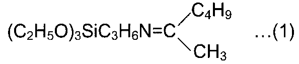
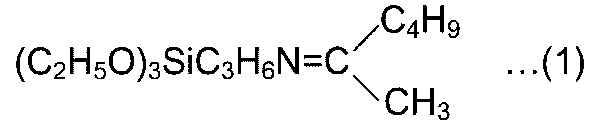
- the component (D) may be surface-treated with an aminosilane represented by the structural formula shown in the following formula (1).
- the component (B) may be contained in an amount of 0.5 equivalents to 1.8 equivalents with respect to 1 equivalent of the epoxy group of the component (A).
- the component (B) may be an acid anhydride curing agent, a phenol resin curing agent, or an amine curing agent.
- the component (A) may include at least one of bisphenol F type epoxy resin, bisphenol A type epoxy resin, naphthalene type epoxy resin, and aminophenol type epoxy resin.
- the component (E) is a butadiene elastomer, a silicone elastomer, an acrylic copolymer, a styrene butadiene elastomer, a butadiene / acrylonitrile / 2,3-epoxypropyl methacrylate / divinylbenzene copolymer, a butadiene It may contain at least one of acrylonitrile / methacrylic acid / divinylbenzene copolymer, amino group-terminated butadiene / acrylonitrile copolymer, and carboxyl group-terminated butadiene / acrylonitrile copolymer.
- This resin composition may be produced by mixing the component (C) with at least a part of the component (A) to produce a master batch and mixing the other components with the master batch.
- the present invention also provides a semiconductor encapsulant using the above-described epoxy resin composition.
- the semiconductor sealing agent may seal a conductive portion of a semiconductor device formed of two or more metals or alloys.
- the two or more metals or alloys are selected from Au, Ag, Cu, Sn, Pb, Ni, Pd, Co, Cd, Bi, In, Sb, and Zn, or It may be an alloy based on a metal.
- the conducting part of the semiconductor device to be sealed is two kinds of metals or alloys, and the cross section of the epoxy resin composition that sealed the conducting part is based on the boundary between the two kinds of metals or alloys.
- the filler dispersion index calculated by the following equation may be 50 or more and 150 or less by dividing into two regions and using the occupancy ratios of the component (C) and the component (D) in each region.
- Filler dispersion index 100 ⁇ (area Ra occupation ratio) / (area Rb occupation ratio)
- the present invention provides a semiconductor device using the above-described semiconductor sealing agent.
- the dispersion of the filler can be promoted by the present invention.
- FIG. 1 is a diagram for explaining evaluation of a dispersion index of a filler.
- FIG. 2 is an enlarged view of region II shown in FIG.
- the epoxy resin composition of the present invention includes (A) an epoxy resin, (B) a curing agent, (C) a small diameter silica filler, (D) a large diameter silica filler, and (E) an elastomer.
- component (A) examples include bisphenol F type epoxy resin, bisphenol A type epoxy resin, naphthalene type epoxy resin, aminophenol type epoxy resin, phenol novolac type epoxy resin, alicyclic epoxy resin, siloxane type epoxy resin, biphenyl type Examples thereof include epoxy resins, glycidyl ester type epoxy resins, glycidyl amine type epoxy resins, hydantoin type epoxy resins, and naphthalene ring-containing epoxy resins.
- the compounds exemplified here may be used alone or in combination of two or more.
- component (B) examples include an acid anhydride curing agent, a phenol resin curing agent, and an amine curing agent.
- component (B) It is preferable that 0.5 equivalent or more and 1.8 equivalent or less are contained with respect to 1 equivalent of epoxy groups of (A) component.
- Examples of the component (C) and the component (D) include amorphous silica, crystalline silica, fused silica, ground silica, and nano silica.
- the shape of the component (C) and the component (D) is not particularly limited, and may be any form of granular, powder, flakes, and the like.
- the average particle diameter of the silica filler in the present invention refers to a volume-based D50 (median diameter) measured by a laser diffraction method or a field emission scanning electron microscope (FE-SEM) regardless of the shape of the silica filler. .
- the average particle size of the component is preferably 10 nm or more and 100 nm or less.
- the epoxy resin composition of the present invention preferably contains 0.1% by mass or more and 10% by mass or less of component (C) and 47% by mass or more and 75% by mass or less of component (D). Furthermore, it is preferable that the epoxy resin composition of this invention contains 50.1 mass% or more and 77 mass% or less of (C) component and (D) component in total. More preferably, the total range of the component (C) and the component (D) is in the range of 52% by mass to 77% by mass.
- At least one of the component (C) and the component (D) may be surface-treated with a silane coupling agent.
- the silane coupling agent used for the surface treatment include various silane coupling agents such as epoxy, methacrylic, amino, vinyl, glycidoxy, and mercapto. Of these, aminosilane having a structure represented by the following formula (1) is preferably used for the surface treatment of the component (D).
- component (E) examples include butadiene elastomers, silicone elastomers, acrylic copolymers, styrene butadiene elastomers, butadiene / acrylonitrile / 2,3-epoxypropyl methacrylate / divinylbenzene copolymer, butadiene / acrylonitrile / methacrylic acid / Examples thereof include a divinylbenzene copolymer, an amino group-terminated butadiene / acrylonitrile copolymer, and a carboxyl group-terminated butadiene / acrylonitrile copolymer.
- the compound illustrated here may be used independently and 2 or more compounds may be mixed and used. That is, the component (E) may be an elastomer containing at least one of the above-described compounds. (E) It is preferable that 0.1 mass% or more and 8 mass% or less of component are contained.
- the epoxy resin composition includes an ion trap agent, a pigment, a dye, an antifoaming agent, a stress relaxation agent, and a pH adjusting agent.
- Additives such as accelerators, surfactants, and coupling agents may also be included.
- the epoxy resin composition is used as a semiconductor sealing agent (underfill agent) when an electronic device such as a semiconductor element is mounted by flip chip mounting or BGA (Ball Grid Array) / CSP (Chip Size Package).
- This epoxy resin composition may be used as an adhesive when an electronic device is bonded to a substrate or a package.
- a semiconductor element and a substrate are first joined.
- a semiconductor sealing agent is injected into the gap between the semiconductor element and the substrate.
- a semiconductor sealing agent is applied along the outer periphery of the semiconductor element.
- the semiconductor sealing agent spreads in the gap by capillary action. Therefore, the semiconductor encapsulant is preferably in a liquid state at the temperature at which this process is performed.
- the injected semiconductor encapsulant is thermally cured by heating (for example, 80 to 165 ° C.).
- FIG. 1 is a view illustrating a semiconductor device sealed with a semiconductor sealing agent according to the present invention.
- FIG. 1 shows an example of flip chip mounting using a metal pillar.
- FIG. 1 shows a cross section of the semiconductor device.
- An electrode 2 is formed on the substrate 1.
- An insulating film 3 is formed at a place other than the electrode 2.
- Solder bumps 4 are disposed on the electrodes 2.
- An electrode 7 is formed on the semiconductor chip 5 (downward in the figure). The entire semiconductor chip 5 is covered with a passivation 9. An opening is provided at a position corresponding to the electrode 7.
- a copper pillar 8 which is a kind of metal pillar is formed.
- the copper pillar 8 is made of copper (Cu) or an alloy mainly composed of copper.
- the solder bump 4 is made of an alloy mainly composed of tin (Sn).
- the materials for the solder bumps and the metal pillars are not limited to those exemplified here.
- Solder bumps and metal pillars are based on, for example, two or more metals selected from Au, Ag, Cu, Sn, Pb, Ni, Pd, Co, Cd, Bi, In, Sb, and Zn, or based on the metals. Formed of an alloy.
- the semiconductor sealing agent according to this embodiment is used for sealing a conductive portion of a semiconductor device in which the conductive portion is formed of two or more kinds of metals or an alloy based on the metal.
- the epoxy resin composition is produced by, for example, stirring, melting, mixing, or dispersing the components (A) to (E) and other additives simultaneously or separately, with heat treatment if necessary.
- the These methods such as mixing, stirring, and dispersion are not particularly limited.
- a laika machine equipped with a stirring and heating device, a three-roll mill, a ball mill, a planetary mixer, a bead mill, or the like can be used. Moreover, you may use combining these apparatuses. Here, you may prepare a masterbatch by mixing (A) component and (C) component.
- An epoxy resin composition can be produced by mixing the obtained master batch with other components.
- Tables 1 to 10 show the compositions of the epoxy resin compositions used as sealants in Examples 1 to 37 and Comparative Examples 1 to 9. These tables also show the evaluation results of the epoxy resin composition as a sealant, which will be described later.
- the composition of the epoxy resin composition is expressed in parts by mass (corresponding to mass% since the total of parts by mass is 100), excluding the equivalence ratio.
- the component (A) in the table at least one of the epoxy resins a1 to a5 was used.
- the epoxy resin a1 YDF8170 manufactured by Nippon Steel & Sumikin Chemical Co., Ltd., which is a kind of bisphenol F type epoxy resin
- the epoxy resin a2, 850CRP manufactured by DIC Corporation which is a kind of bisphenol A type epoxy resin
- the epoxy resin a3, HP-4032D manufactured by DIC Corporation which is a kind of naphthalene type epoxy resin
- the epoxy resin a4, jer630 manufactured by Mitsubishi Chemical Corporation which is a kind of aminophenol type epoxy resin, was used.
- the curing agent b1 to b5 As the component (B) in the table, at least one of the curing agents b1 to b5 was used.
- the curing agent b1 Kayahard AA manufactured by Nippon Kayaku Co., Ltd., which is an amine curing agent, was used.
- the curing agent b2 EH105L manufactured by Adeka Corporation, which is an amine curing agent, was used.
- MEH-8005 manufactured by Meiwa Kasei Co., Ltd., which is a phenol resin curing agent, was used.
- any of YA010C (average particle size: 10 nm), YA050C (average particle size: 50 nm), and YC100C (average particle size: 100 nm) manufactured by Admatechs Co., Ltd. is used. It was.
- the average particle diameter of the filler is a median diameter (D50).
- the average particle diameter is a value measured by a field emission scanning electron microscope (FE-SEM).
- 0.2 ⁇ m high average particle size: 0.2 ⁇ m
- SE-1050 average particle size: 0.3 ⁇ m
- Admatechs Co., Ltd. SE Any of -2300 (average particle size: 0.6 ⁇ m), SE-4050 (average particle size: 1 ⁇ m), and SE-6050 (average particle size: 2 ⁇ m) were used.
- the average particle diameter is a median diameter (D50).
- the average particle diameter is a value measured by a laser diffraction / scattering particle size distribution meter.
- any of the surface treatment agents f1 to f3 was used as the surface treatment agent for the component (D).
- As the surface treatment agent f1 KBM403 (3-glycidoxypropyltrimethoxysilane) manufactured by Shin-Etsu Chemical Co., Ltd. was used.
- As the surface treatment agent f2 KBM503 (3-methacryloxypropyltrimethoxysilane) manufactured by Shin-Etsu Chemical Co., Ltd. was used.
- KBE9103 3-triethoxysilyl-N- (1,3-dimethyl-butylidene) propylamine, compound of formula (1)) manufactured by Shin-Etsu Chemical Co., Ltd. was used.
- elastomer e1 to e9 As the component (E) in the table, at least one of the elastomers e1 to e9 was used.
- elastomer e1 MX137 manufactured by Kaneka Corporation, which is a kind of butadiene elastomer, was used.
- elastomer e2 MX965 manufactured by Kaneka Corporation, which is a kind of silicone elastomer, was used.
- elastomer e4 M52N manufactured by ARKEMA, which is a kind of acrylic copolymer, was used.
- elastomer e5 As the elastomer e5, XER-81 manufactured by JSR Corporation, which is a kind of butadiene / acrylonitrile / 2,3 epoxypropyl methacrylate / divinylbenzene copolymer, was used.
- elastomer e6 As the elastomer e6, XER-91 manufactured by JSR Corporation, which is a kind of butadiene / acrylonitrile / methacrylic acid / divinylbenzene copolymer, was used.
- elastomer e7 ATBN manufactured by Ube Industries, Ltd., which is a kind of an amino group-terminated butadiene / acrylonitrile copolymer, was used.
- elastomer e8 CTBN manufactured by Ube Industries, Ltd., which is a kind of a carboxyl group-terminated butadiene / acrylonitrile copolymer, was used.
- elastomer e9 KMP-605 manufactured by Shin-Etsu Silicone Co., Ltd., which is a kind of silicone elastomer, was used.
- FIG. 2 is a diagram illustrating a cross-sectional photograph of a semiconductor device. This figure is a cross-sectional photograph of the region (region II) indicated by “II” in FIG.
- a region II in FIG. 1 includes a cross section of the underfill agent 10 that has been poured into the space sandwiched between the wiring substrate 1, the chip substrate 5, the copper pillar 8, and the solder 4 and then cured. This region II was photographed using a scanning electron microscope (SEM) or the like. The captured image is analyzed by a computer by image processing software as follows. That is, first, an area of the underfill agent 10 in the photographed image is designated by the user or the like.
- SEM scanning electron microscope
- Binarization processing is performed with the median value of the specified luminance distribution in that region as a reference.
- the white portion indicates the filler
- the black portion indicates the resin component other than the filler.
- the designated region is divided into two regions, a region Ra on the copper pillar 8 side and a region Rb on the solder 4 side, with an extension of the boundary line L between the copper pillar 8 and the solder 4 as a boundary.
- the occupancy rate of the silica filler in each region is calculated.
- the dispersion index indicates that the filler is uniformly distributed in each region when the dispersion index is 100.
- the dispersion index is smaller than 100, it indicates that the filler is biased toward the region Rb.
- the dispersion index is small, it indicates that the filler is largely biased to the region Rb.
- the dispersion index increases and approaches 100, it indicates that the filler distribution is approaching a more uniform state.
- the dispersion index was 50 or less, the uniformity of the filler distribution of the sample was judged to be poor.
- ImageJ ImageJ of the National Institutes of Health
- TI Thixotropic Index
- Table 1 shows the compositions of the epoxy resin compositions of Examples 1 to 5 and Comparative Examples 1 and 2, and the evaluation results.
- surface the composition of an epoxy resin composition is represented by the mass part (mass%).
- Table 1 shows an example in which the content of the component (E) is changed.
- Comparative Example 1 not including any of the component (C) and the component (E)
- the dispersion index was 38.
- Examples 1 to 5 including the component (C) and the component (E) the dispersion index was 50 or more.
- the content of component (E) increased, the dispersion index approached 100. That is, when the content of the component (E) is increased, the uniformity of the filler distribution is improved.
- the content of the component (E) was 8.3% by mass (Comparative Example 2), a defect occurred in the injection property test.
- Table 2 shows the compositions of the epoxy resin compositions of Examples 3 and 6 to 13 and the evaluation results. Table 2 shows an example in which the type of component (E) changes. Even if any of the elastomers e1 to e9 is used as the component (E), the uniformity of the filler distribution is improved.
- Table 3 shows the compositions of the epoxy resin compositions of Examples 3 and 14 to 16 and Comparative Examples 3 and 4, and the results of evaluation.
- Table 3 shows an example in which the content of the component (C) is changed.
- the content of component (C) was 0.05% by mass (Comparative Example 3)
- the dispersion index was 44, and the uniformity of the filler distribution was poor.
- the content of the component (C) is preferably 0.1% by mass or more.
- the viscosity was 132 Pa ⁇ s. Therefore, it is preferable that content of (C) component is 10 mass% or less from a viewpoint of the moderate viscosity as a sealing agent.
- Table 4 shows the compositions of the epoxy resin compositions of Examples 3, 17, 18 and Comparative Example 5, and the results of evaluation. Table 4 shows an example in which the average particle size of the component (C) is changed.
- component (D) having an average particle size of 0.2 ⁇ m (that is, 200 nm) is used instead of component (C).
- component (C) is not included (Comparative Example 5)
- a defect occurs in the dispersion index.
- the dispersion index is improved.
- the dispersion index is further improved as the average particle size of the component (C) becomes smaller. That is, the dispersion index improved when the average particle size of the component (C) was in the range of 10 to 100 nm.
- Table 5 shows the compositions of the epoxy resin compositions of Examples 3, 19, 20 and Comparative Example 6, and the results of evaluation.
- Table 5 shows an example in which the average particle diameter of the component (D) is changed.
- the average particle size of component (D) was in the range of 0.2 to 2 ⁇ m, no defects were observed in the dispersion index test. The dispersion index improves as the average particle size of component (D) decreases. Conversely, the viscosity gets worse.
- the average particle size of component (D) was 0.2 ⁇ m (Comparative Example 6)
- a high viscosity of 195 Pa ⁇ s was exhibited. Therefore, from the viewpoint of moderate viscosity as a sealant, the average particle size of the component (D) is preferably 0.3 ⁇ m or more.
- Table 6 shows the compositions of the epoxy resin compositions of Examples 3, 21 to 24 and Comparative Examples 7 to 9, and the results of evaluation.
- Table 6 shows an example in which the content of the component (D) is changed.
- the content of component (D) was in the range of 52 to 75% by mass, the dispersion index improved.
- the injectability deteriorated as the content of the component (D) increased.
- the content of component (D) is preferably 75% or less from the viewpoint of moderate injectability as a sealant.
- Table 7 shows the compositions of the epoxy resin compositions of Examples 3 and 25 to 27 and the evaluation results. Table 7 shows an example in which the surface treatment of the component (D) is changed. Even if the component (D) is surface-treated with a silane coupling agent having any one of an epoxy group, a methacryl group and an amino group, and is not surface-treated, it is poor in the dispersion index test. Did not occur.
- Table 8 shows the compositions of the epoxy resin compositions of Examples 3, 28 and 29 and the results of evaluation. Table 8 shows an example in which the equivalent ratio of the component (B) to the component (A) is changed. When the equivalent ratio of the component (B) to 1 equivalent of the epoxy group (A) was in the range of 0.5 equivalents to 1.8 equivalents, no failure occurred in the dispersion index test.
- Table 9 shows the compositions of the epoxy resin compositions of Examples 3 and 30 to 33 and the evaluation results. Table 9 shows an example in which the type of component (A) and the content ratio of component (A) to component (B) are changed. When the component (A) was any of the epoxy resins a1 to a5, no defect was observed in the dispersion index test.
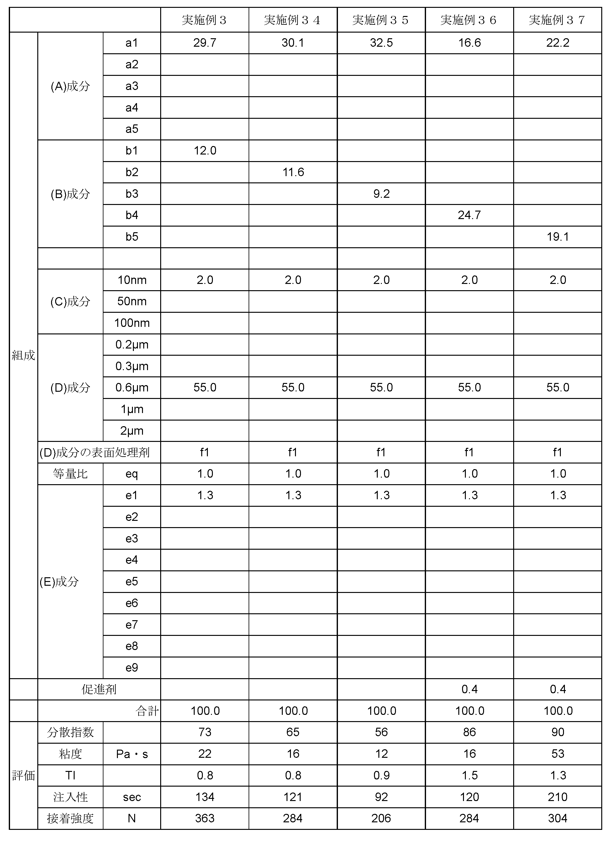
- Table 10 shows the compositions of the epoxy resin compositions of Example 3 and Examples 34 to 37 and the evaluation results. Table 10 shows an example in which the type of component (B) and the content ratio of component (A) to component (B) are changed. When the component (B) was any of the curing agents b1 to b5, no defect occurred in the dispersion index test.
- epoxy resin composition according to the present invention may be the following first to eighth epoxy resin compositions.
- the first epoxy resin composition comprises (A) an epoxy resin, (B) a curing agent, (C) 0.1 to 10% by mass of a silica filler having an average particle diameter of 10 nm to 100 nm, and (D 47) to 75% by mass of a silica filler having an average particle size of 0.3 ⁇ m or more and 2 ⁇ m or less, and (E) 0.1 to 8% by mass of an elastomer, the component (C) and the component (D) Is an epoxy resin composition characterized by containing 47.1 to 77% by mass in total.
- the second epoxy resin composition is the first epoxy resin composition, wherein at least one of the component (C) and the component (D) is surface-treated with a silane coupling agent. .
- the third epoxy resin composition is the first or second epoxy resin composition, wherein the component (D) is surface-treated with an aminosilane having a structure represented by the following formula (1): .
- the fourth to third epoxy resins may comprise 0.5 to 1.8 equivalents of the component (B) with respect to 1 equivalent of the epoxy group of the component (A). Any one of the epoxy resin compositions.
- the fifth epoxy resin composition is characterized in that the component (B) is an acid anhydride curing agent, a phenol resin curing agent, or an amine curing agent. It is a composition.
- the component (A) contains at least one of bisphenol F type epoxy resin, bisphenol A type epoxy resin, naphthalene type epoxy resin, and aminophenol type epoxy resin.
- the epoxy resin composition according to any one of the first to fifth aspects.
- the above-mentioned first product comprising at least one of a polymer, a butadiene / acrylonitrile / methacrylic acid / divinylbenzene copolymer, an amino group-terminated butadiene / acrylonitrile copolymer, and a carboxyl group-terminated butadiene / acrylonitrile copolymer.
- the epoxy resin composition according to any one of 6 to 6.
- the eighth epoxy resin composition at least a part of the (A) epoxy resin is mixed with the silica filler (C) having an average particle diameter of 10 to 100 nm to produce a master batch,
- the epoxy resin composition according to any one of the first to seventh aspects, which is produced by mixing components.
- the semiconductor sealing agent according to the present invention may be the following first to fourth semiconductor sealing agents.
- the first semiconductor encapsulant is a semiconductor encapsulant using any one of the first to eighth epoxy resin compositions.
- the second semiconductor encapsulant is the first semiconductor encapsulant characterized in that the conductive portion of the semiconductor device to be sealed is two or more metals or alloys.
- the conductive portion of the semiconductor device to be sealed is selected from Au, Ag, Cu, Sn, Pb, Ni, Pd, Co, Cd, Bi, In, Sb, and Zn.
- the second semiconductor encapsulant is formed of two or more metals or an alloy based on the metal.
- the conductive part of the semiconductor device to be sealed is two kinds of metals or alloys
- the cross section of the epoxy resin composition sealing the conductive part is the two kinds of
- the filler dispersion index is divided into two regions along the boundary of the metal or alloy, and the filler dispersion index calculated according to the ratio of the areas of the (C) component and the (D) component in each region is 50 or more and 150 or less. This is the first semiconductor sealing agent.
- the semiconductor device according to the present invention is a semiconductor device using any one of the first to fourth semiconductor encapsulants.
Landscapes
- Chemical & Material Sciences (AREA)
- Health & Medical Sciences (AREA)
- Chemical Kinetics & Catalysis (AREA)
- Medicinal Chemistry (AREA)
- Polymers & Plastics (AREA)
- Organic Chemistry (AREA)
- Compositions Of Macromolecular Compounds (AREA)
- Epoxy Resins (AREA)
- Processes Of Treating Macromolecular Substances (AREA)
- Structures Or Materials For Encapsulating Or Coating Semiconductor Devices Or Solid State Devices (AREA)
Abstract
Description
本願は、2013年11月29日に出願された日本特許出願「特願2013-247567」に基づく優先権を主張すると共に、参照によりその内容を組み込む。

フィラー分散指数=100×(領域Raの占有率)/(領域Rbの占有率)

表1~10は、実施例1~37および比較例1~9で、封止剤として用いられたエポキシ樹脂組成物の組成を示す。また、これらの表は、後述する、封止剤としてのエポキシ樹脂組成物の評価結果をも示す。表1~10において、エポキシ樹脂組成物の組成は、等量比を除いて、質量部(質量部の合計が100なので質量%に相当)で表されている。
実施例1~37および比較例1~9で用いられたエポキシ樹脂組成物を試料として、以下の評価を行った。
図2は、半導体装置の断面写真を例示する図である。この図は、図1に「II」で示された領域(領域II)の断面写真である。図1の領域IIには、配線基板1、チップ基板5、銅ピラー8、およびハンダ4に挟まれた空間に流し込まれたのち、硬化したアンダーフィル剤10の断面が含まれる。この領域IIを走査型電子顕微鏡(SEM)などを用いて撮影した。その撮影画像を、画像処理ソフトウェアによって、以下のようにコンピュータにより分析する。すなわち、まず、この撮影画像のうち、アンダーフィル剤10の領域がユーザなどによって指定される。指定されたその領域の輝度分布の中央値を基準として、二値化処理が行われる。ここで、二値化された画像のうち、白い部分がフィラーを示しており、黒い部分がフィラー以外の樹脂成分を示している。次に、指定された領域は、銅ピラー8とハンダ4との境界線Lの延長線を境として、銅ピラー8側の領域Ra、およびハンダ4側の領域Rbの2つに区画される。そして、銅ピラー8側の領域Ra、およびハンダ4側の領域Rbの各画像に基づいて、それぞれの領域中のシリカフィラーの占有率が算出される。分散指数は次式によって算出される。
分散指数=100×(領域Raの占有率)/(領域Rbの占有率)
ブルックフィールド回転粘度計を用いて、50rpmで、25℃における、上記エポキシ樹脂組成物の粘度を測定した。
5rpmおよび50rpmで、上記エポキシ樹脂組成物の粘度を測定した。測定された5rpmにおける粘度の値を50rpmにおける粘度の値で除した値をTI値とした。
110℃において、20μmのギャップ(間隙)に評価用試料を注入した。注入された評価用試料が入口から20mmの位置に到達するまでの時間を測定した。到達までの時間が短いほど注入性が良いことを示している。なお、表中の注入性の欄にある「-」の記載は、評価用試料が20mmの位置まで到達しなかったこと(すなわち不良であること)を意味する。
FR-4上に評価用試料を約0.5mgポッティングした。この上に2mm角シリコンチップを載せ、室温で5分間放置した。その後、送風乾燥機を用いて、150℃で120分の条件で、評価用試料を硬化させた。このようにして得られた試験片について、接着強度を卓上型強度測定機(アイコーエンジニアリング株式会社製1605HTP)を用いて測定した。なお、10回の測定により得られた測定値の平均値を検査値とした。
(3-1)エラストマー量について
表1は、実施例1~5、並びに比較例1および2のエポキシ樹脂組成物の組成、並びに評価の結果を示す。以下、表において、エポキシ樹脂組成物の組成は質量部(質量%)で表されている。表1は、(E)成分の含有量が変化している例を示している。(C)成分および(E)成分のうちのいずれをも含まない比較例1では、分散指数が38であった。一方、(C)成分および(E)成分を含む実施例1~5では、分散指数が50以上となった。(E)成分の含有量が増えると、分散指数が100に近づいていった。すなわち、(E)成分の含有量が増えると、フィラー分布の均一性が改善された。ただし、(E)成分の含有量が8.3質量%(比較例2)になると注入性試験で不良が発生した。
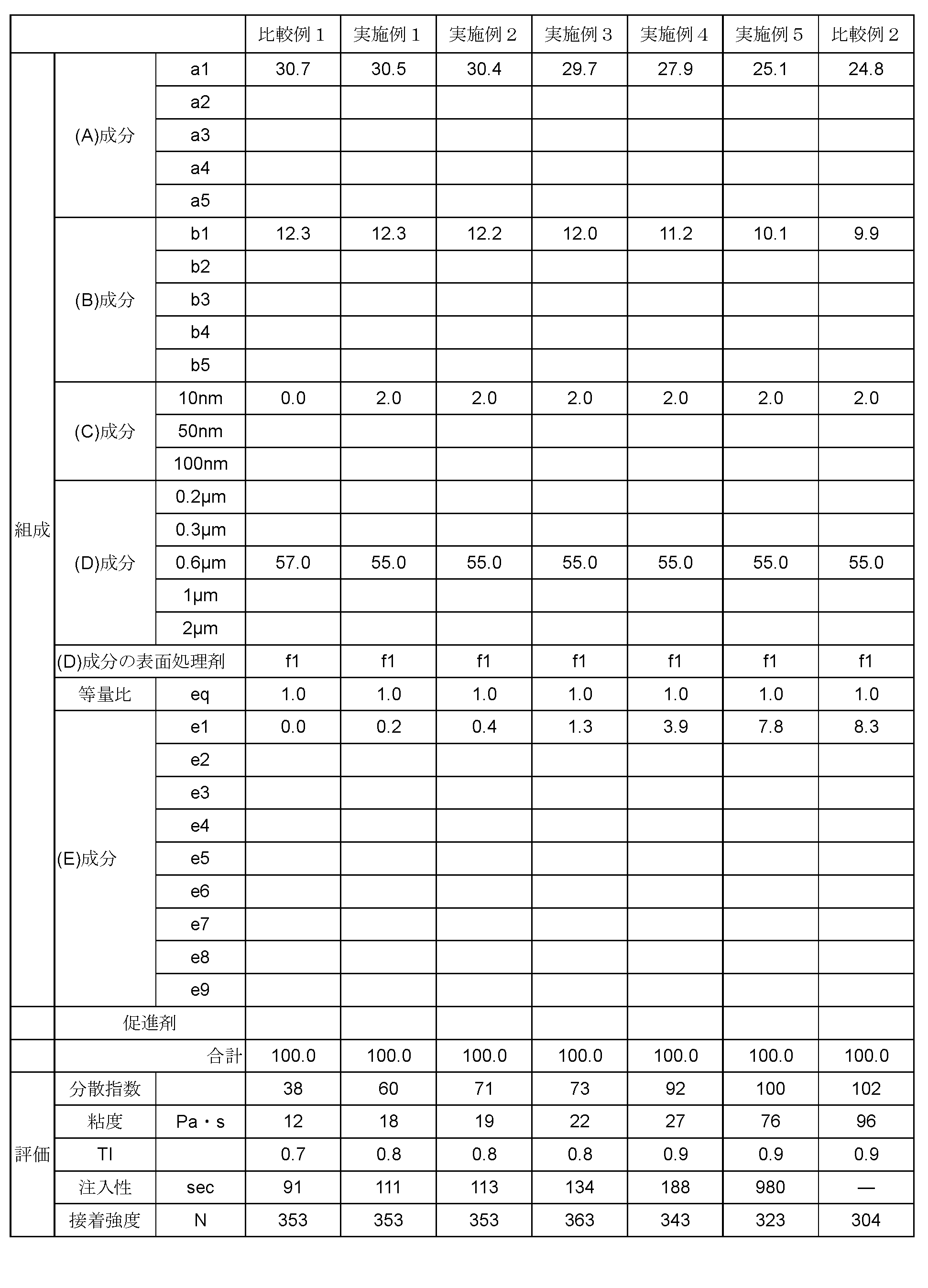
表2は、実施例3および6~13のエポキシ樹脂組成物の組成、並びに評価の結果を示す。表2は、(E)成分の種類が変化している例を示している。(E)成分としてエラストマーe1~e9のいずれを用いても、フィラー分布の均一性が改善されている。
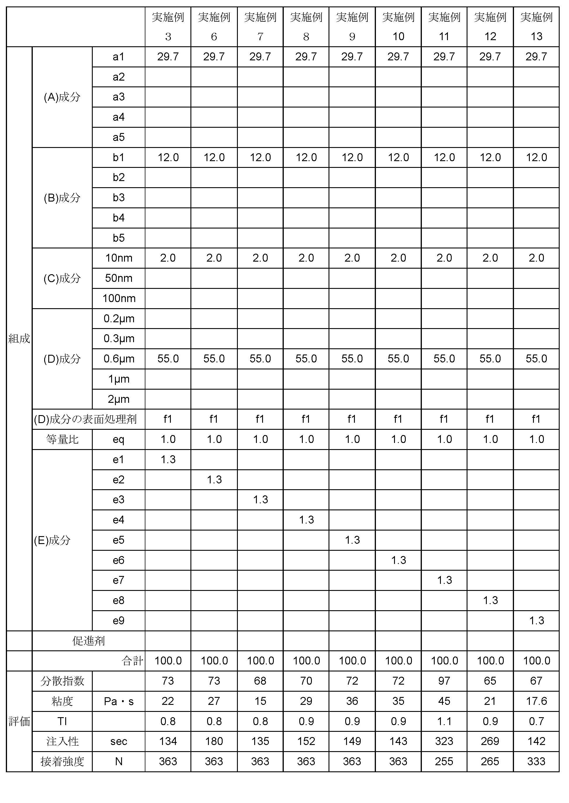
表3は、実施例3および14~16、並びに比較例3および4のエポキシ樹脂組成物の組成、並びに評価の結果を示す。表3は、(C)成分の含有量が変化している例を示している。(C)成分の含有量が0.05質量%(比較例3)だと、分散指数が44であり、フィラー分布の均一性が不良であった。(C)成分の含有量が増えると、分散指数が100に近づいていき、フィラー分布の均一性が改善された。したがって、(C)成分の含有量は0.1質量%以上であることが好ましい。ただし、(C)成分の含有量が11質量%になると、粘度が132Pa・sとなった。よって、封止剤としての適度な粘度の観点から(C)成分の含有量は10質量%以下であることが好ましい。
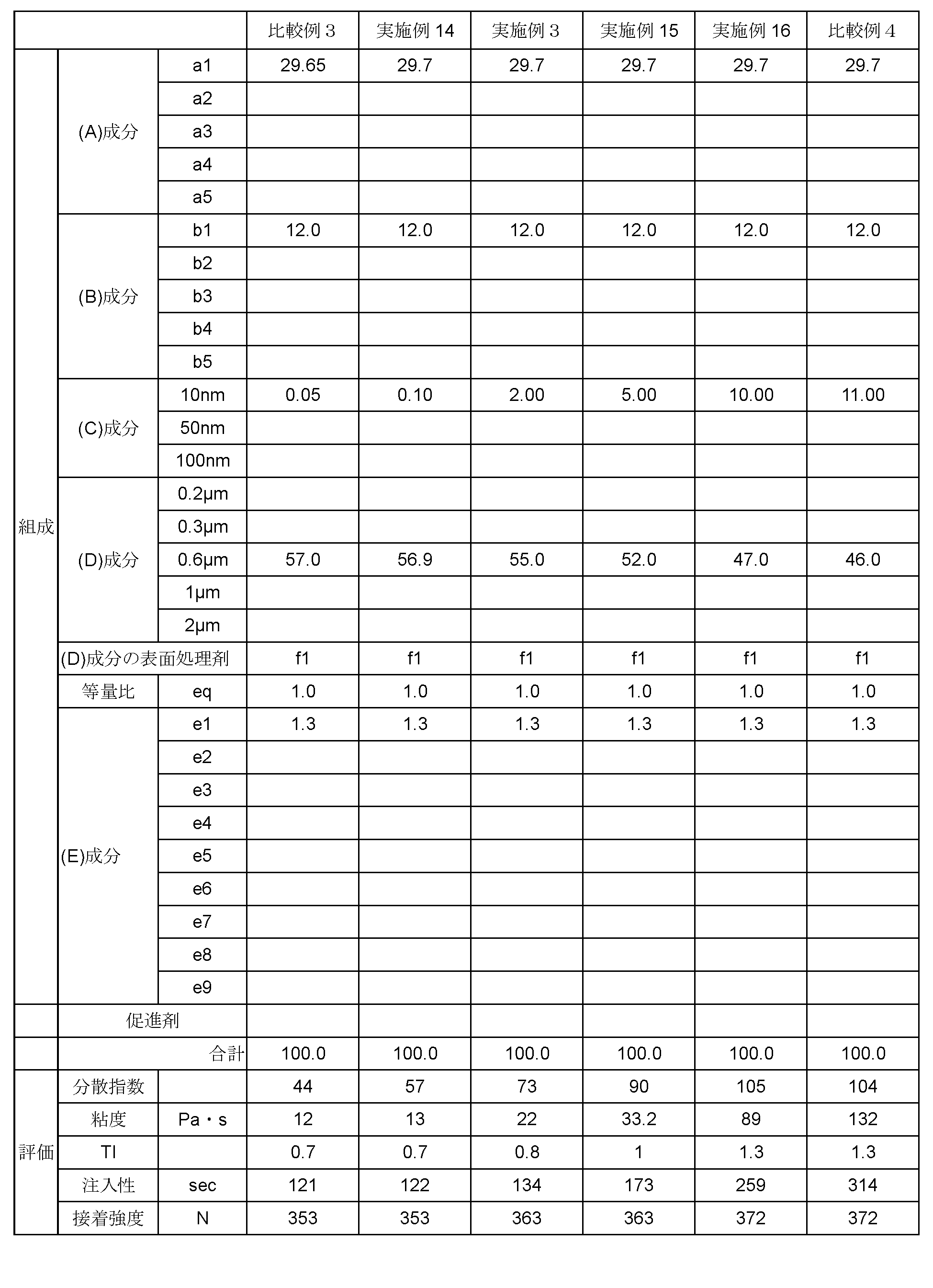
表4は、実施例3,17,18および比較例5のエポキシ樹脂組成物の組成、並びに評価の結果を示す。表4は、(C)成分の平均粒径が変化している例を示している。なお比較例5においては、(C)成分の代わりに平均粒径0.2μm(すなわち200nm)の(D)成分を用いている。(C)成分が含まれない場合(比較例5)、分散指数で不良が発生する。(C)成分が含まれると、分散指数が改善する。このとき、(C)成分の平均粒径が小さくなるほど、分散指数がより改善する。すなわち、(C)成分の平均粒径が10~100nmの範囲で、分散指数が改善した。
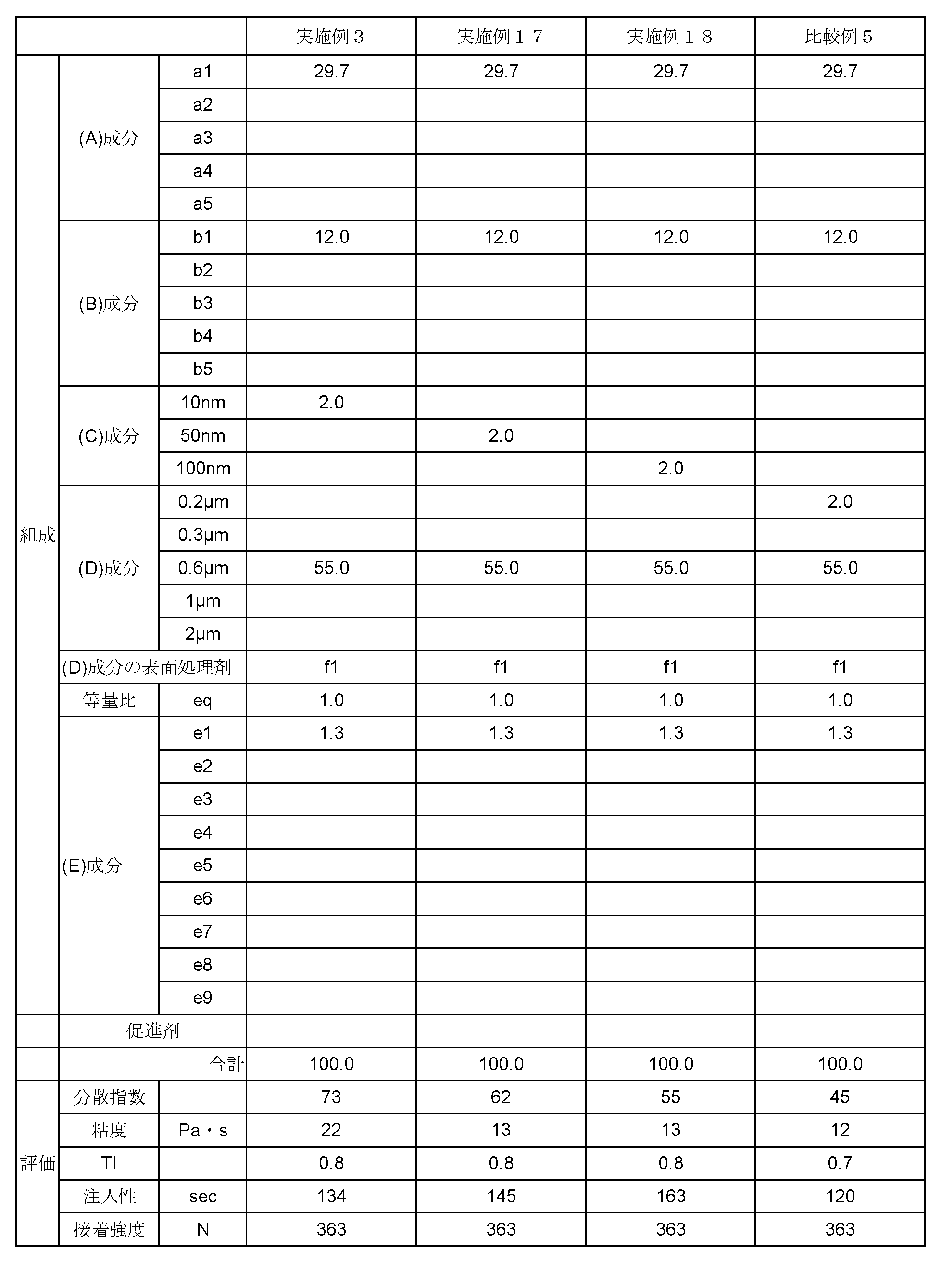
表5は、実施例3,19,20および比較例6のエポキシ樹脂組成物の組成、並びに評価の結果を示す。表5は、(D)成分の平均粒径が変化している例を示している。(D)成分の平均粒径が0.2~2μmの範囲では、分散指数試験で不良は観測されなかった。(D)成分の平均粒径が小さくなるにつれ分散指数は改善する。逆に、粘度は悪化する。(D)成分の平均粒径が0.2μm(比較例6)のとき、195Pa・sの高い粘度を示した。したがって封止剤としての適度な粘度の観点から、(D)成分の平均粒径は0.3μm以上であることが好ましい。

表6は、実施例3、21~24および比較例7~9のエポキシ樹脂組成物の組成、並びに評価の結果を示す。表6は、(D)成分の含有量が変化している例を示している。(D)成分の含有量が52~75質量%の範囲では分散指数が改善した。しかし、(D)成分の含有量が多くなると注入性が悪化した。特に、(D)成分の含有量が76質量%(比較例9)になると、注入性試験で不良が観測された。したがって、封止剤としての適度な注入性の観点から、(D)成分の含有量は75%以下であることが好ましい。 なお、(C)成分の含有量と、(D)成分の含有量と、の合計が50.1質量%よりも少ない場合(比較例7および8)、エポキシ樹脂組成物の分散指数の値が50よりも小さくなることが確認された。
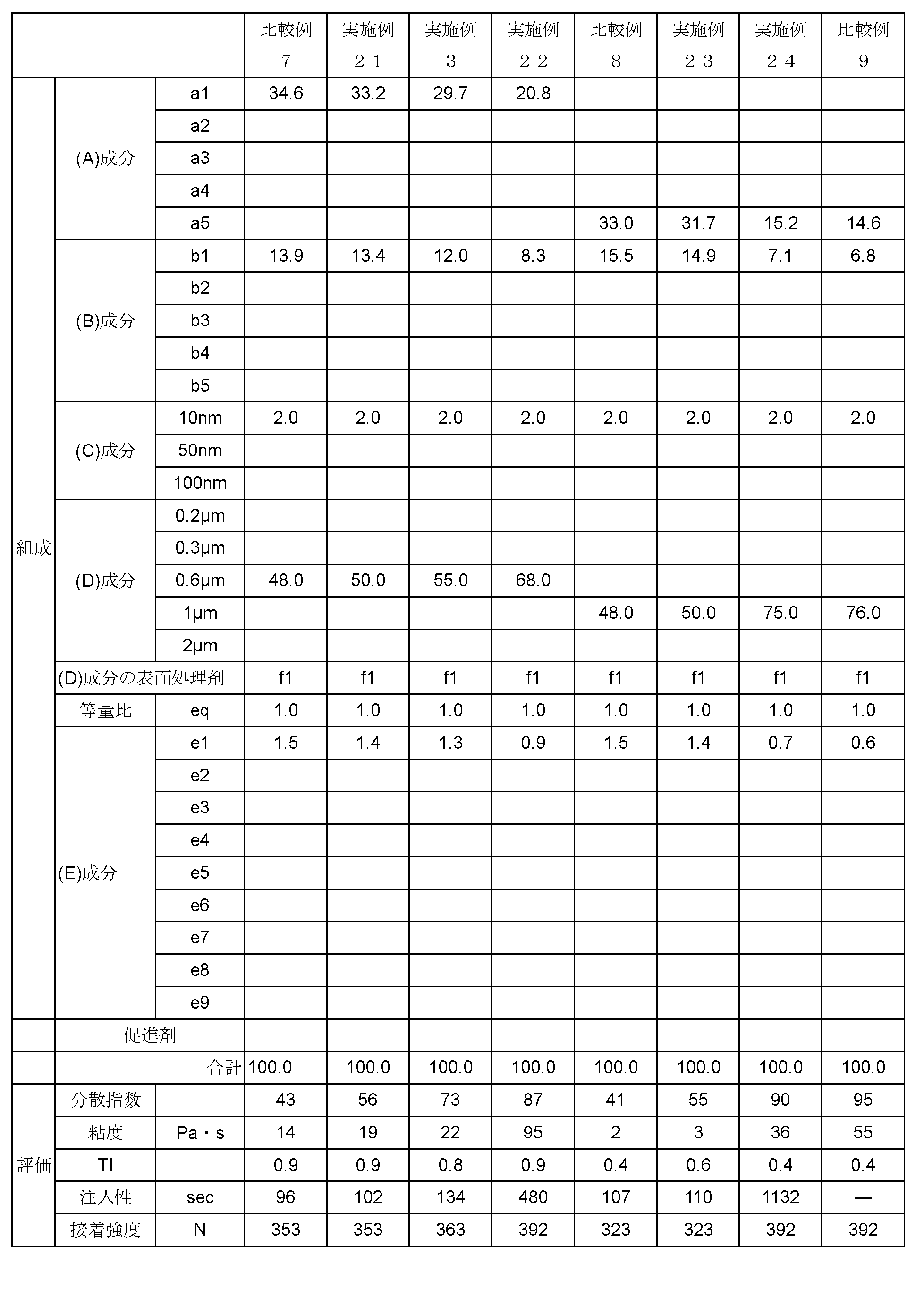
表7は、実施例3および25~27のエポキシ樹脂組成物の組成、並びに評価の結果を示す。表7は、(D)成分の表面処理が変化している例を示している。(D)成分が、エポキシ基、メタクリル基、およびアミノ基のうちのいずれかを有するシランカップリング剤を用いて表面処理されても、また、表面処理されていなくても、分散指数試験で不良は発生しなかった。
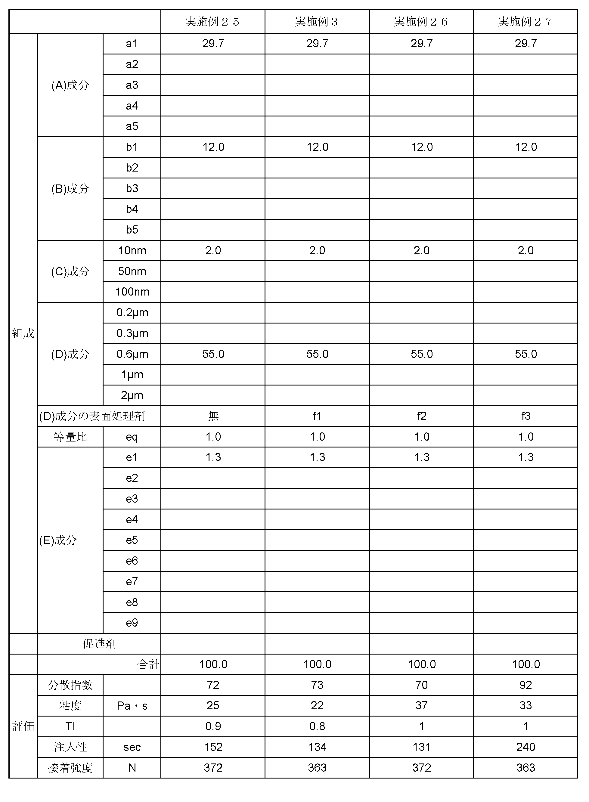
表8は、実施例3、28および29のエポキシ樹脂組成物の組成、並びに評価の結果を示す。表8は、(A)成分に対する(B)成分の当量比が変化している例を示している。(A)成分のエポキシ基1当量に対する(B)成分の当量比が0.5当量以上1.8当量以下の範囲で、分散指数試験に不良は発生しなかった。

表9は、実施例3および30~33のエポキシ樹脂組成物の組成、並びに評価の結果を示す。表9は、(A)成分の種類、および、(A)成分と(B)成分との含有比が変化している例を示している。(A)成分がエポキシ樹脂a1~a5のうちのいずれであっても、分散指数試験で不良は観測されなかった。
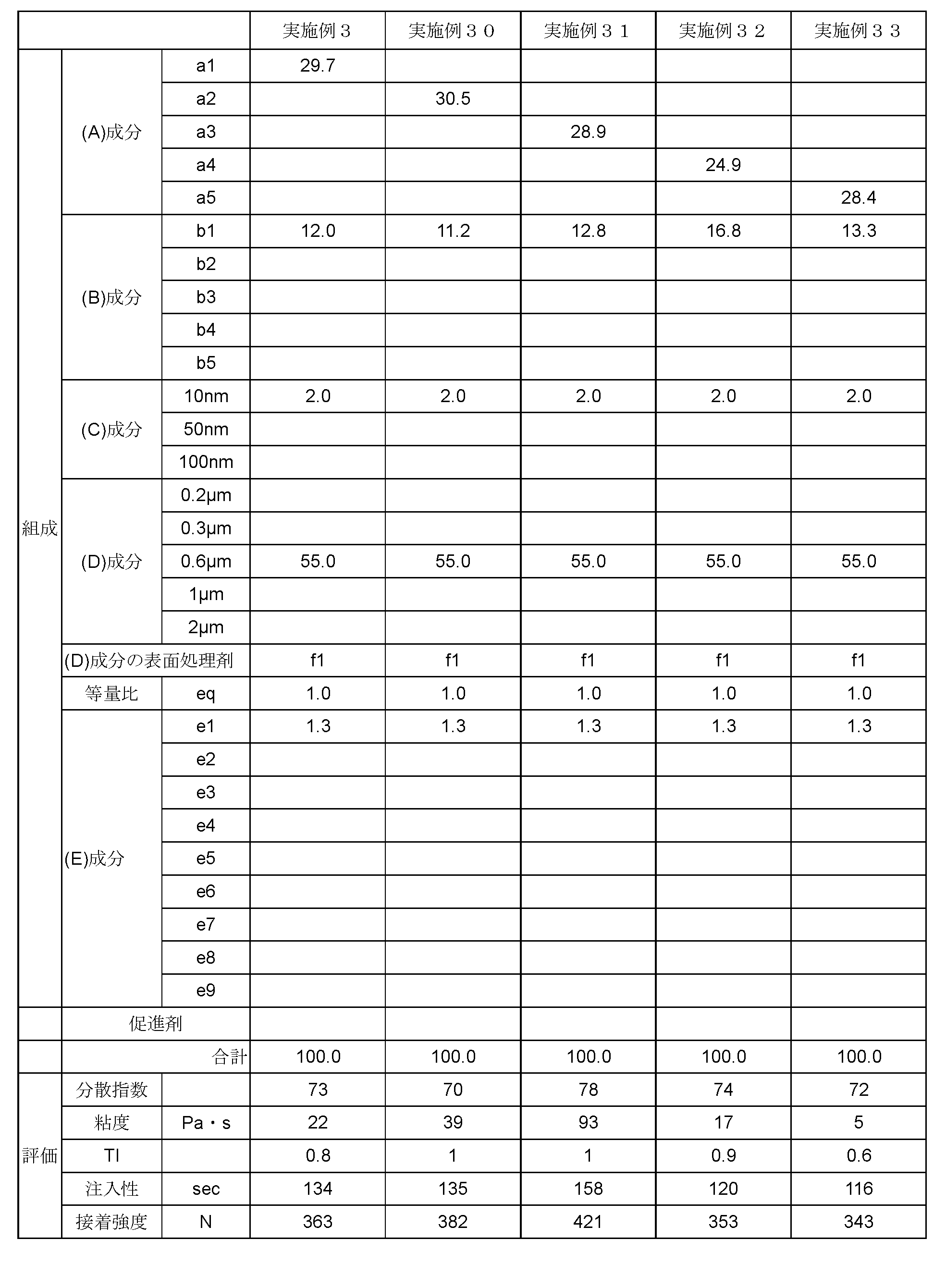
表10は、実施例3、および実施例34~37のエポキシ樹脂組成物の組成、並びに評価の結果を示す。表10は、(B)成分の種類、および、(A)成分と(B)成分との含有比が変化している例を示している。(B)成分が硬化剤b1~b5のうちのいずれであっても、分散指数試験で不良は発生しなかった。
Claims (13)
- (A)エポキシ樹脂と、
(B)硬化剤と、
(C)0.1~10質量%の、平均粒径10nm以上100nm以下のシリカフィラーと、
(D)47~75質量%の、平均粒径0.3μm以上2μm以下のシリカフィラーと、
(E)0.1~8質量%のエラストマーと
を含み、
前記(C)成分および前記(D)成分を、合計で50.1~77質量%含む
ことを特徴するエポキシ樹脂組成物。 - 前記(C)成分および前記(D)成分のうちの少なくとも一方が、シランカップリング剤で表面処理されている
ことを特徴とする請求項1に記載のエポキシ樹脂組成物。 - 前記(D)成分が、次式(1)に示す構造式で表されるアミノシランにより、表面処理されている
ことを特徴とする請求項1または2に記載のエポキシ樹脂組成物。
- 前記(A)成分のエポキシ基1当量に対し、前記(B)成分が、0.5~1.8当量含まれる
ことを特徴とする請求項1または2に記載のエポキシ樹脂組成物。 - 前記(B)成分が、酸無水物硬化剤、フェノール樹脂硬化剤、またはアミン硬化剤である
ことを特徴とする請求項1または2に記載のエポキシ樹脂組成物。 - 前記(A)成分が、ビスフェノールF型エポキシ樹脂、ビスフェノールA型エポキシ樹脂、ナフタレン型エポキシ樹脂、アミノフェノール型エポキシ樹脂のうちの少なくとも一つを含む
ことを特徴とする請求項1または2に記載のエポキシ樹脂組成物。 - 前記(E)成分が、ブタジエン系エラストマー、シリコーン系エラストマー、アクリルコポリマー、スチレンブタジエン系エラストマー、ブタジエン・アクリロニトリル・2,3-エポキシプロピルメタクリラート・ジビニルベンゼン共重合物、ブタジエン・アクリロニトリル・メタクリル酸・ジビニルベンゼン共重合物、アミノ基末端ブタジエン・アクリロニトリル共重合物、およびカルボキシル基末端ブタジエン・アクリロニトリル共重合物、のうちの少なくとも一つを含む
ことを特徴とする請求項1または2に記載のエポキシ樹脂組成物。 - 前記(A)成分の少なくとも一部に前記(C)成分を混合することにより、マスターバッチを生成し、当該マスターバッチに他の成分を混合して製造される
ことを特徴とする請求項1または2のいずれか一項に記載のエポキシ樹脂組成物。 - 請求項1ないし8のいずれか一項に記載のエポキシ樹脂組成物を用いた半導体封止剤。
- 2種以上の金属または合金により形成された、半導体装置の導通部分を封止する
ことを特徴とする請求項9に記載の半導体封止剤。 - 前記2種以上の金属または合金が、Au,Ag,Cu,Sn,Pb,Ni,Pd,Co,Cd,Bi,In,Sb,およびZnのうちから選択される、2種以上の金属または当該金属を基にする合金である
ことを特徴とする請求項10に記載の半導体封止剤。 - 封止する前記半導体装置の導通部分が、2種の金属または合金であり、
前記導通部分を封止した前記エポキシ樹脂組成物の断面を、前記2種の金属または合金の間の境界に基づいて2つの領域に区画し、当該各領域における前記(C)成分および前記(D)成分の占有率を用いて、次式により算出されるフィラー分散指数が50以上150以下である
ことを特徴とする請求項10に記載の半導体封止剤。
フィラー分散指数=100×(領域Raの占有率)/(領域Rbの占有率) - 請求項9ないし12のいずれか一項に記載の半導体封止剤を用いた半導体装置。
Priority Applications (5)
| Application Number | Priority Date | Filing Date | Title |
|---|---|---|---|
| KR1020167010979A KR102197928B1 (ko) | 2013-11-29 | 2014-11-28 | 에폭시 수지 조성물, 반도체 봉지제 및 반도체 장치 |
| JP2015550571A JP6475168B2 (ja) | 2013-11-29 | 2014-11-28 | エポキシ樹脂組成物、半導体封止剤および半導体装置 |
| US15/039,231 US10196513B2 (en) | 2013-11-29 | 2014-11-28 | Epoxy resin composition, semiconductor sealing agent, and semiconductor device |
| MYPI2016701410A MY185884A (en) | 2013-11-29 | 2014-11-28 | Epoxy resin composition, semiconductor sealing agent, and semiconductor device |
| CN201480058369.6A CN105658727B (zh) | 2013-11-29 | 2014-11-28 | 环氧树脂组合物、半导体密封剂及半导体装置 |
Applications Claiming Priority (2)
| Application Number | Priority Date | Filing Date | Title |
|---|---|---|---|
| JP2013-247567 | 2013-11-29 | ||
| JP2013247567 | 2013-11-29 |
Publications (1)
| Publication Number | Publication Date |
|---|---|
| WO2015079708A1 true WO2015079708A1 (ja) | 2015-06-04 |
Family
ID=53198670
Family Applications (1)
| Application Number | Title | Priority Date | Filing Date |
|---|---|---|---|
| PCT/JP2014/005967 Ceased WO2015079708A1 (ja) | 2013-11-29 | 2014-11-28 | エポキシ樹脂組成物、半導体封止剤および半導体装置 |
Country Status (7)
| Country | Link |
|---|---|
| US (1) | US10196513B2 (ja) |
| JP (1) | JP6475168B2 (ja) |
| KR (1) | KR102197928B1 (ja) |
| CN (1) | CN105658727B (ja) |
| MY (1) | MY185884A (ja) |
| TW (1) | TWI673318B (ja) |
| WO (1) | WO2015079708A1 (ja) |
Cited By (9)
| Publication number | Priority date | Publication date | Assignee | Title |
|---|---|---|---|---|
| WO2017056994A1 (ja) * | 2015-09-28 | 2017-04-06 | 日東電工株式会社 | 熱硬化性組成物およびシート・装置の製造方法 |
| JP2018012774A (ja) * | 2016-07-20 | 2018-01-25 | 日立化成株式会社 | 熱硬化性樹脂組成物、層間絶縁用樹脂フィルム、複合フィルム、プリント配線板及びその製造方法 |
| WO2018016524A1 (ja) * | 2016-07-20 | 2018-01-25 | 日立化成株式会社 | 熱硬化性樹脂組成物、層間絶縁用樹脂フィルム、複合フィルム、プリント配線板及びその製造方法 |
| JP2018012775A (ja) * | 2016-07-20 | 2018-01-25 | 日立化成株式会社 | 熱硬化性樹脂組成物、層間絶縁用樹脂フィルム、複合フィルム、プリント配線板及びその製造方法 |
| JP2018518563A (ja) * | 2016-01-13 | 2018-07-12 | エルジー・ケム・リミテッド | 半導体パッケージ用熱硬化性樹脂組成物とこれを用いたプリプレグ |
| JP2020066695A (ja) * | 2018-10-25 | 2020-04-30 | 日立化成株式会社 | 液状樹脂組成物並びに電子部品装置及びその製造方法 |
| WO2023276814A1 (ja) * | 2021-06-29 | 2023-01-05 | ナミックス株式会社 | エポキシ樹脂組成物、半導体装置および半導体装置の製造方法 |
| JP2023016887A (ja) * | 2016-10-14 | 2023-02-02 | 株式会社レゾナック | 封止用樹脂組成物、電子部品装置及び電子部品装置の製造方法 |
| JP2024032673A (ja) * | 2022-08-29 | 2024-03-12 | ケーシーシー コーポレーション | エポキシ樹脂組成物 |
Families Citing this family (6)
| Publication number | Priority date | Publication date | Assignee | Title |
|---|---|---|---|---|
| US10947371B2 (en) * | 2016-03-15 | 2021-03-16 | Nike, Inc. | Foam compositions and uses thereof |
| KR102196881B1 (ko) | 2017-12-11 | 2020-12-30 | 주식회사 엘지화학 | 금속 박막 코팅용 열경화성 수지 조성물 및 이를 이용한 금속 적층체 |
| KR102187162B1 (ko) | 2017-12-14 | 2020-12-04 | 주식회사 엘지화학 | 금속 박막 코팅용 열경화성 수지 조성물 및 이를 이용한 금속 적층체 |
| JP7424743B2 (ja) * | 2018-09-04 | 2024-01-30 | 味の素株式会社 | 樹脂組成物、樹脂インク、樹脂インク層、樹脂シート及び半導体チップパッケージ |
| KR102283055B1 (ko) | 2019-11-13 | 2021-07-28 | 주식회사 테라온 | 에폭시 복합 조성물 및 이를 포함하는 반도체 패키지 |
| CN112251108A (zh) * | 2020-10-26 | 2021-01-22 | 衡阳拓创聚合新材料有限公司 | 一种无溶剂硅改性弹性环氧弹性地坪涂料 |
Citations (3)
| Publication number | Priority date | Publication date | Assignee | Title |
|---|---|---|---|---|
| JP2011006618A (ja) * | 2009-06-26 | 2011-01-13 | Namics Corp | 封止用液状樹脂組成物、フリップチップ実装体およびその製造方法 |
| JP2012149111A (ja) * | 2011-01-17 | 2012-08-09 | Shin-Etsu Chemical Co Ltd | 半導体封止用液状エポキシ樹脂組成物及び半導体装置 |
| JP2012211269A (ja) * | 2011-03-31 | 2012-11-01 | Sekisui Chem Co Ltd | 予備硬化物、粗化予備硬化物及び積層体 |
Family Cites Families (4)
| Publication number | Priority date | Publication date | Assignee | Title |
|---|---|---|---|---|
| JP2000007890A (ja) * | 1998-04-23 | 2000-01-11 | Nitto Denko Corp | 半導体封止用エポキシ樹脂組成物およびその製法ならびに半導体装置 |
| JP2004256644A (ja) * | 2003-02-25 | 2004-09-16 | Matsushita Electric Works Ltd | 封止用エポキシ樹脂組成物及び半導体装置 |
| MY152729A (en) | 2009-03-12 | 2014-11-28 | Namics Corp | Method of mounting electronic component and mounting substrate |
| JP6286959B2 (ja) | 2013-09-13 | 2018-03-07 | 日立化成株式会社 | エポキシ樹脂組成物、電子部品装置及び電子部品装置の製造方法 |
-
2014
- 2014-11-27 TW TW103141185A patent/TWI673318B/zh active
- 2014-11-28 JP JP2015550571A patent/JP6475168B2/ja active Active
- 2014-11-28 KR KR1020167010979A patent/KR102197928B1/ko active Active
- 2014-11-28 WO PCT/JP2014/005967 patent/WO2015079708A1/ja not_active Ceased
- 2014-11-28 US US15/039,231 patent/US10196513B2/en active Active
- 2014-11-28 MY MYPI2016701410A patent/MY185884A/en unknown
- 2014-11-28 CN CN201480058369.6A patent/CN105658727B/zh active Active
Patent Citations (3)
| Publication number | Priority date | Publication date | Assignee | Title |
|---|---|---|---|---|
| JP2011006618A (ja) * | 2009-06-26 | 2011-01-13 | Namics Corp | 封止用液状樹脂組成物、フリップチップ実装体およびその製造方法 |
| JP2012149111A (ja) * | 2011-01-17 | 2012-08-09 | Shin-Etsu Chemical Co Ltd | 半導体封止用液状エポキシ樹脂組成物及び半導体装置 |
| JP2012211269A (ja) * | 2011-03-31 | 2012-11-01 | Sekisui Chem Co Ltd | 予備硬化物、粗化予備硬化物及び積層体 |
Cited By (20)
| Publication number | Priority date | Publication date | Assignee | Title |
|---|---|---|---|---|
| WO2017056994A1 (ja) * | 2015-09-28 | 2017-04-06 | 日東電工株式会社 | 熱硬化性組成物およびシート・装置の製造方法 |
| CN108026354A (zh) * | 2015-09-28 | 2018-05-11 | 日东电工株式会社 | 热固化性组合物和片以及装置的制造方法 |
| JP2018518563A (ja) * | 2016-01-13 | 2018-07-12 | エルジー・ケム・リミテッド | 半導体パッケージ用熱硬化性樹脂組成物とこれを用いたプリプレグ |
| US10294341B2 (en) | 2016-01-13 | 2019-05-21 | Lg Chem, Ltd. | Thermosetting resin composition for semiconductor package and prepreg using the same |
| JP2018012774A (ja) * | 2016-07-20 | 2018-01-25 | 日立化成株式会社 | 熱硬化性樹脂組成物、層間絶縁用樹脂フィルム、複合フィルム、プリント配線板及びその製造方法 |
| WO2018016524A1 (ja) * | 2016-07-20 | 2018-01-25 | 日立化成株式会社 | 熱硬化性樹脂組成物、層間絶縁用樹脂フィルム、複合フィルム、プリント配線板及びその製造方法 |
| JP2018012775A (ja) * | 2016-07-20 | 2018-01-25 | 日立化成株式会社 | 熱硬化性樹脂組成物、層間絶縁用樹脂フィルム、複合フィルム、プリント配線板及びその製造方法 |
| US11827789B2 (en) | 2016-07-20 | 2023-11-28 | Resonac Corporation | Thermosetting resin composition, interlayer insulation resin film, composite film, printed wiring board, and production method thereof |
| JP2023016887A (ja) * | 2016-10-14 | 2023-02-02 | 株式会社レゾナック | 封止用樹脂組成物、電子部品装置及び電子部品装置の製造方法 |
| US11873414B2 (en) | 2016-10-14 | 2024-01-16 | Resonac Corporation | Sealing resin composition, electronic component device, and method of manufacturing electronic component device |
| JP7513074B2 (ja) | 2016-10-14 | 2024-07-09 | 株式会社レゾナック | 封止用樹脂組成物、電子部品装置及び電子部品装置の製造方法 |
| JP2020066695A (ja) * | 2018-10-25 | 2020-04-30 | 日立化成株式会社 | 液状樹脂組成物並びに電子部品装置及びその製造方法 |
| JP7404620B2 (ja) | 2018-10-25 | 2023-12-26 | 株式会社レゾナック | 液状樹脂組成物並びに電子部品装置及びその製造方法 |
| JP2024025821A (ja) * | 2018-10-25 | 2024-02-26 | 株式会社レゾナック | 液状樹脂組成物並びに電子部品装置及びその製造方法 |
| JP7823646B2 (ja) | 2018-10-25 | 2026-03-04 | 株式会社レゾナック | 液状樹脂組成物並びに電子部品装置及びその製造方法 |
| JPWO2023276814A1 (ja) * | 2021-06-29 | 2023-01-05 | ||
| WO2023276814A1 (ja) * | 2021-06-29 | 2023-01-05 | ナミックス株式会社 | エポキシ樹脂組成物、半導体装置および半導体装置の製造方法 |
| KR20240023495A (ko) | 2021-06-29 | 2024-02-22 | 나믹스 가부시끼가이샤 | 에폭시 수지 조성물, 반도체 장치 및 반도체 장치의제조 방법 |
| JP7852933B2 (ja) | 2021-06-29 | 2026-04-28 | ナミックス株式会社 | エポキシ樹脂組成物、半導体装置および半導体装置の製造方法 |
| JP2024032673A (ja) * | 2022-08-29 | 2024-03-12 | ケーシーシー コーポレーション | エポキシ樹脂組成物 |
Also Published As
| Publication number | Publication date |
|---|---|
| MY185884A (en) | 2021-06-14 |
| US10196513B2 (en) | 2019-02-05 |
| KR102197928B1 (ko) | 2021-01-04 |
| JP6475168B2 (ja) | 2019-02-27 |
| KR20160091887A (ko) | 2016-08-03 |
| CN105658727A (zh) | 2016-06-08 |
| US20170022356A1 (en) | 2017-01-26 |
| JPWO2015079708A1 (ja) | 2017-03-16 |
| CN105658727B (zh) | 2017-09-12 |
| TW201527410A (zh) | 2015-07-16 |
| TWI673318B (zh) | 2019-10-01 |
Similar Documents
| Publication | Publication Date | Title |
|---|---|---|
| JP6475168B2 (ja) | エポキシ樹脂組成物、半導体封止剤および半導体装置 | |
| CN105637031B (zh) | 环氧树脂组合物、半导体密封剂和半导体装置 | |
| US9994729B2 (en) | Liquid sealing material, and electronic component using same | |
| TWI862704B (zh) | 密封用樹脂組成物及半導體裝置 | |
| JP5862176B2 (ja) | 液状エポキシ樹脂組成物の選択方法及び製造方法、並びに電子部品装置の製造方法 | |
| TWI612096B (zh) | 液狀樹脂組成物、覆晶安裝體及其製造方法 | |
| JP3818267B2 (ja) | アンダーフィル用樹脂組成物及び半導体装置 | |
| JP2010209266A (ja) | 半導体封止用液状エポキシ樹脂組成物、及びそれをアンダーフィル材として用いて封止したフリップチップ型半導体装置 | |
| JP6405209B2 (ja) | 銅バンプ用液状封止材、および、それに用いる樹脂組成物 | |
| JP6332488B2 (ja) | 液状エポキシ樹脂組成物の選択方法及び製造方法、並びに電子部品装置及びその製造方法 | |
| JP2015232146A (ja) | 液状エポキシ樹脂組成物の選択方法及び製造方法、並びに電子部品装置及びその製造方法 | |
| JP2024064082A (ja) | エポキシ樹脂組成物、半導体装置および半導体装置の製造方法 | |
| WO2016059980A1 (ja) | 液状エポキシ樹脂組成物 |
Legal Events
| Date | Code | Title | Description |
|---|---|---|---|
| 121 | Ep: the epo has been informed by wipo that ep was designated in this application |
Ref document number: 14865188 Country of ref document: EP Kind code of ref document: A1 |
|
| ENP | Entry into the national phase |
Ref document number: 2015550571 Country of ref document: JP Kind code of ref document: A |
|
| ENP | Entry into the national phase |
Ref document number: 20167010979 Country of ref document: KR Kind code of ref document: A |
|
| WWE | Wipo information: entry into national phase |
Ref document number: 15039231 Country of ref document: US |
|
| NENP | Non-entry into the national phase |
Ref country code: DE |
|
| 122 | Ep: pct application non-entry in european phase |
Ref document number: 14865188 Country of ref document: EP Kind code of ref document: A1 |