WO2015064247A1 - バスバー構造及びバスバー構造を用いた電力変換装置 - Google Patents
バスバー構造及びバスバー構造を用いた電力変換装置 Download PDFInfo
- Publication number
- WO2015064247A1 WO2015064247A1 PCT/JP2014/075151 JP2014075151W WO2015064247A1 WO 2015064247 A1 WO2015064247 A1 WO 2015064247A1 JP 2014075151 W JP2014075151 W JP 2014075151W WO 2015064247 A1 WO2015064247 A1 WO 2015064247A1
- Authority
- WO
- WIPO (PCT)
- Prior art keywords
- bus bar
- insulating member
- protrusion
- insulating
- conductor plate
- Prior art date
- Legal status (The legal status is an assumption and is not a legal conclusion. Google has not performed a legal analysis and makes no representation as to the accuracy of the status listed.)
- Ceased
Links
Images



Classifications
-
- H—ELECTRICITY
- H02—GENERATION; CONVERSION OR DISTRIBUTION OF ELECTRIC POWER
- H02B—BOARDS, SUBSTATIONS OR SWITCHING ARRANGEMENTS FOR THE SUPPLY OR DISTRIBUTION OF ELECTRIC POWER
- H02B1/00—Frameworks, boards, panels, desks, casings; Details of substations or switching arrangements
- H02B1/20—Bus-bar or other wiring layouts, e.g. in cubicles, in switchyards
-
- H—ELECTRICITY
- H02—GENERATION; CONVERSION OR DISTRIBUTION OF ELECTRIC POWER
- H02M—APPARATUS FOR CONVERSION BETWEEN AC AND AC, BETWEEN AC AND DC, OR BETWEEN DC AND DC, AND FOR USE WITH MAINS OR SIMILAR POWER SUPPLY SYSTEMS; CONVERSION OF DC OR AC INPUT POWER INTO SURGE OUTPUT POWER; CONTROL OR REGULATION THEREOF
- H02M7/00—Conversion of AC power input into DC power output; Conversion of DC power input into AC power output
- H02M7/003—Constructional details, e.g. physical layout, assembly, wiring or busbar connections
Definitions
- the present invention relates to a power converter that converts DC power into AC power or converts AC power into DC power, and more particularly to a power converter that is suitable for being mounted on a vehicle.
- the DC bus bar that is mounted on the power converter and transmits a direct current can be made smaller in size and the parasitic inductance of the DC bus bar can be reduced by making the distance between the positive and negative electrodes as close as possible. Thereby, the loss of the switching element used for a power converter device can be reduced, that is, the conversion efficiency of the power converter device can be improved.
- Patent Document 1 describes an invention that achieves both space saving and insulation by overlapping a plurality of DC bus bars and molding a resin between the bus bars.
- Patent Document 1 there is a possibility that defects such as through holes may occur in the resin layer filled between the positive and negative electrodes when the distance between the positive and negative electrodes is made closer in order to further reduce the size and improve the conversion efficiency. There is. That is, it is becoming difficult to improve the performance while reducing the inductance by reducing the interval between the positive and negative electrodes and the insulation reliability between the positive and negative electrodes.
- An object of the present invention is to contribute to the efficiency improvement of the power converter by reducing the inductance while ensuring high insulation reliability between the positive and negative electrodes of the DC bus bar.
- the bus bar structure used in the present invention is a bus bar structure for supplying DC power from a DC power source to a power semiconductor module, and the bus bar includes a first bus bar and a second bus bar, and the first bus bar is an electric
- the first bus member is fixed with the first insulating member having an insulating property in a state where one surface of the first bus bar is exposed
- the second bus bar is fixed with the second insulating member having an electrically insulating property.
- the first bus bar is fixed in a state where one surface of the bus bar is exposed, and the first bus bar is disposed such that the one surface of the first bus bar faces the one surface of the second bus bar.
- An insulator different from the first and second insulating members is sandwiched between the first bus member and the second bus bar, and the first insulating member includes a first protruding portion that protrudes toward the second insulating member. Yes The first protrusion at the tip portion of the first projecting portion, and having a contact surface in contact with the second insulating member.
- the inductance can be reduced while ensuring the insulation reliability between the positive and negative electrodes of the DC bus bar.
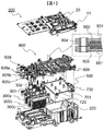
- FIG. FIG. 3 is an exploded perspective view disassembled into components for explaining the overall configuration of the bus bar assembly 800.
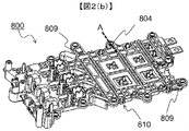
- 2 is an external perspective view of a bus bar assembly 800.
- FIG. 3 is a cross-sectional view of a bus bar assembly 800 when cut along a cross-section A in FIG. 2. It is sectional drawing of the bus-bar assembly 800 which concerns on another embodiment. It is sectional drawing of the bus-bar assembly 800 which concerns on another embodiment. It is sectional drawing of the bus-bar assembly 800 which concerns on another embodiment. It is sectional drawing of the bus-bar assembly 800 which concerns on another embodiment. It is sectional drawing of the bus-bar assembly 800 which concerns on another embodiment. It is sectional drawing of the bus-bar assembly 800 which concerns on another embodiment.
- the power conversion device 200 is mainly used for hybrid vehicles and electric vehicles.
- the power converter device 200 which concerns on this embodiment may be used for another use in order to achieve the effect.
- it may be used for a home appliance inverter of a refrigerator or an air conditioner for the purpose of improving productivity and cooling performance.
- the inverter may be used for an inverter for industrial equipment whose use environment is similar to that for a vehicle inverter.
- FIG. 1 is an exploded perspective view illustrating components of the power converter 200 according to the present embodiment in order to explain the overall configuration.
- the power converter 200 includes a circuit board 20, a metal base plate 11, a bus bar assembly 800, power semiconductor modules 300 a to 300 c, and a capacitor module 500. These members are housed in the case 220.
- Power semiconductor modules 300a to 300c described later convert DC power into AC power.
- the capacitor module 500 described later smoothes the DC power.
- the circuit board 20 described later is mounted with a drive circuit unit 20a (see FIG. 4) that outputs a drive signal for driving the power semiconductor modules 300a to 300c.
- the circuit board 20 includes a control circuit unit 20b (see FIG. 4) that outputs a control signal for controlling the power semiconductor modules 300a to 300c in the drive circuit.
- the case 220 forms a flow path forming body through which a coolant for cooling the power semiconductor modules 300a to 300b and the capacitor module 500 flows.
- the bus bar assembly 800 includes a DC side conductor plate 801, an insulating sheet 803, AC side conductor plates 805a to 805c, and an insulating member 802 for holding them, and further includes a current sensor 808.
- the DC side conductor plate 801 transmits DC power from the capacitor module 500 to the power semiconductor modules 300a to 300c.
- the DC side conductor plate 801 includes a positive electrode side conductor plate 801a and a negative electrode side conductor plate 801b.
- the electric power converted into AC by the power semiconductor modules 300a to 300c is output from the AC side conductor plates 805a to 805c.
- the AC side conductor plates 805a to 805c are disposed through the through holes of the current sensor 803.
- FIG. 2A is an exploded perspective view disassembled into components for explaining the overall configuration of the bus bar assembly 800.
- the bus bar assembly 800 is roughly composed of a first bus bar assembly 800a, a second bus bar assembly 800b, and an insulating sheet 803.
- the first bus bar assembly 800a faces the second bus bar assembly 800b with the insulating sheet 803 interposed therebetween.
- the first bus bar assembly 800a includes a positive-side conductor plate 801a and a first insulating member 802a having electrical insulation.
- the positive-side conductor plate 801a is covered with a first insulating member 802a in a state where one surface on the side facing the second bus bar assembly 800b is exposed.
- the second bus bar assembly 800b includes a negative-side conductor plate 801b and a second insulating member 802b having electrical insulation.
- the negative electrode side conductor plate 801b is covered with a second insulating member 802b in a state where one surface on the side facing the first bus bar assembly 800a is exposed.
- the insulating sheet 803 is disposed between the first bus bar assembly 800a and the second bus bar assembly 800b.
- the insulating sheet 803 is disposed so as to cover the exposed surfaces of the positive electrode side conductor plate 801a and the negative electrode side conductor plate 801b.
- the second insulating member 802b is formed to extend from a region facing the first bus bar assembly 800a so that the current sensor 808 is installed.
- connection terminals (described later) for connecting to the power semiconductor modules 300a to 300c are formed.
- connection terminals (described later) for connecting to the power semiconductor modules 300a to 300c are formed.
- through holes for inserting the terminals of the power semiconductor modules 300a to 300c are formed adjacent to the connection terminals.
- FIG. 2 (b) is an external perspective view of the bus bar assembly 800 in a state in which the components of the bus bar assembly 800 shown in FIG. 2 (a) are assembled. However, the AC side conductor plate 805 and the current sensor 808 are not shown.
- the bus bar assembly 800 is formed with two positioning through holes 809 that fit into the positioning pins 730 provided in the capacitor module 500.
- the first bus bar assembly 800a is locked to the second bus bar assembly 800b by the claw-shaped structural member fixing portion 810 with the insulating sheet 803 interposed therebetween.
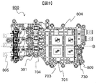
- FIG. 3 is a top view of the power conversion device 200 with the circuit board 20 and the board base plate 11 removed.
- the bus bar assembly 800 includes a capacitor connection portion 703 and a power module connection portion 704.
- the capacitor connection portion 703 and the power module connection portion 704 are connected to the DC side conductor plate 801 of the bus bar assembly 800.
- Capacitor connection portion 703 is connected to lead terminal 701 of capacitor 500.
- the power module connection unit 704 is connected to the DC terminal 301 of the power semiconductor module 300.
- the capacitor connection portion 703 and the power module connection portion 704 are formed to protrude in the same direction.
- the DC side conductor plate 801 of the bus bar assembly 800 is disposed above the capacitor module 500. As shown in FIG. 3, the DC side conductor plate 801 and the capacitor module 500 are joined to the lead terminal 701 extending upward from the capacitor module 500 by welding or the like, with the capacitor connecting portion 703 formed on the DC side conductor plate 801. With that, it is connected.
- a control circuit unit 20b of the circuit board 20 is disposed further above the capacitor module 500 with the bus bar assembly 800 interposed therebetween.
- a metal base plate 11 is disposed between the bus bar assembly 800 and the control circuit unit 20b.
- the control circuit unit 20b is more susceptible to noise than the drive circuit unit 20a because the voltage used is smaller than that of the drive circuit unit 20a. By disposing the metal base plate 11 between the bus bar assembly 800 and the control circuit unit 20b, it is possible to reduce the influence of noise propagating to the control circuit unit 20b.
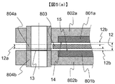
- FIG. 5A is a schematic view showing a cross section of the bus bar assembly 800 when cut along a cross section A in FIG.
- a convex structural member 804a is formed on the first insulating member 802a that holds the positive-side conductor plate 801a.
- the structural member 804a protrudes from one surface of the first insulating member 802a facing the second insulating member 802b toward the second insulating member 802b.
- the structural member 804a has a contact surface 13 in contact with the second insulating member 802b at the tip of the structural member 804a.
- the structural member 804a is formed so as to protrude from the exposed surface 14 in the normal direction of the exposed surface 14 of the positive-side conductor plate 801a.
- a through-hole penetrating in the protruding axis direction is formed in the convex structural member 804b.
- a fixing member such as a screw is inserted into the through hole.
- a plurality of structural members 804a are formed around the DC side conductor plate 801.
- the distance between the positive-side conductor plate 801a and the negative-electrode conductor plate 801b is controlled by the structural member 804a. Can do.
- the distance between the positive electrode side conductor plate 801a and the negative electrode side conductor plate 801b be as small as possible in order to obtain an inductance canceling effect more efficiently.
- the resin material decreases as the distance between the positive electrode and the negative electrode decreases.
- defects such as through holes are likely to occur.
- a short circuit occurs between the positive and negative electrodes, and it has been difficult in the past to achieve both electrical insulation and reduced inductance.
- an insulating sheet 803 different from the first insulating member 802a and the second insulating member 802b is disposed between the positive conductor plate 801a and the negative conductor plate 801b.
- the insulating sheet 803 for example, a laminate of PET materials or the like is used. These insulating materials are generally easy to process into a thin sheet. Further, since the insulating sheet 803 has a laminated structure, the through hole generated in each sheet is unlikely to be connected, and the insulation reliability is high.
- the distance 12 between the positive electrode side conductor plate 801a and the negative electrode side conductor plate 801b is equal to the thickness 12a of the insulating sheet 803.
- the sum of the necessary clearance 12b in consideration of the geometrical tolerance of the positive electrode side conductor plate 801a and the negative electrode side conductor plate 801b must be ensured at the minimum in production.
- the bus bar assembly 800 of the present embodiment can control the distance 12 between the positive-side conductor plate 801a and the negative-side conductor plate 801b to the minimum distance in manufacturing by the structural member 804a protruding from the first insulating member 801a. Therefore, an increase in inductance can be suppressed.
- the power conversion device includes the first insulating member 802a and the second insulating member 802b in the bus bar assembly 800 including the DC bus bar 801 that supplies a DC current to the power semiconductor module 300.
- Different insulating sheets 803 are sandwiched, and the first insulating member 802a has a convex structural member 804a protruding toward the second insulating member 802b. Therefore, the inductance from the DC power source to the power semiconductor module can be kept low, and electrical insulation can be ensured with high reliability.
- first insulating member 802a and the second insulating member constituting the bus bar assembly 800 are formed of an insulating resin member.
- the bus bar assembly 800 is formed, for example, by insert molding or the like in a state where the positive electrode side conductor plate 801a and the negative electrode side conductor plate 801b are exposed.
- the structural member 804a provided for securing the distance between the positive electrode side conductor plate 801a and the negative electrode side conductor plate 801b may be integrally formed of a resin material of the same material as the first insulating member 802a. In the example, it is formed of a metal member.
- the second insulating member 802b has a metal contact member 804b at a portion in contact with the metal structural member 804a of the first insulating member 802a.
- the contact member 804b forms the contact surface 13 between the contact member 804b and the convex shape 804a.
- the abutment surface 13 With metal materials, it is possible to make it difficult to cause shrinkage due to loads such as vibration and temperature.
- the contact surface 13 is formed of resin materials, there is a possibility that the resin material may be contracted on the contact surface 13, and it is difficult to maintain a reliable distance between the positive and negative conductor plates. According to the bus bar assembly 800 of the present embodiment, the inductance can be reduced with high reliability.
- the insulating member 802 constituting the bus bar assembly 800 has a structure for fixing the drive circuit portion 20a of the circuit board 20. As shown in FIG. 4, the drive circuit unit 20 a is disposed above the power semiconductor element 300. Since the drive circuit unit 20a uses a larger voltage than the control circuit unit 20b, the drive circuit unit 20a needs to have a sufficient insulation distance from other components compared to the control circuit unit 20b. Since the insulating member 802 is formed of an insulating resin material, it is not necessary to provide another insulating member between the driving circuit portion 20a and high-density mounting is possible.
- the conductor plate is generally made of copper with good electrical conductivity, and the thickness and width are determined by the current density.
- the distance between the conductor plates is preferably as close as possible for the purpose of reducing inductance.
- the distance between the conductor plate 801 and the metal boss 804a needs to be separated to a distance that allows insulation.
- the insulating sheet 803 is not the same size as the conductor plate 801, and needs to protrude to a certain distance from the edge of the conductor plate 801. .
- the insulating member 802 covering the DC side conductor plate 801 is fixed to the case 202 by, for example, bolt fastening. Accordingly, the weight of the DC side conductor plate 801 is applied to the case 220 via the insulating member 802. Thereby, concentration of stress applied to the contact portion between the lead terminal 703 and the DC side conductor plate 801 of the capacitor module 500 can be prevented. Therefore, for example, it is possible to incorporate a welded structure or the like into the joint, and it is possible to reduce the size and the number of parts.
- the current sensor 803 and the AC side conductor plate 805 are assembled to the insulating sheet 803 mounted on the bus bar assembly 800, and then the assembled bus bar assembly 800 is assembled.
- the power module 300 has a DC side terminal 301 and an AC side terminal 302, and the DC side terminal 301 and the AC side terminal are assembled by assembling the DC side conductor plate and the bus bar assembly 800 in which the AC side conductor plate is integrally assembled. Since the connection to 302 can be performed in the same assembly process, the assemblability can be improved.
- the power conversion device 200 is separated from the DC side conductor plate without integrating it with the capacitor module 500.
- the guaranteed temperature of the smoothing film capacitor cell 700 is lower than other components mounted on the power converter 200.
- the life of the film capacitor cell 700 is drastically reduced and the function as a smoothing capacitor is not satisfied. Therefore, by separating the DC side conductor plate from the capacitor module 500, it is possible to suppress the influence of tilting heat from the DC side conductor plate disposed on the upper part.
- Capacitor 500 has a case 720 for storing a capacitor cell, and case 720 is formed with positioning pins 730 that protrude in the direction in which bus bar assembly 800 is disposed, A positioning through hole 805 is formed in the insulating member 802 mounted on the bus bar assembly 800, and the positioning pin 730 is inserted into the positioning through hole 805.
- the capacitor connecting portion 703 formed on the DC side conductor plate 801 and the lead terminal 701 coming out of the capacitor can be arranged at the same position. Therefore, it is possible to improve the bonding reliability.
- the configuration of the power conversion device according to the second embodiment will be described.
- the part that is changed from the first embodiment is only the structure of the bus bar assembly 800, and therefore the description of the other configuration is omitted.
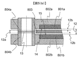
- FIG. 5B is a schematic diagram illustrating a cross section of the bus bar assembly 800 according to the second embodiment.
- a first structural member 804a protruding from the first insulating member 802a and a second structural member 804b protruding from the second insulating member 802b are formed.
- the first structural member 804a has a contact surface that contacts the front end of the second structural member 804b at the front end of the first structural member 804a.
- the first structural member 804a is formed so as to protrude from the exposed surface 14 in the normal direction of the exposed surface 14 of the positive-side conductor plate 801a.
- the second structural member 804b is formed so as to protrude from the exposed surface 15 in the normal direction of the exposed surface 15 of the negative-side conductor plate 801b.
- the first structural member 804a and the second structural member 804b are formed such that the sum of the protruding distance of the first structural member 804a and the protruding distance of the second structural member 804b is the conductor plate distance 12 shown in the first embodiment.
- the first insulating member 802a has a convex first structural member 804a and the second insulating member 802b has a convex second structural member 804b. Even if the relative position of the second structural member 804b is shifted due to vibration or the like, the second structural member 804b does not contact the first insulating member 802a or the second insulating member 802b. Therefore, the first insulating member 802a and the second insulating member 802b formed of a resin material can be prevented from being closed, and the distance between the conductor plates can be maintained with high reliability.
- through holes are provided in the first structural member 804a and the second structural member 804b. Since the through holes exist on the same axis, when the bus bar assembly 800 is mainly fixed with screws, the screws 800a and 800b can be fixed with screws through the respective through holes 804. Therefore, two different parts can be fixed at the same time, and the number of assembling steps can be reduced.
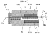
- FIG. 5C is a schematic diagram illustrating a cross section of the bus bar assembly 800 according to the third embodiment.
- the difference from the second embodiment is that a positioning hole 16 is formed in the insulating sheet 803, and the first structural member 804a or the second structural member 804b is formed so as to penetrate the positioning hole 16.
- the position is not defined in the exposed surface in-plane direction of the positive electrode side conductor plate 801a or the negative electrode side conductor plate 801b. If there is a region where the insulating sheet 803 is not formed between the exposed surface of the positive-side conductor plate 801a and the exposed surface of the negative-side conductor plate 801b, a necessary distance for ensuring insulation can be secured in that region. Therefore, there is a risk of impairing reliability.
- the bus bar assembly 800 of the present embodiment since the positioning hole 16 is formed in the insulating sheet 803, the position in the in-plane direction of the insulating sheet 803 is determined, so that the assembly workability is improved, the displacement with respect to vibration, etc. It becomes possible to suppress. Accordingly, it is possible to further improve the insulation between the positive and negative electrodes.
- 5 (d) and 5 (e) are diagrams showing another embodiment for securing a distance between the positive electrode side conductor plate 801a and the negative electrode side conductor plate 801b.
- the structural member for securing the distance between the pole-side conductor plate 801a and the negative-electrode side conductor plate 801b is a separate member from the first insulating member 802a and the second insulating member 802b.
- the bus bar assembly 800 shown in FIG. 5D has recesses formed in the first insulating member 802a and the second insulating member 802b made of insulating resin.
- the recesses are formed to face each other.
- a structural member 806 is inserted into the recess.
- the bus bar assembly 800 shown in FIG. 5 (e) has a T-shaped structural member 807.
- the T-shaped structural member 807 is an outer peripheral portion of the first insulating member 802a and the second insulating member 802b, and is disposed between the first insulating member 802a and the second insulating member 802b.
- the distance between the positive electrode side conductor plate 801a and the negative electrode side conductor plate 801b may be secured also by using a structure as shown in FIG. 5 (d) or FIG. 5 (e).
Landscapes
- Engineering & Computer Science (AREA)
- Power Engineering (AREA)
- Inverter Devices (AREA)
Abstract
Description
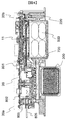
図4は、図3の断面Bで切断した断面図である。
バスバーアッセンブリ800に搭載される絶縁部材802に位置決め用貫通孔805が形成されており、位置決めピン730が位置決め用貫通孔805に挿通されるようになっている。
12:第1バスバーと第2バスバー間の距離
12a:絶縁物803の厚み
12b:第1バスバーと第2バスバー間の幾何公差を考慮した必要クリアランス
13:当接面
14:第1バスバーの第2バスバーと対向する面
15:第2バスバーの第1バスバーと対向する面
16:位置決め孔
20:回路基板
20a:駆動回路部
20b:制御回路部
200:電力変換装置、
220:ケース
300:パワー半導体モジュール
500:コンデンサモジュール
701:リード端子
703:コンデンサ接続部
704:パワーモジュール接続部
730:位置決めピン
800:バスバーアッセンブリ
801:直流側導体板
802:絶縁部材
803:絶縁シート
804:構造部材
805:交流側導体板
806:構造部材
807:T字型構造部材
808:電流センサ
809:位置決め用貫通孔
810:構造部材固定部
Claims (10)
- 直流電源からパワー半導体モジュールに直流電力を供給するバスバー構造であって、
前記バスバーは、第1バスバーと第2バスバーとを有し、
前記第1バスバーは、電気的に絶縁性を有する第1絶縁部材により、当該第1バスバーの一方の面が露出した状態で固定され、
前記第2バスバーは、電気的に絶縁性を有する第2絶縁部材により、当該第2バスバーの一方の面が露出した状態で固定され、
前記第1バスバーは、当該第1バスバーの前記一方の面が前記第2バスバーの前記一方の面と対向するように配置され、
前記第1バスバーと前記第2バスバーとの間には、前記第1及び第2絶縁部材とは異なる絶縁物が挟持され、
前記第1絶縁部材は、前記第2絶縁部材に向かって突出する第1突出部を有し、
前記第1突出部は、当該第1突出部の先端部に、前記第2絶縁部材に接する当接面を有するバスバー構造。 - 請求項1に記載されたバスバー構造であって、
前記第1絶縁部材及び前記第2絶縁部材は、樹脂により形成され、
前記第1突出部は、金属製の部材であり、
前記第2絶縁部材は、金属製の当接部材を有し、
前記当接部材は、前記第1突出部の先端部と接する前記当接面を有するバスバー構造。 - 請求項2に記載されたバスバー構造であって、
前記第2絶縁部材は、前記第1突出部に向かって突出する第2突出部を有し、
前記第2突出部は、当該第2突出部の先端部に、前記当接面を有するバスバー構造。 - 請求項1ないし3に記載されたいずれかのバスバー構造であって、
前記絶縁物には、位置決め孔が形成され、
前記絶縁物は、前記第1突出部が前記位置決め孔を貫通するように配置されるバスバー構造。 - 請求項1ないし4に記載されたいずれかのバスバー構造であって、
前記第1突出部は、当該第1突出部の軸方向に貫通する第1貫通孔が形成され、
前記第2絶縁部材は、前記第1貫通孔と同軸線上に第2貫通孔が形成され、
前記第1絶縁部材は、貫通部材を前記第1貫通孔と前記第2貫通孔に挿通することにより、前記第2絶縁部材に固定されるバスバー構造。 - 直流電源からパワー半導体モジュールに直流電力を供給するバスバー構造を備えた電力変換装置であって、
前記バスバーは、第1バスバーと第2バスバーとを有し、
前記第1バスバーは、電気的に絶縁性を有する第1絶縁部材により、当該第1バスバーの一方の面が露出した状態で固定され、
前記第2バスバーは、電気的に絶縁性を有する第2絶縁部材により、当該第2バスバーの一方の面が露出した状態で固定され、
前記第1バスバーは、当該第1バスバーの前記一方の面が前記第2バスバーの前記一方の面と対向するように配置され、
前記第1バスバーと前記第2バスバーとの間には、前記第1及び第2絶縁部材とは異なる絶縁物が挟持され、
前記第1絶縁部材は、前記第2絶縁部材に向かって突出する第1突出部を有し、
前記第1突出部は、当該第1突出部の先端部に、前記第2絶縁部材に接する当接面を有する電力変換装置。 - 請求項6に記載された電力変換装置であって、
前記第1絶縁部材及び前記第2絶縁部材は、樹脂により形成され、
前記第1突出部は、金属製の部材であり、
前記第2絶縁部材は、金属製の当接部材を有し、
前記当接部材は、前記第1突出部の先端部と接する前記当接面を有する電力変換装置。 - 請求項7に記載された電力変換装置であって、
前記第2絶縁部材は、前記第1突出部に向かって突出する第2突出部を有し、
前記第2突出部は、当該第2突出部の先端部に、前記当接面を有する電力変換装置。 - 請求項6ないし8に記載されたいずれかの電力変換装置であって、
前記絶縁物には、位置決め孔が形成され、
前記絶縁物は、前記第1突出部が前記位置決め孔を貫通するように配置される電力変換装置。 - 請求項6ないし9に記載されたいずれかの電力変換装置であって、
前記第1突出部は、当該第1突出部の軸方向に貫通する第1貫通孔が形成され、
前記第2絶縁部材は、前記第1貫通孔と同軸線上に第2貫通孔が形成され、
前記第1絶縁部材は、貫通部材を前記第1貫通孔と前記第2貫通孔に挿通することにより、前記第2絶縁部材に固定される電力変換装置。
Priority Applications (2)
| Application Number | Priority Date | Filing Date | Title |
|---|---|---|---|
| US15/030,109 US9667040B2 (en) | 2013-10-30 | 2014-09-24 | Bus bar structure and power converter using bus bar structure |
| JP2015544867A JP6222713B2 (ja) | 2013-10-30 | 2014-09-24 | バスバー構造及びバスバー構造を用いた電力変換装置 |
Applications Claiming Priority (2)
| Application Number | Priority Date | Filing Date | Title |
|---|---|---|---|
| JP2013-224879 | 2013-10-30 | ||
| JP2013224879 | 2013-10-30 |
Publications (1)
| Publication Number | Publication Date |
|---|---|
| WO2015064247A1 true WO2015064247A1 (ja) | 2015-05-07 |
Family
ID=53003860
Family Applications (1)
| Application Number | Title | Priority Date | Filing Date |
|---|---|---|---|
| PCT/JP2014/075151 Ceased WO2015064247A1 (ja) | 2013-10-30 | 2014-09-24 | バスバー構造及びバスバー構造を用いた電力変換装置 |
Country Status (3)
| Country | Link |
|---|---|
| US (1) | US9667040B2 (ja) |
| JP (1) | JP6222713B2 (ja) |
| WO (1) | WO2015064247A1 (ja) |
Cited By (4)
| Publication number | Priority date | Publication date | Assignee | Title |
|---|---|---|---|---|
| JP2017112168A (ja) * | 2015-12-15 | 2017-06-22 | パナソニックIpマネジメント株式会社 | フィルムコンデンサ |
| CN107924887A (zh) * | 2015-08-14 | 2018-04-17 | 施韦策电子公司 | 电子开关元件和模块化构造的变流器 |
| CN110178302A (zh) * | 2017-01-17 | 2019-08-27 | 日立汽车系统株式会社 | 电力转换装置 |
| JP7180812B1 (ja) | 2022-06-09 | 2022-11-30 | 富士電機株式会社 | 電力変換装置 |
Families Citing this family (10)
| Publication number | Priority date | Publication date | Assignee | Title |
|---|---|---|---|---|
| DE112015002670T5 (de) * | 2014-07-29 | 2017-02-23 | Hitachi Automotive Systems, Ltd. | Leistungsumsetzungsvorrichtung |
| JP6631463B2 (ja) * | 2016-10-17 | 2020-01-15 | 株式会社デンソー | 電力変換装置 |
| DE102018118525A1 (de) * | 2018-07-31 | 2020-02-06 | Valeo Siemens Eautomotive Germany Gmbh | Anordnung mit einer Stromschienenvorrichtung und einem Stromrichtergehäuse sowie Verfahren zu deren Herstellung, Stromrichter für ein Fahrzeug und Fahrzeug |
| EP3609066B1 (en) * | 2018-08-07 | 2021-02-24 | Mahle International GmbH | Electric power inverter |
| US12500398B2 (en) | 2018-10-31 | 2025-12-16 | Lear Corporation | Electrical assembly |
| US11721956B2 (en) | 2018-10-31 | 2023-08-08 | Lear Corporation | Electrical assembly |
| US11858437B2 (en) | 2018-10-31 | 2024-01-02 | Lear Corporation | Electrical assembly |
| US11735891B2 (en) | 2018-10-31 | 2023-08-22 | Lear Corporation | Electrical assembly |
| WO2020174641A1 (ja) | 2019-02-28 | 2020-09-03 | Tdk株式会社 | 直流給電システム |
| DE102023200221B4 (de) * | 2023-01-12 | 2025-03-27 | Zf Friedrichshafen Ag | Stromschiene zur Leitung von Strom für eine Leistungselektronik |
Citations (3)
| Publication number | Priority date | Publication date | Assignee | Title |
|---|---|---|---|---|
| JP2003009507A (ja) * | 2001-06-15 | 2003-01-10 | Toyota Motor Corp | スイッチング回路 |
| WO2011093239A1 (ja) * | 2010-01-27 | 2011-08-04 | 株式会社日立製作所 | 配電実装部品及びそれを用いたインバータ装置 |
| JP2012095472A (ja) * | 2010-10-28 | 2012-05-17 | Mitsubishi Electric Corp | 電力変換装置 |
Family Cites Families (10)
| Publication number | Priority date | Publication date | Assignee | Title |
|---|---|---|---|---|
| JP3550970B2 (ja) * | 1997-09-19 | 2004-08-04 | 株式会社日立製作所 | 電力変換装置並びに多層積層導体と電気部品接続体 |
| JP3793407B2 (ja) * | 2000-09-19 | 2006-07-05 | 株式会社日立製作所 | 電力変換装置 |
| JP2004304874A (ja) | 2003-03-28 | 2004-10-28 | Toyota Motor Corp | バスバーモジュール及びバスバーモジュール製造方法 |
| JP2010259139A (ja) * | 2009-04-21 | 2010-11-11 | Fuji Electric Systems Co Ltd | 絶縁ブスバー及びこれを使用した電力変換装置 |
| JP5450042B2 (ja) * | 2009-12-25 | 2014-03-26 | 日立オートモティブシステムズ株式会社 | アクチュエータの制御装置 |
| JP5549491B2 (ja) * | 2010-09-06 | 2014-07-16 | 日立金属株式会社 | バスバーモジュールの製造方法、及びバスバーモジュール |
| JP6458444B2 (ja) * | 2014-10-21 | 2019-01-30 | 株式会社デンソー | 電力変換装置 |
| US10199804B2 (en) * | 2014-12-01 | 2019-02-05 | Tesla, Inc. | Busbar locating component |
| US9536671B2 (en) * | 2014-12-01 | 2017-01-03 | Telsa Motors, Inc. | Planar capacitor terminals |
| US11218080B2 (en) * | 2015-08-31 | 2022-01-04 | Faraday & Future Inc. | Inverter AC bus bar assembly |
-
2014
- 2014-09-24 JP JP2015544867A patent/JP6222713B2/ja not_active Expired - Fee Related
- 2014-09-24 US US15/030,109 patent/US9667040B2/en active Active
- 2014-09-24 WO PCT/JP2014/075151 patent/WO2015064247A1/ja not_active Ceased
Patent Citations (3)
| Publication number | Priority date | Publication date | Assignee | Title |
|---|---|---|---|---|
| JP2003009507A (ja) * | 2001-06-15 | 2003-01-10 | Toyota Motor Corp | スイッチング回路 |
| WO2011093239A1 (ja) * | 2010-01-27 | 2011-08-04 | 株式会社日立製作所 | 配電実装部品及びそれを用いたインバータ装置 |
| JP2012095472A (ja) * | 2010-10-28 | 2012-05-17 | Mitsubishi Electric Corp | 電力変換装置 |
Cited By (7)
| Publication number | Priority date | Publication date | Assignee | Title |
|---|---|---|---|---|
| CN107924887A (zh) * | 2015-08-14 | 2018-04-17 | 施韦策电子公司 | 电子开关元件和模块化构造的变流器 |
| CN107924887B (zh) * | 2015-08-14 | 2022-01-25 | 施韦策电子公司 | 电子开关元件和模块化构造的变流器 |
| JP2017112168A (ja) * | 2015-12-15 | 2017-06-22 | パナソニックIpマネジメント株式会社 | フィルムコンデンサ |
| CN110178302A (zh) * | 2017-01-17 | 2019-08-27 | 日立汽车系统株式会社 | 电力转换装置 |
| CN110178302B (zh) * | 2017-01-17 | 2021-09-10 | 日立汽车系统株式会社 | 电力转换装置 |
| JP7180812B1 (ja) | 2022-06-09 | 2022-11-30 | 富士電機株式会社 | 電力変換装置 |
| JP2023180525A (ja) * | 2022-06-09 | 2023-12-21 | 富士電機株式会社 | 電力変換装置 |
Also Published As
| Publication number | Publication date |
|---|---|
| US20160268782A1 (en) | 2016-09-15 |
| US9667040B2 (en) | 2017-05-30 |
| JPWO2015064247A1 (ja) | 2017-03-09 |
| JP6222713B2 (ja) | 2017-11-01 |
Similar Documents
| Publication | Publication Date | Title |
|---|---|---|
| JP6222713B2 (ja) | バスバー構造及びバスバー構造を用いた電力変換装置 | |
| US10199804B2 (en) | Busbar locating component | |
| JP5799843B2 (ja) | 電力変換装置 | |
| CN110829861B (zh) | 电力转换器 | |
| US11296613B2 (en) | Power conversion device | |
| JP5374979B2 (ja) | 電池と組電池 | |
| JP6190213B2 (ja) | 電池パック | |
| US11770915B2 (en) | Electrical equipment comprising a busbar cooled by two faces of a heatsink | |
| US12341438B2 (en) | Power converter | |
| JP2006230064A (ja) | 電力変換ユニット | |
| US20240055781A1 (en) | Power electronic devices with busbars and method for their fabrication | |
| WO2019193903A1 (ja) | 電力変換装置及びコンデンサモジュール | |
| WO2015083476A1 (ja) | 電力変換装置 | |
| CN113678311B (zh) | 包括高压线组件的电池组和用于制造该电池组的方法 | |
| JP5817702B2 (ja) | 半導体モジュール | |
| JP2006196222A (ja) | 電池セル結合体、組電池構造およびその組み立て方法 | |
| JP7005732B1 (ja) | 電力変換装置及びその製造方法 | |
| JP6203232B2 (ja) | パワーモジュール | |
| JP6327770B2 (ja) | 電池パック | |
| US20240235410A9 (en) | Power Conversion Apparatus | |
| US20260074626A1 (en) | Power conversion device and capacitor device | |
| JP7019092B2 (ja) | 素子モジュール | |
| US20250048605A1 (en) | Semiconductor device and insulating member | |
| JP2015171309A (ja) | 回路構成体及び電気接続箱 |
Legal Events
| Date | Code | Title | Description |
|---|---|---|---|
| 121 | Ep: the epo has been informed by wipo that ep was designated in this application |
Ref document number: 14857116 Country of ref document: EP Kind code of ref document: A1 |
|
| WWE | Wipo information: entry into national phase |
Ref document number: 15030109 Country of ref document: US |
|
| ENP | Entry into the national phase |
Ref document number: 2015544867 Country of ref document: JP Kind code of ref document: A |
|
| NENP | Non-entry into the national phase |
Ref country code: DE |
|
| 122 | Ep: pct application non-entry in european phase |
Ref document number: 14857116 Country of ref document: EP Kind code of ref document: A1 |