WO2015064231A1 - 半導体モジュール - Google Patents
半導体モジュール Download PDFInfo
- Publication number
- WO2015064231A1 WO2015064231A1 PCT/JP2014/074484 JP2014074484W WO2015064231A1 WO 2015064231 A1 WO2015064231 A1 WO 2015064231A1 JP 2014074484 W JP2014074484 W JP 2014074484W WO 2015064231 A1 WO2015064231 A1 WO 2015064231A1
- Authority
- WO
- WIPO (PCT)
- Prior art keywords
- metal foil
- solder
- semiconductor element
- pin
- semiconductor module
- Prior art date
- Legal status (The legal status is an assumption and is not a legal conclusion. Google has not performed a legal analysis and makes no representation as to the accuracy of the status listed.)
- Ceased
Links
Images



Classifications
-
- H—ELECTRICITY
- H10—SEMICONDUCTOR DEVICES; ELECTRIC SOLID-STATE DEVICES NOT OTHERWISE PROVIDED FOR
- H10W—GENERIC PACKAGES, INTERCONNECTIONS, CONNECTORS OR OTHER CONSTRUCTIONAL DETAILS OF DEVICES COVERED BY CLASS H10
- H10W40/00—Arrangements for thermal protection or thermal control
- H10W40/20—Arrangements for cooling
- H10W40/25—Arrangements for cooling characterised by their materials
- H10W40/255—Arrangements for cooling characterised by their materials having a laminate or multilayered structure, e.g. direct bond copper [DBC] ceramic substrates
-
- H—ELECTRICITY
- H10—SEMICONDUCTOR DEVICES; ELECTRIC SOLID-STATE DEVICES NOT OTHERWISE PROVIDED FOR
- H10W—GENERIC PACKAGES, INTERCONNECTIONS, CONNECTORS OR OTHER CONSTRUCTIONAL DETAILS OF DEVICES COVERED BY CLASS H10
- H10W70/00—Package substrates; Interposers; Redistribution layers [RDL]
- H10W70/60—Insulating or insulated package substrates; Interposers; Redistribution layers
- H10W70/62—Insulating or insulated package substrates; Interposers; Redistribution layers characterised by their interconnections
- H10W70/65—Shapes or dispositions of interconnections
-
- H—ELECTRICITY
- H10—SEMICONDUCTOR DEVICES; ELECTRIC SOLID-STATE DEVICES NOT OTHERWISE PROVIDED FOR
- H10W—GENERIC PACKAGES, INTERCONNECTIONS, CONNECTORS OR OTHER CONSTRUCTIONAL DETAILS OF DEVICES COVERED BY CLASS H10
- H10W72/00—Interconnections or connectors in packages
-
- H—ELECTRICITY
- H10—SEMICONDUCTOR DEVICES; ELECTRIC SOLID-STATE DEVICES NOT OTHERWISE PROVIDED FOR
- H10W—GENERIC PACKAGES, INTERCONNECTIONS, CONNECTORS OR OTHER CONSTRUCTIONAL DETAILS OF DEVICES COVERED BY CLASS H10
- H10W90/00—Package configurations
-
- H—ELECTRICITY
- H10—SEMICONDUCTOR DEVICES; ELECTRIC SOLID-STATE DEVICES NOT OTHERWISE PROVIDED FOR
- H10W—GENERIC PACKAGES, INTERCONNECTIONS, CONNECTORS OR OTHER CONSTRUCTIONAL DETAILS OF DEVICES COVERED BY CLASS H10
- H10W90/00—Package configurations
- H10W90/401—Package configurations characterised by multiple insulating or insulated package substrates, interposers or RDLs
-
- H—ELECTRICITY
- H10—SEMICONDUCTOR DEVICES; ELECTRIC SOLID-STATE DEVICES NOT OTHERWISE PROVIDED FOR
- H10W—GENERIC PACKAGES, INTERCONNECTIONS, CONNECTORS OR OTHER CONSTRUCTIONAL DETAILS OF DEVICES COVERED BY CLASS H10
- H10W90/00—Package configurations
- H10W90/701—Package configurations characterised by the relative positions of pads or connectors relative to package parts
-
- H—ELECTRICITY
- H10—SEMICONDUCTOR DEVICES; ELECTRIC SOLID-STATE DEVICES NOT OTHERWISE PROVIDED FOR
- H10W—GENERIC PACKAGES, INTERCONNECTIONS, CONNECTORS OR OTHER CONSTRUCTIONAL DETAILS OF DEVICES COVERED BY CLASS H10
- H10W40/00—Arrangements for thermal protection or thermal control
- H10W40/20—Arrangements for cooling
- H10W40/22—Arrangements for cooling characterised by their shape, e.g. having conical or cylindrical projections
-
- H—ELECTRICITY
- H10—SEMICONDUCTOR DEVICES; ELECTRIC SOLID-STATE DEVICES NOT OTHERWISE PROVIDED FOR
- H10W—GENERIC PACKAGES, INTERCONNECTIONS, CONNECTORS OR OTHER CONSTRUCTIONAL DETAILS OF DEVICES COVERED BY CLASS H10
- H10W40/00—Arrangements for thermal protection or thermal control
- H10W40/40—Arrangements for thermal protection or thermal control involving heat exchange by flowing fluids
- H10W40/47—Arrangements for thermal protection or thermal control involving heat exchange by flowing fluids by flowing liquids, e.g. forced water cooling
-
- H—ELECTRICITY
- H10—SEMICONDUCTOR DEVICES; ELECTRIC SOLID-STATE DEVICES NOT OTHERWISE PROVIDED FOR
- H10W—GENERIC PACKAGES, INTERCONNECTIONS, CONNECTORS OR OTHER CONSTRUCTIONAL DETAILS OF DEVICES COVERED BY CLASS H10
- H10W40/00—Arrangements for thermal protection or thermal control
- H10W40/70—Fillings or auxiliary members in containers or in encapsulations for thermal protection or control
- H10W40/73—Fillings or auxiliary members in containers or in encapsulations for thermal protection or control for cooling by change of state
-
- H—ELECTRICITY
- H10—SEMICONDUCTOR DEVICES; ELECTRIC SOLID-STATE DEVICES NOT OTHERWISE PROVIDED FOR
- H10W—GENERIC PACKAGES, INTERCONNECTIONS, CONNECTORS OR OTHER CONSTRUCTIONAL DETAILS OF DEVICES COVERED BY CLASS H10
- H10W40/00—Arrangements for thermal protection or thermal control
- H10W40/70—Fillings or auxiliary members in containers or in encapsulations for thermal protection or control
- H10W40/77—Auxiliary members characterised by their shape
- H10W40/778—Auxiliary members characterised by their shape in encapsulations
-
- H—ELECTRICITY
- H10—SEMICONDUCTOR DEVICES; ELECTRIC SOLID-STATE DEVICES NOT OTHERWISE PROVIDED FOR
- H10W—GENERIC PACKAGES, INTERCONNECTIONS, CONNECTORS OR OTHER CONSTRUCTIONAL DETAILS OF DEVICES COVERED BY CLASS H10
- H10W72/00—Interconnections or connectors in packages
- H10W72/071—Connecting or disconnecting
- H10W72/073—Connecting or disconnecting of die-attach connectors
- H10W72/07351—Connecting or disconnecting of die-attach connectors characterised by changes in properties of the die-attach connectors during connecting
- H10W72/07354—Connecting or disconnecting of die-attach connectors characterised by changes in properties of the die-attach connectors during connecting changes in dispositions
-
- H—ELECTRICITY
- H10—SEMICONDUCTOR DEVICES; ELECTRIC SOLID-STATE DEVICES NOT OTHERWISE PROVIDED FOR
- H10W—GENERIC PACKAGES, INTERCONNECTIONS, CONNECTORS OR OTHER CONSTRUCTIONAL DETAILS OF DEVICES COVERED BY CLASS H10
- H10W72/00—Interconnections or connectors in packages
- H10W72/30—Die-attach connectors
- H10W72/341—Dispositions of die-attach connectors, e.g. layouts
- H10W72/347—Dispositions of multiple die-attach connectors
-
- H—ELECTRICITY
- H10—SEMICONDUCTOR DEVICES; ELECTRIC SOLID-STATE DEVICES NOT OTHERWISE PROVIDED FOR
- H10W—GENERIC PACKAGES, INTERCONNECTIONS, CONNECTORS OR OTHER CONSTRUCTIONAL DETAILS OF DEVICES COVERED BY CLASS H10
- H10W72/00—Interconnections or connectors in packages
- H10W72/30—Die-attach connectors
- H10W72/351—Materials of die-attach connectors
- H10W72/352—Materials of die-attach connectors comprising metals or metalloids, e.g. solders
-
- H—ELECTRICITY
- H10—SEMICONDUCTOR DEVICES; ELECTRIC SOLID-STATE DEVICES NOT OTHERWISE PROVIDED FOR
- H10W—GENERIC PACKAGES, INTERCONNECTIONS, CONNECTORS OR OTHER CONSTRUCTIONAL DETAILS OF DEVICES COVERED BY CLASS H10
- H10W74/00—Encapsulations, e.g. protective coatings
-
- H—ELECTRICITY
- H10—SEMICONDUCTOR DEVICES; ELECTRIC SOLID-STATE DEVICES NOT OTHERWISE PROVIDED FOR
- H10W—GENERIC PACKAGES, INTERCONNECTIONS, CONNECTORS OR OTHER CONSTRUCTIONAL DETAILS OF DEVICES COVERED BY CLASS H10
- H10W74/00—Encapsulations, e.g. protective coatings
- H10W74/10—Encapsulations, e.g. protective coatings characterised by their shape or disposition
- H10W74/111—Encapsulations, e.g. protective coatings characterised by their shape or disposition the semiconductor body being completely enclosed
- H10W74/114—Encapsulations, e.g. protective coatings characterised by their shape or disposition the semiconductor body being completely enclosed by a substrate and the encapsulations
-
- H—ELECTRICITY
- H10—SEMICONDUCTOR DEVICES; ELECTRIC SOLID-STATE DEVICES NOT OTHERWISE PROVIDED FOR
- H10W—GENERIC PACKAGES, INTERCONNECTIONS, CONNECTORS OR OTHER CONSTRUCTIONAL DETAILS OF DEVICES COVERED BY CLASS H10
- H10W90/00—Package configurations
- H10W90/701—Package configurations characterised by the relative positions of pads or connectors relative to package parts
- H10W90/731—Package configurations characterised by the relative positions of pads or connectors relative to package parts of die-attach connectors
- H10W90/734—Package configurations characterised by the relative positions of pads or connectors relative to package parts of die-attach connectors between a chip and a stacked insulating package substrate, interposer or RDL
Definitions
- the present invention relates to a semiconductor module that can improve cooling capacity in a semiconductor module using pin bonding.
- Patent Documents 1 and 2 are known as documents disclosing semiconductor modules using pin bonding.
- FIG. 1 of Patent Document 1 discloses a structure in which an implant pin pierced on a printed board and a semiconductor element are electrically joined.
- Patent Document 2 discloses that a semiconductor element and a plurality of post electrodes are joined by solder.
- Patent Documents 1 and 2 are documents that disclose a semiconductor module having a pin junction structure, which has been conceived as a measure for suppressing a peeling phenomenon between a wire frame and an electrode due to long-term use. However, since the cooling is performed from only one side of the semiconductor element, the cooling capacity is low, and it is difficult to fully exhibit the capacity of the semiconductor element.
- an object of the present invention is to provide a semiconductor module capable of improving the cooling capacity in a semiconductor module using pin bonding.
- the inventors have found that in a semiconductor module using pin bonding, the cooling capacity of the semiconductor module can be improved by optimizing the thickness of the solder for bonding the pin and the semiconductor element, and the present invention has been achieved.
- a semiconductor module of the present invention includes a semiconductor element, pins electrically and thermally connected to one surface of the semiconductor element, an insulating substrate for pin wiring, and an insulating substrate for pin wiring.
- Pin wiring board solder that joins the pin and the semiconductor element, a ceramic insulating substrate, a third metal foil disposed on the upper surface of the ceramic insulating substrate, and a fourth metal disposed on the lower surface of the ceramic insulating substrate
- a semiconductor module comprising a DCB substrate having a foil, the third metal foil being bonded to the lower surface of the semiconductor element, and a first cooler thermally connected to the fourth metal foil.
- H / T which is a ratio of the height H of the solder and the distance T from the semiconductor element to the first metal foil of the insulating substrate for pin wiring, is 0.2 or more; 7 or less.
- the solder linear expansion coefficient is preferably less than 22.0 ppm / K.
- the solder is preferably SnSb solder.
- the SnSb solder preferably contains 13% by mass of Sb as a main component.
- solder can be used as the solder.
- the heat generated in the semiconductor element is transferred to both the pin wiring board that is pin-bonded to the surface of the semiconductor element by soldering and the ceramic insulating substrate that is solder-bonded to the back surface of the semiconductor element.
- the ratio (H / T) between the solder height H and the distance T from the semiconductor element to the first metal foil is 0.2 or more and 0.7 or less. The effect can alleviate the transient phenomenon of heat transfer and suppress the temperature rise on the surface of the semiconductor element.
- FIG. 1 is a schematic cross-sectional view of a semiconductor module 100 according to the present invention.
- the semiconductor module 100 includes a semiconductor element 1, a DCB substrate 2, a ceramic insulating substrate 2a, a third metal foil 2b, a fourth metal foil 2c, a solder 3a, a solder 3b, a solder 3c, a pin 4, a pin wiring substrate 5, and a pin wiring.
- Insulating substrate 5a, first metal foil (circuit layer) 5b, second metal foil 5c, first cooler 6, first refrigerant passage 6a, fin 6b, external terminal 7a, external terminal 7b, and sealing resin 8 are provided.
- the semiconductor element 1 is not particularly limited, but, for example, an IGBT (Insulated Gate Bipolar Transistor), a power MOSFET (Metal Oxide Semiconductor Field Transistor Transistor), or an FWD (Free Wheeling1) element, which may be one of the two semiconductor elements.
- IGBT Insulated Gate Bipolar Transistor
- MOSFET Metal Oxide Semiconductor Field Transistor Transistor
- FWD Free Wheeling1
- RB-IGBT Reverse Blocking-Insulated Gate Bipolar Transistor
- RC-IGBT Reverse Conducting-Insulated Gate Bipolar Transistor
- the pin wiring substrate 5 includes a pin wiring insulating substrate 5a, a first metal foil (circuit layer) 5b, and a second metal foil 5c, and is arranged so that the first metal foil (circuit layer) 5b faces the semiconductor element 1.
- the pin wiring insulating substrate 5a is not particularly limited, but a material having a low dielectric constant and high thermal conductivity is preferable.
- a polyimide resin or a glass epoxy resin can be used.
- the pin wiring board 5 is not necessarily a printed board, and may be a copper thin plate, for example.
- the first metal foil (circuit layer) 5b and the second metal foil 5c are not particularly limited, but are preferably made of a material having low electrical resistance and high thermal conductivity. For example, copper can be used.
- the pin 4 is not particularly limited, but is preferably a metal with low electrical resistance and high thermal conductivity, specifically copper.
- One end of the pin 4 is soldered to the upper surface of the semiconductor element 1 by the solder 3c, and the other end penetrates the pin wiring board 5 and is joined to the first metal foil (circuit layer) 5b and the second metal foil 5c. .
- the pin 4 can be firmly fixed to the semiconductor element 1 and the pin wiring substrate 5, and the heat generated in the semiconductor element 1 can be transferred to the second metal foil 5 c via the pin 4.
- the cooling efficiency of the module 100 can be increased.
- the first cooler 6 is hollow inside and includes a plurality of fins 6b. A space between the fins 6b is a refrigerant passage 6a.
- the refrigerant is not particularly limited.
- a liquid refrigerant such as an ethylene glycol aqueous solution or water can be used, a gas refrigerant such as air can be used, or the refrigerant can be evaporated by a cooler such as Freon.
- a phase-changeable refrigerant that cools the cooler with heat of vaporization can also be used.
- the DCB substrate 2 includes a ceramic insulating substrate 2a, a third metal foil 2b, and a fourth metal foil 2c.
- the third metal foil 2b is disposed on the upper surface of the ceramic insulating substrate 2a, and the fourth metal is disposed on the lower surface of the ceramic insulating substrate 2a.
- a foil 2c is arranged.
- the third metal foil 2 b of the DCB substrate 2 is bonded to the lower surface of the semiconductor element 1.
- DCB is an abbreviation for Direct Copper Bonding, and a metal foil such as copper is directly bonded to a ceramic insulating substrate. Since the ceramic insulating substrate 2a is insulative, the third metal foil 2b and the fourth metal foil 2c are electrically insulated.
- the material of the ceramic insulating substrate 2a is not particularly limited, but is preferably a material having high thermal conductivity. For example, Si 3 N 4 , AlN, or Al 2 O 3 can be used.
- the solder 3a is electrically and thermally connected by connecting the lower surface of the semiconductor element 1 and the third metal foil 2b.
- the solder 3 b connects the fourth metal foil 2 c of the DCB substrate 2 and the outer wall of the first cooler 6, and transfers heat transferred from the semiconductor element 1 to the DCB substrate 2 to the first cooler 6. .
- External terminals 7a and 7b are terminals for conducting between the semiconductor element 1 and the outside, and the main power is conducted.
- the external terminals 7a and 7b are electrically connected to the third metal foil 2b of the DCB substrate 2 by solder and are led out from the upper surface.
- the semiconductor module 100 includes a control terminal (not shown).
- the control terminal is a terminal for controlling the semiconductor element 1, and the semiconductor element 1 is controlled from the outside.
- the sealing resin 8 is illustrated in a bonding surface between the first cooler 6 of the semiconductor module 100 and the fourth metal foil 2c of the first cooler 6, and a region led out of the external terminals 7a and 7b. It is sealed with a sealing resin except for a region led to the outside of the control terminals that are not.
- the sealing resin 8 is not particularly limited as long as it has a predetermined insulating performance and good moldability. For example, an epoxy resin is preferably used.
- the semiconductor module shown in FIG. 1 has only one semiconductor element, but may have a structure including a plurality of pairs of semiconductor elements 1 and pins 4.
- the rated output that can be processed by the semiconductor module can be increased.
- the types of the plurality of semiconductor elements 1 may be changed to different types of semiconductor elements. For example, an IGBT and FWD may be connected in parallel.
- the pin 4 is soldered to the upper surface of the semiconductor element 1 by solder 3c.
- a gap is provided between the surface of the solder 3 c and the first metal foil (circuit layer) 5 b of the pin wiring substrate 5.
- the height of the solder is H
- the distance from the semiconductor element to the first metal foil of the insulating substrate for pin wiring is T.
- the solder may go up around the pin.
- the solder height H is the height from the interface between the semiconductor element and the solder to the lowermost surface of the upper surface of the solder.
- the solder height H is the height from the interface between the semiconductor element and the solder to the lowermost surface of the upper surface of the solder between the pins.
- the ratio H / T between the height H of the solder and the distance T from the semiconductor element to the first metal foil of the insulating substrate for pin wiring is 0.2 or more, 0 .7 or less is preferable. If H / T is less than 0.2, the heat storage effect of the solder in the transient heat state is not sufficient, and the semiconductor element maximum temperature Tj exceeds the safe temperature range. If it is higher than 0.7, the stress applied to the semiconductor element becomes too large, and some of them break in high temperature operation tests and thermal cycle tests.
- H / T which is a ratio between the solder height H and the distance T from the semiconductor element to the first metal foil of the insulating substrate for pin wiring, is 0.2 or more, Since it is in the range of 0.7 or less, the semiconductor element maximum temperature Tj in the transient heat state can be reduced by the heat storage effect of the solder, and the stress to the semiconductor element can be reduced.
- the H / T is more preferably in the range of 0.26 or more and 0.53 or less. According to such a configuration, the cooling capacity of the semiconductor module can be further improved, the stress applied to the semiconductor element can be reduced, and the life of the semiconductor module can be improved.
- the solder has a linear expansion coefficient of less than 22.0 ppm / K. Furthermore, it is more preferable that the linear expansion coefficient of the solder is 21.2 ppm / K or less.
- the linear expansion coefficient of the solder is 22.0 ppm / K or more, when the semiconductor element generates heat, thermal stress is generated due to the difference in linear expansion coefficient between the pin and the solder, and the thermal stress is easily applied to the semiconductor element.
- the linear expansion coefficient of the solder can be brought close to the linear expansion coefficient of the pin, and the thermal stress applied to the semiconductor element can be reduced.
- the material of the pin is not particularly limited as long as it has a high thermal conductivity and is closer to the linear expansion coefficient of the solder, but it is desirable to use copper having a high thermal conductivity.
- SnSb solder or SnAg solder can be preferably used as the solder.
- the main component of SnSb solder is desirably Sn13Sb. Since Sn13Sb solder has a linear expansion coefficient of 21.2 ppm / K or less, it can reduce the thermal stress applied to the semiconductor element.
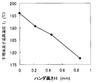
- FIG. 2 shows the relationship between the solder height H and the semiconductor element maximum temperature Tj. It can be seen that the higher the solder height H, the lower the semiconductor element maximum temperature Tj during the operation of the semiconductor element 1.
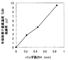
- FIG. 3 is a graph showing the relationship between the solder height and the reduction rate of the semiconductor element maximum temperature Tj obtained by conversion from FIG. It can be seen that increasing the solder height H has a temperature reduction effect of a little over 9%.
- FIG. 4 is a diagram showing the relationship between the solder height H and the stress applied to the semiconductor element 1. It can be seen that when the solder height H is increased, the chip stress increases and exceeds 240 MPa.
- FIG. 5 is a diagram showing the relationship between the solder height ratio H / T and the reduction rate of the semiconductor element maximum temperature Tj
- FIG. 6 shows the solder height ratio H / T and the reduction rate of the stress applied to the semiconductor element 1. It is a figure which shows a relationship.
- the solder height ratio H / T is 0.2 or more
- the semiconductor element maximum temperature Tj can be reduced by 2% or more
- the safe temperature range can be expanded by 4 ° C.
- the solder height ratio H / T is 0.7 or less, the stress can be reduced by 6% or more, and the failure rate is improved in the high temperature operation test.
Landscapes
- Cooling Or The Like Of Semiconductors Or Solid State Devices (AREA)
- Chemical & Material Sciences (AREA)
- Engineering & Computer Science (AREA)
- Ceramic Engineering (AREA)
- Physics & Mathematics (AREA)
- Geometry (AREA)
Abstract
Description
2 DCB基板
2a セラミック絶縁基板
2b 第3金属箔
2c 第4金属箔
3a,3b,3c ハンダ
4 ピン
5 ピン配線基板
5a ピン配線用絶縁基板
5b 第1金属箔(回路層)
5c 第2金属箔
6 第1冷却器
6a 第1冷媒通路
6b フィン
7a,7b 外部端子
8 封止樹脂
100 半導体モジュール
Claims (5)
- 半導体素子と、
前記半導体素子の一方の面に電気的および熱的に接続されたピンと、
ピン配線用絶縁基板、前記ピン配線用絶縁基板の下面に配置した第1金属箔、および前記ピン配線用絶縁基板の上面に配置した第2金属箔を備えており、かつ前記第1金属箔と前記第2金属箔と前記ピンとが電気的に接合しているピン配線基板と、
前記ピンと前記半導体素子を接合したハンダと、
セラミック絶縁基板、前記セラミック絶縁基板の上面に配置した第3金属箔、および前記セラミック絶縁基板の下面に配置した第4金属箔を備えており、前記第3金属箔が前記半導体素子の下面に接合されているDCB基板と、
前記第4金属箔に熱的に接続された第1冷却器と、
を備えた半導体モジュールであって、
前記ハンダの高さHと、前記半導体素子から前記ピン配線用絶縁基板の前記第1金属箔までの間の距離Tとの比であるH/Tが0.2以上、0.7以下の範囲内であることを特徴とする半導体モジュール。 - 前記ハンダの線膨張係数が22.0ppm/K未満である請求項1に記載の半導体モジュール。
- 前記ハンダは、SnSb系ハンダである請求項1又は2に記載の半導体モジュール。
- 前記SnSb系ハンダは、主成分としてSbを13質量%含有する請求項3に記載の半導体モジュール。
- 前記ハンダは、SnAg系ハンダである請求項1又は2に記載の半導体モジュール。
Priority Applications (4)
| Application Number | Priority Date | Filing Date | Title |
|---|---|---|---|
| CN201480020473.6A CN105103286B (zh) | 2013-10-30 | 2014-09-17 | 半导体模块 |
| DE112014001491.5T DE112014001491T5 (de) | 2013-10-30 | 2014-09-17 | Halbleitermodul |
| JP2015544858A JP6149938B2 (ja) | 2013-10-30 | 2014-09-17 | 半導体モジュール |
| US14/878,596 US9299637B2 (en) | 2013-10-30 | 2015-10-08 | Semiconductor module |
Applications Claiming Priority (2)
| Application Number | Priority Date | Filing Date | Title |
|---|---|---|---|
| JP2013-225513 | 2013-10-30 | ||
| JP2013225513 | 2013-10-30 |
Related Child Applications (1)
| Application Number | Title | Priority Date | Filing Date |
|---|---|---|---|
| US14/878,596 Continuation US9299637B2 (en) | 2013-10-30 | 2015-10-08 | Semiconductor module |
Publications (1)
| Publication Number | Publication Date |
|---|---|
| WO2015064231A1 true WO2015064231A1 (ja) | 2015-05-07 |
Family
ID=53003844
Family Applications (1)
| Application Number | Title | Priority Date | Filing Date |
|---|---|---|---|
| PCT/JP2014/074484 Ceased WO2015064231A1 (ja) | 2013-10-30 | 2014-09-17 | 半導体モジュール |
Country Status (5)
| Country | Link |
|---|---|
| US (1) | US9299637B2 (ja) |
| JP (1) | JP6149938B2 (ja) |
| CN (1) | CN105103286B (ja) |
| DE (1) | DE112014001491T5 (ja) |
| WO (1) | WO2015064231A1 (ja) |
Cited By (1)
| Publication number | Priority date | Publication date | Assignee | Title |
|---|---|---|---|---|
| WO2022244392A1 (ja) | 2021-05-18 | 2022-11-24 | 富士電機株式会社 | 半導体装置及び半導体装置の製造方法 |
Families Citing this family (7)
| Publication number | Priority date | Publication date | Assignee | Title |
|---|---|---|---|---|
| JP6217756B2 (ja) * | 2013-10-29 | 2017-10-25 | 富士電機株式会社 | 半導体モジュール |
| DE102016216207A1 (de) | 2016-08-29 | 2018-03-01 | Robert Bosch Gmbh | Verfahren zum Herstellen eines mikromechanischen Sensors |
| DE102016218207A1 (de) * | 2016-09-22 | 2018-03-22 | Robert Bosch Gmbh | Elektronische Baugruppe, insbesondere eine elektronische Leistungsbaugruppe für Hybridfahrzeuge oder Elektrofahrzeuge |
| JP7006024B2 (ja) * | 2017-08-30 | 2022-01-24 | 富士電機株式会社 | 半導体装置及びその製造方法 |
| CN108493244A (zh) * | 2018-05-29 | 2018-09-04 | 杭州玄冰科技有限公司 | 一种功率管 |
| JP7528865B2 (ja) * | 2021-05-27 | 2024-08-06 | 株式会社デンソー | 半導体装置 |
| US20250006603A1 (en) * | 2023-06-29 | 2025-01-02 | Semiconductor Components Industries, Llc | Flip chip and pre-molded clip power modules |
Citations (4)
| Publication number | Priority date | Publication date | Assignee | Title |
|---|---|---|---|---|
| JP2009231690A (ja) * | 2008-03-25 | 2009-10-08 | Fuji Electric Device Technology Co Ltd | 半導体装置の製造方法 |
| JP2011138968A (ja) * | 2009-12-28 | 2011-07-14 | Senju Metal Ind Co Ltd | 面実装部品のはんだ付け方法および面実装部品 |
| JP2013089809A (ja) * | 2011-10-19 | 2013-05-13 | Fuji Electric Co Ltd | 半導体装置とその製造方法 |
| JP2013125804A (ja) * | 2011-12-14 | 2013-06-24 | Fuji Electric Co Ltd | 半導体装置及び半導体装置の製造方法 |
Family Cites Families (4)
| Publication number | Priority date | Publication date | Assignee | Title |
|---|---|---|---|---|
| JP5241177B2 (ja) | 2007-09-05 | 2013-07-17 | 株式会社オクテック | 半導体装置及び半導体装置の製造方法 |
| JP5268786B2 (ja) * | 2009-06-04 | 2013-08-21 | 三菱電機株式会社 | 半導体モジュール |
| WO2011083737A1 (ja) | 2010-01-05 | 2011-07-14 | 富士電機システムズ株式会社 | 半導体装置用ユニットおよび半導体装置 |
| JP5732880B2 (ja) * | 2011-02-08 | 2015-06-10 | 株式会社デンソー | 半導体装置及びその製造方法 |
-
2014
- 2014-09-17 DE DE112014001491.5T patent/DE112014001491T5/de not_active Withdrawn
- 2014-09-17 JP JP2015544858A patent/JP6149938B2/ja not_active Expired - Fee Related
- 2014-09-17 CN CN201480020473.6A patent/CN105103286B/zh not_active Expired - Fee Related
- 2014-09-17 WO PCT/JP2014/074484 patent/WO2015064231A1/ja not_active Ceased
-
2015
- 2015-10-08 US US14/878,596 patent/US9299637B2/en not_active Expired - Fee Related
Patent Citations (4)
| Publication number | Priority date | Publication date | Assignee | Title |
|---|---|---|---|---|
| JP2009231690A (ja) * | 2008-03-25 | 2009-10-08 | Fuji Electric Device Technology Co Ltd | 半導体装置の製造方法 |
| JP2011138968A (ja) * | 2009-12-28 | 2011-07-14 | Senju Metal Ind Co Ltd | 面実装部品のはんだ付け方法および面実装部品 |
| JP2013089809A (ja) * | 2011-10-19 | 2013-05-13 | Fuji Electric Co Ltd | 半導体装置とその製造方法 |
| JP2013125804A (ja) * | 2011-12-14 | 2013-06-24 | Fuji Electric Co Ltd | 半導体装置及び半導体装置の製造方法 |
Cited By (1)
| Publication number | Priority date | Publication date | Assignee | Title |
|---|---|---|---|---|
| WO2022244392A1 (ja) | 2021-05-18 | 2022-11-24 | 富士電機株式会社 | 半導体装置及び半導体装置の製造方法 |
Also Published As
| Publication number | Publication date |
|---|---|
| DE112014001491T5 (de) | 2015-12-10 |
| JPWO2015064231A1 (ja) | 2017-03-09 |
| US20160027716A1 (en) | 2016-01-28 |
| CN105103286A (zh) | 2015-11-25 |
| US9299637B2 (en) | 2016-03-29 |
| JP6149938B2 (ja) | 2017-06-21 |
| CN105103286B (zh) | 2018-01-23 |
Similar Documents
| Publication | Publication Date | Title |
|---|---|---|
| JP6149938B2 (ja) | 半導体モジュール | |
| JP6217756B2 (ja) | 半導体モジュール | |
| US11139278B2 (en) | Low parasitic inductance power module and double-faced heat-dissipation low parasitic inductance power module | |
| CN104966704B (zh) | 一种低热阻的压接式功率器件封装 | |
| US9881846B2 (en) | Semiconductor device | |
| WO2015064197A1 (ja) | 半導体モジュール | |
| JP2013219267A (ja) | パワーモジュール | |
| JP5965687B2 (ja) | パワー半導体モジュール | |
| CN108231706B (zh) | 一种功率半导体器件封装结构及封装方法 | |
| CN206864452U (zh) | 一种低寄生电感功率模块及双面散热低寄生电感功率模块 | |
| JP6003624B2 (ja) | 半導体モジュール | |
| JP2017092185A (ja) | 半導体装置及びその製造方法 | |
| CN105655306A (zh) | 一种集成在散热基板上的双面焊接单面散热功率模块 | |
| JP2015198171A (ja) | パワー半導体モジュール | |
| JPWO2013171946A1 (ja) | 半導体装置の製造方法および半導体装置 | |
| CN103795272A (zh) | 一种三相整流桥功率模块 | |
| JP2013033876A (ja) | 半導体モジュール及びスペーサ | |
| CN203983160U (zh) | 一种具有快速热耗散的固态继电器 | |
| EP3584834A1 (en) | Semiconductor device | |
| CN204792757U (zh) | 低热阻的压接式功率器件封装 | |
| JP2015002273A (ja) | 半導体モジュール | |
| JP7027751B2 (ja) | 半導体モジュール | |
| JP2011176087A (ja) | 半導体モジュール、及び電力変換装置 | |
| JP2015002187A (ja) | 半導体モジュール | |
| JP2015149363A (ja) | 半導体モジュール |
Legal Events
| Date | Code | Title | Description |
|---|---|---|---|
| WWE | Wipo information: entry into national phase |
Ref document number: 201480020473.6 Country of ref document: CN |
|
| 121 | Ep: the epo has been informed by wipo that ep was designated in this application |
Ref document number: 14857870 Country of ref document: EP Kind code of ref document: A1 |
|
| ENP | Entry into the national phase |
Ref document number: 2015544858 Country of ref document: JP Kind code of ref document: A |
|
| WWE | Wipo information: entry into national phase |
Ref document number: 112014001491 Country of ref document: DE Ref document number: 1120140014915 Country of ref document: DE |
|
| 122 | Ep: pct application non-entry in european phase |
Ref document number: 14857870 Country of ref document: EP Kind code of ref document: A1 |