WO2015053265A1 - In膜、In膜を成膜するためのInスパッタリングターゲット及びその製造方法 - Google Patents
In膜、In膜を成膜するためのInスパッタリングターゲット及びその製造方法 Download PDFInfo
- Publication number
- WO2015053265A1 WO2015053265A1 PCT/JP2014/076811 JP2014076811W WO2015053265A1 WO 2015053265 A1 WO2015053265 A1 WO 2015053265A1 JP 2014076811 W JP2014076811 W JP 2014076811W WO 2015053265 A1 WO2015053265 A1 WO 2015053265A1
- Authority
- WO
- WIPO (PCT)
- Prior art keywords
- film
- sputtering target
- sputtering
- atomic
- forming
- Prior art date
- Legal status (The legal status is an assumption and is not a legal conclusion. Google has not performed a legal analysis and makes no representation as to the accuracy of the status listed.)
- Ceased
Links
Images
Classifications
-
- C—CHEMISTRY; METALLURGY
- C23—COATING METALLIC MATERIAL; COATING MATERIAL WITH METALLIC MATERIAL; CHEMICAL SURFACE TREATMENT; DIFFUSION TREATMENT OF METALLIC MATERIAL; COATING BY VACUUM EVAPORATION, BY SPUTTERING, BY ION IMPLANTATION OR BY CHEMICAL VAPOUR DEPOSITION, IN GENERAL; INHIBITING CORROSION OF METALLIC MATERIAL OR INCRUSTATION IN GENERAL
- C23C—COATING METALLIC MATERIAL; COATING MATERIAL WITH METALLIC MATERIAL; SURFACE TREATMENT OF METALLIC MATERIAL BY DIFFUSION INTO THE SURFACE, BY CHEMICAL CONVERSION OR SUBSTITUTION; COATING BY VACUUM EVAPORATION, BY SPUTTERING, BY ION IMPLANTATION OR BY CHEMICAL VAPOUR DEPOSITION, IN GENERAL
- C23C14/00—Coating by vacuum evaporation, by sputtering or by ion implantation of the coating forming material
- C23C14/06—Coating by vacuum evaporation, by sputtering or by ion implantation of the coating forming material characterised by the coating material
- C23C14/14—Metallic material, boron or silicon
-
- C—CHEMISTRY; METALLURGY
- C23—COATING METALLIC MATERIAL; COATING MATERIAL WITH METALLIC MATERIAL; CHEMICAL SURFACE TREATMENT; DIFFUSION TREATMENT OF METALLIC MATERIAL; COATING BY VACUUM EVAPORATION, BY SPUTTERING, BY ION IMPLANTATION OR BY CHEMICAL VAPOUR DEPOSITION, IN GENERAL; INHIBITING CORROSION OF METALLIC MATERIAL OR INCRUSTATION IN GENERAL
- C23C—COATING METALLIC MATERIAL; COATING MATERIAL WITH METALLIC MATERIAL; SURFACE TREATMENT OF METALLIC MATERIAL BY DIFFUSION INTO THE SURFACE, BY CHEMICAL CONVERSION OR SUBSTITUTION; COATING BY VACUUM EVAPORATION, BY SPUTTERING, BY ION IMPLANTATION OR BY CHEMICAL VAPOUR DEPOSITION, IN GENERAL
- C23C14/00—Coating by vacuum evaporation, by sputtering or by ion implantation of the coating forming material
- C23C14/22—Coating by vacuum evaporation, by sputtering or by ion implantation of the coating forming material characterised by the process of coating
- C23C14/34—Sputtering
- C23C14/3407—Cathode assembly for sputtering apparatus, e.g. Target
- C23C14/3414—Metallurgical or chemical aspects of target preparation, e.g. casting, powder metallurgy
-
- H—ELECTRICITY
- H10—SEMICONDUCTOR DEVICES; ELECTRIC SOLID-STATE DEVICES NOT OTHERWISE PROVIDED FOR
- H10F—INORGANIC SEMICONDUCTOR DEVICES SENSITIVE TO INFRARED RADIATION, LIGHT, ELECTROMAGNETIC RADIATION OF SHORTER WAVELENGTH OR CORPUSCULAR RADIATION
- H10F10/00—Individual photovoltaic cells, e.g. solar cells
- H10F10/10—Individual photovoltaic cells, e.g. solar cells having potential barriers
- H10F10/16—Photovoltaic cells having only PN heterojunction potential barriers
- H10F10/167—Photovoltaic cells having only PN heterojunction potential barriers comprising Group I-III-VI materials, e.g. CdS/CuInSe2 [CIS] heterojunction photovoltaic cells
-
- H—ELECTRICITY
- H10—SEMICONDUCTOR DEVICES; ELECTRIC SOLID-STATE DEVICES NOT OTHERWISE PROVIDED FOR
- H10F—INORGANIC SEMICONDUCTOR DEVICES SENSITIVE TO INFRARED RADIATION, LIGHT, ELECTROMAGNETIC RADIATION OF SHORTER WAVELENGTH OR CORPUSCULAR RADIATION
- H10F77/00—Constructional details of devices covered by this subclass
- H10F77/10—Semiconductor bodies
- H10F77/12—Active materials
- H10F77/126—Active materials comprising only Group I-III-VI chalcopyrite materials, e.g. CuInSe2, CuGaSe2 or CuInGaSe2 [CIGS]
-
- H—ELECTRICITY
- H10—SEMICONDUCTOR DEVICES; ELECTRIC SOLID-STATE DEVICES NOT OTHERWISE PROVIDED FOR
- H10P—GENERIC PROCESSES OR APPARATUS FOR THE MANUFACTURE OR TREATMENT OF DEVICES COVERED BY CLASS H10
- H10P14/00—Formation of materials, e.g. in the shape of layers or pillars
- H10P14/20—Formation of materials, e.g. in the shape of layers or pillars of semiconductor materials
- H10P14/22—Formation of materials, e.g. in the shape of layers or pillars of semiconductor materials using physical deposition, e.g. vacuum deposition or sputtering
-
- H—ELECTRICITY
- H10—SEMICONDUCTOR DEVICES; ELECTRIC SOLID-STATE DEVICES NOT OTHERWISE PROVIDED FOR
- H10P—GENERIC PROCESSES OR APPARATUS FOR THE MANUFACTURE OR TREATMENT OF DEVICES COVERED BY CLASS H10
- H10P14/00—Formation of materials, e.g. in the shape of layers or pillars
- H10P14/20—Formation of materials, e.g. in the shape of layers or pillars of semiconductor materials
- H10P14/29—Formation of materials, e.g. in the shape of layers or pillars of semiconductor materials characterised by the substrates
- H10P14/2901—Materials
- H10P14/2922—Materials being non-crystalline insulating materials, e.g. glass or polymers
-
- H—ELECTRICITY
- H10—SEMICONDUCTOR DEVICES; ELECTRIC SOLID-STATE DEVICES NOT OTHERWISE PROVIDED FOR
- H10P—GENERIC PROCESSES OR APPARATUS FOR THE MANUFACTURE OR TREATMENT OF DEVICES COVERED BY CLASS H10
- H10P14/00—Formation of materials, e.g. in the shape of layers or pillars
- H10P14/20—Formation of materials, e.g. in the shape of layers or pillars of semiconductor materials
- H10P14/34—Deposited materials, e.g. layers
- H10P14/3402—Deposited materials, e.g. layers characterised by the chemical composition
- H10P14/3436—Deposited materials, e.g. layers characterised by the chemical composition being chalcogenide semiconductor materials not being oxides, e.g. ternary compounds
-
- Y—GENERAL TAGGING OF NEW TECHNOLOGICAL DEVELOPMENTS; GENERAL TAGGING OF CROSS-SECTIONAL TECHNOLOGIES SPANNING OVER SEVERAL SECTIONS OF THE IPC; TECHNICAL SUBJECTS COVERED BY FORMER USPC CROSS-REFERENCE ART COLLECTIONS [XRACs] AND DIGESTS
- Y02—TECHNOLOGIES OR APPLICATIONS FOR MITIGATION OR ADAPTATION AGAINST CLIMATE CHANGE
- Y02E—REDUCTION OF GREENHOUSE GAS [GHG] EMISSIONS, RELATED TO ENERGY GENERATION, TRANSMISSION OR DISTRIBUTION
- Y02E10/00—Energy generation through renewable energy sources
- Y02E10/50—Photovoltaic [PV] energy
- Y02E10/541—CuInSe2 material PV cells
-
- Y—GENERAL TAGGING OF NEW TECHNOLOGICAL DEVELOPMENTS; GENERAL TAGGING OF CROSS-SECTIONAL TECHNOLOGIES SPANNING OVER SEVERAL SECTIONS OF THE IPC; TECHNICAL SUBJECTS COVERED BY FORMER USPC CROSS-REFERENCE ART COLLECTIONS [XRACs] AND DIGESTS
- Y02—TECHNOLOGIES OR APPLICATIONS FOR MITIGATION OR ADAPTATION AGAINST CLIMATE CHANGE
- Y02P—CLIMATE CHANGE MITIGATION TECHNOLOGIES IN THE PRODUCTION OR PROCESSING OF GOODS
- Y02P70/00—Climate change mitigation technologies in the production process for final industrial or consumer products
- Y02P70/50—Manufacturing or production processes characterised by the final manufactured product
Definitions
- the present invention is used for forming a Cu—In—Ga—Se quaternary alloy film in the manufacture of a CIGS compound thin film solar cell having a Cu—In—Ga—Se quaternary alloy film as a light absorption layer. More particularly, the present invention relates to an In thin film formed by sputtering using the In sputtering target.
- This application claims priority on October 7, 2013 based on Japanese Patent Application No. 2013-209977 for which it applied to Japan, and uses the content here.
- a Mo electrode layer is formed on a soda lime glass substrate, and a light comprising a Cu—In—Ga—Se quaternary alloy film is formed on this Mo electrode layer.
- An absorption layer is formed, and a buffer layer made of ZnS, CdS, or the like is formed on the light absorption layer made of the Cu—In—Ga—Se quaternary alloy film, and further, a transparent electrode layer is formed on the buffer layer. Is formed.
- a CIGS compound thin film solar cell has such a basic structure.
- a method for forming a light absorption layer comprising the above-described Cu—In—Ga—Se quaternary alloy film
- a method of forming a film by vapor deposition is known, and Cu—In—Ga— obtained by this method is known.
- the light absorption layer made of a Se quaternary alloy film has an advantage that high energy conversion efficiency can be obtained.
- the film formation speed is low, and when a large-area compound thin film is formed, The uniformity of the in-plane distribution of film thickness is insufficient. Therefore, a method for forming a light absorption layer made of a Cu—In—Ga—Se quaternary alloy film by a selenization method has been proposed.
- an In film is formed on the Mo electrode layer by sputtering using an In sputtering target.
- a Cu—Ga binary alloy film is formed on the In film by sputtering using a Cu—Ga binary alloy sputtering target, and the In film and Cu—Ga binary obtained here are formed.
- a laminated film made of an alloy film, that is, a precursor film that is a precursor is formed.
- a method of forming a Cu—In—Ga—Se quaternary alloy film by heat-treating this precursor film in a Se atmosphere has been proposed (see, for example, Patent Document 1).
- an In film is formed by a sputtering method
- In is aggregated in an island shape to form a discontinuous layer.
- an In film is stacked on a Cu—Ga alloy film
- a portion covered with In and a portion not covered with In are formed.
- an In hillock is formed, a portion having no In becomes Cu-rich during the subsequent selenization treatment, and a low-resistance Cu—Se compound is locally generated.
- the component composition of the light absorption layer varies, and the performance of the solar cell is reduced.
- an object of the present invention is to provide an In sputtering target that can prevent In hillocks when an In film is formed by a sputtering method, and is suitable for forming a CIGS light absorption layer in a thin film solar cell.
- a further object of the present invention is to provide an In film having in-plane uniformity, which is formed by sputtering using this In sputtering target and has improved film quality by preventing the formation of In hillocks.
- various In sputtering targets are prepared by adding a small amount of an element selected from Bi, Sb, Sn, and Zn containing In as a main component, and direct current (DC) sputtering is performed using these In sputtering targets.
- DC direct current
- the present invention has been obtained from the above findings, and has the following configuration in order to solve the above-described problems.
- One or more elements selected from Bi, Sb, Sn, and Zn are contained in a total amount of 0.5 to 10.0 atomic%, and the balance has a component composition composed of In and inevitable impurities.
- In sputtering target (2) The In sputtering target according to (1), wherein the oxygen concentration in the sputtering target is 0.04% by mass or less.
- One or more elements selected from Bi, Sb, Sn, and Zn are contained in a total amount of 0.5 to 10.0 atomic%, and the balance has a component composition consisting of In and inevitable impurities.
- the addition of one or more elements selected from Bi, Sb, and Zn is 0.5 to 10 in total. Although it is said that it is contained at 0.0 atomic%, the reason for limiting the amount of this addition is that when this addition exceeds 10.0 atomic%, the conversion efficiency of the CIGS thin film solar cell decreases, On the other hand, if the amount of addition is less than 0.5 atomic%, the generation of In hillocks in the film, that is, the generation of island-like In cannot be suppressed.
- an alloy phase containing one or more elements selected from Bi, Sb, Sn, and Zn in the sputtering target for example, a compound of one of these elements and In (BiIn 2 , Bi 3 In 5 , BiIn, InSb), or a compound of Zn and Sb, a solid solution between the elements, etc. (hereinafter referred to as an additive element-containing alloy phase) has a maximum particle size of 50 ⁇ m or less.
- the particle size of the additive element-containing alloy phase is: Although it causes abnormal discharge and nodule generation, excessive abnormal discharge does not occur if the maximum particle size is 50 ⁇ m or less.
- the oxygen content in the sputtering target is preferably as small as possible in order to suppress the occurrence of abnormal discharge during sputtering, which is the cause of the occurrence of surface roughness after sputtering. In the present invention, the oxygen content was made into 0.04 mass% or less. Furthermore, the oxygen content is desirably 0.03% by mass or less.
- the In sputtering target of the present invention contains one or more elements selected from Bi, Sb, Sn, and Zn in a total amount of 0.5 to 10.0 atomic%, with the balance being In and inevitable. If the In sputtering target is used for sputtering, one or more elements selected from Bi, Sb, Sn, and Zn are added in a total amount of 0.5 to 10. It is possible to form an In film having a component composition of 0 atomic%, with the balance being In and inevitable impurities, and adding one or more elements selected from Bi, Sb, Sn, and Zn.
- the film quality is improved, and a uniform In film can be obtained, which is effective for forming a light absorption layer in a CIGS compound thin film solar cell, and is an in-line type sputtering film. Applied to becomes possible, contributing to improved productivity of the thin film solar cell.
- each weighed raw material powder is put into a carbon crucible and heated by high frequency induction heating in a vacuum to be melted.
- dissolved for 5 minutes it casts on 125 mm diameter Cu backing plate which provided the weir beforehand.
- the surface of the Cu backing plate is preferably wetted beforehand with an In alloy having a composition for casting.
- the In raw material was previously placed on the Cu backing plate and the Cu backing plate was heated to dissolve In, and then It is also possible to produce an In sputtering target by solidification.
- the target basic characteristics of the produced In sputtering targets of Examples and Comparative Examples were an average particle size of target structure: 200 ⁇ m or less, surface roughness Ra: 3 ⁇ m or less, and specific resistance: 10 ⁇ 1 ⁇ ⁇ cm or less.
- the maximum particle size of the additive element-containing alloy phase was measured. The measuring method is as follows.
- ⁇ Maximum particle size measurement method of additive element-containing alloy phase The surface (lathe surface) of the produced sputtering target is etched with aqua regia for about 1 minute, washed with pure water, and then subjected to mapping analysis using an electron beam microanalyzer (EPMA) at a magnification of 200 times and any arbitrary surface on the surface. Observations were made at five locations. If clear tissue was not visible, additional aqua regia etching was performed.
- the maximum diameter of the largest region was defined as the maximum particle diameter of the additive element-containing alloy phase.
- Table 1 The measurement results are shown in Table 1 below.
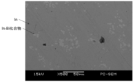
- FIG. 1 shows an image of a COMPO image obtained with an electron microscope (SEM) for an In sputtering target containing 5 atomic% Bi.
- SEM electron microscope
- the element distribution image by EPMA is originally a color image, but is shown in a photograph converted into a black and white image. In the photograph, the whiter, the higher the concentration of Bi element.
- the COMPO image related to In and Bi it is possible to observe a state in which the In—Bi compound in the grayish white portion is dispersed and distributed in the gray In base. .
- the grayish white part is indicated by an arrow “In-Bi compound”.
- ⁇ Measurement of oxygen concentration> About 1 g was sampled from the surface of the produced sputtering target, the surface was etched with aqua regia for about 1 minute, washed with pure water, and the oxygen concentration was measured by gas analysis. ⁇ Analysis of XRD diffraction measurement results> The surface of the produced sputtering target was measured in the range of 2 ⁇ 5 to 80 ° with an XRD apparatus (RINT-Ultima / PC) manufactured by Rigaku Corporation. In Table 1, the case where a peak derived from a Bi, Sb, Sn, and Zn added element appears was “present”, and the case where a peak was not present was “absent”.
- the number of abnormal discharges was measured as follows, and the surface state after this measurement was observed.
- the measurement results are shown in the “abnormal discharge (times / h)” column and “presence / absence of surface roughness after sputtering” column in Tables 3 and 4 below.
- ⁇ Measurement of abnormal discharge times> Sputtering was performed for 12 hours under the above conditions, and the number of abnormal discharges was measured by an arc count function provided in the DC power supply. Thereafter, the sputtering chamber was opened, and particles in the chamber were confirmed.
- the thickness of the In film obtained under the above film formation conditions was measured, and the presence or absence of hillocks (island state) was confirmed on the surface of the In film.
- the observation results are shown in the “film thickness (nm)” column and the “in hillock presence / absence” column of Tables 3 and 4.
- FE-SEM field emission scanning electron microscope
- the In sputtering targets of Comparative Examples 1 and 2 were based on the prior art, and when they were used to form a film, In hillocks were generated because the target contained no additive elements.
- the In sputtering target of Comparative Example 3 has a small amount of additive element Bi
- the In sputtering target of Comparative Example 4 has a small amount of additive element Zn
- the In sputtering target of Comparative Example 5 has an amount of additive element Sb.
- the In sputtering target of Comparative Example 6 since the amount of the additive element Sn was small, no abnormal discharge was observed during sputtering, but In hillocks were generated. None of the In films formed using the In sputtering targets of Comparative Examples 1 to 6 showed improvement in film quality.
- the In film formed with an In sputtering target having a composition contains one or more elements selected from Bi, Sb, Sn, and Zn in a total amount of 0.5 to 10.0 atomic%, with the balance being In. It was confirmed that the film composition was improved and a uniform In film was obtained. It has been found that the In film according to the present invention is suitable for forming a light absorption layer of a CIGS thin solar cell.
Landscapes
- Chemical & Material Sciences (AREA)
- Chemical Kinetics & Catalysis (AREA)
- Engineering & Computer Science (AREA)
- Materials Engineering (AREA)
- Mechanical Engineering (AREA)
- Metallurgy (AREA)
- Organic Chemistry (AREA)
- Physical Vapour Deposition (AREA)
- Photovoltaic Devices (AREA)
Abstract
Bi、Sb、Sn、Znから選択された1種以上の元素を、合計で0.5~10.0原子%含有し、残部がIn及び不可避不純物からなる成分組成を有するInスパッタリングターゲットを提供する。
Description
本発明は、光吸収層としてCu-In-Ga-Se四元系合金膜を有するCIGS系化合物薄膜太陽電池の製造に際して、Cu-In-Ga-Se四元系合金膜を形成するときに使用するInスパッタリングターゲット及びその製造方法に関し、さらに、そのInスパッタリングターゲットを用いたスパッタリングで成膜されたIn薄膜に関する。
本願は、2013年10月7日に、日本に出願された特願2013-209977号に基づき優先権を主張し、その内容をここに援用する。
本願は、2013年10月7日に、日本に出願された特願2013-209977号に基づき優先権を主張し、その内容をここに援用する。
近年、化合物半導体による薄膜太陽電池が実用に供せられている。この化合物半導体による薄膜太陽電池の製造においては、先ず、ソーダライムガラス基板上に、Mo電極層が形成され、このMo電極層上に、Cu-In-Ga-Se四元系合金膜からなる光吸収層が形成され、このCu-In-Ga-Se四元系合金膜からなる光吸収層上に、ZnS、CdSなどからなるバッファ層が形成され、さらに、このバッファ層上に、透明電極層が形成される。CIGS系化合物薄膜太陽電池は、この様な基本構造を有している。
上記のCu-In-Ga-Se四元系合金膜からなる光吸収層の形成方法としては、蒸着法により成膜する方法が知られており、この方法により得られたCu-In-Ga-Se四元系合金膜からなる光吸収層は、高いエネルギー変換効率が得られるという利点もあるが、この蒸着法によると、成膜速度が遅く、大面積の化合物薄膜を成膜する場合には、膜厚の面内分布の均一性が不足している。そのために、セレン化法によって、Cu-In-Ga-Se四元系合金膜からなる光吸収層を形成する方法が提案されている。
上記のCu-In-Ga-Se四元系合金膜をセレン化法で成膜する方法として、先ず、Inスパッタリングターゲットを使用したスパッタリングにより、Mo電極層上に、In膜を成膜し、このIn膜の上に、Cu-Ga二元系合金スパッタリングターゲットを使用してスパッタリングすることにより、Cu-Ga二元系合金膜を成膜し、ここで得られたIn膜及びCu-Ga二元系合金膜からなる積層膜、即ち、前駆体であるプリカーサー膜が形成される。このプリカーサー膜を、Se雰囲気中で熱処理して、Cu-In-Ga-Se四元系合金膜を形成する方法が提案されている(例えば、特許文献1を参照)。
一方、Inスパッタリングターゲットを使用したスパッタリングにより、In膜を形成する際、低融点で表面張力が大きいというInの物性に起因して、Inが粒状に成長してしまい、不連続に隙間を有した粗い、島状のIn膜(以下、ヒロックという)が表面に生成されることが報告されている(例えば、非特許文献1、2を参照)。
Hyenwook Park, etc. "Effect of precursor structure on Cu(InGa)Se2 formation by reactive annealing" Thin Solid Film 519 (2011) 7245-7249, Fig.2(a), (c) [journal homepage: www.elesevier.com/locate/tsf]
S. Merdes, etc. "Influence of precursor stacking on the absorber growth in Cu(InGa)Se2 based solar cells prepared by a rapid thermal process" Thin Solid Film 519 (2011) 7189-7192, Fig.1 (a) [journal homepage: www.elesevier.com/locate/tsf]
上述のように、In膜をスパッタリング法で形成すると、Inが島状に凝集して不連続層が形成されるようになり、例えば、Cu-Ga合金膜上にIn膜を積層する場合には、Inで覆われる部分と覆われない部分が形成されるようになる。この様なInのヒロックが形成されると、その後のセレン化処理時に、Inのない箇所がCuリッチとなって、低抵抗のCu-Se化合物が局所的に生成されることになる。結果的に、光吸収層の成分組成にばらつきが生じ、太陽電池の性能低下をもたらす。
そこで、本発明は、スパッタリング法によってIn膜を成膜したときにInのヒロックを防止でき、薄膜太陽電池におけるCIGS系光吸収層の形成に好適なInスパッタリングターゲットを提供することを目的とする。さらに、本発明は、このInスパッタリングターゲットを用いたスパッタリングで成膜され、Inヒロックの形成を防止して膜質改善した、面内均一性を有するIn膜を提供することを目的とする。
本発明者らは、In膜を成膜時に生じるInヒロックの形成を防止するには、下地膜のCuGa膜、或いは、Cu又はMo膜へのInの濡れ性を改善することにより解決できることに着目し、検討の結果、Inに、Bi、Sb、Sn、Znを添加すると、この濡れ性を改善できることが判明した。
そこで、Inを主成分とし、Bi、Sb、Sn、Znから選択された元素を、少量添加したInスパッタリングターゲットを種々作製し、これらのInスパッタリングターゲットを用いて、直流(DC)スパッタリングで、In膜を成膜したところ、In膜の濡れ性が改善されて、ヒロックは、形成されず、面内均一性を有するIn膜が得られることが確認された。
したがって、本発明は、上記知見から得られたものであり、前記課題を解決するために以下の構成の態様を有する。
(1)Bi、Sb、Sn、Znから選択された1種以上の元素を、合計で0.5~10.0原子%含有し、残部がIn及び不可避不純物からなる成分組成を有することを特徴とするInスパッタリングターゲット。
(2)スパッタリングターゲット中の酸素濃度が0.04質量%以下であることを特徴とする前記(1)に記載のInスパッタリングターゲット。
(3)スパッタリングターゲット中のBi、Sb、Sn、Znから選択された1種以上を含む合金相の最大粒径が50μm以下であることを特徴とする前記(1)に記載のInスパッタリングターゲット。
(4)Bi、Sb、Sn、Znから選択される1種以上の元素を、合計で0.5~10.0原子%含有し、残部がIn及び不可避不純物からなる成分組成を有することを特徴とするCIGS太陽電製造用In膜。
(1)Bi、Sb、Sn、Znから選択された1種以上の元素を、合計で0.5~10.0原子%含有し、残部がIn及び不可避不純物からなる成分組成を有することを特徴とするInスパッタリングターゲット。
(2)スパッタリングターゲット中の酸素濃度が0.04質量%以下であることを特徴とする前記(1)に記載のInスパッタリングターゲット。
(3)スパッタリングターゲット中のBi、Sb、Sn、Znから選択された1種以上を含む合金相の最大粒径が50μm以下であることを特徴とする前記(1)に記載のInスパッタリングターゲット。
(4)Bi、Sb、Sn、Znから選択される1種以上の元素を、合計で0.5~10.0原子%含有し、残部がIn及び不可避不純物からなる成分組成を有することを特徴とするCIGS太陽電製造用In膜。
上記の本発明の態様のInスパッタリングターゲット(以下、本願発明のInスパッタリングターゲットと称する)においては、Bi、Sb、Znから選択された1種以上の元素の添加について、合計で0.5~10.0原子%含有するとしているが、この添加量を範囲限定している理由は、この添加量が、10.0原子%を超えて多くなると、CIGS系薄膜太陽電池の変換効率が低下し、一方、その添加量が、0.5原子%未満であると、膜中のInヒロック発生、即ち、島状Inの発生の抑制ができないからである。
また、スパッタリングターゲット中のBi、Sb、Sn、Znから選択された1種以上の元素を含む合金相(例えば、これら元素の1種とInとの化合物(BiIn2、Bi3In5、BiIn、InSb)、或いは、ZnとSbの化合物や各元素間の固溶体など。以下、添加元素含有合金相とする)の最大粒径が50μm以下としている。ここで、Bi、Sb、Sn、Znから選択された1種以上の元素が添加されたInスパッタリングターゲットを用いて直流(DC)スパッタリングするとき、添加元素含有合金相の粒径の大きさは、異常放電、ノジュールの発生の要因となるが、最大粒径が50μm以下であれば、過度な異常放電は発生しない。
さらに、スパッタリングターゲット中の酸素含有量は、スパッタ後のターゲット表面の荒れ発生の原因である、スパッタリング時の異常放電の発生を抑制する上では、できるだけ少ないことが好ましく、本発明では、酸素含有量を0.04質量%以下とした。さらに、望ましくは、酸素含有量は0.03質量%以下が良い。
さらに、スパッタリングターゲット中の酸素含有量は、スパッタ後のターゲット表面の荒れ発生の原因である、スパッタリング時の異常放電の発生を抑制する上では、できるだけ少ないことが好ましく、本発明では、酸素含有量を0.04質量%以下とした。さらに、望ましくは、酸素含有量は0.03質量%以下が良い。
以上の様に、本発明のInスパッタリングターゲットは、Bi、Sb、Sn、Znから選択された1種以上の元素が、合計で0.5~10.0原子%含有し、残部がIn及び不可避不純物からなる成分組成を有することを特徴としており、このInスパッタリングターゲットを用いてスパッタリングすれば、Bi、Sb、Sn、Znから選択された1種以上の元素が、合計で0.5~10.0原子%含有し、残部がIn及び不可避不純物からなる成分組成を有するIn膜を成膜することができ、Bi、Sb、Sn、Znから選択された1種以上の元素が添加されることで、膜質が改善され、均一なIn膜が得られるようになり、CIGS系化合物薄膜太陽電池における光吸収層の形成に有効であって、かつ、インライン方式のスパッタリングにも適用が可能となり、薄膜太陽電池の生産性向上に寄与する。
つぎに、この発明のInスパッタリングターゲット及びその製造方法、さらには、In薄膜について、以下に、実施例により具体的に説明する。
〔実施例〕
先ず、Inスパッタリングターゲットを製造するために、ターゲット製造原料として、In(純度4N以上)、Bi(純度4N以上)、Sb(純度4N以上)、Sn(純度4N以上)、Zn(純度4N以上)を用意した。ここで、Bi、Sb、Sn、Znに関しては、製造原料としてインゴットでも良いが、溶解のしやすさから、粉末のものを用意した。下記の表1に示されるように、Inと、添加元素としてのBi、Sb、Sn、Znの各粉末とをそれぞれ秤量した。なお、表1には、添加元素の量(質量%)のみが示されているが、Inの量は、その残部であるため、表示されていない。
先ず、Inスパッタリングターゲットを製造するために、ターゲット製造原料として、In(純度4N以上)、Bi(純度4N以上)、Sb(純度4N以上)、Sn(純度4N以上)、Zn(純度4N以上)を用意した。ここで、Bi、Sb、Sn、Znに関しては、製造原料としてインゴットでも良いが、溶解のしやすさから、粉末のものを用意した。下記の表1に示されるように、Inと、添加元素としてのBi、Sb、Sn、Znの各粉末とをそれぞれ秤量した。なお、表1には、添加元素の量(質量%)のみが示されているが、Inの量は、その残部であるため、表示されていない。
次いで、秤量された各原料粉末を、カーボン製のるつぼに入れ、真空中にて、高周波誘導加熱により加熱を行い、溶解する。なお、真空中で加熱する代わりに、大気中或いは非酸化性雰囲気で加熱されてもよい。そして、各添加元素が溶けた時点の温度を5分間保持した後、予め、堰を設けた125mm径のCuバッキングプレート上に鋳込む。鋳造後のバッキングプレートとの密着性を向上させるため、Cuバッキングプレート表面は、あらかじめ鋳込みを行う組成のIn合金で濡らしておくことが好ましい。ここで、冷却の後、堰を外したうえで、機械加工にて、所定形状に整え、実施例1~29のInスパッタリングターゲットを作製した。なお、本実施例では、Inを溶解したのち、Cuバッキングプレート上で鋳造したが、予めCuバッキングプレート上にIn原料を配置し、Cuバッキングプレートを加熱することにより、Inを溶解し、その後、凝固させてInスパッタリングターゲットを作製することもできる。
〔比較例〕
また、本発明の実施例と比較するため、下記の表2に示すように、実施例の場合と同様の手法により、添加元素を含まないInのみの比較例1及び2のInスパッタリングターゲットと、Bi:0.05原子%を添加した比較例3のInスパッタリングターゲットと、Zn:0.07原子%を添加した比較例4のInスパッタリングターゲットと、Sb:0.07原子%を添加した比較例5のInスパッタリングターゲットと、Snを0.05原子%添加した比較例6のInスパッタリングターゲットをそれぞれ作製した。
また、本発明の実施例と比較するため、下記の表2に示すように、実施例の場合と同様の手法により、添加元素を含まないInのみの比較例1及び2のInスパッタリングターゲットと、Bi:0.05原子%を添加した比較例3のInスパッタリングターゲットと、Zn:0.07原子%を添加した比較例4のInスパッタリングターゲットと、Sb:0.07原子%を添加した比較例5のInスパッタリングターゲットと、Snを0.05原子%添加した比較例6のInスパッタリングターゲットをそれぞれ作製した。
作製した実施例及び比較例のInスパッタリングターゲットのターゲット基本特性は、ターゲット組織の平均粒径:200μm以下、表面粗さRa:3μm以下、比抵抗:10-1Ω・cm以下であった。次に、実施例1~29及び比較例3~6のInスパッタリングターゲットについて、添加元素含有合金相の最大粒径を測定した。その測定方法は、以下の様である。
<添加元素含有合金相の最大粒径測定方法>
作製されたスパッタリングターゲットの表面(旋盤加工面)を王水で1分程度エッチングし、純水で洗浄後、電子線マイクロアナライザ(EPMA)によるマッピング分析を、倍率200倍で、表面上の任意の5箇所で観測した。明確な組織が見えない場合には、王水のエッチングを追加で行った。ここで、EPMAの1画像から観察される添加元素成分のうち、最も大きい領域に係る最大径を、添加元素含有合金相の最大粒径とした。その測定結果が、下記の表1に示されている。
作製されたスパッタリングターゲットの表面(旋盤加工面)を王水で1分程度エッチングし、純水で洗浄後、電子線マイクロアナライザ(EPMA)によるマッピング分析を、倍率200倍で、表面上の任意の5箇所で観測した。明確な組織が見えない場合には、王水のエッチングを追加で行った。ここで、EPMAの1画像から観察される添加元素成分のうち、最も大きい領域に係る最大径を、添加元素含有合金相の最大粒径とした。その測定結果が、下記の表1に示されている。
なお、参考例として、Biを5原子%含有させたInスパッタリングターゲットについて、電子顕微鏡(SEM)で取得したCOMPO像の画像を、図1に示した。EPMAによる元素分布像は、本来カラー像であるが、白黒像に変換した写真で示しているため、その写真中において、白いほど、Bi元素の濃度が高いことを表している。具体的には、図1の画像のように、In及びBiに関するCOMPO像では、灰色を示すInの素地中に、灰白色部分のIn-Bi化合物が分散分布している様子を観察することができる。なお、灰白色部分には、「In-Bi化合物」と矢示されている。
<酸素濃度の測定>
作製されたスパッタリングターゲットの表面から1g程度サンプリングを行い、表面を王水で1分程度エッチングし、純水で洗浄後、ガス分析により酸素濃度を測定した。
<XRD回折測定結果の解析>
作製されたスパッタリングターゲットの表面を理学電気社製XRD装置(RINT-Ultima/PC)により、2θ=5~80°の範囲で測定した。表1においては、Bi、Sb、Sn、Zn添加元素単体に由来するピークが現れた場合を「有」とし、現れない場合を「無」とした。
作製されたスパッタリングターゲットの表面から1g程度サンプリングを行い、表面を王水で1分程度エッチングし、純水で洗浄後、ガス分析により酸素濃度を測定した。
<XRD回折測定結果の解析>
作製されたスパッタリングターゲットの表面を理学電気社製XRD装置(RINT-Ultima/PC)により、2θ=5~80°の範囲で測定した。表1においては、Bi、Sb、Sn、Zn添加元素単体に由来するピークが現れた場合を「有」とし、現れない場合を「無」とした。


次に、上述した実施例1~29及び比較例1~6のInスパッタリングターゲットを用いて、以下の成膜条件により、In膜の成膜試験を行った。In膜の膜厚は、300~500nmである。
<成膜条件>
・基板:ガラス基板
・基板サイズ:20mm角
・電源:DC500W
・全圧:0.15Pa
・スパッタリングガス:Ar=30sccm
・ターゲット-基板(TS)距離:70mm
<成膜条件>
・基板:ガラス基板
・基板サイズ:20mm角
・電源:DC500W
・全圧:0.15Pa
・スパッタリングガス:Ar=30sccm
・ターゲット-基板(TS)距離:70mm
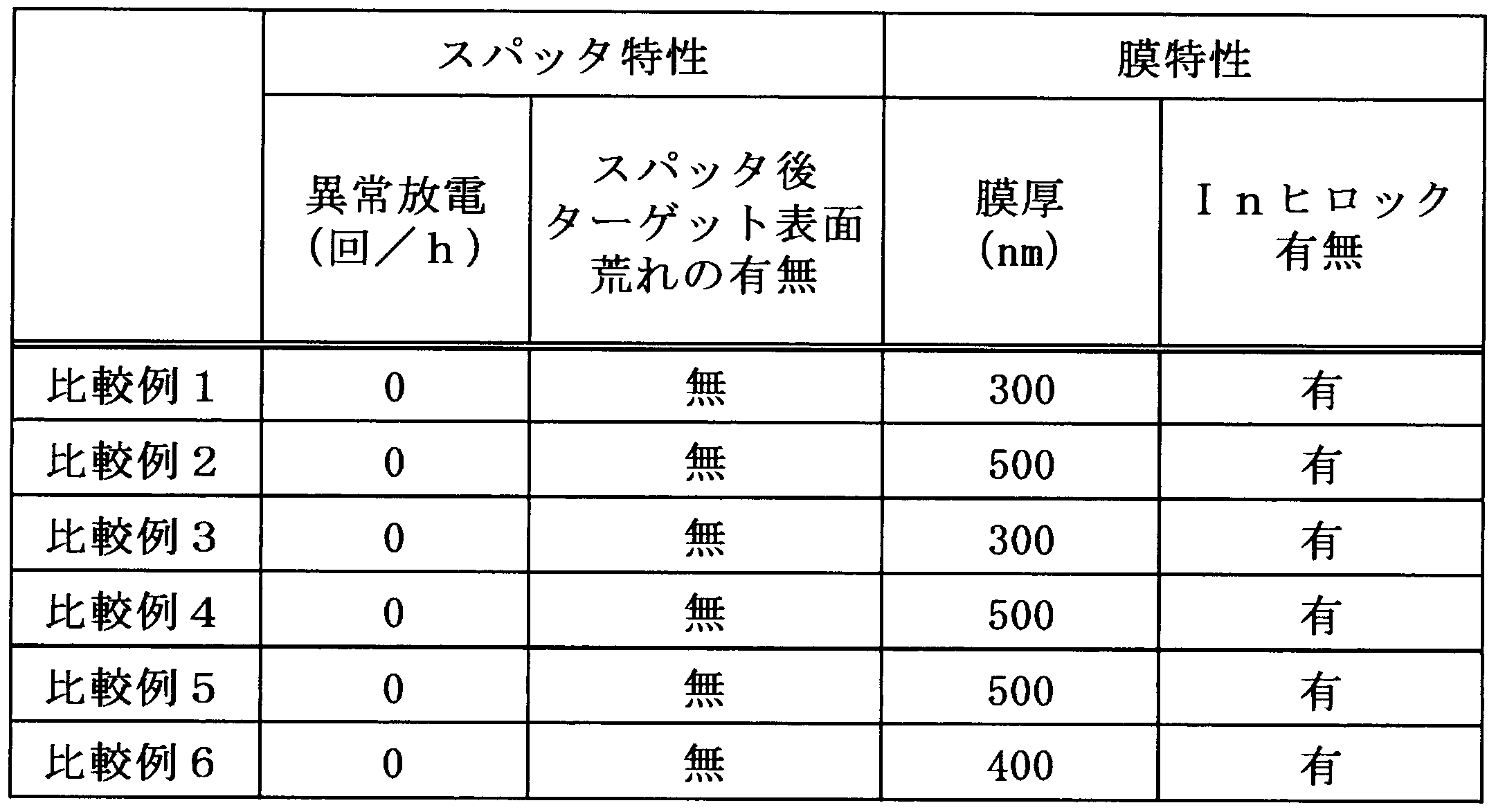
上記の成膜条件に従った成膜試験により、以下の様にして、異常放電回数を測定し、この測定後における表面状態の観察を行った。この測定結果が、下記の表3及び表4の「異常放電(回/h)」欄と「スパッタ後ターゲット表面荒れの有無」欄に示されている。
<異常放電回数の測定>
上述の条件において12時間のスパッタリングを行い、DC電源装置に備えられているアークカウント機能により異常放電の回数を計測した。その後、スパッタチャンバーを開放し、チャンバー内のパーティクルを確認した。
<スパッタ後のターゲット表面状態の観察>
異常放電回数の測定後のターゲット表面を観察し、エロージョン部が凸凹に荒れている場合を、荒れ「有」とし、荒れのない場合を、荒れ「無」とした。
<異常放電回数の測定>
上述の条件において12時間のスパッタリングを行い、DC電源装置に備えられているアークカウント機能により異常放電の回数を計測した。その後、スパッタチャンバーを開放し、チャンバー内のパーティクルを確認した。
<スパッタ後のターゲット表面状態の観察>
異常放電回数の測定後のターゲット表面を観察し、エロージョン部が凸凹に荒れている場合を、荒れ「有」とし、荒れのない場合を、荒れ「無」とした。
上記の成膜条件で得られたIn膜の膜厚を測定し、さらに、そのIn膜の表面について、ヒロック(島状態)の有無を確認した。この観察結果が、表3及び表4の「膜厚(nm)」欄と、「Inヒロック有無」欄とに示されている。
<ヒロックの評価方法>
得られたIn膜を取り出し、電界放射型走査電子顕微鏡(FE-SEM)にて膜表面のInヒロックの有無を確認した。In膜にInヒロックが現れるものを「有」、現れないものを「無」とした。
<ヒロックの評価方法>
得られたIn膜を取り出し、電界放射型走査電子顕微鏡(FE-SEM)にて膜表面のInヒロックの有無を確認した。In膜にInヒロックが現れるものを「有」、現れないものを「無」とした。
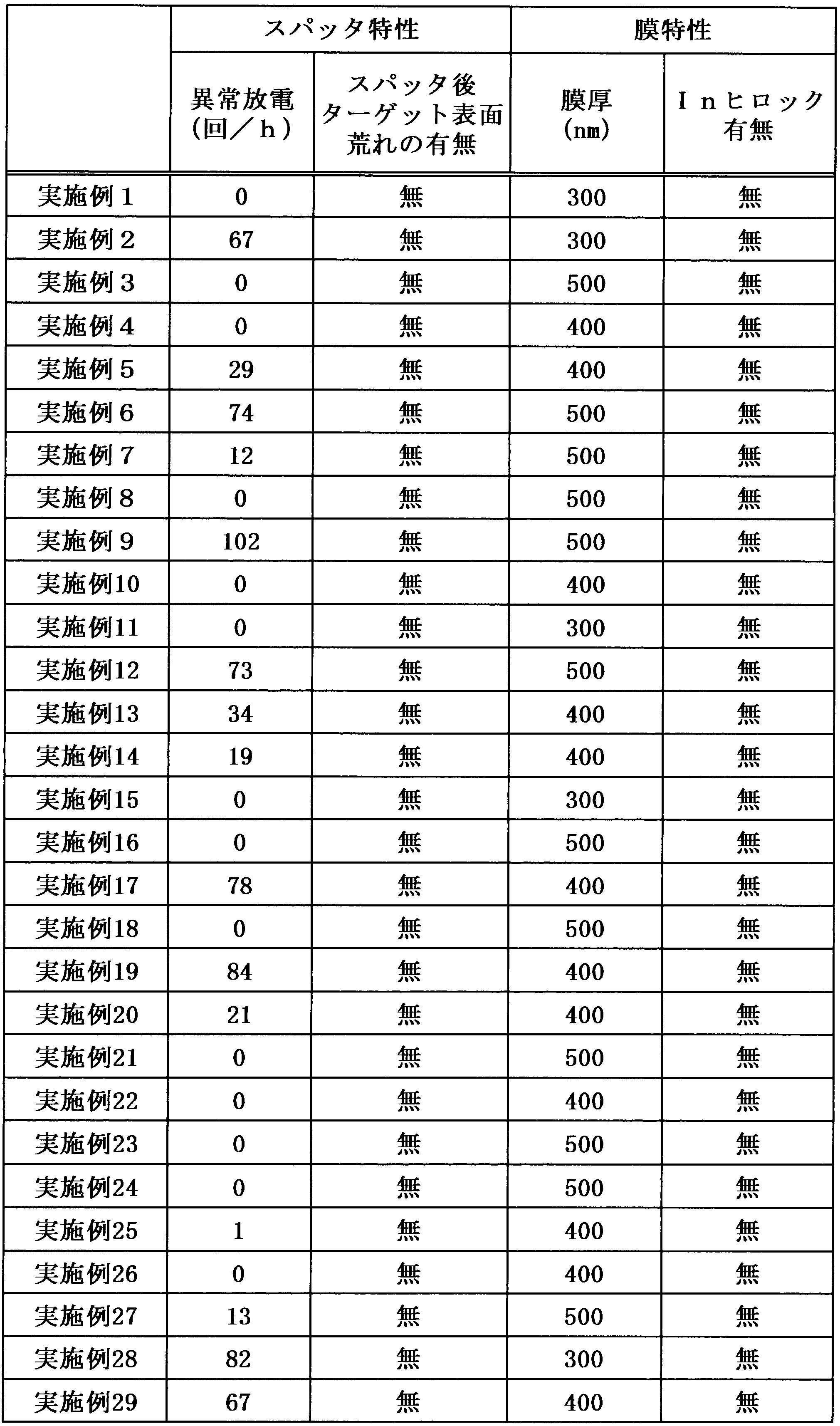
以上の表3によれば、実施例1~29のInスパッタリングターゲットを用いたスパッタリングで成膜されたIn膜のいずれも、Inヒロックが無いことが確認され、平坦で均一なIn膜が得られた。また、実施例1、3、4、8、10、11、15、16、18、21~24、25、26のInスパッタリングターゲットを用いてスパッタリングを行った場合には、添加元素含有合金相の最大粒径が小さいため、異常放電の発生が皆無であることが分かった。なお、実施例2、5~3、9、12~14、17、19、20、27~29のInスパッタリングターゲットを用いてスパッタリングを行った場合には、添加元素含有合金相の最大粒径が大きいため、異常放電が発生したが、これは、成膜に影響するものではなく、均一なIn膜が得られた。
一方、比較例1、2のInスパッタリングターゲットは、従来技術による場合であって、それらを用いて成膜すると、ターゲット中には、添加元素が含まれていないので、Inヒロックが発生した。また、比較例3のInスパッタリングターゲットでは、添加元素Biの量が少なく、比較例4のInスパッタリングターゲットでは、添加元素Znの量が少なく、比較例5のInスパッタリングターゲットでは、添加元素Sbの量が少なく、さらには比較例6のInスパッタリングターゲットでは、添加元素Snの量が少ないため、スパッタリング時には、異常放電の発生が見られなかったものの、Inヒロックが発生した。比較例1~6のInスパッタリングターゲットを用いて成膜されたIn膜のいずれも、膜質改善が見られなかった。
以上の様に、本発明による、Bi、Sb、Sn、Znから選択された1種以上の元素が、合計で0.5~10.0原子%含有し、残部がIn及び不可避不純物からなる成分組成を有するInスパッタリングターゲットで成膜されたIn膜は、Bi、Sb、Sn、Znから選択される1種以上の元素が、合計で0.5~10.0原子%含有し、残部がIn及び不可避不純物からなる成分組成を有し、膜質が改善され、均一なIn膜が得られることを確認した。本発明によるIn膜は、CIGS系薄太陽電池の光吸収層の形成に好適なものであることが分かった。
セレン化法によって、Cu-In-Ga-Se四元系合成膜からなる光吸収層を形成するのに適したInスパッタリングターゲットを提供することにより、その光吸収層を備える太陽電池の性能を向上させることができる。
1 In
2 In-Bi化合物
2 In-Bi化合物
Claims (4)
- Bi、Sb、Sn、Znから選択された1種以上の元素を合計で0.5~10.0原子%含有し、残部がIn及び不可避不純物からなる成分組成を有することを特徴とするInスパッタリングターゲット。
- スパッタリングターゲット中の酸素濃度が0.04質量%以下であることを特徴とする請求項1に記載のInスパッタリングターゲット。
- スパッタリングターゲット中のBi、Sb、Sn、Znから選択された1種以上を含む合金相の最大粒径が50μm以下であることを特徴とする請求項1に記載のInスパッタリングターゲット。
- Bi、Sb、Sn、Znから選択される1種以上の元素を、合計で0.5~10.0原子%含有し、残部がIn及び不可避不純物からなる成分組成を有することを特徴とするCIGS太陽電池製造用In膜。
Applications Claiming Priority (2)
| Application Number | Priority Date | Filing Date | Title |
|---|---|---|---|
| JP2013-209977 | 2013-10-07 | ||
| JP2013209977A JP6217295B2 (ja) | 2013-10-07 | 2013-10-07 | Inスパッタリングターゲット |
Publications (1)
| Publication Number | Publication Date |
|---|---|
| WO2015053265A1 true WO2015053265A1 (ja) | 2015-04-16 |
Family
ID=52813081
Family Applications (1)
| Application Number | Title | Priority Date | Filing Date |
|---|---|---|---|
| PCT/JP2014/076811 Ceased WO2015053265A1 (ja) | 2013-10-07 | 2014-10-07 | In膜、In膜を成膜するためのInスパッタリングターゲット及びその製造方法 |
Country Status (3)
| Country | Link |
|---|---|
| JP (1) | JP6217295B2 (ja) |
| TW (1) | TW201529862A (ja) |
| WO (1) | WO2015053265A1 (ja) |
Families Citing this family (2)
| Publication number | Priority date | Publication date | Assignee | Title |
|---|---|---|---|---|
| WO2017099215A1 (ja) * | 2015-12-11 | 2017-06-15 | 旭硝子株式会社 | スパッタリングターゲット、積層体、複層体、および積層体の製造方法 |
| CN107083509B (zh) * | 2017-03-16 | 2018-06-19 | 宁波新瑞清科金属材料有限公司 | 用于igbt散热的复合式液态金属热界面材料 |
Citations (3)
| Publication number | Priority date | Publication date | Assignee | Title |
|---|---|---|---|---|
| JP2000121824A (ja) * | 1998-10-14 | 2000-04-28 | Ulvac Japan Ltd | 亜鉛/インジウム系bm膜、及びbm膜製造方法 |
| JP2004068054A (ja) * | 2002-08-02 | 2004-03-04 | Idemitsu Kosan Co Ltd | スパッタリングターゲット及び焼結体それらを利用して製造した導電膜。 |
| JP2012172265A (ja) * | 2011-02-22 | 2012-09-10 | Heraeus Materials Technology Gmbh & Co Kg | 管状スパッタターゲット |
Family Cites Families (6)
| Publication number | Priority date | Publication date | Assignee | Title |
|---|---|---|---|---|
| JPH11236664A (ja) * | 1998-02-24 | 1999-08-31 | Mitsui Chem Inc | スパッタリング用ターゲットのバッキングプレート |
| US8080141B2 (en) * | 2008-11-18 | 2011-12-20 | Guardian Industries Corp. | ITO-coated article and/or method of making the same via heat treating |
| US9103000B2 (en) * | 2009-11-25 | 2015-08-11 | Zetta Research and Development LLC—AQT Series | Low melting point sputter targets for chalcogenide photovoltaic applications and methods of manufacturing the same |
| JP5165100B1 (ja) * | 2011-11-01 | 2013-03-21 | 三菱マテリアル株式会社 | スパッタリングターゲット及びその製造方法 |
| JP5424140B2 (ja) * | 2012-04-13 | 2014-02-26 | 三菱マテリアル株式会社 | 透明導電膜形成用スパッタリングターゲット |
| CN103194722B (zh) * | 2013-03-28 | 2016-04-27 | 深圳首创新能源股份有限公司 | 制造太阳能电池的方法 |
-
2013
- 2013-10-07 JP JP2013209977A patent/JP6217295B2/ja not_active Expired - Fee Related
-
2014
- 2014-10-07 WO PCT/JP2014/076811 patent/WO2015053265A1/ja not_active Ceased
- 2014-10-07 TW TW103134885A patent/TW201529862A/zh unknown
Patent Citations (3)
| Publication number | Priority date | Publication date | Assignee | Title |
|---|---|---|---|---|
| JP2000121824A (ja) * | 1998-10-14 | 2000-04-28 | Ulvac Japan Ltd | 亜鉛/インジウム系bm膜、及びbm膜製造方法 |
| JP2004068054A (ja) * | 2002-08-02 | 2004-03-04 | Idemitsu Kosan Co Ltd | スパッタリングターゲット及び焼結体それらを利用して製造した導電膜。 |
| JP2012172265A (ja) * | 2011-02-22 | 2012-09-10 | Heraeus Materials Technology Gmbh & Co Kg | 管状スパッタターゲット |
Also Published As
| Publication number | Publication date |
|---|---|
| JP6217295B2 (ja) | 2017-10-25 |
| JP2015074788A (ja) | 2015-04-20 |
| TW201529862A (zh) | 2015-08-01 |
Similar Documents
| Publication | Publication Date | Title |
|---|---|---|
| JP5923569B2 (ja) | Cu−Ga系スパッタリングターゲット | |
| US9103000B2 (en) | Low melting point sputter targets for chalcogenide photovoltaic applications and methods of manufacturing the same | |
| JP5202643B2 (ja) | Cu−Ga合金焼結体スパッタリングターゲット及び同ターゲットの製造方法 | |
| JP5730788B2 (ja) | スパッタリングターゲット及びスパッタリングターゲットの製造方法 | |
| US7717987B2 (en) | Coating material based on a copper-indium-gallium alloy, in particular for the production of sputter targets, tubular cathodes and the like | |
| JP2012233230A (ja) | スパッタリングターゲット及びその製造方法 | |
| US20150014156A1 (en) | Sputtering target and process for producing same | |
| WO2013069710A1 (ja) | スパッタリングターゲットおよびその製造方法 | |
| WO2012042959A1 (ja) | Cu-In-Ga-Se四元系合金スパッタリングターゲット | |
| TWI647319B (zh) | Cu-Ga合金濺鍍靶及其製造方法 | |
| JP6217295B2 (ja) | Inスパッタリングターゲット | |
| CN106471150B (zh) | 溅射靶及其制造方法 | |
| JP2008081794A (ja) | アルミニウム合金および薄膜系太陽電池基板 | |
| WO2012098722A1 (ja) | Cu-Gaターゲット及びその製造方法並びにCu-Ga系合金膜からなる光吸収層及び同光吸収層を用いたCIGS系太陽電池 | |
| JP5871106B2 (ja) | In合金スパッタリングターゲット、その製造方法及びIn合金膜 | |
| WO2014024975A1 (ja) | スパッタリングターゲット及びその製造方法 | |
| JP2012079997A (ja) | 化合物半導体薄膜太陽電池用光吸収層の製造方法、およびIn−Cu合金スパッタリングターゲット | |
| CN105473758B (zh) | 溅射靶及其制造方法 | |
| WO2016047556A1 (ja) | スパッタリングターゲット及びその製造方法 | |
| TW201514328A (zh) | 濺鍍靶材及其製造方法 |
Legal Events
| Date | Code | Title | Description |
|---|---|---|---|
| 121 | Ep: the epo has been informed by wipo that ep was designated in this application |
Ref document number: 14852534 Country of ref document: EP Kind code of ref document: A1 |
|
| NENP | Non-entry into the national phase |
Ref country code: DE |
|
| 122 | Ep: pct application non-entry in european phase |
Ref document number: 14852534 Country of ref document: EP Kind code of ref document: A1 |