WO2015046334A1 - 半導体素子三次元実装用充填材 - Google Patents
半導体素子三次元実装用充填材 Download PDFInfo
- Publication number
- WO2015046334A1 WO2015046334A1 PCT/JP2014/075433 JP2014075433W WO2015046334A1 WO 2015046334 A1 WO2015046334 A1 WO 2015046334A1 JP 2014075433 W JP2014075433 W JP 2014075433W WO 2015046334 A1 WO2015046334 A1 WO 2015046334A1
- Authority
- WO
- WIPO (PCT)
- Prior art keywords
- filler
- curable composition
- semiconductor
- semiconductor element
- weight
- Prior art date
- Legal status (The legal status is an assumption and is not a legal conclusion. Google has not performed a legal analysis and makes no representation as to the accuracy of the status listed.)
- Ceased
Links
Images

Classifications
-
- C—CHEMISTRY; METALLURGY
- C08—ORGANIC MACROMOLECULAR COMPOUNDS; THEIR PREPARATION OR CHEMICAL WORKING-UP; COMPOSITIONS BASED THEREON
- C08G—MACROMOLECULAR COMPOUNDS OBTAINED OTHERWISE THAN BY REACTIONS ONLY INVOLVING UNSATURATED CARBON-TO-CARBON BONDS
- C08G59/00—Polycondensates containing more than one epoxy group per molecule; Macromolecules obtained by polymerising compounds containing more than one epoxy group per molecule using curing agents or catalysts which react with the epoxy groups
- C08G59/18—Macromolecules obtained by polymerising compounds containing more than one epoxy group per molecule using curing agents or catalysts which react with the epoxy groups ; e.g. general methods of curing
- C08G59/20—Macromolecules obtained by polymerising compounds containing more than one epoxy group per molecule using curing agents or catalysts which react with the epoxy groups ; e.g. general methods of curing characterised by the epoxy compounds used
- C08G59/22—Di-epoxy compounds
- C08G59/24—Di-epoxy compounds carbocyclic
- C08G59/245—Di-epoxy compounds carbocyclic aromatic
-
- C—CHEMISTRY; METALLURGY
- C08—ORGANIC MACROMOLECULAR COMPOUNDS; THEIR PREPARATION OR CHEMICAL WORKING-UP; COMPOSITIONS BASED THEREON
- C08G—MACROMOLECULAR COMPOUNDS OBTAINED OTHERWISE THAN BY REACTIONS ONLY INVOLVING UNSATURATED CARBON-TO-CARBON BONDS
- C08G59/00—Polycondensates containing more than one epoxy group per molecule; Macromolecules obtained by polymerising compounds containing more than one epoxy group per molecule using curing agents or catalysts which react with the epoxy groups
- C08G59/18—Macromolecules obtained by polymerising compounds containing more than one epoxy group per molecule using curing agents or catalysts which react with the epoxy groups ; e.g. general methods of curing
- C08G59/20—Macromolecules obtained by polymerising compounds containing more than one epoxy group per molecule using curing agents or catalysts which react with the epoxy groups ; e.g. general methods of curing characterised by the epoxy compounds used
- C08G59/22—Di-epoxy compounds
- C08G59/226—Mixtures of di-epoxy compounds
-
- C—CHEMISTRY; METALLURGY
- C08—ORGANIC MACROMOLECULAR COMPOUNDS; THEIR PREPARATION OR CHEMICAL WORKING-UP; COMPOSITIONS BASED THEREON
- C08G—MACROMOLECULAR COMPOUNDS OBTAINED OTHERWISE THAN BY REACTIONS ONLY INVOLVING UNSATURATED CARBON-TO-CARBON BONDS
- C08G59/00—Polycondensates containing more than one epoxy group per molecule; Macromolecules obtained by polymerising compounds containing more than one epoxy group per molecule using curing agents or catalysts which react with the epoxy groups
- C08G59/18—Macromolecules obtained by polymerising compounds containing more than one epoxy group per molecule using curing agents or catalysts which react with the epoxy groups ; e.g. general methods of curing
- C08G59/20—Macromolecules obtained by polymerising compounds containing more than one epoxy group per molecule using curing agents or catalysts which react with the epoxy groups ; e.g. general methods of curing characterised by the epoxy compounds used
- C08G59/22—Di-epoxy compounds
- C08G59/24—Di-epoxy compounds carbocyclic
-
- C—CHEMISTRY; METALLURGY
- C08—ORGANIC MACROMOLECULAR COMPOUNDS; THEIR PREPARATION OR CHEMICAL WORKING-UP; COMPOSITIONS BASED THEREON
- C08G—MACROMOLECULAR COMPOUNDS OBTAINED OTHERWISE THAN BY REACTIONS ONLY INVOLVING UNSATURATED CARBON-TO-CARBON BONDS
- C08G59/00—Polycondensates containing more than one epoxy group per molecule; Macromolecules obtained by polymerising compounds containing more than one epoxy group per molecule using curing agents or catalysts which react with the epoxy groups
- C08G59/18—Macromolecules obtained by polymerising compounds containing more than one epoxy group per molecule using curing agents or catalysts which react with the epoxy groups ; e.g. general methods of curing
- C08G59/40—Macromolecules obtained by polymerising compounds containing more than one epoxy group per molecule using curing agents or catalysts which react with the epoxy groups ; e.g. general methods of curing characterised by the curing agents used
- C08G59/4007—Curing agents not provided for by the groups C08G59/42 - C08G59/66
- C08G59/4064—Curing agents not provided for by the groups C08G59/42 - C08G59/66 sulfur containing compounds
-
- C—CHEMISTRY; METALLURGY
- C08—ORGANIC MACROMOLECULAR COMPOUNDS; THEIR PREPARATION OR CHEMICAL WORKING-UP; COMPOSITIONS BASED THEREON
- C08G—MACROMOLECULAR COMPOUNDS OBTAINED OTHERWISE THAN BY REACTIONS ONLY INVOLVING UNSATURATED CARBON-TO-CARBON BONDS
- C08G59/00—Polycondensates containing more than one epoxy group per molecule; Macromolecules obtained by polymerising compounds containing more than one epoxy group per molecule using curing agents or catalysts which react with the epoxy groups
- C08G59/18—Macromolecules obtained by polymerising compounds containing more than one epoxy group per molecule using curing agents or catalysts which react with the epoxy groups ; e.g. general methods of curing
- C08G59/68—Macromolecules obtained by polymerising compounds containing more than one epoxy group per molecule using curing agents or catalysts which react with the epoxy groups ; e.g. general methods of curing characterised by the catalysts used
- C08G59/687—Macromolecules obtained by polymerising compounds containing more than one epoxy group per molecule using curing agents or catalysts which react with the epoxy groups ; e.g. general methods of curing characterised by the catalysts used containing sulfur
-
- C—CHEMISTRY; METALLURGY
- C08—ORGANIC MACROMOLECULAR COMPOUNDS; THEIR PREPARATION OR CHEMICAL WORKING-UP; COMPOSITIONS BASED THEREON
- C08K—Use of inorganic or non-macromolecular organic substances as compounding ingredients
- C08K3/00—Use of inorganic substances as compounding ingredients
- C08K3/34—Silicon-containing compounds
- C08K3/36—Silica
-
- C—CHEMISTRY; METALLURGY
- C08—ORGANIC MACROMOLECULAR COMPOUNDS; THEIR PREPARATION OR CHEMICAL WORKING-UP; COMPOSITIONS BASED THEREON
- C08K—Use of inorganic or non-macromolecular organic substances as compounding ingredients
- C08K5/00—Use of organic ingredients
- C08K5/54—Silicon-containing compounds
- C08K5/541—Silicon-containing compounds containing oxygen
- C08K5/5425—Silicon-containing compounds containing oxygen containing at least one C=C bond
-
- C—CHEMISTRY; METALLURGY
- C08—ORGANIC MACROMOLECULAR COMPOUNDS; THEIR PREPARATION OR CHEMICAL WORKING-UP; COMPOSITIONS BASED THEREON
- C08L—COMPOSITIONS OF MACROMOLECULAR COMPOUNDS
- C08L63/00—Compositions of epoxy resins; Compositions of derivatives of epoxy resins
-
- H—ELECTRICITY
- H10—SEMICONDUCTOR DEVICES; ELECTRIC SOLID-STATE DEVICES NOT OTHERWISE PROVIDED FOR
- H10W—GENERIC PACKAGES, INTERCONNECTIONS, CONNECTORS OR OTHER CONSTRUCTIONAL DETAILS OF DEVICES COVERED BY CLASS H10
- H10W70/00—Package substrates; Interposers; Redistribution layers [RDL]
- H10W70/01—Manufacture or treatment
- H10W70/05—Manufacture or treatment of insulating or insulated package substrates, or of interposers, or of redistribution layers
- H10W70/093—Connecting or disconnecting other interconnections thereto or therefrom, e.g. connecting bond wires or bumps
-
- H—ELECTRICITY
- H10—SEMICONDUCTOR DEVICES; ELECTRIC SOLID-STATE DEVICES NOT OTHERWISE PROVIDED FOR
- H10W—GENERIC PACKAGES, INTERCONNECTIONS, CONNECTORS OR OTHER CONSTRUCTIONAL DETAILS OF DEVICES COVERED BY CLASS H10
- H10W70/00—Package substrates; Interposers; Redistribution layers [RDL]
- H10W70/60—Insulating or insulated package substrates; Interposers; Redistribution layers
- H10W70/611—Insulating or insulated package substrates; Interposers; Redistribution layers for connecting multiple chips together
- H10W70/614—Insulating or insulated package substrates; Interposers; Redistribution layers for connecting multiple chips together the multiple chips being integrally enclosed
-
- H—ELECTRICITY
- H10—SEMICONDUCTOR DEVICES; ELECTRIC SOLID-STATE DEVICES NOT OTHERWISE PROVIDED FOR
- H10W—GENERIC PACKAGES, INTERCONNECTIONS, CONNECTORS OR OTHER CONSTRUCTIONAL DETAILS OF DEVICES COVERED BY CLASS H10
- H10W72/00—Interconnections or connectors in packages
- H10W72/01—Manufacture or treatment
- H10W72/0198—Manufacture or treatment batch processes
-
- H—ELECTRICITY
- H10—SEMICONDUCTOR DEVICES; ELECTRIC SOLID-STATE DEVICES NOT OTHERWISE PROVIDED FOR
- H10W—GENERIC PACKAGES, INTERCONNECTIONS, CONNECTORS OR OTHER CONSTRUCTIONAL DETAILS OF DEVICES COVERED BY CLASS H10
- H10W74/00—Encapsulations, e.g. protective coatings
- H10W74/01—Manufacture or treatment
- H10W74/014—Manufacture or treatment using batch processing
-
- H—ELECTRICITY
- H10—SEMICONDUCTOR DEVICES; ELECTRIC SOLID-STATE DEVICES NOT OTHERWISE PROVIDED FOR
- H10W—GENERIC PACKAGES, INTERCONNECTIONS, CONNECTORS OR OTHER CONSTRUCTIONAL DETAILS OF DEVICES COVERED BY CLASS H10
- H10W74/00—Encapsulations, e.g. protective coatings
- H10W74/01—Manufacture or treatment
- H10W74/016—Manufacture or treatment using moulds
-
- H—ELECTRICITY
- H10—SEMICONDUCTOR DEVICES; ELECTRIC SOLID-STATE DEVICES NOT OTHERWISE PROVIDED FOR
- H10W—GENERIC PACKAGES, INTERCONNECTIONS, CONNECTORS OR OTHER CONSTRUCTIONAL DETAILS OF DEVICES COVERED BY CLASS H10
- H10W74/00—Encapsulations, e.g. protective coatings
- H10W74/10—Encapsulations, e.g. protective coatings characterised by their shape or disposition
- H10W74/111—Encapsulations, e.g. protective coatings characterised by their shape or disposition the semiconductor body being completely enclosed
- H10W74/127—Encapsulations, e.g. protective coatings characterised by their shape or disposition the semiconductor body being completely enclosed characterised by arrangements for sealing or adhesion
-
- H—ELECTRICITY
- H10—SEMICONDUCTOR DEVICES; ELECTRIC SOLID-STATE DEVICES NOT OTHERWISE PROVIDED FOR
- H10W—GENERIC PACKAGES, INTERCONNECTIONS, CONNECTORS OR OTHER CONSTRUCTIONAL DETAILS OF DEVICES COVERED BY CLASS H10
- H10W74/00—Encapsulations, e.g. protective coatings
- H10W74/40—Encapsulations, e.g. protective coatings characterised by their materials
- H10W74/47—Encapsulations, e.g. protective coatings characterised by their materials comprising organic materials, e.g. plastics or resins
- H10W74/473—Encapsulations, e.g. protective coatings characterised by their materials comprising organic materials, e.g. plastics or resins containing a filler
-
- H—ELECTRICITY
- H10—SEMICONDUCTOR DEVICES; ELECTRIC SOLID-STATE DEVICES NOT OTHERWISE PROVIDED FOR
- H10W—GENERIC PACKAGES, INTERCONNECTIONS, CONNECTORS OR OTHER CONSTRUCTIONAL DETAILS OF DEVICES COVERED BY CLASS H10
- H10W90/00—Package configurations
-
- H—ELECTRICITY
- H10—SEMICONDUCTOR DEVICES; ELECTRIC SOLID-STATE DEVICES NOT OTHERWISE PROVIDED FOR
- H10P—GENERIC PROCESSES OR APPARATUS FOR THE MANUFACTURE OR TREATMENT OF DEVICES COVERED BY CLASS H10
- H10P54/00—Cutting or separating of wafers, substrates or parts of devices
-
- H—ELECTRICITY
- H10—SEMICONDUCTOR DEVICES; ELECTRIC SOLID-STATE DEVICES NOT OTHERWISE PROVIDED FOR
- H10W—GENERIC PACKAGES, INTERCONNECTIONS, CONNECTORS OR OTHER CONSTRUCTIONAL DETAILS OF DEVICES COVERED BY CLASS H10
- H10W70/00—Package substrates; Interposers; Redistribution layers [RDL]
- H10W70/099—Connecting interconnections to insulating or insulated package substrates, interposers or redistribution layers
-
- H—ELECTRICITY
- H10—SEMICONDUCTOR DEVICES; ELECTRIC SOLID-STATE DEVICES NOT OTHERWISE PROVIDED FOR
- H10W—GENERIC PACKAGES, INTERCONNECTIONS, CONNECTORS OR OTHER CONSTRUCTIONAL DETAILS OF DEVICES COVERED BY CLASS H10
- H10W72/00—Interconnections or connectors in packages
- H10W72/071—Connecting or disconnecting
- H10W72/073—Connecting or disconnecting of die-attach connectors
-
- H—ELECTRICITY
- H10—SEMICONDUCTOR DEVICES; ELECTRIC SOLID-STATE DEVICES NOT OTHERWISE PROVIDED FOR
- H10W—GENERIC PACKAGES, INTERCONNECTIONS, CONNECTORS OR OTHER CONSTRUCTIONAL DETAILS OF DEVICES COVERED BY CLASS H10
- H10W72/00—Interconnections or connectors in packages
- H10W72/823—Interconnections through encapsulations, e.g. pillars through molded resin on a lateral side a chip
-
- H—ELECTRICITY
- H10—SEMICONDUCTOR DEVICES; ELECTRIC SOLID-STATE DEVICES NOT OTHERWISE PROVIDED FOR
- H10W—GENERIC PACKAGES, INTERCONNECTIONS, CONNECTORS OR OTHER CONSTRUCTIONAL DETAILS OF DEVICES COVERED BY CLASS H10
- H10W72/00—Interconnections or connectors in packages
- H10W72/851—Dispositions of multiple connectors or interconnections
- H10W72/874—On different surfaces
-
- H—ELECTRICITY
- H10—SEMICONDUCTOR DEVICES; ELECTRIC SOLID-STATE DEVICES NOT OTHERWISE PROVIDED FOR
- H10W—GENERIC PACKAGES, INTERCONNECTIONS, CONNECTORS OR OTHER CONSTRUCTIONAL DETAILS OF DEVICES COVERED BY CLASS H10
- H10W72/00—Interconnections or connectors in packages
- H10W72/90—Bond pads, in general
- H10W72/941—Dispositions of bond pads
- H10W72/9413—Dispositions of bond pads on encapsulations
-
- H—ELECTRICITY
- H10—SEMICONDUCTOR DEVICES; ELECTRIC SOLID-STATE DEVICES NOT OTHERWISE PROVIDED FOR
- H10W—GENERIC PACKAGES, INTERCONNECTIONS, CONNECTORS OR OTHER CONSTRUCTIONAL DETAILS OF DEVICES COVERED BY CLASS H10
- H10W74/00—Encapsulations, e.g. protective coatings
- H10W74/01—Manufacture or treatment
- H10W74/019—Manufacture or treatment using temporary auxiliary substrates
-
- H—ELECTRICITY
- H10—SEMICONDUCTOR DEVICES; ELECTRIC SOLID-STATE DEVICES NOT OTHERWISE PROVIDED FOR
- H10W—GENERIC PACKAGES, INTERCONNECTIONS, CONNECTORS OR OTHER CONSTRUCTIONAL DETAILS OF DEVICES COVERED BY CLASS H10
- H10W74/00—Encapsulations, e.g. protective coatings
- H10W74/10—Encapsulations, e.g. protective coatings characterised by their shape or disposition
- H10W74/131—Encapsulations, e.g. protective coatings characterised by their shape or disposition the semiconductor body being only partially enclosed
- H10W74/142—Encapsulations, e.g. protective coatings characterised by their shape or disposition the semiconductor body being only partially enclosed the encapsulations exposing the passive side of the semiconductor body
-
- H—ELECTRICITY
- H10—SEMICONDUCTOR DEVICES; ELECTRIC SOLID-STATE DEVICES NOT OTHERWISE PROVIDED FOR
- H10W—GENERIC PACKAGES, INTERCONNECTIONS, CONNECTORS OR OTHER CONSTRUCTIONAL DETAILS OF DEVICES COVERED BY CLASS H10
- H10W74/00—Encapsulations, e.g. protective coatings
- H10W74/40—Encapsulations, e.g. protective coatings characterised by their materials
- H10W74/47—Encapsulations, e.g. protective coatings characterised by their materials comprising organic materials, e.g. plastics or resins
-
- H—ELECTRICITY
- H10—SEMICONDUCTOR DEVICES; ELECTRIC SOLID-STATE DEVICES NOT OTHERWISE PROVIDED FOR
- H10W—GENERIC PACKAGES, INTERCONNECTIONS, CONNECTORS OR OTHER CONSTRUCTIONAL DETAILS OF DEVICES COVERED BY CLASS H10
- H10W90/00—Package configurations
- H10W90/20—Configurations of stacked chips
- H10W90/22—Configurations of stacked chips the stacked chips being on both top and bottom sides of a package substrate, interposer or RDL
-
- H—ELECTRICITY
- H10—SEMICONDUCTOR DEVICES; ELECTRIC SOLID-STATE DEVICES NOT OTHERWISE PROVIDED FOR
- H10W—GENERIC PACKAGES, INTERCONNECTIONS, CONNECTORS OR OTHER CONSTRUCTIONAL DETAILS OF DEVICES COVERED BY CLASS H10
- H10W90/00—Package configurations
- H10W90/20—Configurations of stacked chips
- H10W90/297—Configurations of stacked chips characterised by the through-semiconductor vias [TSVs] in the stacked chips
-
- H—ELECTRICITY
- H10—SEMICONDUCTOR DEVICES; ELECTRIC SOLID-STATE DEVICES NOT OTHERWISE PROVIDED FOR
- H10W—GENERIC PACKAGES, INTERCONNECTIONS, CONNECTORS OR OTHER CONSTRUCTIONAL DETAILS OF DEVICES COVERED BY CLASS H10
- H10W90/00—Package configurations
- H10W90/701—Package configurations characterised by the relative positions of pads or connectors relative to package parts
- H10W90/731—Package configurations characterised by the relative positions of pads or connectors relative to package parts of die-attach connectors
- H10W90/732—Package configurations characterised by the relative positions of pads or connectors relative to package parts of die-attach connectors between stacked chips
-
- H—ELECTRICITY
- H10—SEMICONDUCTOR DEVICES; ELECTRIC SOLID-STATE DEVICES NOT OTHERWISE PROVIDED FOR
- H10W—GENERIC PACKAGES, INTERCONNECTIONS, CONNECTORS OR OTHER CONSTRUCTIONAL DETAILS OF DEVICES COVERED BY CLASS H10
- H10W99/00—Subject matter not provided for in other groups of this subclass
Definitions
- the present invention relates to a semiconductor element three-dimensional mounting filler used in a method of manufacturing a three-dimensional semiconductor integrated element device by stacking and laminating a plurality of semiconductor elements, and the semiconductor element three-dimensional mounting filler.
- the present invention relates to a curable composition useful as a raw material.
- an object of the present invention is to provide a filler useful in manufacturing a thin three-dimensional semiconductor integrated device having a low thickness in a COW process, and a curable composition for forming the filler. It is in.
- the present inventors have found that a gap between adjacent chips in the lateral direction is reduced in a method of manufacturing a three-dimensional semiconductor integrated device (such as a three-dimensional semiconductor integrated circuit device) by a COW process. It was found that the chip surface side can be easily flattened by filling with the filler and polishing or grinding the filler from the chip surface side in that state.
- the present invention has been completed based on these findings.
- the present invention provides a filler that fills a gap between adjacent semiconductor elements in a lateral direction when a plurality of semiconductor elements are stacked and integrated to manufacture a three-dimensional semiconductor integrated device.
- a semiconductor element three-dimensional mounting filler which is a member that is polished and / or ground and planarized from the surface side of a semiconductor element in a state where gaps between the semiconductor elements are filled.
- the present invention also provides the semiconductor element three-dimensional packaging filler, wherein the filler is a cured product of a curable composition containing at least an epoxy compound having a bisphenol skeleton and a cationic polymerization initiator.
- the present invention is also a curable composition used for forming the filler for semiconductor element three-dimensional mounting, which contains at least an epoxy compound having a bisphenol skeleton and a cationic polymerization initiator and is liquid at 25 ° C.
- a curable composition for three-dimensional mounting of a semiconductor element is provided.
- the present invention further provides the curable composition for three-dimensional mounting of a semiconductor element containing an alicyclic epoxy compound.
- the present invention further provides the curable composition for three-dimensional mounting of a semiconductor element, further comprising an inorganic and / or organic filler having an average particle diameter of 0.05 to 1 ⁇ m.
- the present invention further provides the curable composition for three-dimensional mounting of a semiconductor element, which further contains a silane coupling agent.
- a filler that fills a gap between semiconductor elements adjacent in the lateral direction when a plurality of semiconductor elements are stacked and integrated to manufacture a three-dimensional semiconductor integrated device.
- a filling material for three-dimensional mounting of a semiconductor element which is a member that is polished and / or ground from the surface side of a semiconductor element in a state in which a gap between them is filled and is flattened.
- a cationic polymerization initiator is contained per 100 parts by weight of the curable compound (preferably a cationic curable compound, particularly preferably an epoxy compound) contained in the curable composition [5] ]
- the sum of the contents of the epoxy compound, the cationic polymerization initiator, the inorganic filler, the organic filler, and the silane coupling agent is 80% by weight or more of the total amount of the curable composition, described in [18] or [19]
- a curable composition for three-dimensional mounting of semiconductor elements [21] The curable composition for three-dimensional mounting of a semiconductor element according to any one of [5] to [20], wherein the curable composition has a viscosity (at 25 ° C.) of 10 to 100,000 mPa ⁇ s.
- the space between the semiconductor elements is filled with a cured product of the curable composition for three-dimensional mounting of a semiconductor element according to any one of [5] to [21], and the semiconductor element is filled with the space between the semiconductor elements filled.
- a method for manufacturing a three-dimensional semiconductor integrated device device comprising a step of polishing and / or grinding and planarizing from the surface side.
- the chip surface side is flattened and polished by polishing the filler from the surface side of the semiconductor element in a state where the gap between the thinned semiconductor elements adjacent in the lateral direction is filled with the filler.
- a thin and low-profile three-dimensional semiconductor integrated device can be manufactured with high yield.
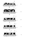
- FIG. 1 It is a schematic process drawing which shows an example of the manufacturing method of the three-dimensional semiconductor integrated element device using the filler for semiconductor element three-dimensional mounting of this invention. It is a schematic process drawing (continuation of FIG. 1) which shows an example of the manufacturing method of the three-dimensional semiconductor integrated element device using the filler for semiconductor element three-dimensional mounting of this invention.
- the filler for semiconductor element three-dimensional mounting according to the present invention (hereinafter sometimes simply referred to as “filler”) is used in the lateral direction when a plurality of semiconductor elements are stacked and integrated to manufacture a three-dimensional semiconductor integrated element device. Is a filler (gap filling material) that fills the gaps between adjacent semiconductor elements. The filler is polished or ground from the surface side of the semiconductor element in a state where the gap between the semiconductor elements is filled, and is flattened.
- FIG. 1 and 2 are schematic process diagrams showing an example of a method for manufacturing a three-dimensional semiconductor integrated device (three-dimensional semiconductor integrated circuit device) using the semiconductor element three-dimensional mounting filler of the present invention.
- a three-dimensional semiconductor integrated device is manufactured as follows.
- A A first base wafer 30 in which a semiconductor element 20 is stacked on a silicon wafer 1 including a circuit formation region is prepared.
- B A gap between adjacent semiconductor elements 20 is filled with the semiconductor element three-dimensional mounting filler 2 of the present invention (a curable composition for semiconductor element three-dimensional mounting described later is poured into the gap). Harden)
- C The surface of the filler 2 is polished and / or ground to be flattened and thinned.
- D to (e)
- a through hole 3 is formed in the semiconductor element 20 or in the semiconductor element three-dimensional mounting filler 2, and a through electrode 4 is formed therein to manufacture a semiconductor wafer 40.
- Such operations are repeated a desired number of times and dicing is performed at a desired position to obtain a three-dimensional semiconductor integrated device (three-dimensional semiconductor integrated circuit device).
- the thickness of the filler 2 is, for example, 10 to 30 ⁇ m by polishing and / or grinding in the step (c).
- the filler is polished or ground from the surface side of the element in a state where the gap between the elements adjacent in the lateral direction is filled with the filler, the element surface side is flattened. Therefore, a low-profile three-dimensional semiconductor integrated device (three-dimensional semiconductor integrated circuit device) in which the device itself is thinned can be efficiently manufactured. At that time, neither cracks nor bubbles are generated.
- the semiconductor element 20 is an element using a semiconductor, and may be a MEMS or an image sensor, for example. Moreover, the semiconductor element 20 ′ to be stacked may be the same size as the semiconductor element 20 or may have different sizes (vertical, horizontal, and height).
- the silicon wafer 1 including the circuit formation region may be a MEMS or an image sensor.
- the filler 2 is preferably a cured product of a curable composition containing at least an epoxy compound having a bisphenol skeleton and a cationic polymerization initiator.
- the curable composition for three-dimensional mounting of a semiconductor element of the present invention contains at least an epoxy compound having a bisphenol skeleton and a cationic polymerization initiator, It is liquid at 25 ° C.
- the curable composition of this invention can be used for formation of the said filler for semiconductor element three-dimensional mounting. That is, the filler is formed by injecting the curable composition of the present invention into a gap between adjacent elements in the lateral direction and curing.
- the curable composition of the present invention contains at least an epoxy compound having a bisphenol skeleton as a curable compound (in particular, a cationic curable compound).
- a curable compound in particular, a cationic curable compound.
- an epoxy compound having a bisphenol skeleton is used as the curable compound, cracks do not occur at the time of curing, and cracks and chips do not occur even after polishing after curing, and clogging of the polishing disk does not occur.
- the conventional element laminating adhesive is diverted to the above-mentioned gap filling agent, cracks or chips occur during polishing or after curing, or clogging of the polishing disk occurs.
- the cured product is too hard, or curing shrinkage occurs, and the cured product is likely to crack.
- These epoxy compounds may have structural units other than the structural units derived from bisphenol and epichlorohydrin in the molecule.
- epoxy compound having a bisphenol skeleton include compounds represented by the following formulas (1), (2), and (3).
- r represents a number from 0 to 8.
- r is preferably in the range of 0.01 to 3, particularly preferably in the range of 1 to 2.
- the epoxy equivalent of the epoxy compound having a bisphenol skeleton is, for example, 155 to 800 g / eq, preferably 155 to 500 g / eq, particularly preferably 160 to 200 g / eq, and most preferably 160 to 190 g / eq.
- the epoxy compound having a bisphenol skeleton is preferably a compound that exhibits a liquid state at room temperature (25 ° C.), but even if it is a solid, other liquid compounds (at 25 ° C.) that dissolve the epoxy compound having a bisphenol skeleton (for example, In combination with other epoxy compounds, etc., the entire curable compound may be liquid (25 ° C.).
- the curable composition of the present invention may contain an epoxy compound other than an epoxy compound having a bisphenol skeleton.
- alicyclic ring examples include monocyclic alicyclic rings such as cyclopentane ring, cyclohexane ring, cyclooctane ring, and cyclododecane ring (3 to 15-membered, preferably about 5 to 6-membered cycloalkane ring); decalin ring ( Perhydronaphthalene ring), perhydroindene ring (bicyclo [4.3.0] nonane ring), perhydroanthracene ring, perhydrofluorene ring, perhydrophenanthrene ring, perhydroacenaphthene ring, perhydrophenalene ring, Norbornane ring (bicyclo [2.2.1] heptane ring), isobornane ring, adamantane ring, bicyclo [3.3.0] octane ring, tricyclo [5.2.1.0 2,6 ] decane ring, tricyclo
- Examples of the alicyclic epoxy group include an epoxycyclopentyl group, a 3,4-epoxycyclohexyl group, and a 3,4-epoxytricyclo [5.2.1.0 2,6 ] decane 8- (or 9) yl.
- a substituent such as an alkyl group for example, an alkyl group having 1 to 6 carbon atoms such as a methyl group
- Examples of the alicyclic epoxy compound include a compound represented by the following formula (4) (a compound in which two alicyclic epoxy groups are bonded by a single bond or via a linking group).
- Y 1 represents a single bond or a linking group.
- the linking group include a divalent hydrocarbon group, a carbonyl group (—CO—), an ether bond (—O—), an ester bond (—COO—), an amide bond (—CONH—), a carbonate bond (— OCOO-) and a group in which a plurality of these are bonded.
- divalent hydrocarbon group examples include linear or branched alkylene groups such as methylene, ethylidene, isopropylidene, ethylene, propylene, trimethylene, and tetramethylene groups (particularly, C 1-6 alkylene groups); 2-valent such as 2-cyclopentylene, 1,3-cyclopentylene, cyclopentylidene, 1,2-cyclohexylene, 1,3-cyclohexylene, 1,4-cyclohexylene, cyclohexylidene group, etc. And an alicyclic hydrocarbon group (particularly a divalent cycloalkylene group); and a group in which a plurality of these are bonded.
- alkylene groups such as methylene, ethylidene, isopropylidene, ethylene, propylene, trimethylene, and tetramethylene groups (particularly, C 1-6 alkylene groups)
- 2-valent such as 2-cyclopentylene, 1,3-cyclopenty
- Representative compounds included in the compound represented by the formula (4) include (3,4,3 ′, 4′-diepoxy) bicyclohexyl, bis (3,4-epoxycyclohexylmethyl) ether, 1,2 -Epoxy-1,2-bis (3,4-epoxycyclohexane-1-yl) ethane, 2,2-bis (3,4-epoxycyclohexane-1-yl) propane, 1,2-bis (3,4 -Epoxycyclohexane-1-yl) ethane and the compounds represented by the following formulas (4-1) to (4-6).
- t is an integer of 1 to 30.
- alicyclic epoxy compound examples include a compound having an alicyclic ring and two or more epoxy groups in the molecule, and only one of the two or more epoxy groups is an alicyclic epoxy group.
- this representative compound include limonene diepoxide represented by the following formula (5).
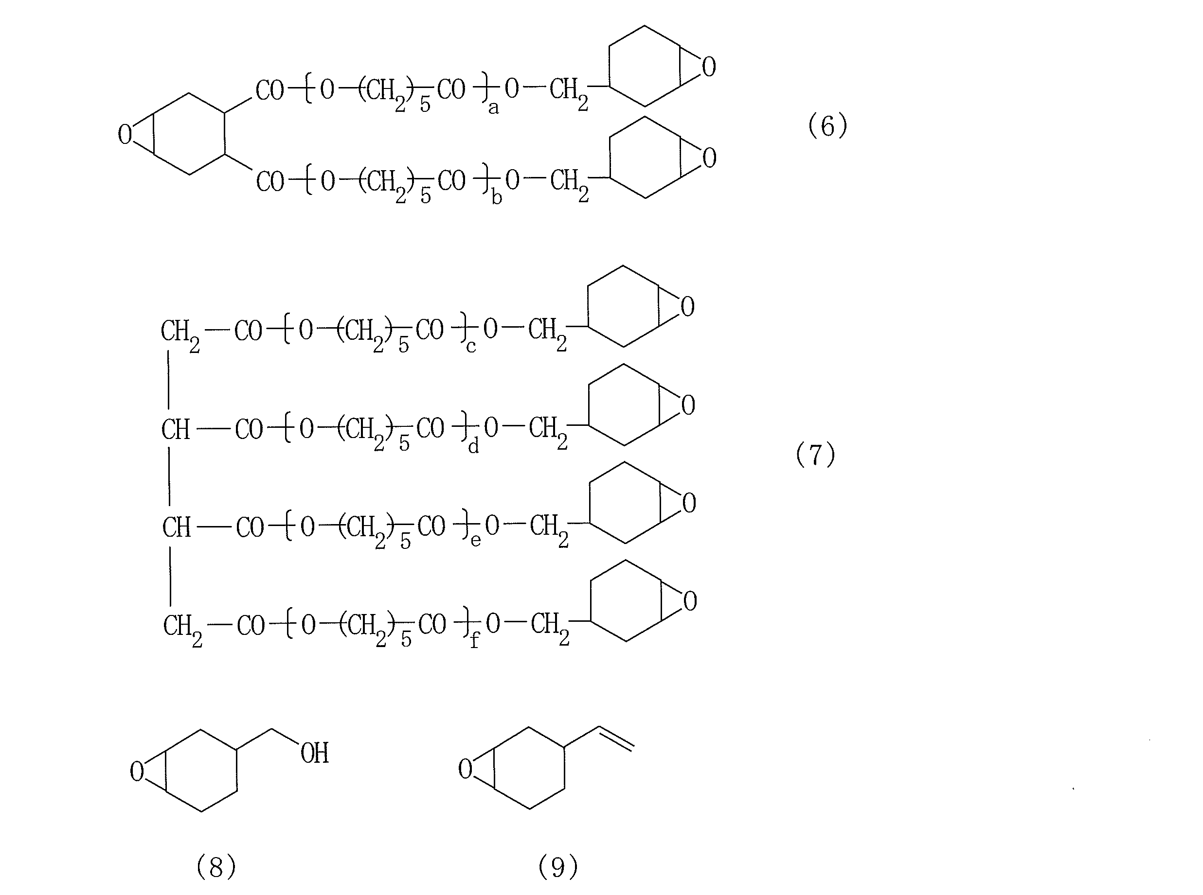
- alicyclic epoxy compound one alicyclic epoxy compound having three or more alicyclic epoxy groups, such as compounds represented by the following formulas (6) to (9), or one alicyclic epoxy group: It is also possible to use an alicyclic epoxy compound having only an epoxy group and no epoxy group.
- a, b, c, d, e, and f are integers from 0 to 30.
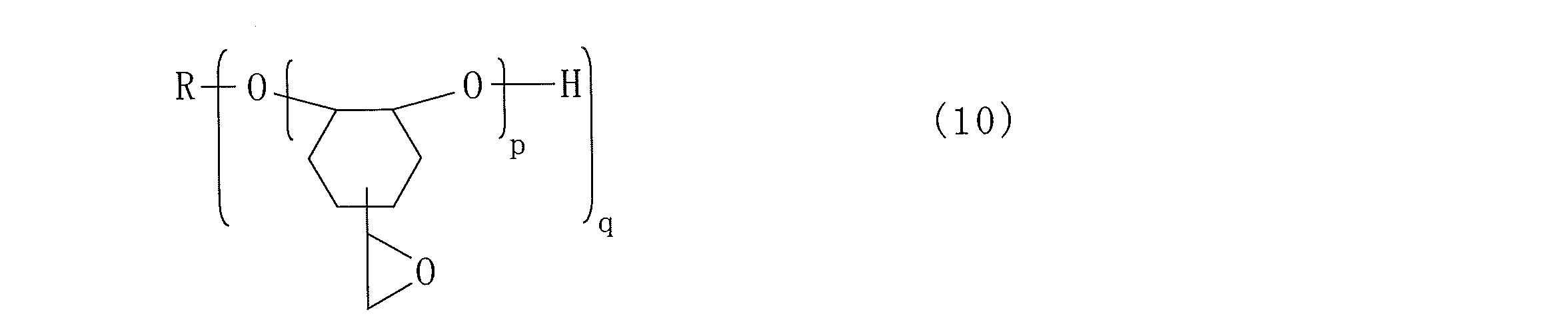
- Examples of the epoxy compound in which an epoxy group is directly bonded to the alicyclic ring with a single bond include a compound represented by the following formula (10).
- R is a group obtained by dividing q OH from a q-valent alcohol [R— (OH) q ], p is an integer of 1 to 30, and q is an integer of 1 to 10. In the groups in q parentheses, p may be the same or different.
- the q-valent alcohol [R- (OH) q] includes monohydric alcohols such as methanol, ethanol, 1-propanol, isopropyl alcohol and 1-butanol; ethylene glycol, 1,2-propanediol, 1,3- Divalent alcohols such as propanediol, 1,4-butanediol, neopentyl glycol, 1,6-hexanediol, diethylene glycol, triethylene glycol, tetraethylene glycol, dipropylene glycol, polypropylene glycol; glycerin, diglycerin, erythritol And trivalent or higher alcohols such as trimethylolethane, trimethylolpropane, pentaerythritol, dipentaerythritol, and sorbitol.
- monohydric alcohols such as methanol, ethanol, 1-propanol, isopropyl alcohol and 1-butanol
- the alcohol may be polyether polyol, polyester polyol, polycarbonate polyol, polyolefin polyol, or the like.
- the alcohol is preferably an aliphatic alcohol having 1 to 10 carbon atoms (particularly an aliphatic polyhydric alcohol such as trimethylolpropane).
- Examples of the glycidyl ether type epoxy compound having an alicyclic ring and a glycidyl ether group include glycidyl ethers of alicyclic alcohols (particularly alicyclic polyhydric alcohols).
- This compound may be a compound in which the aromatic ring of the epoxy compound having the bisphenol skeleton [for example, the compound represented by the formula (1), (2), (3)] is nuclear hydrogenated.
- Examples of the other epoxy compounds include glycidyl ethers of the above-described q-valent alcohol [R— (OH) q ]; acetic acid, propionic acid, butyric acid, stearic acid, adipic acid, sebacic acid, maleic acid, itaconic acid, and the like.
- Glycidyl esters of mono- or polyvalent carboxylic acids epoxidized products of oils and fats having double bonds such as epoxidized linseed oil, epoxidized soybean oil, and epoxidized castor oil; polyolefins such as epoxidized polybutadiene (including polyalkadienes) Examples include epoxidized products.
- an alicyclic epoxy compound is preferable.
- the heat resistance of the cured product (filler 2) can be improved, and the hardness of the cured product changes in a high temperature environment. Can be suppressed.
- the curable composition of the present invention may contain other curable compounds in addition to the epoxy compound, but the total curable compound (particularly, all cationic curable compounds) contained in the curable composition of the present invention.
- the proportion of the epoxy compound is, for example, 50% by weight or more, preferably 70% by weight or more, particularly preferably 85% by weight or more, and most preferably 90% by weight or more.
- the upper limit of the proportion of the epoxy compound is 100% by weight. is there.
- the content of the curable compound in the curable composition of the present invention is, for example, 30 to 99.99% by weight, preferably 50 to 99.9% by weight, and more preferably Is 60 to 99.5% by weight.
- the content of the epoxy compound in the curable composition of the present invention (when two or more types are contained, the total amount thereof) is, for example, 30 to 99.99% by weight, preferably 50 to 99.9% by weight, and more preferably 60 to 99.5% by weight.
- the proportion of the epoxy compound having a bisphenol skeleton in the total curable compound in the curable composition of the present invention is, for example, 30% by weight or more, preferably 40% by weight or more, more preferably 50% by weight or more, and particularly preferably 70%. % By weight or more.
- the ratio of the epoxy compound having a bisphenol skeleton in the total epoxy compound in the curable composition of the present invention is, for example, 30% by weight or more, preferably 40% by weight or more, more preferably 50% by weight or more, and particularly preferably 70% by weight. % Or more.
- the ratio of the total amount of the epoxy compound having a bisphenol skeleton and the alicyclic epoxy compound in the total curable compound in the curable composition of the present invention is, for example, 50% by weight or more, preferably 70% by weight or more, more preferably 90% by weight or more.
- the ratio of the total amount of the epoxy compound having a bisphenol skeleton and the alicyclic epoxy compound in the total epoxy compound in the curable composition of the present invention is, for example, 50% by weight or more, preferably 70% by weight or more, and more preferably 90%. % By weight or more.
- the ratio of the content of the epoxy compound having a bisphenol skeleton and the alicyclic epoxy compound in the curable composition of the present invention is, for example, 55:45 to 99: 1, preferably 60: 40-95: 5, preferably 70: 30-90: 10.
- the curable composition of the present invention contains a cationic polymerization initiator (curing catalyst).
- the cationic polymerization initiator is a compound that releases a substance that initiates cationic polymerization by light irradiation or heating.
- examples of cationic polymerization initiators that generate cationic species by light irradiation include triarylsulfonium salts (for example, hexafluoroantimonate salts, pentafluorohydroxyantimonate salts, hexafluorophosphate salts, hexafluorophosphate salts, Fluoroarsenate salt), etc., and trade names “CPI-100P”, “CPI-101A”, “LW-S1” (manufactured by San Apro Co., Ltd.), trade names “CD-1010”, “ Commercial products such as “CD-1011”, “CD-1012” (manufactured by Sartomer, USA), trade name “Irgacure 264” (manufactured by BASF), and trade name “CIT-1682” (manufactured by Nippon Soda Co., Ltd.) It can be preferably used.
- triarylsulfonium salts for example, hexafluoroanti
- examples of the cationic polymerization initiator that generates a cationic species by heating include aryldiazonium salts, aryliodonium salts, arylsulfonium salts, and allene-ion complexes.
- a compound of a chelate compound of a metal such as aluminum or titanium and acetoacetic acid or diketone and a silanol such as triphenylsilanol, or a chelate compound of a metal such as aluminum or titanium and acetoacetic acid or diketone and bisphenol S A compound with any of the above phenols may also be used.
- the curable composition of the present invention contains a cationic polymerization initiator, it can be cationically cured by heat or light to form the filler.
- the blending amount of the cationic polymerization initiator is not particularly limited, but is 0.01 with respect to 100 parts by weight of the total curable compound (preferably the total cationic curable compound, particularly preferably the total epoxy compound) in the curable composition. Is preferably 15 to 15 parts by weight, more preferably 0.05 to 10 parts by weight, still more preferably 0.1 to 8 parts by weight, particularly preferably 0.1 to 5 parts by weight, and most preferably 0.1 to 3 parts by weight. It is.
- blending in the said range favorable hardened
- the curable composition of the present invention may contain an inorganic and / or organic filler.
- an inorganic and / or organic filler By containing an inorganic and / or organic filler, thermal expansion of the cured product (filler 2) can be suppressed and heat resistance can be improved.
- examples of the inorganic filler include silica, alumina, magnesia, titania, antimony oxide, talc, clay, montmorillonite, hydrotalcite, synthetic mica, calcium carbonate, aluminum hydroxide, magnesium hydroxide and the like. These can be used individually by 1 type or in combination of 2 or more types. Of these, silica (particularly spherical silica) and alumina are preferable.
- the average particle diameter of the inorganic filler is, for example, 0.05 to 1 ⁇ m, preferably 0.1 to 1 ⁇ m.
- the amount of the inorganic filler is, for example, 70 parts by weight or less (for example, based on 100 parts by weight of the total curable compound (preferably the total cationic curable compound, particularly preferably the total epoxy compound) in the curable composition of the present invention (for example, 0.1 to 70 parts by weight), preferably 50 parts by weight or less (eg 1 to 50 parts by weight), more preferably 40 parts by weight or less (eg 5 to 40 parts by weight).
- organic filler examples include polyimide, polyether ether ketone, aramid, and cellulose. These can be used individually by 1 type or in combination of 2 or more types. Among these, polyimide (particularly spherical polyimide) and polyetheretherketone (particularly spherical polyetheretherketone) are preferable.
- the blending amount of the organic filler is, for example, 70 parts by weight or less (for example, less than 70 parts by weight with respect to 100 parts by weight of the total curable compound (preferably the total cationic curable compound, particularly preferably the total epoxy compound) in the curable composition of the present invention.
- 70 parts by weight or less for example, less than 70 parts by weight with respect to 100 parts by weight of the total curable compound (preferably the total cationic curable compound, particularly preferably the total epoxy compound) in the curable composition of the present invention.
- 0.1 to 70 parts by weight preferably 50 parts by weight or less (eg 1 to 50 parts by weight), more preferably 40 parts by weight or less (eg 5 to 40 parts by weight).
- the curable composition of the present invention may contain a silane coupling agent.
- a silane coupling agent By containing the silane coupling agent, the adhesion of the cured product (filler 2) to the silicon wafer can be improved.
- silane coupling agent examples include 3-trimethoxysilylpropyl (meth) acrylate, 3-triethoxysilylpropyl (meth) acrylate, 3-dimethoxymethylsilylpropyl (meth) acrylate, 3-diethoxymethylsilylpropyl ( And (meth) acrylate.
- a silane coupling agent whose functional group is a (meth) acryloyloxy group a small amount of a radical polymerization initiator may be added.
- Silane coupling agents whose functional groups are epoxy groups [2- (3,4-epoxycyclohexyl) ethyltrimethoxysilane, 3-glycidoxypropylmethyldimethoxysilane, 3-glycidoxypropyltrimethoxysilane, 3 -Glycidoxypropylmethyldiethoxysilane, 3-glycidoxypropyltriethoxysilane, etc.] can also be used, and such coupling agents belong to the other epoxy compounds.
- the amount of the silane coupling agent is, for example, 10 parts by weight or less with respect to 100 parts by weight of the total curable compound (preferably the total cationic curable compound, particularly preferably the total epoxy compound) in the curable composition of the present invention.
- the total curable compound preferably the total cationic curable compound, particularly preferably the total epoxy compound
- the amount of the silane coupling agent is, for example, 10 parts by weight or less with respect to 100 parts by weight of the total curable compound (preferably the total cationic curable compound, particularly preferably the total epoxy compound) in the curable composition of the present invention.
- 0.1 to 10 parts by weight preferably 5 parts by weight or less (for example, 0.2 to 5 parts by weight), and more preferably 3 parts by weight or less (for example, 0.3 to 3 parts by weight).
- various additives for example, silicone-based and fluorine-based antifoaming agents, leveling agents, surfactants, organic compounds, and the like
- the blending amount of the various additives is, for example, 5% by weight or less with respect to the entire curable composition.
- the curable composition of the present invention may contain a solvent, but if the amount of the solvent is too large, bubbles may be formed in the cured product. , Preferably 10% by weight or less, particularly preferably 5% by weight or less, most preferably 1% by weight or less.
- the total content of the epoxy compound, the cationic polymerization initiator, the inorganic filler, the organic filler, and the silane coupling agent is, for example, 80% by weight or more, preferably with respect to the entire curable composition. Is 90% by weight or more, particularly preferably 95% by weight or more, and most preferably 99% by weight or more.
- the curable composition of the present invention exhibits a liquid state at 25 ° C., and its viscosity (25 ° C.) is, for example, 10 to 100,000 mPa ⁇ s, preferably 100 to 10000 mPa ⁇ s, particularly preferably 500 to 10000 mPa ⁇ s, most preferably. 500 to 3000 mPa ⁇ s.
- the curable composition of the present invention is preferably in the form of a paste having fluidity at room temperature. When the viscosity of the curable composition of the present invention is too large, bubbles are difficult to escape, and workability, handleability, and the like are liable to decrease.
- the viscosity can be measured using a B-type viscometer or a D-type viscometer.
- the curable composition of the present invention may be either a one-component type or a two-component type.
- the curable composition of the present invention is a mixture of an epoxy compound having a bisphenol skeleton and a cationic polymerization initiator, and if necessary, an alicyclic epoxy compound, an inorganic or organic filler, a silane coupling agent, and other additives. Can be prepared.
- a general-purpose mixer or kneader can be used for the stirring and mixing.
- the curable composition for three-dimensional mounting of a semiconductor element thus prepared is injected into a gap between adjacent semiconductor elements in the lateral direction when manufacturing a three-dimensional semiconductor integrated element device, and is cured (photocured or cured) under predetermined conditions. It is cured by heating) and functions as the filler 2.
- examples of the active energy ray (light) to be irradiated include ultraviolet rays and electron beams, among which ultraviolet rays can be preferably used.
- the wavelength of the ultraviolet light can be appropriately selected according to the type of the cationic polymerization initiator.
- the irradiation conditions of the active energy rays can be appropriately selected according to the type and thickness of the compounded epoxy compound, the type and amount of the cationic polymerization initiator, for example, when using ultraviolet rays,
- the irradiation amount (dose) is preferably 10 to 30000 mJ / cm 2 , particularly preferably 50 to 25000 mJ / cm 2 .
- Examples of the ultraviolet irradiation source include a high pressure mercury lamp, an ultrahigh pressure mercury lamp, a xenon lamp, a carbon arc, a metal halide lamp, sunlight, and an LED lamp.
- the curable composition of the present invention may be further heated as necessary (post-cure).
- post-cure effects such as reduction of unreacted substances in the cured product, improvement of the degree of cure of the cured product, and relaxation of strain can be obtained.
- cured material may be acquired.
- the above heating can usually be performed at a temperature of 100 to 200 ° C. for 1 to 300 minutes.
- the curing temperature when the curable composition of the present invention is heat-cured is, for example, about 45 to 200 ° C., and the curing time is, for example, about 1 to 60 minutes. Heat curing can also be performed in multiple stages.
- the curable composition when the curable composition is injected into the gap between the adjacent semiconductor elements, the fluidity of the curable composition is increased by heat and gathers in the center (the wettability with the silicon wafer is increased). Since the in-plane film thickness distribution may not be constant, photocuring is more preferable.
- the cured product obtained by curing the curable composition of the present invention is excellent in toughness and does not generate cracks or chips even when subjected to polishing treatment.
- the cured product obtained by curing the curable composition of the present invention is excellent in heat resistance, and the glass transition temperature (Tg: ° C.) is, for example, 30 ° C. or higher, preferably 50 ° C. or higher, particularly preferably 80 ° C. or higher. It is.
- the thermal expansion coefficient (ppm / K) is, for example, 150 or less, preferably 100 or less.
- Example 1 100 parts by weight of a bisphenol F type epoxy resin and 2 parts by weight of a cationic polymerization initiator “CPI-100P” are stirred and mixed with a rotation / revolution mixer (trade name “Awatori Netaro”, manufactured by Shinky Corporation). A curable composition was obtained.
- an 8-inch silicon wafer was prepared by cutting a concave-convex shape resembling a chip (simulated COW substrate: wafer thickness 725 ⁇ m, chip portion 9 mm ⁇ 9 mm ⁇ 0.2 mm thickness, groove portion 2 mm) Width x 0.1 mm thickness). That is, grooves having a width of 2 mm and a depth of 0.2 mm were formed on the surface of an 8-inch silicon wafer at intervals of 10 mm in the vertical and horizontal directions, respectively.
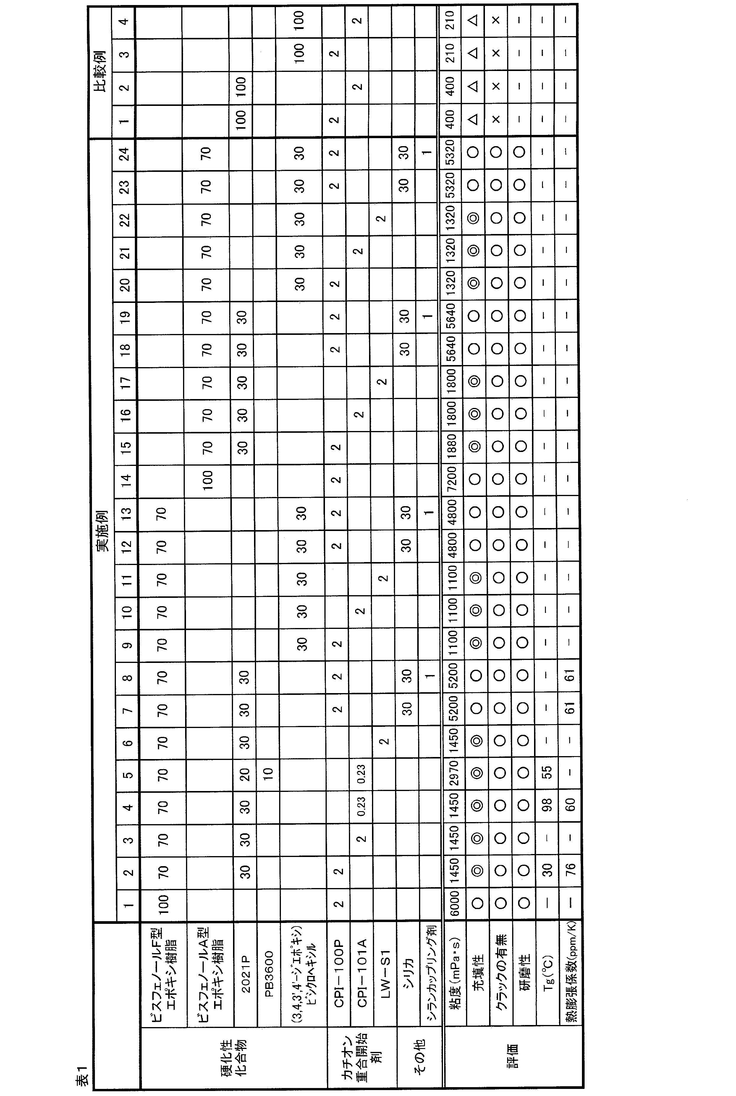
- a coating film is formed by applying the curable composition for a filler obtained in the above-described Examples and Comparative Examples to the surface of the simulated COW substrate using a squeegee (J Squeegee manufactured by Neurong Seimitsu Kogyo Co., Ltd.). Formed. The obtained coating film was visually observed, and the filling property was evaluated according to the following criteria. ⁇ Evaluation criteria> The tip part and groove part are filled, and no bubbles remain in the groove part: ⁇ Chip part and groove part are filled, but bubbles remain in the groove part: ⁇ Only the groove part is filled: ⁇
- the coating film was irradiated with UV light (UV-A) at 3600 mJ / cm 2 (photocuring) with a UV irradiation machine (trade name “UVC-02516S1AA02” manufactured by USHIO INC.), And then a hot plate was used. And heated at 120 ° C. for 10 minutes (post cure) to form a filler. About the obtained filler, the presence or absence of the crack was confirmed visually and with the optical microscope, and the following reference
- polishing machine For samples without cracks, using a polishing machine (Musashino Electronics Co., Ltd., trade name “MA-200D”) and a polishing machine (Mitsui Grinding Wheel Co., Ltd., trade name “CBN DIA # 400”), The polishing test was performed under the conditions of a rotation speed of 100 rpm, a polishing time of 10 minutes, and a weight of 500 g. Since the cracks were confirmed in the fillers obtained in Comparative Examples 1 to 4, no polishing test was performed. After polishing, the presence or absence of cracks or chips in the filler or silicon wafer and the presence or absence of clogging of the polishing disk were confirmed visually and with an optical microscope, and the polishing property was evaluated according to the following criteria.
- the filler or silicon wafer has cracks or chips and / or the clogging of the polishing machine: ⁇
- thermomechanical analyzer (trade name “EXSTAR TMA / SS7100”, manufactured by SII Nano Technology Co., Ltd.).
- CPI-100P diphenyl-4- (phenylthio) phenylsulfonium hexafluorophosphate, trade name “CPI-100P”, manufactured by San Apro, Inc.
- CPI-101A diphenyl-4- (phenylthio) phenylsulfonium hexafluoroantimonate, trade name “CPI -101A ", San Apro LW-S1: sulfonium compound, trade name” LW-S1 ", San Apro ⁇ Others>
- Silica Trade name “SC4050-SEJ”, average particle size 1 ⁇ m, manufactured by Admatechs, Inc.
- Silane coupling agent 3-trimethoxysilylpropyl acrylate
- the filler is polished from the surface side of the semiconductor element with the gap between the thinned semiconductor elements adjacent in the lateral direction filled with the filler.
Landscapes
- Chemical & Material Sciences (AREA)
- Health & Medical Sciences (AREA)
- Chemical Kinetics & Catalysis (AREA)
- Medicinal Chemistry (AREA)
- Polymers & Plastics (AREA)
- Organic Chemistry (AREA)
- Epoxy Resins (AREA)
- Compositions Of Macromolecular Compounds (AREA)
- Structures Or Materials For Encapsulating Or Coating Semiconductor Devices Or Solid State Devices (AREA)
Abstract
Description
[1] 複数の半導体素子を積層し集積して三次元半導体集積素子装置を製造する際に、横方向に隣接する半導体素子間の隙間を埋める充填材であって、該充填材は、半導体素子間の隙間を埋めた状態で半導体素子の表面側から研磨及び/又は研削され、平坦化される部材であることを特徴とする半導体素子三次元実装用充填材。
[2] 前記充填材が、ビスフェノール骨格を有するエポキシ化合物とカチオン重合開始剤とを少なくとも含有する硬化性組成物の硬化物である[1]記載の半導体素子三次元実装用充填材。
[3] 前記硬化性組成物の硬化物のガラス転移温度が30℃以上である[2]記載の半導体素子三次元実装用充填材。
[4] 前記硬化性組成物の硬化物の熱膨張係数(ppm/K)が150以下である[2]又は[3]記載の半導体素子三次元実装用充填材。
[5] [1]~[4]の何れか1つに記載の半導体素子三次元実装用充填材の形成に用いる硬化性組成物であって、ビスフェノール骨格を有するエポキシ化合物を含む硬化性化合物とカチオン重合開始剤とを少なくとも含有し、25℃において液状である半導体素子三次元実装用硬化性組成物。
[6] ビスフェノール骨格を有するエポキシ化合物が、式(1)~(3)で表される化合物から選択される少なくとも1種である[5]に記載の半導体素子三次元実装用硬化性組成物。
[7] ビスフェノール骨格を有するエポキシ化合物のエポキシ当量が155~800g/eqである[5]又は[6]に記載の半導体素子三次元実装用硬化性組成物。
[8] さらに、脂環式エポキシ化合物を含有する[5]~[7]の何れか1つに記載の半導体素子三次元実装用硬化性組成物。
[9] 脂環式エポキシ化合物が、式(4)で表される化合物である[8]に記載の半導体素子三次元実装用硬化性組成物。
[10] 脂環式エポキシ化合物が、式(4-1)~(4-6)で表される化合物から選択される少なくとも1種である[8]に記載の半導体素子三次元実装用硬化性組成物。
[11] 硬化性組成物全量(100重量%)中に硬化性化合物を30~99.99重量%含有する[5]~[10]の何れか1つに記載の半導体素子三次元実装用硬化性組成物。
[12] 硬化性組成物に含まれる全硬化性化合物に占めるビスフェノール骨格を有するエポキシ化合物の割合が30重量%以上である[5]~[11]の何れか1つに記載の半導体素子三次元実装用硬化性組成物。
[13] 硬化性組成物に含まれる全硬化性化合物に占めるビスフェノール骨格を有するエポキシ化合物と脂環式エポキシ化合物の総量の割合が50重量%以上である[5]~[12]の何れか1つに記載の半導体素子三次元実装用硬化性組成物。
[14] 硬化性組成物に含まれるビスフェノール骨格を有するエポキシ化合物と脂環式エポキシ化合物の含有量の比(前者:後者(重量部))が55:45~99:1である[8]~[13]の何れか1つに記載の半導体素子三次元実装用硬化性組成物。
[15] 硬化性組成物に含まれる硬化性化合物(好ましくはカチオン硬化性化合物、特に好ましくはエポキシ化合物)100重量部に対して、カチオン重合開始剤を0.01~15重量部含有する[5]~[14]の何れか1つに記載の半導体素子三次元実装用硬化性組成物。
[16] さらに、平均粒子径0.05~1μmの無機及び/又は有機フィラーを含有する[5]~[15]の何れか1つに記載の半導体素子三次元実装用硬化性組成物。
[17] 無機及び/又は有機フィラーを硬化性化合物(好ましくはカチオン硬化性化合物、特に好ましくはエポキシ化合物)100重量部に対して、0.1~70重量部含有する[16]に記載の半導体素子三次元実装用硬化性組成物。
[18] さらに、シランカップリング剤を含有する[5]~[17]の何れか1つに記載の半導体素子三次元実装用硬化性組成物。
[19] シランカップリング剤を硬化性化合物(好ましくはカチオン硬化性化合物、特に好ましくはエポキシ化合物)100重量部に対して、0.1~10重量部含有する[18]に記載の半導体素子三次元実装用硬化性組成物。
[20] エポキシ化合物、カチオン重合開始剤、無機フィラー、有機フィラー、及びシランカップリング剤の含有量の和が、硬化性組成物全量の80重量%以上である[18]又は[19]に記載の半導体素子三次元実装用硬化性組成物。
[21] 硬化性組成物の粘度(25℃における)が10~100000mPa・sである[5]~[20]の何れか1つに記載の半導体素子三次元実装用硬化性組成物。
[22] [5]~[21]の何れか1つに記載の半導体素子三次元実装用硬化性組成物の硬化物によって半導体素子間を充填し、半導体素子間を充填した状態で半導体素子の表面側から研磨及び/又は研削して平坦化する工程を含む三次元半導体集積素子装置の製造方法。
[23] [22]に記載の三次元半導体集積素子装置の製造方法により得られる三次元半導体集積素子装置。
本発明の半導体素子三次元実装用充填材(以下、単に「充填材」と称する場合がある)は、複数の半導体素子を積層し集積して三次元半導体集積素子装置を製造するに際し、横方向に隣接する半導体素子間の隙間を埋める充填材(隙間埋め材)である。この充填材は、半導体素子間の隙間を埋めた状態で半導体素子の表面側から研磨又は研削され、平坦化される。
(b)隣接する半導体素子20間の隙間を、本発明の半導体素子三次元実装用充填材2で埋めた状態にする(前記隙間に後述する半導体素子三次元実装用硬化性組成物を流し込んで硬化させる)
(c)前記充填材2の表面を研磨及び/又は研削して、平坦化・薄化する。
(d)~(e)半導体素子20内部または半導体素子三次元実装用充填材2に貫通孔3を作製し、そこに貫通電極4を形成して半導体ウェハ40を作製する。
本発明の半導体素子三次元実装用硬化性組成物(以下、「本発明の硬化性組成物」と称する場合がある)は、ビスフェノール骨格を有するエポキシ化合物とカチオン重合開始剤とを少なくとも含有し、25℃において液状である。本発明の硬化性組成物は、前記半導体素子三次元実装用充填材の形成に用いることができる。すなわち、本発明の硬化性組成物を横方向に隣接する素子間の隙間に注入し、硬化させることにより前記充填材が形成される。
本発明の硬化性組成物は硬化性化合物(特に、カチオン硬化性化合物)としてビスフェノール骨格を有するエポキシ化合物を少なくとも含有する。硬化性化合物としてビスフェノール骨格を有するエポキシ化合物を用いると、硬化時にクラックが入らず、また、硬化後研磨してもクラックや欠けが生じず、研磨盤の目詰まりも起こさない。なお、従来の素子積層用接着剤を上記の隙間埋め剤に転用した場合には、硬化時や硬化後に研磨する際にクラックや欠けが生じたり、研磨盤の目詰まりを起こす。また、硬化性化合物として脂環式エポキシ化合物のみを用いた場合には、硬化物が硬すぎたり、硬化収縮が生じたりして、硬化物にクラックが生じやすい。




本発明の硬化性組成物はカチオン重合開始剤(硬化触媒)を含有する。カチオン重合開始剤は光照射又は加熱によりカチオン重合を開始させる物質を放出する化合物である。
本発明の硬化性組成物は無機及び/又は有機フィラーを含有していてもよい。無機及び/又は有機フィラーを含有することにより、硬化物(充填材2)の熱膨張を抑制し、耐熱性を向上することができる。
ビスフェノールF型エポキシ樹脂100重量部、及びカチオン重合開始剤「CPI-100P」2重量部を自転・公転ミキサー(シンキー社製、商品名「あわとり練太郎」)で撹拌混合し、充填材用の硬化性組成物を得た。
表1に記載のとおりに処方を変更した以外は実施例1と同様にして充填材用の硬化性組成物を得た。
塗布基板として、8インチシリコンウェハにチップに見立てた凹凸形状を切削加工にて作製したものを準備した(模擬COW基板:ウェハ厚み725μm、チップ部9mm×9mm×0.2mm厚、溝部2mm幅×0.1mm厚)。すなわち、8インチシリコンウェハの表面に、縦方向及び横方向にそれぞれ10mm間隔で幅2mm×深さ0.2mmの溝を作製した。
この模擬COW基板の表面に上記実施例及び比較例で得られた充填材用の硬化性組成物をスキージ(ニューロング精密工業(株)製のJスキージ)を使用して塗布して塗膜を形成した。
得られた塗膜を目視で観察し、充填性について下記基準で評価した。
<評価基準>
チップ部、溝部ともに充填され、溝部に気泡が全く残存していないもの:◎
チップ部、溝部ともに充填されたが、溝部に気泡が残存するもの:〇
溝部のみに充填されたもの:△
得られた充填材について、クラックの有無を目視と光学顕微鏡で確認し、下記基準で評価した。
<評価基準>
クラックの無いもの:○
クラックのあるもの:×
研磨後、充填材やシリコンウェハにおけるクラックや欠けの有無、及び研磨盤の目詰まりの有無を目視と光学顕微鏡で確認し、下記基準により研磨性を評価した。
<評価基準>
充填材やシリコンウェハにクラックや欠けがなく、研磨盤の目詰まりがないもの:○
充填材やシリコンウェハにクラックや欠けがあるもの及び/又は研磨盤の目詰まりがあるもの:×
<硬化性化合物>
ビスフェノールF型エポキシ樹脂:ビスフェノールF・エピクロルヒドリンのジグリシジルエーテル、エポキシ当量:168g/eq、商品名「RE-303S」、日本化薬(株)製
ビスフェノールA型エポキシ樹脂:ビスフェノールA・エピクロルヒドリンのジグリシジルエーテル、エポキシ当量:185g/eq、商品名「RE-410S」、日本化薬(株)製
2021P:3,4-エポキシシクロヘキシルメチル(3,4-エポキシ)シクロヘキサンカルボキシレート、商品名「セロキサイド2021P」、(株)ダイセル製
PB3600:エポキシ化ポリブタジエン、商品名「エポリード PB3600」、(株)ダイセル製
<カチオン重合開始剤>
CPI-100P:ジフェニル-4-(フェニルチオ)フェニルスルホニウムヘキサフルオロホスフェート、商品名「CPI-100P」、サンアプロ社製
CPI-101A:ジフェニル-4-(フェニルチオ)フェニルスルホニウムヘキサフルオロアンチモネート、商品名「CPI-101A」、サンアプロ社製
LW-S1:スルホニウム化合物、商品名「LW-S1」、サンアプロ社製
<その他>
シリカ:商品名「SC4050-SEJ」、平均粒子径1μm、アドマテックス社製
シランカップリング剤:3-トリメトキシシリルプロピルアクリレート
2 半導体素子三次元実装用充填材
3 貫通孔
4 貫通電極
20、20’ 半導体素子
30 第1のベースウェハ
40 2層の配線層を有する半導体ウェハ
50 3層の配線層を有する半導体ウェハ
Claims (6)
- 複数の半導体素子を積層し集積して三次元半導体集積素子装置を製造する際に、横方向に隣接する半導体素子間の隙間を埋める充填材であって、該充填材は、半導体素子間の隙間を埋めた状態で半導体素子の表面側から研磨及び/又は研削され、平坦化される部材であることを特徴とする半導体素子三次元実装用充填材。
- 前記充填材が、ビスフェノール骨格を有するエポキシ化合物とカチオン重合開始剤とを少なくとも含有する硬化性組成物の硬化物である請求項1記載の半導体素子三次元実装用充填材。
- 請求項1又は2記載の半導体素子三次元実装用充填材の形成に用いる硬化性組成物であって、ビスフェノール骨格を有するエポキシ化合物とカチオン重合開始剤とを少なくとも含有し、25℃において液状である半導体素子三次元実装用硬化性組成物。
- さらに、脂環式エポキシ化合物を含有する請求項3記載の半導体素子三次元実装用硬化性組成物。
- さらに、平均粒子径0.05~1μmの無機及び/又は有機フィラーを含有する請求項3又は4記載の半導体素子三次元実装用硬化性組成物。
- さらに、シランカップリング剤を含有する請求項3~5のいずれか1項に記載の半導体素子三次元実装用硬化性組成物。
Priority Applications (4)
| Application Number | Priority Date | Filing Date | Title |
|---|---|---|---|
| US15/024,910 US10308758B2 (en) | 2013-09-27 | 2014-09-25 | Filling material for three-dimensional mounting of semiconductor element |
| CN201480052924.4A CN105580133A (zh) | 2013-09-27 | 2014-09-25 | 半导体元件三维安装用填充材料 |
| KR1020167007754A KR102225809B1 (ko) | 2013-09-27 | 2014-09-25 | 반도체 소자 삼차원 실장용 충전재 |
| JP2015539334A JPWO2015046334A1 (ja) | 2013-09-27 | 2014-09-25 | 半導体素子三次元実装用充填材 |
Applications Claiming Priority (2)
| Application Number | Priority Date | Filing Date | Title |
|---|---|---|---|
| JP2013201591 | 2013-09-27 | ||
| JP2013-201591 | 2013-09-27 |
Publications (1)
| Publication Number | Publication Date |
|---|---|
| WO2015046334A1 true WO2015046334A1 (ja) | 2015-04-02 |
Family
ID=52743468
Family Applications (1)
| Application Number | Title | Priority Date | Filing Date |
|---|---|---|---|
| PCT/JP2014/075433 Ceased WO2015046334A1 (ja) | 2013-09-27 | 2014-09-25 | 半導体素子三次元実装用充填材 |
Country Status (6)
| Country | Link |
|---|---|
| US (1) | US10308758B2 (ja) |
| JP (2) | JPWO2015046334A1 (ja) |
| KR (1) | KR102225809B1 (ja) |
| CN (1) | CN105580133A (ja) |
| TW (1) | TWI613718B (ja) |
| WO (1) | WO2015046334A1 (ja) |
Cited By (2)
| Publication number | Priority date | Publication date | Assignee | Title |
|---|---|---|---|---|
| JP2017155091A (ja) * | 2016-02-29 | 2017-09-07 | 日産化学工業株式会社 | 平坦化膜形成用樹脂組成物 |
| WO2024225232A1 (ja) * | 2023-04-28 | 2024-10-31 | 三井化学株式会社 | 半導体構造体及びその製造方法 |
Families Citing this family (5)
| Publication number | Priority date | Publication date | Assignee | Title |
|---|---|---|---|---|
| JP7281901B2 (ja) * | 2018-12-27 | 2023-05-26 | 東京エレクトロン株式会社 | 基板処理装置、および基板処理方法 |
| KR102670364B1 (ko) * | 2019-03-14 | 2024-05-28 | 삼성전자주식회사 | 반도체 패키지, 반도체 패키지용 버퍼 웨이퍼 및 반도체 패키지 제조 방법 |
| KR102891647B1 (ko) * | 2020-09-08 | 2025-11-27 | 주식회사 엘지화학 | 유기전자소자 봉지용 조성물 및 신뢰성 평가 방법 |
| JP7851168B2 (ja) * | 2022-03-30 | 2026-04-24 | アイカ工業株式会社 | カチオン硬化型エポキシ樹脂組成物 |
| JP2024080246A (ja) * | 2022-12-02 | 2024-06-13 | タツモ株式会社 | 積層デバイスの製造方法 |
Citations (5)
| Publication number | Priority date | Publication date | Assignee | Title |
|---|---|---|---|---|
| JP2012151109A (ja) * | 2010-12-28 | 2012-08-09 | Sekisui Chem Co Ltd | 有機エレクトロルミネッセンス表示素子用封止剤 |
| WO2012133760A1 (ja) * | 2011-03-30 | 2012-10-04 | ボンドテック株式会社 | 電子部品実装方法、電子部品実装システムおよび基板 |
| JP2012227441A (ja) * | 2011-04-21 | 2012-11-15 | Sumitomo Bakelite Co Ltd | 半導体装置の製造方法および半導体装置 |
| JP2013118276A (ja) * | 2011-12-02 | 2013-06-13 | Namics Corp | 半導体装置 |
| JP2013256634A (ja) * | 2012-06-14 | 2013-12-26 | Daicel Corp | 半導体素子3次元実装用充填材 |
Family Cites Families (14)
| Publication number | Priority date | Publication date | Assignee | Title |
|---|---|---|---|---|
| US7831703B2 (en) * | 2004-01-07 | 2010-11-09 | Intellinx Ltd. | Apparatus and method for monitoring and auditing activity of a legacy environment |
| WO2005108487A1 (en) * | 2004-04-22 | 2005-11-17 | Henkel Corporation | Methods for improving the flux compatibility of underfill formulations |
| JP4383274B2 (ja) | 2004-06-30 | 2009-12-16 | Necエレクトロニクス株式会社 | 半導体装置および半導体ウエハの製造方法 |
| JP2006299073A (ja) * | 2005-04-20 | 2006-11-02 | Nagase Chemtex Corp | 光半導体封止用樹脂組成物 |
| JP2007284475A (ja) * | 2006-04-12 | 2007-11-01 | Shin Etsu Chem Co Ltd | 紫外線硬化型エンドシール材 |
| JP2009019077A (ja) * | 2007-07-10 | 2009-01-29 | Kyocera Chemical Corp | 硬化性組成物、表示素子用接着剤及び接着方法 |
| JP2009084310A (ja) * | 2007-09-27 | 2009-04-23 | Nippon Shokubai Co Ltd | 熱・光硬化性樹脂組成物、光学材料及び光学部材 |
| US8501033B2 (en) * | 2009-03-13 | 2013-08-06 | Dsm Ip Assets B.V. | Radiation curable resin composition and rapid three-dimensional imaging process using the same |
| JP5229165B2 (ja) * | 2009-09-02 | 2013-07-03 | 住友ベークライト株式会社 | エポキシ樹脂組成物、透明複合シートおよび表示素子用基板 |
| JP2012001689A (ja) * | 2010-06-21 | 2012-01-05 | Adeka Corp | 光硬化性樹脂組成物 |
| JP2012041422A (ja) * | 2010-08-18 | 2012-03-01 | Sekisui Chem Co Ltd | 硬化性組成物及びそれを用いた光半導体装置 |
| JP2012209453A (ja) | 2011-03-30 | 2012-10-25 | Sumitomo Bakelite Co Ltd | 液状樹脂組成物、半導体パッケージ、および半導体パッケージの製造方法 |
| TWI580701B (zh) | 2011-10-27 | 2017-05-01 | 三菱麗陽股份有限公司 | 乙烯基聚合物粉末、硬化性樹脂組成物及硬化物 |
| JP2013194076A (ja) * | 2012-03-16 | 2013-09-30 | Daicel Corp | 硬化性組成物、及びその硬化物 |
-
2014
- 2014-09-25 US US15/024,910 patent/US10308758B2/en not_active Expired - Fee Related
- 2014-09-25 KR KR1020167007754A patent/KR102225809B1/ko not_active Expired - Fee Related
- 2014-09-25 JP JP2015539334A patent/JPWO2015046334A1/ja active Pending
- 2014-09-25 WO PCT/JP2014/075433 patent/WO2015046334A1/ja not_active Ceased
- 2014-09-25 CN CN201480052924.4A patent/CN105580133A/zh active Pending
- 2014-09-26 TW TW103133471A patent/TWI613718B/zh not_active IP Right Cessation
-
2018
- 2018-08-31 JP JP2018162252A patent/JP6762342B2/ja not_active Expired - Fee Related
Patent Citations (5)
| Publication number | Priority date | Publication date | Assignee | Title |
|---|---|---|---|---|
| JP2012151109A (ja) * | 2010-12-28 | 2012-08-09 | Sekisui Chem Co Ltd | 有機エレクトロルミネッセンス表示素子用封止剤 |
| WO2012133760A1 (ja) * | 2011-03-30 | 2012-10-04 | ボンドテック株式会社 | 電子部品実装方法、電子部品実装システムおよび基板 |
| JP2012227441A (ja) * | 2011-04-21 | 2012-11-15 | Sumitomo Bakelite Co Ltd | 半導体装置の製造方法および半導体装置 |
| JP2013118276A (ja) * | 2011-12-02 | 2013-06-13 | Namics Corp | 半導体装置 |
| JP2013256634A (ja) * | 2012-06-14 | 2013-12-26 | Daicel Corp | 半導体素子3次元実装用充填材 |
Cited By (2)
| Publication number | Priority date | Publication date | Assignee | Title |
|---|---|---|---|---|
| JP2017155091A (ja) * | 2016-02-29 | 2017-09-07 | 日産化学工業株式会社 | 平坦化膜形成用樹脂組成物 |
| WO2024225232A1 (ja) * | 2023-04-28 | 2024-10-31 | 三井化学株式会社 | 半導体構造体及びその製造方法 |
Also Published As
| Publication number | Publication date |
|---|---|
| KR102225809B1 (ko) | 2021-03-11 |
| CN105580133A (zh) | 2016-05-11 |
| JP6762342B2 (ja) | 2020-09-30 |
| US20160237201A1 (en) | 2016-08-18 |
| TW201526095A (zh) | 2015-07-01 |
| JP2018193566A (ja) | 2018-12-06 |
| US10308758B2 (en) | 2019-06-04 |
| KR20160061343A (ko) | 2016-05-31 |
| JPWO2015046334A1 (ja) | 2017-03-09 |
| TWI613718B (zh) | 2018-02-01 |
Similar Documents
| Publication | Publication Date | Title |
|---|---|---|
| JP6762342B2 (ja) | 半導体素子三次元実装用充填材 | |
| JP5918699B2 (ja) | 硬化性エポキシ樹脂組成物及びこれを使用した光半導体装置 | |
| JP6285449B2 (ja) | 感光性樹脂組成物及びその硬化物、並びに光学部品 | |
| JP6279489B2 (ja) | ナノインプリント用光硬化性組成物、及びそれを使用した微細パターン基板の製造方法 | |
| CN105579546A (zh) | 半导体叠层用粘接剂组合物 | |
| CN102985458A (zh) | 固化物的制造方法及固化物 | |
| KR101832537B1 (ko) | 경화성 에폭시 수지 조성물 | |
| WO2014196515A1 (ja) | 硬化性エポキシ樹脂組成物 | |
| JP5964666B2 (ja) | 半導体素子3次元実装用充填材 | |
| JP7128112B2 (ja) | 反射防止材 | |
| JP2015089932A (ja) | 光学的立体造形用樹脂組成物 | |
| JP2002201264A (ja) | 封止樹脂用組成物 | |
| WO2022014552A1 (ja) | 組成物、硬化物及び硬化物の製造方法 | |
| TWI846809B (zh) | 有機el顯示元件用密封劑 | |
| JP2018161862A (ja) | 樹脂成型品の製造方法及び光学部品の製造方法 | |
| JP6072138B2 (ja) | 硬化物の製造方法及び硬化物 | |
| US20240210817A1 (en) | Resin molded article production method and optical component production method | |
| WO2017150615A1 (ja) | 硬化性組成物 | |
| JP2018161864A (ja) | 樹脂成型品の製造方法及び光学部品の製造方法 | |
| JP2018161865A (ja) | 樹脂成型品の製造方法及び光学部品の製造方法 |
Legal Events
| Date | Code | Title | Description |
|---|---|---|---|
| WWE | Wipo information: entry into national phase |
Ref document number: 201480052924.4 Country of ref document: CN |
|
| 121 | Ep: the epo has been informed by wipo that ep was designated in this application |
Ref document number: 14847525 Country of ref document: EP Kind code of ref document: A1 |
|
| ENP | Entry into the national phase |
Ref document number: 2015539334 Country of ref document: JP Kind code of ref document: A |
|
| ENP | Entry into the national phase |
Ref document number: 20167007754 Country of ref document: KR Kind code of ref document: A |
|
| WWE | Wipo information: entry into national phase |
Ref document number: 15024910 Country of ref document: US |
|
| NENP | Non-entry into the national phase |
Ref country code: DE |
|
| 122 | Ep: pct application non-entry in european phase |
Ref document number: 14847525 Country of ref document: EP Kind code of ref document: A1 |