WO2015045758A1 - 粘着剤組成物、粘着シート、タッチパネル用積層体および静電容量式タッチパネル - Google Patents
粘着剤組成物、粘着シート、タッチパネル用積層体および静電容量式タッチパネル Download PDFInfo
- Publication number
- WO2015045758A1 WO2015045758A1 PCT/JP2014/073079 JP2014073079W WO2015045758A1 WO 2015045758 A1 WO2015045758 A1 WO 2015045758A1 JP 2014073079 W JP2014073079 W JP 2014073079W WO 2015045758 A1 WO2015045758 A1 WO 2015045758A1
- Authority
- WO
- WIPO (PCT)
- Prior art keywords
- group
- touch panel
- adhesive sheet
- sensitive adhesive
- pressure
- Prior art date
- Legal status (The legal status is an assumption and is not a legal conclusion. Google has not performed a legal analysis and makes no representation as to the accuracy of the status listed.)
- Ceased
Links
Images




Classifications
-
- C—CHEMISTRY; METALLURGY
- C09—DYES; PAINTS; POLISHES; NATURAL RESINS; ADHESIVES; COMPOSITIONS NOT OTHERWISE PROVIDED FOR; APPLICATIONS OF MATERIALS NOT OTHERWISE PROVIDED FOR
- C09J—ADHESIVES; NON-MECHANICAL ASPECTS OF ADHESIVE PROCESSES IN GENERAL; ADHESIVE PROCESSES NOT PROVIDED FOR ELSEWHERE; USE OF MATERIALS AS ADHESIVES
- C09J4/00—Adhesives based on organic non-macromolecular compounds having at least one polymerisable carbon-to-carbon unsaturated bond ; adhesives, based on monomers of macromolecular compounds of groups C09J183/00 - C09J183/16
-
- B—PERFORMING OPERATIONS; TRANSPORTING
- B32—LAYERED PRODUCTS
- B32B—LAYERED PRODUCTS, i.e. PRODUCTS BUILT-UP OF STRATA OF FLAT OR NON-FLAT, e.g. CELLULAR OR HONEYCOMB, FORM
- B32B7/00—Layered products characterised by the relation between layers; Layered products characterised by the relative orientation of features between layers, or by the relative values of a measurable parameter between layers, i.e. products comprising layers having different physical, chemical or physicochemical properties; Layered products characterised by the interconnection of layers
- B32B7/04—Interconnection of layers
- B32B7/12—Interconnection of layers using interposed adhesives or interposed materials with bonding properties
-
- C—CHEMISTRY; METALLURGY
- C08—ORGANIC MACROMOLECULAR COMPOUNDS; THEIR PREPARATION OR CHEMICAL WORKING-UP; COMPOSITIONS BASED THEREON
- C08F—MACROMOLECULAR COMPOUNDS OBTAINED BY REACTIONS ONLY INVOLVING CARBON-TO-CARBON UNSATURATED BONDS
- C08F2/00—Processes of polymerisation
- C08F2/46—Polymerisation initiated by wave energy or particle radiation
- C08F2/48—Polymerisation initiated by wave energy or particle radiation by ultraviolet or visible light
-
- C—CHEMISTRY; METALLURGY
- C08—ORGANIC MACROMOLECULAR COMPOUNDS; THEIR PREPARATION OR CHEMICAL WORKING-UP; COMPOSITIONS BASED THEREON
- C08F—MACROMOLECULAR COMPOUNDS OBTAINED BY REACTIONS ONLY INVOLVING CARBON-TO-CARBON UNSATURATED BONDS
- C08F220/00—Copolymers of compounds having one or more unsaturated aliphatic radicals, each having only one carbon-to-carbon double bond, and only one being terminated by only one carboxyl radical or a salt, anhydride ester, amide, imide or nitrile thereof
- C08F220/02—Monocarboxylic acids having less than ten carbon atoms; Derivatives thereof
- C08F220/10—Esters
- C08F220/12—Esters of monohydric alcohols or phenols
- C08F220/16—Esters of monohydric alcohols or phenols of phenols or of alcohols containing two or more carbon atoms
- C08F220/18—Esters of monohydric alcohols or phenols of phenols or of alcohols containing two or more carbon atoms with acrylic or methacrylic acids
- C08F220/1806—C6-(meth)acrylate, e.g. (cyclo)hexyl (meth)acrylate or phenyl (meth)acrylate
-
- C—CHEMISTRY; METALLURGY
- C08—ORGANIC MACROMOLECULAR COMPOUNDS; THEIR PREPARATION OR CHEMICAL WORKING-UP; COMPOSITIONS BASED THEREON
- C08F—MACROMOLECULAR COMPOUNDS OBTAINED BY REACTIONS ONLY INVOLVING CARBON-TO-CARBON UNSATURATED BONDS
- C08F220/00—Copolymers of compounds having one or more unsaturated aliphatic radicals, each having only one carbon-to-carbon double bond, and only one being terminated by only one carboxyl radical or a salt, anhydride ester, amide, imide or nitrile thereof
- C08F220/02—Monocarboxylic acids having less than ten carbon atoms; Derivatives thereof
- C08F220/10—Esters
- C08F220/12—Esters of monohydric alcohols or phenols
- C08F220/16—Esters of monohydric alcohols or phenols of phenols or of alcohols containing two or more carbon atoms
- C08F220/18—Esters of monohydric alcohols or phenols of phenols or of alcohols containing two or more carbon atoms with acrylic or methacrylic acids
- C08F220/1808—C8-(meth)acrylate, e.g. isooctyl (meth)acrylate or 2-ethylhexyl (meth)acrylate
-
- C—CHEMISTRY; METALLURGY
- C08—ORGANIC MACROMOLECULAR COMPOUNDS; THEIR PREPARATION OR CHEMICAL WORKING-UP; COMPOSITIONS BASED THEREON
- C08F—MACROMOLECULAR COMPOUNDS OBTAINED BY REACTIONS ONLY INVOLVING CARBON-TO-CARBON UNSATURATED BONDS
- C08F220/00—Copolymers of compounds having one or more unsaturated aliphatic radicals, each having only one carbon-to-carbon double bond, and only one being terminated by only one carboxyl radical or a salt, anhydride ester, amide, imide or nitrile thereof
- C08F220/02—Monocarboxylic acids having less than ten carbon atoms; Derivatives thereof
- C08F220/10—Esters
- C08F220/12—Esters of monohydric alcohols or phenols
- C08F220/16—Esters of monohydric alcohols or phenols of phenols or of alcohols containing two or more carbon atoms
- C08F220/18—Esters of monohydric alcohols or phenols of phenols or of alcohols containing two or more carbon atoms with acrylic or methacrylic acids
- C08F220/1811—C10or C11-(Meth)acrylate, e.g. isodecyl (meth)acrylate, isobornyl (meth)acrylate or 2-naphthyl (meth)acrylate
-
- C—CHEMISTRY; METALLURGY
- C09—DYES; PAINTS; POLISHES; NATURAL RESINS; ADHESIVES; COMPOSITIONS NOT OTHERWISE PROVIDED FOR; APPLICATIONS OF MATERIALS NOT OTHERWISE PROVIDED FOR
- C09J—ADHESIVES; NON-MECHANICAL ASPECTS OF ADHESIVE PROCESSES IN GENERAL; ADHESIVE PROCESSES NOT PROVIDED FOR ELSEWHERE; USE OF MATERIALS AS ADHESIVES
- C09J133/00—Adhesives based on homopolymers or copolymers of compounds having one or more unsaturated aliphatic radicals, each having only one carbon-to-carbon double bond, and at least one being terminated by only one carboxyl radical, or of salts, anhydrides, esters, amides, imides, or nitriles thereof; Adhesives based on derivatives of such polymers
- C09J133/04—Homopolymers or copolymers of esters
- C09J133/06—Homopolymers or copolymers of esters of esters containing only carbon, hydrogen and oxygen, the oxygen atom being present only as part of the carboxyl radical
-
- G—PHYSICS
- G06—COMPUTING OR CALCULATING; COUNTING
- G06F—ELECTRIC DIGITAL DATA PROCESSING
- G06F3/00—Input arrangements for transferring data to be processed into a form capable of being handled by the computer; Output arrangements for transferring data from processing unit to output unit, e.g. interface arrangements
- G06F3/01—Input arrangements or combined input and output arrangements for interaction between user and computer
- G06F3/03—Arrangements for converting the position or the displacement of a member into a coded form
- G06F3/041—Digitisers, e.g. for touch screens or touch pads, characterised by the transducing means
- G06F3/044—Digitisers, e.g. for touch screens or touch pads, characterised by the transducing means by capacitive means
- G06F3/0443—Digitisers, e.g. for touch screens or touch pads, characterised by the transducing means by capacitive means using a single layer of sensing electrodes
-
- G—PHYSICS
- G06—COMPUTING OR CALCULATING; COUNTING
- G06F—ELECTRIC DIGITAL DATA PROCESSING
- G06F3/00—Input arrangements for transferring data to be processed into a form capable of being handled by the computer; Output arrangements for transferring data from processing unit to output unit, e.g. interface arrangements
- G06F3/01—Input arrangements or combined input and output arrangements for interaction between user and computer
- G06F3/03—Arrangements for converting the position or the displacement of a member into a coded form
- G06F3/041—Digitisers, e.g. for touch screens or touch pads, characterised by the transducing means
- G06F3/044—Digitisers, e.g. for touch screens or touch pads, characterised by the transducing means by capacitive means
- G06F3/0445—Digitisers, e.g. for touch screens or touch pads, characterised by the transducing means by capacitive means using two or more layers of sensing electrodes, e.g. using two layers of electrodes separated by a dielectric layer
-
- G—PHYSICS
- G06—COMPUTING OR CALCULATING; COUNTING
- G06F—ELECTRIC DIGITAL DATA PROCESSING
- G06F3/00—Input arrangements for transferring data to be processed into a form capable of being handled by the computer; Output arrangements for transferring data from processing unit to output unit, e.g. interface arrangements
- G06F3/01—Input arrangements or combined input and output arrangements for interaction between user and computer
- G06F3/03—Arrangements for converting the position or the displacement of a member into a coded form
- G06F3/041—Digitisers, e.g. for touch screens or touch pads, characterised by the transducing means
- G06F3/044—Digitisers, e.g. for touch screens or touch pads, characterised by the transducing means by capacitive means
- G06F3/0446—Digitisers, e.g. for touch screens or touch pads, characterised by the transducing means by capacitive means using a grid-like structure of electrodes in at least two directions, e.g. using row and column electrodes
-
- B—PERFORMING OPERATIONS; TRANSPORTING
- B32—LAYERED PRODUCTS
- B32B—LAYERED PRODUCTS, i.e. PRODUCTS BUILT-UP OF STRATA OF FLAT OR NON-FLAT, e.g. CELLULAR OR HONEYCOMB, FORM
- B32B2307/00—Properties of the layers or laminate
- B32B2307/30—Properties of the layers or laminate having particular thermal properties
- B32B2307/308—Heat stability
-
- B—PERFORMING OPERATIONS; TRANSPORTING
- B32—LAYERED PRODUCTS
- B32B—LAYERED PRODUCTS, i.e. PRODUCTS BUILT-UP OF STRATA OF FLAT OR NON-FLAT, e.g. CELLULAR OR HONEYCOMB, FORM
- B32B2457/00—Electrical equipment
- B32B2457/20—Displays, e.g. liquid crystal displays, plasma displays
-
- C—CHEMISTRY; METALLURGY
- C08—ORGANIC MACROMOLECULAR COMPOUNDS; THEIR PREPARATION OR CHEMICAL WORKING-UP; COMPOSITIONS BASED THEREON
- C08K—Use of inorganic or non-macromolecular organic substances as compounding ingredients
- C08K2201/00—Specific properties of additives
- C08K2201/014—Additives containing two or more different additives of the same subgroup in C08K
Definitions
- the present invention relates to a pressure-sensitive adhesive composition, a pressure-sensitive adhesive sheet (particularly a pressure-sensitive adhesive sheet for a touch panel), a touch panel laminate, and a capacitive touch panel.
- touch panels capable of detecting multiple points
- a pressure-sensitive adhesive composition or an adhesive composition is used in order to bring the members such as a display device and a touch panel sensor into close contact with each other.
- These compositions are often used after being formed into a sheet.
- Patent Document 1 discloses an adhesive composition for a touch panel containing a (meth) acrylate monomer and Lucirin TPO (monoacylphosphine oxide) (Examples).
- the pressure-sensitive adhesive sheet obtained from the pressure-sensitive adhesive composition is required to have various characteristics when used for a touch panel. For example, excellent adhesion is required from the viewpoint of durability of the touch panel. In addition, from the viewpoint of environmental adaptability of the touch panel, it is required that malfunction does not easily occur in various use environments such as a cold region and a warm region. That is, a low malfunction occurrence rate is required.
- the present invention is excellent in adhesiveness when used as an adhesive sheet, and when used in a capacitive touch panel as an adhesive sheet, under a wide temperature environment from low temperature to high temperature. It aims at providing the adhesive composition which can suppress generation
- the present inventors have used bisacylphosphine oxide in combination with monoacylphosphine oxide, and used a specific monomer as a radical polymerizable monomer, and are included in the pressure-sensitive adhesive composition.
- the inventors have found that the above problem can be solved by specifying the ratio between the number of moles of oxygen atoms and the number of moles of carbon atoms, and have reached the present invention. That is, the present inventors have found that the above problem can be solved by the following configuration.
- a composition comprising:
- the radical polymerizable monomer (B) is at least one selected from the group consisting of a branched alkyl group and an alicyclic hydrocarbon group (excluding an alicyclic hydrocarbon group having an unsaturated hydrocarbon group).
- the content of the monoacylphosphine oxide (A1) with respect to the total amount of the pressure-sensitive adhesive composition is 1.5% by mass or more
- Mass ratio (b / a) of the content (b) of the radical polymerizable monomer (B) and the total content (a) of the monoacylphosphine oxide (A1) and the bisacylphosphine oxide (A2) Is 3.0 to 30.0
- the pressure-sensitive adhesive composition wherein the ratio of the number of moles of oxygen atoms and the number of moles of carbon atoms (number of moles of oxygen atoms / number of moles of carbon atoms) contained in the pressure-sensitive adhesive composition is 0.1 or less.
- the pressure-sensitive adhesive composition according to (1) further comprising at least one photopolymerization initiator selected from the group consisting of an aminoketone photopolymerization initiator and a hydroxyketone photopolymerization initiator.
- the adhesive composition as described in said (1) or (2) containing the sensitizing dye represented by general formula (I) mentioned later.
- the pressure-sensitive adhesive composition according to any one of (1) to (3) further comprising at least one polymerization inhibition inhibitor selected from the group consisting of phosphites, amines, and thiols. .
- the pressure-sensitive adhesive sheet according to (5) wherein the thickness is 50 ⁇ m or more.
- the pressure-sensitive adhesive sheet according to the above (5) or (6) which is a pressure-sensitive adhesive sheet for a touch panel.
- a laminate for a touch panel comprising the pressure-sensitive adhesive sheet according to (7) and a capacitive touch panel sensor.
- a protective substrate is provided, The laminated body for touchscreens as described in said (8) provided with the said protective substrate, the said adhesive sheet, and the said capacitive touch panel sensor in this order.
- a capacitive touch panel comprising the capacitive touch panel sensor, the adhesive sheet according to (7), and a display device in this order.
- the present invention when used as a pressure-sensitive adhesive sheet, it has excellent adhesion, and when used as a pressure-sensitive adhesive sheet in a capacitive touch panel, under a wide temperature environment from low temperature to high temperature.
- a pressure-sensitive adhesive composition that can suppress the occurrence of malfunction can be provided.
- FIG. 5 is a cross-sectional view taken along a cutting line AA shown in FIG. It is an enlarged plan view of a 1st detection electrode. It is a partial cross section of other embodiment of an electrostatic capacitance type touch panel sensor. It is a partial cross section of other embodiment of an electrostatic capacitance type touch panel sensor. It is a partial top view of one Embodiment of other embodiment of an electrostatic capacitance type touch panel sensor.
- FIG. 10 is a cross-sectional view taken along a cutting line AA shown in FIG.
- (meth) acrylate represents acrylate or methacrylate
- (meth) acryloyl group represents acryloyl group or methacryloyl group.
- a numerical range expressed using “to” in this specification means a range including numerical values described before and after “to” as a lower limit value and an upper limit value.
- the pressure-sensitive adhesive composition of the present invention (hereinafter also referred to as the composition of the present invention) has a monoacylphosphine oxide (A1), a bisacylphosphine oxide (A2), and a solubility parameter (SP value) of 8.0 to 10. 0.0.
- the radical polymerizable monomer (B) is selected from the group consisting of a branched alkyl group and an alicyclic hydrocarbon group (excluding an alicyclic hydrocarbon group having an unsaturated hydrocarbon group). Have at least one group.
- content of the said monoacyl phosphine oxide (A1) with respect to the whole quantity of the said adhesive composition is 1.5 mass% or more.
- the mass ratio (b / b) of the content (b) of the radical polymerizable monomer (B) and the total content (a) of the monoacylphosphine oxide (A1) and the bisacylphosphine oxide (A2). a) is 3.0 to 30.0.
- the ratio of the number of moles of oxygen atoms and the number of moles of carbon atoms (number of moles of oxygen atoms / number of moles of carbon atoms) contained in the pressure-sensitive adhesive composition is 0.1 or less. Since the composition of this invention takes such a structure, it is thought that a desired effect is acquired.
- the monoacylphosphine oxide (A1) and bisacylphosphine oxide (A2) contained in the composition of the present invention function as a photopolymerization initiator. Therefore, when the composition of the present invention is irradiated with light, the radical polymerizable monomer (B) contained in the composition of the present invention is polymerized to form an adhesive sheet.
- the composition of the present invention uses, in addition to the monoacylphosphine oxide (A1) as described above, the bisacylphosphine oxide (A2) excellent in light deep permeability.
- the composition of the present invention when the composition of the present invention is irradiated with light, it is considered that the polymerization reaction proceeds uniformly over the entire system and the adhesion is improved.
- the monoacylphosphine oxide (A1) contained in the composition of the present invention functions as a photopolymerization initiator and assists the solubility of the bisacylphosphine oxide (A2).
- the radically polymerizable monomer (B) contained in the composition of the present invention has a specific SP value and a specific group, the compatibility with the bisacylphosphine oxide (A2) is extremely high. As a result, it is considered that the above effect by the bisacylphosphine oxide (A2) is secured.
- the ratio of the number of moles of oxygen atoms and the number of moles of carbon atoms (number of moles of oxygen atoms / number of moles of carbon atoms) contained in the composition is not more than a specific value.
- the resulting adhesive sheet has a small change in relative permittivity depending on the usage environment, and when used in a capacitive touch panel, it is thought that it can suppress the occurrence of malfunctions in a wide range of temperature environments from low to high temperatures. It is done.
- the monoacylphosphine oxide (A1) contained in the composition of the present invention is not particularly limited, and a known monoacylphosphine oxide can be used.
- the composition of the present invention may contain two or more monoacylphosphine oxides.
- the monoacylphosphine oxide represented by a following formula (A1) is mentioned, for example.
- R A11 represents a hydrocarbon group which may have a substituent. Although it does not restrict
- the aliphatic hydrocarbon group may be linear, branched or cyclic. Specific examples of the aliphatic hydrocarbon group include a linear or branched alkyl group (particularly 1 to 20 carbon atoms), a linear or branched alkenyl group (particularly 2 to 20 carbon atoms), Examples thereof include a linear or branched alkynyl group (particularly, having 2 to 20 carbon atoms).
- the aliphatic hydrocarbon group is preferably a linear or branched alkyl group.
- the aromatic hydrocarbon group include an aryl group and a naphthyl group.
- the aryl group include aryl groups having 6 to 18 carbon atoms such as a phenyl group, a tolyl group, and a xylyl group.
- the substituent that the hydrocarbon group may have is not particularly limited, but specific examples include an aliphatic hydrocarbon group, an aromatic hydrocarbon group, a halogen atom (a fluorine atom, a chlorine atom, a bromine atom, etc.) and the like. Can be mentioned. Specific examples and preferred embodiments of the aliphatic hydrocarbon group and the aromatic hydrocarbon group are as described above.
- the substituent is preferably an aliphatic hydrocarbon group.
- R A12 and R A13 each independently represent a hydrocarbon group or a hydrocarbon oxy group (—OR: where R represents a hydrocarbon group) which may have a substituent.
- R represents a hydrocarbon group
- R represents a hydrocarbon group
- Specific examples of the hydrocarbon group of the hydrocarbon group which may have a substituent and the hydrocarbon group (R) of the hydrocarbon oxy group are the same as the hydrocarbon group described above.
- the specific example and suitable aspect of a substituent which a hydrocarbon group or a hydrocarbon oxy group may have are the same as the substituent mentioned above.
- One of R A12 and R A13 is preferably an aromatic hydrocarbon group which may have a substituent.
- R A12 and R A13 When one of R A12 and R A13 is an aromatic hydrocarbon group which may have a substituent, the other may have a phenyl group (especially having 6 to 18 carbon atoms) or an alkoxy group which may have a substituent ( Particularly preferred are those having 1 to 5 carbon atoms, and more preferred are phenyl groups (particularly 6 to 18 carbon atoms) which may have a substituent.
- monoacylphosphine oxide (A1) examples include benzoyl-diphenylphosphine oxide, 2,4,6-trimethylbenzoyl-diphenylphosphine oxide, 2,3,5,6-tetramethylbenzoyl-diphenylphosphine oxide, 3, Examples include 4-dimethylbenzoyl-diphenylphosphine oxide, 2,4,6-trimethylbenzoyl-phenylethoxyphosphine oxide, and the like.
- the absorbance at 400 nm of a 0.1% by mass acetonitrile solution of monoacylphosphine oxide (A1) is preferably 1.5 or less, and more preferably 1.3 or less.
- the lower limit of the absorbance of the monoacylphosphine oxide (A1) is not particularly limited, but is preferably 0.2 or more, and more preferably 0.3 or more.
- Content of the monoacylphosphine oxide (A1) with respect to the whole quantity of the composition of this invention is 1.5 mass% or more. In particular, the content is preferably 1.5 to 3.9% by mass.
- the total amount of the composition of the present invention refers to the total amount of components other than the solvent.
- the bisacylphosphine oxide (A2) contained in the composition of the present invention is not particularly limited, and a known bisacylphosphine oxide can be used.
- the composition of the present invention may contain two or more bisacylphosphine oxides.
- the bisacylphosphine oxide represented by a following formula (A2) is mentioned, for example.
- R A21 to R A23 each independently represents a hydrocarbon group which may have a substituent. Specific examples and preferred embodiments of the hydrocarbon group and the substituent are the same as those of R A11 described above.
- bisacylphosphine oxide (A2) include bis (2,4,6-trimethylbenzoyl) -phenylphosphine oxide and bis (2,6-dimethoxybenzoyl) -2,4,4-trimethyl-pentylphosphine oxide. And bis (2,6-dimethylbenzoyl) -ethylphosphine oxide.
- the absorbance at 430 nm of a 0.1% by mass acetonitrile solution of bisacylphosphine oxide (A2) is preferably 0.1 or more, and more preferably 0.2 or more.
- the upper limit of the absorbance of the bisacylphosphine oxide (A2) is not particularly limited, but is preferably 0.8 or less, and more preferably 0.4 or less.
- the content of bisacylphosphine oxide (A2) with respect to the total amount of the composition of the present invention is not particularly limited, but is preferably 0.1 to 2.5% by mass.
- the mass ratio (a2 / a1) between the content (a2) of the bisacylphosphine oxide (A2) and the content (a1) of the monoacylphosphine oxide (A1) is not particularly limited, but the adhesion of the resulting pressure-sensitive adhesive sheet In addition, from the reason that the step following ability is more excellent, it is preferably 0.30 or more, and more preferably 0.40 or more.
- composition of the present invention has an “aliphatic group having a solubility parameter (SP value) of 8.0 to 10.0 and a branched alkyl group and an alicyclic hydrocarbon group (provided that an unsaturated hydrocarbon group is contained).
- SP value solubility parameter
- the composition of the present invention may contain two or more radically polymerizable monomers (B).
- the radical polymerizable monomer (B) has a radical polymerizable group.
- a radical polymerizable group For example, (meth) acryloyl group, itaconic ester group, crotonic ester group, isocrotonic ester group, maleic ester group, styryl group, vinyl group, acrylamide group, methacrylamide Group and the like.
- a (meth) acryloyl group, a vinyl group, a styryl group, an acrylamide group, and a methacrylamide group are preferable, and a (meth) acryloyl group and a styryl group are more preferable.
- the radical polymerizable monomer (B) is selected from the group consisting of a branched alkyl group and an alicyclic hydrocarbon group (excluding an alicyclic hydrocarbon group having an unsaturated hydrocarbon group). Having at least one group.
- the branched alkyl group is not particularly limited, but preferably has 3 to 30 carbon atoms, more preferably 5 to 20 carbon atoms. Specific examples of the branched alkyl group include an iso-propyl group, an iso-butyl group, a sec-butyl group, a tert-butyl group, and a 2-ethylhexylalkyl group.
- the alicyclic hydrocarbon group is not particularly limited, but preferably has 3 to 30 carbon atoms, more preferably 5 to 20 carbon atoms.
- the alicyclic hydrocarbon group may be monocyclic or polycyclic. Specific examples of the monocyclic type include a cyclopentyl group and a cyclohexyl group. Specific examples of the polycyclic type include an isobornyl group and an adamantyl group.
- the alicyclic hydrocarbon group does not have an unsaturated hydrocarbon group. When the alicyclic hydrocarbon group has an unsaturated hydrocarbon group, the compatibility with the above-described bisacylphosphine oxide (A2) is lowered, and preparation becomes difficult. Examples of the alicyclic hydrocarbon group having an unsaturated hydrocarbon group include a dicyclopentenyl group.
- the SP value of the radical polymerizable monomer (B) is 8.0 to 10.0.
- the SP value is Michael M.M. Collman, John F. Graf, Paul C.M. Painter (Pensylvania State Univ.), “Specific Interactions and the Miscibility of Polymer Blends” (1991), Technological Publishing Co. Inc. It is a value obtained by the calculation described in. However, since -COOH group and -OH group are not described, R.I. F. Values described in Polymer Engineering and Science by Fedors, 14 (2), 147 (1974) are used.
- the unit of SP value is (J / cm 3 ) 1/2 .
- a preferred embodiment of the radical polymerizable monomer (B) includes, for example, a compound having a solubility parameter (SP value) of 8.0 to 10.0 and represented by the following formula (B1).
- SP value solubility parameter
- R B11 represents a hydrogen atom or an alkyl group (preferably a methyl group).
- L B1 represents a single bond or a divalent organic group.
- the divalent organic group is not particularly limited.
- a divalent aliphatic hydrocarbon group for example, an alkylene group, preferably 1 to 8 carbon atoms
- a divalent aromatic hydrocarbon group for example, an arylene group.
- —CO— —NH—, —COO—, —CONH -Or a combination thereof (for example, an alkyleneoxy group, an alkyleneoxycarbonyl group, an alkylenecarbonyloxy group, and the like).
- an alkylene group, —O—, or a combination thereof is preferable.
- R B12 represents a branched alkyl group or an alicyclic hydrocarbon group (excluding an alicyclic hydrocarbon group having an unsaturated hydrocarbon group). Specific examples and preferred embodiments of the branched alkyl group and the alicyclic hydrocarbon group (excluding the alicyclic hydrocarbon group having an unsaturated hydrocarbon group) are as described above.
- radical polymerizable monomer (B) examples include 2-ethylhexyl methacrylate (SP value: 8.1), cyclohexyl acrylate (SP value: 8.3), isobornyl acrylate (SP value: 8.33), And isobornyl methacrylate (SP value: 8.3).
- the content of the radical polymerizable monomer (B) with respect to the total amount of the composition of the present invention is not particularly limited, but is preferably 1 to 50% by mass, and more preferably 5 to 30% by mass.
- the mass ratio (b / a) between the content (b) of the radical polymerizable monomer (B) and the total content (a) of the monoacylphosphine oxide (A1) and the bisacylphosphine oxide (A2) is 3.0 to 30.0.
- the mass ratio (b / a) is preferably 4.0 or more, and more preferably 6.0 or more, from the reason that the adhesiveness and the step following ability of the obtained pressure-sensitive adhesive sheet are more excellent. If the mass ratio (b / a) is out of the range of 3.0 to 30.0, a homogeneous composition capable of forming a pressure-sensitive adhesive sheet cannot be obtained, or a homogeneous composition can be obtained. Adhesion is insufficient.
- the composition of the present invention may contain components (arbitrary components) other than the above-described components as long as the effects and the purpose are not impaired.
- the optional component include radical polymerizable monomers other than the above-described radical polymerizable monomer (B), photopolymerization initiators other than the above-described monoacylphosphine oxide (A1) and the above-mentioned bisacylphosphine oxide (A2), and sensitization.
- examples thereof include a dye, a polymerization inhibition inhibitor, a resin component, and a solvent.
- the radical polymerizable monomer (M) is not particularly limited as long as it is a radical polymerizable monomer other than the radical polymerizable monomer (B).
- the SP value is 8.0 to 10.
- compounds having a radical polymerizable group that are out of the range of 0, having a branched alkyl group and an alicyclic hydrocarbon group (excluding an alicyclic hydrocarbon group having an unsaturated hydrocarbon group) There are no such things.
- Specific examples of the radical polymerizable group are the same as those of the above-described radical polymerizable monomer (B).
- radical polymerizable monomer (M) examples include methyl (meth) acrylate, 2-hydroxylethyl (meth) acrylate, dicyclopentenyloxyethyl (meth) acrylate, 2-ethylhexyl acrylate (SP value: 7.8). Etc.
- the content of the radical polymerizable monomer (M) with respect to the total amount of the composition of the present invention is not particularly limited, but is preferably 1 to 20% by mass.
- Photopolymerization initiator (P) other than monoacylphosphine oxide (A1) and bisacylphosphine oxide (A2) The photopolymerization initiator (P) is not particularly limited as long as it is a photopolymerization initiator other than monoacylphosphine oxide (A1) and bisacylphosphine oxide (A2).
- photopolymerization initiators examples include aminoketone photopolymerization initiators such as 2-benzyl-2-dimethylamino-1- (4-morpholinophenyl) butanone-1 (Irgacure 369, manufactured by BASF); Hydroxy ketone photopolymerization initiators such as cyclohexyl phenyl ketone (Irgacure 184), hydroxy-2-methyl-1-phenyl-propan-1-one (Darocur 1173); benzophenone, 2,4,6-trimethylbenzophenone, 4-methylbenzophenone Benzophenone photopolymerization initiators such as benzyl methyl ketal (Esacure KB1, manufactured by Nippon Sebel Hegner); 2-hydroxy-2-methyl- [4- (1-methylvinyl) phenyl] propanol oligomer (Esacu) eKIP150, manufactured by Nippon Siebel Heguna Co., Ltd.) and the like.
- the content of the photopolymerization initiator (P) with respect to the total amount of the composition of the present invention is not particularly limited, but is preferably 0.1 to 5% by mass.
- the sensitizing dye is not particularly limited, and examples thereof include thioxanthones, thiochromanones, carbazoles, and xanthones.
- the composition of the present invention may contain two or more sensitizing dyes.
- the sensitizing dye represented by the following general formula (I) is mentioned, for example.
- R 11 to R 18 are each independently a hydrogen atom, alkyl group, halogen atom, hydroxy group, cyano group, nitro group, amino group, alkylthio group, alkylamino group, alkoxy group, Represents an alkoxycarbonyl group, an acyloxy group, an acyl group, a carboxyl group or a sulfo group; R 15 or R 16 and R 17 or R 18 may be condensed with each other to form a 5- to 6-membered aliphatic ring, aromatic ring, or heterocyclic ring.
- R 11 to R 14 are preferably each independently a hydrogen atom or a halogen atom.
- R 15 to R 18 are preferably each independently a hydrogen atom or an alkyl group.
- composition of the present invention preferably contains a sensitizing dye represented by the above general formula (I).
- the content of the sensitizing dye with respect to the total amount of the composition of the present invention is not particularly limited, but is preferably 0.1 to 2% by mass.
- the polymerization inhibition inhibitor has a function of suppressing polymerization inhibition by oxygen.
- Polymerization inhibition suppression is not particularly limited, and examples thereof include phosphites (eg, triphenyl phosphite), amines (eg, aniline, hindered amines, DBU (diazabicycloundecene)), thiols (eg, dodecane). Thiol, pentaerythritol tetra (3-mercaptopropionate) and the like.
- the composition of the present invention may contain two or more polymerization inhibition inhibitors.
- the composition of the present invention preferably contains at least one polymerization inhibition inhibitor selected from the group consisting of phosphites, amines and thiols.
- the content of the polymerization inhibition inhibitor with respect to the total amount of the composition of the present invention is not particularly limited, but is preferably 0.1 to 1.0% by mass.
- the composition of the present invention preferably contains a resin component.
- the resin component is not particularly limited, but diene rubber (for example, liquid rubber such as liquid polybutadiene), petroleum resin (for example, aromatic petroleum resin, aliphatic petroleum resin, resin by C9 fraction, etc.), terpene Resin (for example, hydrogenated terpene resin, aromatic modified terpene resin), rosin resin (for example, partially hydrogenated gum rosin resin, erythritol modified wood rosin resin, tall oil rosin resin, wood rosin resin), coumarone indene resin (for example, And a tackifier such as polystyrene, a copolymer of styrene and ⁇ -methylstyrene, and the like.
- terpene Resin for example, hydrogenated terpene resin, aromatic modified terpene resin
- rosin resin for example, partially hydrogenated gum rosin resin, erythritol modified wood rosin resin,
- liquid rubber and terpene resin are preferable.
- the content of the terpene resin relative to the total amount of the composition of the present invention is not particularly limited, but is preferably 10 to 50% by mass.
- the content of the liquid rubber with respect to the total amount of the composition of the present invention is not particularly limited, but is preferably 10 to 50% by mass.
- the composition of the present invention may contain a solvent, if necessary.
- the solvent used include water, organic solvents (for example, alcohols such as methanol, ketones such as acetone, amides such as formamide, sulfoxides such as dimethyl sulfoxide, esters such as ethyl acetate, ethers, and the like. Etc.), or a mixed solvent thereof.
- composition of the present invention is filled with a surface lubricant, leveling agent, antioxidant, corrosion inhibitor, light stabilizer, ultraviolet absorber, polymerization inhibitor, silane coupling agent, inorganic or organic filling.
- a surface lubricant such as leveling agent, antioxidant, corrosion inhibitor, light stabilizer, ultraviolet absorber, polymerization inhibitor, silane coupling agent, inorganic or organic filling.
- various conventionally known additives such as powders such as agents, metal powders and pigments, particles and foils are used, they can be added as appropriate.
- the ratio of the number of moles of oxygen atoms to the number of moles of carbon atoms in the composition of the present invention (number of moles of oxygen atoms / number of moles of carbon atoms) (hereinafter also referred to as “O / C ratio”) is 0.1. It is as follows. Of these, 0.005 to 0.05 is preferable. When the O / C ratio exceeds 0.1, a malfunction is likely to occur when the adhesive sheet is used for a capacitive touch panel. In addition, when the composition of this invention contains a solvent, O / C ratio points out O / C ratio in all the components other than a solvent.
- the O / C ratio can be determined by calculating the number of moles of oxygen atoms and the number of moles of carbon atoms for each component in the pressure-sensitive adhesive composition.
- the O / C ratio is [ Number of moles of oxygen atom of monoacylphosphine oxide (A1) + number of moles of oxygen atom of bisacylphosphine oxide (A2) + number of moles of oxygen atom of radical polymerizable monomer (B) + number of moles of oxygen atom of terpene resin + Number of moles of oxygen atom of liquid rubber] / [number of moles of carbon atom of monoacylphosphine oxide (A1) + number of moles of carbon atom of bisacylphosphine oxide (A2) + carbon atom of radical polymerizable monomer (B
- ⁇ Method for preparing pressure-sensitive adhesive composition The preparation method in particular of the composition of this invention is not restrict
- the pressure-sensitive adhesive sheet of the present invention is a pressure-sensitive adhesive sheet obtained from the above-described composition of the present invention.
- the thickness of the pressure-sensitive adhesive sheet is not particularly limited, but is preferably 5 to 2500 ⁇ m, more preferably 50 to 500 ⁇ m, and still more preferably 100 to 250 ⁇ m.
- the pressure-sensitive adhesive sheet is preferably optically transparent. That is, it is preferably a transparent adhesive sheet. Optically transparent means that the total light transmittance is 85% or more, preferably 90% or more, and more preferably 95% or more.
- the manufacturing method in particular of an adhesive sheet is not restrict
- a predetermined substrate for example, a release sheet such as release PET
- irradiation with light ultraviolet rays, visible rays, X-rays, etc.
- Examples of the method for applying the composition include a gravure coater, a comma coater, a bar coater, a knife coater, a die coater, and a roll coater.
- Examples of the light irradiation method include a low pressure mercury lamp, a medium pressure mercury lamp, a high pressure mercury lamp, a metal halide lamp, a Deep-UV light, a xenon lamp, a chemical lamp, a carbon arc lamp, and the like.
- the energy of light irradiation is not particularly limited, but is preferably 1 to 10 J / cm 2 .
- a release sheet such as release PET may be laminated on the exposed surface of the formed pressure-sensitive adhesive sheet.
- the adhesive sheet is a type that does not have a base material (base material-less adhesive sheet), it has a base material in which an adhesive layer is disposed on at least one main surface of the base material (adhesive sheet with a base material)
- a double-sided pressure-sensitive adhesive sheet with a base material having a pressure-sensitive adhesive layer on both sides of the base material, or a single-sided pressure-sensitive adhesive sheet with a base material having a pressure-sensitive adhesive layer only on one side of the base material may be used.
- FIG. 1 is a cross-sectional view schematically showing one embodiment of the laminate for a touch panel of the present invention.
- the laminated body 100 for a touch panel includes an adhesive sheet 12 and a capacitive touch panel sensor 18.
- FIG. 2 is sectional drawing which represents typically another aspect of the laminated body for touchscreens of this invention.
- the laminate for touch panel 200 includes a protective substrate 20, an adhesive sheet 12, and a capacitive touch panel sensor 18.
- FIG. 3A is a cross-sectional view schematically illustrating one embodiment of the capacitive touch panel of the present invention.
- the capacitive touch panel 300 includes a capacitive touch panel sensor 18, an adhesive sheet 12, and a display device 50.
- FIG. 3B is a cross-sectional view schematically showing another aspect of the capacitive touch panel of the present invention.
- the capacitive touch panel 400 includes the protective substrate 20, the adhesive sheet 12, the capacitive touch panel sensor 18, the adhesive sheet 12, and the display device 50.
- FIG. 3C is a cross-sectional view schematically showing still another aspect of the capacitive touch panel of the present invention.
- the capacitive touch panel 500 includes a protective substrate integrated capacitive touch panel sensor 60, an adhesive sheet 12, and a display device 50.
- the protective substrate integrated capacitive touch panel sensor 60 is a member in which a protective substrate and a capacitive touch panel sensor are integrated, as will be described later. There is no adhesive sheet in between. Therefore, the capacitive touch panel 500 including the protective substrate integrated capacitive touch panel sensor 60 is thinner than the capacitive touch panel 400 described above.
- various members used in the laminate for a touch panel and the capacitive touch panel will be described in detail.
- the capacitive touch panel sensor 18 is arranged on the display device (operator side) and uses a change in capacitance that occurs when an external conductor such as a human finger comes into contact (approaching). This is a sensor that detects the position of an external conductor such as a finger.
- the configuration of the capacitive touch panel sensor 18 is not particularly limited, but usually has a detection electrode (especially, a detection electrode extending in the X direction and a detection electrode extending in the Y direction), and the static electricity of the detection electrode in contact with or close to the finger.
- the coordinates of the finger are specified by detecting the change in capacitance.
- FIG. 4 shows a plan view of the capacitive touch panel sensor 180.
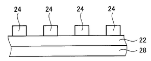
- FIG. 5 is a cross-sectional view taken along the cutting line AA in FIG.
- the capacitive touch panel sensor 180 includes a substrate 22, a first detection electrode 24 disposed on one main surface (surface) of the substrate 22, a first lead-out wiring 26, and the other main surface of the substrate 22.
- a second detection electrode 28, a second lead-out wiring 30, and a flexible printed wiring board 32 are provided on the upper side (on the back surface).
- the region where the first detection electrode 24 and the second detection electrode 28 are provided constitutes an input region E I (an input region (sensing unit) capable of detecting the contact of an object) that can be input by the user, and input.
- a first lead wiring 26, a second lead wiring 30 and a flexible printed wiring board 32 are arranged in the outer region E O located outside the region E I. Below, the said structure is explained in full detail.
- the substrate 22 plays a role of supporting the first detection electrode 24 and the second detection electrode 28 in the input region E I and plays a role of supporting the first lead wiring 26 and the second lead wiring 30 in the outer region E O. It is a member.
- the substrate 22 preferably transmits light appropriately. Specifically, the total light transmittance of the substrate 22 is preferably 85 to 100%.
- the substrate 22 preferably has an insulating property (is an insulating substrate). That is, the substrate 22 is a layer for ensuring insulation between the first detection electrode 24 and the second detection electrode 28.
- the substrate 22 is preferably a transparent substrate (particularly a transparent insulating substrate).
- a transparent substrate particularly a transparent insulating substrate.
- Specific examples thereof include an insulating resin substrate, a ceramic substrate, and a glass substrate.
- an insulating resin substrate is preferable because of its excellent toughness.
- the material constituting the insulating resin substrate is polyethylene terephthalate, polyethersulfone, polyacrylic resin, polyurethane resin, polyester, polycarbonate, polysulfone, polyamide, polyarylate, polyolefin, cellulose resin, poly Examples include vinyl chloride and cycloolefin resins.
- polyethylene terephthalate, cycloolefin resin, polycarbonate, and triacetyl cellulose resin are preferable because of excellent transparency.
- the substrate 22 is a single layer, but may be a multilayer of two or more layers.
- the thickness of the substrate 22 (when the substrate 22 is a multilayer of two or more layers, the total thickness thereof) is not particularly limited, but is preferably 5 to 350 ⁇ m, more preferably 30 to 150 ⁇ m. Within the above range, desired visible light transmittance can be obtained, and handling is easy.
- substrate 22 is substantially rectangular shape, However, It is not restricted to this. For example, it may be circular or polygonal.
- the first detection electrode 24 and the second detection electrode 28 are sensing electrodes that sense a change in capacitance, and constitute a sensing unit (sensor unit). That is, when the fingertip is brought into contact with the touch panel, the mutual capacitance between the first detection electrode 24 and the second detection electrode 28 changes, and the position of the fingertip is calculated by the IC circuit based on the change amount.
- the first detection electrodes 24 are electrodes that extend in a first direction (X direction) and are arranged at a predetermined interval in a second direction (Y direction) orthogonal to the first direction.
- the second detection electrode 28 has a role of detecting the input position in the Y direction of the user's finger approaching the input area E I and has a function of generating a capacitance between the second detection electrode 28 and the finger. ing.
- the second detection electrodes 28 are electrodes that extend in the second direction (Y direction) and are arranged at a predetermined interval in the first direction (X direction), and include a predetermined pattern as will be described later. In FIG. 4, five first detection electrodes 24 and five second detection electrodes 28 are provided, but the number is not particularly limited and may be plural.
- the first detection electrode 24 and the second detection electrode 28 are composed of conductive thin wires.
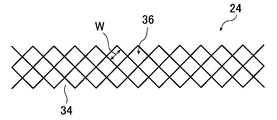
- FIG. 6 shows an enlarged plan view of a part of the first detection electrode 24.
- the first detection electrode 24 is composed of conductive thin wires 34, and includes a plurality of gratings 36 formed of intersecting conductive thin wires 34.
- the second detection electrode 28 similarly to the first detection electrode 24, also includes a plurality of lattices 36 formed by intersecting conductive thin wires 34.
- Examples of the material of the conductive thin wire 34 include metals and alloys such as gold (Au), silver (Ag), copper (Cu), and aluminum (Al), ITO, tin oxide, zinc oxide, cadmium oxide, gallium oxide, Examples thereof include metal oxides such as titanium oxide. Among these, silver is preferable because the conductivity of the conductive thin wire 34 is excellent.
- the conductive fine wire 34 preferably contains a binder from the viewpoint of adhesion between the conductive fine wire 34 and the substrate 22.
- the binder is preferably a water-soluble polymer because the adhesion between the conductive thin wire 34 and the substrate 22 is more excellent.
- the binder include gelatin, carrageenan, polyvinyl alcohol (PVA), polyvinyl pyrrolidone (PVP), polysaccharides such as starch, cellulose and derivatives thereof, polyethylene oxide, polysaccharides, polyvinylamine, chitosan, polylysine, polyacryl. Examples include acid, polyalginic acid, polyhyaluronic acid, carboxycellulose, gum arabic, and sodium alginate.
- gelatin is preferable because the adhesion between the conductive thin wire 34 and the substrate 22 is more excellent.
- acid-processed gelatin may be used as gelatin, and gelatin hydrolyzate, gelatin enzyme decomposition product, and other gelatins modified with amino groups and carboxyl groups (phthalated gelatin, acetylated gelatin) Can be used.
- a polymer different from the above gelatin may be used together with gelatin.
- the type of polymer used is not particularly limited as long as it is different from gelatin.
- the volume ratio of metal to binder (metal volume / binder volume) in the conductive thin wire 34 is preferably 1.0 or more, and more preferably 1.5 or more. By setting the volume ratio of the metal and the binder to 1.0 or more, the conductivity of the conductive thin wire 34 can be further increased.
- the upper limit is not particularly limited, but is preferably 6.0 or less, more preferably 4.0 or less, and even more preferably 2.5 or less from the viewpoint of productivity.
- the volume ratio of the metal and the binder can be calculated from the density of the metal and the binder contained in the conductive thin wire 34. For example, when the metal is silver, the density of silver is 10.5 g / cm 3 , and when the binder is gelatin, the density of gelatin is 1.34 g / cm 3 .
- the line width of the conductive thin wire 34 is not particularly limited, it is preferably 30 ⁇ m or less, more preferably 15 ⁇ m or less, further preferably 10 ⁇ m or less, and particularly preferably 9 ⁇ m or less, from the viewpoint that a low-resistance electrode can be formed relatively easily. 7 ⁇ m or less is most preferable, 0.5 ⁇ m or more is preferable, and 1.0 ⁇ m or more is more preferable.
- the thickness of the conductive thin wire 34 is not particularly limited, but can be selected from 0.00001 mm to 0.2 mm from the viewpoint of conductivity and visibility, but is preferably 30 ⁇ m or less, more preferably 20 ⁇ m or less, and 0.01 Is more preferably from 9 to 9 ⁇ m, most preferably from 0.05 to 5 ⁇ m.
- the lattice 36 includes an opening region surrounded by the thin conductive wires 34.
- the length W of one side of the grating 36 is preferably 800 ⁇ m or less, more preferably 600 ⁇ m or less, and preferably 400 ⁇ m or more.
- the aperture ratio is preferably 85% or more, more preferably 90% or more, and most preferably 95% or more in terms of visible light transmittance. preferable.
- the aperture ratio corresponds to the ratio of the transmissive portion excluding the conductive thin wires 34 in the first detection electrode 24 or the second detection electrode 28 in the predetermined region.
- the lattice 36 has a substantially rhombus shape.
- other polygonal shapes for example, a triangle, a quadrangle, and a hexagon
- the shape of one side may be a curved shape or a circular arc shape in addition to a linear shape.
- the arc shape for example, the two opposing sides may have an outwardly convex arc shape, and the other two opposing sides may have an inwardly convex arc shape.
- the shape of each side may be a wavy shape in which an outwardly convex arc and an inwardly convex arc are continuous.
- the shape of each side may be a sine curve.
- the conductive thin wire 34 is formed as a mesh pattern, but is not limited to this mode, and may be a stripe pattern.
- the first lead wiring 26 and the second lead wiring 30 are members that play a role in applying a voltage to the first detection electrode 24 and the second detection electrode 28, respectively.
- the first lead wiring 26 is disposed on the substrate 22 in the outer region E O , one end of which is electrically connected to the corresponding first detection electrode 24, and the other end is electrically connected to the flexible printed wiring board 32.
- the second lead wiring 30 is disposed on the substrate 22 in the outer region E O , one end of which is electrically connected to the corresponding second detection electrode 28, and the other end is electrically connected to the flexible printed wiring board 32.
- the In FIG. 4, five first extraction wirings 26 and five second extraction wirings 30 are illustrated, but the number is not particularly limited, and a plurality of the first extraction wirings are usually arranged according to the number of detection electrodes.
- Examples of the material constituting the first lead wiring 26 and the second lead wiring 30 include metals such as gold (Au), silver (Ag), and copper (Cu), tin oxide, zinc oxide, cadmium oxide, and gallium oxide. And metal oxides such as titanium oxide.
- silver is preferable because of its excellent conductivity.
- a metal paste a screen printing or ink jet printing method is used, and in the case of a metal or alloy thin film, a patterning method such as a photolithography method is suitably used for the sputtered film.
- the binder is contained in the 1st extraction wiring 26 and the 2nd extraction wiring 30 from the point which adhesiveness with the board
- the kind of binder is as above-mentioned.
- the flexible printed wiring board 32 is a board in which a plurality of wirings and terminals are provided on a substrate, and is connected to each other end of the first lead wiring 26 and each other end of the second lead wiring 30 to electrostatically It plays a role of connecting the capacitive touch panel sensor 180 and an external device (for example, a display device).
- the manufacturing method of the capacitive touch panel sensor 180 is not particularly limited, and a known method can be adopted. For example, there is a method in which a photoresist film on the metal foil formed on both main surfaces of the substrate 22 is exposed and developed to form a resist pattern, and the metal foil exposed from the resist pattern is etched. Further, there is a method in which a paste containing metal fine particles or metal nanowires is printed on both main surfaces of the substrate 22 and metal plating is performed on the paste. Moreover, the method of printing and forming on the board
- a method using silver halide can be mentioned. More specifically, the step (1) of forming a silver halide emulsion layer (hereinafter also referred to simply as a photosensitive layer) containing silver halide and a binder on both surfaces of the substrate 22, respectively, exposing the photosensitive layer. Then, the method which has the process (2) which carries out image development processing is mentioned. Below, each process is demonstrated.
- a silver halide emulsion layer hereinafter also referred to simply as a photosensitive layer
- Step (1) is a step of forming a photosensitive layer containing silver halide and a binder on both surfaces of the substrate 22.
- the method for forming the photosensitive layer is not particularly limited, but from the viewpoint of productivity, the photosensitive layer forming composition containing silver halide and a binder is brought into contact with the substrate 22, and the photosensitive layer is formed on both surfaces of the substrate 22.
- the method of forming is preferred. Below, after explaining in full detail the aspect of the composition for photosensitive layer formation used with the said method, the procedure of a process is explained in full detail.
- the photosensitive layer forming composition contains a silver halide and a binder.
- the halogen element contained in the silver halide may be any of chlorine, bromine, iodine and fluorine, or a combination thereof.
- As the silver halide for example, silver halides mainly composed of silver chloride, silver bromide and silver iodide are preferably used, and silver halides mainly composed of silver bromide and silver chloride are preferably used.
- the kind of binder used is as above-mentioned.
- the binder may be contained in the composition for photosensitive layer formation in the form of latex.
- the volume ratio of the silver halide and the binder contained in the composition for forming the photosensitive layer is not particularly limited, and is appropriately adjusted so as to be within a preferable volume ratio range of the metal and the binder in the conductive thin wire 34 described above. Is done.
- the composition for forming a photosensitive layer contains a solvent, if necessary.
- the solvent used include water, organic solvents (for example, alcohols such as methanol, ketones such as acetone, amides such as formamide, sulfoxides such as dimethyl sulfoxide, esters such as ethyl acetate, ethers, and the like. Etc.), ionic liquids, or mixed solvents thereof.
- the content of the solvent to be used is not particularly limited, but is preferably in the range of 30 to 90% by mass, and more preferably in the range of 50 to 80% by mass with respect to the total mass of silver halide and binder.
- the method for bringing the composition for forming a photosensitive layer and the substrate 22 into contact with each other is not particularly limited, and a known method can be adopted.
- substrate 22 in the composition for photosensitive layer formation, etc. are mentioned.
- the content of the binder in the formed photosensitive layer is not particularly limited but is preferably 0.3 ⁇ 5.0g / m 2, more preferably 0.5 ⁇ 2.0g / m 2.
- the content of the silver halide in the photosensitive layer is not particularly limited, but is preferably 1.0 to 20.0 g / m 2 in terms of silver from the viewpoint that the conductive properties of the conductive fine wire 34 are more excellent. 0 to 15.0 g / m 2 is more preferable.
- the protective layer By providing the protective layer, scratches can be prevented and mechanical properties can be improved.
- Step (2) Exposure development process>
- the photosensitive layer obtained in the above step (1) is subjected to pattern exposure and then developed to thereby perform the first detection electrode 24 and the first lead wiring 26, and the second detection electrode 28 and the second detection electrode 28.
- This is a step of forming two lead-out wirings 30.
- the pattern exposure process will be described in detail below, and then the development process will be described in detail.
- the silver halide in the photosensitive layer in the exposed region forms a latent image.
- conductive thin lines are formed by a development process described later.
- the silver halide dissolves and flows out of the photosensitive layer during the fixing process described later, and a transparent film is obtained.
- the light source used in the exposure is not particularly limited, and examples thereof include light such as visible light and ultraviolet light, and radiation such as X-rays.
- the method for performing pattern exposure is not particularly limited. For example, surface exposure using a photomask may be performed, or scanning exposure using a laser beam may be performed.
- the shape of the pattern is not particularly limited, and is appropriately adjusted according to the pattern of the conductive fine wire to be formed.
- the development processing method is not particularly limited, and a known method can be employed.
- a usual development processing technique used for silver salt photographic film, photographic paper, film for printing plate making, emulsion mask for photomask, and the like can be used.
- the type of the developer used in the development process is not particularly limited.
- PQ developer, MQ developer, MAA developer and the like can be used.
- Commercially available products include, for example, CN-16, CR-56, CP45X, FD-3, Papitol, C-41, E-6, RA-4, D-19, D-72 prescribed by KODAK.
- a developer contained in a kit thereof can be used.
- a lith developer can also be used.
- the development process can include a fixing process performed for the purpose of removing and stabilizing the silver salt in the unexposed part.
- a technique of fixing process used for silver salt photographic film, photographic paper, film for printing plate making, emulsion mask for photomask and the like can be used.
- the fixing temperature in the fixing step is preferably about 20 ° C. to about 50 ° C., more preferably 25 to 45 ° C.
- the fixing time is preferably 5 seconds to 1 minute, more preferably 7 seconds to 50 seconds.
- the mass of the metallic silver contained in the exposed area (conductive thin wire) after the development treatment is preferably a content of 50% by mass or more based on the mass of silver contained in the exposed area before the exposure, More preferably, it is at least mass%. If the mass of silver contained in the exposed portion is 50% by mass or more based on the mass of silver contained in the exposed portion before exposure, it is preferable because high conductivity can be obtained.
- the following undercoat layer forming step, antihalation layer forming step, or heat treatment may be performed as necessary.
- Undercoat layer forming process For the reason of excellent adhesion between the substrate 22 and the silver halide emulsion layer, it is preferable to perform a step of forming an undercoat layer containing the binder on both sides of the substrate 22 before the step (1).
- the binder used is as described above.
- the thickness of the undercoat layer is not particularly limited, but is preferably from 0.01 to 0.5 ⁇ m, more preferably from 0.01 to 0.1 ⁇ m, from the viewpoint that the adhesiveness and the rate of change in mutual capacitance can be further suppressed.
- Anti-halation layer formation process From the viewpoint of thinning the conductive thin wire 34, it is preferable to carry out a step of forming antihalation layers on both surfaces of the substrate 22 before the step (1).
- Step (3) is a step of performing heat treatment after the development processing. By performing this step, fusion occurs between the binders, and the hardness of the conductive thin wires 34 is further increased.
- the binder when polymer particles are dispersed as a binder in the composition for forming a photosensitive layer (when the binder is polymer particles in latex), by performing this step, fusion occurs between the polymer particles, Conductive thin wires 34 having a desired hardness are formed.
- the conditions for the heat treatment are appropriately selected depending on the binder to be used, but it is preferably 40 ° C. or higher from the viewpoint of the film forming temperature of the polymer particles, more preferably 50 ° C. or higher, and further 60 ° C. or higher.
- the heating time is not particularly limited, but is preferably 1 to 5 minutes and more preferably 1 to 3 minutes from the viewpoint of suppressing curling of the substrate and the like and productivity.
- this heat treatment can be combined with a drying step usually performed after exposure and development processing, it is not necessary to increase a new step for film formation of polymer particles, and productivity, cost, etc. Excellent from a viewpoint.
- the light transmissive part containing a binder is formed between the electroconductive thin wires 34.
- FIG. The transmittance in the light-transmitting portion is preferably 90% or more, more preferably 95% or more, still more preferably 97% or more, and more preferably 98% or more, as shown by the minimum transmittance in the wavelength region of 380 to 780 nm. Is particularly preferable, and 99% or more is most preferable.
- the light transmissive portion may contain materials other than the binder, and examples thereof include a silver difficult solvent.
- the capacitive touch panel sensor is not limited to the aspect of FIG. 4 described above, and may be another aspect.
- the capacitive touch panel sensor 280 is electrically connected to the first substrate 38, the second detection electrode 28 disposed on the first substrate 38, and one end of the second detection electrode 28. And electrically connected to one end of the second lead-out wiring (not shown) disposed on the first substrate 38, the adhesive sheet 40, the first detection electrode 24, and the first detection electrode 24.
- the capacitive touch panel sensor 280 has the same configuration as the capacitive touch panel sensor 180 except for the first substrate 38, the second substrate 42, and the adhesive sheet 40. Therefore, the same components are denoted by the same reference numerals, and the description thereof is omitted.
- the definitions of the first substrate 38 and the second substrate 42 are the same as the definition of the substrate 22 described above.
- the pressure-sensitive adhesive sheet 40 is a layer for bringing the first detection electrode 24 and the second detection electrode 28 into close contact with each other, and is preferably optically transparent (preferably a transparent pressure-sensitive adhesive sheet).
- a known material may be used as the material constituting the pressure-sensitive adhesive sheet 40, and the pressure-sensitive adhesive sheet 12 may be used as the pressure-sensitive adhesive sheet 40.
- a plurality of the first detection electrodes 24 and the second detection electrodes 28 in FIG. 7 are used as shown in FIG. 4, and both are arranged so as to be orthogonal to each other as shown in FIG.
- the capacitive touch panel sensor 280 shown in FIG. 7 is prepared by preparing two substrates with electrodes having a substrate and detection electrodes and lead wires arranged on the substrate surface, so that the electrodes face each other. Corresponds to the capacitive touch panel sensor obtained by bonding through the.
- the capacitive touch panel sensor 380 is electrically connected to the first substrate 38, the second detection electrode 28 disposed on the first substrate 38, and one end of the second detection electrode 28.
- a second lead-out wiring (not shown), an adhesive sheet 40, a second substrate 42, a first detection electrode 24 disposed on the second substrate 42, and one end of the first detection electrode 24;
- a first lead-out wiring (not shown) and a flexible printed wiring board (not shown) which are electrically connected and are arranged on the second substrate 42 are provided.
- the capacitive touch panel sensor 380 shown in FIG. 8 has the same layers as the capacitive touch panel sensor 280 shown in FIG. 7 except that the order of the layers is different.
- the capacitive touch panel sensor 380 shown in FIG. 8 prepares two substrates with electrodes having a substrate and detection electrodes and lead wires arranged on the substrate surface, and the substrate in the substrate with one electrode It corresponds to the electrostatic capacitance type touch panel sensor obtained by bonding through an adhesive sheet so that the electrode of the other board
- the conductive thin wires 34 of the first detection electrode 24 and the second detection electrode 28 are made of metal oxide particles, metal such as silver paste or copper paste. You may be comprised with the paste. Among these, a conductive film made of a thin silver wire and a silver nanowire conductive film are preferable in terms of excellent conductivity and transparency.
- the first detection electrode 24 and the second detection electrode 28 are configured by the mesh structure of the conductive thin wires 34.
- the present invention is not limited to this mode.
- a metal oxide thin film (transparent metal) such as ITO or ZnO is used.
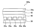
- FIG. 9 is a partial plan view of the input area of the capacitive touch panel sensor 180a.
- FIG. 10 is a cross-sectional view taken along the cutting line AA in FIG.
- the capacitive touch panel sensor 180a is electrically connected to the first substrate 38, the second detection electrode 28a disposed on the first substrate 38, and one end of the second detection electrode 28a.
- a second lead-out wiring (not shown), an adhesive sheet 40, a second substrate 42, a first detection electrode 24a disposed on the second substrate 42, and one end of the first detection electrode 24a.
- a first lead-out wiring (not shown) and a flexible printed wiring board (not shown) which are electrically connected and are arranged on the second substrate 42 are provided.
- the capacitive touch panel sensor 180a shown in FIGS. 9 and 10 has the same layer as the capacitive touch panel sensor 380 shown in FIG. 8 except for the points other than the first detection electrode 24a and the second detection electrode 28a. Therefore, the same components are denoted by the same reference numerals, and the description thereof is omitted.
- the first detection electrode 24a and the second detection electrode 28a are electrodes extending in the X-axis direction and the Y-axis direction, respectively, and are made of a transparent metal oxide, for example, indium tin oxide (ITO).
- ITO indium tin oxide
- the 9 and 10 in order to make use of the transparent electrode ITO as a sensor, the resistance of the indium tin oxide (ITO) itself is increased, the total wiring resistance is reduced by increasing the electrode area, and the thickness is further increased. It is designed to ensure the light transmittance by making it thinner and taking advantage of the characteristics of the transparent electrode.
- examples of materials that can be used in the above embodiment include zinc oxide (ZnO), indium zinc oxide (IZO), gallium zinc oxide (GZO), and aluminum zinc oxide (AZO). It is done.
- the patterning of the electrode parts can be selected according to the material of the electrode part, and includes a photolithography method, a resist mask screen printing-etching method, an inkjet method, a printing method, and the like. It may be used.
- the protective substrate 20 is a substrate disposed on the adhesive sheet, and serves to protect a capacitive touch panel sensor 18 (to be described later) from the external environment, and its main surface constitutes a touch surface.
- the protective substrate 20 is preferably a transparent substrate, and a plastic film, a plastic plate, a glass plate, or the like is used. It is desirable that the thickness of the substrate is appropriately selected according to each application.
- polyesters such as polyethylene terephthalate (PET) and polyethylene naphthalate (PEN); polyolefins such as polyethylene (PE), polypropylene (PP), polystyrene, and EVA; Resin;
- polycarbonate (PC) polyamide, polyimide, acrylic resin, triacetyl cellulose (TAC), cycloolefin resin (COP), and the like can be used.
- a polarizing plate, a circular polarizing plate, or the like may be used as the protective substrate 20 .
- the protective substrate integrated capacitive touch panel sensor 60 is a member in which a protective substrate and a capacitive touch panel sensor are integrated.
- the method for manufacturing the protective substrate integrated capacitive touch panel sensor 60 is not particularly limited, and examples thereof include a method of directly forming a detection electrode on the protective substrate.
- the display device 50 is a device having a display surface for displaying an image, and each member is arranged on the display screen side.
- the type of the display device 50 is not particularly limited, and a known display device can be used.
- cathode ray tube (CRT) display liquid crystal display (LCD), organic light emitting diode (OLED) display, vacuum fluorescent display (VFD), plasma display panel (PDP), surface field display (SED) or field emission display (FED) or electronic paper (E-Paper).
- CTR cathode ray tube
- LCD liquid crystal display
- OLED organic light emitting diode
- VFD vacuum fluorescent display
- PDP plasma display panel
- SED surface field display
- FED field emission display
- E-Paper electronic paper
- the above-mentioned pressure-sensitive adhesive sheet of the present invention can be suitably used for the production of a capacitive touch panel.
- a capacitive touch panel For example, between the display device and the capacitive touch panel sensor, between the capacitive touch panel sensor and a protective substrate, or on the substrate and the substrate in the capacitive touch sensor. It is used to provide an adhesive sheet that is disposed between conductive films provided with detection electrodes.
- the pressure-sensitive adhesive sheet of the present invention is preferably used for providing a pressure-sensitive adhesive layer adjacent to the detection electrode in the capacitive touch panel. When used in such an aspect, it is preferable because touch malfunctions due to the influence of the above-described variation factors can be remarkably reduced.
- the adhesive sheet is adjacent to the detection electrode
- the capacitive touch panel sensor has a configuration in which the detection electrode is arranged on the back surface of the substrate, the detection electrode is in contact with both detection electrodes.
- an adhesive sheet is arrange
- the capacitive touch panel sensor has two conductive films each having a substrate and a detection electrode disposed on one side of the substrate, and the two conductive films are detected when bonded.
- positioned so that an electrode may be touched is mentioned. More specifically, the case where it uses as an aspect of the adhesive sheet 40 of FIG. 7 and FIG. 8 is mentioned.
- the pressure-sensitive adhesive composition of Example 1 includes EHMA (20 parts by mass), FA-512M (5 parts by mass), TPO (2.4 parts by mass), IRG819 (0.6 parts by mass), A pressure-sensitive adhesive composition obtained by mixing and stirring UC-203 (21.78 parts by mass), P-135 (38.8 parts by mass), and Polyoil 110 (11.42 parts by mass). is there. Details of each component are as described below. In the examples and comparative examples other than comparative examples 8 and 14, a homogeneous composition was obtained. On the other hand, in Comparative Examples 8 and 14, IRG819 (Irgacure 819) was not compatible with other components, and a homogeneous composition capable of forming an adhesive sheet was not obtained.
- the largest value of less than 20 ⁇ m is designated as “A” as having excellent step followability, and those having 20 ⁇ m or more but less than 50 ⁇ m are designated as “B” having relatively excellent step followability, A material having a thickness of 50 ⁇ m or more and less than 100 ⁇ m is not preferable, but “C” is used as a practically usable product, and a product having a size of 100 ⁇ m or more is “D” because it is inferior in level-step following and has no practicality.
- Table 1 The results are shown in Table 1.
- the emulsion after washing with water and desalting was adjusted to pH 6.4 and pAg 7.5, and gelatin 3.9 g, sodium benzenethiosulfonate 10 mg, sodium benzenethiosulfinate 3 mg, sodium thiosulfate 15 mg and chloroauric acid 10 mg were added.
- Chemical sensitization to obtain optimum sensitivity at 0 ° C. 100 mg of 1,3,3a, 7-tetraazaindene as stabilizer and 100 mg of proxel (trade name, manufactured by ICI Co., Ltd.) as preservative It was.
- the finally obtained emulsion contains 0.08 mol% of silver iodide, and the ratio of silver chlorobromide is 70 mol% of silver chloride and 30 mol% of silver bromide. It was a silver iodochlorobromide cubic grain emulsion having a coefficient of 9%.
- Photosensitive layer forming step After subjecting a polyethylene terephthalate (PET) film having a thickness of 100 ⁇ m to corona discharge treatment, a gelatin layer having a thickness of 0.1 ⁇ m as an undercoat layer on both sides of the PET film, and an optical density of about 1.0 on the undercoat layer. And an antihalation layer containing a dye which is decolorized by alkali in the developer. On the antihalation layer, the composition for forming a photosensitive layer was applied, a gelatin layer having a thickness of 0.15 ⁇ m was further provided, and a PET film having a photosensitive layer formed on both sides was obtained. The obtained film is referred to as film A.
- the formed photosensitive layer had a silver amount of 6.0 g / m 2 and a gelatin amount of 1.0 g / m 2 .
- Exposure development process As shown in FIG. 4, a high voltage is applied through a photomask in which detection electrodes (first detection electrodes and second detection electrodes) and lead wires (first lead wires and second lead wires) are arranged on both surfaces of the film A. Exposure was performed using parallel light using a mercury lamp as a light source. After the exposure, development was performed with the following developer, and further development was performed using a fixer (trade name: N3X-R for CN16X, manufactured by Fuji Film). Furthermore, by rinsing with pure water and drying, a capacitive touch panel sensor A provided with detection electrodes and lead wires made of Ag fine wires on both sides was obtained.
- the detection electrodes are composed of conductive thin wires that intersect in a mesh shape. Further, as described above, the first detection electrode is an electrode extending in the X direction, and the second detection electrode is an electrode extending in the Y direction, and each is disposed on the film at a pitch of 4.5 to 5 mm.
- a touch panel including a liquid crystal display device, a lower adhesive layer, a capacitive touch panel sensor, an upper adhesive layer, and a glass substrate in this order was manufactured.
- the capacitive touch panel sensor A manufactured above was used as a capacitive touch panel sensor.
- the upper adhesive layer was formed by pasting using a 2 kg heavy roller so that the surface of the upper surface would face.
- the release PET of the pressure-sensitive adhesive sheet was peeled off, and a glass substrate of the same size was bonded onto the upper pressure-sensitive adhesive layer in the same manner using a 2 kg heavy roller. Then, it was exposed to the environment of 40 degreeC and 5 atmospheres for 20 minutes in the high-pressure thermostat, and the defoaming process was performed. Next, following the same procedure as the formation of the upper adhesive layer, an adhesive sheet (having a release PET on one side) is bonded to the surface opposite to the surface on which the upper adhesive layer of the capacitive touch panel A is formed, A lower adhesive layer was formed. Furthermore, the release PET of the pressure-sensitive adhesive sheet was peeled off, and a liquid crystal display device was attached on the lower pressure-sensitive adhesive layer. Then, it was exposed to the environment of 40 degreeC and 5 atmospheres for 20 minutes in the high-pressure thermostat, and the defoaming process was performed. Thus, the touch panel was manufactured.
- the obtained touch panel was heated stepwise from ⁇ 40 ° C. to 80 ° C. in steps of 20 ° C., and the malfunction occurrence rate at the time of touch at each temperature was obtained. That is, in an environment of ⁇ 40 ° C., ⁇ 20 ° C., 0 ° C., 20 ° C., 40 ° C., 60 ° C., and 80 ° C., an arbitrary location is touched 100 times and the touch panel The occurrence rate of malfunction (%) [(number of times of not reacting normally / 100) ⁇ 100] was determined.
- the highest value of less than 5% is regarded as “A” as the malfunction occurrence rate is very low, and the malfunction occurrence rate is relatively high when the malfunction occurrence rate is 5% or more and less than 10%.
- Table 1 The results are shown in Table 1.
- b / a means “the solubility parameter (SP value) is 8.0 to 10.0, and a branched alkyl group and an alicyclic hydrocarbon group (however, an unsaturated hydrocarbon group) Content (b) of a radically polymerizable monomer (B) having at least one group selected from the group consisting of: an alicyclic hydrocarbon group having a monovalent phosphine oxide (A1) and bis The mass ratio (b / a) to the total content (a) of the acylphosphine oxide (A2) is represented.
- EHMA, CHMA, IBXA and IBX correspond to the radical polymerizable monomer (B)
- HEMA, MMA, FA-512M, FA-512AS, EHA and StMA are the radical polymerization monomers. It does not fall under the sex monomer (B).
- O / C ratio represents the ratio between the number of moles of oxygen atoms and the number of moles of carbon atoms contained in the pressure-sensitive adhesive composition (number of moles of oxygen atoms / number of moles of carbon atoms).
- EHMA 2-ethylhexyl methacrylate (SP value: 8.1)
- CHMA cyclohexyl methacrylate (SP value: 8.3)
- IBXA isobornyl acrylate (SP value: 8.33)
- -HEMA 2-hydroxyethyl methacrylate (SP value: 9.39)
- MMA Methyl methacrylate (SP value: 8.2)
- FA-512M dicyclopentenyloxyethyl methacrylate, manufactured by Hitachi Chemical Co., Ltd.
- FA-512AS dicyclopentenyloxyethyl acrylate, manufactured by Hitachi Chemical Co., Ltd.
- EHA 2-ethylhexyl acrylate (SP value: 7.8)
- IBX isobornyl methacrylate (SP value: 8.3)
- StMA Stearyl methacrylate
- TPO Lucirin TPO (2,4,6-trimethylbenzoyl-diphenylphosphine oxide, manufactured by BASF) (absorbance at 400 nm of 0.1% by weight acetonitrile solution: 1.0)
- TPO-L Lucirin TPO-L (2,4,6-trimethylbenzoyl-phenylethoxyphosphine oxide, manufactured by BASF) (absorbance at 400 nm of 0.1 mass% acetonitrile solution: 0.4)
- IRG819 Irgacure 819 (bis (2,4,6-trimethylbenzoyl) -phenylphosphine oxide, manufactured by BASF) (absorbance at 430 nm of 0.1 mass% acetonitrile solution: 0.25)
- Examples 2 and 3 which are the above, exhibited better adhesion and step following ability. Especially, Example 3 whose mass ratio (a2 / a1) was 0.40 or more showed the further outstanding adhesiveness. From the comparison of Examples 3 to 5, the mass of the content (b) of the radical polymerizable monomer (B) and the total content (a) of the monoacylphosphine oxide (A1) and the bisacylphosphine oxide (A2). Examples 3 and 4 having a ratio (b / a) of 4.0 or more exhibited better adhesion and step following ability. Further, from the comparison of Examples 3 to 4 and 17 to 18, Examples 3 and 17 in which the mass ratio (b / a) is 6.0 or more show further excellent step followability and more malfunctions occur. It was suppressed.
- Comparative Examples 1 to 5 and 7 using only the monoacylphosphine oxide (A1) without using the monoacylphosphine oxide (A1) and the bisacylphosphine oxide (A2) together have insufficient adhesion. there were. In addition, the malfunction occurrence rate may be high.
- Comparative Example 8 using only bisacylphosphine oxide (A2) a homogeneous composition capable of forming an adhesive sheet was not obtained.
- Comparative Examples 11 to 13 and 15 in which the monoacylphosphine oxide (A1) and the bisacylphosphine oxide (A2) are used in combination but the specific radical polymerizable monomer (B) is not used have insufficient adhesion, Moreover, the malfunction occurrence rate was high.
- monoacylphosphine oxide (A1) and bisacylphosphine oxide (A2) are used in combination, and a specific radical polymerizable monomer (B) is used, but the mass ratio (b / a) is less than 3.0.
- a homogeneous composition capable of forming an adhesive sheet could not be obtained.
- the monoacylphosphine oxide (A1) and the bisacylphosphine oxide (A2) are used in combination, and the specific radical polymerizable monomer (B) is used.
- Comparative Example 6 in which the amount was less than 1.5% by mass, the adhesion was insufficient and the malfunction occurrence rate was high.
- Adhesive sheets 18, 180, 180 a, 280, 380 Capacitive touch panel sensor 20
- Substrate 24 24
- a First extraction wiring 28, 28 a Second detection electrode 30
- Second extraction wiring 32
- Flexible printed wiring board 34 Conductive thin wire 36
- Grid 38 First substrate
- Adhesive sheet 42 Second substrate 50
- Display device 60 Integrated protective substrate capacitive touch panel sensor 100, 200 Laminate 300, 400, 500 for touch panel Capacitance Touch panel
Landscapes
- Engineering & Computer Science (AREA)
- Chemical & Material Sciences (AREA)
- Theoretical Computer Science (AREA)
- General Engineering & Computer Science (AREA)
- Organic Chemistry (AREA)
- Medicinal Chemistry (AREA)
- Polymers & Plastics (AREA)
- Health & Medical Sciences (AREA)
- Chemical Kinetics & Catalysis (AREA)
- Human Computer Interaction (AREA)
- Physics & Mathematics (AREA)
- General Physics & Mathematics (AREA)
- Adhesive Tapes (AREA)
- Adhesives Or Adhesive Processes (AREA)
- Polarising Elements (AREA)
Abstract
本発明は、粘着シートとしたときに密着性に優れ、かつ、粘着シートとして静電容量式タッチパネルに用いたときに、低温から高温までの幅広い温度環境下にて誤動作の発生を抑制することができる粘着剤組成物、該組成物から得られる粘着シート、該粘着シートを備えるタッチパネル用積層体および静電容量式タッチパネルセンサーを提供することを目的とする。本発明の粘着剤組成物は、モノアシルホスフィンオキサイドA1と、ビスアシルホスフィンオキサイドA2と、特定の基を有する所定の溶解度パラメータのラジカル重合性モノマーBとを含有する粘着剤組成物であって、上記組成物の全量に対する上記A1の含有量が、1.5質量%以上であり、上記Bの含有量bと、上記A1および上記A2の合計の含有量aとの質量比b/aが、3.0~30.0であり、上記組成物に含まれる酸素原子のモル数と炭素原子のモル数との比が、0.1以下である。
Description
本発明は、粘着剤組成物、粘着シート(特にタッチパネル用粘着シート)、タッチパネル用積層体および静電容量式タッチパネルに関する。
近年、携帯電話や携帯ゲーム機器等へのタッチパネルの搭載率が上昇しており、例えば、多点検出が可能な静電容量方式のタッチパネル(以後、単にタッチパネルとも称する)が注目を集めている。
通常、タッチパネルを製造する際には、表示装置やタッチパネルセンサーなどの各部材間を密着させるために粘着剤組成物や接着剤組成物が使用されている。なお、これらの組成物はシート状に成形されて使用されることが多い。
通常、タッチパネルを製造する際には、表示装置やタッチパネルセンサーなどの各部材間を密着させるために粘着剤組成物や接着剤組成物が使用されている。なお、これらの組成物はシート状に成形されて使用されることが多い。
例えば、特許文献1には、(メタ)アクリレート系モノマーとLucirin TPO(モノアシルホスフィンオキサイド)とを含有するタッチパネル用の接着剤組成物が開示されている(実施例)。
一方で、粘着剤組成物から得られる粘着シートは、タッチパネルに用いる上で様々な特性が求められる。例えば、タッチパネルの耐久性の点から優れた密着性が求められる。また、タッチパネルの環境適応性の点から、冷地や温暖地など様々な使用環境下において、誤動作が生じ難いことが求められる。すなわち、誤動作発生率が低いことが求められる。
このようななか本発明者らが、特許文献1を参考に、ラジカル重合性モノマーとモノアシルホスフィンオキサイドとを含有する粘着剤組成物を用いて粘着シートを形成したところ、その密着性は昨今求められるレベルを満たすものではないことが明らかになった。また、上記粘着シートをタッチパネルに用いたところ、誤動作発生率は昨今求められるレベルを必ずしも満たすものではないことが明らかになった。
そこで、本発明は、上記実情を鑑みて、粘着シートとしたときに密着性に優れ、かつ、粘着シートとして静電容量式タッチパネルに用いたときに、低温から高温までの幅広い温度環境下にて誤動作の発生を抑制することができる粘着剤組成物を提供することを目的とする。
本発明者らは、上記課題について鋭意検討した結果、モノアシルホスフィンオキサイドに加えてビスアシルホスフィンオキサイドを併用し、かつ、ラジカル重合性モノマーとして特定のモノマーを使用するとともに、粘着剤組成物に含まれる酸素原子のモル数と炭素原子のモル数との比を特定にすることで上記課題が解決できることを見出し、本発明に至った。
すなわち、本発明者らは、以下の構成により上記課題が解決できることを見出した。
すなわち、本発明者らは、以下の構成により上記課題が解決できることを見出した。
(1) モノアシルホスフィンオキサイド(A1)と、ビスアシルホスフィンオキサイド(A2)と、溶解度パラメータ(SP値)が8.0~10.0であるラジカル重合性モノマー(B)とを含有する粘着剤組成物であって、
上記ラジカル重合性モノマー(B)が、分岐状アルキル基および脂環式炭化水素基(ただし、不飽和炭化水素基を有する脂環式炭化水素基を除く)からなる群より選択される少なくとも1種の基を有し、
上記粘着剤組成物の全量に対する上記モノアシルホスフィンオキサイド(A1)の含有量が、1.5質量%以上であり、
上記ラジカル重合性モノマー(B)の含有量(b)と、上記モノアシルホスフィンオキサイド(A1)および上記ビスアシルホスフィンオキサイド(A2)の合計の含有量(a)との質量比(b/a)が、3.0~30.0であり、
上記粘着剤組成物に含まれる酸素原子のモル数と炭素原子のモル数との比(酸素原子のモル数/炭素原子のモル数)が、0.1以下である、粘着剤組成物。
(2) さらに、アミノケトン系光重合開始剤およびヒドロキシケトン系光重合開始剤からなる群より選択される少なくとも1種の光重合開始剤を含有する、上記(1)に記載の粘着剤組成物。
(3) さらに、後述する一般式(I)で表される増感色素を含有する、上記(1)または(2)に記載の粘着剤組成物。
(4) さらに、亜リン酸エステル、アミンおよびチオールからなる群より選択される少なくとも1種の重合阻害抑制剤を含有する、上記(1)~(3)のいずれかに記載の粘着剤組成物。
(5) 上記(1)~(4)のいずれかに記載の粘着剤組成物から得られる粘着シート。
(6) 厚みが50μm以上である、上記(5)に記載の粘着シート。
(7) タッチパネル用粘着シートである、上記(5)または(6)に記載の粘着シート。
(8) 上記(7)に記載の粘着シートと、静電容量式タッチパネルセンサーとを備える、タッチパネル用積層体。
(9) さらに、保護基板を備え、
上記保護基板と、上記粘着シートと、上記静電容量式タッチパネルセンサーとをこの順に備える、上記(8)に記載のタッチパネル用積層体。
(10) 静電容量式タッチパネルセンサーと、上記(7)に記載の粘着シートと、表示装置とをこの順に備える、静電容量式タッチパネル。
上記ラジカル重合性モノマー(B)が、分岐状アルキル基および脂環式炭化水素基(ただし、不飽和炭化水素基を有する脂環式炭化水素基を除く)からなる群より選択される少なくとも1種の基を有し、
上記粘着剤組成物の全量に対する上記モノアシルホスフィンオキサイド(A1)の含有量が、1.5質量%以上であり、
上記ラジカル重合性モノマー(B)の含有量(b)と、上記モノアシルホスフィンオキサイド(A1)および上記ビスアシルホスフィンオキサイド(A2)の合計の含有量(a)との質量比(b/a)が、3.0~30.0であり、
上記粘着剤組成物に含まれる酸素原子のモル数と炭素原子のモル数との比(酸素原子のモル数/炭素原子のモル数)が、0.1以下である、粘着剤組成物。
(2) さらに、アミノケトン系光重合開始剤およびヒドロキシケトン系光重合開始剤からなる群より選択される少なくとも1種の光重合開始剤を含有する、上記(1)に記載の粘着剤組成物。
(3) さらに、後述する一般式(I)で表される増感色素を含有する、上記(1)または(2)に記載の粘着剤組成物。
(4) さらに、亜リン酸エステル、アミンおよびチオールからなる群より選択される少なくとも1種の重合阻害抑制剤を含有する、上記(1)~(3)のいずれかに記載の粘着剤組成物。
(5) 上記(1)~(4)のいずれかに記載の粘着剤組成物から得られる粘着シート。
(6) 厚みが50μm以上である、上記(5)に記載の粘着シート。
(7) タッチパネル用粘着シートである、上記(5)または(6)に記載の粘着シート。
(8) 上記(7)に記載の粘着シートと、静電容量式タッチパネルセンサーとを備える、タッチパネル用積層体。
(9) さらに、保護基板を備え、
上記保護基板と、上記粘着シートと、上記静電容量式タッチパネルセンサーとをこの順に備える、上記(8)に記載のタッチパネル用積層体。
(10) 静電容量式タッチパネルセンサーと、上記(7)に記載の粘着シートと、表示装置とをこの順に備える、静電容量式タッチパネル。
以下に示すように、本発明によれば、粘着シートとしたときに密着性に優れ、かつ、粘着シートとして静電容量式タッチパネルに用いたときに、低温から高温までの幅広い温度環境下にて誤動作の発生を抑制することができる粘着剤組成物を提供することができる。
以下に、本発明の粘着剤組成物、並びに、本発明の粘着剤組成物を用いた粘着シート、タッチパネル用積層体および静電容量式タッチパネルについて説明する。
なお、本明細書において、(メタ)アクリレートとは、アクリレートまたはメタクリレートを表し、(メタ)アクリロイル基とは、アクリロイル基またはメタクリロイル基を表す。
さらに、本明細書において「~」を用いて表される数値範囲は、「~」の前後に記載される数値を下限値および上限値として含む範囲を意味する。
なお、本明細書において、(メタ)アクリレートとは、アクリレートまたはメタクリレートを表し、(メタ)アクリロイル基とは、アクリロイル基またはメタクリロイル基を表す。
さらに、本明細書において「~」を用いて表される数値範囲は、「~」の前後に記載される数値を下限値および上限値として含む範囲を意味する。
[粘着剤組成物]
本発明の粘着剤組成物(以下、本発明の組成物とも言う)は、モノアシルホスフィンオキサイド(A1)と、ビスアシルホスフィンオキサイド(A2)と、溶解度パラメータ(SP値)が8.0~10.0であるラジカル重合性モノマー(B)とを含有する粘着剤組成物である。
ここで、上記ラジカル重合性モノマー(B)は、分岐状アルキル基および脂環式炭化水素基(ただし、不飽和炭化水素基を有する脂環式炭化水素基を除く)からなる群より選択される少なくとも1種の基を有する。また、上記粘着剤組成物の全量に対する上記モノアシルホスフィンオキサイド(A1)の含有量は、1.5質量%以上である。また、上記ラジカル重合性モノマー(B)の含有量(b)と、上記モノアシルホスフィンオキサイド(A1)および上記ビスアシルホスフィンオキサイド(A2)の合計の含有量(a)との質量比(b/a)は、3.0~30.0である。また、上記粘着剤組成物に含まれる酸素原子のモル数と炭素原子のモル数との比(酸素原子のモル数/炭素原子のモル数)は、0.1以下である。
本発明の組成物はこのような構成をとるため、所望の効果が得られるものと考えられる。
本発明の粘着剤組成物(以下、本発明の組成物とも言う)は、モノアシルホスフィンオキサイド(A1)と、ビスアシルホスフィンオキサイド(A2)と、溶解度パラメータ(SP値)が8.0~10.0であるラジカル重合性モノマー(B)とを含有する粘着剤組成物である。
ここで、上記ラジカル重合性モノマー(B)は、分岐状アルキル基および脂環式炭化水素基(ただし、不飽和炭化水素基を有する脂環式炭化水素基を除く)からなる群より選択される少なくとも1種の基を有する。また、上記粘着剤組成物の全量に対する上記モノアシルホスフィンオキサイド(A1)の含有量は、1.5質量%以上である。また、上記ラジカル重合性モノマー(B)の含有量(b)と、上記モノアシルホスフィンオキサイド(A1)および上記ビスアシルホスフィンオキサイド(A2)の合計の含有量(a)との質量比(b/a)は、3.0~30.0である。また、上記粘着剤組成物に含まれる酸素原子のモル数と炭素原子のモル数との比(酸素原子のモル数/炭素原子のモル数)は、0.1以下である。
本発明の組成物はこのような構成をとるため、所望の効果が得られるものと考えられる。
その理由は明らかではないが、およそ以下のとおりと推測される。
本発明の組成物に含有されるモノアシルホスフィンオキサイド(A1)およびビスアシルホスフィンオキサイド(A2)は光重合開始剤として機能する。そのため、本発明の組成物に光を照射すると、本発明の組成物に含有されるラジカル重合性モノマー(B)が重合し、粘着性を有するシートが形成される。ここで、本発明の組成物は、上述のとおりモノアシルホスフィンオキサイド(A1)に加えて、光の深部透過性に優れるビスアシルホスフィンオキサイド(A2)を併用する。そのため、本発明の組成物に光を照射した場合、系全体に亘って重合反応が均一に進み、密着性が向上するものと考えられる。
ここで、本発明の組成物に含有されるモノアシルホスフィンオキサイド(A1)は光重合開始剤として機能するとともにビスアシルホスフィンオキサイド(A2)の溶解性を補助する。また、本発明の組成物に含有されるラジカル重合性モノマー(B)は特定のSP値および特定の基を有するため、ビスアシルホスフィンオキサイド(A2)との相溶性が極めて高い。結果として、ビスアシルホスフィンオキサイド(A2)による上記効果が担保されているものと考えられる。
これらのことは、後述する比較例が示すように、(i)モノアシルホスフィンオキサイド(A1)のみを使用した場合(比較例1~5および7)には密着性が不十分となること、(ii)ビスアシルホスフィンオキサイド(A2)のみを使用した場合(比較例8)には粘着シートを形成することができるような均質な組成物が得られないこと、(iii)特定のラジカル重合性モノマー(B)を使用しなかった場合(比較例11~13および15)には密着性が不十分となることからも推測される。
また、本発明の組成物は、組成物中に含まれる酸素原子のモル数と炭素原子のモル数との比(酸素原子のモル数/炭素原子のモル数)が特定の値以下であるため、得られる粘着シートは使用環境による比誘電率の変化が小さく、静電容量式タッチパネルに用いたときに低温から高温までの幅広い温度環境下にて誤動作の発生を抑制することができるものと考えられる。
本発明の組成物に含有されるモノアシルホスフィンオキサイド(A1)およびビスアシルホスフィンオキサイド(A2)は光重合開始剤として機能する。そのため、本発明の組成物に光を照射すると、本発明の組成物に含有されるラジカル重合性モノマー(B)が重合し、粘着性を有するシートが形成される。ここで、本発明の組成物は、上述のとおりモノアシルホスフィンオキサイド(A1)に加えて、光の深部透過性に優れるビスアシルホスフィンオキサイド(A2)を併用する。そのため、本発明の組成物に光を照射した場合、系全体に亘って重合反応が均一に進み、密着性が向上するものと考えられる。
ここで、本発明の組成物に含有されるモノアシルホスフィンオキサイド(A1)は光重合開始剤として機能するとともにビスアシルホスフィンオキサイド(A2)の溶解性を補助する。また、本発明の組成物に含有されるラジカル重合性モノマー(B)は特定のSP値および特定の基を有するため、ビスアシルホスフィンオキサイド(A2)との相溶性が極めて高い。結果として、ビスアシルホスフィンオキサイド(A2)による上記効果が担保されているものと考えられる。
これらのことは、後述する比較例が示すように、(i)モノアシルホスフィンオキサイド(A1)のみを使用した場合(比較例1~5および7)には密着性が不十分となること、(ii)ビスアシルホスフィンオキサイド(A2)のみを使用した場合(比較例8)には粘着シートを形成することができるような均質な組成物が得られないこと、(iii)特定のラジカル重合性モノマー(B)を使用しなかった場合(比較例11~13および15)には密着性が不十分となることからも推測される。
また、本発明の組成物は、組成物中に含まれる酸素原子のモル数と炭素原子のモル数との比(酸素原子のモル数/炭素原子のモル数)が特定の値以下であるため、得られる粘着シートは使用環境による比誘電率の変化が小さく、静電容量式タッチパネルに用いたときに低温から高温までの幅広い温度環境下にて誤動作の発生を抑制することができるものと考えられる。
以下、本発明の組成物に含有される各成分について詳述する。
<モノアシルホスフィンオキサイド(A1)>
本発明の組成物に含有されるモノアシルホスフィンオキサイド(A1)は特に制限されず、公知のモノアシルホスフィンオキサイドを使用することができる。本発明の組成物は2種以上のモノアシルホスフィンオキサイドを含有しても構わない。
モノアシルホスフィンオキサイド(A1)の好適な態様としては、例えば、下記式(A1)で表されるモノアシルホスフィンオキサイドが挙げられる。
本発明の組成物に含有されるモノアシルホスフィンオキサイド(A1)は特に制限されず、公知のモノアシルホスフィンオキサイドを使用することができる。本発明の組成物は2種以上のモノアシルホスフィンオキサイドを含有しても構わない。
モノアシルホスフィンオキサイド(A1)の好適な態様としては、例えば、下記式(A1)で表されるモノアシルホスフィンオキサイドが挙げられる。
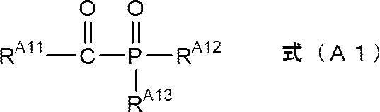
上記式(A1)中、RA11は、置換基を有してもよい炭化水素基を表す。炭化水素基としては特に制限されないが、具体例としては、脂肪族炭化水素基、芳香族炭化水素基などが挙げられ、なかでも、芳香族炭化水素基であることが好ましい。
上記脂肪族炭化水素基は、直鎖状、分岐鎖状、環状のいずれであってもよい。上記脂肪族炭化水素基の具体例としては、直鎖状または分岐状のアルキル基(特に、炭素数1~20)、直鎖状または分岐状のアルケニル基(特に、炭素数2~20)、直鎖状または分岐状のアルキニル基(特に、炭素数2~20)などが挙げられる。上記脂肪族炭化水素基は、直鎖状または分岐状のアルキル基であることが好ましい。
上記芳香族炭化水素基としては、例えば、アリール基、ナフチル基などが挙げられる。上記アリール基としては、例えば、フェニル基、トリル基、キシリル基などの炭素数6~18のアリール基などが挙げられる。
炭化水素基が有してもよい置換基としては特に制限されないが、具体例としては、脂肪族炭化水素基、芳香族炭化水素基、ハロゲン原子(フッ素原子、塩素原子、臭素原子など)などが挙げられる。脂肪族炭化水素基および芳香族炭化水素基の具体例および好適な態様は、上述のとおりである。置換基は、脂肪族炭化水素基であることが好ましい。
上記脂肪族炭化水素基は、直鎖状、分岐鎖状、環状のいずれであってもよい。上記脂肪族炭化水素基の具体例としては、直鎖状または分岐状のアルキル基(特に、炭素数1~20)、直鎖状または分岐状のアルケニル基(特に、炭素数2~20)、直鎖状または分岐状のアルキニル基(特に、炭素数2~20)などが挙げられる。上記脂肪族炭化水素基は、直鎖状または分岐状のアルキル基であることが好ましい。
上記芳香族炭化水素基としては、例えば、アリール基、ナフチル基などが挙げられる。上記アリール基としては、例えば、フェニル基、トリル基、キシリル基などの炭素数6~18のアリール基などが挙げられる。
炭化水素基が有してもよい置換基としては特に制限されないが、具体例としては、脂肪族炭化水素基、芳香族炭化水素基、ハロゲン原子(フッ素原子、塩素原子、臭素原子など)などが挙げられる。脂肪族炭化水素基および芳香族炭化水素基の具体例および好適な態様は、上述のとおりである。置換基は、脂肪族炭化水素基であることが好ましい。
上記式(A1)中、RA12およびRA13は、それぞれ独立に、置換基を有してもよい炭化水素基または炭化水素オキシ基(-OR:ここでRは炭化水素基を表す)を表す。置換基を有してもよい炭化水素基の炭化水素基、および、炭化水素オキシ基の炭化水素基(R)の具体例は上述した炭化水素基と同じである。また、炭化水素基または炭化水素オキシ基が有してもよい置換基の具体例および好適な態様は、上述した置換基と同じである。
RA12とRA13のうち一方は置換基を有してもよい芳香族炭化水素基であることが好ましい。RA12とRA13のうち一方が置換基を有してもよい芳香族炭化水素基である場合、他方は置換基を有してもよいフェニル基(特に炭素数6~18)またはアルコキシ基(特に炭素数1~5のもの)であることが好ましく、置換基を有してもよいフェニル基(特に炭素数6~18)であることがより好ましい。
RA12とRA13のうち一方は置換基を有してもよい芳香族炭化水素基であることが好ましい。RA12とRA13のうち一方が置換基を有してもよい芳香族炭化水素基である場合、他方は置換基を有してもよいフェニル基(特に炭素数6~18)またはアルコキシ基(特に炭素数1~5のもの)であることが好ましく、置換基を有してもよいフェニル基(特に炭素数6~18)であることがより好ましい。
モノアシルホスフィンオキサイド(A1)の具体例としては、ベンゾイル-ジフェニルホスフィンオキサイド、2,4,6-トリメチルベンゾイル-ジフェニルホスフィンオキサイド、2,3,5,6-テトラメチルベンゾイル-ジフェニルホスフィンオキサイド、3,4-ジメチルベンゾイル-ジフェニルホスフィンオキサイド、2,4,6-トリメチルベンゾイル-フェニルエトキシホスフィンオキサイドなどが挙げられる。
モノアシルホスフィンオキサイド(A1)の0.1質量%アセトニトリル溶液の400nmにおける吸光度は1.5以下であることが好ましく、1.3以下であることがより好ましい。モノアシルホスフィンオキサイド(A1)の吸光度の下限は特に制限されないが、0.2以上であることが好ましく、0.3以上であることがより好ましい。
本発明の組成物の全量に対するモノアシルホスフィンオキサイド(A1)の含有量は1.5質量%以上である。なかでも、1.5~3.9質量%であることが好ましい。なお、本明細書において、本発明の組成物が溶媒を含有する場合、本発明の組成物の全量とは溶媒以外の成分の合計の量を指す。
本発明の組成物の全量に対するモノアシルホスフィンオキサイド(A1)の含有量が1.5質量%を下回ると、光による硬化性が低下し、得られる粘着シートの密着性が不十分になる。
本発明の組成物の全量に対するモノアシルホスフィンオキサイド(A1)の含有量が1.5質量%を下回ると、光による硬化性が低下し、得られる粘着シートの密着性が不十分になる。
<ビスアシルホスフィンオキサイド(A2)>
本発明の組成物に含有されるビスアシルホスフィンオキサイド(A2)は特に制限されず、公知のビスアシルホスフィンオキサイドを使用することができる。本発明の組成物は2種以上のビスアシルホスフィンオキサイドを含有しても構わない。
ビスアシルホスフィンオキサイド(A2)の好適な態様としては、例えば、下記式(A2)で表されるビスアシルホスフィンオキサイドが挙げられる。
本発明の組成物に含有されるビスアシルホスフィンオキサイド(A2)は特に制限されず、公知のビスアシルホスフィンオキサイドを使用することができる。本発明の組成物は2種以上のビスアシルホスフィンオキサイドを含有しても構わない。
ビスアシルホスフィンオキサイド(A2)の好適な態様としては、例えば、下記式(A2)で表されるビスアシルホスフィンオキサイドが挙げられる。
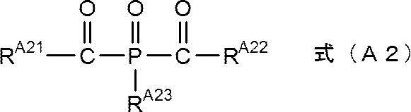
上記式(A2)中、RA21~RA23は、それぞれ独立に、置換基を有してもよい炭化水素基を表す。炭化水素基および置換基の具体例および好適な態様は上述したRA11と同じである。
ビスアシルホスフィンオキサイド(A2)の具体例としては、ビス(2,4,6-トリメチルベンゾイル)-フェニルホスフィンオキサイド、ビス(2,6-ジメトキシベンゾイル)-2,4,4-トリメチル-ペンチルホスフィンオキサイド、ビス(2,6-ジメチルベンゾイル)-エチルホスフィンオキサイドなどが挙げられる。
ビスアシルホスフィンオキサイド(A2)の0.1質量%アセトニトリル溶液の430nmにおける吸光度は0.1以上であることが好ましく、0.2以上であることがより好ましい。ビスアシルホスフィンオキサイド(A2)の吸光度の上限は特に制限されないが、0.8以下であることが好ましく、0.4以下であることがより好ましい。
本発明の組成物の全量に対するビスアシルホスフィンオキサイド(A2)の含有量は特に制限されないが、0.1~2.5質量%であることが好ましい。
ビスアシルホスフィンオキサイド(A2)の含有量(a2)と上記モノアシルホスフィンオキサイド(A1)の含有量(a1)との質量比(a2/a1)は特に制限されないが、得られる粘着シートの密着性および段差追従性がより優れる理由から、0.30以上であることが好ましく、0.40以上であることがより好ましい。
<ラジカル重合性モノマー(B)>
本発明の組成物は、「溶解度パラメータ(SP値)が8.0~10.0であり、かつ、分岐状アルキル基および脂環式炭化水素基(ただし、不飽和炭化水素基を有する脂環式炭化水素基を除く)からなる群より選択される少なくとも1種の基を有するラジカル重合性モノマー(B)」を含有する。本発明の組成物は2種以上のラジカル重合性モノマー(B)を含有しても構わない。
本発明の組成物は、「溶解度パラメータ(SP値)が8.0~10.0であり、かつ、分岐状アルキル基および脂環式炭化水素基(ただし、不飽和炭化水素基を有する脂環式炭化水素基を除く)からなる群より選択される少なくとも1種の基を有するラジカル重合性モノマー(B)」を含有する。本発明の組成物は2種以上のラジカル重合性モノマー(B)を含有しても構わない。
ラジカル重合性モノマー(B)はラジカル重合性基を有する。ラジカル重合性基としては特に制限されないが、例えば、(メタ)アクリロイル基、イタコン酸エステル基、クロトン酸エステル基、イソクロトン酸エステル基、マレイン酸エステル基、スチリル基、ビニル基、アクリルアミド基、メタクリルアミド基などが挙げられる。なかでも、(メタ)アクリロイル基、ビニル基、スチリル基、アクリルアミド基、メタクリルアミド基が好ましく、(メタ)アクリロイル基、スチリル基がより好ましい。
また、上述のとおり、ラジカル重合性モノマー(B)は、分岐状アルキル基および脂環式炭化水素基(ただし、不飽和炭化水素基を有する脂環式炭化水素基を除く)からなる群より選択される少なくとも1種の基を有する。
分岐状アルキル基としては特に制限されないが、炭素数3~30のものが好ましく、5~20のものがより好ましい。分岐状アルキル基の具体例としては、iso-プロピル基、iso-ブチル基、sec-ブチル基、tert-ブチル基、2-エチルヘキシルアルキル基などが挙げられる。
脂環式炭化水素基としては特に制限されないが、炭素数3~30のものが好ましく、5~20のものがより好ましい。脂環式炭化水素基は、単環型であっても、多環型であってもよい。単環型の具体例としては、シクロペンチル基、シクロヘキシル基などが挙げられる。多環型の具体例としては、イソボルニル基、アダマンチル基などが挙げられる。なお、脂環式炭化水素基は不飽和炭化水素基を有するものではない。脂環式炭化水素基が不飽和炭化水素基を有する場合、上述したビスアシルホスフィンオキサイド(A2)との相溶性が低下し、調製が困難となる。不飽和炭化水素基を有する脂環式炭化水素基としては、例えば、ジシクロペンテニル基などが挙げられる。
分岐状アルキル基としては特に制限されないが、炭素数3~30のものが好ましく、5~20のものがより好ましい。分岐状アルキル基の具体例としては、iso-プロピル基、iso-ブチル基、sec-ブチル基、tert-ブチル基、2-エチルヘキシルアルキル基などが挙げられる。
脂環式炭化水素基としては特に制限されないが、炭素数3~30のものが好ましく、5~20のものがより好ましい。脂環式炭化水素基は、単環型であっても、多環型であってもよい。単環型の具体例としては、シクロペンチル基、シクロヘキシル基などが挙げられる。多環型の具体例としては、イソボルニル基、アダマンチル基などが挙げられる。なお、脂環式炭化水素基は不飽和炭化水素基を有するものではない。脂環式炭化水素基が不飽和炭化水素基を有する場合、上述したビスアシルホスフィンオキサイド(A2)との相溶性が低下し、調製が困難となる。不飽和炭化水素基を有する脂環式炭化水素基としては、例えば、ジシクロペンテニル基などが挙げられる。
上述のとおり、ラジカル重合性モノマー(B)のSP値は8.0~10.0である。ここでSP値は、Michael M. Collman, John F. Graf, Paul C. Painter (Pensylvania State Univ.)による、”Specific Interactions and the Miscibility of Polymer Blends” (1991), Technomic Publishing Co. Inc.に記載されている計算で求められる値である。但し、‐COOH基と‐OH基については記載がないため、R. F. FedorsによるPolymer Engineering and Science, 14(2), 147(1974)に記載の値を用いる。SP値が8.0~10.0の範囲を外れた場合、上述したビスアシルホスフィンオキサイド(A2)との相溶性が低下し、調製が困難となる。なお、本明細書においてSP値の単位は(J/cm3)1/2である。
ラジカル重合性モノマー(B)の好適な態様としては、例えば、溶解度パラメータ(SP値)が8.0~10.0であり、かつ、下記式(B1)で表される化合物が挙げられる。

上記式(B1)中、RB11は、水素原子またはアルキル基(好ましくはメチル基)を表す。
上記式(B1)中、LB1は、単結合または2価の有機基を表す。2価の有機基としては特に制限されないが、例えば、2価の脂肪族炭化水素基(例えば、アルキレン基。好ましくは炭素数1~8)、2価の芳香族炭化水素基(例えば、アリーレン基。好ましくは炭素数6~12)、-O-、-S-、-SO2-、-N(R)-(R:アルキル基)、-CO-、-NH-、-COO-、-CONH-、またはこれらを組み合わせた基(例えば、アルキレンオキシ基、アルキレンオキシカルボニル基、アルキレンカルボニルオキシ基など)などが挙げられる。なかでも、アルキレン基、-O-またはこれらを組み合わせた基であることが好ましい。
上記式(B1)中、RB12は、分岐状アルキル基または脂環式炭化水素基(ただし、不飽和炭化水素基を有する脂環式炭化水素基を除く)を表す。分岐状アルキル基および脂環式炭化水素基(ただし、不飽和炭化水素基を有する脂環式炭化水素基を除く)の具体例および好適な態様は上述のとおりである。
ラジカル重合性モノマー(B)の具体例としては、2-エチルヘキシルメタクリレート(SP値:8.1)、シクロヘキシルアクリレート(SP値:8.3)、イソボルニルアクリレート(SP値:8.33)、イソボルニルメタクリレート(SP値:8.3)などが挙げられる。
本発明の組成物の全量に対するラジカル重合性モノマー(B)の含有量は特に制限されないが、1~50質量%であることが好ましく、5~30質量%であることがより好ましい。
ラジカル重合性モノマー(B)の含有量(b)と、上記モノアシルホスフィンオキサイド(A1)および上記ビスアシルホスフィンオキサイド(A2)の合計の含有量(a)との質量比(b/a)は、3.0~30.0である。質量比(b/a)は、得られる粘着シートの密着性および段差追従性がより優れる理由から、4.0以上であることが好ましく、6.0以上であることがより好ましい。
質量比(b/a)が3.0~30.0の範囲から外れると、粘着シートを形成することができるような均質な組成物が得られないか、均質な組成物が得られても密着性が不十分となる。
質量比(b/a)が3.0~30.0の範囲から外れると、粘着シートを形成することができるような均質な組成物が得られないか、均質な組成物が得られても密着性が不十分となる。
<任意成分>
本発明の組成物には、必要に応じて、その効果や目的を損なわない範囲で、上述した成分以外の成分(任意成分)が含有されていてもよい。
任意成分としては、例えば、上述したラジカル重合性モノマー(B)以外のラジカル重合性モノマー、上述したモノアシルホスフィンオキサイド(A1)および上述ビスアシルホスフィンオキサイド(A2)以外の光重合開始剤、増感色素、重合阻害抑制剤、樹脂成分、溶媒などが挙げられる。
本発明の組成物には、必要に応じて、その効果や目的を損なわない範囲で、上述した成分以外の成分(任意成分)が含有されていてもよい。
任意成分としては、例えば、上述したラジカル重合性モノマー(B)以外のラジカル重合性モノマー、上述したモノアシルホスフィンオキサイド(A1)および上述ビスアシルホスフィンオキサイド(A2)以外の光重合開始剤、増感色素、重合阻害抑制剤、樹脂成分、溶媒などが挙げられる。
(ラジカル重合性モノマー(B)以外のラジカル重合性モノマー(M))
ラジカル重合性モノマー(M)としてはラジカル重合性モノマー(B)以外のラジカル重合性モノマーであれば特に制限されないが、例えば、ラジカル重合性基を有する化合物のうちSP値が8.0~10.0の範囲から外れるものや、ラジカル重合性基を有する化合物のうち分岐状アルキル基および脂環式炭化水素基(ただし、不飽和炭化水素基を有する脂環式炭化水素基を除く)を有さないものなどが挙げられる。ラジカル重合性基の具体例は上述したラジカル重合性モノマー(B)と同じである。
ラジカル重合性モノマー(M)としてはラジカル重合性モノマー(B)以外のラジカル重合性モノマーであれば特に制限されないが、例えば、ラジカル重合性基を有する化合物のうちSP値が8.0~10.0の範囲から外れるものや、ラジカル重合性基を有する化合物のうち分岐状アルキル基および脂環式炭化水素基(ただし、不飽和炭化水素基を有する脂環式炭化水素基を除く)を有さないものなどが挙げられる。ラジカル重合性基の具体例は上述したラジカル重合性モノマー(B)と同じである。
ラジカル重合性モノマー(M)の具体例としては、メチル(メタ)アクリレート、2-ヒドロキシルエチル(メタ)アクリレート、ジシクロペンテニルオキシエチル(メタ)アクリレート、2-エチルヘキシルアクリレート(SP値:7.8)などが挙げられる。
本発明の組成物の全量に対するラジカル重合性モノマー(M)の含有量は特に制限されないが、1~20質量%であることが好ましい。
(モノアシルホスフィンオキサイド(A1)およびビスアシルホスフィンオキサイド(A2)以外の光重合開始剤(P))
光重合開始剤(P)としてはモノアシルホスフィンオキサイド(A1)およびビスアシルホスフィンオキサイド(A2)以外の光重合開始剤であれば特に制限されない。
そのような光重合開始剤としては、例えば、2-ベンジル-2-ジメチルアミノ-1-(4-モルフォリノフェニル)ブタノン-1(Irgacure369、BASF社製)などのアミノケトン系光重合開始剤;ヒドロキシシクロヘキシルフェニルケトン(Irgacure184)、ヒドロキシ-2-メチル-1-フェニル-プロパン-1-オン(Darocure1173)などのヒドロキシケトン系光重合開始剤;ベンゾフェノン、2,4,6-トリメチルベンゾフェノン、4-メチルベンゾフェノンなどのベンゾフェノン系光重合開始剤;ベンジルメチルケタール(EsacureKB1、日本シーベルヘグナー社製);2-ヒドロキシ-2-メチル-[4-(1-メチルビニル)フェニル]プロパノールオリゴマー(EsacureKIP150、日本シーベルヘグナー社製)などが挙げられる。
本発明の組成物は、アミノケトン系光重合開始剤およびヒドロキシケトン系光重合開始剤からなる群より選択される少なくとも1種の光重合開始剤を含有するのが好ましい。
光重合開始剤(P)としてはモノアシルホスフィンオキサイド(A1)およびビスアシルホスフィンオキサイド(A2)以外の光重合開始剤であれば特に制限されない。
そのような光重合開始剤としては、例えば、2-ベンジル-2-ジメチルアミノ-1-(4-モルフォリノフェニル)ブタノン-1(Irgacure369、BASF社製)などのアミノケトン系光重合開始剤;ヒドロキシシクロヘキシルフェニルケトン(Irgacure184)、ヒドロキシ-2-メチル-1-フェニル-プロパン-1-オン(Darocure1173)などのヒドロキシケトン系光重合開始剤;ベンゾフェノン、2,4,6-トリメチルベンゾフェノン、4-メチルベンゾフェノンなどのベンゾフェノン系光重合開始剤;ベンジルメチルケタール(EsacureKB1、日本シーベルヘグナー社製);2-ヒドロキシ-2-メチル-[4-(1-メチルビニル)フェニル]プロパノールオリゴマー(EsacureKIP150、日本シーベルヘグナー社製)などが挙げられる。
本発明の組成物は、アミノケトン系光重合開始剤およびヒドロキシケトン系光重合開始剤からなる群より選択される少なくとも1種の光重合開始剤を含有するのが好ましい。
本発明の組成物の全量に対する光重合開始剤(P)の含有量は特に制限されないが、0.1~5質量%であることが好ましい。
(増感色素)
増感色素は特に制限されないが、例えば、チオキサントン類、チオクロマノン類、カルバゾール類、キサントン類などが挙げられる。本発明の組成物は2種以上の増感色素を含有しても構わない。
増感色素は特に制限されないが、例えば、チオキサントン類、チオクロマノン類、カルバゾール類、キサントン類などが挙げられる。本発明の組成物は2種以上の増感色素を含有しても構わない。
増感色素の好適な態様としては、例えば、下記一般式(I)で表される増感色素が挙げられる。

上記一般式(I)中、R11~R18は、それぞれ独立に、水素原子、アルキル基、ハロゲン原子、ヒドロキシ基、シアノ基、ニトロ基、アミノ基、アルキルチオ基、アルキルアミノ基、アルコキシ基、アルコキシカルボニル基、アシルオキシ基、アシル基、カルボキシル基またはスルホ基を表す。R15またはR16と、R17またはR18とは、互いに縮合して5~6員の脂肪族環、芳香族環、または複素環を形成していてもよい。
R11~R14は、それぞれ独立に、水素原子またはハロゲン原子であることが好ましい。R15~R18は、それぞれ独立に、水素原子またはアルキル基であることが好ましい。
R11~R14は、それぞれ独立に、水素原子またはハロゲン原子であることが好ましい。R15~R18は、それぞれ独立に、水素原子またはアルキル基であることが好ましい。
本発明の組成物は、上記一般式(I)で表される増感色素を含有するのが好ましい。
本発明の組成物の全量に対する増感色素の含有量は特に制限されないが、0.1~2質量%であることが好ましい。
(重合阻害抑制剤)
重合阻害抑制剤は、酸素による重合阻害を抑制する働きを有する。重合阻害抑制は特に制限されないが、例えば、亜リン酸エステル(例えば、亜リン酸トリフェニルなど)、アミン(例えば、アニリン、ヒンダードアミン、DBU(ジアザビシクロウンデセン)など)、チオール(例えば、ドデカンチオール、ペンタエリトリトールテトラ(3-メルカプトプロピオナート)など)などが挙げられる。本発明の組成物は2種以上の重合阻害抑制剤を含有しても構わない。
本発明の組成物は、亜リン酸エステル、アミンおよびチオールからなる群より選択される少なくとも1種の重合阻害抑制剤を含有するのが好ましい。
重合阻害抑制剤は、酸素による重合阻害を抑制する働きを有する。重合阻害抑制は特に制限されないが、例えば、亜リン酸エステル(例えば、亜リン酸トリフェニルなど)、アミン(例えば、アニリン、ヒンダードアミン、DBU(ジアザビシクロウンデセン)など)、チオール(例えば、ドデカンチオール、ペンタエリトリトールテトラ(3-メルカプトプロピオナート)など)などが挙げられる。本発明の組成物は2種以上の重合阻害抑制剤を含有しても構わない。
本発明の組成物は、亜リン酸エステル、アミンおよびチオールからなる群より選択される少なくとも1種の重合阻害抑制剤を含有するのが好ましい。
本発明の組成物の全量に対する重合阻害抑制剤の含有量は特に制限されないが、0.1~1.0質量%であることが好ましい。
(樹脂成分)
本発明の組成物は樹脂成分を含有するのが好ましい。樹脂成分としては特に制限されないが、ジエン系ゴム(例えば、液状ポリブタジエンなどの液状ゴム)、石油系樹脂(例えば、芳香族系石油樹脂、脂肪族系石油樹脂、C9留分による樹脂など)、テルペン樹脂(例えば、水添テルペン樹脂、芳香族変性テルペン樹脂)、ロジン系樹脂(例えば、部分水素化ガムロジン樹脂、エリトリトール変性木材ロジン樹脂、トール油ロジン樹脂、ウッドロジン樹脂)、クマロンインデン系樹脂(例えば、クロマンインデンスチレン共重合体)、スチレン系樹脂(例えば、ポリスチレン、スチレンとα-メチルスチレンの共重合体等)などの粘着付与剤が挙げられる。なかでも、液状ゴム、テルペン樹脂が好ましい。
本発明の組成物がテルペン樹脂を含有する場合、本発明の組成物の全量に対するテルペン樹脂の含有量は特に制限されないが、10~50質量%であることが好ましい。
本発明の組成物が液状ゴムを含有する場合、本発明の組成物の全量に対する液状ゴムの含有量は特に制限されないが、10~50質量%であることが好ましい。
本発明の組成物は樹脂成分を含有するのが好ましい。樹脂成分としては特に制限されないが、ジエン系ゴム(例えば、液状ポリブタジエンなどの液状ゴム)、石油系樹脂(例えば、芳香族系石油樹脂、脂肪族系石油樹脂、C9留分による樹脂など)、テルペン樹脂(例えば、水添テルペン樹脂、芳香族変性テルペン樹脂)、ロジン系樹脂(例えば、部分水素化ガムロジン樹脂、エリトリトール変性木材ロジン樹脂、トール油ロジン樹脂、ウッドロジン樹脂)、クマロンインデン系樹脂(例えば、クロマンインデンスチレン共重合体)、スチレン系樹脂(例えば、ポリスチレン、スチレンとα-メチルスチレンの共重合体等)などの粘着付与剤が挙げられる。なかでも、液状ゴム、テルペン樹脂が好ましい。
本発明の組成物がテルペン樹脂を含有する場合、本発明の組成物の全量に対するテルペン樹脂の含有量は特に制限されないが、10~50質量%であることが好ましい。
本発明の組成物が液状ゴムを含有する場合、本発明の組成物の全量に対する液状ゴムの含有量は特に制限されないが、10~50質量%であることが好ましい。
(溶媒)
本発明の組成物には、必要に応じて、溶媒が含有されていてもよい。使用される溶媒としては、例えば、水、有機溶媒(例えば、メタノール等のアルコール類、アセトン等のケトン類、ホルムアミド等のアミド類、ジメチルスルホキシド等のスルホキシド類、酢酸エチル等のエステル類、エーテル類等)、またはこれらの混合溶媒を挙げることができる。
本発明の組成物には、必要に応じて、溶媒が含有されていてもよい。使用される溶媒としては、例えば、水、有機溶媒(例えば、メタノール等のアルコール類、アセトン等のケトン類、ホルムアミド等のアミド類、ジメチルスルホキシド等のスルホキシド類、酢酸エチル等のエステル類、エーテル類等)、またはこれらの混合溶媒を挙げることができる。
本発明の組成物には、上記以外にも、表面潤滑剤、レベリング剤、酸化防止剤、腐食防止剤、光安定剤、紫外線吸収剤、重合禁止剤、シランカップリング剤、無機または有機の充填剤、金属粉、顔料などの粉体、粒子状、箔状物などの従来公知の各種の添加剤を使用する用途に応じて適宜添加することができる。
<粘着剤組成物に含まれる酸素原子のモル数と炭素原子のモル数との比>
本発明の組成物中の酸素原子のモル数と炭素原子のモル数との比(酸素原子のモル数/炭素原子のモル数)(以下、「O/C比」とも言う)は0.1以下である。なかでも、0.005~0.05であることが好ましい。
O/C比が0.1を超える場合、粘着シートとして静電容量式タッチパネルに用いたときに誤動作が発生しやすくなる。
なお、本発明の組成物が溶媒を含有する場合、O/C比は、溶媒以外の全ての成分中のO/C比を指す。
本発明の組成物中の酸素原子のモル数と炭素原子のモル数との比(酸素原子のモル数/炭素原子のモル数)(以下、「O/C比」とも言う)は0.1以下である。なかでも、0.005~0.05であることが好ましい。
O/C比が0.1を超える場合、粘着シートとして静電容量式タッチパネルに用いたときに誤動作が発生しやすくなる。
なお、本発明の組成物が溶媒を含有する場合、O/C比は、溶媒以外の全ての成分中のO/C比を指す。
上記O/C比は、粘着剤組成物中の各成分について酸素原子のモル数と炭素原子のモル数を計算することで求めることができる。
例えば、粘着剤組成物が、モノアシルホスフィンオキサイド(A1)とビスアシルホスフィンオキサイド(A2)とラジカル重合性モノマー(B)とテルペン樹脂と液状ゴムとを含有する場合、O/C比は、[モノアシルホスフィンオキサイド(A1)の酸素原子のモル数+ビスアシルホスフィンオキサイド(A2)の酸素原子のモル数+ラジカル重合性モノマー(B)の酸素原子のモル数+テルペン樹脂の酸素原子のモル数+液状ゴムの酸素原子のモル数]/[モノアシルホスフィンオキサイド(A1)の炭素原子のモル数+ビスアシルホスフィンオキサイド(A2)の炭素原子のモル数+ラジカル重合性モノマー(B)の炭素原子のモル数+テルペン樹脂の液状ゴムの炭素原子のモル数]により求めることができる。
例えば、粘着剤組成物が、モノアシルホスフィンオキサイド(A1)とビスアシルホスフィンオキサイド(A2)とラジカル重合性モノマー(B)とテルペン樹脂と液状ゴムとを含有する場合、O/C比は、[モノアシルホスフィンオキサイド(A1)の酸素原子のモル数+ビスアシルホスフィンオキサイド(A2)の酸素原子のモル数+ラジカル重合性モノマー(B)の酸素原子のモル数+テルペン樹脂の酸素原子のモル数+液状ゴムの酸素原子のモル数]/[モノアシルホスフィンオキサイド(A1)の炭素原子のモル数+ビスアシルホスフィンオキサイド(A2)の炭素原子のモル数+ラジカル重合性モノマー(B)の炭素原子のモル数+テルペン樹脂の液状ゴムの炭素原子のモル数]により求めることができる。
<粘着剤組成物の調製方法>
本発明の組成物の調製方法は特に制限されず、公知の方法を採用できる。例えば、上記各成分を混合した後、公知の手段により撹拌することによって調製することができる。
本発明の組成物の調製方法は特に制限されず、公知の方法を採用できる。例えば、上記各成分を混合した後、公知の手段により撹拌することによって調製することができる。
[粘着シート]
本発明の粘着シートは、上述した本発明の組成物から得られる粘着シートである。
粘着シートの厚みは特に制限されないが、5~2500μmであることが好ましく、50~500μmであることがより好ましく、100~250μmであることがさらに好ましい。
粘着シートは、光学的に透明であることが好ましい。つまり、透明粘着シートであることが好ましい。光学的に透明とは、全光線透過率は85%以上であることを意図し、90%以上が好ましく、95%以上がより好ましい。
本発明の粘着シートは、上述した本発明の組成物から得られる粘着シートである。
粘着シートの厚みは特に制限されないが、5~2500μmであることが好ましく、50~500μmであることがより好ましく、100~250μmであることがさらに好ましい。
粘着シートは、光学的に透明であることが好ましい。つまり、透明粘着シートであることが好ましい。光学的に透明とは、全光線透過率は85%以上であることを意図し、90%以上が好ましく、95%以上がより好ましい。
<粘着シートの作製方法>
粘着シートの製造方法は特に制限されず、公知の方法より製造できる。例えば、上述した本発明の組成物を所定の基材(例えば、離型PETなどの離型シート)上に塗布し、光(紫外線、可視光線、X線など)照射することで硬化させる方法が挙げられる。
組成物を塗布する方法としては、例えば、グラビアコーター、コンマコーター、バーコーター、ナイフコーター、ダイコーター、ロールコーターなどによる方法が挙げられる。
光照射する方法としては、例えば、低圧水銀灯、中圧水銀灯、高圧水銀灯、メタルハライドランプ、Deep-UV光、キセノンランプ、ケミカルランプ、カーボンアーク灯などによる方法が挙げられる。光照射のエネルギーは特に制限されないが、1~10J/cm2であるのが好ましい。
粘着シートの形成後、必要に応じて、形成された粘着シートの露出した表面上に離型PETなどの離型シートを積層してもよい。
粘着シートの製造方法は特に制限されず、公知の方法より製造できる。例えば、上述した本発明の組成物を所定の基材(例えば、離型PETなどの離型シート)上に塗布し、光(紫外線、可視光線、X線など)照射することで硬化させる方法が挙げられる。
組成物を塗布する方法としては、例えば、グラビアコーター、コンマコーター、バーコーター、ナイフコーター、ダイコーター、ロールコーターなどによる方法が挙げられる。
光照射する方法としては、例えば、低圧水銀灯、中圧水銀灯、高圧水銀灯、メタルハライドランプ、Deep-UV光、キセノンランプ、ケミカルランプ、カーボンアーク灯などによる方法が挙げられる。光照射のエネルギーは特に制限されないが、1~10J/cm2であるのが好ましい。
粘着シートの形成後、必要に応じて、形成された粘着シートの露出した表面上に離型PETなどの離型シートを積層してもよい。
なお、粘着シートは、基材を有しないタイプ(基材レス粘着シート)であっても、基材の少なくとも一方の主面に粘着層が配置された基材を有するタイプ(基材付き粘着シート。例えば、基材の両面に粘着層を有する基材付き両面粘着シート、基材の片面にのみ粘着層を有する基材付き片面粘着シート)であってもよい。
[タッチパネル用積層体、静電容量式タッチパネル]
本発明のタッチパネル用積層体は、上述した本発明の粘着シートと、静電容量式タッチパネルセンサーとを備える。
本発明のタッチパネル用積層体の一態様について図面を参照して説明する。
図1は、本発明のタッチパネル用積層体の一態様を模式的に表す断面図である。図1において、タッチパネル用積層体100は、粘着シート12と、静電容量式タッチパネルセンサー18とを備える。
また、図2は、本発明のタッチパネル用積層体の別の態様を模式的に表す断面図である。図2において、タッチパネル用積層体200は、保護基板20と、粘着シート12と、静電容量式タッチパネルセンサー18とを備える。
本発明のタッチパネル用積層体は、上述した本発明の粘着シートと、静電容量式タッチパネルセンサーとを備える。
本発明のタッチパネル用積層体の一態様について図面を参照して説明する。
図1は、本発明のタッチパネル用積層体の一態様を模式的に表す断面図である。図1において、タッチパネル用積層体100は、粘着シート12と、静電容量式タッチパネルセンサー18とを備える。
また、図2は、本発明のタッチパネル用積層体の別の態様を模式的に表す断面図である。図2において、タッチパネル用積層体200は、保護基板20と、粘着シート12と、静電容量式タッチパネルセンサー18とを備える。
また、本発明の静電容量式タッチパネルは、静電容量式タッチパネルセンサーと、上述した本発明の粘着シートと、表示装置とをこの順に備える。
本発明の静電容量式タッチパネルの一態様について図面を参照して説明する。
図3(A)は、本発明の静電容量式タッチパネルの一態様を模式的に表す断面図である。図3(A)において、静電容量式タッチパネル300は、静電容量式タッチパネルセンサー18と、粘着シート12と、表示装置50とを備える。
また、図3(B)は、本発明の静電容量式タッチパネルの別の態様を模式的に表す断面図である。図3(B)において、静電容量式タッチパネル400は、保護基板20と、粘着シート12と、静電容量式タッチパネルセンサー18と、粘着シート12と、表示装置50とを備える。
また、図3(C)は、本発明の静電容量式タッチパネルのさらに別の態様を模式的に表す断面図である。図3(C)において、静電容量式タッチパネル500は、保護基板一体型静電容量式タッチパネルセンサー60と、粘着シート12と、表示装置50とを備える。ここで、保護基板一体型静電容量式タッチパネルセンサー60は、後述するように、保護基板と静電容量式タッチパネルセンサーとが一体となった部材であり、保護基板と静電容量式タッチパネルセンサーとの間に粘着シートを備えない。そのため、保護基板一体型静電容量式タッチパネルセンサー60を備える静電容量式タッチパネル500は、上述した静電容量式タッチパネル400と比較して、厚みが薄くなる。
以下、タッチパネル用積層体および静電容量式タッチパネルで使用される各種部材について詳述する。
本発明の静電容量式タッチパネルの一態様について図面を参照して説明する。
図3(A)は、本発明の静電容量式タッチパネルの一態様を模式的に表す断面図である。図3(A)において、静電容量式タッチパネル300は、静電容量式タッチパネルセンサー18と、粘着シート12と、表示装置50とを備える。
また、図3(B)は、本発明の静電容量式タッチパネルの別の態様を模式的に表す断面図である。図3(B)において、静電容量式タッチパネル400は、保護基板20と、粘着シート12と、静電容量式タッチパネルセンサー18と、粘着シート12と、表示装置50とを備える。
また、図3(C)は、本発明の静電容量式タッチパネルのさらに別の態様を模式的に表す断面図である。図3(C)において、静電容量式タッチパネル500は、保護基板一体型静電容量式タッチパネルセンサー60と、粘着シート12と、表示装置50とを備える。ここで、保護基板一体型静電容量式タッチパネルセンサー60は、後述するように、保護基板と静電容量式タッチパネルセンサーとが一体となった部材であり、保護基板と静電容量式タッチパネルセンサーとの間に粘着シートを備えない。そのため、保護基板一体型静電容量式タッチパネルセンサー60を備える静電容量式タッチパネル500は、上述した静電容量式タッチパネル400と比較して、厚みが薄くなる。
以下、タッチパネル用積層体および静電容量式タッチパネルで使用される各種部材について詳述する。
〔静電容量式タッチパネルセンサー〕
静電容量式タッチパネルセンサー18とは、表示装置上(操作者側)に配置され、人間の指などの外部導体が接触(接近)するときに発生する静電容量の変化を利用して、人間の指などの外部導体の位置を検出するセンサーである。
静電容量式タッチパネルセンサー18の構成は特に制限されないが、通常、検出電極(特に、X方向に延びる検出電極およびY方向に延びる検出電極)を有し、指が接触または近接した検出電極の静電容量変化を検出することによって、指の座標を特定する。
静電容量式タッチパネルセンサー18とは、表示装置上(操作者側)に配置され、人間の指などの外部導体が接触(接近)するときに発生する静電容量の変化を利用して、人間の指などの外部導体の位置を検出するセンサーである。
静電容量式タッチパネルセンサー18の構成は特に制限されないが、通常、検出電極(特に、X方向に延びる検出電極およびY方向に延びる検出電極)を有し、指が接触または近接した検出電極の静電容量変化を検出することによって、指の座標を特定する。
図4を用いて、静電容量式タッチパネルセンサー18の好適態様について詳述する。
図4に、静電容量式タッチパネルセンサー180の平面図を示す。図5は、図4中の切断線A-Aに沿って切断した断面図である。静電容量式タッチパネルセンサー180は、基板22と、基板22の一方の主面上(表面上)に配置される第1検出電極24と、第1引き出し配線26と、基板22の他方の主面上(裏面上)に配置される第2検出電極28と、第2引き出し配線30と、フレキシブルプリント配線板32とを備える。なお、第1検出電極24および第2検出電極28がある領域は、使用者によって入力操作が可能な入力領域EI(物体の接触を検知可能な入力領域(センシング部))を構成し、入力領域EIの外側に位置する外側領域EOには第1引き出し配線26、第2引き出し配線30およびフレキシブルプリント配線板32が配置される。
以下では、上記構成について詳述する。
図4に、静電容量式タッチパネルセンサー180の平面図を示す。図5は、図4中の切断線A-Aに沿って切断した断面図である。静電容量式タッチパネルセンサー180は、基板22と、基板22の一方の主面上(表面上)に配置される第1検出電極24と、第1引き出し配線26と、基板22の他方の主面上(裏面上)に配置される第2検出電極28と、第2引き出し配線30と、フレキシブルプリント配線板32とを備える。なお、第1検出電極24および第2検出電極28がある領域は、使用者によって入力操作が可能な入力領域EI(物体の接触を検知可能な入力領域(センシング部))を構成し、入力領域EIの外側に位置する外側領域EOには第1引き出し配線26、第2引き出し配線30およびフレキシブルプリント配線板32が配置される。
以下では、上記構成について詳述する。
基板22は、入力領域EIにおいて第1検出電極24および第2検出電極28を支持する役割を担うと共に、外側領域EOにおいて第1引き出し配線26および第2引き出し配線30を支持する役割を担う部材である。
基板22は、光を適切に透過することが好ましい。具体的には、基板22の全光線透過率は、85~100%であることが好ましい。
基板22は、絶縁性を有する(絶縁基板である)ことが好ましい。つまり、基板22は、第1検出電極24および第2検出電極28の間の絶縁性を担保するための層である。
基板22は、光を適切に透過することが好ましい。具体的には、基板22の全光線透過率は、85~100%であることが好ましい。
基板22は、絶縁性を有する(絶縁基板である)ことが好ましい。つまり、基板22は、第1検出電極24および第2検出電極28の間の絶縁性を担保するための層である。
基板22としては、透明基板(特に、透明絶縁性基板)であることが好ましい。その具体例としては、例えば、絶縁樹脂基板、セラミックス基板、ガラス基板などが挙げられる。なかでも、靭性に優れる理由から、絶縁樹脂基板であることが好ましい。
絶縁樹脂基板を構成する材料としては、より具体的には、ポリエチレンテレフタレート、ポリエーテルスルホン、ポリアクリル系樹脂、ポリウレタン系樹脂、ポリエステル、ポリカーボネート、ポリスルホン、ポリアミド、ポリアリレート、ポリオレフィン、セルロース系樹脂、ポリ塩化ビニル、シクロオレフィン系樹脂などが挙げられる。なかでも、透明性に優れる理由から、ポリエチレンテレフタレート、シクロオレフィン系樹脂、ポリカーボネート、トリアセチルセルロース樹脂であることが好ましい。
絶縁樹脂基板を構成する材料としては、より具体的には、ポリエチレンテレフタレート、ポリエーテルスルホン、ポリアクリル系樹脂、ポリウレタン系樹脂、ポリエステル、ポリカーボネート、ポリスルホン、ポリアミド、ポリアリレート、ポリオレフィン、セルロース系樹脂、ポリ塩化ビニル、シクロオレフィン系樹脂などが挙げられる。なかでも、透明性に優れる理由から、ポリエチレンテレフタレート、シクロオレフィン系樹脂、ポリカーボネート、トリアセチルセルロース樹脂であることが好ましい。
図4において、基板22は単層であるが、2層以上の複層であってもよい。
基板22の厚み(基板22が2層以上の複層の場合は、それらの合計厚み)は特に制限されないが、5~350μmであることが好ましく、30~150μmであることがより好ましい。上記範囲内であれば所望の可視光の透過率が得られ、且つ、取り扱いも容易である。
また、図4においては、基板22の平面視形状は実質的に矩形状とされているが、これには限られない。例えば、円形状、多角形状であってもよい。
基板22の厚み(基板22が2層以上の複層の場合は、それらの合計厚み)は特に制限されないが、5~350μmであることが好ましく、30~150μmであることがより好ましい。上記範囲内であれば所望の可視光の透過率が得られ、且つ、取り扱いも容易である。
また、図4においては、基板22の平面視形状は実質的に矩形状とされているが、これには限られない。例えば、円形状、多角形状であってもよい。
第1検出電極24および第2検出電極28は、静電容量の変化を感知するセンシング電極であり、感知部(センサ部)を構成する。つまり、指先をタッチパネルに接触させると、第1検出電極24および第2検出電極28の間の相互静電容量が変化し、この変化量に基づいて指先の位置をIC回路によって演算する。
第1検出電極24は、入力領域EIに接近した使用者の指のX方向における入力位置の検出を行う役割を有するものであり、指との間に静電容量を発生する機能を有している。第1検出電極24は、第1方向(X方向)に延び、第1方向と直交する第2方向(Y方向)に所定の間隔をあけて配列された電極であり、後述するように所定のパターンを含む。
第2検出電極28は、入力領域EIに接近した使用者の指のY方向における入力位置の検出を行う役割を有するものであり、指との間に静電容量を発生する機能を有している。第2検出電極28は、第2方向(Y方向)に延び、第1方向(X方向)に所定の間隔をあけて配列された電極であり、後述するように所定のパターンを含む。図4においては、第1検出電極24は5つ、第2検出電極28は5つ設けられているが、その数は特に制限されず複数あればよい。
第1検出電極24は、入力領域EIに接近した使用者の指のX方向における入力位置の検出を行う役割を有するものであり、指との間に静電容量を発生する機能を有している。第1検出電極24は、第1方向(X方向)に延び、第1方向と直交する第2方向(Y方向)に所定の間隔をあけて配列された電極であり、後述するように所定のパターンを含む。
第2検出電極28は、入力領域EIに接近した使用者の指のY方向における入力位置の検出を行う役割を有するものであり、指との間に静電容量を発生する機能を有している。第2検出電極28は、第2方向(Y方向)に延び、第1方向(X方向)に所定の間隔をあけて配列された電極であり、後述するように所定のパターンを含む。図4においては、第1検出電極24は5つ、第2検出電極28は5つ設けられているが、その数は特に制限されず複数あればよい。
図4中、第1検出電極24および第2検出電極28は、導電性細線により構成される。図6に、第1検出電極24の一部の拡大平面図を示す。図6に示すように、第1検出電極24は、導電性細線34により構成され、交差する導電性細線34による複数の格子36を含んでいる。なお、第2検出電極28も、第1検出電極24と同様に、交差する導電性細線34による複数の格子36を含んでいる。
導電性細線34の材料としては、例えば、金(Au)、銀(Ag)、銅(Cu)、アルミニウム(Al)などの金属や合金、ITO、酸化スズ、酸化亜鉛、酸化カドミウム、酸化ガリウム、酸化チタンなどの金属酸化物、などが挙げられる。なかでも、導電性細線34の導電性が優れる理由から、銀であることが好ましい。
導電性細線34の中には、導電性細線34と基板22との密着性の観点から、バインダーが含まれていることが好ましい。
バインダーとしては、導電性細線34と基板22との密着性がより優れる理由から、水溶性高分子であることが好ましい。バインダーの種類としては、例えば、ゼラチン、カラギナン、ポリビニルアルコール(PVA)、ポリビニルピロリドン(PVP)、澱粉等の多糖類、セルロースおよびその誘導体、ポリエチレンオキサイド、ポリサッカライド、ポリビニルアミン、キトサン、ポリリジン、ポリアクリル酸、ポリアルギン酸、ポリヒアルロン酸、カルボキシセルロース、アラビアゴム、アルギン酸ナトリウムなどが挙げられる。なかでも、導電性細線34と基板22との密着性がより優れる理由から、ゼラチンが好ましい。
なお、ゼラチンとしては石灰処理ゼラチンの他、酸処理ゼラチンを用いてもよく、ゼラチンの加水分解物、ゼラチン酵素分解物、その他アミノ基、カルボキシル基を修飾したゼラチン(フタル化ゼラチン、アセチル化ゼラチン)を使用することができる。
バインダーとしては、導電性細線34と基板22との密着性がより優れる理由から、水溶性高分子であることが好ましい。バインダーの種類としては、例えば、ゼラチン、カラギナン、ポリビニルアルコール(PVA)、ポリビニルピロリドン(PVP)、澱粉等の多糖類、セルロースおよびその誘導体、ポリエチレンオキサイド、ポリサッカライド、ポリビニルアミン、キトサン、ポリリジン、ポリアクリル酸、ポリアルギン酸、ポリヒアルロン酸、カルボキシセルロース、アラビアゴム、アルギン酸ナトリウムなどが挙げられる。なかでも、導電性細線34と基板22との密着性がより優れる理由から、ゼラチンが好ましい。
なお、ゼラチンとしては石灰処理ゼラチンの他、酸処理ゼラチンを用いてもよく、ゼラチンの加水分解物、ゼラチン酵素分解物、その他アミノ基、カルボキシル基を修飾したゼラチン(フタル化ゼラチン、アセチル化ゼラチン)を使用することができる。
また、バインダーとしては、上記ゼラチンとは異なる高分子(以後、単に高分子とも称する)をゼラチンと共に使用してもよい。
使用される高分子の種類はゼラチンと異なれば特に制限されないが、例えば、アクリル系樹脂、スチレン系樹脂、ビニル系樹脂、ポリオレフィン系樹脂、ポリエステル系樹脂、ポリウレタン系樹脂、ポリアミド系樹脂、ポリカーボネート系樹脂、ポリジエン系樹脂、エポキシ系樹脂、シリコーン系樹脂、セルロース系重合体およびキトサン系重合体、からなる群から選ばれる少なくともいずれかの樹脂、または、これらの樹脂を構成する単量体からなる共重合体などが挙げられる。
使用される高分子の種類はゼラチンと異なれば特に制限されないが、例えば、アクリル系樹脂、スチレン系樹脂、ビニル系樹脂、ポリオレフィン系樹脂、ポリエステル系樹脂、ポリウレタン系樹脂、ポリアミド系樹脂、ポリカーボネート系樹脂、ポリジエン系樹脂、エポキシ系樹脂、シリコーン系樹脂、セルロース系重合体およびキトサン系重合体、からなる群から選ばれる少なくともいずれかの樹脂、または、これらの樹脂を構成する単量体からなる共重合体などが挙げられる。
導電性細線34中における金属とバインダーとの体積比(金属の体積/バインダーの体積)は、1.0以上が好ましく、1.5以上がさらに好ましい。金属とバインダーの体積比を1.0以上とすることで、導電性細線34の導電性をより高めることができる。上限は特に制限されないが、生産性の観点から、6.0以下が好ましく、4.0以下がより好ましく、2.5以下がさらに好ましい。
なお、金属とバインダーの体積比は、導電性細線34中に含まれる金属およびバインダーの密度より計算することができる。例えば、金属が銀の場合、銀の密度を10.5g/cm3として、バインダーがゼラチンの場合、ゼラチンの密度を1.34g/cm3として計算して求めるものとする。
なお、金属とバインダーの体積比は、導電性細線34中に含まれる金属およびバインダーの密度より計算することができる。例えば、金属が銀の場合、銀の密度を10.5g/cm3として、バインダーがゼラチンの場合、ゼラチンの密度を1.34g/cm3として計算して求めるものとする。
導電性細線34の線幅は特に制限されないが、低抵抗の電極を比較的容易に形成できる観点から、30μm以下が好ましく、15μm以下がより好ましく、10μm以下がさらに好ましく、9μm以下が特に好ましく、7μm以下が最も好ましく、0.5μm以上が好ましく、1.0μm以上がより好ましい。
導電性細線34の厚みは特に制限されないが、導電性と視認性との観点から、0.00001mm~0.2mmから選択可能であるが、30μm以下が好ましく、20μm以下がより好ましく、0.01~9μmがさらに好ましく、0.05~5μmが最も好ましい。
導電性細線34の厚みは特に制限されないが、導電性と視認性との観点から、0.00001mm~0.2mmから選択可能であるが、30μm以下が好ましく、20μm以下がより好ましく、0.01~9μmがさらに好ましく、0.05~5μmが最も好ましい。
格子36は、導電性細線34で囲まれる開口領域を含んでいる。格子36の一辺の長さWは、800μm以下が好ましく、600μm以下がより好ましく、400μm以上であることが好ましい。
第1検出電極24および第2検出電極28では、可視光透過率の点から開口率は85%以上であることが好ましく、90%以上であることがより好ましく、95%以上であることが最も好ましい。開口率とは、所定領域において第1検出電極24または第2検出電極28中の導電性細線34を除いた透過性部分が全体に占める割合に相当する。
第1検出電極24および第2検出電極28では、可視光透過率の点から開口率は85%以上であることが好ましく、90%以上であることがより好ましく、95%以上であることが最も好ましい。開口率とは、所定領域において第1検出電極24または第2検出電極28中の導電性細線34を除いた透過性部分が全体に占める割合に相当する。
格子36は、略ひし形の形状を有している。但し、その他、多角形状(例えば、三角形、四角形、六角形)としてもよい。また、一辺の形状を直線状の他、湾曲形状でもよいし、円弧状にしてもよい。円弧状とする場合は、例えば、対向する2辺については、外方に凸の円弧状とし、他の対向する2辺については、内方に凸の円弧状としてもよい。また、各辺の形状を、外方に凸の円弧と内方に凸の円弧が連続した波線形状としてもよい。もちろん、各辺の形状を、サイン曲線にしてもよい。
なお、図6においては、導電性細線34はメッシュパターンとして形成されているが、この態様には限定されず、ストライプパターンであってもよい。
なお、図6においては、導電性細線34はメッシュパターンとして形成されているが、この態様には限定されず、ストライプパターンであってもよい。
第1引き出し配線26および第2引き出し配線30は、それぞれ上記第1検出電極24および第2検出電極28に電圧を印加するための役割を担う部材である。
第1引き出し配線26は、外側領域EOの基板22上に配置され、その一端が対応する第1検出電極24に電気的に接続され、その他端はフレキシブルプリント配線板32に電気的に接続される。
第2引き出し配線30は、外側領域EOの基板22上に配置され、その一端が対応する第2検出電極28に電気的に接続され、その他端はフレキシブルプリント配線板32に電気的に接続される。
なお、図4においては、第1引き出し配線26は5本、第2引き出し配線30は5本記載されているが、その数は特に制限されず、通常、検出電極の数に応じて複数配置される。
第1引き出し配線26は、外側領域EOの基板22上に配置され、その一端が対応する第1検出電極24に電気的に接続され、その他端はフレキシブルプリント配線板32に電気的に接続される。
第2引き出し配線30は、外側領域EOの基板22上に配置され、その一端が対応する第2検出電極28に電気的に接続され、その他端はフレキシブルプリント配線板32に電気的に接続される。
なお、図4においては、第1引き出し配線26は5本、第2引き出し配線30は5本記載されているが、その数は特に制限されず、通常、検出電極の数に応じて複数配置される。
第1引き出し配線26および第2引き出し配線30を構成する材料としては、例えば、金(Au)、銀(Ag)、銅(Cu)などの金属や、酸化スズ、酸化亜鉛、酸化カドミウム、酸化ガリウム、酸化チタンなどの金属酸化物などが挙げられる。なかでも、導電性が優れる理由から、銀であることが好ましい。また、銀ペーストや銅ペーストなどの金属ペーストや、アルミニウム(Al)やモリブデン(Mo)などの金属や合金薄膜で構成されていてもよい。金属ペーストの場合は、スクリーン印刷やインクジェット印刷法で、金属や合金薄膜の場合は、スパッタ膜をフォトリソグラフィー法などのパターニング方法が好適に用いられる。
なお、第1引き出し配線26および第2引き出し配線30中には、基板22との密着性がより優れる点から、バインダーが含まれていることが好ましい。バインダーの種類は、上述の通りである。
なお、第1引き出し配線26および第2引き出し配線30中には、基板22との密着性がより優れる点から、バインダーが含まれていることが好ましい。バインダーの種類は、上述の通りである。
フレキシブルプリント配線板32は、基板上に複数の配線および端子が設けられた板であり、第1引き出し配線26のそれぞれの他端および第2引き出し配線30のそれぞれの他端に接続され、静電容量式タッチパネルセンサー180と外部の装置(例えば、表示装置)とを接続する役割を果たす。
〔静電容量式タッチパネルセンサーの製造方法〕
静電容量式タッチパネルセンサー180の製造方法は特に制限されず、公知の方法を採用することができる。例えば、基板22の両主面上に形成された金属箔上のフォトレジスト膜を露光、現像処理してレジストパターンを形成し、レジストパターンから露出する金属箔をエッチングする方法が挙げられる。また、基板22の両主面上に金属微粒子または金属ナノワイヤを含むペーストを印刷し、ペーストに金属めっきを行う方法が挙げられる。また、基板22上にスクリーン印刷版またはグラビア印刷版によって印刷形成する方法、または、インクジェットにより形成する方法も挙げられる。
静電容量式タッチパネルセンサー180の製造方法は特に制限されず、公知の方法を採用することができる。例えば、基板22の両主面上に形成された金属箔上のフォトレジスト膜を露光、現像処理してレジストパターンを形成し、レジストパターンから露出する金属箔をエッチングする方法が挙げられる。また、基板22の両主面上に金属微粒子または金属ナノワイヤを含むペーストを印刷し、ペーストに金属めっきを行う方法が挙げられる。また、基板22上にスクリーン印刷版またはグラビア印刷版によって印刷形成する方法、または、インクジェットにより形成する方法も挙げられる。
さらに、上記方法以外にハロゲン化銀を使用した方法が挙げられる。より具体的には、基板22の両面にそれぞれ、ハロゲン化銀とバインダーとを含有するハロゲン化銀乳剤層(以後、単に感光性層とも称する)を形成する工程(1)、感光性層を露光した後、現像処理する工程(2)を有する方法が挙げられる。
以下に、各工程に関して説明する。
以下に、各工程に関して説明する。
<工程(1):感光性層形成工程>
工程(1)は、基板22の両面に、ハロゲン化銀とバインダーとを含有する感光性層を形成する工程である。
感光性層を形成する方法は特に制限されないが、生産性の点から、ハロゲン化銀およびバインダーを含有する感光性層形成用組成物を基板22に接触させ、基板22の両面上に感光性層を形成する方法が好ましい。
以下に、上記方法で使用される感光性層形成用組成物の態様について詳述した後、工程の手順について詳述する。
工程(1)は、基板22の両面に、ハロゲン化銀とバインダーとを含有する感光性層を形成する工程である。
感光性層を形成する方法は特に制限されないが、生産性の点から、ハロゲン化銀およびバインダーを含有する感光性層形成用組成物を基板22に接触させ、基板22の両面上に感光性層を形成する方法が好ましい。
以下に、上記方法で使用される感光性層形成用組成物の態様について詳述した後、工程の手順について詳述する。
感光性層形成用組成物には、ハロゲン化銀およびバインダーが含有される。
ハロゲン化銀に含有されるハロゲン元素は、塩素、臭素、ヨウ素およびフッ素のいずれであってもよく、これらを組み合わせでもよい。ハロゲン化銀としては、例えば、塩化銀、臭化銀、ヨウ化銀を主体としたハロゲン化銀が好ましく用いられ、さらに臭化銀や塩化銀を主体としたハロゲン化銀が好ましく用いられる。
使用されるバインダーの種類は、上述の通りである。また、バインダーはラテックスの形態で感光性層形成用組成物中に含まれていてもよい。
感光性層形成用組成物中に含まれるハロゲン化銀およびバインダーの体積比は特に制限されず、上述した導電性細線34中における金属とバインダーとの好適な体積比の範囲となるように適宜調整される。
ハロゲン化銀に含有されるハロゲン元素は、塩素、臭素、ヨウ素およびフッ素のいずれであってもよく、これらを組み合わせでもよい。ハロゲン化銀としては、例えば、塩化銀、臭化銀、ヨウ化銀を主体としたハロゲン化銀が好ましく用いられ、さらに臭化銀や塩化銀を主体としたハロゲン化銀が好ましく用いられる。
使用されるバインダーの種類は、上述の通りである。また、バインダーはラテックスの形態で感光性層形成用組成物中に含まれていてもよい。
感光性層形成用組成物中に含まれるハロゲン化銀およびバインダーの体積比は特に制限されず、上述した導電性細線34中における金属とバインダーとの好適な体積比の範囲となるように適宜調整される。
感光性層形成用組成物には、必要に応じて、溶媒が含有される。
使用される溶媒としては、例えば、水、有機溶媒(例えば、メタノール等のアルコール類、アセトン等のケトン類、ホルムアミド等のアミド類、ジメチルスルホキシド等のスルホキシド類、酢酸エチル等のエステル類、エーテル類等)、イオン性液体、またはこれらの混合溶媒を挙げることができる。
使用される溶媒の含有量は特に制限されないが、ハロゲン化銀およびバインダーの合計質量に対して、30~90質量%の範囲が好ましく、50~80質量%の範囲がより好ましい。
使用される溶媒としては、例えば、水、有機溶媒(例えば、メタノール等のアルコール類、アセトン等のケトン類、ホルムアミド等のアミド類、ジメチルスルホキシド等のスルホキシド類、酢酸エチル等のエステル類、エーテル類等)、イオン性液体、またはこれらの混合溶媒を挙げることができる。
使用される溶媒の含有量は特に制限されないが、ハロゲン化銀およびバインダーの合計質量に対して、30~90質量%の範囲が好ましく、50~80質量%の範囲がより好ましい。
(工程の手順)
感光性層形成用組成物と基板22とを接触させる方法は特に制限されず、公知の方法を採用できる。例えば、感光性層形成用組成物を基板22に塗布する方法や、感光性層形成用組成物中に基板22を浸漬する方法などが挙げられる。
形成された感光性層中におけるバインダーの含有量は特に制限されないが、0.3~5.0g/m2が好ましく、0.5~2.0g/m2がより好ましい。
また、感光性層中におけるハロゲン化銀の含有量は特に制限されないが、導電性細線34の導電特性がより優れる点で、銀換算で1.0~20.0g/m2が好ましく、5.0~15.0g/m2がより好ましい。
感光性層形成用組成物と基板22とを接触させる方法は特に制限されず、公知の方法を採用できる。例えば、感光性層形成用組成物を基板22に塗布する方法や、感光性層形成用組成物中に基板22を浸漬する方法などが挙げられる。
形成された感光性層中におけるバインダーの含有量は特に制限されないが、0.3~5.0g/m2が好ましく、0.5~2.0g/m2がより好ましい。
また、感光性層中におけるハロゲン化銀の含有量は特に制限されないが、導電性細線34の導電特性がより優れる点で、銀換算で1.0~20.0g/m2が好ましく、5.0~15.0g/m2がより好ましい。
なお、必要に応じて、感光性層上にバインダーからなる保護層をさらに設けてもよい。保護層を設けることにより、擦り傷防止や力学特性の改良がなされる。
<工程(2):露光現像工程>
工程(2)は、上記工程(1)で得られた感光性層をパターン露光した後、現像処理することにより第1検出電極24および第1引き出し配線26、並びに、第2検出電極28および第2引き出し配線30を形成する工程である。
まず、以下では、パターン露光処理について詳述し、その後現像処理について詳述する。
工程(2)は、上記工程(1)で得られた感光性層をパターン露光した後、現像処理することにより第1検出電極24および第1引き出し配線26、並びに、第2検出電極28および第2引き出し配線30を形成する工程である。
まず、以下では、パターン露光処理について詳述し、その後現像処理について詳述する。
(パターン露光)
感光性層に対してパターン状の露光を施すことにより、露光領域における感光性層中のハロゲン化銀が潜像を形成する。この潜像が形成された領域は、後述する現像処理によって導電性細線を形成する。一方、露光がなされなかった未露光領域では、後述する定着処理の際にハロゲン化銀が溶解して感光性層から流出し、透明な膜が得られる。
露光の際に使用される光源は特に制限されず、可視光線、紫外線などの光、または、X線などの放射線などが挙げられる。
パターン露光を行う方法は特に制限されず、例えば、フォトマスクを利用した面露光で行ってもよいし、レーザービームによる走査露光で行ってもよい。なお、パターンの形状は特に制限されず、形成したい導電性細線のパターンに合わせて適宜調整される。
感光性層に対してパターン状の露光を施すことにより、露光領域における感光性層中のハロゲン化銀が潜像を形成する。この潜像が形成された領域は、後述する現像処理によって導電性細線を形成する。一方、露光がなされなかった未露光領域では、後述する定着処理の際にハロゲン化銀が溶解して感光性層から流出し、透明な膜が得られる。
露光の際に使用される光源は特に制限されず、可視光線、紫外線などの光、または、X線などの放射線などが挙げられる。
パターン露光を行う方法は特に制限されず、例えば、フォトマスクを利用した面露光で行ってもよいし、レーザービームによる走査露光で行ってもよい。なお、パターンの形状は特に制限されず、形成したい導電性細線のパターンに合わせて適宜調整される。
(現像処理)
現像処理の方法は特に制限されず、公知の方法を採用できる。例えば、銀塩写真フィルム、印画紙、印刷製版用フィルム、フォトマスク用エマルジョンマスク等に用いられる通常の現像処理の技術を用いることができる。
現像処理の際に使用される現像液の種類は特に制限されないが、例えば、PQ現像液、MQ現像液、MAA現像液等を用いることもできる。市販品では、例えば、富士フイルム社処方のCN-16、CR-56、CP45X、FD-3、パピトール、KODAK社処方のC-41、E-6、RA-4、D-19、D-72等の現像液、またはそのキットに含まれる現像液を用いることができる。また、リス現像液を用いることもできる。
現像処理は、未露光部分の銀塩を除去して安定化させる目的で行われる定着処理を含むことができる。定着処理は、銀塩写真フィルムや印画紙、印刷製版用フィルム、フォトマスク用エマルジョンマスク等に用いられる定着処理の技術を用いることができる。
定着工程における定着温度は、約20℃~約50℃が好ましく、25~45℃がより好ましい。また、定着時間は5秒~1分が好ましく、7秒~50秒がより好ましい。
現像処理後の露光部(導電性細線)に含まれる金属銀の質量は、露光前の露光部に含まれていた銀の質量に対して50質量%以上の含有率であることが好ましく、80質量%以上であることがさらに好ましい。露光部に含まれる銀の質量が露光前の露光部に含まれていた銀の質量に対して50質量%以上であれば、高い導電性を得ることができるため好ましい。
現像処理の方法は特に制限されず、公知の方法を採用できる。例えば、銀塩写真フィルム、印画紙、印刷製版用フィルム、フォトマスク用エマルジョンマスク等に用いられる通常の現像処理の技術を用いることができる。
現像処理の際に使用される現像液の種類は特に制限されないが、例えば、PQ現像液、MQ現像液、MAA現像液等を用いることもできる。市販品では、例えば、富士フイルム社処方のCN-16、CR-56、CP45X、FD-3、パピトール、KODAK社処方のC-41、E-6、RA-4、D-19、D-72等の現像液、またはそのキットに含まれる現像液を用いることができる。また、リス現像液を用いることもできる。
現像処理は、未露光部分の銀塩を除去して安定化させる目的で行われる定着処理を含むことができる。定着処理は、銀塩写真フィルムや印画紙、印刷製版用フィルム、フォトマスク用エマルジョンマスク等に用いられる定着処理の技術を用いることができる。
定着工程における定着温度は、約20℃~約50℃が好ましく、25~45℃がより好ましい。また、定着時間は5秒~1分が好ましく、7秒~50秒がより好ましい。
現像処理後の露光部(導電性細線)に含まれる金属銀の質量は、露光前の露光部に含まれていた銀の質量に対して50質量%以上の含有率であることが好ましく、80質量%以上であることがさらに好ましい。露光部に含まれる銀の質量が露光前の露光部に含まれていた銀の質量に対して50質量%以上であれば、高い導電性を得ることができるため好ましい。
上記工程以外に必要に応じて、以下の下塗層形成工程、アンチハレーション層形成工程、または加熱処理を実施してもよい。
(下塗層形成工程)
基板22とハロゲン化銀乳剤層との密着性に優れる理由から、上記工程(1)の前に、基板22の両面に上記バインダーを含む下塗層を形成する工程を実施することが好ましい。
使用されるバインダーは上述の通りである。下塗層の厚みは特に制限されないが、密着性と相互静電容量の変化率がより抑えられる点で、0.01~0.5μmが好ましく、0.01~0.1μmがより好ましい。
(アンチハレーション層形成工程)
導電性細線34の細線化の観点で、上記工程(1)の前に、基板22の両面にアンチハレーション層を形成する工程を実施することが好ましい。
(下塗層形成工程)
基板22とハロゲン化銀乳剤層との密着性に優れる理由から、上記工程(1)の前に、基板22の両面に上記バインダーを含む下塗層を形成する工程を実施することが好ましい。
使用されるバインダーは上述の通りである。下塗層の厚みは特に制限されないが、密着性と相互静電容量の変化率がより抑えられる点で、0.01~0.5μmが好ましく、0.01~0.1μmがより好ましい。
(アンチハレーション層形成工程)
導電性細線34の細線化の観点で、上記工程(1)の前に、基板22の両面にアンチハレーション層を形成する工程を実施することが好ましい。
<工程(3):加熱工程>
工程(3)は、上記現像処理の後に加熱処理を実施する工程である。本工程を実施することにより、バインダー間で融着が起こり、導電性細線34の硬度がより上昇する。特に、感光性層形成用組成物中にバインダーとしてポリマー粒子を分散している場合(バインダーがラテックス中のポリマー粒子の場合)、本工程を実施することにより、ポリマー粒子間で融着が起こり、所望の硬さを示す導電性細線34が形成される。
加熱処理の条件は使用されるバインダーによって適宜好適な条件が選択されるが、40℃以上であることがポリマー粒子の造膜温度の観点から好ましく、50℃以上がより好ましく、60℃以上がさらに好ましい。また、基板のカール等を抑制する観点から、150℃以下が好ましく、100℃以下がより好ましい。
加熱時間は特に限定されないが、基板のカール等を抑制する観点、および、生産性の観点から、1~5分間であることが好ましく、1~3分間であることがより好ましい。
なお、この加熱処理は、通常、露光、現像処理の後に行われる乾燥工程と兼ねることができるため、ポリマー粒子の造膜のために新たな工程を増加させる必要がなく、生産性、コスト等の観点で優れる。
工程(3)は、上記現像処理の後に加熱処理を実施する工程である。本工程を実施することにより、バインダー間で融着が起こり、導電性細線34の硬度がより上昇する。特に、感光性層形成用組成物中にバインダーとしてポリマー粒子を分散している場合(バインダーがラテックス中のポリマー粒子の場合)、本工程を実施することにより、ポリマー粒子間で融着が起こり、所望の硬さを示す導電性細線34が形成される。
加熱処理の条件は使用されるバインダーによって適宜好適な条件が選択されるが、40℃以上であることがポリマー粒子の造膜温度の観点から好ましく、50℃以上がより好ましく、60℃以上がさらに好ましい。また、基板のカール等を抑制する観点から、150℃以下が好ましく、100℃以下がより好ましい。
加熱時間は特に限定されないが、基板のカール等を抑制する観点、および、生産性の観点から、1~5分間であることが好ましく、1~3分間であることがより好ましい。
なお、この加熱処理は、通常、露光、現像処理の後に行われる乾燥工程と兼ねることができるため、ポリマー粒子の造膜のために新たな工程を増加させる必要がなく、生産性、コスト等の観点で優れる。
なお、上記工程を実施することにより、導電性細線34間にはバインダーを含む光透過性部が形成される。光透過性部における透過率は、380~780nmの波長領域における透過率の最小値で示される透過率は90%以上が好ましく、95%以上がより好ましく、97%以上がさらに好ましく、98%以上が特に好ましく、99%以上が最も好ましい。
光透過性部には上記バインダー以外の材料が含まれていてもよく、例えば、銀難溶剤などが挙げられる。
光透過性部には上記バインダー以外の材料が含まれていてもよく、例えば、銀難溶剤などが挙げられる。
静電容量式タッチパネルセンサーの態様は、上記図4の態様に限定されず、他の態様であってもよい。
例えば、図7に示すように、静電容量式タッチパネルセンサー280は、第1基板38と、第1基板38上に配置された第2検出電極28と、第2検出電極28の一端に電気的に接続し、第1基板38上に配置された第2引き出し配線(図示せず)と、粘着シート40と、第1検出電極24と、第1検出電極24の一端に電気的に接続している第1引き出し配線(図示せず)と、第1検出電極24および第1引き出し配線が隣接する第2基板42と、フレキシブルプリント配線板(図示せず)とを備える。
図7に示すように、静電容量式タッチパネルセンサー280は、第1基板38、第2基板42、および粘着シート40の点を除いて、静電容量式タッチパネルセンサー180と同様の構成を有するものであるので、同一の構成要素には同一の参照符号を付し、その説明を省略する。
第1基板38および第2基板42の定義は、上述した基板22の定義と同じである。
粘着シート40は、第1検出電極24および第2検出電極28を密着させるための層であり、光学的に透明であることが好ましい(透明粘着シートであることが好ましい)。粘着シート40を構成する材料としては公知の材料が使用され、粘着シート40としては上記粘着シート12が使用されてもよい。
図7中の第1検出電極24と第2検出電極28とは、図4に示すようにそれぞれ複数使用されており、両者は図4に示すように互いに直交するように配置されている。
なお、図7に示す、静電容量式タッチパネルセンサー280は、基板と基板表面に配置された検出電極および引き出し配線とを有する電極付き基板を2枚用意し、電極同士が向き合うように、粘着シートを介して貼り合せて得られる静電容量式タッチパネルセンサーに該当する。
例えば、図7に示すように、静電容量式タッチパネルセンサー280は、第1基板38と、第1基板38上に配置された第2検出電極28と、第2検出電極28の一端に電気的に接続し、第1基板38上に配置された第2引き出し配線(図示せず)と、粘着シート40と、第1検出電極24と、第1検出電極24の一端に電気的に接続している第1引き出し配線(図示せず)と、第1検出電極24および第1引き出し配線が隣接する第2基板42と、フレキシブルプリント配線板(図示せず)とを備える。
図7に示すように、静電容量式タッチパネルセンサー280は、第1基板38、第2基板42、および粘着シート40の点を除いて、静電容量式タッチパネルセンサー180と同様の構成を有するものであるので、同一の構成要素には同一の参照符号を付し、その説明を省略する。
第1基板38および第2基板42の定義は、上述した基板22の定義と同じである。
粘着シート40は、第1検出電極24および第2検出電極28を密着させるための層であり、光学的に透明であることが好ましい(透明粘着シートであることが好ましい)。粘着シート40を構成する材料としては公知の材料が使用され、粘着シート40としては上記粘着シート12が使用されてもよい。
図7中の第1検出電極24と第2検出電極28とは、図4に示すようにそれぞれ複数使用されており、両者は図4に示すように互いに直交するように配置されている。
なお、図7に示す、静電容量式タッチパネルセンサー280は、基板と基板表面に配置された検出電極および引き出し配線とを有する電極付き基板を2枚用意し、電極同士が向き合うように、粘着シートを介して貼り合せて得られる静電容量式タッチパネルセンサーに該当する。
静電容量式タッチパネルセンサーの他の態様としては、図8に示す態様が挙げられる。
静電容量式タッチパネルセンサー380は、第1基板38と、第1基板38上に配置された第2検出電極28と、第2検出電極28の一端に電気的に接続し、第1基板38上に配置された第2引き出し配線(図示せず)と、粘着シート40と、第2基板42と、第2基板42上に配置された第1検出電極24と、第1検出電極24の一端に電気的に接続し、第2基板42上に配置された第1引き出し配線(図示せず)と、フレキシブルプリント配線板(図示せず)とを備える。
図8に示す静電容量式タッチパネルセンサー380は、各層の順番が異なる点を除いて、図7に示す静電容量式タッチパネルセンサー280と同様の層を有するものであるので、同一の構成要素には同一の参照符号を付し、その説明を省略する。
また、図8中の第1検出電極24と第2検出電極28とは、図4に示すようにそれぞれ複数使用されており、両者は図4に示すように互いに直交するように配置されている。
なお、図8に示す、静電容量式タッチパネルセンサー380は、基板と基板表面に配置された検出電極および引き出し配線とを有する電極付き基板を2枚用意し、一方の電極付き基板中の基板と他方の電極付き基板の電極とが向き合うように、粘着シートを介して貼り合せて得られる静電容量式タッチパネルセンサーに該当する。
静電容量式タッチパネルセンサー380は、第1基板38と、第1基板38上に配置された第2検出電極28と、第2検出電極28の一端に電気的に接続し、第1基板38上に配置された第2引き出し配線(図示せず)と、粘着シート40と、第2基板42と、第2基板42上に配置された第1検出電極24と、第1検出電極24の一端に電気的に接続し、第2基板42上に配置された第1引き出し配線(図示せず)と、フレキシブルプリント配線板(図示せず)とを備える。
図8に示す静電容量式タッチパネルセンサー380は、各層の順番が異なる点を除いて、図7に示す静電容量式タッチパネルセンサー280と同様の層を有するものであるので、同一の構成要素には同一の参照符号を付し、その説明を省略する。
また、図8中の第1検出電極24と第2検出電極28とは、図4に示すようにそれぞれ複数使用されており、両者は図4に示すように互いに直交するように配置されている。
なお、図8に示す、静電容量式タッチパネルセンサー380は、基板と基板表面に配置された検出電極および引き出し配線とを有する電極付き基板を2枚用意し、一方の電極付き基板中の基板と他方の電極付き基板の電極とが向き合うように、粘着シートを介して貼り合せて得られる静電容量式タッチパネルセンサーに該当する。
静電容量式タッチパネルセンサーの他の態様としては、例えば、図4において、第1検出電極24および第2検出電極28の導電性細線34が、金属酸化物粒子、銀ペーストや銅ペーストなどの金属ペーストで構成されていてもよい。なかでも導電性と透明性に優れる点で、銀細線による導電膜と銀ナノワイヤ導電膜が好ましい。
また、第1検出電極24および第2検出電極28は導電性細線34のメッシュ構造で構成されていたが、この態様には限定されず、例えば、ITO、ZnOなどの金属酸化物薄膜(透明金属酸化物薄膜)、銀ナノワイヤや銅ナノワイヤなどの金属ナノワイヤでネットワークを構成した透明導電膜で形成されていてもよい。
より具体的には、図9に示すように、透明金属酸化物で構成される第1検出電極24aおよび第2検出電極28aを有する静電容量式タッチパネルセンサー180aであってもよい。図9は、静電容量式タッチパネルセンサー180aの入力領域における一部平面図を示す。図10は、図9中の切断線A-Aに沿って切断した断面図である。静電容量式タッチパネルセンサー180aは、第1基板38と、第1基板38上に配置された第2検出電極28aと、第2検出電極28aの一端に電気的に接続し、第1基板38上に配置された第2引き出し配線(図示せず)と、粘着シート40と、第2基板42と、第2基板42上に配置された第1検出電極24aと、第1検出電極24aの一端に電気的に接続し、第2基板42上に配置された第1引き出し配線(図示せず)と、フレキシブルプリント配線板(図示せず)とを備える。
図9および図10に示す静電容量式タッチパネルセンサー180aは、第1検出電極24aおよび第2検出電極28a以外の点を除いて、図8に示す静電容量式タッチパネルセンサー380と同様の層を有するものであるので、同一の構成要素には同一の参照符号を付し、その説明を省略する。
図9および図10に示す、静電容量式タッチパネルセンサー180aは、基板と基板表面に配置された検出電極および引き出し配線とを有する電極付き基板を2枚用意し、一方の電極付き基板中の基板と他方の電極付き基板の電極とが向き合うように、粘着層を介して貼り合せて得られる静電容量式タッチパネルセンサーに該当する。
また、第1検出電極24および第2検出電極28は導電性細線34のメッシュ構造で構成されていたが、この態様には限定されず、例えば、ITO、ZnOなどの金属酸化物薄膜(透明金属酸化物薄膜)、銀ナノワイヤや銅ナノワイヤなどの金属ナノワイヤでネットワークを構成した透明導電膜で形成されていてもよい。
より具体的には、図9に示すように、透明金属酸化物で構成される第1検出電極24aおよび第2検出電極28aを有する静電容量式タッチパネルセンサー180aであってもよい。図9は、静電容量式タッチパネルセンサー180aの入力領域における一部平面図を示す。図10は、図9中の切断線A-Aに沿って切断した断面図である。静電容量式タッチパネルセンサー180aは、第1基板38と、第1基板38上に配置された第2検出電極28aと、第2検出電極28aの一端に電気的に接続し、第1基板38上に配置された第2引き出し配線(図示せず)と、粘着シート40と、第2基板42と、第2基板42上に配置された第1検出電極24aと、第1検出電極24aの一端に電気的に接続し、第2基板42上に配置された第1引き出し配線(図示せず)と、フレキシブルプリント配線板(図示せず)とを備える。
図9および図10に示す静電容量式タッチパネルセンサー180aは、第1検出電極24aおよび第2検出電極28a以外の点を除いて、図8に示す静電容量式タッチパネルセンサー380と同様の層を有するものであるので、同一の構成要素には同一の参照符号を付し、その説明を省略する。
図9および図10に示す、静電容量式タッチパネルセンサー180aは、基板と基板表面に配置された検出電極および引き出し配線とを有する電極付き基板を2枚用意し、一方の電極付き基板中の基板と他方の電極付き基板の電極とが向き合うように、粘着層を介して貼り合せて得られる静電容量式タッチパネルセンサーに該当する。
上述したように、第1検出電極24aおよび第2検出電極28aはそれぞれX軸方向およびY軸方向に延びる電極で、透明金属酸化物で構成され、例えば、インジウム錫酸化物(ITO)で構成される。なお、図9および図10においては、透明電極ITOをセンサーとして生かすため、インジウム錫酸化物(ITO)自体の抵抗の高さを、電極面積を稼いで配線抵抗総量を小さくして、さらに厚みを薄くし透明電極の特性を生かし、光透過率を確保する設計になっている。
なお、ITOのほかに上記態様で使用できる材料としては、例えば、亜鉛酸化物(ZnO)、インジウム亜鉛酸化物(IZO)、ガリウム亜鉛酸化物(GZO)、アルミニウム亜鉛酸化物(AZO)などが挙げられる。
なお、電極部(第1検出電極24aおよび第2検出電極28a)のパターニングは、電極部の材料に応じて選択でき、フォトリソグラフィー法やレジストマスクスクリーン印刷-エッチング法、インクジェット法、印刷法などを用いてもよい。
なお、ITOのほかに上記態様で使用できる材料としては、例えば、亜鉛酸化物(ZnO)、インジウム亜鉛酸化物(IZO)、ガリウム亜鉛酸化物(GZO)、アルミニウム亜鉛酸化物(AZO)などが挙げられる。
なお、電極部(第1検出電極24aおよび第2検出電極28a)のパターニングは、電極部の材料に応じて選択でき、フォトリソグラフィー法やレジストマスクスクリーン印刷-エッチング法、インクジェット法、印刷法などを用いてもよい。
〔保護基板〕
保護基板20は、粘着シート上に配置される基板であり、外部環境から後述する静電容量式タッチパネルセンサー18を保護する役割を果たすと共に、その主面はタッチ面を構成する。
保護基板20として、透明基板であることが好ましくプラスチックフィルム、プラスチック板、ガラス板などが用いられる。基板の厚みはそれぞれの用途に応じて適宜選択することが望ましい。
上記プラスチックフィルムおよびプラスチック板の原料としては、例えば、ポリエチレンテレフタレート(PET)、ポリエチレンナフタレート(PEN)等のポリエステル類;ポリエチレン(PE)、ポリプロピレン(PP)、ポリスチレン、EVA等のポリオレフィン類;ビニル系樹脂;その他、ポリカーボネート(PC)、ポリアミド、ポリイミド、アクリル樹脂、トリアセチルセルロース(TAC)、シクロオレフィン系樹脂(COP)等を用いることができる。
また、保護基板20としては、偏光板、円偏光板などを用いてもよい。
保護基板20は、粘着シート上に配置される基板であり、外部環境から後述する静電容量式タッチパネルセンサー18を保護する役割を果たすと共に、その主面はタッチ面を構成する。
保護基板20として、透明基板であることが好ましくプラスチックフィルム、プラスチック板、ガラス板などが用いられる。基板の厚みはそれぞれの用途に応じて適宜選択することが望ましい。
上記プラスチックフィルムおよびプラスチック板の原料としては、例えば、ポリエチレンテレフタレート(PET)、ポリエチレンナフタレート(PEN)等のポリエステル類;ポリエチレン(PE)、ポリプロピレン(PP)、ポリスチレン、EVA等のポリオレフィン類;ビニル系樹脂;その他、ポリカーボネート(PC)、ポリアミド、ポリイミド、アクリル樹脂、トリアセチルセルロース(TAC)、シクロオレフィン系樹脂(COP)等を用いることができる。
また、保護基板20としては、偏光板、円偏光板などを用いてもよい。
〔保護基板一体型静電容量式タッチパネルセンサー〕
保護基板一体型静電容量式タッチパネルセンサー60は、保護基板と静電容量式タッチパネルセンサーとが一体となった部材である。
保護基板一体型静電容量式タッチパネルセンサー60を製造する方法は特に制限されないが、例えば、保護基板に直接、検出電極等を形成する方法などが挙げられる。
保護基板一体型静電容量式タッチパネルセンサー60は、保護基板と静電容量式タッチパネルセンサーとが一体となった部材である。
保護基板一体型静電容量式タッチパネルセンサー60を製造する方法は特に制限されないが、例えば、保護基板に直接、検出電極等を形成する方法などが挙げられる。
〔表示装置〕
表示装置50は、画像を表示する表示面を有する装置であり、表示画面側に各部材が配置される。
表示装置50の種類は特に制限されず、公知の表示装置を使用することができる。例えば、陰極線管(CRT)表示装置、液晶表示装置(LCD)、有機発光ダイオード(OLED)表示装置、真空蛍光ディスプレイ(VFD)、プラズマディスプレイパネル(PDP)、表面電界ディスプレイ(SED)または電界放出ディスプレイ(FED)または電子ペーパー(E-Paper)などが挙げられる。
表示装置50は、画像を表示する表示面を有する装置であり、表示画面側に各部材が配置される。
表示装置50の種類は特に制限されず、公知の表示装置を使用することができる。例えば、陰極線管(CRT)表示装置、液晶表示装置(LCD)、有機発光ダイオード(OLED)表示装置、真空蛍光ディスプレイ(VFD)、プラズマディスプレイパネル(PDP)、表面電界ディスプレイ(SED)または電界放出ディスプレイ(FED)または電子ペーパー(E-Paper)などが挙げられる。
上述した本発明の粘着シートは、静電容量式タッチパネルの製造に好適に使用できる。例えば、表示装置と上記静電容量式タッチパネルセンサーとの間や、上記静電容量式タッチパネルセンサーと保護基板との間や、または、静電容量式タッチパネルセンサー内の基板と基板上に配置された検出電極を備える導電フィルム同士の間に配置される粘着シートを付与するために使用される。
特に、本発明の粘着シートは、静電容量式タッチパネル中の検出電極に隣接する粘着層を付与するために使用されることが好ましい。このような態様に使用される場合、上記変動要因の影響によるタッチ誤動作を顕著に削減することができるため、好ましい。
なお、上記検出電極に粘着シートが隣接する場合としては、例えば、静電容量式タッチパネルセンサーが基板の裏表面に検出電極が配置された態様である際に、その両面の検出電極に接するように粘着シートが配置される場合が挙げられる。また、他の場合としては、静電容量式タッチパネルセンサーが基板と基板の片面に配置された検出電極とを備える導電フィルムを2枚有し、この2枚の導電フィルムを貼り合せる際に、検出電極に接するように粘着シートが配置される場合が挙げられる。より具体的には、図7および図8の粘着シート40の態様として使用される場合が挙げられる。
特に、本発明の粘着シートは、静電容量式タッチパネル中の検出電極に隣接する粘着層を付与するために使用されることが好ましい。このような態様に使用される場合、上記変動要因の影響によるタッチ誤動作を顕著に削減することができるため、好ましい。
なお、上記検出電極に粘着シートが隣接する場合としては、例えば、静電容量式タッチパネルセンサーが基板の裏表面に検出電極が配置された態様である際に、その両面の検出電極に接するように粘着シートが配置される場合が挙げられる。また、他の場合としては、静電容量式タッチパネルセンサーが基板と基板の片面に配置された検出電極とを備える導電フィルムを2枚有し、この2枚の導電フィルムを貼り合せる際に、検出電極に接するように粘着シートが配置される場合が挙げられる。より具体的には、図7および図8の粘着シート40の態様として使用される場合が挙げられる。
以下、実施例により、本発明についてさらに詳細に説明するが、本発明はこれらに限定されるものではない。
<実施例1~25、比較例1~15>
(粘着剤組成物の調製)
下記表1に示す成分を、下記表1に示す配合量(質量部)で混合し、撹拌することで各粘着剤組成物を得た。ここで、モノマー1およびモノマー2については、スラッシュ(/)の左側が成分を表し(カッコ内の数値は成分のSP値)、スラッシュ(/)の右側が成分の配合量を表す。
例えば、実施例1の粘着剤組成物は、EHMA(20質量部)と、FA-512M(5質量部)と、TPO(2.4質量部)と、IRG819(0.6質量部)と、UC-203(21.78質量部)と、P-135(38.8質量部)と、Polyoil 110(11.42質量部)とを混合し、撹拌することで得られた粘着剤組成物である。各成分の詳細は後述のとおりである。
なお、実施例、ならびに、比較例8および14以外の比較例では均質な組成物が得られた。一方、比較例8および14では、IRG819(Irgacure819)が他の成分と相溶せず、粘着シートを形成することができるような均質な組成物が得られなかった。
(粘着剤組成物の調製)
下記表1に示す成分を、下記表1に示す配合量(質量部)で混合し、撹拌することで各粘着剤組成物を得た。ここで、モノマー1およびモノマー2については、スラッシュ(/)の左側が成分を表し(カッコ内の数値は成分のSP値)、スラッシュ(/)の右側が成分の配合量を表す。
例えば、実施例1の粘着剤組成物は、EHMA(20質量部)と、FA-512M(5質量部)と、TPO(2.4質量部)と、IRG819(0.6質量部)と、UC-203(21.78質量部)と、P-135(38.8質量部)と、Polyoil 110(11.42質量部)とを混合し、撹拌することで得られた粘着剤組成物である。各成分の詳細は後述のとおりである。
なお、実施例、ならびに、比較例8および14以外の比較例では均質な組成物が得られた。一方、比較例8および14では、IRG819(Irgacure819)が他の成分と相溶せず、粘着シートを形成することができるような均質な組成物が得られなかった。
(粘着シートの作製)
得られた各粘着剤組成物をそれぞれ離型PET上に塗布して粘着剤組成物層を形成した。その後、形成した粘着剤組成物層にフュージョンUVランプ(Dバルブ:照度200mW/cm2)を3J/cm2の条件で照射し、硬化させて、離型PET上に形成された粘着シート(厚み:150μm)を得た。
得られた粘着シートを、蛍光灯下、目視で観察したところ、いずれも白濁が見られず、透明であった。
なお、均質な組成物が得られなかった比較例8および14の粘着剤組成物については、粘着シートの作製を行わなかった。
得られた各粘着剤組成物をそれぞれ離型PET上に塗布して粘着剤組成物層を形成した。その後、形成した粘着剤組成物層にフュージョンUVランプ(Dバルブ:照度200mW/cm2)を3J/cm2の条件で照射し、硬化させて、離型PET上に形成された粘着シート(厚み:150μm)を得た。
得られた粘着シートを、蛍光灯下、目視で観察したところ、いずれも白濁が見られず、透明であった。
なお、均質な組成物が得られなかった比較例8および14の粘着剤組成物については、粘着シートの作製を行わなかった。
<密着性の評価>
得られた各粘着シートを2.5cm×5cmに切り出し、切り出した粘着シートの片面をガラス基板に、もう一方の面をカプトンフイルムに貼り付けたサンプルを作製した。続いて、島津製作所社製オートグラフを用いてカプトンフイルムの一端を把持して、180度ピール試験(引張速度300cm/分)を行い、粘着シートとガラス基板の試験力平均値を測定し、この値を接着強度(N/mm)とした。結果を表1に示す。実用上、接着強度は0.60N/mm以上であることが好ましい。
得られた各粘着シートを2.5cm×5cmに切り出し、切り出した粘着シートの片面をガラス基板に、もう一方の面をカプトンフイルムに貼り付けたサンプルを作製した。続いて、島津製作所社製オートグラフを用いてカプトンフイルムの一端を把持して、180度ピール試験(引張速度300cm/分)を行い、粘着シートとガラス基板の試験力平均値を測定し、この値を接着強度(N/mm)とした。結果を表1に示す。実用上、接着強度は0.60N/mm以上であることが好ましい。
<段差追従性の評価>
得られた各粘着シートを2.5cm×4cmに切り出し、切り出した粘着シートの片面を、カプトンテープ(5mm幅35μm厚み)を巻き付けたガラス基板に貼り付け、もう一方の面を、光学PETに貼り付けたサンプルを作製した。続いてオートクレーブを用い、内温40℃、5気圧、20分の条件で加熱プレス処理し、段差追従性試験用のサンプルを作製した。
作製したサンプルについて、粘着シートとカプトンテープ段差との間に形成された境界面をニコン社製光学顕微鏡で観察し、境界空隙幅を測定した。
測定された境界空隙幅のうち最も大きい値が20μm未満のものを段差追従性が優れるものとして「A」とし、20μm以上50μm未満のものを段差追従性が比較的優れるものとして「B」とし、50μm以上100μm未満のものを好ましくはないが実用上使用可能なものとして「C」とし、100μm以上のものを段差追従性に劣り実用性がないものとして「D」とした。結果を表1に示す。
得られた各粘着シートを2.5cm×4cmに切り出し、切り出した粘着シートの片面を、カプトンテープ(5mm幅35μm厚み)を巻き付けたガラス基板に貼り付け、もう一方の面を、光学PETに貼り付けたサンプルを作製した。続いてオートクレーブを用い、内温40℃、5気圧、20分の条件で加熱プレス処理し、段差追従性試験用のサンプルを作製した。
作製したサンプルについて、粘着シートとカプトンテープ段差との間に形成された境界面をニコン社製光学顕微鏡で観察し、境界空隙幅を測定した。
測定された境界空隙幅のうち最も大きい値が20μm未満のものを段差追従性が優れるものとして「A」とし、20μm以上50μm未満のものを段差追従性が比較的優れるものとして「B」とし、50μm以上100μm未満のものを好ましくはないが実用上使用可能なものとして「C」とし、100μm以上のものを段差追従性に劣り実用性がないものとして「D」とした。結果を表1に示す。
<誤動作発生率の評価>
まず、誤動作発生率の評価で使用されるタッチパネルの製造方法を以下に示す。
まず、誤動作発生率の評価で使用されるタッチパネルの製造方法を以下に示す。
(ハロゲン化銀乳剤の調製)
38℃、pH4.5に保たれた下記1液に、下記の2液および3液の各々90%に相当する量を攪拌しながら同時に20分間にわたって加え、0.16μmの核粒子を形成した。続いて下記4液および5液を8分間にわたって加え、さらに、下記の2液および3液の残りの10%の量を2分間にわたって加え、0.21μmまで成長させた。さらに、ヨウ化カリウム0.15gを加え、5分間熟成し粒子形成を終了した。
38℃、pH4.5に保たれた下記1液に、下記の2液および3液の各々90%に相当する量を攪拌しながら同時に20分間にわたって加え、0.16μmの核粒子を形成した。続いて下記4液および5液を8分間にわたって加え、さらに、下記の2液および3液の残りの10%の量を2分間にわたって加え、0.21μmまで成長させた。さらに、ヨウ化カリウム0.15gを加え、5分間熟成し粒子形成を終了した。
1液:
水 750ml
ゼラチン 9g
塩化ナトリウム 3g
1,3-ジメチルイミダゾリジン-2-チオン 20mg
ベンゼンチオスルホン酸ナトリウム 10mg
クエン酸 0.7g
2液:
水 300ml
硝酸銀 150g
3液:
水 300ml
塩化ナトリウム 38g
臭化カリウム 32g
ヘキサクロロイリジウム(III)酸カリウム
(0.005%KCl 20%水溶液) 8ml
ヘキサクロロロジウム酸アンモニウム
(0.001%NaCl 20%水溶液) 10ml
4液:
水 100ml
硝酸銀 50g
5液:
水 100ml
塩化ナトリウム 13g
臭化カリウム 11g
黄血塩 5mg
水 750ml
ゼラチン 9g
塩化ナトリウム 3g
1,3-ジメチルイミダゾリジン-2-チオン 20mg
ベンゼンチオスルホン酸ナトリウム 10mg
クエン酸 0.7g
2液:
水 300ml
硝酸銀 150g
3液:
水 300ml
塩化ナトリウム 38g
臭化カリウム 32g
ヘキサクロロイリジウム(III)酸カリウム
(0.005%KCl 20%水溶液) 8ml
ヘキサクロロロジウム酸アンモニウム
(0.001%NaCl 20%水溶液) 10ml
4液:
水 100ml
硝酸銀 50g
5液:
水 100ml
塩化ナトリウム 13g
臭化カリウム 11g
黄血塩 5mg
その後、常法に従い、フロキュレーション法によって水洗した。具体的には、温度を35℃に下げ、硫酸を用いてハロゲン化銀が沈降するまでpHを下げた(pH3.6±0.2の範囲であった)。次に、上澄み液を約3リットル除去した(第一水洗)。さらに3リットルの蒸留水を加えてから、ハロゲン化銀が沈降するまで硫酸を加えた。再度、上澄み液を3リットル除去した(第二水洗)。第二水洗と同じ操作をさらに1回繰り返して(第三水洗)、水洗・脱塩工程を終了した。水洗・脱塩後の乳剤をpH6.4、pAg7.5に調整し、ゼラチン3.9g、ベンゼンチオスルホン酸ナトリウム10mg、ベンゼンチオスルフィン酸ナトリウム3mg、チオ硫酸ナトリウム15mgと塩化金酸10mgを加え55℃にて最適感度を得るように化学増感を施し、安定剤として1,3,3a,7-テトラアザインデン100mg、防腐剤としてプロキセル(商品名、ICI Co.,Ltd.製)100mgを加えた。最終的に得られた乳剤は、沃化銀を0.08モル%含み、塩臭化銀の比率を塩化銀70モル%、臭化銀30モル%とする、平均粒子径0.22μm、変動係数9%のヨウ塩臭化銀立方体粒子乳剤であった。
(感光性層形成用組成物の調製)
上記乳剤に1,3,3a,7-テトラアザインデン1.2×10⁻⁴モル/モルAg、ハイドロキノン1.2×10-2モル/モルAg、クエン酸3.0×10-4モル/モルAg、2,4-ジクロロ-6-ヒドロキシ-1,3,5-トリアジンナトリウム塩0.90g/モルAgを添加し、クエン酸を用いて塗布液pHを5.6に調整して、感光性層形成用組成物を得た。
上記乳剤に1,3,3a,7-テトラアザインデン1.2×10⁻⁴モル/モルAg、ハイドロキノン1.2×10-2モル/モルAg、クエン酸3.0×10-4モル/モルAg、2,4-ジクロロ-6-ヒドロキシ-1,3,5-トリアジンナトリウム塩0.90g/モルAgを添加し、クエン酸を用いて塗布液pHを5.6に調整して、感光性層形成用組成物を得た。
(感光性層形成工程)
厚み100μmのポリエチレンテレフタレート(PET)フィルムにコロナ放電処理を施した後、上記PETフィルムの両面に、下塗層として厚み0.1μmのゼラチン層、さらに下塗層上に光学濃度が約1.0で現像液のアルカリにより脱色する染料を含むアンチハレーション層を設けた。上記アンチハレーション層の上に、上記感光性層形成用組成物を塗布し、さらに厚み0.15μmのゼラチン層を設け、両面に感光性層が形成されたPETフィルムを得た。得られたフィルムをフィルムAとする。形成された感光性層は、銀量6.0g/m2、ゼラチン量1.0g/m2であった。
厚み100μmのポリエチレンテレフタレート(PET)フィルムにコロナ放電処理を施した後、上記PETフィルムの両面に、下塗層として厚み0.1μmのゼラチン層、さらに下塗層上に光学濃度が約1.0で現像液のアルカリにより脱色する染料を含むアンチハレーション層を設けた。上記アンチハレーション層の上に、上記感光性層形成用組成物を塗布し、さらに厚み0.15μmのゼラチン層を設け、両面に感光性層が形成されたPETフィルムを得た。得られたフィルムをフィルムAとする。形成された感光性層は、銀量6.0g/m2、ゼラチン量1.0g/m2であった。
(露光現像工程)
上記フィルムAの両面に、図4に示すような、検出電極(第1検出電極および第2検出電極)および引き出し配線(第1引き出し配線および第2引き出し配線)を配したフォトマスクを介し、高圧水銀ランプを光源とした平行光を用いて露光を行った。露光後、下記の現像液で現像し、さらに定着液(商品名:CN16X用N3X-R、富士フイルム社製)を用いて現像処理を行った。さらに、純水でリンスし、乾燥することで、両面にAg細線からなる検出電極および引き出し配線を備える静電容量式タッチパネルセンサーAを得た。
なお、得られた静電容量式タッチパネルセンサーAにおいては、検出電極はメッシュ状に交差する導電性細線で構成されている。また、上述したように、第1検出電極はX方向に延びる電極で、第2検出電極はY方向に延びる電極であり、それぞれ4.5~5mmピッチでフィルム上に配置されている。
上記フィルムAの両面に、図4に示すような、検出電極(第1検出電極および第2検出電極)および引き出し配線(第1引き出し配線および第2引き出し配線)を配したフォトマスクを介し、高圧水銀ランプを光源とした平行光を用いて露光を行った。露光後、下記の現像液で現像し、さらに定着液(商品名:CN16X用N3X-R、富士フイルム社製)を用いて現像処理を行った。さらに、純水でリンスし、乾燥することで、両面にAg細線からなる検出電極および引き出し配線を備える静電容量式タッチパネルセンサーAを得た。
なお、得られた静電容量式タッチパネルセンサーAにおいては、検出電極はメッシュ状に交差する導電性細線で構成されている。また、上述したように、第1検出電極はX方向に延びる電極で、第2検出電極はY方向に延びる電極であり、それぞれ4.5~5mmピッチでフィルム上に配置されている。
次に、得られた各粘着シートを用いて、液晶表示装置、下部粘着層、静電容量式タッチパネルセンサー、上部粘着層、ガラス基板をこの順で含むタッチパネルを製造した。なお、静電容量式タッチパネルセンサーとしては、上記で製造した静電容量式タッチパネルセンサーAを使用した。
具体的には、粘着シート(片面に離型PETを有するもの)と静電容量式タッチパネルセンサーAを、粘着シートの離型PETを有する面とは反対の面と静電容量式タッチパネルAの一方の面とが向き合うように、2kg重ローラーを使用して貼合し、上部粘着層を形成した。さらに、粘着シートの離型PETを剥離して、上部粘着層上に同サイズのガラス基板を、同様に2kg重ローラーを使用して貼合した。その後、高圧恒温槽にて、40℃、5気圧の環境に20分間曝し、脱泡処理を行った。
次に、上部粘着層の形成と同様の手順に従って、静電容量式タッチパネルAの上部粘着層を形成した面と反対の面に粘着シート(片面に離型PETを有するもの)を貼合し、下部粘着層を形成した。さらに、粘着シートの離型PETを剥離して、下部粘着層上に液晶表示装置を貼り付けた。その後、高圧恒温槽にて、40℃、5気圧の環境に20分間曝し、脱泡処理を行った。このようにしてタッチパネルを製造した。
具体的には、粘着シート(片面に離型PETを有するもの)と静電容量式タッチパネルセンサーAを、粘着シートの離型PETを有する面とは反対の面と静電容量式タッチパネルAの一方の面とが向き合うように、2kg重ローラーを使用して貼合し、上部粘着層を形成した。さらに、粘着シートの離型PETを剥離して、上部粘着層上に同サイズのガラス基板を、同様に2kg重ローラーを使用して貼合した。その後、高圧恒温槽にて、40℃、5気圧の環境に20分間曝し、脱泡処理を行った。
次に、上部粘着層の形成と同様の手順に従って、静電容量式タッチパネルAの上部粘着層を形成した面と反対の面に粘着シート(片面に離型PETを有するもの)を貼合し、下部粘着層を形成した。さらに、粘着シートの離型PETを剥離して、下部粘着層上に液晶表示装置を貼り付けた。その後、高圧恒温槽にて、40℃、5気圧の環境に20分間曝し、脱泡処理を行った。このようにしてタッチパネルを製造した。
得られたタッチパネルを-40℃から80℃まで20℃ずつ段階的に昇温して、各温度におけるタッチ時の誤動作発生率を求めた。つまり、-40℃、-20℃、0℃、20℃、40℃、60℃、および80℃の環境下において、任意の箇所を100回タッチし、正常に反応しなかった回数から、タッチパネルの誤動作発生率(%)[(正常に反応しなかった回数/100)×100]を求めた。
求められた各温度における誤動作発生率のうち最も高い値が5%未満のものを誤動作発生率が非常に低いものとして「A」とし、5%以上10%未満のものを誤動作発生率が比較的低いものとして「B」とし、10%以上15%未満のものを誤動作発生率が比較的高いものとして「C」とし、15%以上のものを誤動作発生率が非常に高いものとして「D」とした。結果を表1に示す。
求められた各温度における誤動作発生率のうち最も高い値が5%未満のものを誤動作発生率が非常に低いものとして「A」とし、5%以上10%未満のものを誤動作発生率が比較的低いものとして「B」とし、10%以上15%未満のものを誤動作発生率が比較的高いものとして「C」とし、15%以上のものを誤動作発生率が非常に高いものとして「D」とした。結果を表1に示す。
表1中、「b/a」は、「溶解度パラメータ(SP値)が8.0~10.0であり、かつ、分岐状アルキル基および脂環式炭化水素基(ただし、不飽和炭化水素基を有する脂環式炭化水素基を除く)からなる群より選択される少なくとも1種の基を有するラジカル重合性モノマー(B)」の含有量(b)と、モノアシルホスフィンオキサイド(A1)およびビスアシルホスフィンオキサイド(A2)の合計の含有量(a)との質量比(b/a)を表す。なお、表1に記載のモノマーのうち、EHMA、CHMA、IBXAおよびIBXは上記ラジカル重合性モノマー(B)に該当し、HEMA、MMA、FA-512M、FA-512AS、EHAおよびStMAは上記ラジカル重合性モノマー(B)に該当しない。
表1中、「O/C比」は、粘着剤組成物に含まれる酸素原子のモル数と炭素原子のモル数との比(酸素原子のモル数/炭素原子のモル数)を表す。
表1中、「O/C比」は、粘着剤組成物に含まれる酸素原子のモル数と炭素原子のモル数との比(酸素原子のモル数/炭素原子のモル数)を表す。

上記表1に記載の各成分の詳細は以下のとおりである。
・EHMA:2-エチルヘキシルメタクリレート(SP値:8.1)
・CHMA:シクロヘキシルメタクリレート(SP値:8.3)
・IBXA:イソボルニルアクリレート(SP値:8.33)
・HEMA:2-ヒドロキシエチルメタクリレート(SP値:9.39)
・MMA:メチルメタクリレート(SP値:8.2)
・FA-512M:ジシクロペンテニルオキシエチルメタクリレート、日立化成社製
・FA-512AS:ジシクロペンテニルオキシエチルアクリレート、日立化成社製
・EHA:2-エチルヘキシルアクリレート(SP値:7.8)
・IBX:イソボルニルメタクリレート(SP値:8.3)
・StMA:ステアリルメタクリレート
・TPO:Lucirin TPO(2,4,6-トリメチルベンゾイル-ジフェニルホスフィンオキサイド、BASF社製)(0.1質量%アセトニトリル溶液の400nmにおける吸光度:1.0)
・TPO-L:Lucirin TPO-L(2,4,6-トリメチルベンゾイル-フェニルエトキシホスフィンオキサイド、BASF社製)(0.1質量%アセトニトリル溶液の400nmにおける吸光度:0.4)
・IRG819:Irgacure819(ビス(2,4,6-トリメチルベンゾイル)-フェニルホスフィンオキサイド、BASF社製)(0.1質量%アセトニトリル溶液の430nmにおける吸光度:0.25)
・IRG369:Irgacure369(2-ベンジル-2-ジメチルアミノ-1-(4-モルフォリノフェニル)-ブタノン-1、BASF社製)
・IRG184:Irgacure184(1-ヒドロキシ-シクロヘキシル-フェニル-ケトン、BASF社製)
・Dye-T:チオクロマノン化合物(下記化合物)
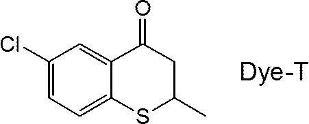
・TPP:亜リン酸トリフェニル
・DDT:1-ドデカンチオール
・UC-203:液状ゴム(イソプレン重合物の無水マレイン酸付加物と2-ヒドロキシエチルメタクリレートとのエステル化物、1分子当りのメタクリロイル基数:3、重量平均分子量:35000、クラレ社製)
・UC-102:液状ゴム(イソプレン重合物の無水マレイン酸付加物と2-ヒドロキシエチルメタクリレートとのエステル化物、1分子当たりのメタクリロイル基数:2、重量平均分子量:19000、クラレ社製)
・P-135:CLEARON P-135(水添テルペン樹脂、ヤスハラケミカル社製)
・Polyoil 110:液状ポリブタジエン(日本ゼオン社製)
・EHMA:2-エチルヘキシルメタクリレート(SP値:8.1)
・CHMA:シクロヘキシルメタクリレート(SP値:8.3)
・IBXA:イソボルニルアクリレート(SP値:8.33)
・HEMA:2-ヒドロキシエチルメタクリレート(SP値:9.39)
・MMA:メチルメタクリレート(SP値:8.2)
・FA-512M:ジシクロペンテニルオキシエチルメタクリレート、日立化成社製
・FA-512AS:ジシクロペンテニルオキシエチルアクリレート、日立化成社製
・EHA:2-エチルヘキシルアクリレート(SP値:7.8)
・IBX:イソボルニルメタクリレート(SP値:8.3)
・StMA:ステアリルメタクリレート
・TPO:Lucirin TPO(2,4,6-トリメチルベンゾイル-ジフェニルホスフィンオキサイド、BASF社製)(0.1質量%アセトニトリル溶液の400nmにおける吸光度:1.0)
・TPO-L:Lucirin TPO-L(2,4,6-トリメチルベンゾイル-フェニルエトキシホスフィンオキサイド、BASF社製)(0.1質量%アセトニトリル溶液の400nmにおける吸光度:0.4)
・IRG819:Irgacure819(ビス(2,4,6-トリメチルベンゾイル)-フェニルホスフィンオキサイド、BASF社製)(0.1質量%アセトニトリル溶液の430nmにおける吸光度:0.25)
・IRG369:Irgacure369(2-ベンジル-2-ジメチルアミノ-1-(4-モルフォリノフェニル)-ブタノン-1、BASF社製)
・IRG184:Irgacure184(1-ヒドロキシ-シクロヘキシル-フェニル-ケトン、BASF社製)
・Dye-T:チオクロマノン化合物(下記化合物)
・TPP:亜リン酸トリフェニル
・DDT:1-ドデカンチオール
・UC-203:液状ゴム(イソプレン重合物の無水マレイン酸付加物と2-ヒドロキシエチルメタクリレートとのエステル化物、1分子当りのメタクリロイル基数:3、重量平均分子量:35000、クラレ社製)
・UC-102:液状ゴム(イソプレン重合物の無水マレイン酸付加物と2-ヒドロキシエチルメタクリレートとのエステル化物、1分子当たりのメタクリロイル基数:2、重量平均分子量:19000、クラレ社製)
・P-135:CLEARON P-135(水添テルペン樹脂、ヤスハラケミカル社製)
・Polyoil 110:液状ポリブタジエン(日本ゼオン社製)
表1から分かるように、モノアシルホスフィンオキサイド(A1)に加えてビスアシルホスフィンオキサイド(A2)を併用し、かつ、特定のラジカル重合性モノマー(B)を使用するとともに、O/C比を特定にした実施例1~25の粘着剤組成物は、いずれも粘着シートとしたときに優れた密着性を示した。また、粘着シートとして静電容量式タッチパネルに用いたときに低温から高温までの幅広い温度環境下にて誤動作の発生が抑制されていた。
実施例1~3の対比から、ビスアシルホスフィンオキサイド(A2)の含有量(a2)とモノアシルホスフィンオキサイド(A1)の含有量(a1)との質量比(a2/a1)が0.30以上である実施例2および3の方がより優れた密着性および段差追従性を示した。なかでも、質量比(a2/a1)が0.40以上である実施例3はさらに優れた密着性を示した。
実施例3~5の対比から、ラジカル重合性モノマー(B)の含有量(b)と、モノアシルホスフィンオキサイド(A1)およびビスアシルホスフィンオキサイド(A2)の合計の含有量(a)との質量比(b/a)が4.0以上である実施例3および4の方がより優れた密着性および段差追従性を示した。また、実施例3~4および17~18の対比から、質量比(b/a)が6.0以上である実施例3および17はさらに優れた段差追従性を示すとともに、誤動作の発生がより抑制されていた。
実施例1~3の対比から、ビスアシルホスフィンオキサイド(A2)の含有量(a2)とモノアシルホスフィンオキサイド(A1)の含有量(a1)との質量比(a2/a1)が0.30以上である実施例2および3の方がより優れた密着性および段差追従性を示した。なかでも、質量比(a2/a1)が0.40以上である実施例3はさらに優れた密着性を示した。
実施例3~5の対比から、ラジカル重合性モノマー(B)の含有量(b)と、モノアシルホスフィンオキサイド(A1)およびビスアシルホスフィンオキサイド(A2)の合計の含有量(a)との質量比(b/a)が4.0以上である実施例3および4の方がより優れた密着性および段差追従性を示した。また、実施例3~4および17~18の対比から、質量比(b/a)が6.0以上である実施例3および17はさらに優れた段差追従性を示すとともに、誤動作の発生がより抑制されていた。
一方、モノアシルホスフィンオキサイド(A1)とビスアシルホスフィンオキサイド(A2)を併用せずに、モノアシルホスフィンオキサイド(A1)のみを使用した比較例1~5および7はいずれも密着性が不十分であった。また、誤動作発生率が高い場合があった。
また、ビスアシルホスフィンオキサイド(A2)のみを使用した比較例8は粘着シートを形成することができるような均質な組成物が得られなかった。
また、モノアシルホスフィンオキサイド(A1)とビスアシルホスフィンオキサイド(A2)を併用するが、特定のラジカル重合性モノマー(B)を使用しない比較例11~13および15は密着性が不十分であり、また、誤動作発生率が高かった。
また、モノアシルホスフィンオキサイド(A1)とビスアシルホスフィンオキサイド(A2)を併用し、かつ、特定のラジカル重合性モノマー(B)を使用するが、質量比(b/a)が3.0未満である比較例14は粘着シートを形成することができるような均質な組成物が得られなかった。
また、モノアシルホスフィンオキサイド(A1)とビスアシルホスフィンオキサイド(A2)を併用し、かつ、特定のラジカル重合性モノマー(B)を使用するが、組成物全量に対するモノアシルホスフィンオキサイド(A1)の含有量が1.5質量%未満である比較例6は密着性が不十分であり、また、誤動作発生率が高かった。
また、ビスアシルホスフィンオキサイド(A2)のみを使用した比較例8は粘着シートを形成することができるような均質な組成物が得られなかった。
また、モノアシルホスフィンオキサイド(A1)とビスアシルホスフィンオキサイド(A2)を併用するが、特定のラジカル重合性モノマー(B)を使用しない比較例11~13および15は密着性が不十分であり、また、誤動作発生率が高かった。
また、モノアシルホスフィンオキサイド(A1)とビスアシルホスフィンオキサイド(A2)を併用し、かつ、特定のラジカル重合性モノマー(B)を使用するが、質量比(b/a)が3.0未満である比較例14は粘着シートを形成することができるような均質な組成物が得られなかった。
また、モノアシルホスフィンオキサイド(A1)とビスアシルホスフィンオキサイド(A2)を併用し、かつ、特定のラジカル重合性モノマー(B)を使用するが、組成物全量に対するモノアシルホスフィンオキサイド(A1)の含有量が1.5質量%未満である比較例6は密着性が不十分であり、また、誤動作発生率が高かった。
12 粘着シート
18、180、180a、280、380 静電容量式タッチパネルセンサー
20 保護基板
22 基板
24、24a 第1検出電極
26、26a 第1引き出し配線
28、28a 第2検出電極
30 第2引き出し配線
32 フレキシブルプリント配線板
34 導電性細線
36 格子
38 第1基板
40 粘着シート
42 第2基板
50 表示装置
60 保護基板一体型静電容量式タッチパネルセンサー
100、200 タッチパネル用積層体
300、400、500 静電容量式タッチパネル
18、180、180a、280、380 静電容量式タッチパネルセンサー
20 保護基板
22 基板
24、24a 第1検出電極
26、26a 第1引き出し配線
28、28a 第2検出電極
30 第2引き出し配線
32 フレキシブルプリント配線板
34 導電性細線
36 格子
38 第1基板
40 粘着シート
42 第2基板
50 表示装置
60 保護基板一体型静電容量式タッチパネルセンサー
100、200 タッチパネル用積層体
300、400、500 静電容量式タッチパネル
Claims (10)
- モノアシルホスフィンオキサイドA1と、ビスアシルホスフィンオキサイドA2と、溶解度パラメータが8.0~10.0であるラジカル重合性モノマーBとを含有する粘着剤組成物であって、
前記ラジカル重合性モノマーBが、分岐状アルキル基および脂環式炭化水素基からなる群より選択される少なくとも1種の基を有し、
前記粘着剤組成物の全量に対する前記モノアシルホスフィンオキサイドA1の含有量が、1.5質量%以上であり、
前記ラジカル重合性モノマーBの含有量bと、前記モノアシルホスフィンオキサイドA1および前記ビスアシルホスフィンオキサイドA2の合計の含有量aとの質量比b/aが、3.0~30.0であり、
前記粘着剤組成物に含まれる酸素原子のモル数と炭素原子のモル数との比が、0.1以下である、粘着剤組成物。
ただし、前記脂環式炭化水素基は、不飽和炭化水素基を有する脂環式炭化水素基以外の脂環式炭化水素基である。前記酸素原子のモル数と炭素原子のモル数との比は、前記炭素原子のモル数に対する前記酸素原子のモル数の比である。 - さらに、アミノケトン系光重合開始剤およびヒドロキシケトン系光重合開始剤からなる群より選択される少なくとも1種の光重合開始剤を含有する、請求項1に記載の粘着剤組成物。
- さらに、下記一般式(I)で表される増感色素を含有する、請求項1または2に記載の粘着剤組成物。

一般式(I)中、R11~R18は、それぞれ独立に、水素原子、アルキル基、ハロゲン原子、ヒドロキシ基、シアノ基、ニトロ基、アミノ基、アルキルチオ基、アルキルアミノ基、アルコキシ基、アルコキシカルボニル基、アシルオキシ基、アシル基、カルボキシル基またはスルホ基を表す。R15またはR16と、R17またはR18とは、互いに結合して5~6員の脂肪族環、芳香族環、または複素環を形成していてもよい。 - さらに、亜リン酸エステル、アミンおよびチオールからなる群より選択される少なくとも1種の重合阻害抑制剤を含有する、請求項1~3のいずれか1項に記載の粘着剤組成物。
- 請求項1~4のいずれか1項に記載の粘着剤組成物から得られる粘着シート。
- 厚みが50μm以上である、請求項5に記載の粘着シート。
- タッチパネル用粘着シートである、請求項5または6に記載の粘着シート。
- 請求項7に記載の粘着シートと、静電容量式タッチパネルセンサーとを備える、タッチパネル用積層体。
- さらに、保護基板を備え、
前記保護基板と、前記粘着シートと、前記静電容量式タッチパネルセンサーとをこの順に備える、請求項8に記載のタッチパネル用積層体。 - 静電容量式タッチパネルセンサーと、請求項7に記載の粘着シートと、表示装置とをこの順に備える、静電容量式タッチパネル。
Applications Claiming Priority (4)
| Application Number | Priority Date | Filing Date | Title |
|---|---|---|---|
| JP2013200324 | 2013-09-26 | ||
| JP2013-200324 | 2013-09-26 | ||
| JP2014-038297 | 2014-02-28 | ||
| JP2014038297A JP5961201B2 (ja) | 2013-09-26 | 2014-02-28 | 粘着剤組成物、粘着シート、タッチパネル用積層体および静電容量式タッチパネル |
Publications (1)
| Publication Number | Publication Date |
|---|---|
| WO2015045758A1 true WO2015045758A1 (ja) | 2015-04-02 |
Family
ID=52742905
Family Applications (1)
| Application Number | Title | Priority Date | Filing Date |
|---|---|---|---|
| PCT/JP2014/073079 Ceased WO2015045758A1 (ja) | 2013-09-26 | 2014-09-02 | 粘着剤組成物、粘着シート、タッチパネル用積層体および静電容量式タッチパネル |
Country Status (2)
| Country | Link |
|---|---|
| JP (1) | JP5961201B2 (ja) |
| WO (1) | WO2015045758A1 (ja) |
Cited By (2)
| Publication number | Priority date | Publication date | Assignee | Title |
|---|---|---|---|---|
| WO2017014269A1 (ja) * | 2015-07-23 | 2017-01-26 | 三菱樹脂株式会社 | 導電部材用粘着剤組成物 |
| CN113631369A (zh) * | 2019-03-28 | 2021-11-09 | 富士胶片株式会社 | 层叠体、附被镀覆层基板的制造方法、导电性薄膜的制造方法 |
Families Citing this family (2)
| Publication number | Priority date | Publication date | Assignee | Title |
|---|---|---|---|---|
| JP2017120363A (ja) * | 2015-12-25 | 2017-07-06 | 日東電工株式会社 | 粘着剤層付き偏光フィルム、及び画像表示装置 |
| US12435206B2 (en) | 2021-03-19 | 2025-10-07 | Samsung Display Co., Ltd. | Resin composition, adhesive member, and display device including the same |
Citations (4)
| Publication number | Priority date | Publication date | Assignee | Title |
|---|---|---|---|---|
| JPH10102007A (ja) * | 1996-10-02 | 1998-04-21 | Showa Denko Kk | 光ディスク基板貼り合わせ用接着剤及び光ディスクの製造方法 |
| JP2006307151A (ja) * | 2005-03-31 | 2006-11-09 | Emulsion Technology Co Ltd | 紫外線硬化型紫外線遮蔽性樹脂組成物 |
| JP2011213919A (ja) * | 2010-03-31 | 2011-10-27 | Furukawa Electric Co Ltd:The | 放射線硬化性半導体ウエハ表面保護用粘着テープ |
| WO2014142263A1 (ja) * | 2013-03-13 | 2014-09-18 | 富士フイルム株式会社 | 静電容量式タッチパネル |
Family Cites Families (1)
| Publication number | Priority date | Publication date | Assignee | Title |
|---|---|---|---|---|
| JP4756127B2 (ja) * | 2003-10-30 | 2011-08-24 | 綜研化学株式会社 | (メタ)アクリル系重合体の製造方法 |
-
2014
- 2014-02-28 JP JP2014038297A patent/JP5961201B2/ja not_active Expired - Fee Related
- 2014-09-02 WO PCT/JP2014/073079 patent/WO2015045758A1/ja not_active Ceased
Patent Citations (4)
| Publication number | Priority date | Publication date | Assignee | Title |
|---|---|---|---|---|
| JPH10102007A (ja) * | 1996-10-02 | 1998-04-21 | Showa Denko Kk | 光ディスク基板貼り合わせ用接着剤及び光ディスクの製造方法 |
| JP2006307151A (ja) * | 2005-03-31 | 2006-11-09 | Emulsion Technology Co Ltd | 紫外線硬化型紫外線遮蔽性樹脂組成物 |
| JP2011213919A (ja) * | 2010-03-31 | 2011-10-27 | Furukawa Electric Co Ltd:The | 放射線硬化性半導体ウエハ表面保護用粘着テープ |
| WO2014142263A1 (ja) * | 2013-03-13 | 2014-09-18 | 富士フイルム株式会社 | 静電容量式タッチパネル |
Cited By (3)
| Publication number | Priority date | Publication date | Assignee | Title |
|---|---|---|---|---|
| WO2017014269A1 (ja) * | 2015-07-23 | 2017-01-26 | 三菱樹脂株式会社 | 導電部材用粘着剤組成物 |
| CN113631369A (zh) * | 2019-03-28 | 2021-11-09 | 富士胶片株式会社 | 层叠体、附被镀覆层基板的制造方法、导电性薄膜的制造方法 |
| CN113631369B (zh) * | 2019-03-28 | 2023-05-02 | 富士胶片株式会社 | 层叠体、附被镀覆层基板的制造方法、导电性薄膜的制造方法 |
Also Published As
| Publication number | Publication date |
|---|---|
| JP5961201B2 (ja) | 2016-08-02 |
| JP2015086353A (ja) | 2015-05-07 |
Similar Documents
| Publication | Publication Date | Title |
|---|---|---|
| TWI590136B (zh) | 靜電電容式觸碰面板及其製造方法以及輸入裝置 | |
| JP6092363B2 (ja) | 粘着フィルム、タッチパネル用積層体 | |
| JP5689931B2 (ja) | 粘着シート、タッチパネル用積層体、静電容量式タッチパネル | |
| JP6088467B2 (ja) | タッチパネル用粘着シート、タッチパネル用積層体、静電容量式タッチパネル | |
| JP6026447B2 (ja) | タッチパネル用積層体、フラットパネルディスプレイ | |
| JP6148217B2 (ja) | タッチパネル用粘着フィルム、タッチパネル用積層体、粘着層の剥離方法、タッチパネルの使用方法、タッチパネルシステム | |
| JP5926445B2 (ja) | 静電容量式タッチパネル | |
| WO2015129308A1 (ja) | タッチパネル用積層体、および、粘着シート | |
| JP6042853B2 (ja) | タッチパネル用粘着フィルム、タッチパネル用積層体、粘着層の剥離方法、タッチパネルの使用方法、タッチパネルシステム | |
| JPWO2015146347A1 (ja) | 導電膜積層体、およびこれを用いるタッチパネル | |
| WO2015053230A1 (ja) | タッチパネル用積層体 | |
| JP5961201B2 (ja) | 粘着剤組成物、粘着シート、タッチパネル用積層体および静電容量式タッチパネル | |
| WO2015076087A1 (ja) | 静電容量式タッチパネル | |
| JP5926444B2 (ja) | 静電容量式タッチパネル | |
| WO2015141323A1 (ja) | 粘着シートの製造方法、粘着シート、タッチパネル用積層体および静電容量式タッチパネル | |
| JP2016138184A (ja) | 両面粘着シート、剥離フィルム付き両面粘着シート、および、静電容量式タッチパネル | |
| WO2015133223A1 (ja) | タッチパネル用粘着フィルムおよびタッチパネル用積層体 | |
| JP2016023201A (ja) | 光硬化性組成物、粘着シート、タッチパネル用積層体および静電容量式タッチパネル | |
| WO2016027580A1 (ja) | 活性エネルギー線硬化性樹脂組成物、光学用部材、粘着シート、タッチパネル用積層体および静電容量式タッチパネル | |
| JP6126526B2 (ja) | タッチパネル用粘着フィルム、タッチパネル用積層体 | |
| JP2015086277A (ja) | 粘着シートの製造方法、粘着シート、タッチパネル用積層体および静電容量式タッチパネル |
Legal Events
| Date | Code | Title | Description |
|---|---|---|---|
| 121 | Ep: the epo has been informed by wipo that ep was designated in this application |
Ref document number: 14847040 Country of ref document: EP Kind code of ref document: A1 |
|
| NENP | Non-entry into the national phase |
Ref country code: DE |
|
| 122 | Ep: pct application non-entry in european phase |
Ref document number: 14847040 Country of ref document: EP Kind code of ref document: A1 |