WO2015037331A1 - 表示装置およびその駆動方法 - Google Patents
表示装置およびその駆動方法 Download PDFInfo
- Publication number
- WO2015037331A1 WO2015037331A1 PCT/JP2014/069285 JP2014069285W WO2015037331A1 WO 2015037331 A1 WO2015037331 A1 WO 2015037331A1 JP 2014069285 W JP2014069285 W JP 2014069285W WO 2015037331 A1 WO2015037331 A1 WO 2015037331A1
- Authority
- WO
- WIPO (PCT)
- Prior art keywords
- period
- circuit
- measurement
- voltage
- drive
- Prior art date
- Legal status (The legal status is an assumption and is not a legal conclusion. Google has not performed a legal analysis and makes no representation as to the accuracy of the status listed.)
- Ceased
Links
Images








Classifications
-
- G—PHYSICS
- G09—EDUCATION; CRYPTOGRAPHY; DISPLAY; ADVERTISING; SEALS
- G09G—ARRANGEMENTS OR CIRCUITS FOR CONTROL OF INDICATING DEVICES USING STATIC MEANS TO PRESENT VARIABLE INFORMATION
- G09G3/00—Control arrangements or circuits, of interest only in connection with visual indicators other than cathode-ray tubes
- G09G3/20—Control arrangements or circuits, of interest only in connection with visual indicators other than cathode-ray tubes for presentation of an assembly of a number of characters, e.g. a page, by composing the assembly by combination of individual elements arranged in a matrix no fixed position being assigned to or needed to be assigned to the individual characters or partial characters
- G09G3/22—Control arrangements or circuits, of interest only in connection with visual indicators other than cathode-ray tubes for presentation of an assembly of a number of characters, e.g. a page, by composing the assembly by combination of individual elements arranged in a matrix no fixed position being assigned to or needed to be assigned to the individual characters or partial characters using controlled light sources
- G09G3/30—Control arrangements or circuits, of interest only in connection with visual indicators other than cathode-ray tubes for presentation of an assembly of a number of characters, e.g. a page, by composing the assembly by combination of individual elements arranged in a matrix no fixed position being assigned to or needed to be assigned to the individual characters or partial characters using controlled light sources using electroluminescent panels
- G09G3/32—Control arrangements or circuits, of interest only in connection with visual indicators other than cathode-ray tubes for presentation of an assembly of a number of characters, e.g. a page, by composing the assembly by combination of individual elements arranged in a matrix no fixed position being assigned to or needed to be assigned to the individual characters or partial characters using controlled light sources using electroluminescent panels semiconductive, e.g. using light-emitting diodes [LED]
- G09G3/3208—Control arrangements or circuits, of interest only in connection with visual indicators other than cathode-ray tubes for presentation of an assembly of a number of characters, e.g. a page, by composing the assembly by combination of individual elements arranged in a matrix no fixed position being assigned to or needed to be assigned to the individual characters or partial characters using controlled light sources using electroluminescent panels semiconductive, e.g. using light-emitting diodes [LED] organic, e.g. using organic light-emitting diodes [OLED]
- G09G3/3225—Control arrangements or circuits, of interest only in connection with visual indicators other than cathode-ray tubes for presentation of an assembly of a number of characters, e.g. a page, by composing the assembly by combination of individual elements arranged in a matrix no fixed position being assigned to or needed to be assigned to the individual characters or partial characters using controlled light sources using electroluminescent panels semiconductive, e.g. using light-emitting diodes [LED] organic, e.g. using organic light-emitting diodes [OLED] using an active matrix
- G09G3/3233—Control arrangements or circuits, of interest only in connection with visual indicators other than cathode-ray tubes for presentation of an assembly of a number of characters, e.g. a page, by composing the assembly by combination of individual elements arranged in a matrix no fixed position being assigned to or needed to be assigned to the individual characters or partial characters using controlled light sources using electroluminescent panels semiconductive, e.g. using light-emitting diodes [LED] organic, e.g. using organic light-emitting diodes [OLED] using an active matrix with pixel circuitry controlling the current through the light-emitting element
-
- G—PHYSICS
- G09—EDUCATION; CRYPTOGRAPHY; DISPLAY; ADVERTISING; SEALS
- G09G—ARRANGEMENTS OR CIRCUITS FOR CONTROL OF INDICATING DEVICES USING STATIC MEANS TO PRESENT VARIABLE INFORMATION
- G09G3/00—Control arrangements or circuits, of interest only in connection with visual indicators other than cathode-ray tubes
- G09G3/20—Control arrangements or circuits, of interest only in connection with visual indicators other than cathode-ray tubes for presentation of an assembly of a number of characters, e.g. a page, by composing the assembly by combination of individual elements arranged in a matrix no fixed position being assigned to or needed to be assigned to the individual characters or partial characters
- G09G3/22—Control arrangements or circuits, of interest only in connection with visual indicators other than cathode-ray tubes for presentation of an assembly of a number of characters, e.g. a page, by composing the assembly by combination of individual elements arranged in a matrix no fixed position being assigned to or needed to be assigned to the individual characters or partial characters using controlled light sources
- G09G3/30—Control arrangements or circuits, of interest only in connection with visual indicators other than cathode-ray tubes for presentation of an assembly of a number of characters, e.g. a page, by composing the assembly by combination of individual elements arranged in a matrix no fixed position being assigned to or needed to be assigned to the individual characters or partial characters using controlled light sources using electroluminescent panels
-
- G—PHYSICS
- G09—EDUCATION; CRYPTOGRAPHY; DISPLAY; ADVERTISING; SEALS
- G09G—ARRANGEMENTS OR CIRCUITS FOR CONTROL OF INDICATING DEVICES USING STATIC MEANS TO PRESENT VARIABLE INFORMATION
- G09G3/00—Control arrangements or circuits, of interest only in connection with visual indicators other than cathode-ray tubes
- G09G3/20—Control arrangements or circuits, of interest only in connection with visual indicators other than cathode-ray tubes for presentation of an assembly of a number of characters, e.g. a page, by composing the assembly by combination of individual elements arranged in a matrix no fixed position being assigned to or needed to be assigned to the individual characters or partial characters
- G09G3/22—Control arrangements or circuits, of interest only in connection with visual indicators other than cathode-ray tubes for presentation of an assembly of a number of characters, e.g. a page, by composing the assembly by combination of individual elements arranged in a matrix no fixed position being assigned to or needed to be assigned to the individual characters or partial characters using controlled light sources
- G09G3/30—Control arrangements or circuits, of interest only in connection with visual indicators other than cathode-ray tubes for presentation of an assembly of a number of characters, e.g. a page, by composing the assembly by combination of individual elements arranged in a matrix no fixed position being assigned to or needed to be assigned to the individual characters or partial characters using controlled light sources using electroluminescent panels
- G09G3/32—Control arrangements or circuits, of interest only in connection with visual indicators other than cathode-ray tubes for presentation of an assembly of a number of characters, e.g. a page, by composing the assembly by combination of individual elements arranged in a matrix no fixed position being assigned to or needed to be assigned to the individual characters or partial characters using controlled light sources using electroluminescent panels semiconductive, e.g. using light-emitting diodes [LED]
- G09G3/3208—Control arrangements or circuits, of interest only in connection with visual indicators other than cathode-ray tubes for presentation of an assembly of a number of characters, e.g. a page, by composing the assembly by combination of individual elements arranged in a matrix no fixed position being assigned to or needed to be assigned to the individual characters or partial characters using controlled light sources using electroluminescent panels semiconductive, e.g. using light-emitting diodes [LED] organic, e.g. using organic light-emitting diodes [OLED]
- G09G3/3266—Details of drivers for scan electrodes
-
- G—PHYSICS
- G09—EDUCATION; CRYPTOGRAPHY; DISPLAY; ADVERTISING; SEALS
- G09G—ARRANGEMENTS OR CIRCUITS FOR CONTROL OF INDICATING DEVICES USING STATIC MEANS TO PRESENT VARIABLE INFORMATION
- G09G3/00—Control arrangements or circuits, of interest only in connection with visual indicators other than cathode-ray tubes
- G09G3/20—Control arrangements or circuits, of interest only in connection with visual indicators other than cathode-ray tubes for presentation of an assembly of a number of characters, e.g. a page, by composing the assembly by combination of individual elements arranged in a matrix no fixed position being assigned to or needed to be assigned to the individual characters or partial characters
- G09G3/22—Control arrangements or circuits, of interest only in connection with visual indicators other than cathode-ray tubes for presentation of an assembly of a number of characters, e.g. a page, by composing the assembly by combination of individual elements arranged in a matrix no fixed position being assigned to or needed to be assigned to the individual characters or partial characters using controlled light sources
- G09G3/30—Control arrangements or circuits, of interest only in connection with visual indicators other than cathode-ray tubes for presentation of an assembly of a number of characters, e.g. a page, by composing the assembly by combination of individual elements arranged in a matrix no fixed position being assigned to or needed to be assigned to the individual characters or partial characters using controlled light sources using electroluminescent panels
- G09G3/32—Control arrangements or circuits, of interest only in connection with visual indicators other than cathode-ray tubes for presentation of an assembly of a number of characters, e.g. a page, by composing the assembly by combination of individual elements arranged in a matrix no fixed position being assigned to or needed to be assigned to the individual characters or partial characters using controlled light sources using electroluminescent panels semiconductive, e.g. using light-emitting diodes [LED]
- G09G3/3208—Control arrangements or circuits, of interest only in connection with visual indicators other than cathode-ray tubes for presentation of an assembly of a number of characters, e.g. a page, by composing the assembly by combination of individual elements arranged in a matrix no fixed position being assigned to or needed to be assigned to the individual characters or partial characters using controlled light sources using electroluminescent panels semiconductive, e.g. using light-emitting diodes [LED] organic, e.g. using organic light-emitting diodes [OLED]
- G09G3/3275—Details of drivers for data electrodes
- G09G3/3291—Details of drivers for data electrodes in which the data driver supplies a variable data voltage for setting the current through, or the voltage across, the light-emitting elements
-
- G—PHYSICS
- G09—EDUCATION; CRYPTOGRAPHY; DISPLAY; ADVERTISING; SEALS
- G09G—ARRANGEMENTS OR CIRCUITS FOR CONTROL OF INDICATING DEVICES USING STATIC MEANS TO PRESENT VARIABLE INFORMATION
- G09G2300/00—Aspects of the constitution of display devices
- G09G2300/08—Active matrix structure, i.e. with use of active elements, inclusive of non-linear two terminal elements, in the pixels together with light emitting or modulating elements
- G09G2300/0809—Several active elements per pixel in active matrix panels
-
- G—PHYSICS
- G09—EDUCATION; CRYPTOGRAPHY; DISPLAY; ADVERTISING; SEALS
- G09G—ARRANGEMENTS OR CIRCUITS FOR CONTROL OF INDICATING DEVICES USING STATIC MEANS TO PRESENT VARIABLE INFORMATION
- G09G2300/00—Aspects of the constitution of display devices
- G09G2300/08—Active matrix structure, i.e. with use of active elements, inclusive of non-linear two terminal elements, in the pixels together with light emitting or modulating elements
- G09G2300/0809—Several active elements per pixel in active matrix panels
- G09G2300/0842—Several active elements per pixel in active matrix panels forming a memory circuit, e.g. a dynamic memory with one capacitor
-
- G—PHYSICS
- G09—EDUCATION; CRYPTOGRAPHY; DISPLAY; ADVERTISING; SEALS
- G09G—ARRANGEMENTS OR CIRCUITS FOR CONTROL OF INDICATING DEVICES USING STATIC MEANS TO PRESENT VARIABLE INFORMATION
- G09G2310/00—Command of the display device
- G09G2310/02—Addressing, scanning or driving the display screen or processing steps related thereto
- G09G2310/0264—Details of driving circuits
- G09G2310/0291—Details of output amplifiers or buffers arranged for use in a driving circuit
-
- G—PHYSICS
- G09—EDUCATION; CRYPTOGRAPHY; DISPLAY; ADVERTISING; SEALS
- G09G—ARRANGEMENTS OR CIRCUITS FOR CONTROL OF INDICATING DEVICES USING STATIC MEANS TO PRESENT VARIABLE INFORMATION
- G09G2310/00—Command of the display device
- G09G2310/08—Details of timing specific for flat panels, other than clock recovery
-
- G—PHYSICS
- G09—EDUCATION; CRYPTOGRAPHY; DISPLAY; ADVERTISING; SEALS
- G09G—ARRANGEMENTS OR CIRCUITS FOR CONTROL OF INDICATING DEVICES USING STATIC MEANS TO PRESENT VARIABLE INFORMATION
- G09G2320/00—Control of display operating conditions
- G09G2320/02—Improving the quality of display appearance
- G09G2320/0233—Improving the luminance or brightness uniformity across the screen
-
- G—PHYSICS
- G09—EDUCATION; CRYPTOGRAPHY; DISPLAY; ADVERTISING; SEALS
- G09G—ARRANGEMENTS OR CIRCUITS FOR CONTROL OF INDICATING DEVICES USING STATIC MEANS TO PRESENT VARIABLE INFORMATION
- G09G2320/00—Control of display operating conditions
- G09G2320/02—Improving the quality of display appearance
- G09G2320/0271—Adjustment of the gradation levels within the range of the gradation scale, e.g. by redistribution or clipping
- G09G2320/0276—Adjustment of the gradation levels within the range of the gradation scale, e.g. by redistribution or clipping for the purpose of adaptation to the characteristics of a display device, i.e. gamma correction
-
- G—PHYSICS
- G09—EDUCATION; CRYPTOGRAPHY; DISPLAY; ADVERTISING; SEALS
- G09G—ARRANGEMENTS OR CIRCUITS FOR CONTROL OF INDICATING DEVICES USING STATIC MEANS TO PRESENT VARIABLE INFORMATION
- G09G2320/00—Control of display operating conditions
- G09G2320/02—Improving the quality of display appearance
- G09G2320/0285—Improving the quality of display appearance using tables for spatial correction of display data
-
- G—PHYSICS
- G09—EDUCATION; CRYPTOGRAPHY; DISPLAY; ADVERTISING; SEALS
- G09G—ARRANGEMENTS OR CIRCUITS FOR CONTROL OF INDICATING DEVICES USING STATIC MEANS TO PRESENT VARIABLE INFORMATION
- G09G2320/00—Control of display operating conditions
- G09G2320/02—Improving the quality of display appearance
- G09G2320/029—Improving the quality of display appearance by monitoring one or more pixels in the display panel, e.g. by monitoring a fixed reference pixel
- G09G2320/0295—Improving the quality of display appearance by monitoring one or more pixels in the display panel, e.g. by monitoring a fixed reference pixel by monitoring each display pixel
-
- G—PHYSICS
- G09—EDUCATION; CRYPTOGRAPHY; DISPLAY; ADVERTISING; SEALS
- G09G—ARRANGEMENTS OR CIRCUITS FOR CONTROL OF INDICATING DEVICES USING STATIC MEANS TO PRESENT VARIABLE INFORMATION
- G09G2330/00—Aspects of power supply; Aspects of display protection and defect management
- G09G2330/02—Details of power systems and of start or stop of display operation
- G09G2330/021—Power management, e.g. power saving
Definitions
- the present invention relates to a display device, and more particularly, to a display device including a current-driven light emitting element such as an organic EL element and a driving method thereof.
- organic EL (Electro Luminescence) display devices have attracted attention as display devices that are thin, lightweight, and capable of high-speed response.
- the organic EL display device includes a plurality of pixel circuits arranged two-dimensionally.
- the pixel circuit of the organic EL display device includes an organic EL element and a driving transistor.
- the drive transistor is provided in series with the organic EL element, and controls the amount of current flowing through the organic EL element (hereinafter referred to as drive current).
- the organic EL element emits light with a luminance corresponding to the amount of drive current.
- the characteristics (threshold voltage and mobility) of the drive transistor vary.
- variations in the characteristics of the drive transistors variations in the amount of drive current occur, resulting in uneven brightness on the display screen.
- Patent Document 1 discloses an organic EL display in which a drive current is read out via a power supply line, a correction gain and a correction offset are updated based on the measured amount of drive current, and a video signal is corrected using these.
- An apparatus is described.
- the drive current is read out via a data line, the threshold voltage of the drive transistor is updated based on the comparison result between the measured drive current amount and the target amount, and the video signal is corrected using this.
- An organic EL display device is described.
- Pause driving is a driving method in which when the same image is continuously displayed, the frame period is classified into a driving period and a pausing period, the driving circuit is operated during the driving period, and the operation of the driving circuit is stopped during the pausing period.
- the pause drive can be applied when the off-leak characteristics of the transistors in the pixel circuit are good (the off-leak current is small).
- Patent Document 3 A display device that performs pause driving is described in Patent Document 3, for example.
- a voltage corresponding to a video signal (hereinafter referred to as a data voltage) is written to pixel circuits in all rows within one frame period, and output from the pixel circuits for one row.
- a display device that measures the measured drive current is referred to as a pixel circuit to be measured.
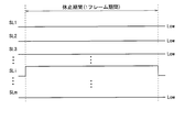
- FIG. 18 is a timing chart of the display device according to the comparative example.
- FIG. 18 shows changes in the voltages of the scanning lines SL1 to SLm when the pixel circuit in the i-th row is the measurement target.
- the voltages of the scanning lines SL1 to SLm are controlled to the high level in order of one line period (each time Ts1).
- the voltage of the scanning line SLi is controlled to the high level only for the time Ts2 (> Ts1) in order to perform the writing of the data voltage and the measurement of the driving current.
- the time Ts2 is, for example, about several times the time Ts1.
- the selection period of the scanning line SLi corresponding to the pixel circuit to be measured is longer than the selection period of the other scanning lines.
- scanning lines whose selection period is longer than other scanning lines are switched every frame period.
- a scanning line driving circuit of a display device is generally configured by connecting flip-flops in multiple stages, supplying a clock signal to the clock terminal of each stage flip-flop, and supplying a start pulse to the input terminal of the first stage flip-flop.
- the scanning line driving circuit of the display device according to the comparative example needs to control the scanning line voltage as shown in FIG. For this reason, in the display device according to the comparative example, the configuration of the scanning line driving circuit is more complicated than in a general display device.
- the drive current is a minute current of the order of ⁇ A or less, it is necessary to lengthen the measurement time in order to accurately measure the drive current.
- the data voltage is written to the pixel circuits in all rows within one frame period, so that it is not possible to secure a sufficient time for measuring the drive current.
- the display device according to the comparative example has a problem in that variations in characteristics of the drive transistor cannot be sufficiently compensated, and luminance unevenness in the display screen cannot be sufficiently suppressed.
- the display device according to the comparative example also has a problem that power consumption at the peak time is large because data voltage writing and driving current measurement are performed in the same frame period.
- an object of the present invention is to provide a low power consumption display device that has a scanning line driving circuit with a simple configuration and can effectively suppress uneven luminance, and a driving method thereof.
- a first aspect of the present invention is a display device including a current-driven light emitting element, A plurality of pixel circuits arranged corresponding to the intersections of the plurality of scanning lines and the plurality of data lines; A driving circuit for writing a voltage to the pixel circuit by driving the scanning line and the data line; A measurement circuit for measuring the drive current output from the pixel circuit to the data line; A correction circuit for correcting the video signal based on the drive current measured by the measurement circuit;
- the pixel circuit includes: A light emitting element; A driving transistor that is provided in series with the light emitting element and outputs a driving current in an amount corresponding to a voltage between a control terminal and the conduction terminal on the light emitting element side; An input / output transistor provided between a conduction terminal on the light emitting element side of the driving transistor and the data line, and having a control terminal connected to the scanning line;
- the drive circuit classifies the frame period into a drive period and a pause period, and in the drive period, a selection voltage is sequential
- the drive circuit applies a voltage corresponding to the corrected video signal to the data line during a scanning line selection period corresponding to a pixel circuit that is not a measurement target within the drive period, and the measurement target pixel circuit within the drive period A measuring voltage is applied to the data line in a scanning line selection period corresponding to the above.
- the drive circuit classifies the four frame periods in order into a first drive period, a first idle period, a second drive period, and a second idle period, and corresponds to the pixel circuit to be measured in the first drive period
- the first measurement voltage is applied to the data line
- the second measurement voltage is applied to the data line.
- the measurement circuit measures the drive current output from the pixel circuit to be measured as the first drive current in the first pause period, and performs the second drive on the drive current output from the pixel circuit to be measured in the second pause period.
- the correction circuit corrects a part related to a pixel circuit to be measured in the video signal based on the first and second drive currents.
- the driving circuit applies a voltage corresponding to the corrected video signal to the data line during the selection period of each scanning line within the driving period, sets a writing period and a measuring period during the pause period, and measures during the writing period. Voltage is applied to the data line, The measurement circuit measures a drive current output from a pixel circuit to be measured in a measurement period.
- the drive circuit sequentially sets a first write period, a first measurement period, a second write period, and a second pause period within a pause period, and a first measurement voltage is applied to the data line during the first write period. And applying a second measurement voltage to the data line in the second writing period;
- the measurement circuit measures the drive current output from the pixel circuit to be measured as the first drive current in the first measurement period, and performs the second drive on the drive current output from the pixel circuit to be measured in the second measurement period.
- the correction circuit corrects a part related to a pixel circuit to be measured in the video signal based on the first and second drive currents.
- a sixth aspect of the present invention is the fifth aspect of the present invention,
- the driving circuit sets a third writing period after the second measurement period within the pause period, and applies a voltage corresponding to the corrected video signal to the data line in the third writing period.
- the driving circuit applies the selection voltage to one scanning line corresponding to a pixel circuit to be measured in one pause period.
- the driving circuit applies the selection voltage in order to a plurality of scanning lines corresponding to a pixel circuit to be measured in one pause period.
- the driving circuit applies a voltage corresponding to the corrected video signal to the data line during a selection period of each scanning line within the driving period, and applies the voltage to the scanning line during a continuous pause period including a plurality of continuous pause periods.
- a writing period and a measurement period are set within a selection period of each scanning line, and a measurement voltage is applied to the data line in each writing period, The measurement circuit measures the drive current output from the pixel circuit to be measured in each measurement period.
- the driving circuit applies a selection voltage to all the scanning lines in order in one continuous rest period.
- An eleventh aspect of the present invention is the tenth aspect of the present invention,
- the drive circuit applies a first measurement voltage to the data line in each write period within a first continuous pause period, and applies a second measurement voltage to the data line in each write period within a second continuous pause period.
- the measurement circuit measures the drive current output from the pixel circuit to be measured as the first drive current in each measurement period within the first continuous pause period, and the measurement target in each measurement period within the second continuous pause period.
- the correction circuit corrects a part related to a circuit to be measured in the video signal based on the first and second drive currents.
- a storage unit for storing the first and second correction data used for correcting the video signal for each pixel circuit The correction circuit updates first correction data related to the pixel circuit to be measured based on the first drive current, updates second correction data related to the pixel circuit to be measured based on the second drive current, and And based on 2nd correction data, the part regarding the pixel circuit of a measurement object is correct
- the driving circuit includes a first scanning line driving circuit that drives the scanning line during a driving period and a second scanning line driving circuit that drives the scanning line during a pause period.
- the drive circuit and the measurement circuit share a drive / measurement circuit corresponding to the data line
- the driving / measuring circuit includes an operational amplifier having an inverting input terminal connected to the data line, a switching element provided between an inverting input terminal and an output terminal of the operational amplifier, and the operational amplifier in parallel with the switching element.
- a passive element provided between the inverting input terminal and the output terminal of The passive element is any one of a capacitive element and a resistive element.
- a fifteenth aspect of the present invention is arranged corresponding to the intersections of a plurality of scanning lines and a plurality of data lines, each of which is provided in series with the current-driven light emitting element, the control terminal, A driving transistor that outputs a driving current in an amount corresponding to a voltage between the light emitting element side and a conduction terminal; and the light emitting element side conduction terminal of the driving transistor and the data line, and the scanning
- a driving method of a display device including a plurality of pixel circuits having an input / output transistor having a control terminal connected to a line, A driving step of writing a voltage to the pixel circuit by driving the scanning line and the data line; A measurement step of measuring a drive current output from the pixel circuit to the data line; A correction step for correcting the video signal based on the measured drive current,
- the frame period is classified into a driving period and a pause period.
- a selection voltage is sequentially applied to the scanning lines, and a voltage to be written in the pixel circuit is sequentially applied to the data line. Applying the selection voltage to one or more scanning lines corresponding to the pixel circuit to be measured; In the measuring step, the driving current output from the pixel circuit to be measured is measured in the idle period.
- the frame period is classified into a drive period and a pause period, and the drive current output from the pixel circuit to be measured to the data line is measured in the pause period.
- a scanning line driver circuit that applies a selection voltage to a plurality of scanning lines in order during the driving period and applies a selection voltage to one or more scanning lines during the rest period has a simple configuration.
- by measuring the drive current during the rest period it is possible to ensure sufficient time for measurement of the drive current, effectively compensate for variations in the characteristics of the drive transistor, and effectively suppress luminance unevenness in the display screen can do.
- voltage writing and driving current measurement in different frame periods power consumption at the peak time can be reduced. Therefore, a display device with low power consumption that has a scan line driver circuit with a simple configuration and can effectively suppress luminance unevenness, or a driving method thereof can be provided.
- the measurement voltage is written to the pixel circuit to be measured in the driving period. Therefore, it is possible to measure the drive current output from the pixel circuit in which the measurement voltage is written in the subsequent rest period.
- writing of the measurement voltage and measurement of the drive current are performed twice for the pixel circuit to be measured within the four frame period, and the video signal is converted into two measurement results. Based on correction. Therefore, it is possible to compensate for variations in the two types of characteristics (for example, threshold voltage and mobility) of the drive transistor, and to effectively suppress luminance unevenness in the display screen.
- the measurement voltage is written into the pixel circuit to be measured in the writing period within the idle period. Therefore, in the subsequent measurement period, the drive current output from the pixel circuit in which the measurement voltage is written can be measured.
- the measurement voltage is written to the measurement target pixel circuit and the drive current is measured twice in one frame period, and the video signal is converted into two measurement results. Based on correction. Therefore, it is possible to compensate for variations in the two types of characteristics of the drive transistor and to effectively suppress uneven brightness in the display screen.
- the voltage corresponding to the video signal corrected based on the measurement results in the first and second measurement periods is written into the pixel circuit to be measured in the third writing period. Therefore, the result of compensating for the variation in the characteristics of the drive transistor can be immediately reflected in the display image.
- the seventh aspect of the present invention it is possible to compensate for variations in the characteristics of the drive transistors for a plurality of pixel circuits connected to one scanning line in one pause period.
- the eighth aspect of the present invention it is possible to compensate for variations in the characteristics of the drive transistors for a plurality of pixel circuits connected to a plurality of scanning lines in one idle period.
- the measurement voltage is written to the pixel circuit to be measured in each writing period within the continuous pause period. Therefore, in the subsequent measurement period, the drive current output from the pixel circuit in which the measurement voltage is written can be measured.
- variations in the characteristics of the drive transistors can be compensated for all the pixel circuits in one continuous pause period.
- the writing of the measurement voltage and the measurement of the drive current are performed twice for all the pixel circuits within the two continuous pause periods, and the video signal is measured by two measurements. It is corrected based on the result. Therefore, it is possible to compensate for variations in the two types of characteristics of the drive transistor and to effectively suppress uneven brightness in the display screen.
- two correction data are stored for each pixel circuit, two correction data are updated based on two measurement results, and a video signal is converted based on the two correction data.
- the scanning line driving circuit can be easily configured by dividing into a circuit operating in the driving period and a circuit operating in the idle period.
- the drive / measurement circuit applies the voltage applied to the non-inverting input terminal of the operational amplifier to the data line when the switch element is in the on state, and the data when the switch element is in the off state.
- a voltage corresponding to the drive current output to the line is output from the output terminal of the operational amplifier. Therefore, it is possible to easily configure a drive circuit that writes a voltage to the pixel circuit and a measurement circuit that measures the drive current output from the pixel circuit to the data line using the drive / measurement circuit.
- FIG. 2 is a circuit diagram showing a part of a pixel circuit and a data line drive / current measurement circuit of the display device shown in FIG. 1. It is a figure which shows the operation
- movement in the drive period and idle period of the display apparatus shown in FIG. 2 is a timing chart of a driving period of the display device shown in FIG. It is a timing chart of the idle period of the display apparatus shown in FIG. It is a figure which shows the voltage write-in operation
- FIG. 2 is a diagram showing gradation-current characteristics of the display device shown in FIG.
- FIG. 2 is a circuit diagram of first and second scanning line driving circuits of the display device shown in FIG. 1.
- 3 is a timing chart of a first scanning line driving circuit of the display device shown in FIG. 1.
- 3 is a timing chart of a second scanning line driving circuit of the display device shown in FIG.
- FIG. 2 is a circuit diagram of a power supply voltage selection circuit of the display device shown in FIG. 1. It is a timing chart of the idle period of the display apparatus which concerns on the 2nd Embodiment of this invention.
- FIG. 1 is a block diagram showing a configuration of a display device according to the first embodiment of the present invention.
- a display device 10 shown in FIG. 1 includes a display unit 11, a display control circuit 12, a first scanning line driving circuit 13, a second scanning line driving circuit 14, a data line driving / current measuring circuit 15, a power supply voltage selecting circuit 16,
- a The organic EL display device includes a / D converter 17, a correction arithmetic circuit 18, and a correction data storage unit 19.
- m and n are integers of 2 or more
- i is an integer of 1 to m
- j is an integer of 1 to n.
- the display unit 11 includes m scanning lines SL1 to SLm, n data lines DL1 to DLn, m power lines PL1 to PLm, and (m ⁇ n) pixel circuits 20.
- Scan lines SL1 to SLm and power supply lines PL1 to PLm are arranged in parallel to each other.
- the data lines DL1 to DLn are arranged in parallel to each other so as to be orthogonal to the scanning lines SL1 to SLm.
- the scanning lines SL1 to SLm and the data lines DL1 to DLn intersect at (m ⁇ n) locations.
- the (m ⁇ n) pixel circuits 20 are arranged corresponding to the intersections of the scanning lines SL1 to SLm and the data lines DL1 to DLn.
- the extending direction (horizontal direction in FIG. 1) of the scanning lines SL1 to SLm is referred to as the row direction
- the extending direction (vertical direction in FIG. 1) of the data lines DL1 to DLn is referred to as the column direction.
- the pixel circuit 20 is referred to as PX (i, j).
- the first scanning line driving circuit 13 is arranged along one side (right side in FIG. 1) of the display unit 11.
- the second scanning line driving circuit 14 and the power supply voltage selection circuit 16 are arranged along the opposite sides (left side in FIG. 1) of the display unit 11.
- the data line drive / current measurement circuit 15 is arranged along the remaining one side (lower side in FIG. 1) of the display unit 11.
- the display control circuit 12 outputs a control signal to control the operation of the display device 10. More specifically, the display control circuit 12 outputs a control signal C1 to the first scanning line driving circuit 13, and outputs a control signal C2 to the second scanning line driving circuit 14, thereby data line driving / current. A control signal C3 is output to the measurement circuit 15. Further, the display control circuit 12 outputs the video signal D1 (video signal before correction) to the correction arithmetic circuit 18.
- the first scanning line driving circuit 13 and the second scanning line driving circuit 14 drive the scanning lines SL1 to SLm.
- the data line drive / current measurement circuit 15 selectively performs an operation of driving the data lines DL1 to DLn and an operation of measuring the drive current output from the pixel circuit 20 to the data lines DL1 to DLn.
- the first scanning line driving circuit 13, the second scanning line driving circuit 14, and the data line driving / current measuring circuit 15 drive the scanning lines SL1 to SLm and the data lines DL1 to DLn to thereby apply a voltage to the pixel circuit 20. Functions as a drive circuit for writing.
- the data line drive / current measurement circuit 15 also functions as a measurement circuit that measures the drive current output from the pixel circuit 20 to the data lines DL1 to DLn.
- the power supply voltage selection circuit 16 selectively applies the first low level power supply voltage ELVSS for display and the second low level power supply voltage ELVSS_moni for current measurement to the power supply lines PL1 to PLm.
- Each pixel circuit 20 is supplied with a high level power supply voltage ELVDD and a reference voltage Vref from a power supply circuit (not shown).
- the correction data storage unit 19 stores two types of correction data used for correcting the video signal D1. More specifically, the correction data storage unit 19 includes a threshold voltage correction data storage unit 47 and a mobility correction data storage unit 48.
- the threshold voltage correction data storage unit 47 stores threshold voltage correction data Vt (i, j) for each pixel circuit PX (i, j).
- the mobility correction data storage unit 48 stores mobility correction data B (i, j) for each pixel circuit PX (i, j).
- the data line drive / current measurement circuit 15 outputs a voltage corresponding to the drive current output from the pixel circuit 20 to the data lines DL1 to DLn.
- the A / D converter 17 converts the voltage output from the data line drive / current measurement circuit 15 into a digital value. This digital value represents the amount of drive current output from the pixel circuit 20.
- the correction calculation circuit 18 updates the correction data stored in the correction data storage unit 19 based on the digital value output from the A / D converter 17.
- the correction calculation circuit 18 corrects the video signal D1 with reference to the correction data stored in the correction data storage unit 19, and outputs the corrected video signal D2.
- the data line drive / current measurement circuit 15 drives the data lines DL1 to DLn based on the corrected video signal D2.
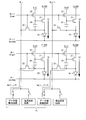
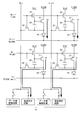
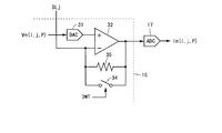
- FIG. 2 is a circuit diagram showing a part of the pixel circuit 20 and the data line drive / current measurement circuit 15.
- FIG. 2 shows a pixel circuit PX (i, j) in the i-th row and j-th column and a portion corresponding to the data line DLj in the data line driving / current measuring circuit 15.
- the pixel circuit 20 includes N-channel TFTs (Thin Film Transistors) 21 to 23, a capacitor 24, and an organic EL element 25.
- TFTs 21 to 23 TFTs having good off-leak characteristics are used.
- TFTs 21 to 23 for example, TFTs having a semiconductor layer formed of indium-gallium-zinc oxide (IGZO) are used.
- IGZO indium-gallium-zinc oxide
- the high level power supply voltage ELVDD is applied to the drain terminal of the TFT 21.
- the source terminal of the TFT 21 is connected to the anode terminal of the organic EL element 25, and the cathode terminal of the organic EL element 25 is connected to the power supply line PLi.
- One conduction terminal of the TFT 22 is connected to the data line DLj, and the other conduction terminal of the TFT 22 is connected to the source terminal of the TFT 21.
- a reference voltage Vref is applied to the drain terminal of the TFT 23, and the source terminal of the TFT 23 is connected to the gate terminal of the TFT 21.
- the gate terminal of the TFT 22 and the gate terminal of the TFT 23 are connected to the scanning line SLi.
- the capacitor 24 is provided between the gate terminal and the source terminal of the TFT 21.
- the organic EL element 25 is a current-driven light emitting element.
- the TFT 21 is provided in series with the organic EL element 25 and functions as a drive transistor that outputs a drive current in an amount corresponding to the gate-source voltage.
- the TFT 22 is provided between the source terminal of the TFT 21 and the data line DLj, and functions as an input / output transistor having a gate terminal connected to the scanning line SLi.
- the TFT 23 is provided between the wiring having the reference voltage Vref and the gate terminal of the TFT 21 and functions as a reference voltage application transistor having a gate terminal connected to the scanning line SLi.
- the capacitor 24 functions as a holding capacitor that holds the gate-source voltage of the TFT 21.
- the data line drive / current measurement circuit 15 includes a D / A converter 31, an operational amplifier 32, a capacitor 33, and a switch 34 corresponding to the data line DLj.
- a data voltage value Vm (i, j, P) included in the video signal D2 is applied to the input terminal of the D / A converter 31.
- the D / A converter 31 converts the data voltage value Vm (i, j, P) into an analog data voltage (represented as Vm (i, j, P) as with the data voltage value).
- the output terminal of the D / A converter 31 is connected to the non-inverting input terminal of the operational amplifier 32.
- the inverting input terminal of the operational amplifier 32 is connected to the data line DLj.
- the switch 34 is provided between the inverting input terminal and the output terminal of the operational amplifier 32.
- the capacitor 33 is provided between the inverting input terminal and the output terminal of the operational amplifier 32 in parallel with the switch 34.
- An input / output control signal DWT included in the control signal C3 is applied to the control terminal of the switch 34.
- the output terminal of the operational amplifier 32 is connected to the input terminal of the A / D converter 17.
- the switch 34 When the input / output control signal DWT is at a high level, the switch 34 is turned on, and the inverting input terminal and the output terminal of the operational amplifier 32 are short-circuited. At this time, the operational amplifier 32 functions as a buffer amplifier, and the data voltage Vm (i, j, P) given to the non-inverting input terminal of the operational amplifier 32 is applied to the data line DLj.
- the switch 34 When the input / output control signal DWT is at a low level, the switch 34 is turned off, and the inverting input terminal and the output terminal of the operational amplifier 32 are connected via the capacitor 33.
- the operational amplifier 32 and the capacitor 33 function as an integration circuit, and the output voltage of the operational amplifier 32 is a voltage corresponding to the drive current output from the pixel circuit 20 to the data line DLj.
- the A / D converter 17 converts the output voltage of the operational amplifier 32 into a digital value.
- the drive current measured by the data line drive / current measurement circuit 15 is referred to as Im (i, j, P)
- the digital value output from the A / D converter 17 is referred to as the drive current value.
- it is expressed as Im (i, j, P).
- the display device 10 performs rest driving that classifies the frame period into a driving period and a rest period.
- the display device 10 writes the display data voltage to the pixel circuit 20 during the driving period, and does not write the display data voltage to the pixel circuit 20 during the idle period. Further, the display device 10 measures the driving current output from the pixel circuits 20 for one row to the data lines DL1 to DLn during the idle period, and the correction data stored in the correction data storage unit 19 based on the driving current value. Update.
- the first gradation P1 and the second gradation P2 are determined in advance within the display gradation range.
- the data line drive / current measurement circuit 15 generates a first measurement voltage Vm (i, j, P1) for writing the first gradation P1 to the pixel circuit PX (i, j), and the first measurement voltage.
- the drive current output from the pixel circuit PX (i, j) in which Vm (i, j, P1) is written is measured as the first drive current Im (i, j, P1).
- the correction calculation circuit 18 uses the threshold voltage correction data Vt ( i, j) is updated.
- the data line drive / current measurement circuit 15 generates a second measurement voltage Vm (i, j, P2) for writing the second gradation P2 in the pixel circuit PX (i, j), and performs the second measurement.
- the drive current output from the pixel circuit PX (i, j) to which the working voltage Vm (i, j, P2) is written is measured as the second drive current Im (i, j, P2).
- the correction calculation circuit 18 uses the mobility correction data B (stored in the mobility correction data storage unit 48). i, j) is updated.
- the display device 10 performs pause driving in which the driving period and the pause period are alternately switched every frame period.
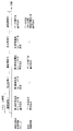
- FIG. 3 is a diagram illustrating operations of the display device 10 during a driving period and a rest period.
- the drive circuit of the display device 10 includes four consecutive frame periods F1 to F4 in a first drive period F1, a first pause period F2, a second drive period F3, and a second pause period.
- the frame period is classified as F4, and the next frame period after the second pause period F4 is classified as the third drive period F5.
- the display device 10 writes the first measurement voltage Vm (i, j, P1) to the pixel circuit PX (i, j) to be measured and displays the other pixel circuits for display.
- the display device 10 measures the first drive current Im (i, j, P1) output from the pixel circuit PX (i, j) to be measured.
- the display device 10 writes the second measurement voltage Vm (i, j, P2) to the pixel circuit PX (i, j) to be measured and displays the other pixel circuits for display. Write data voltage.
- the display device 10 measures the second drive current Im (i, j, P2) output from the pixel circuit PX (i, j) to be measured.
- the display device 10 writes the first measurement voltage to the next pixel circuit to be corrected, and displays the other measurement circuits (including the pixel circuit PX (i, j)). Write data voltage.
- the data voltage written to the pixel circuit PX (i, j) in the third driving period F5 is the first driving current value Im (i, j, P1) and the second driving current value Im (i, j, P2). Based on the corrected video signal D2 obtained by updating the two types of correction data stored in the correction data storage unit 19 and referring to the updated correction data.
- FIG. 4 is a timing chart of the driving period of the display device 10.
- the second scanning line driving circuit 14 stops operating.
- the first scanning line driving circuit 13 sequentially selects the scanning lines SL1 to SLm one line period at a time, and applies a selection voltage (here, a high level voltage) to the selected scanning line.
- the data line drive / current measurement circuit 15 applies n data voltages based on the corrected video signal D2 to the data lines DL1 to DLn, respectively. However, when the pixel circuit in the i-th row is the measurement target, the data line drive / current measurement circuit 15 applies the first measurement voltage Vm (i, i) to the data lines DL1 to DLn in the selection period of the scanning line SLi.
- the power supply voltage selection circuit 16 applies the first low level power supply voltage ELVSS to the power supply lines PL1 to PLm.
- the pixel circuits 20 for one row are sequentially selected for each line period, and the data voltage or the measurement voltage is written to the pixel circuits 20 in the selected row. Thereby, the data voltage or the measurement voltage can be written to all the pixel circuits 20 within one driving period.
- FIG. 5 is a timing chart of the pause period of the display device 10.
- the first scanning line driving circuit 13 stops operating.
- the second scanning line driving circuit 14 applies a selection voltage to the scanning line SLi over one frame period.
- the power supply voltage selection circuit 16 applies the second low level power supply voltage ELVSS_moni to the power supply line PLi and applies the first low level power supply voltage ELVSS to the other power supply lines.
- the data line drive / current measurement circuit 15 measures the drive current output from the pixel circuit 20 to be measured to the data lines DL1 to DLn. As a result, n drive currents output from the n pixel circuits 20 within one pause period can be measured.
- the data line drive / current measurement circuit 15 measures the first drive current Im (i, j, P1) in the first idle period F2, and the second drive current Im (i, j, P2) in the second idle period F4. Measure.
- the pixel circuit to be measured is switched every two pause periods. As a result, the two types of correction data stored in the correction data storage unit 19 for all the pixel circuits 20 can be updated within the 2m pause period.
- FIG. 6 is a diagram illustrating a voltage writing operation of the display device 10.
- the voltage writing operation for the pixel circuit PX (i, j) will be described.
- the voltage writing is performed within the driving period.
- the driving period the first low-level power supply voltage ELVSS is applied to the power supply line PLi.
- the selection period of the pixel circuit 20 in the i-th row the voltage of the scanning line SLi is at a high level, and the voltages of other scanning lines are at a low level (see FIG. 4).
- a data voltage Vm (i, j, P) for writing the gradation P to the pixel circuit PX (i, j) is applied to the data line DLj.
- the first measurement voltage Vm (i, j, P1) or the second measurement voltage Vm (i, j, P2) is applied to the data line DLj. Is done.
- the TFTs 22 and 23 are turned on. Therefore, the voltage of the data line DLj is applied to the source terminal of the TFT 21 via the TFT 22, and the reference voltage Vref is applied to the gate terminal of the TFT 21 via the TFT 23.
- a drive current Id flows between the drain and source of the TFT 21, and the organic EL element 25 emits light with a luminance corresponding to the drive current Id.
- the amount of the drive current Id and the luminance of the organic EL element 25 depend on the gate-source voltage Vgs of the TFT 21, the high level power supply voltage ELVDD, and the first low level power supply voltage ELVSS.
- the TFTs 22 and 23 are turned off. Thereafter, the gate-source voltage Vgs of the TFT 21 is maintained at the previous level by the action of the capacitor 24. Therefore, the organic EL element 25 continues to emit light with a luminance corresponding to the gate-source voltage Vgs of the TFT 21.
- FIG. 7 is a diagram illustrating a current measurement operation of the display device 10.
- the current measurement operation for the pixel circuit PX (i, j) will be described. Current measurements are made during the rest period.
- the voltage of the scanning line SLi is at a high level and the voltages of the other scanning lines are at a low level during the idle period (see FIG. 5).
- the second low level power supply voltage ELVSS_moni is applied to the power supply line PLi
- the first low level power supply voltage ELVSS is applied to the other power supply lines.
- the second low-level power supply voltage ELVSS_moni is determined so as to satisfy the following expression (1).
- the TFTs 22 and 23 are turned on. At this time, a drive current Id flows between the drain and source of the TFT 21.
- the amount of the drive current Id depends on the gate-source voltage Vgs of the TFT 21, the high-level power supply voltage ELVDD, and the second low-level power supply voltage ELVSS_moni. However, since Formula (1) is established, the drive current Id does not flow to the organic EL element 25 but flows to the data line drive / current measurement circuit 15 via the TFT 22 and the data line DLj.
- the data line drive / current measurement circuit 15 measures the drive current Id output from the pixel circuit PX (i, j), and uses the result as the first drive current Im (i, j, P1) or the second drive current Im. Output as (i, j, P2).
- the TFTs 22 and 23 are turned off.
- the state of the pixel circuit PX (i, j) does not change until the voltage of the scanning line SLi next changes to the high level.
- FIG. 8 is a block diagram showing details of the correction arithmetic circuit 18.
- the correction arithmetic circuit 18 includes a first LUT 41, a multiplier 42, an adder 43, a subtracter 44, a second LUT 45, and a CPU 46.
- reference symbol P represents a gradation included in the video signal D1.
- the correction arithmetic circuit 18 refers to the two types of correction data stored in the correction data storage unit 19 to correct the video signal D1 and the two drive current values output from the A / D converter 17. Based on this, an operation of updating two types of correction data stored in the correction data storage unit 19 is performed.
- the correction calculation circuit 18 functions as a correction circuit that corrects the video signal based on the drive current measured by the measurement circuit (data line drive / current measurement circuit 15).
- the CPU 46 may be constituted by an arithmetic circuit.
- the first LUT 41 stores an overdrive voltage Vc (P) corresponding to each gradation P for display.
- the first LUT 41 converts the gradation P included in the video signal D1 into an overdrive voltage Vc (P).
- the multiplier 42 multiplies the overdrive voltage Vc (P) and the mobility correction data B (i, j) read from the mobility correction data storage unit 48.
- the adder 43 adds the output of the multiplier 42 and the threshold voltage correction data Vt (i, j) read from the threshold voltage correction data storage unit 47.
- the subtracter 44 subtracts the output of the adder 43 from the value of the reference voltage Vref. Thereby, the correction calculation shown in the following equation (2) is performed on the gradation P included in the video signal D1.
- Vm (i, j, P) Vref ⁇ Vc (P) ⁇ B (i, j) ⁇ Vt (i, j) (2)
- the correction calculation circuit 18 outputs a corrected video signal D2 including the obtained data voltage value Vm (i, j, P).
- the data line drive / current measurement circuit 15 drives the data lines DL1 to DLn based on the corrected video signal D2.
- the second LUT 45 stores a first target current value I (P1) corresponding to the first gradation P1 and a second target current value I (P2) corresponding to the second gradation P2.
- the second LUT 45 outputs the first target current value I (P1) in the first pause period F2, and outputs the second target current value I (P2) in the second pause period F4.
- the CPU 46 receives the first drive current value Im (i, j, P1) from the A / D converter 17 in the first idle period F2, and the second drive current value from the A / D converter 17 in the second idle period F4. Im (i, j, P2) is received.
- the CPU 46 compares the first drive current value Im (i, j, P1) with the first target current value I (P1) and compares the result. Accordingly, the threshold voltage correction data Vt (i, j) stored in the threshold voltage correction data storage unit 47 is updated.
- the CPU 46 adds ⁇ V to the threshold voltage correction data Vt (i, j) when the following equation (3) holds, ⁇ V is subtracted from threshold voltage correction data Vt (i, j) when equation (4) is satisfied, and threshold voltage correction data Vt (i, j) is not updated when equation (5) is satisfied. .
- the first drive current value Im (i, j, P1) approaches the first target current value I (P1) stepwise, and finally converges to the first target current value I (P1).
- ⁇ V_dz (5)
- the CPU 46 When the CPU 46 receives the second drive current value Im (i, j, P2), the CPU 46 compares the second drive current value Im (i, j, P2) with the second target current value I (P2).
- the mobility correction data B (i, j) stored in the mobility correction data storage unit 48 is updated according to the comparison result. More specifically, when the update amount is ⁇ B and the dead zone width is B_dz, the CPU 46 adds ⁇ B to the mobility correction data B (i, j) when the following equation (6) is satisfied, If equation (7) holds, ⁇ B is subtracted from mobility correction data B (i, j). If equation (8) holds, mobility correction data B (i, j) is not updated. .
- the second drive current value Im (i, j, P2) approaches the second target current value I (P2) stepwise and finally converges to the second target current value I (P2).
- ⁇ B_dz (8)
- the initial value of the threshold voltage correction data Vt (i, j) is a predetermined voltage value, and the initial value of the mobility correction data B (i, j) is 1.
- the threshold voltage of the TFT 21 is Vt, and the gain of the TFT 21 is ⁇ .
- the amount of the drive current Id flowing between the drain and source of the TFT 21 is expressed by the following equation (9) using the gate-source voltage Vgs of the TFT 21.
- Id ⁇ / 2 ⁇ (Vgs-Vt) 2 (9)
- a reference voltage Vref is applied to the gate terminal of the TFT 21, and a data voltage Vm (i, j, P) is applied to the source terminal of the TFT 21.
- Formula (9) can be transformed into the following Formula (10).
- the threshold voltage correction data Vt (i, j) or the mobility correction data B (i, j) may be increased.
- the threshold voltage correction data Vt (i, j) or the mobility correction data B (i, j) may be reduced.
- FIG. 9 is a diagram showing the gradation-current characteristics of the display device 10.
- the CPU 46 updates the threshold voltage correction data Vt (i, j) and the mobility correction data B (i, j) by the above method. For this reason, the first drive current value Im (i, j, P1) and the second drive current value Im (i, j, P2) finally match the respective target values.
- the drive current when the first gradation P1 is written to the pixel circuit PX (i, j) and the drive current when the second gradation P2 is written to the pixel circuit PX (i, j) are: It matches each target amount.
- two black circles correspond to two white circles, respectively.
- the drive current when an arbitrary gradation P is written in the pixel circuit PX (i, j) substantially matches the target amount corresponding to the gradation P. Therefore, according to the display device 10, by correcting the threshold voltage and mobility of the TFT 21 for each pixel circuit 20, it is possible to perform high-quality display while suppressing luminance unevenness in the display screen.
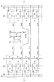
- FIG. 10 is a circuit diagram of the first scanning line driving circuit 13 and the second scanning line driving circuit 14.
- the first scanning line driving circuit 13 includes m flip-flops 51 connected in multiple stages.
- the flip-flop 51 has a reset terminal R, a clock terminal CK, an input terminal D, and an output terminal Q.
- a reset signal RST is supplied to the reset terminals R of the m flip-flops 51, and a clock signal CKa is supplied to the clock terminals CK of the m flip-flops 51.
- a control signal SDa is supplied to the input terminal D of the first-stage flip-flop 51.
- the input terminal D of the second and subsequent flip-flops 51 is connected to the output terminal Q of the preceding flip-flop 51.
- the output terminals Q of the m flip-flops 51 are connected to the scanning lines SL1 to SLm, respectively.
- the second scanning line driving circuit 14 includes m flip-flops 52 and m N-channel transistors 53 connected in multiple stages.
- a reset signal RST is supplied to the reset terminals R of the m flip-flops 52, and a clock signal CKb is supplied to the clock terminals CK of the m flip-flops 52.
- a control signal SDb is supplied to the input terminal D of the first-stage flip-flop 52.
- the input terminal D of the second and subsequent flip-flops 52 is connected to the output terminal Q of the preceding flip-flop 52.
- the m transistors 53 are provided between the output terminals Q of the m flip-flops 52 and the scanning lines SL1 to SLm, respectively.
- a control signal CX included in the control signal C2 is supplied to the control terminals of the m transistors 53.
- FIG. 11 is a timing chart of the first scanning line driving circuit 13.
- the clock signal CKa is a clock signal with a period of one line period.
- the control signal SDa becomes high level for one line period at the beginning of the frame period.
- the output signal SLa1 of the first-stage flip-flop 51 is at the high level.
- the output signal SLa2 of the second-stage flip-flop 51 becomes high level.
- the output signals SLa3, SLa4,... Of the flip-flops 51 in the third and subsequent stages sequentially become high level for each line period.
- the output signals SLa1 to SLam are applied to the scanning lines SL1 to SLm, respectively.
- FIG. 12 is a timing chart of the second scanning line driving circuit 14.
- the control signal CX is at a low level during the driving period and is at a high level during the pause period.
- the clock signal CKb is a clock signal having a period of 4 frame periods, and becomes high level for a predetermined time at the beginning of the driving period.
- the control signal SDb becomes high level for four frame periods before the pixel circuit 20 in the first row is set as a measurement target. In the next four frame periods after the four frame period in which the control signal SDb is at the high level, the output signal FF1_Q of the first-stage flip-flop 52 is at the high level.
- the output signal FF2_Q of the second-stage flip-flop 52 becomes high level.
- the output signals FF3_Q, FF4_Q,... Of the third and subsequent flip-flops 52 sequentially become high level every four frame periods.
- the m transistors 53 When the control signal CX is at a high level, the m transistors 53 are turned on, and the output signals FF1_Q to FFm_Q of the m flip-flops 52 become the output signals SLb1 to SLbm of the second scanning line driving circuit 14.
- the control signal CX When the control signal CX is at a low level, the m transistors 53 are turned off, and the output signals SLb1 to SLbm of the second scanning line driving circuit 14 are at a low level.
- the output signal SLb1 becomes high level when the output signal of the first-stage flip-flop 52 and the control signal CX are high level.
- the output signal SLb2 becomes high level after 4 frame periods of the high level period of the output signal SLb1.
- the output signal SLbi becomes a high level after four frame periods of the high level period of the output signal SLbi-1.
- FIG. 13 is a circuit diagram of the power supply voltage selection circuit 16.
- the power supply voltage selection circuit 16 includes a P-channel transistor 54 and an N-channel transistor 55 corresponding to the power supply line PLi.
- the first low level power supply voltage ELVSS is applied to the source terminal of the transistor 54
- the second low level power supply voltage ELVSS_moni is applied to the source terminal of the transistor 55.
- the drain terminals of the transistors 54 and 55 are connected to the power supply line PLi.
- the output signal SLbi of the second scanning line driving circuit 14 is supplied to the gate terminals of the transistors 54 and 55.
- the output signal SLbi is at a high level during the rest period and when the pixel circuit 20 in the i-th row is the measurement target, and at a low level otherwise.
- the output signal SLbi is at a high level, so that the transistor 54 is turned off and the transistor 55 is turned on.
- the second low-level power supply voltage ELVSS_moni is applied to the power supply line PLi via the transistor 55.
- the output signal SLbi is at a low level, so that the transistor 54 is turned on and the transistor 55 is turned off.
- the first low-level power supply voltage ELVSS is applied to the power supply line PLi via the transistor 54.
- the display device according to the comparative example (the display device that drives the scanning lines at the timing shown in FIG. 18) sufficiently suppresses uneven luminance in the display screen, which makes the configuration of the scanning line driving circuit complicated. There is a problem that power consumption at peak time is not possible.
- the display device 10 classifies the frame period into a driving period and a rest period, and measures a driving current in the rest period.
- the scanning line driving circuit of the display device 10 sequentially applies a selection voltage to the scanning lines SL1 to SLm in the driving period, and applies a selection voltage to one scanning line SLi corresponding to the pixel circuit to be measured in the pause period ( (See FIGS. 4 and 5).
- Such a scanning line driving circuit can be easily configured using the first scanning line driving circuit 13 and the second scanning line driving circuit 14 (see FIG. 10). Therefore, according to the display device 10, the configuration of the scanning line driving circuit can be simplified as compared with the display device according to the comparative example.
- the display device 10 since the drive current is measured in the idle period, a sufficient time can be secured for the drive current measurement. In the longest case, the drive current may be measured over one frame period. The longer the drive current measurement time, the more accurately the drive current can be measured, so that the characteristics (threshold voltage and mobility) of the TFT 21 can be compensated more effectively. Therefore, according to the display device 10, it is possible to effectively compensate for variations in the characteristics of the TFTs 21 compared to the display device according to the comparative example, and to effectively suppress luminance unevenness in the display screen.
- the display device 10 voltage writing and driving current measurement are performed in different frame periods. Therefore, according to the display device 10, the power consumption at the peak time can be reduced as compared with the display device according to the comparative example.
- the display device 10 includes (m ⁇ n) pixel circuits 20 and a drive circuit (a first scan line drive circuit 13 and a second scan line) that writes a voltage to the pixel circuit 20.
- Drive circuit 14 and data line drive / current measurement circuit 15 ), a measurement circuit (data line drive / current measurement circuit 15) for measuring the drive current output from the pixel circuit 20, and a drive measured by the measurement circuit.
- a correction circuit (correction calculation circuit 18) for correcting the video signal based on the current.
- the drive circuit classifies the frame period into a drive period and a pause period, and in the drive period, a selection voltage is sequentially applied to the scanning lines SL1 to SLm, and a voltage written to the pixel circuit 20 (data voltage, first measurement voltage, or , The second measurement voltage) is sequentially applied to the data lines DL1 to DLn, and the selection voltage is applied to one scanning line SLi corresponding to the pixel circuit 20 to be measured in the rest period.
- the measurement circuit measures the drive current output from the pixel circuit 20 to be measured in the idle period. Therefore, according to the display device 10, as described above, the configuration of the scanning line driving circuit can be simplified, luminance unevenness in the display screen can be effectively suppressed, and peak power consumption can be reduced.
- the driving circuit applies a voltage corresponding to the corrected video signal D2 to the data lines DL1 to DLn in the scanning line selection period corresponding to the pixel circuit 20 that is not the measurement target in the driving period, In the selection period of the scanning line SLi corresponding to the pixel circuit 20 to be measured, the first or second measurement voltage is applied to the data lines DL1 to DLn. In this way, by writing the measurement voltage to the pixel circuit to be measured in the drive period, the drive current output from the pixel circuit to which the measurement voltage is written can be measured in the subsequent pause period.
- the drive circuit classifies the four frame periods in order into a first drive period, a first idle period, a second drive period, and a second idle period, and the pixel circuit 20 to be measured within the first drive period.
- the first measurement voltage is applied to the data line DLj during the selection period of the scanning line SLi corresponding to, and the second measurement voltage is selected during the selection period of the scanning line SLi corresponding to the pixel circuit 20 to be measured within the second drive period. Is applied to the data line DLj.
- the measurement circuit measures the drive current output from the pixel circuit 20 to be measured as the first drive current in the first pause period, and the second drive current output from the pixel circuit 20 to be measured in the second pause period. Measured as drive current.
- the correction circuit corrects a part related to the pixel circuit 20 to be measured in the video signal D1 based on the first and second drive currents. In this manner, writing of the measurement voltage and measurement of the drive current are performed twice for the pixel circuit to be measured within the four frame period, and the video signal is corrected based on the two measurement results, thereby correcting the drive transistor. It is possible to compensate for variations in two types of characteristics (threshold voltage and mobility), and to effectively suppress luminance unevenness in the display screen.
- the driving circuit applies a selection voltage to one scanning line SLi corresponding to the pixel circuit 20 to be measured in one pause period. Accordingly, it is possible to compensate for variations in the characteristics of the driving transistors for a plurality of pixel circuits connected to one scanning line in one pause period.
- the display device 10 also includes a storage unit (correction data storage unit 19) that stores first and second correction data (threshold voltage correction data and mobility correction data) used for correcting the video signal for each pixel circuit 20.
- the correction circuit updates the first correction data related to the pixel circuit 20 to be measured based on the first drive current, updates the second correction data related to the pixel circuit 20 to be measured based on the second drive current, and 2.
- the portion of the video signal D1 related to the pixel circuit 20 to be measured is corrected.
- two correction data are stored for each pixel circuit, two correction data are updated based on the two measurement results, and the video signal is corrected based on the two correction data. It is possible to compensate for variations in two types of characteristics and effectively suppress luminance unevenness in the display screen.
- the drive circuit includes a first scan line drive circuit 13 that drives the scan lines SL1 to SLm in the drive period, and a second scan line drive circuit 14 that drives the scan lines SL1 to SLm in the idle period.
- the drive circuit and the measurement circuit share a drive / measurement circuit (an operational amplifier 32, a capacitor 33, and a switch 34) provided corresponding to the data line DLj.
- a drive / measurement circuit an operational amplifier 32, a capacitor 33, and a switch 34
- the display device according to the second embodiment of the present invention has the same configuration as the display device 10 according to the first embodiment (see FIG. 1).
- the display device according to the first embodiment measures the first drive current in the first idle period F2, and measures the second drive current in the second idle period F4.
- the display device according to the present embodiment measures the first drive current and the second drive current within one idle period.
- the display device writes the display data voltage to all the pixel circuits 20 during the driving period. More specifically, in the driving period, the second scanning line driving circuit 14 stops operating.
- the first scanning line driving circuit 13 sequentially selects the scanning lines SL1 to SLm one line period at a time and applies a selection voltage to the selected scanning line (see FIG. 4).
- the data line drive / current measurement circuit 15 applies n data voltages based on the corrected video signal D2 to the data lines DL1 to DLn, respectively.
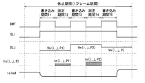
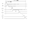
- FIG. 14 is a timing chart of the suspension period of the display device according to the present embodiment.
- the driving circuit of the display device according to the present embodiment sequentially includes a first writing period T1, a first measuring period T2, a second writing period T3, and a second measuring period T4 within one idle period. And a third writing period T5 is set.
- the second scanning line driving circuit 14 applies a selection voltage to the scanning line SLi in the periods T1 to T5. Note that in the pixel circuit 20 in the i-th row, the current Ioled flowing through the organic EL element 25 becomes zero during the periods T1 to T5.
- the input / output control signal DWT is at a high level, and the data line drive / current measurement circuit 15 functions as a data line drive circuit.
- the input / output control signal DWT is at a low level, and the data line drive / current measurement circuit 15 functions as a current measurement circuit.
- the data line drive / current measurement circuit 15 applies the first measurement voltage Vm (i, j, P1) to the data line DLj.
- the first measurement voltage Vm (i, j, P1) is written into the pixel circuit PX (i, j).
- the data line drive / current measurement circuit 15 measures the first drive current Im (i, j, P1) output from the pixel circuit PX (i, j) to the data line DLj.
- the CPU 46 updates the threshold voltage correction data Vt (i, j) stored in the threshold voltage correction data storage unit 47 based on the first drive current value Im (i, j, P1) at this time.
- the data line drive / current measurement circuit 15 applies the second measurement voltage Vm (i, j, P2) to the data line DLj.
- the second measurement voltage Vm (i, j, P2) is written into the pixel circuit PX (i, j).
- the data line drive / current measurement circuit 15 measures the second drive current Im (i, j, P2) output from the pixel circuit PX (i, j) to the data line DLj.
- the CPU 46 updates the mobility correction data B (i, j) stored in the mobility correction data storage unit 48 based on the second drive current value Im (i, j, P2) at this time.
- the data line drive / current measurement circuit 15 applies the data voltage Vm (i, j, P) to the data line DLj.
- the data voltage Vm (i, j, P) is written into the pixel circuit PX (i, j).
- the data voltage Vm (i, j, P) in the third writing period T5 is corrected based on the first drive current value Im (i, j, P1) and the second drive current value Im (i, j, P2). This is a voltage based on a corrected video signal D2 obtained by updating two types of correction data stored in the data storage unit 19 and referring to the updated correction data.
- the display device classifies the frame period into a drive period and an idle period, and measures the drive current in the idle period. Therefore, according to the display device according to the present embodiment, as in the first embodiment, the configuration of the scanning line driving circuit is simplified, the luminance unevenness in the display screen is effectively suppressed, and the power consumption at the peak time Can be reduced.
- the driving circuit applies a voltage corresponding to the corrected video signal D2 to the data lines DL1 to DLn in the selection period of each scanning line in the driving period, and in the idle period.
- a writing period and a measurement period are set, and the first or second measurement voltage is applied to the data lines DL1 to DLn in the writing period.
- the measurement circuit measures the drive current output from the pixel circuit 20 to be measured in the measurement period. In this way, by writing the measurement voltage to the pixel circuit to be measured in the writing period within the pause period, the drive current output from the pixel circuit to which the measurement voltage is written can be measured in the subsequent measurement period. .
- the driving circuit sets a first writing period, a first measurement period, a second writing period, and a second rest period in order within the pause period, and the first measurement voltage is set to the data line DLj in the first write period.
- the second measurement voltage is applied to the data line DLj in the second writing period.
- the measurement circuit measures the drive current output from the pixel circuit 20 to be measured as the first drive current in the first measurement period, and the second drive current output from the pixel circuit 20 to be measured in the second measurement period. Measured as drive current.
- the correction circuit corrects a part related to the pixel circuit 20 to be measured in the video signal D1 based on the first and second drive currents.
- the measurement voltage is written to the pixel circuit to be measured and the drive current is measured twice in one frame period, and the video signal is corrected based on the two measurement results. It is possible to compensate for variations in two types of characteristics (threshold voltage and mobility), and to effectively suppress luminance unevenness in the display screen.
- the driving circuit sets a third writing period after the second measurement period within the pause period, and applies a voltage corresponding to the corrected video signal D2 to the data lines DL1 to DLn in the third writing period.
- the voltage corresponding to the video signal corrected based on the measurement results in the first and second measurement periods is written in the pixel circuit to be measured in the third writing period, thereby compensating the variation in the characteristics of the driving transistor. Can be immediately reflected in the display image.
- the display device according to the third embodiment of the present invention has the same configuration as the display device 10 according to the first embodiment (see FIG. 1).
- the display device according to the first embodiment alternately switches between the driving period and the rest period.
- the display device according to the present embodiment treats a plurality of continuous pause periods as continuous pause periods, and alternately switches between a drive period and a continuous pause period.
- FIG. 15 is a diagram illustrating an operation in a driving period and a continuous rest period of the display device according to the embodiment.
- the drive circuit of the display device according to the present embodiment includes a plurality of frame periods in order of a first drive period F1, a first continuous pause period FS2, a second drive period F3, and a second continuous pause period FS4.
- the first and second continuous pause periods FS2 and FS4 are each composed of N pause periods (N is an integer of 2 or more).
- the display device according to the present embodiment performs the same operation on all the pixel circuits 20 in the periods F1, FS2, F3, FS4, and F5.
- the display device In the first driving period F1, the display device according to the present embodiment writes a display data voltage in the pixel circuit PX (i, j). In the first continuous rest period FS2, the display device according to the present embodiment writes the first measurement voltage Vm (i, j, P1) to the pixel circuit PX (i, j), and the pixel circuit PX (i, j). The first drive current Im (i, j, P1) output from is measured. In the second drive period F3, the display device according to the present embodiment writes a display data voltage in the pixel circuit PX (i, j).
- the display device In the second continuous rest period FS4, the display device according to the present embodiment writes the second measurement voltage Vm (i, j, P2) to the pixel circuit PX (i, j), and the pixel circuit PX (i, j). The second drive current Im (i, j, P2) output from is measured.
- the display device In the third drive period F5, the display device according to the present embodiment writes a display data voltage in the pixel circuit PX (i, j).
- the display device writes the display data voltage to all the pixel circuits 20 during the driving period, as in the second embodiment.
- FIG. 16 is a timing chart of the continuous pause period of the display device according to the present embodiment.
- the drive circuit of the display device according to the present embodiment sets m selection periods within one continuous pause period, and sets a writing period Tw and a measurement period Tm within each selection period. To do.
- the second scanning line driving circuit 14 applies a selection voltage to the scanning line SLi in the i-th selection period within the continuous pause period.
- the input / output control signal DWT becomes high level, and the data line drive / current
- the measurement circuit 15 functions as a data line driving circuit.
- the input / output control signal DWT is at a low level, and the data line drive / current measurement circuit 15 functions as a current measurement circuit.
- the data line driving / current measuring circuit 15 applies the display data voltage Vm (i, j, P) to the data line DLj.
- the data voltage Vm (i, j, P) is written into the pixel circuit PX (i, j).
- the data line drive / current measurement circuit 15 applies the first measurement voltage Vm (i, j, P1) to the data line DLj. To do.
- the first measurement voltage Vm (i, j, P1) is written into the pixel circuit PX (i, j).
- the data line drive / current measurement circuit 15 measures the first drive current Im (i, j, P1) output from the pixel circuit PX (i, j) to the data line DLj.
- the CPU 46 updates the threshold voltage correction data Vt (i, j) stored in the threshold voltage correction data storage unit 47 based on the first drive current value Im (i, j, P1) at this time.
- the data line driving / current measuring circuit 15 applies the display data voltage Vm (i, j, P) to the data line DLj.
- the data voltage Vm (i, j, P) is written into the pixel circuit PX (i, j).
- the data line drive / current measurement circuit 15 applies the second measurement voltage Vm (i, j, P2) to the data line DLj. To do.
- the second measurement voltage Vm (i, j, P2) is written into the pixel circuit PX (i, j).
- the data line drive / current measurement circuit 15 measures the second drive current Im (i, j, P2) output from the pixel circuit PX (i, j) to the data line DLj.
- the CPU 46 updates the mobility correction data B (i, j) stored in the mobility correction data storage unit 48 based on the second drive current value Im (i, j, P2) at this time.
- the data line drive / current measurement circuit 15 applies the display data voltage Vm (i, j, P) to the data line DLj.
- the data voltage Vm (i, j, P) is written into the pixel circuit PX (i, j).
- the data voltage Vm (i, j, P) in the third driving period F5 is corrected based on the first driving current value Im (i, j, P1) and the second driving current value Im (i, j, P2). This is a voltage based on a corrected video signal D2 obtained by updating two types of correction data stored in the data storage unit 19 and referring to the updated correction data.
- the display device classifies the frame period into a drive period and an idle period, and measures the drive current in the idle period. Therefore, according to the display device according to the present embodiment, similarly to the first and second embodiments, the configuration of the scanning line driving circuit is simplified, the luminance unevenness in the display screen is effectively suppressed, and the peak time is reached. Power consumption can be reduced.
- the driving circuit applies a voltage corresponding to the corrected video signal D2 to the data lines DL1 to DLn in the selection period of each scanning line in the driving period, and in the continuous pause period.
- a selection voltage is sequentially applied to the scanning lines SL1 to SLm, a writing period and a measurement period are set within the selection period of each scanning line, and the first or second measurement voltage is applied to the data line DLj in each writing period.
- the measurement circuit measures the drive current output from the pixel circuit 20 to be measured in each measurement period. In this manner, by writing the measurement voltage to the pixel circuit to be measured in each writing period within the continuous pause period, the drive current output from the pixel circuit having written the measurement voltage is measured in the subsequent measurement period. Can do.
- the driving circuit applies a selection voltage to all the scanning lines SL1 to SLm in order during one continuous pause period. Accordingly, it is possible to compensate for variations in the characteristics of the drive transistors for all the pixel circuits in one continuous pause period.
- the driving circuit applies the first measurement voltage to the data line DLj in each writing period within the first continuous pause period, and applies the second measurement voltage to the data line DLj in each write period within the second continuous pause period. Apply to.
- the measurement circuit measures the drive current output from the pixel circuit 20 to be measured as the first drive current in each measurement period within the first continuous pause period, and the measurement target in each measurement period within the second continuous pause period.
- the drive current output from the pixel circuit 20 is measured as the second drive current.
- the correction circuit corrects a part related to the circuit to be measured in the video signal D1 based on the first and second drive currents.
- the measurement voltage is written and the drive current is measured twice for all the pixel circuits within two continuous pause periods, and the video signal is corrected based on the two measurement results, thereby driving the pixel circuit. It is possible to compensate for variations in the two types of characteristics (threshold voltage and mobility) of the transistor and to effectively suppress luminance unevenness in the display screen.
- the pixel circuit 20 shown in FIG. 2 includes N-channel TFTs 21 to 23, the pixel circuit 20 may include P-channel TFTs.
- the polarity of the voltage applied to the pixel circuit 20 and the polarity of the voltage in the pixel circuit 20 are reversed.
- 2 includes the capacitor 33 between the inverting input terminal and the output terminal of the operational amplifier 32 in parallel with the switch 34
- the data line drive / current measurement circuit 15 includes:
- a resistor 35 may be included instead of the capacitor 33 (see FIG. 17).
- the switch 34 is off, the operational amplifier 32 and the resistor 35 function as an integration circuit.
- either a capacitive element or a resistive element may be provided as a passive element between the inverting input terminal and the output terminal of the operational amplifier.
- the driving circuit may sequentially apply the selection voltage to a plurality of scanning lines corresponding to the pixel circuit to be measured in one pause period. Accordingly, it is possible to compensate for variations in the characteristics of the driving transistors for a plurality of pixel circuits connected to a plurality of scanning lines in one pause period.
- the driving circuit may sequentially apply the selection voltage to a part of the scanning lines SL1 to SLm in one continuous pause period.
- the classification of the frame periods shown in FIGS. 3 and 15 is an example of a classification method
- the setting of the writing period and the measurement period within the pause period shown in FIG. 14 is an example of a setting method.
- the drive circuit of the display device according to the first embodiment may classify the frame period into a drive period and a pause period in a manner other than that shown in FIG.
- the drive circuit of the display device according to the second embodiment may set the writing period and the measurement period within the pause period in a mode other than that shown in FIG.
- the drive circuit of the display device according to the third embodiment may classify the frame period into a drive period and a continuous pause period in a manner other than that shown in FIG.
- the display device and the driving method thereof according to the present invention have a scan line driving circuit with a simple configuration, can effectively suppress luminance unevenness, and have low power consumption, such as an organic EL element.
- the present invention can be used for a display device including a current-driven light emitting element.
Landscapes
- Engineering & Computer Science (AREA)
- Physics & Mathematics (AREA)
- Computer Hardware Design (AREA)
- General Physics & Mathematics (AREA)
- Theoretical Computer Science (AREA)
- Control Of Indicators Other Than Cathode Ray Tubes (AREA)
- Control Of El Displays (AREA)
Abstract
駆動回路は、フレーム期間を駆動期間と休止期間に分類し、駆動期間では複数の走査線に順に選択電圧を印加すると共に、映像信号に応じた電圧(測定対象の場合には、測定用電圧)を複数のデータ線に順に印加する。休止期間では、駆動回路は測定対象の画素回路に対応した1本の走査線に選択電圧を印加し、測定回路は測定対象の画素回路から複数のデータ線に出力された駆動電流を測定する。駆動回路は休止期間内に書き込み期間と測定期間を設定し、書き込み期間では測定用電圧を複数のデータ線に印加し、測定回路は測定期間において測定対象の画素回路から複数のデータ線に出力された駆動電流を測定してもよい。これにより、簡単な構成の走査線駆動回路を有し、輝度むらを効果的に抑制できる低消費電力の表示装置を提供する。
Description
本発明は、表示装置に関し、特に、有機EL素子などの電流駆動型の発光素子を備えた表示装置およびその駆動方法に関する。
近年、薄型、軽量、高速応答可能な表示装置として、有機EL(Electro Luminescence)表示装置が注目されている。有機EL表示装置は、2次元状に配置された複数の画素回路を備えている。有機EL表示装置の画素回路は、有機EL素子と駆動トランジスタを含んでいる。駆動トランジスタは、有機EL素子と直列に設けられ、有機EL素子に流れる電流(以下、駆動電流という)の量を制御する。有機EL素子は、駆動電流の量に応じた輝度で発光する。
有機EL表示装置では、駆動トランジスタの特性(閾値電圧と移動度)にばらつきが発生する。駆動トランジスタの特性にばらつきが発生すると、駆動電流の量にばらつきが発生し、表示画面に輝度むらが発生する。このため、有機EL表示装置において表示画面内の輝度むらを抑制して高画質表示を行うためには、駆動トランジスタの特性のばらつきを補償する必要がある。
駆動トランジスタの特性のばらつきを補償する有機EL表示装置は、従来から各種知られている。例えば、特許文献1には、駆動電流を電源線経由で外部に読み出し、測定した駆動電流の量に基づき補正用ゲインと補正用オフセットを更新し、これらを用いて映像信号を補正する有機EL表示装置が記載されている。特許文献2には、駆動電流をデータ線経由で外部に読み出し、測定した駆動電流の量と目標量との比較結果に基づき駆動トランジスタの閾値電圧を更新し、これを用いて映像信号を補正する有機EL表示装置が記載されている。
これとは別に、低消費電力の表示装置として、休止駆動(間欠駆動、あるいは、低周波駆動とも呼ばれる)を行う表示装置が知られている。休止駆動とは、同じ画像を続けて表示するときに、フレーム期間を駆動期間と休止期間に分類し、駆動期間では駆動回路を動作させ、休止期間では駆動回路の動作を停止させる駆動方法である。休止駆動は、画素回路内のトランジスタのオフリーク特性が良い(オフリーク電流が小さい)場合に適用できる。休止駆動を行う表示装置は、例えば、特許文献3に記載されている。
以下、駆動トランジスタの特性のばらつきを補償するために、駆動電流をデータ線経由で外部に読み出す有機EL表示装置に着目する。また、比較例に係る表示装置として、1フレーム期間内に、すべての行の画素回路に対して映像信号に応じた電圧(以下、データ電圧という)を書き込むと共に、1行分の画素回路から出力された駆動電流を測定する表示装置を考える。以下、駆動電流を測定する画素回路を測定対象の画素回路という。
図18は、比較例に係る表示装置のタイミングチャートである。図18には、i行目の画素回路が測定対象である場合の走査線SL1~SLmの電圧の変化が記載されている。図18に示すように、1~m行目の画素回路にデータ電圧を順に書き込むために、走査線SL1~SLmの電圧は1ライン期間ずつ(時間Ts1ずつ)順にハイレベルに制御される。ただし、i行目の画素回路についてはデータ電圧の書き込みと駆動電流の測定を行うために、走査線SLiの電圧は時間Ts2(>Ts1)だけハイレベルに制御される。時間Ts2は、例えば、時間Ts1の数倍程度である。このように比較例に係る表示装置では、測定対象の画素回路に対応した走査線SLiの選択期間は、他の走査線の選択期間よりも長くなる。また、選択期間が他の走査線よりも長い走査線はフレーム期間ごとに切り替わる。
表示装置の走査線駆動回路は、一般に、フリップフロップを多段接続し、各段のフリップフロップのクロック端子にクロック信号を供給し、初段のフリップフロップの入力端子にスタートパルスを供給することにより構成される。しかし、比較例に係る表示装置の走査線駆動回路は、走査線の電圧を図18に示すように制御する必要がある。このため、比較例に係る表示装置では、一般的な表示装置よりも走査線駆動回路の構成が複雑になる。
また、駆動電流はμAオーダー以下の微小電流であるので、駆動電流を正確に測定するためには測定時間を長くする必要がある。しかし、比較例に係る表示装置では、1フレーム期間内にすべての行の画素回路にデータ電圧を書き込むので、駆動電流の測定に十分な時間を確保できない。このため、比較例に係る表示装置には、駆動トランジスタの特性のばらつきを十分に補償できず、表示画面内の輝度むらを十分に抑制できないという問題がある。また、比較例に係る表示装置には、データ電圧の書き込みと駆動電流の測定を同じフレーム期間で行うので、ピーク時の消費電力が大きいという問題もある。
それ故に、本発明は、簡単な構成の走査線駆動回路を有し、輝度むらを効果的に抑制できる低消費電力の表示装置、および、その駆動方法を提供することを目的とする。
本発明の第1の局面は、電流駆動型の発光素子を備えた表示装置であって、
複数の走査線と複数のデータ線の交差点に対応して配置された複数の画素回路と、
前記走査線と前記データ線を駆動することにより、前記画素回路に電圧を書き込む駆動回路と、
前記画素回路から前記データ線に出力された駆動電流を測定する測定回路と、
前記測定回路で測定された駆動電流に基づき、映像信号を補正する補正回路とを備え、
前記画素回路は、
発光素子と、
前記発光素子と直列に設けられ、制御端子と前記発光素子側の導通端子との間の電圧に応じた量の駆動電流を出力する駆動トランジスタと、
前記駆動トランジスタの前記発光素子側の導通端子と前記データ線との間に設けられ、前記走査線に接続された制御端子を有する入出力トランジスタとを含み、
前記駆動回路は、フレーム期間を駆動期間と休止期間に分類し、駆動期間では前記走査線に順に選択電圧を印加すると共に、前記画素回路に書き込む電圧を前記データ線に順に印加し、休止期間では測定対象の画素回路に対応した1本以上の走査線に前記選択電圧を印加し、
前記測定回路は、休止期間において、測定対象の画素回路から出力された駆動電流を測定することを特徴とする。
複数の走査線と複数のデータ線の交差点に対応して配置された複数の画素回路と、
前記走査線と前記データ線を駆動することにより、前記画素回路に電圧を書き込む駆動回路と、
前記画素回路から前記データ線に出力された駆動電流を測定する測定回路と、
前記測定回路で測定された駆動電流に基づき、映像信号を補正する補正回路とを備え、
前記画素回路は、
発光素子と、
前記発光素子と直列に設けられ、制御端子と前記発光素子側の導通端子との間の電圧に応じた量の駆動電流を出力する駆動トランジスタと、
前記駆動トランジスタの前記発光素子側の導通端子と前記データ線との間に設けられ、前記走査線に接続された制御端子を有する入出力トランジスタとを含み、
前記駆動回路は、フレーム期間を駆動期間と休止期間に分類し、駆動期間では前記走査線に順に選択電圧を印加すると共に、前記画素回路に書き込む電圧を前記データ線に順に印加し、休止期間では測定対象の画素回路に対応した1本以上の走査線に前記選択電圧を印加し、
前記測定回路は、休止期間において、測定対象の画素回路から出力された駆動電流を測定することを特徴とする。
本発明の第2の局面は、本発明の第1の局面において、
前記駆動回路は、駆動期間内の測定対象ではない画素回路に対応した走査線の選択期間では補正後の映像信号に応じた電圧を前記データ線に印加し、駆動期間内の測定対象の画素回路に対応した走査線の選択期間では測定用電圧を前記データ線に印加することを特徴とする。
前記駆動回路は、駆動期間内の測定対象ではない画素回路に対応した走査線の選択期間では補正後の映像信号に応じた電圧を前記データ線に印加し、駆動期間内の測定対象の画素回路に対応した走査線の選択期間では測定用電圧を前記データ線に印加することを特徴とする。
本発明の第3の局面は、本発明の第2の局面において、
前記駆動回路は、4個のフレーム期間を順に第1駆動期間、第1休止期間、第2駆動期間、および、第2休止期間に分類し、第1駆動期間内の測定対象の画素回路に対応した走査線の選択期間では第1測定用電圧を前記データ線に印加し、第2駆動期間内の測定対象の画素回路に対応した走査線の選択期間では第2測定用電圧を前記データ線に印加し、
前記測定回路は、第1休止期間では測定対象の画素回路から出力された駆動電流を第1駆動電流として測定し、第2休止期間では測定対象の画素回路から出力された駆動電流を第2駆動電流として測定し、
前記補正回路は、前記第1および第2駆動電流に基づき、前記映像信号のうち測定対象の画素回路に関する部分を補正することを特徴とする。
前記駆動回路は、4個のフレーム期間を順に第1駆動期間、第1休止期間、第2駆動期間、および、第2休止期間に分類し、第1駆動期間内の測定対象の画素回路に対応した走査線の選択期間では第1測定用電圧を前記データ線に印加し、第2駆動期間内の測定対象の画素回路に対応した走査線の選択期間では第2測定用電圧を前記データ線に印加し、
前記測定回路は、第1休止期間では測定対象の画素回路から出力された駆動電流を第1駆動電流として測定し、第2休止期間では測定対象の画素回路から出力された駆動電流を第2駆動電流として測定し、
前記補正回路は、前記第1および第2駆動電流に基づき、前記映像信号のうち測定対象の画素回路に関する部分を補正することを特徴とする。
本発明の第4の局面は、本発明の第1の局面において、
前記駆動回路は、駆動期間内の各走査線の選択期間では補正後の映像信号に応じた電圧を前記データ線に印加し、休止期間内に書き込み期間と測定期間を設定し、書き込み期間では測定用電圧を前記データ線に印加し、
前記測定回路は、測定期間において、測定対象の画素回路から出力された駆動電流を測定することを特徴とする。
前記駆動回路は、駆動期間内の各走査線の選択期間では補正後の映像信号に応じた電圧を前記データ線に印加し、休止期間内に書き込み期間と測定期間を設定し、書き込み期間では測定用電圧を前記データ線に印加し、
前記測定回路は、測定期間において、測定対象の画素回路から出力された駆動電流を測定することを特徴とする。
本発明の第5の局面は、本発明の第4の局面において、
前記駆動回路は、休止期間内に順に第1書き込み期間、第1測定期間、第2書き込み期間、および、第2休止期間を設定し、第1書き込み期間では第1測定用電圧を前記データ線に印加し、第2書き込み期間では第2測定用電圧を前記データ線に印加し、
前記測定回路は、第1測定期間では測定対象の画素回路から出力された駆動電流を第1駆動電流として測定し、第2測定期間では測定対象の画素回路から出力された駆動電流を第2駆動電流として測定し、
前記補正回路は、前記第1および第2駆動電流に基づき、前記映像信号のうち測定対象の画素回路に関する部分を補正することを特徴とする。
前記駆動回路は、休止期間内に順に第1書き込み期間、第1測定期間、第2書き込み期間、および、第2休止期間を設定し、第1書き込み期間では第1測定用電圧を前記データ線に印加し、第2書き込み期間では第2測定用電圧を前記データ線に印加し、
前記測定回路は、第1測定期間では測定対象の画素回路から出力された駆動電流を第1駆動電流として測定し、第2測定期間では測定対象の画素回路から出力された駆動電流を第2駆動電流として測定し、
前記補正回路は、前記第1および第2駆動電流に基づき、前記映像信号のうち測定対象の画素回路に関する部分を補正することを特徴とする。
本発明の第6の局面は、本発明の第5の局面において、
前記駆動回路は、休止期間内で第2測定期間の後に第3書き込み期間を設定し、第3書き込み期間では補正後の映像信号に応じた電圧を前記データ線に印加することを特徴とする。
前記駆動回路は、休止期間内で第2測定期間の後に第3書き込み期間を設定し、第3書き込み期間では補正後の映像信号に応じた電圧を前記データ線に印加することを特徴とする。
本発明の第7の局面は、本発明の第2または第4の局面において、
前記駆動回路は、1個の休止期間において、測定対象の画素回路に対応した1本の走査線に前記選択電圧を印加することを特徴とする。
前記駆動回路は、1個の休止期間において、測定対象の画素回路に対応した1本の走査線に前記選択電圧を印加することを特徴とする。
本発明の第8の局面は、本発明の第2または第4の局面において、
前記駆動回路は、1個の休止期間において、測定対象の画素回路に対応した複数の走査線に順に前記選択電圧を印加することを特徴とする。
前記駆動回路は、1個の休止期間において、測定対象の画素回路に対応した複数の走査線に順に前記選択電圧を印加することを特徴とする。
本発明の第9の局面は、本発明の第1の局面において、
前記駆動回路は、駆動期間内の各走査線の選択期間では補正後の映像信号に応じた電圧を前記データ線に印加し、連続した複数の休止期間からなる連続休止期間において、前記走査線に順に前記選択電圧を印加すると共に、各走査線の選択期間内に書き込み期間と測定期間を設定し、各書き込み期間では測定用電圧を前記データ線に印加し、
前記測定回路は、各測定期間において、測定対象の画素回路から出力された駆動電流を測定することを特徴とする。
前記駆動回路は、駆動期間内の各走査線の選択期間では補正後の映像信号に応じた電圧を前記データ線に印加し、連続した複数の休止期間からなる連続休止期間において、前記走査線に順に前記選択電圧を印加すると共に、各走査線の選択期間内に書き込み期間と測定期間を設定し、各書き込み期間では測定用電圧を前記データ線に印加し、
前記測定回路は、各測定期間において、測定対象の画素回路から出力された駆動電流を測定することを特徴とする。
本発明の第10の局面は、本発明の第9の局面において、
前記駆動回路は、1個の連続休止期間において、すべての前記走査線に順に選択電圧を印加することを特徴とする。
前記駆動回路は、1個の連続休止期間において、すべての前記走査線に順に選択電圧を印加することを特徴とする。
本発明の第11の局面は、本発明の第10の局面において、
前記駆動回路は、第1連続休止期間内の各書き込み期間では第1測定用電圧を前記データ線に印加し、第2連続休止期間内の各書き込み期間では第2測定用電圧を前記データ線に印加し、
前記測定回路は、第1連続休止期間内の各測定期間では測定対象の画素回路から出力された駆動電流を第1駆動電流として測定し、第2連続休止期間内の各測定期間では測定対象の画素回路から出力された駆動電流を第2駆動電流として測定し、
前記補正回路は、前記第1および第2駆動電流に基づき、前記映像信号のうち測定対象の回路に関する部分を補正することを特徴とする。
前記駆動回路は、第1連続休止期間内の各書き込み期間では第1測定用電圧を前記データ線に印加し、第2連続休止期間内の各書き込み期間では第2測定用電圧を前記データ線に印加し、
前記測定回路は、第1連続休止期間内の各測定期間では測定対象の画素回路から出力された駆動電流を第1駆動電流として測定し、第2連続休止期間内の各測定期間では測定対象の画素回路から出力された駆動電流を第2駆動電流として測定し、
前記補正回路は、前記第1および第2駆動電流に基づき、前記映像信号のうち測定対象の回路に関する部分を補正することを特徴とする。
本発明の第12の局面は、本発明の第3、第5、および、第11のいずれかの局面において、
前記映像信号の補正に用いられる第1および第2補正データを前記画素回路ごとに記憶する記憶部をさらに備え、
前記補正回路は、前記第1駆動電流に基づき測定対象の画素回路に関する第1補正データを更新し、前記第2駆動電流に基づき測定対象の画素回路に関する第2補正データを更新し、前記第1および第2補正データに基づき、前記映像信号のうち測定対象の画素回路に関する部分を補正することを特徴とする。
前記映像信号の補正に用いられる第1および第2補正データを前記画素回路ごとに記憶する記憶部をさらに備え、
前記補正回路は、前記第1駆動電流に基づき測定対象の画素回路に関する第1補正データを更新し、前記第2駆動電流に基づき測定対象の画素回路に関する第2補正データを更新し、前記第1および第2補正データに基づき、前記映像信号のうち測定対象の画素回路に関する部分を補正することを特徴とする。
本発明の第13の局面は、本発明の第1の局面において、
前記駆動回路は、駆動期間において前記走査線を駆動する第1走査線駆動回路と、休止期間において前記走査線を駆動する第2走査線駆動回路とを含むことを特徴とする。
前記駆動回路は、駆動期間において前記走査線を駆動する第1走査線駆動回路と、休止期間において前記走査線を駆動する第2走査線駆動回路とを含むことを特徴とする。
本発明の第14の局面は、本発明の第1の局面において、
前記駆動回路と前記測定回路は、前記データ線に対応した駆動/測定回路を共有し、
前記駆動/測定回路は、前記データ線に接続された反転入力端子を有するオペアンプと、前記オペアンプの反転入力端子と出力端子との間に設けられたスイッチ素子と、前記スイッチ素子と並列に前記オペアンプの反転入力端子と出力端子との間に設けられた受動素子とを含み、
前記受動素子は、容量素子および抵抗素子のいずれかであることを特徴とする。
前記駆動回路と前記測定回路は、前記データ線に対応した駆動/測定回路を共有し、
前記駆動/測定回路は、前記データ線に接続された反転入力端子を有するオペアンプと、前記オペアンプの反転入力端子と出力端子との間に設けられたスイッチ素子と、前記スイッチ素子と並列に前記オペアンプの反転入力端子と出力端子との間に設けられた受動素子とを含み、
前記受動素子は、容量素子および抵抗素子のいずれかであることを特徴とする。
本発明の第15の局面は、複数の走査線と複数のデータ線の交差点に対応して配置され、それぞれが、電流駆動型の発光素子と、前記発光素子と直列に設けられ、制御端子と前記発光素子側の導通端子との間の電圧に応じた量の駆動電流を出力する駆動トランジスタと、前記駆動トランジスタの前記発光素子側の導通端子と前記データ線との間に設けられ、前記走査線に接続された制御端子を有する入出力トランジスタとを有する複数の画素回路を含む表示装置の駆動方法であって、
前記走査線と前記データ線を駆動することにより、前記画素回路に電圧を書き込む駆動ステップと、
前記画素回路から前記データ線に出力された駆動電流を測定する測定ステップと、
測定された駆動電流に基づき、映像信号を補正する補正ステップとを備え、
前記駆動ステップは、フレーム期間を駆動期間と休止期間に分類し、駆動期間では前記走査線に順に選択電圧を印加すると共に、前記画素回路に書き込む電圧を前記データ線に順に印加し、休止期間では測定対象の画素回路に対応した1本以上の走査線に前記選択電圧を印加し、
前記測定ステップは、休止期間において、測定対象の画素回路から出力された駆動電流を測定することを特徴とする。
前記走査線と前記データ線を駆動することにより、前記画素回路に電圧を書き込む駆動ステップと、
前記画素回路から前記データ線に出力された駆動電流を測定する測定ステップと、
測定された駆動電流に基づき、映像信号を補正する補正ステップとを備え、
前記駆動ステップは、フレーム期間を駆動期間と休止期間に分類し、駆動期間では前記走査線に順に選択電圧を印加すると共に、前記画素回路に書き込む電圧を前記データ線に順に印加し、休止期間では測定対象の画素回路に対応した1本以上の走査線に前記選択電圧を印加し、
前記測定ステップは、休止期間において、測定対象の画素回路から出力された駆動電流を測定することを特徴とする。
本発明の第1または第15の局面によれば、フレーム期間は駆動期間と休止期間に分類され、休止期間において測定対象の画素回路からデータ線に出力された駆動電流が測定される。駆動期間では複数の走査線に順に選択電圧を印加し、休止期間では1本以上の走査線に選択電圧を印加する走査線駆動回路は、簡単な構成を有する。また、休止期間において駆動電流を測定することにより、駆動電流の測定に十分な時間を確保し、駆動トランジスタの特性のばらつきを効果的に補償して、表示画面内の輝度むらを効果的に抑制することができる。また、電圧の書き込みと駆動電流の測定を異なるフレーム期間で行うことにより、ピーク時の消費電力を削減することができる。したがって、簡単な構成の走査線駆動回路を有し、輝度むらを効果的に抑制できる低消費電力の表示装置、または、その駆動方法を提供することができる。
本発明の第2の局面によれば、駆動期間において測定対象の画素回路に測定用電圧が書き込まれる。したがって、後続の休止期間において、測定用電圧を書き込んだ画素回路から出力される駆動電流を測定することができる。
本発明の第3の局面によれば、4フレーム期間内に測定対象の画素回路に対して測定用電圧の書き込みと駆動電流の測定が2回ずつ行われ、映像信号は2個の測定結果に基づき補正される。したがって、駆動トランジスタの2種類の特性(例えば、閾値電圧と移動度)のばらつきを補償し、表示画面内の輝度むらを効果的に抑制することができる。
本発明の第4の局面によれば、休止期間内の書き込み期間において測定対象の画素回路に測定用電圧が書き込まれる。したがって、後続の測定期間において、測定用電圧を書き込んだ画素回路から出力される駆動電流を測定することができる。
本発明の第5の局面によれば、1フレーム期間内に測定対象の画素回路に対して測定用電圧の書き込みと駆動電流の測定が2回ずつ行われ、映像信号は2個の測定結果に基づき補正される。したがって、駆動トランジスタの2種類の特性のばらつきを補償し、表示画面内の輝度むらを効果的に抑制することができる。
本発明の第6の局面によれば、第3書き込み期間において測定対象の画素回路には、第1および第2測定期間における測定結果に基づき補正された映像信号に応じた電圧が書き込まれる。したがって、駆動トランジスタの特性のばらつきを補償した結果を表示画像に直ちに反映することができる。
本発明の第7の局面によれば、1個の休止期間において、1本の走査線に接続された複数の画素回路について駆動トランジスタの特性のばらつきを補償することができる。
本発明の第8の局面によれば、1個の休止期間において、複数の走査線に接続された複数の画素回路について駆動トランジスタの特性のばらつきを補償することができる。
本発明の第9の局面によれば、連続休止期間内の各書き込み期間において測定対象の画素回路に測定用電圧が書き込まれる。したがって、後続の測定期間において、測定用電圧を書き込んだ画素回路から出力される駆動電流を測定することができる。
本発明の第10の局面によれば、1個の連続休止期間において、すべての画素回路について駆動トランジスタの特性のばらつきを補償することができる。
本発明の第11の局面によれば、2個の連続休止期間内にすべての画素回路に対して測定用電圧の書き込みと駆動電流の測定が2回ずつ行われ、映像信号は2個の測定結果に基づき補正される。したがって、駆動トランジスタの2種類の特性のばらつきを補償し、表示画面内の輝度むらを効果的に抑制することができる。
本発明の第12の局面によれば、画素回路ごとに2個の補正データを記憶し、2個の測定結果に基づき2個の補正データを更新し、2個の補正データに基づき映像信号を補正することにより、駆動トランジスタの2種類の特性のばらつきを補償し、表示画面内の輝度むらを効果的に抑制することができる。
本発明の第13の局面によれば、駆動期間で動作する回路と休止期間で動作する回路に分割することにより、走査線駆動回路を容易に構成することができる。
本発明の第14の局面によれば、駆動/測定回路は、スイッチ素子がオン状態のときにはオペアンプの非反転入力端子に与えられた電圧をデータ線に印加し、スイッチ素子がオフ状態のときにはデータ線に出力された駆動電流に応じた電圧をオペアンプの出力端子から出力する。したがって、駆動/測定回路を用いて、画素回路に電圧を書き込む駆動回路と画素回路からデータ線に出力された駆動電流を測定する測定回路とを容易に構成することができる。
(第1の実施形態)
図1は、本発明の第1の実施形態に係る表示装置の構成を示すブロック図である。図1に示す表示装置10は、表示部11、表示制御回路12、第1走査線駆動回路13、第2走査線駆動回路14、データ線駆動/電流測定回路15、電源電圧選択回路16、A/D変換器17、補正演算回路18、および、補正データ記憶部19を備えた有機EL表示装置である。以下、mおよびnは2以上の整数、iは1以上m以下の整数、jは1以上n以下の整数であるとする。
図1は、本発明の第1の実施形態に係る表示装置の構成を示すブロック図である。図1に示す表示装置10は、表示部11、表示制御回路12、第1走査線駆動回路13、第2走査線駆動回路14、データ線駆動/電流測定回路15、電源電圧選択回路16、A/D変換器17、補正演算回路18、および、補正データ記憶部19を備えた有機EL表示装置である。以下、mおよびnは2以上の整数、iは1以上m以下の整数、jは1以上n以下の整数であるとする。
表示部11は、m本の走査線SL1~SLm、n本のデータ線DL1~DLn、m本の電源線PL1~PLm、および、(m×n)個の画素回路20を含んでいる。走査線SL1~SLmと電源線PL1~PLmは、互いに平行に配置される。データ線DL1~DLnは、走査線SL1~SLmと直交するように互いに平行に配置される。走査線SL1~SLmとデータ線DL1~DLnは、(m×n)カ所で交差する。(m×n)個の画素回路20は、走査線SL1~SLmとデータ線DL1~DLnの交差点に対応して配置される。以下、走査線SL1~SLmの延伸方向(図1では、水平方向)を行方向、データ線DL1~DLnの延伸方向(図1では、垂直方向)を列方向といい、i行j列目の画素回路20をPX(i,j)という。
第1走査線駆動回路13は、表示部11の一辺(図1では右辺)に沿って配置される。第2走査線駆動回路14と電源電圧選択回路16は、表示部11の対向する辺(図1では左辺)に沿って配置される。データ線駆動/電流測定回路15は、表示部11の残余の一辺(図1では下辺)に沿って配置される。
表示制御回路12は、表示装置10の動作を制御するために制御信号を出力する。より詳細には、表示制御回路12は、第1走査線駆動回路13に対して制御信号C1を出力し、第2走査線駆動回路14に対して制御信号C2を出力し、データ線駆動/電流測定回路15に対して制御信号C3を出力する。また、表示制御回路12は、補正演算回路18に対して映像信号D1(補正前の映像信号)を出力する。
第1走査線駆動回路13と第2走査線駆動回路14は、走査線SL1~SLmを駆動する。データ線駆動/電流測定回路15は、データ線DL1~DLnを駆動する動作と、画素回路20からデータ線DL1~DLnに出力された駆動電流を測定する動作とを選択的に行う。第1走査線駆動回路13、第2走査線駆動回路14、および、データ線駆動/電流測定回路15は、走査線SL1~SLmとデータ線DL1~DLnを駆動することにより、画素回路20に電圧を書き込む駆動回路として機能する。データ線駆動/電流測定回路15は、画素回路20からデータ線DL1~DLnに出力された駆動電流を測定する測定回路としても機能する。電源電圧選択回路16は、電源線PL1~PLmに対して、表示用の第1ローレベル電源電圧ELVSSと電流測定用の第2ローレベル電源電圧ELVSS_moniとを選択的に印加する。各画素回路20には、図示しない電源回路からハイレベル電源電圧ELVDDと基準電圧Vrefが供給される。
補正データ記憶部19は、映像信号D1の補正に使用される2種類の補正データを記憶している。より詳細には、補正データ記憶部19は、閾値電圧補正データ記憶部47と移動度補正データ記憶部48を含んでいる。閾値電圧補正データ記憶部47は、画素回路PX(i,j)ごとに閾値電圧補正データVt(i,j)を記憶している。移動度補正データ記憶部48は、画素回路PX(i,j)ごとに移動度補正データB(i,j)を記憶している。
データ線駆動/電流測定回路15は、画素回路20からデータ線DL1~DLnに出力された駆動電流に応じた電圧を出力する。A/D変換器17は、データ線駆動/電流測定回路15から出力された電圧をデジタル値に変換する。このデジタル値は、画素回路20から出力された駆動電流の量を表す。補正演算回路18は、A/D変換器17から出力されたデジタル値に基づき、補正データ記憶部19に記憶された補正データを更新する。また、補正演算回路18は、補正データ記憶部19に記憶された補正データを参照して映像信号D1を補正し、補正後の映像信号D2を出力する。データ線駆動/電流測定回路15は、補正後の映像信号D2に基づきデータ線DL1~DLnを駆動する。
図2は、画素回路20とデータ線駆動/電流測定回路15の一部を示す回路図である。図2には、i行j列目の画素回路PX(i,j)と、データ線駆動/電流測定回路15のうちデータ線DLjに対応した部分とが記載されている。図2に示すように、画素回路20は、Nチャネル型のTFT(Thin Film Transistor)21~23、コンデンサ24、および、有機EL素子25を含んでいる。TFT21~23には、オフリーク特性が良いTFTが使用される。TFT21~23には、例えば、インジウム-ガリウム-亜鉛酸化物(IGZO)で形成された半導体層を有するTFTが使用される。
TFT21のドレイン端子には、ハイレベル電源電圧ELVDDが印加される。TFT21のソース端子は有機EL素子25のアノード端子に接続され、有機EL素子25のカソード端子は電源線PLiに接続される。TFT22の一方の導通端子はデータ線DLjに接続され、TFT22の他方の導通端子はTFT21のソース端子に接続される。TFT23のドレイン端子には基準電圧Vrefが印加され、TFT23のソース端子はTFT21のゲート端子に接続される。TFT22のゲート端子とTFT23のゲート端子は、走査線SLiに接続される。コンデンサ24は、TFT21のゲート端子とソース端子の間に設けられる。
有機EL素子25は、電流駆動型の発光素子である。TFT21は、有機EL素子25と直列に設けられ、ゲート-ソース間電圧に応じた量の駆動電流を出力する駆動トランジスタとして機能する。TFT22は、TFT21のソース端子とデータ線DLjの間に設けられ、走査線SLiに接続されたゲート端子を有する入出力トランジスタとして機能する。TFT23は、基準電圧Vrefを有する配線とTFT21のゲート端子の間に設けられ、走査線SLiに接続されたゲート端子を有する基準電圧印加トランジスタとして機能する。コンデンサ24は、TFT21のゲート-ソース間電圧を保持する保持容量として機能する。
データ線駆動/電流測定回路15は、データ線DLjに対応して、D/A変換器31、オペアンプ32、コンデンサ33、および、スイッチ34を含んでいる。D/A変換器31の入力端子には、映像信号D2に含まれるデータ電圧値Vm(i,j,P)が与えられる。D/A変換器31は、データ電圧値Vm(i,j,P)をアナログのデータ電圧(データ電圧値と同じくVm(i,j,P)と表す)に変換する。D/A変換器31の出力端子は、オペアンプ32の非反転入力端子に接続される。オペアンプ32の反転入力端子は、データ線DLjに接続される。スイッチ34は、オペアンプ32の反転入力端子と出力端子の間に設けられる。コンデンサ33は、スイッチ34と並列にオペアンプ32の反転入力端子と出力端子の間に設けられる。スイッチ34の制御端子には、制御信号C3に含まれる入出力制御信号DWTが与えられる。オペアンプ32の出力端子は、A/D変換器17の入力端子に接続される。
入出力制御信号DWTがハイレベルのときには、スイッチ34はオン状態になり、オペアンプ32の反転入力端子と出力端子は短絡される。このとき、オペアンプ32はバッファアンプとして機能し、データ線DLjにはオペアンプ32の非反転入力端子に与えられたデータ電圧Vm(i,j,P)が印加される。入出力制御信号DWTがローレベルのときには、スイッチ34はオフ状態になり、オペアンプ32の反転入力端子と出力端子はコンデンサ33を介して接続される。このとき、オペアンプ32とコンデンサ33は積分回路として機能し、オペアンプ32の出力電圧は画素回路20からデータ線DLjに出力された駆動電流に応じた電圧となる。A/D変換器17は、オペアンプ32の出力電圧をデジタル値に変換する。以下、データ線駆動/電流測定回路15で測定された駆動電流をIm(i,j,P)といい、A/D変換器17から出力されたデジタル値を駆動電流値といい、駆動電流と同じくIm(i,j,P)と表す。
表示装置10は、フレーム期間を駆動期間と休止期間に分類する休止駆動を行う。表示装置10は、駆動期間では画素回路20に表示用のデータ電圧を書き込み、休止期間では画素回路20に表示用のデータ電圧を書き込まない。また、表示装置10は、休止期間において、1行分の画素回路20からデータ線DL1~DLnに出力された駆動電流を測定し、駆動電流値に基づき補正データ記憶部19に記憶された補正データを更新する。
より詳細には、表示装置10では、表示階調の範囲内で第1階調P1と第2階調P2(>P1)が予め決定されている。データ線駆動/電流測定回路15は、画素回路PX(i,j)に第1階調P1を書き込むための第1測定用電圧Vm(i,j,P1)を生成し、第1測定用電圧Vm(i,j,P1)を書き込んだ画素回路PX(i,j)から出力された駆動電流を第1駆動電流Im(i,j,P1)として測定する。補正演算回路18は、このときの駆動電流値(以下、第1駆動電流値Im(i,j,P1)という)に基づき、閾値電圧補正データ記憶部47に記憶された閾値電圧補正データVt(i,j)を更新する。また、データ線駆動/電流測定回路15は、画素回路PX(i,j)に第2階調P2を書き込むための第2測定用電圧Vm(i,j,P2)を生成し、第2測定用電圧Vm(i,j,P2)を書き込んだ画素回路PX(i,j)から出力された駆動電流を第2駆動電流Im(i,j,P2)として測定する。補正演算回路18は、このときの駆動電流値(以下、第2駆動電流値Im(i,j,P2)という)に基づき、移動度補正データ記憶部48に記憶された移動度補正データB(i,j)を更新する。
表示装置10は、1フレーム期間ごとに駆動期間と休止期間を交互に切り替える休止駆動を行う。図3は、表示装置10の駆動期間と休止期間における動作を示す図である。図3に示すように、表示装置10の駆動回路は、連続した4個のフレーム期間F1~F4を第1駆動期間F1、第1休止期間F2、第2駆動期間F3、および、第2休止期間F4に分類し、第2休止期間F4の次のフレーム期間を第3駆動期間F5に分類する。
第1駆動期間F1では、表示装置10は、測定対象の画素回路PX(i,j)には第1測定用電圧Vm(i,j,P1)を書き込み、他の画素回路には表示用のデータ電圧を書き込む。第1休止期間F2では、表示装置10は、測定対象の画素回路PX(i,j)から出力された第1駆動電流Im(i,j,P1)を測定する。第2駆動期間F3では、表示装置10は、測定対象の画素回路PX(i,j)には第2測定用電圧Vm(i,j,P2)を書き込み、他の画素回路には表示用のデータ電圧を書き込む。第2休止期間F4では、表示装置10は、測定対象の画素回路PX(i,j)から出力された第2駆動電流Im(i,j,P2)を測定する。第3駆動期間F5では、表示装置10は、次の補正対象の画素回路には第1測定用電圧を書き込み、他の画素回路(画素回路PX(i,j)を含む)には表示用のデータ電圧を書き込む。なお、第3駆動期間F5で画素回路PX(i,j)に書き込まれるデータ電圧は、第1駆動電流値Im(i,j,P1)と第2駆動電流値Im(i,j,P2)に基づき補正データ記憶部19に記憶された2種類の補正データを更新し、更新後の補正データを参照して得られた補正後の映像信号D2に基づく電圧である。
図4は、表示装置10の駆動期間のタイミングチャートである。駆動期間では、第2走査線駆動回路14は動作を停止する。第1走査線駆動回路13は、走査線SL1~SLmを1ライン期間ずつ順に選択し、選択した走査線に選択電圧(ここでは、ハイレベル電圧)を印加する。データ線駆動/電流測定回路15は、データ線DL1~DLnに対して、補正後の映像信号D2に基づくn個のデータ電圧をそれぞれ印加する。ただし、i行目の画素回路が測定対象である場合、データ線駆動/電流測定回路15は、走査線SLiの選択期間においてデータ線DL1~DLnに対して、第1測定用電圧Vm(i,1,P1)~Vm(i,n,P1)または第2測定用電圧Vm(i,1,P2)~Vm(i,n,P2)をそれぞれ印加する。電源電圧選択回路16は、電源線PL1~PLmに対して第1ローレベル電源電圧ELVSSを印加する。このように駆動期間では、1行分の画素回路20が1ライン期間ずつ順に選択され、選択された行の画素回路20にデータ電圧または測定用電圧が書き込まれる。これにより、1個の駆動期間内にすべての画素回路20にデータ電圧または測定用電圧を書き込むことができる。
図5は、表示装置10の休止期間のタイミングチャートである。休止期間では、第1走査線駆動回路13は動作を停止する。i行目の画素回路が測定対象である場合、第2走査線駆動回路14は、走査線SLiに1フレーム期間に亘って選択電圧を印加する。電源電圧選択回路16は、電源線PLiには第2ローレベル電源電圧ELVSS_moniを印加し、他の電源線には第1ローレベル電源電圧ELVSSを印加する。データ線駆動/電流測定回路15は、測定対象の画素回路20からデータ線DL1~DLnに出力された駆動電流を測定する。これにより、1個の休止期間内にn個の画素回路20から出力されたn個の駆動電流を測定することができる。
データ線駆動/電流測定回路15は、第1休止期間F2では第1駆動電流Im(i,j,P1)を測定し、第2休止期間F4では第2駆動電流Im(i,j,P2)を測定する。測定対象の画素回路は、2個の休止期間ごとに切り換えられる。これにより、2m個の休止期間内に、すべての画素回路20について補正データ記憶部19に記憶された2種類の補正データを更新することができる。
図6は、表示装置10の電圧書き込み動作を示す図である。以下、画素回路PX(i,j)についての電圧書き込み動作を説明する。電圧書き込みは、駆動期間内に行われる。駆動期間では、電源線PLiに対して第1ローレベル電源電圧ELVSSが印加される。i行目の画素回路20の選択期間では、走査線SLiの電圧はハイレベルになり、他の走査線の電圧はローレベルになる(図4を参照)。データ線DLjには、画素回路PX(i,j)に階調Pを書き込むためのデータ電圧Vm(i,j,P)が印加される。ただし、i行目の画素回路20が測定対象である場合、データ線DLjには第1測定用電圧Vm(i,j,P1)または第2測定用電圧Vm(i,j,P2)が印加される。走査線SLiの電圧がハイレベルに変化すると、TFT22、23がオン状態になる。このため、TFT21のソース端子にはTFT22を介してデータ線DLjの電圧が印加され、TFT21のゲート端子にはTFT23を介して基準電圧Vrefが印加される。
このとき、TFT21のドレイン-ソース間には駆動電流Idが流れ、有機EL素子25は駆動電流Idに応じた輝度で発光する。駆動電流Idの量と有機EL素子25の輝度は、TFT21のゲート-ソース間電圧Vgs、ハイレベル電源電圧ELVDD、および、第1ローレベル電源電圧ELVSSに依存する。
その後、走査線SLiの電圧がローレベルに変化すると、TFT22、23はオフ状態になる。これ以降も、TFT21のゲート-ソース間電圧Vgsは、コンデンサ24の作用によって従前のレベルに保たれる。したがって、有機EL素子25は、TFT21のゲート-ソース間電圧Vgsに応じた輝度で発光し続ける。
図7は、表示装置10の電流測定動作を示す図である。以下、画素回路PX(i,j)についての電流測定動作を説明する。電流測定は、休止期間内に行われる。i行目の画素回路20が測定対象である場合、休止期間では、走査線SLiの電圧はハイレベルになり、他の走査線の電圧はローレベルになる(図5を参照)。電源線PLiには第2ローレベル電源電圧ELVSS_moniが印加され、他の電源線には第1ローレベル電源電圧ELVSSが印加される。TFT21のソース電圧をVs、有機EL素子25の発光閾値電圧をVt_oledとしたとき、第2ローレベル電源電圧ELVSS_moniは次式(1)を満たすように決定される。
|Vs - ELVSS_moni| < |Vt_oled| …(1)
|Vs - ELVSS_moni| < |Vt_oled| …(1)
走査線SLiの電圧がハイレベルに変化すると、TFT22、23がオン状態になる。このとき、TFT21のドレイン-ソース間には駆動電流Idが流れる。駆動電流Idの量は、TFT21のゲート-ソース間電圧Vgs、ハイレベル電源電圧ELVDD、および、第2ローレベル電源電圧ELVSS_moniに依存する。ただし、式(1)が成立するので、駆動電流Idは有機EL素子25には流れず、TFT22とデータ線DLjを経由してデータ線駆動/電流測定回路15に流れる。データ線駆動/電流測定回路15は、画素回路PX(i,j)から出力された駆動電流Idを測定し、その結果を第1駆動電流Im(i,j,P1)または第2駆動電流Im(i,j,P2)として出力する。
その後、走査線SLiの電圧がローレベルに変化すると、TFT22、23はオフ状態になる。走査線SLiの電圧が次にハイレベルに変化するまで、画素回路PX(i,j)の状態は変化しない。
図8は、補正演算回路18の詳細を示すブロック図である。図8に示すように、補正演算回路18は、第1LUT41、乗算器42、加算器43、減算器44、第2LUT45、および、CPU46を含んでいる。図8において、参照符号Pは映像信号D1に含まれる階調を表す。補正演算回路18は、補正データ記憶部19に記憶された2種類の補正データを参照して映像信号D1を補正する動作と、A/D変換器17から出力された2個の駆動電流値に基づき補正データ記憶部19に記憶された2種類の補正データを更新する動作とを行う。補正演算回路18は、測定回路(データ線駆動/電流測定回路15)で測定された駆動電流に基づき、映像信号を補正する補正回路として機能する。なお、CPU46を演算回路で構成してもよい。
第1LUT41は、表示用の各階調Pに対応してオーバードライブ電圧Vc(P)を記憶している。第1LUT41は、映像信号D1に含まれる階調Pをオーバードライブ電圧Vc(P)に変換する。乗算器42は、オーバードライブ電圧Vc(P)と移動度補正データ記憶部48から読み出された移動度補正データB(i,j)とを乗算する。加算器43は、乗算器42の出力と閾値電圧補正データ記憶部47から読み出された閾値電圧補正データVt(i,j)とを加算する。減算器44は、基準電圧Vrefの値から加算器43の出力を減算する。これにより、映像信号D1に含まれる階調Pに対して、次式(2)に示す補正演算が行われる。
Vm(i,j,P) = Vref - Vc(P)×B(i,j) - Vt(i,j) …(2)
Vm(i,j,P) = Vref - Vc(P)×B(i,j) - Vt(i,j) …(2)
補正演算回路18は、求めたデータ電圧値Vm(i,j,P)を含む補正後の映像信号D2を出力する。データ線駆動/電流測定回路15は、補正後の映像信号D2に基づきデータ線DL1~DLnを駆動する。
第2LUT45は、第1階調P1に対応した第1目標電流値I(P1)と、第2階調P2に対応した第2目標電流値I(P2)とを記憶している。第2LUT45は、第1休止期間F2では第1目標電流値I(P1)を出力し、第2休止期間F4では第2目標電流値I(P2)を出力する。
CPU46は、第1休止期間F2ではA/D変換器17から第1駆動電流値Im(i,j,P1)を受け取り、第2休止期間F4ではA/D変換器17から第2駆動電流値Im(i,j,P2)を受け取る。CPU46は、第1駆動電流値Im(i,j,P1)を受け取ったときには、第1駆動電流値Im(i,j,P1)と第1目標電流値I(P1)を比較し、比較結果に応じて、閾値電圧補正データ記憶部47に記憶された閾値電圧補正データVt(i,j)を更新する。より詳細には、更新量をΔV、不感帯の幅をV_dzとしたとき、CPU46は、次式(3)が成立する場合には閾値電圧補正データVt(i,j)にΔVを加算し、次式(4)が成立する場合には閾値電圧補正データVt(i,j)からΔVを減算し、次式(5)が成立する場合には閾値電圧補正データVt(i,j)を更新しない。第1駆動電流値Im(i,j,P1)は、第1目標電流値I(P1)に段階的に接近し、最終的には第1目標電流値I(P1)に収束する。
I(P1) - Im(i,j,P1) > V_dz …(3)
I(P1) - Im(i,j,P1) < -V_dz …(4)
|I(P1) - Im(i,j,P1)| <= V_dz …(5)
I(P1) - Im(i,j,P1) > V_dz …(3)
I(P1) - Im(i,j,P1) < -V_dz …(4)
|I(P1) - Im(i,j,P1)| <= V_dz …(5)
また、CPU46は、第2駆動電流値Im(i,j,P2)を受け取ったときには、第2駆動電流値Im(i,j,P2)と第2目標電流値I(P2)を比較し、比較結果に応じて、移動度補正データ記憶部48に記憶された移動度補正データB(i,j)を更新する。より詳細には、更新量をΔB、不感帯の幅をB_dzとしたとき、CPU46は、次式(6)が成立する場合には移動度補正データB(i,j)にΔBを加算し、次式(7)が成立する場合には移動度補正データB(i,j)からΔBを減算し、次式(8)が成立する場合には移動度補正データB(i,j)を更新しない。第2駆動電流値Im(i,j,P2)は、第2目標電流値I(P2)に段階的に接近し、最終的には第2目標電流値I(P2)に収束する。
I(P2) - Im(i,j,P2) > B_dz …(6)
I(P2) - Im(i,j,P2) < -B_dz …(7)
|I(P2) - Im(i,j,P2)| <= B_dz …(8)
なお、閾値電圧補正データVt(i,j)の初期値は所定の電圧値であり、移動度補正データB(i,j)の初期値は1である。
I(P2) - Im(i,j,P2) > B_dz …(6)
I(P2) - Im(i,j,P2) < -B_dz …(7)
|I(P2) - Im(i,j,P2)| <= B_dz …(8)
なお、閾値電圧補正データVt(i,j)の初期値は所定の電圧値であり、移動度補正データB(i,j)の初期値は1である。
TFT21の閾値電圧をVt、TFT21のゲインをβとする。TFT21が飽和領域で動作する場合、TFT21のドレイン-ソース間を流れる駆動電流Idの量は、TFT21のゲート-ソース間電圧Vgsを用いて次式(9)で表される。
Id = β/2 × (Vgs - Vt)2 …(9)
TFT21のゲート端子には基準電圧Vrefが印加され、TFT21のソース端子にはデータ電圧Vm(i,j,P)が印加される。このため、式(9)は次式(10)に変形できる。
Id = β/2 × (Vref - Vm(i,j,P) - Vt)2 …(10)
式(10)に式(2)を代入すると、次式(11)が導かれる。
Id = β/2 × (Vc(P)×B(i,j) + Vt(i,j) - Vt)2 …(11)
Id = β/2 × (Vgs - Vt)2 …(9)
TFT21のゲート端子には基準電圧Vrefが印加され、TFT21のソース端子にはデータ電圧Vm(i,j,P)が印加される。このため、式(9)は次式(10)に変形できる。
Id = β/2 × (Vref - Vm(i,j,P) - Vt)2 …(10)
式(10)に式(2)を代入すると、次式(11)が導かれる。
Id = β/2 × (Vc(P)×B(i,j) + Vt(i,j) - Vt)2 …(11)
駆動電流Idが目標量よりも小さい場合には、駆動電流Idを増加させる必要がある。このためには、閾値電圧補正データVt(i,j)または移動度補正データB(i,j)を大きくすればよい。駆動電流Idが目標量よりも大きい場合には、駆動電流Idを減少させる必要がある。このためには、閾値電圧補正データVt(i,j)または移動度補正データB(i,j)を小さくすればよい。
図9は、表示装置10の階調-電流特性を示す図である。図9には、目標特性として、γ=2.2の特性が記載されている。CPU46は、上記の方法で閾値電圧補正データVt(i,j)と移動度補正データB(i,j)を更新する。このため、第1駆動電流値Im(i,j,P1)と第2駆動電流値Im(i,j,P2)は、最終的にはそれぞれの目標値に一致する。言い換えると、画素回路PX(i,j)に第1階調P1を書き込んだときの駆動電流、および、画素回路PX(i,j)に第2階調P2を書き込んだときの駆動電流は、それぞれの目標量に一致する。図9において、2個の黒塗り丸印が、2個の白抜き丸印にそれぞれ一致する。このため、画素回路PX(i,j)に任意の階調Pを書き込んだときの駆動電流は、階調Pに対応した目標量にほぼ一致する。したがって、表示装置10によれば、画素回路20ごとにTFT21の閾値電圧と移動度を補正することにより、表示画面内の輝度むらを抑制して高画質表示を行うことができる。
図10は、第1走査線駆動回路13と第2走査線駆動回路14の回路図である。図10に示すように、第1走査線駆動回路13は、多段接続されたm個のフリップフロップ51を含んでいる。フリップフロップ51は、リセット端子R、クロック端子CK、入力端子D、および、出力端子Qを有する。m個のフリップフロップ51のリセット端子Rにはリセット信号RSTが供給され、m個のフリップフロップ51のクロック端子CKにはクロック信号CKaが供給される。1段目のフリップフロップ51の入力端子Dには、制御信号SDaが供給される。2段目以降のフリップフロップ51の入力端子Dは、前段のフリップフロップ51の出力端子Qに接続される。m個のフリップフロップ51の出力端子Qは、それぞれ、走査線SL1~SLmに接続される。
第2走査線駆動回路14は、多段接続されたm個のフリップフロップ52と、m個のNチャネル型のトランジスタ53とを含んでいる。m個のフリップフロップ52のリセット端子Rにはリセット信号RSTが供給され、m個のフリップフロップ52のクロック端子CKにはクロック信号CKbが供給される。1段目のフリップフロップ52の入力端子Dには、制御信号SDbが供給される。2段目以降のフリップフロップ52の入力端子Dは、前段のフリップフロップ52の出力端子Qに接続される。m個のトランジスタ53は、それぞれ、m個のフリップフロップ52の出力端子Qと走査線SL1~SLmの間に設けられる。m個のトランジスタ53の制御端子には、制御信号C2に含まれる制御信号CXが供給される。
図11は、第1走査線駆動回路13のタイミングチャートである。図11に示すように、クロック信号CKaは、1ライン期間を周期としたクロック信号である。制御信号SDaは、フレーム期間の先頭で1ライン期間に亘ってハイレベルになる。制御信号SDaがハイレベルであるライン期間の次のライン期間では、1段目のフリップフロップ51の出力信号SLa1がハイレベルになる。次のライン期間では、2段目のフリップフロップ51の出力信号SLa2がハイレベルになる。以下同様に、3段目以降のフリップフロップ51の出力信号SLa3、SLa4、…が1ライン期間ずつ順にハイレベルになる。出力信号SLa1~SLamは、それぞれ、走査線SL1~SLmに印加される。
図12は、第2走査線駆動回路14のタイミングチャートである。図12に示すように、制御信号CXは、駆動期間ではローレベルになり、休止期間ではハイレベルになる。クロック信号CKbは、4フレーム期間を周期としたクロック信号であり、駆動期間の先頭で所定時間だけハイレベルになる。制御信号SDbは、1行目の画素回路20を測定対象とする前に4フレーム期間に亘ってハイレベルになる。制御信号SDbがハイレベルである4フレーム期間の次の4フレーム期間では、1段目のフリップフロップ52の出力信号FF1_Qがハイレベルになる。次の4フレーム期間では、2段目のフリップフロップ52の出力信号FF2_Qがハイレベルになる。以下同様に、3段目以降のフリップフロップ52の出力信号FF3_Q、FF4_Q、…が4フレーム期間ずつ順にハイレベルになる。
制御信号CXがハイレベルのときには、m個のトランジスタ53はオン状態になり、m個のフリップフロップ52の出力信号FF1_Q~FFm_Qが、第2走査線駆動回路14の出力信号SLb1~SLbmになる。制御信号CXがローレベルのときには、m個のトランジスタ53はオフ状態になり、第2走査線駆動回路14の出力信号SLb1~SLbmはローレベルになる。この結果、出力信号SLb1は、1段目のフリップフロップ52の出力信号と制御信号CXがハイレベルのときにハイレベルになる。出力信号SLb2は、出力信号SLb1のハイレベル期間の4フレーム期間後にハイレベルになる。以下同様に、出力信号SLbiは、出力信号SLbi-1のハイレベル期間の4フレーム期間後にハイレベルになる。
図13は、電源電圧選択回路16の回路図である。図13に示すように、電源電圧選択回路16は、電源線PLiに対応して、Pチャネル型のトランジスタ54とNチャネル型のトランジスタ55を含んでいる。トランジスタ54のソース端子には第1ローレベル電源電圧ELVSSが印加され、トランジスタ55のソース端子には第2ローレベル電源電圧ELVSS_moniが印加される。トランジスタ54、55のドレイン端子は、電源線PLiに接続される。トランジスタ54、55のゲート端子には、第2走査線駆動回路14の出力信号SLbiが供給される。出力信号SLbiは、休止期間内で、かつ、i行目の画素回路20が測定対象であるときにはハイレベルになり、それ以外のときにはローレベルになる。
休止期間内で、かつ、i行目の画素回路20が測定対象であるときには、出力信号SLbiはハイレベルになるので、トランジスタ54はオフ状態、トランジスタ55はオン状態になる。このとき電源線PLiには、トランジスタ55を介して第2ローレベル電源電圧ELVSS_moniが印加される。それ以外のときには、出力信号SLbiはローレベルになるので、トランジスタ54はオン状態、トランジスタ55はオフ状態になる。このとき電源線PLiには、トランジスタ54を介して第1ローレベル電源電圧ELVSSが印加される。
以下、本実施形態に係る表示装置10の効果を説明する。上述したように、比較例に係る表示装置(図18に示すタイミングで走査線を駆動する表示装置)には、走査線駆動回路の構成が複雑になる、表示画面内の輝度むらを十分に抑制できない、ピーク時の消費電力が大きいという問題がある。
これに対して、本実施形態に係る表示装置10は、フレーム期間を駆動期間と休止期間に分類し、休止期間において駆動電流を測定する。表示装置10の走査線駆動回路は、駆動期間では走査線SL1~SLmに順に選択電圧を印加し、休止期間では測定対象の画素回路に対応した1本の走査線SLiに選択電圧を印加する(図4と図5を参照)。このような走査線駆動回路は、第1走査線駆動回路13と第2走査線駆動回路14を用いて容易に構成できる(図10を参照)。したがって、表示装置10によれば、比較例に係る表示装置と比べて走査線駆動回路の構成を簡単にすることができる。
また、表示装置10では、駆動電流の測定は休止期間で行われるので、駆動電流の測定に十分な時間を確保できる。最長の場合、駆動電流の測定を1フレーム期間かけて行ってもよい。駆動電流の測定時間が長いほど、駆動電流を正確に測定できるので、TFT21の特性(閾値電圧と移動度)をより効果的に補償できる。したがって、表示装置10によれば、比較例に係る表示装置と比べてTFT21の特性のばらつきを効果的に補償し、表示画面内の輝度むらを効果的に抑制することができる。
また、表示装置10では、電圧の書き込みと駆動電流の測定は、異なるフレーム期間で行われる。したがって、表示装置10によれば、比較例に係る表示装置と比べてピーク時の消費電力を削減することができる。
以上に示すように、本実施形態に係る表示装置10は、(m×n)個の画素回路20と、画素回路20に電圧を書き込む駆動回路(第1走査線駆動回路13、第2走査線駆動回路14、および、データ線駆動/電流測定回路15)と、画素回路20から出力された駆動電流を測定する測定回路(データ線駆動/電流測定回路15)と、測定回路で測定された駆動電流に基づき、映像信号を補正する補正回路(補正演算回路18)とを備えている。駆動回路は、フレーム期間を駆動期間と休止期間に分類し、駆動期間では走査線SL1~SLmに順に選択電圧を印加すると共に、画素回路20に書き込む電圧(データ電圧、第1測定用電圧、または、第2測定用電圧)をデータ線DL1~DLnに順に印加し、休止期間では測定対象の画素回路20に対応した1本の走査線SLiに選択電圧を印加する。測定回路は、休止期間において、測定対象の画素回路20から出力された駆動電流を測定する。したがって、表示装置10によれば、上述したように、走査線駆動回路の構成を簡単にし、表示画面内の輝度むらを効果的に抑制し、ピーク時の消費電力を削減することができる。
また、駆動回路は、駆動期間内の測定対象ではない画素回路20に対応した走査線の選択期間では補正後の映像信号D2に応じた電圧をデータ線DL1~DLnに印加し、駆動期間内の測定対象の画素回路20に対応した走査線SLiの選択期間では第1または第2測定用電圧をデータ線DL1~DLnに印加する。このように駆動期間において測定対象の画素回路に測定用電圧を書き込むことにより、後続の休止期間において、測定用電圧を書き込んだ画素回路から出力された駆動電流を測定することができる。
また、駆動回路は、4個のフレーム期間を順に第1駆動期間、第1休止期間、第2駆動期間、および、第2休止期間に分類し、第1駆動期間内の測定対象の画素回路20に対応した走査線SLiの選択期間では第1測定用電圧をデータ線DLjに印加し、第2駆動期間内の測定対象の画素回路20に対応した走査線SLiの選択期間では第2測定用電圧をデータ線DLjに印加する。測定回路は、第1休止期間では測定対象の画素回路20から出力された駆動電流を第1駆動電流として測定し、第2休止期間では測定対象の画素回路20から出力された駆動電流を第2駆動電流として測定する。補正回路は、第1および第2駆動電流に基づき、映像信号D1のうち測定対象の画素回路20に関する部分を補正する。このように4フレーム期間内に測定対象の画素回路に対して測定用電圧の書き込みと駆動電流の測定を2回ずつ行い、映像信号を2個の測定結果に基づき補正することにより、駆動トランジスタの2種類の特性(閾値電圧と移動度)のばらつきを補償し、表示画面内の輝度むらを効果的に抑制することができる。
また、駆動回路は、1個の休止期間において、測定対象の画素回路20に対応した1本の走査線SLiに選択電圧を印加する。これにより、1個の休止期間において、1本の走査線に接続された複数の画素回路について駆動トランジスタの特性のばらつきを補償することができる。
また、表示装置10は、映像信号の補正に用いられる第1および第2補正データ(閾値電圧補正データと移動度補正データ)を画素回路20ごとに記憶する記憶部(補正データ記憶部19)を備えている。補正回路は、第1駆動電流に基づき測定対象の画素回路20に関する第1補正データを更新し、第2駆動電流に基づき測定対象の画素回路20に関する第2補正データを更新し、第1および第2補正データに基づき、映像信号D1のうち測定対象の画素回路20に関する部分を補正する。このように画素回路ごとに2個の補正データを記憶し、2個の測定結果に基づき2個の補正データを更新し、2個の補正データに基づき映像信号を補正することにより、駆動トランジスタの2種類の特性のばらつきを補償し、表示画面内の輝度むらを効果的に抑制することができる。
また、駆動回路は、駆動期間において走査線SL1~SLmを駆動する第1走査線駆動回路13と、休止期間において走査線SL1~SLmを駆動する第2走査線駆動回路14とを含んでいる。このように駆動期間で動作する回路と休止期間で動作する回路に分割することにより、走査線駆動回路を容易に構成することができる。
また、駆動回路と測定回路は、データ線DLjに対応して設けられた駆動/測定回路(オペアンプ32、コンデンサ33、および、スイッチ34)を共有している。駆動/測定回路を用いることにより、画素回路に電圧を書き込む駆動回路と画素回路からデータ線に出力された駆動電流を測定する測定回路とを容易に構成することができる。
(第2の実施形態)
本発明の第2の実施形態に係る表示装置は、第1の実施形態に係る表示装置10と同じ構成を有する(図1を参照)。第1の実施形態に係る表示装置は、第1休止期間F2において第1駆動電流を測定し、第2休止期間F4において第2駆動電流を測定する。これに対して、本実施形態に係る表示装置は、1個の休止期間内に第1駆動電流と第2駆動電流を測定する。以下、第1の実施形態との相異点を説明する。
本発明の第2の実施形態に係る表示装置は、第1の実施形態に係る表示装置10と同じ構成を有する(図1を参照)。第1の実施形態に係る表示装置は、第1休止期間F2において第1駆動電流を測定し、第2休止期間F4において第2駆動電流を測定する。これに対して、本実施形態に係る表示装置は、1個の休止期間内に第1駆動電流と第2駆動電流を測定する。以下、第1の実施形態との相異点を説明する。
本実施形態に係る表示装置は、駆動期間において、すべての画素回路20に対して表示用のデータ電圧を書き込む。より詳細には、駆動期間では、第2走査線駆動回路14は動作を停止する。第1走査線駆動回路13は、走査線SL1~SLmを1ライン期間ずつ順に選択し、選択した走査線に選択電圧を印加する(図4を参照)。データ線駆動/電流測定回路15は、データ線DL1~DLnに対して、補正後の映像信号D2に基づくn個のデータ電圧をそれぞれ印加する。
図14は、本実施形態に係る表示装置の休止期間のタイミングチャートである。図14に示すように、本実施形態に係る表示装置の駆動回路は、1個の休止期間内に順に第1書き込み期間T1、第1測定期間T2、第2書き込み期間T3、第2測定期間T4、および、第3書き込み期間T5を設定する。i行目の画素回路20が測定対象である場合、第2走査線駆動回路14は、期間T1~T5において走査線SLiに選択電圧を印加する。なお、i行目の画素回路20では、有機EL素子25を流れる電流Ioledは、期間T1~T5においてゼロになる。
以下、画素回路PX(i,j)についての電圧書き込み動作と電流測定動作を説明する。第1~第3書き込み期間T1、T3、T5では、入出力制御信号DWTはハイレベルになり、データ線駆動/電流測定回路15はデータ線駆動回路として機能する。第1および第2測定期間T2、T4では、入出力制御信号DWTはローレベルになり、データ線駆動/電流測定回路15は電流測定回路として機能する。
第1書き込み期間T1では、データ線駆動/電流測定回路15は、データ線DLjに第1測定用電圧Vm(i,j,P1)を印加する。第1測定用電圧Vm(i,j,P1)は、画素回路PX(i,j)に書き込まれる。第1測定期間T2では、データ線駆動/電流測定回路15は、画素回路PX(i,j)からデータ線DLjに出力された第1駆動電流Im(i,j,P1)を測定する。CPU46は、このときの第1駆動電流値Im(i,j,P1)に基づき、閾値電圧補正データ記憶部47に記憶された閾値電圧補正データVt(i,j)を更新する。
第2書き込み期間T3では、データ線駆動/電流測定回路15は、データ線DLjに第2測定用電圧Vm(i,j,P2)を印加する。第2測定用電圧Vm(i,j,P2)は、画素回路PX(i,j)に書き込まれる。第2測定期間T4では、データ線駆動/電流測定回路15は、画素回路PX(i,j)からデータ線DLjに出力された第2駆動電流Im(i,j,P2)を測定する。CPU46は、このときの第2駆動電流値Im(i,j,P2)に基づき、移動度補正データ記憶部48に記憶された移動度補正データB(i,j)を更新する。
第3書き込み期間T5では、データ線駆動/電流測定回路15は、データ線DLjにデータ電圧Vm(i,j,P)を印加する。データ電圧Vm(i,j,P)は、画素回路PX(i,j)に書き込まれる。なお、第3書き込み期間T5におけるデータ電圧Vm(i,j,P)は、第1駆動電流値Im(i,j,P1)と第2駆動電流値Im(i,j,P2)に基づき補正データ記憶部19に記憶された2種類の補正データを更新し、更新後の補正データを参照して得られた補正後の映像信号D2に基づく電圧である。
本実施形態に係る表示装置は、第1の実施形態と同様に、フレーム期間を駆動期間と休止期間に分類し、休止期間において駆動電流を測定する。したがって、本実施形態に係る表示装置によれば、第1の実施形態と同様に、走査線駆動回路の構成を簡単にし、表示画面内の輝度むらを効果的に抑制し、ピーク時の消費電力を削減することができる。
また、本実施形態に係る表示装置では、駆動回路は、駆動期間内の各走査線の選択期間では補正後の映像信号D2に応じた電圧をデータ線DL1~DLnに印加し、休止期間内に書き込み期間と測定期間を設定し、書き込み期間では第1または第2測定用電圧をデータ線DL1~DLnに印加する。測定回路は、測定期間において、測定対象の画素回路20から出力された駆動電流を測定する。このように休止期間内の書き込み期間において測定対象の画素回路に測定用電圧を書き込むことにより、後続の測定期間において、測定用電圧を書き込んだ画素回路から出力された駆動電流を測定することができる。
また、駆動回路は、休止期間内に順に第1書き込み期間、第1測定期間、第2書き込み期間、および、第2休止期間を設定し、第1書き込み期間では第1測定用電圧をデータ線DLjに印加し、第2書き込み期間では第2測定用電圧をデータ線DLjに印加する。測定回路は、第1測定期間では測定対象の画素回路20から出力された駆動電流を第1駆動電流として測定し、第2測定期間では測定対象の画素回路20から出力された駆動電流を第2駆動電流として測定する。補正回路は、第1および第2駆動電流に基づき、映像信号D1のうち測定対象の画素回路20に関する部分を補正する。このように1フレーム期間内に測定対象の画素回路に対して測定用電圧の書き込みと駆動電流の測定を2回ずつ行い、2個の測定結果に基づき映像信号を補正することにより、駆動トランジスタの2種類の特性(閾値電圧と移動度)のばらつきを補償し、表示画面内の輝度むらを効果的に抑制することができる。
また、駆動回路は、休止期間内で第2測定期間の後に第3書き込み期間を設定し、第3書き込み期間では補正後の映像信号D2に応じた電圧をデータ線DL1~DLnに印加する。このように第3書き込み期間において測定対象の画素回路に第1および第2測定期間における測定結果に基づき補正された映像信号に応じた電圧を書き込むことにより、駆動トランジスタの特性のばらつきを補償した結果を表示画像に直ちに反映することができる。
(第3の実施形態)
本発明の第3の実施形態に係る表示装置は、第1の実施形態に係る表示装置10と同じ構成を有する(図1を参照)。第1の実施形態に係る表示装置は、駆動期間と休止期間を交互に切り替える。これに対して、本実施形態に係る表示装置は、連続した複数の休止期間を連続休止期間として扱い、駆動期間と連続休止期間を交互に切り替える。以下、第1および第2の実施形態との相異点を説明する。
本発明の第3の実施形態に係る表示装置は、第1の実施形態に係る表示装置10と同じ構成を有する(図1を参照)。第1の実施形態に係る表示装置は、駆動期間と休止期間を交互に切り替える。これに対して、本実施形態に係る表示装置は、連続した複数の休止期間を連続休止期間として扱い、駆動期間と連続休止期間を交互に切り替える。以下、第1および第2の実施形態との相異点を説明する。
図15は、本実施形態に係る表示装置の駆動期間と連続休止期間における動作を示す図である。図15に示すように、本実施形態に係る表示装置の駆動回路は、複数のフレーム期間を順に第1駆動期間F1、第1連続休止期間FS2、第2駆動期間F3、第2連続休止期間FS4、および、第3駆動期間F5に分類する。第1および第2連続休止期間FS2、FS4は、それぞれ、N個(Nは2以上の整数)の休止期間からなる。本実施形態に係る表示装置は、期間F1、FS2、F3、FS4、F5において、すべての画素回路20に対して同じ動作を行う。
第1駆動期間F1では、本実施形態に係る表示装置は、画素回路PX(i,j)に表示用のデータ電圧を書き込む。第1連続休止期間FS2では、本実施形態に係る表示装置は、画素回路PX(i,j)に第1測定用電圧Vm(i,j,P1)を書き込み、画素回路PX(i,j)から出力された第1駆動電流Im(i,j,P1)を測定する。第2駆動期間F3では、本実施形態に係る表示装置は、画素回路PX(i,j)に表示用のデータ電圧を書き込む。第2連続休止期間FS4では、本実施形態に係る表示装置は、画素回路PX(i,j)に第2測定用電圧Vm(i,j,P2)を書き込み、画素回路PX(i,j)から出力された第2駆動電流Im(i,j,P2)を測定する。第3駆動期間F5では、本実施形態に係る表示装置は、画素回路PX(i,j)に表示用のデータ電圧を書き込む。
本実施形態に係る表示装置は、第2の実施形態と同様に、駆動期間において、すべての画素回路20に対して表示用のデータ電圧を書き込む。図16は、本実施形態に係る表示装置の連続休止期間のタイミングチャートである。図16に示すように、本実施形態に係る表示装置の駆動回路は、1個の連続休止期間内にm個の選択期間を設定し、各選択期間内に書き込み期間Twと測定期間Tmを設定する。第2走査線駆動回路14は、連続休止期間内のi番目の選択期間において走査線SLiに選択電圧を印加する。
以下、画素回路PX(i,j)についての電圧書き込み動作と電流測定動作を説明する。第1~第3駆動期間F1、F3、F5、および、第1、第2連続休止期間FS2、FS4内の各書き込み期間Twにおいて、入出力制御信号DWTはハイレベルになり、データ線駆動/電流測定回路15はデータ線駆動回路として機能する。第1、第2連続休止期間FS2、FS4内の各測定期間Tmにおいて、入出力制御信号DWTはローレベルになり、データ線駆動/電流測定回路15は電流測定回路として機能する。
第1駆動期間F1内の走査線SLiの選択期間において、データ線駆動/電流測定回路15は、データ線DLjに表示用のデータ電圧Vm(i,j,P)を印加する。データ電圧Vm(i,j,P)は、画素回路PX(i,j)に書き込まれる。
第1連続休止期間FS2内の走査線SLiの選択期間内の書き込み期間Twにおいて、データ線駆動/電流測定回路15は、データ線DLjに第1測定用電圧Vm(i,j,P1)を印加する。第1測定用電圧Vm(i,j,P1)は、画素回路PX(i,j)に書き込まれる。直後の測定期間Tmにおいて、データ線駆動/電流測定回路15は、画素回路PX(i,j)からデータ線DLjに出力された第1駆動電流Im(i,j,P1)を測定する。CPU46は、このときの第1駆動電流値Im(i,j,P1)に基づき、閾値電圧補正データ記憶部47に記憶された閾値電圧補正データVt(i,j)を更新する。
第2駆動期間F3内の走査線SLiの選択期間において、データ線駆動/電流測定回路15は、データ線DLjに表示用のデータ電圧Vm(i,j,P)を印加する。データ電圧Vm(i,j,P)は、画素回路PX(i,j)に書き込まれる。
第2連続休止期間FS4内の走査線SLiの選択期間内の書き込み期間Twにおいて、データ線駆動/電流測定回路15は、データ線DLjに第2測定用電圧Vm(i,j,P2)を印加する。第2測定用電圧Vm(i,j,P2)は、画素回路PX(i,j)に書き込まれる。直後の測定期間Tmにおいて、データ線駆動/電流測定回路15は、画素回路PX(i,j)からデータ線DLjに出力された第2駆動電流Im(i,j,P2)を測定する。CPU46は、このときの第2駆動電流値Im(i,j,P2)に基づき、移動度補正データ記憶部48に記憶された移動度補正データB(i,j)を更新する。
第3駆動期間F5内の走査線SLiの選択期間において、データ線駆動/電流測定回路15は、データ線DLjに表示用のデータ電圧Vm(i,j,P)を印加する。データ電圧Vm(i,j,P)は、画素回路PX(i,j)に書き込まれる。なお、第3駆動期間F5におけるデータ電圧Vm(i,j,P)は、第1駆動電流値Im(i,j,P1)と第2駆動電流値Im(i,j,P2)に基づき補正データ記憶部19に記憶された2種類の補正データを更新し、更新後の補正データを参照して得られた補正後の映像信号D2に基づく電圧である。
本実施形態に係る表示装置は、第1および第2の実施形態と同様に、フレーム期間を駆動期間と休止期間に分類し、休止期間において駆動電流を測定する。したがって、本実施形態に係る表示装置によれば、第1および第2の実施形態と同様に、走査線駆動回路の構成を簡単にし、表示画面内の輝度むらを効果的に抑制し、ピーク時の消費電力を削減することができる。
また、本実施形態に係る表示装置では、駆動回路は、駆動期間内の各走査線の選択期間では補正後の映像信号D2に応じた電圧をデータ線DL1~DLnに印加し、連続休止期間において走査線SL1~SLmに順に選択電圧を印加すると共に、各走査線の選択期間内に書き込み期間と測定期間を設定し、各書き込み期間では第1または第2測定用電圧をデータ線DLjに印加する。測定回路は、各測定期間において、測定対象の画素回路20から出力された駆動電流を測定する。このように連続休止期間内の各書き込み期間において測定対象の画素回路に測定用電圧を書き込むことにより、後続の測定期間において、測定用電圧を書き込んだ画素回路から出力された駆動電流を測定することができる。
また、駆動回路は、1個の連続休止期間において、すべての走査線SL1~SLmに順に選択電圧を印加する。これにより、1個の連続休止期間において、すべての画素回路について駆動トランジスタの特性のばらつきを補償することができる。
また、駆動回路は、第1連続休止期間内の各書き込み期間では第1測定用電圧をデータ線DLjに印加し、第2連続休止期間内の各書き込み期間では第2測定用電圧をデータ線DLjに印加する。測定回路は、第1連続休止期間内の各測定期間では測定対象の画素回路20から出力された駆動電流を第1駆動電流として測定し、第2連続休止期間内の各測定期間では測定対象の画素回路20から出力された駆動電流を第2駆動電流として測定する。補正回路は、第1および第2駆動電流に基づき、映像信号D1のうち測定対象の回路に関する部分を補正する。このように2個の連続休止期間内にすべての画素回路に対して測定用電圧の書き込みと駆動電流の測定を2回ずつ行い、2個の測定結果に基づき映像信号を補正することにより、駆動トランジスタの2種類の特性(閾値電圧と移動度)のばらつきを補償し、表示画面内の輝度むらを効果的に抑制することができる。
なお、本発明の実施形態に係る表示装置については、以下の変形例を構成することができる。図2に示す画素回路20はNチャネル型のTFT21~23を含むこととしたが、画素回路20はPチャネル型のTFTを含んでもよい。Pチャネル型のTFTを用いて画素回路20を構成する場合、画素回路20に与える電圧の極性と画素回路20内の電圧の極性を逆にする。また、図2に示すデータ線駆動/電流測定回路15はスイッチ34と並列にオペアンプ32の反転入力端子と出力端子の間にコンデンサ33を含むこととしたが、データ線駆動/電流測定回路15はコンデンサ33に代えて抵抗35を含んでいてもよい(図17を参照)。スイッチ34がオフ状態のときに、オペアンプ32と抵抗35は積分回路として機能する。このようにオペアンプの反転入力端子と出力端子の間に受動素子として、容量素子および抵抗素子のいずれを設けてもよい。
また、第1および第2の実施形態に係る表示装置において、駆動回路は、1個の休止期間において、測定対象の画素回路に対応した複数の走査線に順に選択電圧を印加してもよい。これにより、1個の休止期間において、複数の走査線に接続された複数の画素回路について駆動トランジスタの特性のばらつきを補償することができる。また、第3の実施形態に係る表示装置において、駆動回路は、1個の連続休止期間において、走査線SL1~SLmの一部に順に選択電圧を印加してもよい。
また、図3および図15に示すフレーム期間の分類は分類方法の一例であり、図14に示す休止期間内の書き込み期間と測定期間の設定は設定方法の一例である。第1の実施形態に係る表示装置の駆動回路は、図3に示す以外の態様でフレーム期間を駆動期間と休止期間に分類してもよい。第2の実施形態に係る表示装置の駆動回路は、図14に示す以外の態様で休止期間内に書き込み期間と測定期間を設定してもよい。第3の実施形態に係る表示装置の駆動回路は、図15に示す以外の態様でフレーム期間を駆動期間と連続休止期間に分類してもよい。
本発明の表示装置およびその駆動方法は、簡単な構成の走査線駆動回路を有し、輝度むらを効果的に抑制でき、かつ、低消費電力であるという特徴を有するので、有機EL素子などの電流駆動型の発光素子を備えた表示装置などに利用することができる。
10…表示装置
11…表示部
12…表示制御回路
13…第1走査線駆動回路
14…第2走査線駆動回路
15…データ線駆動/電流測定回路
16…電源電圧選択回路
17…A/D変換器
18…補正演算回路
19…補正データ記憶部
20…画素回路
21、22、23…TFT
24、33…コンデンサ
25…有機EL素子
31…D/A変換器
32…オペアンプ
34…スイッチ
35…抵抗
47…閾値電圧補正データ記憶部
48…移動度補正データ記憶部
11…表示部
12…表示制御回路
13…第1走査線駆動回路
14…第2走査線駆動回路
15…データ線駆動/電流測定回路
16…電源電圧選択回路
17…A/D変換器
18…補正演算回路
19…補正データ記憶部
20…画素回路
21、22、23…TFT
24、33…コンデンサ
25…有機EL素子
31…D/A変換器
32…オペアンプ
34…スイッチ
35…抵抗
47…閾値電圧補正データ記憶部
48…移動度補正データ記憶部
Claims (15)
- 電流駆動型の発光素子を備えた表示装置であって、
複数の走査線と複数のデータ線の交差点に対応して配置された複数の画素回路と、
前記走査線と前記データ線を駆動することにより、前記画素回路に電圧を書き込む駆動回路と、
前記画素回路から前記データ線に出力された駆動電流を測定する測定回路と、
前記測定回路で測定された駆動電流に基づき、映像信号を補正する補正回路とを備え、
前記画素回路は、
発光素子と、
前記発光素子と直列に設けられ、制御端子と前記発光素子側の導通端子との間の電圧に応じた量の駆動電流を出力する駆動トランジスタと、
前記駆動トランジスタの前記発光素子側の導通端子と前記データ線との間に設けられ、前記走査線に接続された制御端子を有する入出力トランジスタとを含み、
前記駆動回路は、フレーム期間を駆動期間と休止期間に分類し、駆動期間では前記走査線に順に選択電圧を印加すると共に、前記画素回路に書き込む電圧を前記データ線に順に印加し、休止期間では測定対象の画素回路に対応した1本以上の走査線に前記選択電圧を印加し、
前記測定回路は、休止期間において、測定対象の画素回路から出力された駆動電流を測定することを特徴とする、表示装置。 - 前記駆動回路は、駆動期間内の測定対象ではない画素回路に対応した走査線の選択期間では補正後の映像信号に応じた電圧を前記データ線に印加し、駆動期間内の測定対象の画素回路に対応した走査線の選択期間では測定用電圧を前記データ線に印加することを特徴とする、請求項1に記載の表示装置。
- 前記駆動回路は、4個のフレーム期間を順に第1駆動期間、第1休止期間、第2駆動期間、および、第2休止期間に分類し、第1駆動期間内の測定対象の画素回路に対応した走査線の選択期間では第1測定用電圧を前記データ線に印加し、第2駆動期間内の測定対象の画素回路に対応した走査線の選択期間では第2測定用電圧を前記データ線に印加し、
前記測定回路は、第1休止期間では測定対象の画素回路から出力された駆動電流を第1駆動電流として測定し、第2休止期間では測定対象の画素回路から出力された駆動電流を第2駆動電流として測定し、
前記補正回路は、前記第1および第2駆動電流に基づき、前記映像信号のうち測定対象の画素回路に関する部分を補正することを特徴とする、請求項2に記載の表示装置。 - 前記駆動回路は、駆動期間内の各走査線の選択期間では補正後の映像信号に応じた電圧を前記データ線に印加し、休止期間内に書き込み期間と測定期間を設定し、書き込み期間では測定用電圧を前記データ線に印加し、
前記測定回路は、測定期間において、測定対象の画素回路から出力された駆動電流を測定することを特徴とする、請求項1に記載の表示装置。 - 前記駆動回路は、休止期間内に順に第1書き込み期間、第1測定期間、第2書き込み期間、および、第2休止期間を設定し、第1書き込み期間では第1測定用電圧を前記データ線に印加し、第2書き込み期間では第2測定用電圧を前記データ線に印加し、
前記測定回路は、第1測定期間では測定対象の画素回路から出力された駆動電流を第1駆動電流として測定し、第2測定期間では測定対象の画素回路から出力された駆動電流を第2駆動電流として測定し、
前記補正回路は、前記第1および第2駆動電流に基づき、前記映像信号のうち測定対象の画素回路に関する部分を補正することを特徴とする、請求項4に記載の表示装置。 - 前記駆動回路は、休止期間内で第2測定期間の後に第3書き込み期間を設定し、第3書き込み期間では補正後の映像信号に応じた電圧を前記データ線に印加することを特徴とする、請求項5に記載の表示装置。
- 前記駆動回路は、1個の休止期間において、測定対象の画素回路に対応した1本の走査線に前記選択電圧を印加することを特徴とする、請求項2または4に記載の表示装置。
- 前記駆動回路は、1個の休止期間において、測定対象の画素回路に対応した複数の走査線に順に前記選択電圧を印加することを特徴とする、請求項2または4に記載の表示装置。
- 前記駆動回路は、駆動期間内の各走査線の選択期間では補正後の映像信号に応じた電圧を前記データ線に印加し、連続した複数の休止期間からなる連続休止期間において、前記走査線に順に前記選択電圧を印加すると共に、各走査線の選択期間内に書き込み期間と測定期間を設定し、各書き込み期間では測定用電圧を前記データ線に印加し、
前記測定回路は、各測定期間において、測定対象の画素回路から出力された駆動電流を測定することを特徴とする、請求項1に記載の表示装置。 - 前記駆動回路は、1個の連続休止期間において、すべての前記走査線に順に選択電圧を印加することを特徴とする、請求項9に記載の表示装置。
- 前記駆動回路は、第1連続休止期間内の各書き込み期間では第1測定用電圧を前記データ線に印加し、第2連続休止期間内の各書き込み期間では第2測定用電圧を前記データ線に印加し、
前記測定回路は、第1連続休止期間内の各測定期間では測定対象の画素回路から出力された駆動電流を第1駆動電流として測定し、第2連続休止期間内の各測定期間では測定対象の画素回路から出力された駆動電流を第2駆動電流として測定し、
前記補正回路は、前記第1および第2駆動電流に基づき、前記映像信号のうち測定対象の回路に関する部分を補正することを特徴とする、請求項10に記載の表示装置。 - 前記映像信号の補正に用いられる第1および第2補正データを前記画素回路ごとに記憶する記憶部をさらに備え、
前記補正回路は、前記第1駆動電流に基づき測定対象の画素回路に関する第1補正データを更新し、前記第2駆動電流に基づき測定対象の画素回路に関する第2補正データを更新し、前記第1および第2補正データに基づき、前記映像信号のうち測定対象の画素回路に関する部分を補正することを特徴とする、請求項3、5および11のいずれかに記載の表示装置。 - 前記駆動回路は、駆動期間において前記走査線を駆動する第1走査線駆動回路と、休止期間において前記走査線を駆動する第2走査線駆動回路とを含むことを特徴とする、請求項1に記載の表示装置。
- 前記駆動回路と前記測定回路は、前記データ線に対応した駆動/測定回路を共有し、
前記駆動/測定回路は、前記データ線に接続された反転入力端子を有するオペアンプと、前記オペアンプの反転入力端子と出力端子との間に設けられたスイッチ素子と、前記スイッチ素子と並列に前記オペアンプの反転入力端子と出力端子との間に設けられた受動素子とを含み、
前記受動素子は、容量素子および抵抗素子のいずれかであることを特徴とする、請求項1に記載の表示装置。 - 複数の走査線と複数のデータ線の交差点に対応して配置され、それぞれが、電流駆動型の発光素子と、前記発光素子と直列に設けられ、制御端子と前記発光素子側の導通端子との間の電圧に応じた量の駆動電流を出力する駆動トランジスタと、前記駆動トランジスタの前記発光素子側の導通端子と前記データ線との間に設けられ、前記走査線に接続された制御端子を有する入出力トランジスタとを有する複数の画素回路を含む表示装置の駆動方法であって、
前記走査線と前記データ線を駆動することにより、前記画素回路に電圧を書き込む駆動ステップと、
前記画素回路から前記データ線に出力された駆動電流を測定する測定ステップと、
測定された駆動電流に基づき、映像信号を補正する補正ステップとを備え、
前記駆動ステップは、フレーム期間を駆動期間と休止期間に分類し、駆動期間では前記走査線に順に選択電圧を印加すると共に、前記画素回路に書き込む電圧を前記データ線に順に印加し、休止期間では測定対象の画素回路に対応した1本以上の走査線に前記選択電圧を印加し、
前記測定ステップは、休止期間において、測定対象の画素回路から出力された駆動電流を測定することを特徴とする、表示装置の駆動方法。
Priority Applications (2)
| Application Number | Priority Date | Filing Date | Title |
|---|---|---|---|
| US14/895,503 US9734754B2 (en) | 2013-09-10 | 2014-07-22 | Display device and method for driving same |
| US15/648,581 US9886894B2 (en) | 2013-09-10 | 2017-07-13 | Display device and method for driving same |
Applications Claiming Priority (2)
| Application Number | Priority Date | Filing Date | Title |
|---|---|---|---|
| JP2013-187218 | 2013-09-10 | ||
| JP2013187218 | 2013-09-10 |
Related Child Applications (2)
| Application Number | Title | Priority Date | Filing Date |
|---|---|---|---|
| US14/895,503 A-371-Of-International US9734754B2 (en) | 2013-09-10 | 2014-07-22 | Display device and method for driving same |
| US15/648,581 Division US9886894B2 (en) | 2013-09-10 | 2017-07-13 | Display device and method for driving same |
Publications (1)
| Publication Number | Publication Date |
|---|---|
| WO2015037331A1 true WO2015037331A1 (ja) | 2015-03-19 |
Family
ID=52665453
Family Applications (1)
| Application Number | Title | Priority Date | Filing Date |
|---|---|---|---|
| PCT/JP2014/069285 Ceased WO2015037331A1 (ja) | 2013-09-10 | 2014-07-22 | 表示装置およびその駆動方法 |
Country Status (2)
| Country | Link |
|---|---|
| US (2) | US9734754B2 (ja) |
| WO (1) | WO2015037331A1 (ja) |
Cited By (8)
| Publication number | Priority date | Publication date | Assignee | Title |
|---|---|---|---|---|
| WO2015190407A1 (ja) * | 2014-06-10 | 2015-12-17 | シャープ株式会社 | 表示装置およびその駆動方法 |
| WO2015199051A1 (ja) * | 2014-06-23 | 2015-12-30 | シャープ株式会社 | 表示装置およびその駆動方法 |
| WO2016158481A1 (ja) * | 2015-03-27 | 2016-10-06 | シャープ株式会社 | 表示装置およびその駆動方法 |
| CN108231016A (zh) * | 2017-12-21 | 2018-06-29 | 南京中电熊猫平板显示科技有限公司 | 一种显示面板像素亮度补偿控制方法及装置 |
| CN108648671A (zh) * | 2018-04-28 | 2018-10-12 | 武汉华星光电半导体显示技术有限公司 | 检测信号选择电路及选择方法、阵列基板、显示面板 |
| WO2020066024A1 (ja) * | 2018-09-28 | 2020-04-02 | シャープ株式会社 | 表示装置およびその駆動方法 |
| CN111862893A (zh) * | 2019-04-29 | 2020-10-30 | 奇景光电股份有限公司 | 源极驱动器 |
| US11956811B2 (en) | 2015-09-25 | 2024-04-09 | Telefonaktiebolaget Lm Ericsson (Publ) | Per-packet resource pool selection in LTE V2X system |
Families Citing this family (17)
| Publication number | Priority date | Publication date | Assignee | Title |
|---|---|---|---|---|
| WO2015037331A1 (ja) * | 2013-09-10 | 2015-03-19 | シャープ株式会社 | 表示装置およびその駆動方法 |
| JP2015197477A (ja) * | 2014-03-31 | 2015-11-09 | ソニー株式会社 | 信号処理方法、表示装置、及び電子機器 |
| US9728125B2 (en) * | 2014-12-22 | 2017-08-08 | Shenzhen China Star Optoelectronics Technology Co., Ltd | AMOLED pixel circuit |
| CN104882099B (zh) * | 2015-06-10 | 2017-08-25 | 京东方科技集团股份有限公司 | 一种像素驱动电路、阵列基板和显示装置 |
| US10217390B2 (en) | 2016-09-20 | 2019-02-26 | Apple Inc. | Sensing for compensation of pixel voltages |
| US10186200B2 (en) | 2016-09-20 | 2019-01-22 | Apple Inc. | Sensing for compensation of pixel voltages |
| KR102679875B1 (ko) * | 2016-10-31 | 2024-07-02 | 엘지디스플레이 주식회사 | 구동 회로, 터치 디스플레이 장치 |
| KR102699492B1 (ko) * | 2016-11-04 | 2024-08-30 | 엘지디스플레이 주식회사 | 실시간 외부 보상용 구동회로와 그를 포함한 전계발광 표시장치 |
| US11164515B2 (en) * | 2017-04-07 | 2021-11-02 | Apple Inc. | Sensing considering image |
| WO2018187091A1 (en) * | 2017-04-07 | 2018-10-11 | Apple Inc. | Sensing of pixels with data chosen in consideration of image data |
| US10971078B2 (en) * | 2018-02-12 | 2021-04-06 | Ignis Innovation Inc. | Pixel measurement through data line |
| US10769978B2 (en) | 2018-04-28 | 2020-09-08 | Wuhan China Star Optoelectronics Semiconductor Display Technology Co., Ltd. | Detection signal selecting circuit, thin film transistor substrate, and display panel |
| KR102729161B1 (ko) * | 2019-07-26 | 2024-11-14 | 삼성디스플레이 주식회사 | 표시장치 및 표시장치의 구동 방법 |
| KR102893019B1 (ko) * | 2020-03-16 | 2025-12-02 | 삼성디스플레이 주식회사 | 표시장치 및 표시장치의 구동방법 |
| KR102771827B1 (ko) * | 2020-10-16 | 2025-02-25 | 엘지디스플레이 주식회사 | 표시장치, 구동회로 및 구동방법 |
| KR20240027196A (ko) * | 2022-08-22 | 2024-03-04 | 삼성디스플레이 주식회사 | 표시패널 |
| CN115547258B (zh) * | 2022-10-31 | 2024-06-25 | 武汉天马微电子有限公司 | 显示面板及其驱动方法、显示装置 |
Citations (5)
| Publication number | Priority date | Publication date | Assignee | Title |
|---|---|---|---|---|
| JP2007536585A (ja) * | 2004-05-06 | 2007-12-13 | トムソン ライセンシング | 発光ディスプレイのための回路および制御方法 |
| JP2009053382A (ja) * | 2007-08-27 | 2009-03-12 | Panasonic Corp | 画像表示装置及びその駆動方法 |
| JP2010256783A (ja) * | 2009-04-28 | 2010-11-11 | Fuji Electric Holdings Co Ltd | 有機elアクティブマトリックスの駆動方法、駆動回路および表示装置 |
| JP2012141456A (ja) * | 2010-12-28 | 2012-07-26 | Casio Comput Co Ltd | 発光装置及びその駆動制御方法並びに電子機器 |
| WO2012137800A1 (ja) * | 2011-04-08 | 2012-10-11 | シャープ株式会社 | 表示装置およびその駆動方法、並びに電子機器 |
Family Cites Families (5)
| Publication number | Priority date | Publication date | Assignee | Title |
|---|---|---|---|---|
| JP4638117B2 (ja) | 2002-08-22 | 2011-02-23 | シャープ株式会社 | 表示装置およびその駆動方法 |
| JP4855648B2 (ja) | 2004-03-30 | 2012-01-18 | グローバル・オーエルイーディー・テクノロジー・リミテッド・ライアビリティ・カンパニー | 有機el表示装置 |
| TWI402790B (zh) | 2004-12-15 | 2013-07-21 | Ignis Innovation Inc | 用以程式化,校準及驅動一發光元件顯示器的方法及系統 |
| WO2014112299A1 (ja) * | 2013-01-21 | 2014-07-24 | シャープ株式会社 | 表示装置、および表示装置におけるデータ処理方法 |
| WO2015037331A1 (ja) * | 2013-09-10 | 2015-03-19 | シャープ株式会社 | 表示装置およびその駆動方法 |
-
2014
- 2014-07-22 WO PCT/JP2014/069285 patent/WO2015037331A1/ja not_active Ceased
- 2014-07-22 US US14/895,503 patent/US9734754B2/en active Active
-
2017
- 2017-07-13 US US15/648,581 patent/US9886894B2/en active Active
Patent Citations (5)
| Publication number | Priority date | Publication date | Assignee | Title |
|---|---|---|---|---|
| JP2007536585A (ja) * | 2004-05-06 | 2007-12-13 | トムソン ライセンシング | 発光ディスプレイのための回路および制御方法 |
| JP2009053382A (ja) * | 2007-08-27 | 2009-03-12 | Panasonic Corp | 画像表示装置及びその駆動方法 |
| JP2010256783A (ja) * | 2009-04-28 | 2010-11-11 | Fuji Electric Holdings Co Ltd | 有機elアクティブマトリックスの駆動方法、駆動回路および表示装置 |
| JP2012141456A (ja) * | 2010-12-28 | 2012-07-26 | Casio Comput Co Ltd | 発光装置及びその駆動制御方法並びに電子機器 |
| WO2012137800A1 (ja) * | 2011-04-08 | 2012-10-11 | シャープ株式会社 | 表示装置およびその駆動方法、並びに電子機器 |
Cited By (15)
| Publication number | Priority date | Publication date | Assignee | Title |
|---|---|---|---|---|
| WO2015190407A1 (ja) * | 2014-06-10 | 2015-12-17 | シャープ株式会社 | 表示装置およびその駆動方法 |
| WO2015199051A1 (ja) * | 2014-06-23 | 2015-12-30 | シャープ株式会社 | 表示装置およびその駆動方法 |
| JPWO2015199051A1 (ja) * | 2014-06-23 | 2017-04-20 | シャープ株式会社 | 表示装置およびその駆動方法 |
| US9792858B2 (en) | 2014-06-23 | 2017-10-17 | Sharp Kabushiki Kaisha | Display device and method for driving same |
| WO2016158481A1 (ja) * | 2015-03-27 | 2016-10-06 | シャープ株式会社 | 表示装置およびその駆動方法 |
| US10269301B2 (en) | 2015-03-27 | 2019-04-23 | Sharp Kabushiki Kaisha | Display device and drive method therefor |
| US11956811B2 (en) | 2015-09-25 | 2024-04-09 | Telefonaktiebolaget Lm Ericsson (Publ) | Per-packet resource pool selection in LTE V2X system |
| CN108231016B (zh) * | 2017-12-21 | 2020-08-04 | 南京中电熊猫平板显示科技有限公司 | 一种显示面板像素亮度补偿控制方法及装置 |
| CN108231016A (zh) * | 2017-12-21 | 2018-06-29 | 南京中电熊猫平板显示科技有限公司 | 一种显示面板像素亮度补偿控制方法及装置 |
| CN108648671A (zh) * | 2018-04-28 | 2018-10-12 | 武汉华星光电半导体显示技术有限公司 | 检测信号选择电路及选择方法、阵列基板、显示面板 |
| CN108648671B (zh) * | 2018-04-28 | 2020-03-31 | 武汉华星光电半导体显示技术有限公司 | 检测信号选择电路及选择方法、阵列基板、显示面板 |
| WO2019205304A1 (zh) * | 2018-04-28 | 2019-10-31 | 武汉华星光电半导体显示技术有限公司 | 检测信号选择电路、阵列基板、显示面板 |
| WO2020066024A1 (ja) * | 2018-09-28 | 2020-04-02 | シャープ株式会社 | 表示装置およびその駆動方法 |
| CN111862893A (zh) * | 2019-04-29 | 2020-10-30 | 奇景光电股份有限公司 | 源极驱动器 |
| CN111862893B (zh) * | 2019-04-29 | 2022-02-22 | 奇景光电股份有限公司 | 源极驱动器 |
Also Published As
| Publication number | Publication date |
|---|---|
| US20160125796A1 (en) | 2016-05-05 |
| US9886894B2 (en) | 2018-02-06 |
| US9734754B2 (en) | 2017-08-15 |
| US20170316735A1 (en) | 2017-11-02 |
Similar Documents
| Publication | Publication Date | Title |
|---|---|---|
| US9886894B2 (en) | Display device and method for driving same | |
| CN101578648B (zh) | 显示装置及其驱动方法 | |
| CN112992049B (zh) | 具有像素驱动电路的电致发光显示装置 | |
| TWI384448B (zh) | 顯示驅動裝置及顯示驅動裝置之驅動方法、以及顯示裝置及顯示裝置之驅動方法 | |
| CN102089798B (zh) | 显示装置及其驱动方法 | |
| JP4222426B2 (ja) | 表示駆動装置及びその駆動方法、並びに、表示装置及びその駆動方法 | |
| JP6138244B2 (ja) | 表示装置およびその駆動電流検出方法 | |
| TWI404016B (zh) | 顯示驅動裝置、顯示裝置、驅動方法 | |
| KR102187835B1 (ko) | 유기 발광 다이오드 표시장치 및 그 구동 방법 | |
| US8854343B2 (en) | Display device and method for driving the same | |
| CN101802900B (zh) | 显示装置及其制造方法 | |
| CN103714778B (zh) | 像素电路、像素电路的驱动方法和显示装置 | |
| JP5680218B2 (ja) | 表示装置およびその駆動方法 | |
| CN105190739A (zh) | 显示装置及其驱动方法 | |
| US9466239B2 (en) | Current drive type display device and drive method thereof | |
| WO2016086627A1 (zh) | 一种像素驱动电路、像素驱动方法和显示装置 | |
| KR20180075054A (ko) | 유기발광소자표시장치 | |
| KR102045210B1 (ko) | 표시 장치, 표시 구동 장치, 구동 방법, 및 전자 기기 | |
| JP4281018B2 (ja) | ディスプレイ装置 | |
| KR101859470B1 (ko) | 발광표시장치 | |
| WO2018167835A1 (ja) | 有機エレクトロルミネッセンス表示装置 | |
| JP2016021006A (ja) | El装置、および、el装置の駆動方法 |
Legal Events
| Date | Code | Title | Description |
|---|---|---|---|
| 121 | Ep: the epo has been informed by wipo that ep was designated in this application |
Ref document number: 14843604 Country of ref document: EP Kind code of ref document: A1 |
|
| WWE | Wipo information: entry into national phase |
Ref document number: 14895503 Country of ref document: US |
|
| NENP | Non-entry into the national phase |
Ref country code: DE |
|
| 122 | Ep: pct application non-entry in european phase |
Ref document number: 14843604 Country of ref document: EP Kind code of ref document: A1 |
|
| NENP | Non-entry into the national phase |
Ref country code: JP |