WO2015033674A1 - 炭化珪素半導体装置およびその製造方法 - Google Patents
炭化珪素半導体装置およびその製造方法 Download PDFInfo
- Publication number
- WO2015033674A1 WO2015033674A1 PCT/JP2014/068881 JP2014068881W WO2015033674A1 WO 2015033674 A1 WO2015033674 A1 WO 2015033674A1 JP 2014068881 W JP2014068881 W JP 2014068881W WO 2015033674 A1 WO2015033674 A1 WO 2015033674A1
- Authority
- WO
- WIPO (PCT)
- Prior art keywords
- silicon carbide
- semiconductor device
- side wall
- carbide semiconductor
- insulating film
- Prior art date
Links
- HBMJWWWQQXIZIP-UHFFFAOYSA-N silicon carbide Chemical compound [Si+]#[C-] HBMJWWWQQXIZIP-UHFFFAOYSA-N 0.000 title claims abstract description 146
- 229910010271 silicon carbide Inorganic materials 0.000 title claims abstract description 145
- 239000004065 semiconductor Substances 0.000 title claims abstract description 83
- 238000004519 manufacturing process Methods 0.000 title claims description 31
- 239000000758 substrate Substances 0.000 claims abstract description 56
- 238000005530 etching Methods 0.000 claims description 42
- IJGRMHOSHXDMSA-UHFFFAOYSA-N Atomic nitrogen Chemical compound N#N IJGRMHOSHXDMSA-UHFFFAOYSA-N 0.000 claims description 33
- XUIMIQQOPSSXEZ-UHFFFAOYSA-N Silicon Chemical compound [Si] XUIMIQQOPSSXEZ-UHFFFAOYSA-N 0.000 claims description 17
- 229910052710 silicon Inorganic materials 0.000 claims description 17
- 239000010703 silicon Substances 0.000 claims description 17
- 239000001257 hydrogen Substances 0.000 claims description 16
- 229910052739 hydrogen Inorganic materials 0.000 claims description 16
- 229910052757 nitrogen Inorganic materials 0.000 claims description 16
- UFHFLCQGNIYNRP-UHFFFAOYSA-N Hydrogen Chemical compound [H][H] UFHFLCQGNIYNRP-UHFFFAOYSA-N 0.000 claims description 15
- OKTJSMMVPCPJKN-UHFFFAOYSA-N Carbon Chemical compound [C] OKTJSMMVPCPJKN-UHFFFAOYSA-N 0.000 claims description 14
- 229910052799 carbon Inorganic materials 0.000 claims description 14
- 238000000034 method Methods 0.000 claims description 14
- 238000003763 carbonization Methods 0.000 claims 1
- 239000010410 layer Substances 0.000 description 90
- 239000013078 crystal Substances 0.000 description 22
- 238000010438 heat treatment Methods 0.000 description 21
- 239000007789 gas Substances 0.000 description 19
- 238000000137 annealing Methods 0.000 description 11
- 230000015572 biosynthetic process Effects 0.000 description 10
- 239000012535 impurity Substances 0.000 description 9
- MWUXSHHQAYIFBG-UHFFFAOYSA-N Nitric oxide Chemical compound O=[N] MWUXSHHQAYIFBG-UHFFFAOYSA-N 0.000 description 6
- MYMOFIZGZYHOMD-UHFFFAOYSA-N Dioxygen Chemical compound O=O MYMOFIZGZYHOMD-UHFFFAOYSA-N 0.000 description 5
- 229910001882 dioxygen Inorganic materials 0.000 description 5
- 238000005468 ion implantation Methods 0.000 description 5
- XKRFYHLGVUSROY-UHFFFAOYSA-N Argon Chemical compound [Ar] XKRFYHLGVUSROY-UHFFFAOYSA-N 0.000 description 4
- KZBUYRJDOAKODT-UHFFFAOYSA-N Chlorine Chemical compound ClCl KZBUYRJDOAKODT-UHFFFAOYSA-N 0.000 description 4
- 229910004298 SiO 2 Inorganic materials 0.000 description 4
- 230000010354 integration Effects 0.000 description 4
- 239000011229 interlayer Substances 0.000 description 4
- 238000001020 plasma etching Methods 0.000 description 4
- 239000012159 carrier gas Substances 0.000 description 3
- 239000000460 chlorine Substances 0.000 description 3
- 150000002431 hydrogen Chemical class 0.000 description 3
- 239000012495 reaction gas Substances 0.000 description 3
- OAICVXFJPJFONN-UHFFFAOYSA-N Phosphorus Chemical compound [P] OAICVXFJPJFONN-UHFFFAOYSA-N 0.000 description 2
- ATUOYWHBWRKTHZ-UHFFFAOYSA-N Propane Chemical compound CCC ATUOYWHBWRKTHZ-UHFFFAOYSA-N 0.000 description 2
- VYPSYNLAJGMNEJ-UHFFFAOYSA-N Silicium dioxide Chemical compound O=[Si]=O VYPSYNLAJGMNEJ-UHFFFAOYSA-N 0.000 description 2
- 229910052786 argon Inorganic materials 0.000 description 2
- 125000004429 atom Chemical group 0.000 description 2
- 125000005843 halogen group Chemical group 0.000 description 2
- 239000011261 inert gas Substances 0.000 description 2
- 229910052698 phosphorus Inorganic materials 0.000 description 2
- 239000011574 phosphorus Substances 0.000 description 2
- 229910052814 silicon oxide Inorganic materials 0.000 description 2
- XLYOFNOQVPJJNP-UHFFFAOYSA-N water Chemical compound O XLYOFNOQVPJJNP-UHFFFAOYSA-N 0.000 description 2
- ZAMOUSCENKQFHK-UHFFFAOYSA-N Chlorine atom Chemical compound [Cl] ZAMOUSCENKQFHK-UHFFFAOYSA-N 0.000 description 1
- PXGOKWXKJXAPGV-UHFFFAOYSA-N Fluorine Chemical compound FF PXGOKWXKJXAPGV-UHFFFAOYSA-N 0.000 description 1
- BLRPTPMANUNPDV-UHFFFAOYSA-N Silane Chemical compound [SiH4] BLRPTPMANUNPDV-UHFFFAOYSA-N 0.000 description 1
- 230000003213 activating effect Effects 0.000 description 1
- 229910052782 aluminium Inorganic materials 0.000 description 1
- XAGFODPZIPBFFR-UHFFFAOYSA-N aluminium Chemical compound [Al] XAGFODPZIPBFFR-UHFFFAOYSA-N 0.000 description 1
- 238000005229 chemical vapour deposition Methods 0.000 description 1
- 229910052801 chlorine Inorganic materials 0.000 description 1
- 239000012141 concentrate Substances 0.000 description 1
- 239000004020 conductor Substances 0.000 description 1
- 230000007547 defect Effects 0.000 description 1
- 230000005669 field effect Effects 0.000 description 1
- 229910052731 fluorine Inorganic materials 0.000 description 1
- 239000011737 fluorine Substances 0.000 description 1
- 239000001307 helium Substances 0.000 description 1
- 229910052734 helium Inorganic materials 0.000 description 1
- SWQJXJOGLNCZEY-UHFFFAOYSA-N helium atom Chemical compound [He] SWQJXJOGLNCZEY-UHFFFAOYSA-N 0.000 description 1
- 238000009616 inductively coupled plasma Methods 0.000 description 1
- 230000007774 longterm Effects 0.000 description 1
- 230000008018 melting Effects 0.000 description 1
- 238000002844 melting Methods 0.000 description 1
- 229910044991 metal oxide Inorganic materials 0.000 description 1
- 150000004706 metal oxides Chemical class 0.000 description 1
- 238000012986 modification Methods 0.000 description 1
- 230000004048 modification Effects 0.000 description 1
- 230000003647 oxidation Effects 0.000 description 1
- 238000007254 oxidation reaction Methods 0.000 description 1
- 238000000206 photolithography Methods 0.000 description 1
- 238000005498 polishing Methods 0.000 description 1
- 239000001294 propane Substances 0.000 description 1
- 238000001004 secondary ion mass spectrometry Methods 0.000 description 1
- 229910000077 silane Inorganic materials 0.000 description 1
- 239000000126 substance Substances 0.000 description 1
Images


Classifications
-
- H—ELECTRICITY
- H01—ELECTRIC ELEMENTS
- H01L—SEMICONDUCTOR DEVICES NOT COVERED BY CLASS H10
- H01L29/00—Semiconductor devices specially adapted for rectifying, amplifying, oscillating or switching and having potential barriers; Capacitors or resistors having potential barriers, e.g. a PN-junction depletion layer or carrier concentration layer; Details of semiconductor bodies or of electrodes thereof ; Multistep manufacturing processes therefor
- H01L29/02—Semiconductor bodies ; Multistep manufacturing processes therefor
- H01L29/12—Semiconductor bodies ; Multistep manufacturing processes therefor characterised by the materials of which they are formed
- H01L29/16—Semiconductor bodies ; Multistep manufacturing processes therefor characterised by the materials of which they are formed including, apart from doping materials or other impurities, only elements of Group IV of the Periodic Table
- H01L29/1608—Silicon carbide
-
- H—ELECTRICITY
- H01—ELECTRIC ELEMENTS
- H01L—SEMICONDUCTOR DEVICES NOT COVERED BY CLASS H10
- H01L21/00—Processes or apparatus adapted for the manufacture or treatment of semiconductor or solid state devices or of parts thereof
- H01L21/02—Manufacture or treatment of semiconductor devices or of parts thereof
- H01L21/04—Manufacture or treatment of semiconductor devices or of parts thereof the devices having potential barriers, e.g. a PN junction, depletion layer or carrier concentration layer
- H01L21/0445—Manufacture or treatment of semiconductor devices or of parts thereof the devices having potential barriers, e.g. a PN junction, depletion layer or carrier concentration layer the devices having semiconductor bodies comprising crystalline silicon carbide
- H01L21/0475—Changing the shape of the semiconductor body, e.g. forming recesses
-
- H—ELECTRICITY
- H01—ELECTRIC ELEMENTS
- H01L—SEMICONDUCTOR DEVICES NOT COVERED BY CLASS H10
- H01L21/00—Processes or apparatus adapted for the manufacture or treatment of semiconductor or solid state devices or of parts thereof
- H01L21/02—Manufacture or treatment of semiconductor devices or of parts thereof
- H01L21/04—Manufacture or treatment of semiconductor devices or of parts thereof the devices having potential barriers, e.g. a PN junction, depletion layer or carrier concentration layer
- H01L21/0445—Manufacture or treatment of semiconductor devices or of parts thereof the devices having potential barriers, e.g. a PN junction, depletion layer or carrier concentration layer the devices having semiconductor bodies comprising crystalline silicon carbide
- H01L21/048—Making electrodes
- H01L21/049—Conductor-insulator-semiconductor electrodes, e.g. MIS contacts
-
- H—ELECTRICITY
- H01—ELECTRIC ELEMENTS
- H01L—SEMICONDUCTOR DEVICES NOT COVERED BY CLASS H10
- H01L29/00—Semiconductor devices specially adapted for rectifying, amplifying, oscillating or switching and having potential barriers; Capacitors or resistors having potential barriers, e.g. a PN-junction depletion layer or carrier concentration layer; Details of semiconductor bodies or of electrodes thereof ; Multistep manufacturing processes therefor
- H01L29/02—Semiconductor bodies ; Multistep manufacturing processes therefor
- H01L29/04—Semiconductor bodies ; Multistep manufacturing processes therefor characterised by their crystalline structure, e.g. polycrystalline, cubic or particular orientation of crystalline planes
- H01L29/045—Semiconductor bodies ; Multistep manufacturing processes therefor characterised by their crystalline structure, e.g. polycrystalline, cubic or particular orientation of crystalline planes by their particular orientation of crystalline planes
-
- H—ELECTRICITY
- H01—ELECTRIC ELEMENTS
- H01L—SEMICONDUCTOR DEVICES NOT COVERED BY CLASS H10
- H01L29/00—Semiconductor devices specially adapted for rectifying, amplifying, oscillating or switching and having potential barriers; Capacitors or resistors having potential barriers, e.g. a PN-junction depletion layer or carrier concentration layer; Details of semiconductor bodies or of electrodes thereof ; Multistep manufacturing processes therefor
- H01L29/02—Semiconductor bodies ; Multistep manufacturing processes therefor
- H01L29/06—Semiconductor bodies ; Multistep manufacturing processes therefor characterised by their shape; characterised by the shapes, relative sizes, or dispositions of the semiconductor regions ; characterised by the concentration or distribution of impurities within semiconductor regions
- H01L29/0684—Semiconductor bodies ; Multistep manufacturing processes therefor characterised by their shape; characterised by the shapes, relative sizes, or dispositions of the semiconductor regions ; characterised by the concentration or distribution of impurities within semiconductor regions characterised by the shape, relative sizes or dispositions of the semiconductor regions or junctions between the regions
- H01L29/0692—Surface layout
- H01L29/0696—Surface layout of cellular field-effect devices, e.g. multicellular DMOS transistors or IGBTs
-
- H—ELECTRICITY
- H01—ELECTRIC ELEMENTS
- H01L—SEMICONDUCTOR DEVICES NOT COVERED BY CLASS H10
- H01L29/00—Semiconductor devices specially adapted for rectifying, amplifying, oscillating or switching and having potential barriers; Capacitors or resistors having potential barriers, e.g. a PN-junction depletion layer or carrier concentration layer; Details of semiconductor bodies or of electrodes thereof ; Multistep manufacturing processes therefor
- H01L29/40—Electrodes ; Multistep manufacturing processes therefor
- H01L29/41—Electrodes ; Multistep manufacturing processes therefor characterised by their shape, relative sizes or dispositions
- H01L29/423—Electrodes ; Multistep manufacturing processes therefor characterised by their shape, relative sizes or dispositions not carrying the current to be rectified, amplified or switched
- H01L29/42312—Gate electrodes for field effect devices
- H01L29/42316—Gate electrodes for field effect devices for field-effect transistors
- H01L29/4232—Gate electrodes for field effect devices for field-effect transistors with insulated gate
- H01L29/42356—Disposition, e.g. buried gate electrode
- H01L29/4236—Disposition, e.g. buried gate electrode within a trench, e.g. trench gate electrode, groove gate electrode
-
- H—ELECTRICITY
- H01—ELECTRIC ELEMENTS
- H01L—SEMICONDUCTOR DEVICES NOT COVERED BY CLASS H10
- H01L29/00—Semiconductor devices specially adapted for rectifying, amplifying, oscillating or switching and having potential barriers; Capacitors or resistors having potential barriers, e.g. a PN-junction depletion layer or carrier concentration layer; Details of semiconductor bodies or of electrodes thereof ; Multistep manufacturing processes therefor
- H01L29/66—Types of semiconductor device ; Multistep manufacturing processes therefor
- H01L29/66007—Multistep manufacturing processes
- H01L29/66053—Multistep manufacturing processes of devices having a semiconductor body comprising crystalline silicon carbide
- H01L29/66068—Multistep manufacturing processes of devices having a semiconductor body comprising crystalline silicon carbide the devices being controllable only by the electric current supplied or the electric potential applied, to an electrode which does not carry the current to be rectified, amplified or switched, e.g. three-terminal devices
-
- H—ELECTRICITY
- H01—ELECTRIC ELEMENTS
- H01L—SEMICONDUCTOR DEVICES NOT COVERED BY CLASS H10
- H01L29/00—Semiconductor devices specially adapted for rectifying, amplifying, oscillating or switching and having potential barriers; Capacitors or resistors having potential barriers, e.g. a PN-junction depletion layer or carrier concentration layer; Details of semiconductor bodies or of electrodes thereof ; Multistep manufacturing processes therefor
- H01L29/66—Types of semiconductor device ; Multistep manufacturing processes therefor
- H01L29/68—Types of semiconductor device ; Multistep manufacturing processes therefor controllable by only the electric current supplied, or only the electric potential applied, to an electrode which does not carry the current to be rectified, amplified or switched
- H01L29/76—Unipolar devices, e.g. field effect transistors
- H01L29/772—Field effect transistors
- H01L29/78—Field effect transistors with field effect produced by an insulated gate
- H01L29/7801—DMOS transistors, i.e. MISFETs with a channel accommodating body or base region adjoining a drain drift region
- H01L29/7802—Vertical DMOS transistors, i.e. VDMOS transistors
- H01L29/7813—Vertical DMOS transistors, i.e. VDMOS transistors with trench gate electrode, e.g. UMOS transistors
Definitions
- the present invention relates to a silicon carbide semiconductor device.
- Silicon carbide semiconductor devices have many advantages such as low power loss and high-temperature operation compared to silicon semiconductor devices that are currently mainstream, and are expected as next-generation power semiconductor devices. Yes.
- various structures have been proposed as a structure of a semiconductor device. For example, in a trench gate structure, a groove called a trench is provided in a semiconductor substrate (see, for example, Japanese Patent Application Laid-Open No. 2012-146922 (Patent Document 1)).
- a channel region is formed along the sidewall of the trench. That is, the channel region is formed in the vertical direction of the semiconductor device (in the direction perpendicular to the surface of the substrate). Therefore, miniaturization and high integration of the semiconductor device can be achieved.
- a silicon carbide semiconductor substrate in order to perform epitaxial growth, a silicon carbide semiconductor substrate generally has a main surface having a predetermined off angle with respect to a basal plane (for example, (0001) plane). For this reason, when a trench is provided on the surface of the silicon carbide semiconductor substrate, normally, two side walls facing each other in the trench have different plane orientations.
- a basal plane for example, (0001) plane
- the electrical characteristics also differ in the channel regions formed along the respective side walls.
- current imbalance occurs between the sidewalls facing each other, and the reliability of the silicon carbide semiconductor device may be reduced in long-term use. This is because the current flows preferentially in the portion with low resistance, so that the current is concentrated in the channel region formed along one side wall.
- Patent Document 1 In order to cope with such a problem, in Patent Document 1, by defining the direction in which the trench is extended to have a predetermined angle with respect to the off direction of the substrate, the surface orientations of the opposing side walls are different. That is restrained.
- an object is to provide a silicon carbide semiconductor device that can be highly integrated and has high reliability.
- a silicon carbide semiconductor device includes a silicon carbide off substrate including a main surface having an off angle with respect to a base surface.
- a trench is provided on the main surface, and the trench has a plurality of side walls and a bottom.
- the silicon carbide semiconductor device includes a gate insulating film that covers the side wall and the bottom, and a gate electrode provided on the gate insulating film.
- the angle of the side wall of the trench with respect to the basal plane is more than 65 ° and not more than 80 °, and the opening direction of the plurality of side walls is aligned on either the silicon surface side or the carbon surface side.
- the above silicon carbide semiconductor device can be highly integrated and has high reliability.
- FIG. 3 schematically shows an exemplary configuration of a silicon carbide semiconductor device according to an embodiment of the present invention, and is a partial cross-sectional view along line II in FIG. 2 or a partial cross-section along line II in FIG. 3.
- FIG. FIG. 2 is a partial perspective view schematically showing an example of a shape of a silicon carbide layer included in the silicon carbide semiconductor device of FIG. 1.
- FIG. 8 is a partial perspective view schematically showing another example of the shape of the silicon carbide layer included in the silicon carbide semiconductor device of FIG. 1. It is a fragmentary sectional view showing roughly an example of the shape of a trench concerning one embodiment of the present invention.
- this embodiment an outline of an embodiment of the present invention (hereinafter also referred to as “this embodiment”) will be described in the following (1) to (14).
- the present inventor conducted intensive research to solve the above-described problems.
- the trenches are formed on the opposite side walls by forming the trench so that the side walls of the trench have a specific angle with respect to the base surface.
- the present embodiment has been completed by obtaining knowledge that the characteristics of the channel region can be substantially equivalent, and further research based on this knowledge. That is, the silicon carbide semiconductor device according to the present embodiment has the following configuration.
- a silicon carbide semiconductor device 201 includes a silicon carbide off substrate 101 including a main surface MP having an off angle ⁇ with respect to a basal plane.
- trench TR is provided in main surface MP, and trench TR has a plurality of side walls SW and bottom portion BT.
- Silicon carbide semiconductor device 201 further includes a gate insulating film 91 that covers sidewall SW and bottom BT, and a gate electrode 92 provided on gate insulating film 91.
- angles ⁇ 1 and ⁇ 2 with respect to the basal plane of the sidewall SW in the trench TR are more than 65 ° and 80 ° or less, and the opening directions of the plurality of sidewalls SW are aligned on either the silicon surface side or the carbon surface side. .
- the basal plane means the (0001) plane or the (000-1) plane.
- the “silicon surface” indicates the (0001) surface
- the “carbon surface” indicates the (000-1) surface
- the “silicon surface” is the “Si surface” and the “carbon surface”. May be written as “C-plane”.
- the opening direction of side wall SW is on the silicon surface side means that angles ⁇ 1 and ⁇ 2 formed by side wall SW and (0001) plane are 0 ° or more and less than 90 °.
- the opening direction of the sidewall SW is on the carbon surface side indicates that the angles ⁇ 1 and ⁇ 2 formed by the sidewall SW and the (000-1) plane are 0 ° or more and less than 90 °.
- silicon carbide semiconductor device 201 having the above configuration, a substantially equivalent crystal plane can be exposed on sidewalls SW of trench TR facing each other. That is, the characteristics (channel mobility) of the channel regions formed along the side walls SW facing each other can be made substantially equal. Accordingly, it is possible to prevent current imbalance between channel regions formed on the opposing sidewalls SW, so that high reliability can be achieved. Further, since the arrangement of trench TR is not limited with respect to the off direction of silicon carbide off substrate 101, the silicon carbide semiconductor device can be further highly integrated.
- the off direction of the silicon carbide off substrate 101 is the ⁇ 11-20> direction.
- a silicon carbide off substrate whose off direction is the ⁇ 11-20> direction is preferable because it is easily available in the market.
- the off-angle ⁇ of the silicon carbide off-substrate 101 is preferably 1 ° or more and 8 ° or less. Thereby, silicon carbide off substrate 101 can be a substrate with few crystal defects.
- the trench TR has a closed shape in a plan view by connecting a plurality of side walls SW, and that all the side walls SW are covered with the gate insulating film 91. Thereby, channel regions are formed along all the side walls SW, and the channel mobility in each side wall SW is substantially equivalent, so that a silicon carbide semiconductor device with further improved reliability can be configured.
- the plurality of side walls SW include a first side wall SW1 and a second side wall SW2 facing each other, an angle ⁇ 1 with respect to the base surface of the first side wall SW1, and an angle ⁇ 2 with respect to the base surface of the second side wall SW2
- the difference is preferably equal to or less than the off angle ⁇ .
- the opening directions of the plurality of side walls SW are all on the silicon surface side.
- the surfaces exposed on all the side walls SW can be crystal planes that approximate the carbon surface, characteristics that approximate the carbon surface can be used in all channel regions.
- the hydrogen concentration in a region within 10 nm from the interface between the silicon carbide off substrate 101 and the gate insulating film 91 is preferably 1 ⁇ 10 18 / cm 3 or more. Thereby, the formation of interface states is suppressed at the interface between the sidewall SW opened to the silicon surface side and the gate insulating film 91, and the channel mobility can be improved.
- the opening directions of the plurality of side walls SW are all on the carbon surface side.
- the surfaces exposed on all the side walls SW can be crystal planes approximated to the silicon surface, characteristics approximate to the silicon surface can be used in all channel regions.
- the nitrogen concentration in a region within 10 nm from the interface between the silicon carbide off substrate 101 and the gate insulating film 91 is preferably 1 ⁇ 10 18 / cm 3 or more. Thereby, the formation of interface states is suppressed at the interface between the side wall SW opened to the carbon surface side and the gate insulating film 91, and the channel mobility can be improved.
- the silicon carbide semiconductor device described above can be manufactured by the following manufacturing method. That is, in the method for manufacturing the silicon carbide semiconductor device, side wall SW and bottom portion BT are prepared by performing anisotropic etching on step S1 for preparing silicon carbide off substrate 101 having main surface MP and main surface MP. By performing isotropic etching on the side wall SW and the bottom portion BT, the angles ⁇ 1 and ⁇ 2 with respect to the base surface of the side wall SW exceed 65 °. And a second etching step S3 of 80 ° or less.
- the opening direction of the sidewalls SW of the trench TR facing each other can be aligned to either the silicon surface side or the carbon surface side, and the silicon carbide semiconductor device in which a substantially equivalent crystal plane is exposed to the facing sidewall SW is obtained. Can be manufactured.
- the removal depth d1 of the silicon carbide off-substrate 101 removed by the first etching step S2 is deeper than the removal depth d2 of the silicon carbide off-substrate 101 removed by the second etching step S3. preferable. As a result, a substantially equivalent crystal plane can be exposed on the side walls SW facing each other more reliably.
- the first etching step S2 preferably includes a step of etching the main surface MP so that the angle of the side wall SW with respect to the basal plane becomes 80 ° or more.
- the silicon carbide semiconductor device manufacturing method includes step S4 of forming gate insulating film 91 covering sidewall SW and bottom portion BT, and silicon carbide off substrate 101. It is preferable to further include a step S51 of introducing hydrogen into the interface between the gate insulating film 91 and the gate insulating film 91. Thereby, formation of interface states at the interface is suppressed, and a silicon carbide semiconductor device with improved channel mobility can be manufactured.
- the method for manufacturing the silicon carbide semiconductor device includes step S4 of forming gate insulating film 91 covering sidewall SW and bottom portion BT, and silicon carbide off substrate 101. And step S52 of introducing nitrogen into the interface between the gate insulating film 91 and the gate insulating film 91. Thereby, formation of interface states at the interface is suppressed, and a silicon carbide semiconductor device with improved channel mobility can be manufactured.
- FIG. 1 is a cross-sectional view schematically showing a configuration of silicon carbide semiconductor device 201 according to the present embodiment.
- a silicon carbide semiconductor device 201 shown in FIG. 1 is configured as a trench gate type MOSFET (Metal Oxide Semiconductor Field Effect Transistor).
- Silicon carbide semiconductor device 201 includes silicon carbide off substrate 101, gate insulating film 91, gate electrode 92, interlayer insulating film 93, source electrode 94, source wiring layer 95, and drain electrode 98.
- Silicon carbide off-substrate 101 includes single crystal layer 80 and silicon carbide layer 100 epitaxially grown on single crystal layer 80.
- Trench TR having side wall SW and bottom portion BT is provided on main surface MP of silicon carbide off substrate 101.
- a channel region is formed along side wall SW.
- a plurality of side walls may be collectively referred to as side walls SW, and individual side walls may be referred to as first side walls SW1 or second side walls SW2.
- first side walls SW1 or second side walls SW2 may be referred to as first side walls SW1 or second side walls SW2.
- conductivity types of each layer or region in the following description are merely examples, and the polarity of each layer or region is not limited thereto.
- Main surface MP of silicon carbide off-substrate 101 is inclined so as to have an off angle ⁇ (see FIG. 4) with respect to the base surface (that is, (0001) plane or (000-1) plane).
- the off angle ⁇ is preferably 1 ° or more and 8 ° or less. Thereby, the crystal quality of silicon carbide layer 100 formed by epitaxial growth is enhanced.
- the off angle ⁇ is more preferably 2 ° to 6 °, and further preferably 3 ° to 5 °.
- the off direction of silicon carbide off substrate 101 is preferably the ⁇ 11-20> direction. This is because a silicon carbide off substrate having an off direction of ⁇ 11-20> is highly available in the market.
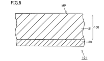
- Silicon carbide layer 100 is a silicon carbide layer epitaxially grown on single crystal layer 80.
- Single crystal layer 80 has n-type conductivity.
- Silicon carbide layer 100 has a polytype 4H hexagonal crystal structure. By adopting such a crystal structure, the on-resistance of silicon carbide semiconductor device 201 can be lowered.
- the upper surface of silicon carbide layer 100 constitutes main surface MP of silicon carbide off substrate 101.
- Silicon carbide layer 100 has an n drift layer 81, a p body layer 82, an n + layer 83, and a p contact region 84.
- N drift layer 81 has n type conductivity.
- the impurity concentration of n drift layer 81 is preferably lower than the impurity concentration of single crystal layer 80.
- the impurity concentration of the n drift layer 81 is preferably 1 ⁇ 10 15 cm ⁇ 3 or more and 5 ⁇ 10 16 cm ⁇ 3 or less.
- P body layer 82 has p type conductivity. P body layer 82 is provided on n drift layer 81.
- the impurity concentration of p body layer 82 is preferably not less than 5 ⁇ 10 15 cm ⁇ 3 and not more than 2 ⁇ 10 18 cm ⁇ 3 , and can be, for example, about 1 ⁇ 10 18 cm ⁇ 3 .
- n + layer 83 has n-type conductivity.
- N + layer 83 is provided on p body layer 82 so as to be separated from n drift layer 81 by p body layer 82. Further, a p contact region 84 is provided in the n + layer 83. N + layer 83 and p contact region 84 constitute part of main surface MP. Further, in contact with n + layer 83 and p contact region 84, source electrode 94 is provided thereon.
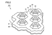
- FIG. 2 is a partial perspective view schematically showing an example of the shape of silicon carbide layer 100.
- the trench TR extends so as to form a mesh having a honeycomb structure, and an n drift layer 81 is exposed at the bottom BT of the trench TR.
- the plurality of sidewalls SW are formed so as to form a slope of a hexagonal frustum (mesa structure).
- Each sidewall SW includes a part of the n drift layer 81, the p body layer 82, the n + layer 83, and the like. Is appearing.
- the main surface MP constitutes the top surface of the mesa structure and has a hexagonal shape in plan view.
- the p contact region 84 is formed approximately at the center of the top surface, and its planar shape is similar to a hexagon (top surface).
- all the sidewalls SW are covered with the gate insulating film 91, and the gate electrode 92 is provided in the trench TR, so that the six-sided sidewall SW of the mesa structure (that is, all the sidewalls SW) can be used as the channel region. .
- the shape of silicon carbide layer 100 may be the shape shown in FIG.
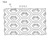
- FIG. 3 is a partial perspective view schematically showing another example of the shape of silicon carbide layer 100.
- the main surface MP extends so as to form a mesh having a honeycomb structure, and a trench TR is provided in a region surrounded by the main surface MP.
- Trench TR has a hexagonal shape in plan view. That is, the trench TR has a closed shape in a plan view by connecting a plurality of side walls SW.
- An n drift layer 81 is exposed at the bottom BT of the trench TR, and a part of the n drift layer 81, a p body layer 82, and an n + layer 83 are exposed at each side wall SW.
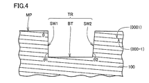
- FIG. 4 is a partially enlarged view around trench TR in silicon carbide semiconductor device 201 shown in FIG.
- the gate insulating film 91, the gate electrode 92, the n drift layer 81, and the like are not shown for easy understanding of the shape of the trench TR.
- the trench TR has a first side wall SW ⁇ b> 1 and a second side wall SW ⁇ b> 2 that face each other, and a bottom portion BT.
- the parallel oblique line group shown in FIG. 4 indicates the basal plane ((0001) plane in this example).
- main surface MP is inclined so as to have an off angle ⁇ with respect to the base surface.
- Trench TR is formed such that first side wall SW1 has an angle ⁇ 1 with respect to the base surface, and second side wall SW2 has an angle ⁇ 2 with respect to the base surface.
- the angles ⁇ 1 and ⁇ 2 are more than 65 ° and not more than 80 °.
- both the first sidewall SW1 and the second sidewall SW2 are open to the (0001) plane side (that is, the Si plane side).
- the opening directions of the first side wall SW1 and the second side wall SW2 are the same (0001) plane side, so that the surface exposed to the first side wall SW1 and the second side wall SW2 are exposed. Therefore, the channel mobility can be made substantially equal in the channel region formed along these surfaces. Therefore, during the operation of the device, current flows uniformly in each channel region, and current does not concentrate on one side. Therefore, it can have high reliability.
- the angle of the side wall SW is defined with respect to the base surface, so that the arrangement of the trench TR is not limited by the off direction of the substrate. Therefore, the degree of freedom in design is high, and it can contribute to further high integration of the silicon carbide semiconductor device.
- angles ⁇ 1 and ⁇ 2 are more preferably 70. It is more than 80 ° and less than 80 °, more preferably more than 72 ° and less than 80 °.
- FIG. 4 exemplifies a mode in which both the first side wall SW1 and the second side wall SW2 open to the (0001) plane side with the (0001) plane as the base plane.
- both the first side wall SW1 and the second side wall SW2 are open to the (000-1) plane side (that is, the C plane side).
- silicon carbide semiconductor device 201 has a plurality of sidewalls SW (a plurality of first sidewalls SW1 and second sidewalls SW2).
- the opening directions of the plurality of side walls SW are all aligned on either the Si surface side or the C surface side. Therefore, current flows evenly in all the pairs of the first side wall SW1 and the second side wall SW2 that face each other, and higher reliability can be realized.
- the difference between the angle ⁇ 1 and the angle ⁇ 2 is preferably equal to or less than the off-angle ⁇ . As described above, the difference between the angle ⁇ 1 and the angle ⁇ 2 is reduced, so that the characteristics of the channel region formed along the first sidewall SW1 and the characteristics of the channel region formed along the second sidewall SW2 are reduced. The difference with is even smaller.
- the bottom BT forms a surface extending in a direction intersecting the first side wall SW1 and the second side wall SW2, but the cross-sectional shape of the bottom BT is not limited to this, and the cross section of the trench TR The shape may be V-shaped or U-shaped.
- the hydrogen concentration in a region within 10 nm from the interface between silicon carbide off substrate 101 and gate insulating film 91 is preferably 1 ⁇ 10 18 / cm 3 or more.
- the nitrogen concentration in a region within 10 nm from the interface between silicon carbide off substrate 101 and gate insulating film 91 is preferably 1 ⁇ 10 18 / cm 3 or more.
- the hydrogen concentration and the nitrogen concentration in the region within 10 nm from the interface between the silicon carbide off substrate 101 and the gate insulating film 91 as described above should be measured by secondary ion mass spectrometry (SIMS). Can do.
- SIMS secondary ion mass spectrometry
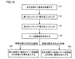
- FIG. 19 is a flowchart schematically showing a method for manufacturing the silicon carbide semiconductor device according to this embodiment.
- the method for manufacturing the silicon carbide semiconductor device according to the present embodiment includes step S1, step S2, and step S3. Further, after step S4 and step S4, step S51 and step S52 are performed. At least one of them can be provided.
- This manufacturing method can be applied to any structure shown in FIG. 2 or FIG. Hereinafter, each step will be described.
- silicon carbide off-substrate 101 having main surface MP is prepared.
- Silicon carbide off substrate 101 is prepared by forming silicon carbide layer 100 by epitaxial growth on single crystal layer 80 made of silicon carbide.
- the single crystal layer 80 can be obtained by, for example, slicing an ingot (not shown) made of polytype 4H hexagonal silicon carbide so as to have a predetermined off angle ⁇ with respect to the base surface.
- silicon carbide layer 100 is epitaxially grown on the upper surface of single crystal layer 80 having off-angle ⁇ to prepare silicon carbide off-substrate 101 having the upper surface of silicon carbide layer 100 (that is, main surface MP) having off-angle ⁇ . can do.
- Epitaxial growth of silicon carbide layer 100 is performed by, for example, CVD using a mixed gas of silane (SiH 4 ) and propane (C 3 H 8 ) as a source gas and using hydrogen gas (H 2 ) as a carrier gas, for example. (Chemical Vapor Deposition) method. At this time, it is preferable to introduce, for example, nitrogen (N) or phosphorus (P) as impurities. Thereby, n drift layer 81 is formed in silicon carbide layer 100 as shown in FIG.
- n drift layer 81 p body layer 82 and n + layer 83 are formed on n drift layer 81. These can be formed, for example, by ion implantation on the entire surface of n drift layer 81.
- an impurity for imparting p-type such as aluminum (Al)
- Al aluminum
- n + layer 83 an impurity for imparting an n-type such as phosphorus (P) is ion-implanted.
- epitaxial growth accompanied by addition of impurities may be performed.
- a resist film 60 is formed on the n + layer 83. Subsequently, as shown in FIG. 8, the resist film 60 is exposed and developed. Thereby, a mask layer 61 having an opening corresponding to a position where the p contact region 84 is to be formed is formed. Next, p contact region 84 is formed by ion implantation through mask layer 61. Thereafter, as shown in FIG. 9, the mask layer 61 is removed.
- the heat treatment temperature at this time is preferably 1500 ° C. or higher and 1900 ° C. or lower, for example, about 1700 ° C.
- the heat treatment time can be about 30 minutes, for example.
- the atmosphere of the heat treatment is preferably an inert gas atmosphere, for example, an argon (Ar) atmosphere.
- step S2 the outline of step S2 will be described with reference to FIGS.
- mask layer 40 having an opening is formed on the surface composed of n + layer 83 and p contact region 84 (on main surface MP) by photolithography.
- As mask layer 40 for example, a silicon oxide (SiO 2 ) film or the like can be used.
- the opening of mask layer 40 is formed corresponding to the position of trench TR.
- anisotropic etching is performed on main surface MP through mask layer 40, thereby forming trench TQ shown in FIG.
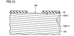
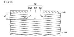
- step S2 will be described in more detail.
- 12 and 13 are partially enlarged views showing the periphery of the position where the trench TQ is formed. 12 and 13 do not show the n drift layer 81, the p body layer 82, and the like, and the dimensional relationship and the like are different from those in FIGS. 12 and 13, the hatched group in the silicon carbide off substrate 101 indicates the basal plane.
- the basal plane is described as a (0001) plane (Si plane), but the basal plane may be a (000-1) plane (C plane).
- the first etching is performed by anisotropic etching.
- anisotropic etching for example, reactive ion etching (RIE), particularly inductively coupled plasma (ICP) -RIE can be used. More specifically, for example, ICP-RIE using a mixed gas of SF 6 and O 2 as the reactive gas can be used.
- RIE reactive ion etching
- ICP inductively coupled plasma
- a trench TQ having a side wall SW substantially along the thickness direction (vertical direction in FIG. 13) of the silicon carbide off substrate 101 is formed.
- the angle ⁇ 1 formed by the first side wall SW1 and the (0001) plane is 0 ° or more and less than 90 °. That is, the opening direction of the first sidewall SW1 is the Si surface side.
- the angle ⁇ 2 formed by the second side wall SW2 and the (0001) plane exceeds 90 °. Therefore, the opening direction of the second side wall SW2 is the opposite side of the (0001) plane, that is, the C plane side.
- step S2 etching is preferably performed so that an angle ⁇ 1 formed between first sidewall SW1 and basal plane of trench TQ is 80 ° or more. This is because it becomes easier to expose substantially equivalent surfaces to the first sidewall SW1 and the second sidewall SW2 in step S3 described later.
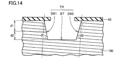
- FIG. 14 illustrates an embodiment in which the opening directions of the first sidewall SW1 and the second sidewall SW2 are aligned on the Si surface side, but the opening directions may be aligned on the C surface side.
- thermal etching performed in an atmosphere containing a reactive gas having at least one kind of halogen atom is suitable.
- the at least one or more halogen atoms include at least one of chlorine (Cl) atoms and fluorine (F) atoms.
- Cl 2 , BCl 3 , SF 6 , or CF 4 can be used as the reaction gas.
- specific thermal etching conditions a mixed gas of chlorine gas and oxygen gas is used as a reaction gas, and the heat treatment temperature can be set to 700 ° C. or higher and 1000 ° C. or lower, for example.
- the flow rate ratio of chlorine gas to oxygen gas is preferably 0.5 or more and 4.0 or less, more preferably 1.0 or more and 2.0 or less. It is.
- the reaction gas may contain a carrier gas in addition to the above-described chlorine gas and oxygen gas.
- the carrier gas for example, nitrogen (N 2 ) gas, argon gas, helium gas or the like can be used.
- the heat treatment temperature is set to 700 ° C. or higher and 1000 ° C. or lower as described above, the etching rate of silicon carbide (SiC) is about 70 ⁇ m / hr, for example.
- the selectivity ratio of SiC to SiO 2 can be made extremely large, so that the mask layer 40 made of SiO 2 is substantially not etched during SiC etching. Not etched.
- the angle ⁇ 1 and the angle ⁇ 2 can be more than 65 ° and 80 ° or less by appropriately adjusting the time required for the etching. At this time, the angle ⁇ 1 and the angle ⁇ 2 are preferably more than 70 ° and 80 ° or less, more preferably more than 72 ° and 80 ° or less.
- the removal depth (d1 in FIGS. 13 and 14) by the first etching is the second etching ( It is preferably deeper than the removal depth (d2 in FIG. 14) by isotropic etching.
- the opening direction of side walls SW facing each other is aligned with main surface MP of silicon carbide off-substrate 101, and the surface is substantially equivalent to side walls SW facing each other.
- the mask layer 40 can be removed by an arbitrary method such as etching as shown in FIG.
- step S4 for forming gate insulating film 91 covering sidewall SW and bottom portion BT of trench TR can be performed.
- the gate insulating film 91 can be formed by thermal oxidation, for example.
- the opening direction of the sidewall SW (the first sidewall SW1 and the second SW2) may be either the Si surface side or the C surface side.
- the step S51 of introducing hydrogen into the interface between the silicon carbide off substrate 101 and the gate insulating film 91 is performed. It is preferable.
- heat treatment using hydrogen (H 2 ) gas as the atmospheric gas is preferably performed.
- hydrogen annealing for example, conditions in which the heat treatment temperature is 1100 ° C. to 1300 ° C. and the heat treatment time is about 1 hour can be used.
- hydrogen can be introduced into the interface between silicon carbide off substrate 101 and gate insulating film 91.
- the formation of interface states is suppressed at the interface between the sidewall SW having characteristics approximate to the C-plane and the gate insulating film 91, and channel mobility is improved in the semiconductor device.
- water vapor or water vapor-containing oxygen gas can be used as the atmospheric gas instead of hydrogen gas.
- Step S52 When the opening direction of sidewall SW is the C-plane side, step S52 for introducing nitrogen into the interface between silicon carbide off substrate 101 and gate insulating film 91 is performed after gate insulating film 91 is formed. Is preferred.
- nitrogen annealing heat treatment using nitrogen monoxide (NO) gas as the atmospheric gas (hereinafter also referred to as “nitrogen annealing”) is preferably performed.
- a heat treatment condition for nitrogen annealing for example, a heat treatment temperature of 1100 ° C. to 1300 ° C. and a heat treatment time of about 1 hour can be used.
- nitrogen can be introduced into the interface between silicon carbide off substrate 101 and gate insulating film 91.
- a mixed gas of N 2 and O 2 , N 2 O gas, or the like can be used as the atmospheric gas instead of NO gas.
- heat treatment using an inert gas may be performed after the above-described hydrogen annealing or nitrogen annealing.
- heat treatment (hereinafter also referred to as “Ar annealing”) may be performed in an Ar gas atmosphere.
- the heat treatment temperature for Ar annealing is preferably higher than the heat treatment temperature for hydrogen annealing or nitrogen annealing and lower than the melting point of the gate insulating film 91.
- the heat treatment time is, for example, about 1 hour.
- a gate electrode 92 is formed on the gate insulating film 91 as shown in FIG. Specifically, gate electrode 92 is formed on gate insulating film 91 so as to fill the region inside trench TR with gate insulating film 91 interposed therebetween.
- the gate electrode 92 can be formed by, for example, film formation of a conductor or polydoped silicon and CMP (Chemical Mechanical Polishing).
- interlayer insulating film 93 is formed on gate electrode 92 and gate insulating film 91 so as to cover the exposed surface of gate electrode 92. Subsequently, etching is performed so that openings are formed in the interlayer insulating film 93 and the gate insulating film 91. Through this opening, n + layer 83 and p contact region 84 are exposed. Then, source electrode 94 is formed in contact with each of exposed n + layer 83 and p contact region 84. Further, in single crystal layer 80, drain electrode 98 is formed on the back surface opposite to the main surface on which n drift layer 81 is formed.
- source wiring layer 95 is formed on source electrode 94.
- substantially equivalent surfaces appear on first sidewall SW1 and second sidewall SW2 facing each other in trench TR, and a silicon carbide semiconductor device with high reliability is manufactured.
- the arrangement of trench TR does not depend on the off direction of silicon carbide off substrate 101. Therefore, the degree of freedom in design is high, and the silicon carbide semiconductor device can be highly integrated.
Landscapes
- Engineering & Computer Science (AREA)
- Power Engineering (AREA)
- Microelectronics & Electronic Packaging (AREA)
- Physics & Mathematics (AREA)
- Condensed Matter Physics & Semiconductors (AREA)
- General Physics & Mathematics (AREA)
- Computer Hardware Design (AREA)
- Ceramic Engineering (AREA)
- Crystallography & Structural Chemistry (AREA)
- Chemical & Material Sciences (AREA)
- Manufacturing & Machinery (AREA)
- Electrodes Of Semiconductors (AREA)
- Recrystallisation Techniques (AREA)
Abstract
炭化珪素半導体装置は、基底面に対するオフ角度(θ)を有する主表面(MP)を含む炭化珪素オフ基板(101)を備え、主表面(MP)には、トレンチ(TR)が設けられ、トレンチ(TR)は、複数の側壁(SW)と底部(BT)とを有し、さらに、側壁(SW)と底部(BT)とを覆うゲート絶縁膜(91)と、ゲート絶縁膜(91)上に設けられたゲート電極(92)と、を備え、トレンチ(TR)における側壁(SW)の基底面に対する角度が、65°を超え80°以下であり、複数の側壁(SW)の開口方向が、シリコン面側またはカーボン面側のいずれかに揃っている。
Description
本発明は、炭化珪素半導体装置に関する。
炭化珪素半導体装置は、現在主流である珪素半導体装置に比べて、電力損失が少なく、高温動作が可能である等の多くの利点を有しており、次世代の電力用半導体装置として期待されている。従来、半導体装置の構造として様々な構造が提案されている。たとえばトレンチゲート構造では、半導体基板にトレンチと呼ばれる溝が設けられる(たとえば、特開2012-146921号公報(特許文献1)参照。)。
トレンチゲート構造では、トレンチの側壁に沿ってチャネル領域が形成される。すなわち、半導体装置の縦方向(基板の表面に対して垂直方向)にチャネル領域が形成される。このため半導体装置の微細化および高集積化が可能である。
ところで、炭化珪素半導体基板は、エピタキシャル成長を行なうために、主表面が基底面(たとえば(0001)面)に対して所定のオフ角度を有するのが一般的である。このため炭化珪素半導体基板の表面にトレンチを設けると、通常は、トレンチ内において互いに対向する二つの側壁はそれぞれ面方位が異なることになる。
このように互いに対向する側壁の面方位が異なると、それぞれの側壁に沿って形成されるチャネル領域においても、電気特性(チャネル移動度)が異なることとなる。これにより互いに対向する側壁で、電流のアンバランスが生じ、長期使用において炭化珪素半導体装置の信頼性が低下する場合がある。これは、抵抗の低い部分を優先して電流が流れるため、一方の側壁に沿って形成されたチャネル領域に電流が集中してしまうからである。
このような問題に対応するため、特許文献1では、トレンチを延設する方向を、基板のオフ方向に対して、所定の角度を有するように規定することにより、対向する側壁の面方位が異なることを抑制している。
しかしながら、炭化珪素半導体装置には、更なる高集積化が求められている。特許文献1の方法によれば、基板のオフ方向に対して、トレンチの配置が一義的に決定されるため、設計上の自由度が小さくなり、炭化珪素半導体装置の高集積化に関して制約となる場合がある。
そこで上記課題に鑑みて、高集積化が可能であるとともに、信頼性が高い炭化珪素半導体装置を提供することを目的とする。
本発明の一態様に係る炭化珪素半導体装置は、基底面に対するオフ角度を有する主表面を含む炭化珪素オフ基板を備える。ここで、主表面には、トレンチが設けられ、当該トレンチは、複数の側壁と底部とを有している。さらに、炭化珪素半導体装置は、該側壁と該底部とを覆うゲート絶縁膜と、ゲート絶縁膜上に設けられたゲート電極と、を備えるものである。
そして、トレンチにおける側壁の基底面に対する角度が、65°を超え80°以下であり、複数の側壁の開口方向が、シリコン面側またはカーボン面側のいずれかに揃っている。
上記の炭化珪素半導体装置は、高集積化が可能であるとともに、信頼性が高い。
以下、本発明に係わる一実施形態についてさらに詳細に説明する。なお、以下の図面において同一または相当する部分には同一の参照符号を付し、その説明は繰り返さない。また、本明細書中の結晶学的な記載においては、個別方位を[]、集合方位を<>、個別面を()、集合面{}で、それぞれ示すものとする。また、結晶学上の指数が負であることは、通常、”-”(バー)を数字の上に付すことによって表現されるが、本明細書中では数字の前に負の符号を付すことで表現するものとする。
[本願発明の実施形態の説明]
まず、本発明の一実施形態(以下、「本実施形態」とも記す)の概要を以下の(1)~(14)に列記して説明する。
まず、本発明の一実施形態(以下、「本実施形態」とも記す)の概要を以下の(1)~(14)に列記して説明する。
本発明者は、上記課題を解決するため鋭意研究を行なったところ、基底面に対して、トレンチの側壁が特定の角度を有するように、トレンチを形成することにより、互いに対向する側壁に形成されるチャネル領域の特性をほぼ等価なものとすることができるとの知見を得、該知見に基づきさらに研究を重ねることにより、本実施形態を完成させるに至った。すなわち、本実施形態に係る炭化珪素半導体装置は以下の構成を備える。
(1)本実施形態に係る炭化珪素半導体装置201は、基底面に対するオフ角度θを有する主表面MPを含む炭化珪素オフ基板101を備える。ここで主表面MPにはトレンチTRが設けられ、トレンチTRは複数の側壁SWと底部BTとを有している。さらに炭化珪素半導体装置201は、側壁SWと底部BTとを覆うゲート絶縁膜91と、ゲート絶縁膜91上に設けられたゲート電極92と、を備える。
そして、トレンチTRにおける側壁SWの基底面に対する角度θ1,θ2が、65°を超え80°以下であり、複数の側壁SWの開口方向が、シリコン面側またはカーボン面側のいずれかに揃っている。
なおここで、基底面とは(0001)面または(000-1)面を示す。また、「シリコン面」とは(0001)面を示し、「カーボン面」とは(000-1)面を示し、以下の説明においては、「シリコン面」を「Si面」、「カーボン面」を「C面」と記すことがある。
さらに、図4を参照して、「側壁SWの開口方向がシリコン面側である」とは、側壁SWと(0001)面とのなす角度θ1およびθ2が、0°以上90°未満であることを示し、「側壁SWの開口方向がカーボン面側である」とは、側壁SWと(000-1)面とのなす角度θ1およびθ2が0°以上90°未満であることを示す。
以上の構成を備える炭化珪素半導体装置201によれば、トレンチTRの互いに対向する側壁SWにほぼ等価な結晶面を表出させることができる。すなわち、互いに対向する側壁SWに沿って形成されるチャネル領域の特性(チャネル移動度)をほぼ同等なものとすることができる。これにより、対向する側壁SWに形成されたチャネル領域同士で電流のアンバランスが生じることを防止できるため、高い信頼性を有することができる。また、炭化珪素オフ基板101のオフ方向に対して、トレンチTRの配置が制限されないため、炭化珪素半導体装置の更なる高集積化が可能である。
(2)炭化珪素オフ基板101は、オフ方向が<11-20>方向であることが好ましい。オフ方向が<11-20>方向である炭化珪素オフ基板は市場における入手の容易性が高く好適である。
(3)炭化珪素オフ基板101のオフ角度θは、1°以上8°以下であることが好ましい。これにより、炭化珪素オフ基板101は、結晶欠陥の少ない基板となることができる。
(4)トレンチTRは、複数の側壁SWが連なることにより、平面視において閉じた形状を有しており、すべての側壁SWがゲート絶縁膜91に覆われていることが好ましい。これにより、すべての側壁SWに沿ってチャネル領域が形成され、かつそれぞれの側壁SWでのチャネル移動度がほぼ等価であるため、さらに信頼性の向上した炭化珪素半導体装置を構成することができる。
(5)複数の側壁SWは互いに対向する第1の側壁SW1および第2の側壁SW2を含み、第1の側壁SW1の基底面に対する角度θ1と、第2の側壁SW2の基底面に対する角度θ2との差異は、オフ角度θ以下であることが好ましい。これにより、第1の側壁SW1に沿って形成されるチャネル領域の特性と、第2の側壁SW2に沿って形成されるチャネル領域の特性とを、より一層近似させることができる。
(6)複数の側壁SWの開口方向が、すべてシリコン面側であることが好ましい。これにより、すべての側壁SWに表出する面をカーボン面に近似した結晶面とすることができるため、すべてのチャネル領域でカーボン面に近似した特性を利用することができる。
(7)炭化珪素オフ基板101とゲート絶縁膜91との界面から10nm以内の領域における水素濃度が、1×10¹⁸/cm3以上であることが好ましい。これにより、シリコン面側に開口した側壁SWとゲート絶縁膜91との界面において、界面準位の形成が抑制され、チャネル移動度を向上させることができる。
(8)複数の側壁SWの開口方向が、すべてカーボン面側であることが好ましい。これにより、すべての側壁SWに表出する面をシリコン面に近似した結晶面とすることができるため、すべてのチャネル領域でシリコン面に近似した特性を利用することができる。
(9)炭化珪素オフ基板101とゲート絶縁膜91との界面から10nm以内の領域における窒素濃度が、1×10¹⁸/cm3以上であることが好ましい。これにより、カーボン面側に開口した側壁SWとゲート絶縁膜91との界面において、界面準位の形成が抑制され、チャネル移動度を向上させることができる。
(10)上記の炭化珪素半導体装置は、次の製造方法によって製造することができる。すなわち、炭化珪素半導体装置の製造方法は、主表面MPを有する炭化珪素オフ基板101を準備する工程S1と、主表面MPに対して、異方性のエッチングを行なうことにより、側壁SWと底部BTとを有するトレンチTQを形成する第1のエッチング工程S2と、側壁SWおよび底部BTに対して、等方性のエッチングを行なうことにより、側壁SWの基底面に対する角度θ1,θ2を65°を超え80°以下とする第2のエッチング工程S3と、を備える。
これにより、トレンチTRの互いに対向する側壁SWの開口方向をシリコン面側またはカーボン面側のいずれかに揃えることができ、対向する側壁SWにほぼ等価な結晶面が表出した炭化珪素半導体装置を製造することができる。
(11)第1のエッチング工程S2により除去される炭化珪素オフ基板101の除去深さd1が、第2のエッチング工程S3により除去される炭化珪素オフ基板101の除去深さd2よりも深いことが好ましい。これにより、さらに確実に互いに対向する側壁SWにほぼ等価な結晶面を表出させることができる。
(12)第1のエッチング工程S2は、側壁SWの基底面に対する角度が80°以上となるように、主表面MPをエッチングする工程を含むことが好ましい。これにより、第2のエッチング工程S3でのエッチングにより側壁SWが部分的に除去されたとき、当該エッチング後の側壁SWの基底面に対する角度を容易に80°以下とすることができる。このため、さらに確実に互いに対向する側壁SWにほぼ等価な結晶面を表出させることができる。
(13)側壁SWの開口方向が、シリコン面側である場合、炭化珪素半導体装置の製造方法は、側壁SWと底部BTとを覆うゲート絶縁膜91を形成する工程S4と、炭化珪素オフ基板101とゲート絶縁膜91との界面に水素を導入する工程S51と、をさらに備えることが好ましい。これにより、当該界面での界面準位の形成が抑制され、チャネル移動度が向上した炭化珪素半導体装置を製造することができる。
(14)側壁SWの開口方向が、カーボン面側である場合、炭化珪素半導体装置の製造方法は、側壁SWと底部BTとを覆うゲート絶縁膜91を形成する工程S4と、炭化珪素オフ基板101とゲート絶縁膜91との界面に窒素を導入する工程S52と、をさらに備えることが好ましい。これにより、当該界面での界面準位の形成が抑制され、チャネル移動度が向上した炭化珪素半導体装置を製造することができる。
[本願発明の実施形態の詳細]
以下、本実施形態に係る炭化珪素半導体装置について、より詳細に説明するが、本実施形態はこれらに限定されるものではない。
以下、本実施形態に係る炭化珪素半導体装置について、より詳細に説明するが、本実施形態はこれらに限定されるものではない。
<炭化珪素半導体装置>
図1は、本実施形態に係る炭化珪素半導体装置201の構成を概略的に示す断面図である。図1に示す炭化珪素半導体装置201は、トレンチゲート型MOSFET(Metal Oxide Semiconductor Field Effect Transistor)として構成されている。炭化珪素半導体装置201は、炭化珪素オフ基板101と、ゲート絶縁膜91と、ゲート電極92と、層間絶縁膜93と、ソース電極94と、ソース配線層95と、ドレイン電極98とを有する。炭化珪素オフ基板101は、単結晶層80と、単結晶層80上にエピタキシャル成長させられた炭化珪素層100とからなる。炭化珪素オフ基板101の主表面MPには、側壁SWと底部BTとを有するトレンチTRが設けられている。そして、炭化珪素半導体装置201では、側壁SWに沿ってチャネル領域が形成される。
図1は、本実施形態に係る炭化珪素半導体装置201の構成を概略的に示す断面図である。図1に示す炭化珪素半導体装置201は、トレンチゲート型MOSFET(Metal Oxide Semiconductor Field Effect Transistor)として構成されている。炭化珪素半導体装置201は、炭化珪素オフ基板101と、ゲート絶縁膜91と、ゲート電極92と、層間絶縁膜93と、ソース電極94と、ソース配線層95と、ドレイン電極98とを有する。炭化珪素オフ基板101は、単結晶層80と、単結晶層80上にエピタキシャル成長させられた炭化珪素層100とからなる。炭化珪素オフ基板101の主表面MPには、側壁SWと底部BTとを有するトレンチTRが設けられている。そして、炭化珪素半導体装置201では、側壁SWに沿ってチャネル領域が形成される。
なお、以下の説明において、複数の側壁を総称して側壁SWと記すことがあり、また個別の側壁を、第1の側壁SW1または第2の側壁SW2と記すことがある。また、以下の説明における各層または領域等の導電型はあくまでも例示であり、各層または領域等の極性は、これらに限定されるものではない。
炭化珪素オフ基板101の主表面MPは、基底面(すなわち(0001)面または(000-1)面)に対して、オフ角度θ(図4参照)を有するように傾いている。オフ角度θは、1°以上8°以下であることが好ましい。これにより、エピタキシャル成長によって形成される炭化珪素層100の結晶品質が高まるからである。なお、オフ角度θは、より好ましくは2°以上6°以下であり、さらに好ましくは3°以上5°以下である。また、炭化珪素オフ基板101のオフ方向は、<11-20>方向であることが好ましい。オフ方向が<11-20>方向である炭化珪素オフ基板は市場における入手の容易性が高いからである。
炭化珪素層100は、単結晶層80上にエピタキシャル成長させられた炭化珪素層である。単結晶層80は、n型の導電型を有する。炭化珪素層100は、ポリタイプ4Hの六方晶の結晶構造を有する。かかる結晶構造を採用することにより、炭化珪素半導体装置201のオン抵抗を低くすることができる。炭化珪素層100の上面は、炭化珪素オフ基板101の主表面MPを構成している。炭化珪素層100は、nドリフト層81と、pボディ層82と、n+層83と、pコンタクト領域84とを有する。
nドリフト層81は、n型の導電型を有する。nドリフト層81の不純物濃度は、単結晶層80の不純物濃度よりも低いことが好ましい。ここで、nドリフト層81の不純物濃度は、好ましくは1×1015cm-3以上5×1016cm-3以下である。
pボディ層82は、p型の導電型を有する。pボディ層82はnドリフト層81上に設けられている。pボディ層82の不純物濃度は、5×1015cm-3以上2×1018cm-3以下であることが好ましく、たとえば、1×1018cm-3程度とすることができる。
n+層83は、n型の導電型を有する。n+層83は、pボディ層82によってnドリフト層81から隔てられるように、pボディ層82上に設けられている。さらに、n+層83内にはpコンタクト領域84が設けられている。n+層83およびpコンタクト領域84は、主表面MPの一部を構成している。さらに、n+層83およびpコンタクト領域84に接して、この上にソース電極94が設けられている。
炭化珪素層100の上面、すなわち炭化珪素オフ基板101の主表面MPにはトレンチTRが設けられている。ここで、トレンチTRを有する炭化珪素層100の形状について説明する。図2は、炭化珪素層100の形状の一例を概略的に示す部分斜視図である。この例において、トレンチTRはハニカム構造の網目を構成するように伸びており、トレンチTRの底部BTには、nドリフト層81が表出している。そして、複数の側壁SWは、六角錐台(メサ構造)の斜面をなすように形成されており、それぞれの側壁SWには、nドリフト層81の一部とpボディ層82とn+層83とが表出している。主表面MPは、メサ構造の頂面を構成しており、平面視では六角形状を有している。pコンタクト領域84は、メサ構造において、頂面のほぼ中央に形成され、その平面形状は六角形(頂面)と相似形である。そして、すべての側壁SWがゲート絶縁膜91に覆われ、トレンチTR内にゲート電極92が設けられることにより、メサ構造の六面の側壁SW(すなわち、すべての側壁SW)がチャネル領域として利用できる。
また、炭化珪素層100の形状は、図3に示す形状であってもよい。図3は、炭化珪素層100の形状の他の一例を概略的に示す部分斜視図である。この例においては、主表面MPがハニカム構造の網目を構成するように伸びており、主表面MPによって取り囲まれた領域内にトレンチTRが設けられている。トレンチTRは、平面視では六角形状を有している。すなわち、トレンチTRは複数の側壁SWが連なることにより、平面視において閉じた形状を有している。そして、トレンチTRの底部BTにはnドリフト層81が表出しており、それぞれの側壁SWにはnドリフト層81の一部とpボディ層82とn+層83とが表出している。この構造において、すべての側壁SWがゲート絶縁膜91に覆われ、トレンチTR内にゲート電極92が設けられることにより、トレンチTR内の六面の側壁SW(すなわち、すべての側壁SW)がチャネル領域として利用できる。
次に、トレンチTRの詳細な形状について説明する。図4は、図1に示す炭化珪素半導体装置201におけるトレンチTR周辺の部分拡大図である。なお図4には、トレンチTRの形状を分かりやすく図示するため、ゲート絶縁膜91、ゲート電極92、およびnドリフト層81等を図示していない。
図4に示すように、トレンチTRは、互いに対向する第1の側壁SW1および第2の側壁SW2と底部BTとを有している。ここで、図4に示す平行な斜線群は、基底面(この例では(0001)面)を示している。図4に示すように、主表面MPは基底面に対してオフ角度θを有するように傾いている。そして、トレンチTRは、第1の側壁SW1が基底面に対する角度θ1を有し、第2の側壁SW2が基底面に対する角度θ2を有するように形成されている。本実施形態では、角度θ1およびθ2は、65°を超え80°以下である。そして図4では、第1の側壁SW1および第2の側壁SW2は、ともに(0001)面側(すなわち、Si面側)に開口している。
これにより、第1の側壁SW1および第2の側壁SW2のそれぞれの開口方向が同じ(0001)面側になるので、第1の側壁SW1に表出する面と、第2の側壁SW2に表出する面とが互いにほぼ等価な面となり、これらに沿って形成されるチャネル領域においてチャネル移動度をほぼ同等にすることができる。したがって装置の動作時には、それぞれのチャネル領域に均等に電流が流れ、一方に電流が集中することがない。そのため高い信頼性を有することができる。
また本実施形態においては、基底面に対して側壁SWの角度を規定するため、基板のオフ方向によってトレンチTRの配置が制限されることがない。したがって、設計上の自由度が高く、炭化珪素半導体装置の更なる高集積化に資することができる。
なおここで、第1の側壁SW1に表出する面と、第2の側壁SW2に表出する面とを、より等価な面に近づけるとの観点から、角度θ1およびθ2は、より好ましくは70°を超え80°以下であり、さらに好ましくは72°を超え80°以下である。
また図4は、基底面を(0001)面として、第1の側壁SW1および第2の側壁SW2が、ともに(0001)面側に開口する態様を例示したが、基底面は(000-1)面であってもよく、その場合は第1の側壁SW1および第2の側壁SW2は、ともに(000-1)面側(すなわち、C面側)に開口することとなる。
さらに、前述の図2または図3に示されるように、炭化珪素半導体装置201は、複数の側壁SW(複数の第1の側壁SW1および第2の側壁SW2)を有している。本実施形態では、複数の側壁SWの開口方向が、すべてSi面側またはC面側のいずれかに揃っている。したがって、すべての互いに対向する第1の側壁SW1および第2の側壁SW2の組において、均等に電流が流れることとなり、より一層高い信頼性を実現することができる。
ここで、角度θ1と角度θ2との差異は、オフ角度θ以下であることが好ましい。このように、角度θ1と角度θ2との差異が小さくなることにより、第1の側壁SW1に沿って形成されるチャネル領域の特性と、第2の側壁SW2に沿って形成されるチャネル領域の特性との差異もより一層小さくなる。
なお図1等において、底部BTは第1の側壁SW1および第2の側壁SW2と交差する方向に伸びる面を構成しているが、底部BTの断面形状はこれに限定されず、トレンチTRの断面形状はV字形状やU字形状等であってもよい。
本実施形態において、複数の側壁SWの開口方向が、すべてSi面側である場合、すべてのチャネル領域でC面に近似した特性を利用することができる。すべての側壁SWに表出する面がC面に近似した結晶面となるからである。そして、この場合、炭化珪素オフ基板101とゲート絶縁膜91との界面から10nm以内の領域における水素濃度は、1×10¹⁸/cm3以上であることが好ましい。C面に近似した特性を有する側壁SWとゲート絶縁膜91との界面に水素(H)が導入されることによって、界面準位の形成が効率的に抑制され、チャネル移動度を向上させることができるからである。なお、水素濃度は、より好ましくは1×1021/cm3以上である。
また、本実施形態において、複数の側壁SWの開口方向が、すべてC面側である場合、すべてのチャネル領域でSi面に近似した特性を利用することができる。すべての側壁SWに表出する面がSi面に近似した結晶面となるからである。そしてこの場合、炭化珪素オフ基板101とゲート絶縁膜91との界面から10nm以内の領域における窒素濃度は、1×10¹⁸/cm3以上であることが好ましい。Si面に近似した特性を有する側壁SWとゲート絶縁膜91との界面に窒素(N)が導入されることによって、界面準位の形成が効率的に抑制され、チャネル移動度を向上させることができるからである。なお窒素濃度は、より好ましくは1×1021/cm3以上である。
なお、上記のような炭化珪素オフ基板101とゲート絶縁膜91との界面から10nm以内の領域における水素濃度および窒素濃度は、二次イオン質量分析法(SIMS:Secondary Ion Mass Spectrometry)によって計測することができる。
<炭化珪素半導体装置の製造方法>
以上に説明した本実施形態の炭化珪素半導体装置は、次のような製造方法によって製造することができる。図19は、本実施形態に係る炭化珪素半導体装置の製造方法の概略を示すフローチャートである。図19に示すように、本実施形態に係る炭化珪素半導体装置の製造方法は、工程S1、工程S2および工程S3を備えるものであり、さらに工程S4と、工程S4の後に工程S51および工程S52の少なくともいずれかを備えることができる。なおこの製造方法は、図2または図3に示すいずれの構造に対しても適用可能である。以下、各工程について説明する。
以上に説明した本実施形態の炭化珪素半導体装置は、次のような製造方法によって製造することができる。図19は、本実施形態に係る炭化珪素半導体装置の製造方法の概略を示すフローチャートである。図19に示すように、本実施形態に係る炭化珪素半導体装置の製造方法は、工程S1、工程S2および工程S3を備えるものであり、さらに工程S4と、工程S4の後に工程S51および工程S52の少なくともいずれかを備えることができる。なおこの製造方法は、図2または図3に示すいずれの構造に対しても適用可能である。以下、各工程について説明する。
<工程S1>
工程S1では、主表面MPを有する炭化珪素オフ基板101を準備する。炭化珪素オフ基板101は、炭化珪素からなる単結晶層80上にエピタキシャル成長によって炭化珪素層100を形成することにより準備される。ここで単結晶層80は、たとえば、ポリタイプ4Hの六方晶炭化珪素からなるインゴット(図示せず)を、基底面に対して所定のオフ角度θを有するようにスライスすることによって得ることができる。そしてオフ角度θを有する単結晶層80の上面において炭化珪素層100をエピタキシャル成長させることにより、炭化珪素層100の上面(すなわち、主表面MP)が、オフ角度θを有する炭化珪素オフ基板101を準備することができる。
工程S1では、主表面MPを有する炭化珪素オフ基板101を準備する。炭化珪素オフ基板101は、炭化珪素からなる単結晶層80上にエピタキシャル成長によって炭化珪素層100を形成することにより準備される。ここで単結晶層80は、たとえば、ポリタイプ4Hの六方晶炭化珪素からなるインゴット(図示せず)を、基底面に対して所定のオフ角度θを有するようにスライスすることによって得ることができる。そしてオフ角度θを有する単結晶層80の上面において炭化珪素層100をエピタキシャル成長させることにより、炭化珪素層100の上面(すなわち、主表面MP)が、オフ角度θを有する炭化珪素オフ基板101を準備することができる。
炭化珪素層100のエピタキシャル成長は、たとえば、原料ガスとして、シラン(SiH4)とプロパン(C3H8)との混合ガスを用い、キャリアガスとして、たとえば水素ガス(H2)を用いたCVD(Chemical Vapor Deposition)法により行なうことができる。この際、不純物として、たとえば窒素(N)やリン(P)を導入することが好ましい。これにより図5に示すように、炭化珪素層100内にnドリフト層81が形成される。
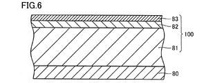
次に図6に示すように、nドリフト層81上に、pボディ層82およびn+層83が形成される。これらの形成は、たとえばnドリフト層81の全面上へのイオン注入によって行なうことができる。pボディ層82を形成するためのイオン注入では、たとえばアルミニウム(Al)等のp型を付与するための不純物がイオン注入される。またn+層83を形成するためのイオン注入では、たとえばリン(P)等のn型を付与するための不純物がイオン注入される。なおイオン注入の代わりに、不純物の添加を伴うエピタキシャル成長を行なってもよい。
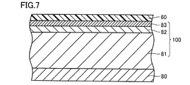
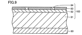
次に図7に示すように、n+層83上にレジスト膜60が形成される。続いて図8に示すように、レジスト膜60に対して露光および現像が行なわれる。これにより、pコンタクト領域84が形成されることとなる位置に対応した開口を有するマスク層61が形成される。次にマスク層61を介してイオン注入を行なうことにより、pコンタクト領域84が形成される。その後、図9に示すようにマスク層61は除去される。
次に、不純物を活性化するための熱処理が行なわれる。このときの熱処理温度は、好ましくは1500℃以上1900℃以下であり、たとえば1700℃程度である。熱処理時間は、たとえば30分程度とすることができる。熱処理の雰囲気は、好ましくは不活性ガス雰囲気であり、たとえばアルゴン(Ar)雰囲気である。
<工程S2>
次に、図10および11、ならびに図12および13を参照して、主表面MPに対して、異方性のエッチングを行なうことにより、側壁SWと底部BTとを有するトレンチTQを形成する第1のエッチング工程S2が実行される。
次に、図10および11、ならびに図12および13を参照して、主表面MPに対して、異方性のエッチングを行なうことにより、側壁SWと底部BTとを有するトレンチTQを形成する第1のエッチング工程S2が実行される。
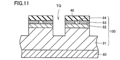
まず、図10および11を参照して、工程S2の概略を説明する。図10に示すように、n+層83およびpコンタクト領域84からなる面上(主表面MP上)に、開口部を有するマスク層40がフォトリソグラフィ法によって形成される。マスク層40としては、たとえば酸化珪素(SiO2)膜等を用いることができる。またマスク層40の開口部は、トレンチTRの位置に対応して形成される。次にマスク層40を介して、主表面MPに対して異方性のエッチングを行なうことにより、図11に示すトレンチTQが形成される。
さらに、図12および13を参照して、工程S2をより詳細に説明する。図12および13は、トレンチTQが形成される位置の周辺を示す部分拡大図である。図12および13には、説明を分かりやすくするため、nドリフト層81やpボディ層82等を図示せず、さらに寸法関係等も図10および11とは異ならせている。また、図12および13において、炭化珪素オフ基板101内の斜線群は基底面を示している。また、以下の説明において、基底面を(0001)面(Si面)として説明するが、基底面は(000-1)面(C面)であってもよい。
図12および13を参照して、第1のエッチングは、異方性のエッチングによって行なわれる。異方性のエッチングとしては、たとえば、反応性イオンエッチング(RIE)、特に誘導結合プラズマ(ICP)-RIEを用いることができる。より具体的には、たとえば反応性ガスとしてSF6とO2との混合ガスを用いたICP-RIEを用いることができる。
このような異方性のエッチングにより、炭化珪素オフ基板101の厚さ方向(図13中の縦方向)に、ほぼ沿った側壁SWを有するトレンチTQが形成される。このとき、図13に示すように、第1の側壁SW1と(0001)面とのなす角度θ1は0°以上90°未満となっている。すなわち、第1の側壁SW1の開口方向はSi面側である。これに対して、第2の側壁SW2と(0001)面とのなす角度θ2は90°を超えている。したがって第2の側壁SW2の開口方向は、(0001)面の反対側、すなわちC面側である。つまりこの状態では、第1の側壁SW1と第2の側壁SW2は、互いに開口方向が異なっている。なお工程S2においては、トレンチTQの第1の側壁SW1と基底面とのなす角度θ1が、80°以上となるように、エッチングが行なわれることが好ましい。これにより、後述する工程S3において、第1の側壁SW1および第2の側壁SW2にほぼ等価な面を表出させやすくなるからである。
<工程S3>
次に、図14に示すように、工程S2によって形成された第1の側壁SW1、第2の側壁SW2、および底部BTに対して等方性のエッチングを行なうことにより、第1の側壁SW1および第2の側壁SW2の基底面に対する角度を65°を超え80°以下とする第2のエッチング工程S3が実行される。これにより、第1の側壁SW1の開口方向と、第2の側壁SW2の開口方向が揃うとともに、第1の側壁SW1に表出する面と、第2の側壁SW2に表出する面とをほぼ等価な面とすることができる。なお図14では、第1の側壁SW1および第2の側壁SW2の開口方向がSi面側に揃っている態様を例示しているが、その開口方向はC面側に揃っていてもよい。
次に、図14に示すように、工程S2によって形成された第1の側壁SW1、第2の側壁SW2、および底部BTに対して等方性のエッチングを行なうことにより、第1の側壁SW1および第2の側壁SW2の基底面に対する角度を65°を超え80°以下とする第2のエッチング工程S3が実行される。これにより、第1の側壁SW1の開口方向と、第2の側壁SW2の開口方向が揃うとともに、第1の側壁SW1に表出する面と、第2の側壁SW2に表出する面とをほぼ等価な面とすることができる。なお図14では、第1の側壁SW1および第2の側壁SW2の開口方向がSi面側に揃っている態様を例示しているが、その開口方向はC面側に揃っていてもよい。
等方性のエッチングとしては、少なくとも1種以上のハロゲン原子を有する反応性ガスを含む雰囲気中で行なわれる熱エッチングが好適である。この熱エッチングにおいて、少なくとも1種以上のハロゲン原子には、塩素(Cl)原子およびフッ素(F)原子の少なくともいずれかが含まれる。たとえば、反応ガスとしてCl2、BCl3、SF6、またはCF4を用いることができる。具体的な熱エッチングの条件は、塩素ガスと酸素ガスとの混合ガスを反応ガスとして用い、熱処理温度は、たとえば700℃以上1000℃以下とすることができる。
ここで、酸素ガスに対する塩素ガスの流量比率((塩素ガス流量)/(酸素ガス流量))は、好ましくは0.5以上4.0以下であり、より好ましくは1.0以上2.0以下である。また、反応ガスは、上述した塩素ガスと酸素ガスとに加えて、キャリアガスを含んでいてもよい。キャリアガスとしては、たとえば窒素(N2)ガス、アルゴンガス、ヘリウムガスなどを用いることができる。そして、上述のように熱処理温度を700℃以上1000℃以下とした場合、炭化珪素(SiC)のエッチング速度はたとえば70μm/hr程度になる。また、この場合にマスク層40として酸化珪素(SiO2)を用いると、SiO2に対するSiCの選択比を極めて大きくすることができるので、SiCのエッチング中にSiO2からなるマスク層40は実質的にエッチングされない。
そして上記の熱エッチングにおいて、エッチングに要する時間を適宜調節することにより、角度θ1および角度θ2を、65°を超え80°以下とすることができる。このとき角度θ1および角度θ2は、好ましくは70°を超え80°以下とされ、より好ましくは72°を超え80°以下とされる。
なお角度θ1および角度θ2を上記の範囲に制御しやすいとの観点から、第1のエッチング(異方性のエッチング)による除去深さ(図13および14中のd1)が、第2のエッチング(等方性のエッチング)による除去深さ(図14中のd2)よりも深いことが好ましい。
以上のように、工程S1~工程S3を経ることにより、炭化珪素オフ基板101の主表面MPに、互いに対向する側壁SWの開口方向が揃っており、かつ互いに対向する側壁SWにほぼ等価な面が表出したトレンチTRを設けることができる。なおマスク層40は、図15に示すようにエッチング等の任意の方法によって除去することができる。
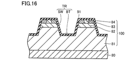
<工程S4>
次に図16を参照して、トレンチTRの側壁SWと底部BTとを覆うゲート絶縁膜91を形成する工程S4を実行することができる。ゲート絶縁膜91は、たとえば熱酸化により形成することができる。
次に図16を参照して、トレンチTRの側壁SWと底部BTとを覆うゲート絶縁膜91を形成する工程S4を実行することができる。ゲート絶縁膜91は、たとえば熱酸化により形成することができる。
<工程S51>
上記のように本実施形態において、側壁SW(第1の側壁SW1および第2のSW2)の開口方向は、Si面側またはC面側のいずれの方向であってもよい。ここで、側壁SWの開口方向がSi面側である場合は、ゲート絶縁膜91が形成された後に、炭化珪素オフ基板101とゲート絶縁膜91との界面に水素を導入する工程S51が実行されることが好ましい。
上記のように本実施形態において、側壁SW(第1の側壁SW1および第2のSW2)の開口方向は、Si面側またはC面側のいずれの方向であってもよい。ここで、側壁SWの開口方向がSi面側である場合は、ゲート絶縁膜91が形成された後に、炭化珪素オフ基板101とゲート絶縁膜91との界面に水素を導入する工程S51が実行されることが好ましい。
具体的には、雰囲気ガスとして水素(H2)ガスを用いた熱処理(以下「水素アニール」とも記す)が行なわれることが好ましい。水素アニールの熱処理条件としては、たとえば熱処理温度を1100℃以上1300℃以下、熱処理時間を1時間程度とする条件を用いることができる。これにより、炭化珪素オフ基板101とゲート絶縁膜91との界面に水素を導入することができる。水素が導入されることにより、C面に近似した特性を有する側壁SWとゲート絶縁膜91との界面おいて、界面準位の形成が抑制され、半導体装置においてチャネル移動度が向上する。なおこの熱処理では水素ガスの代わりに水蒸気もしくは水蒸気含有酸素ガスを雰囲気ガスとして用いることもできる。
<工程S52>
また、側壁SWの開口方向がC面側である場合、ゲート絶縁膜91が形成された後に、炭化珪素オフ基板101とゲート絶縁膜91との界面に窒素を導入する工程S52が実行されることが好ましい。
また、側壁SWの開口方向がC面側である場合、ゲート絶縁膜91が形成された後に、炭化珪素オフ基板101とゲート絶縁膜91との界面に窒素を導入する工程S52が実行されることが好ましい。
具体的には、雰囲気ガスとして一酸化窒素(NO)ガスを用いた熱処理(以下「窒素アニール」とも記す)が行なわれることが好ましい。窒素アニールの熱処理条件としては、たとえば熱処理温度を1100℃以上1300℃以下、熱処理時間を1時間程度とする条件を用いることができる。これにより、炭化珪素オフ基板101とゲート絶縁膜91との界面に窒素を導入することができる。窒素が導入されることにより、Si面に近似した特性を有する側壁SWとゲート絶縁膜91との界面おいて、界面準位の形成が抑制され、半導体装置においてチャネル移動度が向上する。なおこの熱処理では、NOガスの代わりにN2とO2の混合ガス、N2Oガス等を雰囲気ガスとして用いることもできる。
また、上記の水素アニールまたは窒素アニールの後に、不活性ガスを用いた熱処理が行なわれてもよい。たとえば、Arガス雰囲気下で熱処理(以下「Arアニール」とも記す)が行なわれてもよい。Arアニールの熱処理温度は、上記水素アニールまたは窒素アニールの熱処理温度よりも高く、ゲート絶縁膜91の融点よりも低いことが好ましい。熱処理時間は、たとえば1時間程度である。Arアニールを行なうことにより、界面準位の形成がさらに抑制される。
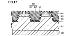
以上の工程を経た後、図17に示すように、ゲート絶縁膜91上にゲート電極92が形成される。具体的には、トレンチTRの内部の領域をゲート絶縁膜91を介して埋めるように、ゲート絶縁膜91上にゲート電極92が形成される。ゲート電極92の形成は、たとえば導体またはポリドープシリコンの成膜とCMP(Chemical Mechanical Polishing)によって行なうことができる。
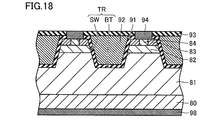
次に、図18を参照して、ゲート電極92の露出面を覆うように、ゲート電極92およびゲート絶縁膜91上に層間絶縁膜93が形成される。続いて、層間絶縁膜93およびゲート絶縁膜91に開口部が形成されるようにエッチングが行なわれる。この開口部によってn+層83およびpコンタクト領域84が露出される。そして、露出したn+層83およびpコンタクト領域84のそれぞれに接してソース電極94が形成される。さらに単結晶層80において、nドリフト層81が形成された主面側と反対側の裏面上にドレイン電極98が形成される。
そして再び図1を参照して、ソース電極94上にソース配線層95が形成される。以上のようにして、トレンチTRの互いに対向する第1の側壁SW1および第2の側壁SW2にほぼ等価な面が表出し、信頼性が高い炭化珪素半導体装置が製造される。また、この製造方法においては、トレンチTRの配置が炭化珪素オフ基板101のオフ方向に依存しない。したがって設計上の自由度が高く、炭化珪素半導体装置を高集積化することができる。
今回開示された実施形態はすべての点で例示であって制限的なものではないと解されるべきである。本発明の範囲は上記した説明ではなくて請求の範囲によって示され、請求の範囲と均等の意味および範囲内でのすべての変更が含まれることが意図される。
40,61 マスク層、60 レジスト膜、80 単結晶層、81 nドリフト層、82 pボディ層、83 n+層、84 pコンタクト領域、91 ゲート絶縁膜、92 ゲート電極、93 層間絶縁膜、94 ソース電極、95 ソース配線層、98 ドレイン電極、100 炭化珪素層、101 炭化珪素オフ基板、201 炭化珪素半導体装置、MP 主表面、TR,TQ トレンチ、SW 側壁、SW1 第1の側壁、SW2 第2の側壁、BT 底部、θ,θ1,θ2 角度、d1,d2 深さ。
Claims (14)
- 基底面に対するオフ角度を有する主表面を含む炭化珪素オフ基板を備え、
前記主表面には、トレンチが設けられ、
前記トレンチは、複数の側壁と底部とを有し、さらに、
前記側壁と前記底部とを覆うゲート絶縁膜と、
前記ゲート絶縁膜上に設けられたゲート電極と、を備え、
前記トレンチにおける前記側壁の前記基底面に対する角度が、65°を超え80°以下であり、
複数の前記側壁の開口方向が、シリコン面側またはカーボン面側のいずれかに揃っている、炭化珪素半導体装置。 - 前記炭化珪素オフ基板は、オフ方向が<11-20>方向である、請求項1に記載の炭化珪素半導体装置。
- 前記炭化珪素オフ基板の前記オフ角度は、1°以上8°以下である、請求項1または請求項2に記載の炭化珪素半導体装置。
- 前記トレンチは、複数の前記側壁が連なることにより、平面視において閉じた形状を有しており、すべての前記側壁が前記ゲート絶縁膜に覆われている、請求項1~請求項3のいずれか1項に記載の炭化珪素半導体装置。
- 複数の前記側壁は互いに対向する第1の側壁および第2の側壁を含み、
前記第1の側壁の前記基底面に対する角度と、前記第2の側壁の前記基底面に対する角度との差異は、前記オフ角度以下である、請求項1~請求項4のいずれか1項に記載の炭化珪素半導体装置。 - 複数の前記側壁の開口方向が、すべてシリコン面側である、請求項1~請求項5のいずれか1項に記載の炭化珪素半導体装置。
- 前記炭化珪素オフ基板と前記ゲート絶縁膜との界面から10nm以内の領域における水素濃度が、1×10¹⁸/cm3以上である、請求項6に記載の炭化珪素半導体装置。
- 複数の前記側壁の開口方向が、すべてカーボン面側である、請求項1~請求項5のいずれか1項に記載の炭化珪素半導体装置。
- 前記炭化珪素オフ基板と前記ゲート絶縁膜との界面から10nm以内の領域における窒素濃度が、1×10¹⁸/cm3以上である、請求項8に記載の炭化珪素半導体装置。
- 主表面を有する炭化珪素オフ基板を準備する工程と、
前記主表面に対して、異方性のエッチングを行なうことにより、側壁と底部とを有するトレンチを形成する第1のエッチング工程と、
前記側壁および前記底部に対して、等方性のエッチングを行なうことにより、前記側壁の基底面に対する角度を65°を超え80°以下とする第2のエッチング工程と、を備える、炭化珪素半導体装置の製造方法。 - 前記第1のエッチング工程により除去される前記炭化珪素オフ基板の除去深さが、前記第2のエッチング工程により除去される前記炭化珪素オフ基板の除去深さよりも深い、請求項10に記載の炭化珪素半導体装置の製造方法。
- 前記第1のエッチング工程は、前記側壁の前記基底面に対する角度が80°以上となるように、前記主表面をエッチングする工程を含む、請求項10または請求項11に記載の炭化珪素半導体装置の製造方法。
- 前記側壁の開口方向は、シリコン面側であり、
前記側壁と前記底部とを覆うゲート絶縁膜を形成する工程と、
前記炭化珪素オフ基板と前記ゲート絶縁膜との界面に水素を導入する工程と、をさらに備える、請求項10~請求項12のいずれか1項に記載の炭化珪素半導体装置の製造方法。 - 前記側壁の開口方向は、カーボン面側であり、
前記側壁と前記底部とを覆うゲート絶縁膜を形成する工程と、
前記炭化珪素オフ基板と前記ゲート絶縁膜との界面に窒素を導入する工程と、をさらに備える、請求項10~請求項12のいずれか1項に記載の炭化珪素半導体装置の製造方法。
Priority Applications (1)
| Application Number | Priority Date | Filing Date | Title |
|---|---|---|---|
| US14/912,433 US10014376B2 (en) | 2013-09-06 | 2014-07-16 | Silicon carbide semiconductor device having a trench with side walls and method for manufacturing same |
Applications Claiming Priority (2)
| Application Number | Priority Date | Filing Date | Title |
|---|---|---|---|
| JP2013184813A JP6098447B2 (ja) | 2013-09-06 | 2013-09-06 | 炭化珪素半導体装置およびその製造方法 |
| JP2013-184813 | 2013-09-06 |
Publications (1)
| Publication Number | Publication Date |
|---|---|
| WO2015033674A1 true WO2015033674A1 (ja) | 2015-03-12 |
Family
ID=52628161
Family Applications (1)
| Application Number | Title | Priority Date | Filing Date |
|---|---|---|---|
| PCT/JP2014/068881 WO2015033674A1 (ja) | 2013-09-06 | 2014-07-16 | 炭化珪素半導体装置およびその製造方法 |
Country Status (3)
| Country | Link |
|---|---|
| US (1) | US10014376B2 (ja) |
| JP (1) | JP6098447B2 (ja) |
| WO (1) | WO2015033674A1 (ja) |
Cited By (1)
| Publication number | Priority date | Publication date | Assignee | Title |
|---|---|---|---|---|
| CN113078050A (zh) * | 2021-03-30 | 2021-07-06 | 芜湖启迪半导体有限公司 | 一种C面SiC外延结构及外延沟槽的填充方法 |
Families Citing this family (6)
| Publication number | Priority date | Publication date | Assignee | Title |
|---|---|---|---|---|
| JP2016213419A (ja) | 2015-05-13 | 2016-12-15 | 住友電気工業株式会社 | 炭化珪素半導体装置 |
| FR3038127B1 (fr) * | 2015-06-24 | 2017-06-23 | Commissariat Energie Atomique | Procede de fabrication d'une pluralite de dipoles en forme d'ilots ayant des electrodes auto-alignees |
| DE102016226237A1 (de) | 2016-02-01 | 2017-08-03 | Fuji Electric Co., Ltd. | Siliziumcarbid-halbleitervorrichtung und verfahren zum herstellen einer siliziumcarbid-halbleitervorrichtung |
| JP6115678B1 (ja) | 2016-02-01 | 2017-04-19 | 富士電機株式会社 | 炭化珪素半導体装置および炭化珪素半導体装置の製造方法 |
| CN108735795B (zh) * | 2017-04-21 | 2021-09-03 | 苏州能屋电子科技有限公司 | (0001)面外延的六方相SiC晶圆、UMOSFET器件及其制作方法 |
| WO2022200338A1 (en) | 2021-03-22 | 2022-09-29 | Hitachi Energy Switzerland Ag | Power semiconductor device |
Citations (4)
| Publication number | Priority date | Publication date | Assignee | Title |
|---|---|---|---|---|
| JP2007080971A (ja) * | 2005-09-12 | 2007-03-29 | Fuji Electric Holdings Co Ltd | 半導体素子およびその製造方法 |
| JP2008235546A (ja) * | 2007-03-20 | 2008-10-02 | Denso Corp | 炭化珪素半導体装置およびその製造方法 |
| JP2009158933A (ja) * | 2007-12-04 | 2009-07-16 | Sumitomo Electric Ind Ltd | 炭化ケイ素半導体装置およびその製造方法 |
| WO2013038860A1 (ja) * | 2011-09-14 | 2013-03-21 | 住友電気工業株式会社 | 炭化珪素半導体装置およびその製造方法 |
Family Cites Families (8)
| Publication number | Priority date | Publication date | Assignee | Title |
|---|---|---|---|---|
| JP4046140B1 (ja) * | 2006-11-29 | 2008-02-13 | 住友電気工業株式会社 | 炭化珪素半導体装置の製造方法 |
| JP2008244455A (ja) * | 2007-02-28 | 2008-10-09 | Denso Corp | 炭化珪素半導体装置およびその製造方法 |
| TW201108388A (en) * | 2009-04-10 | 2011-03-01 | Sumitomo Electric Industries | Insulated gate field effect transistor |
| JP5721351B2 (ja) * | 2009-07-21 | 2015-05-20 | ローム株式会社 | 半導体装置 |
| US8981384B2 (en) * | 2010-08-03 | 2015-03-17 | Sumitomo Electric Industries, Ltd. | Semiconductor device and method for manufacturing same |
| JP2012146921A (ja) * | 2011-01-14 | 2012-08-02 | Denso Corp | 炭化珪素半導体装置 |
| KR101584023B1 (ko) * | 2011-08-26 | 2016-01-08 | 고쿠리츠다이가쿠호징 나라 센탄카가쿠기쥬츠 다이가쿠인 다이가쿠 | SiC반도체소자 및 그 제조방법 |
| US8872280B2 (en) * | 2012-07-31 | 2014-10-28 | United Microelectronics Corp. | Non-planar FET and manufacturing method thereof |
-
2013
- 2013-09-06 JP JP2013184813A patent/JP6098447B2/ja active Active
-
2014
- 2014-07-16 WO PCT/JP2014/068881 patent/WO2015033674A1/ja active Application Filing
- 2014-07-16 US US14/912,433 patent/US10014376B2/en active Active
Patent Citations (4)
| Publication number | Priority date | Publication date | Assignee | Title |
|---|---|---|---|---|
| JP2007080971A (ja) * | 2005-09-12 | 2007-03-29 | Fuji Electric Holdings Co Ltd | 半導体素子およびその製造方法 |
| JP2008235546A (ja) * | 2007-03-20 | 2008-10-02 | Denso Corp | 炭化珪素半導体装置およびその製造方法 |
| JP2009158933A (ja) * | 2007-12-04 | 2009-07-16 | Sumitomo Electric Ind Ltd | 炭化ケイ素半導体装置およびその製造方法 |
| WO2013038860A1 (ja) * | 2011-09-14 | 2013-03-21 | 住友電気工業株式会社 | 炭化珪素半導体装置およびその製造方法 |
Cited By (2)
| Publication number | Priority date | Publication date | Assignee | Title |
|---|---|---|---|---|
| CN113078050A (zh) * | 2021-03-30 | 2021-07-06 | 芜湖启迪半导体有限公司 | 一种C面SiC外延结构及外延沟槽的填充方法 |
| CN113078050B (zh) * | 2021-03-30 | 2023-03-10 | 安徽长飞先进半导体有限公司 | 一种C面SiC外延结构及外延沟槽的填充方法 |
Also Published As
| Publication number | Publication date |
|---|---|
| US10014376B2 (en) | 2018-07-03 |
| JP2015053359A (ja) | 2015-03-19 |
| US20160204206A1 (en) | 2016-07-14 |
| JP6098447B2 (ja) | 2017-03-22 |
Similar Documents
| Publication | Publication Date | Title |
|---|---|---|
| JP6098447B2 (ja) | 炭化珪素半導体装置およびその製造方法 | |
| JP5699878B2 (ja) | 炭化珪素半導体装置およびその製造方法 | |
| WO2015040966A1 (ja) | 炭化珪素半導体装置および炭化珪素半導体装置の製造方法 | |
| TW201304146A (zh) | 半導體裝置及其製造方法 | |
| JP2016066669A (ja) | 炭化珪素半導体装置の製造方法および炭化珪素半導体装置 | |
| US9799515B2 (en) | Silicon carbide semiconductor device and method of manufacturing the same | |
| WO2014199748A1 (ja) | 炭化珪素半導体装置 | |
| US20150279967A1 (en) | Method for manufacturing silicon carbide semiconductor device | |
| JP6135383B2 (ja) | 炭化珪素半導体装置 | |
| US8927368B2 (en) | Method for manufacturing silicon carbide semiconductor device | |
| JP6287193B2 (ja) | 炭化珪素半導体装置の製造方法 | |
| JP6183224B2 (ja) | 炭化珪素半導体装置の製造方法 | |
| JP2014056882A (ja) | 炭化珪素半導体装置およびその製造方法 | |
| JP6098474B2 (ja) | 炭化珪素半導体装置およびその製造方法 | |
| US9793365B2 (en) | Method for manufacturing silicon carbide semiconductor device having trench | |
| WO2015049925A1 (ja) | 炭化珪素半導体装置およびその製造方法 | |
| WO2015037335A1 (ja) | 炭化珪素半導体装置およびその製造方法 | |
| JP5870898B2 (ja) | 炭化珪素半導体装置 | |
| JP2019012801A (ja) | 炭化珪素半導体装置の製造方法 |
Legal Events
| Date | Code | Title | Description |
|---|---|---|---|
| 121 | Ep: the epo has been informed by wipo that ep was designated in this application |
Ref document number: 14842749 Country of ref document: EP Kind code of ref document: A1 |
|
| WWE | Wipo information: entry into national phase |
Ref document number: 14912433 Country of ref document: US |
|
| NENP | Non-entry into the national phase |
Ref country code: DE |
|
| 122 | Ep: pct application non-entry in european phase |
Ref document number: 14842749 Country of ref document: EP Kind code of ref document: A1 |