WO2015030191A1 - マイクロ波プラズマ処理装置 - Google Patents
マイクロ波プラズマ処理装置 Download PDFInfo
- Publication number
- WO2015030191A1 WO2015030191A1 PCT/JP2014/072779 JP2014072779W WO2015030191A1 WO 2015030191 A1 WO2015030191 A1 WO 2015030191A1 JP 2014072779 W JP2014072779 W JP 2014072779W WO 2015030191 A1 WO2015030191 A1 WO 2015030191A1
- Authority
- WO
- WIPO (PCT)
- Prior art keywords
- gas
- gas flow
- microwave
- plasma
- dielectric substrate
- Prior art date
- Legal status (The legal status is an assumption and is not a legal conclusion. Google has not performed a legal analysis and makes no representation as to the accuracy of the status listed.)
- Ceased
Links
Images








Classifications
-
- H—ELECTRICITY
- H01—ELECTRIC ELEMENTS
- H01J—ELECTRIC DISCHARGE TUBES OR DISCHARGE LAMPS
- H01J37/00—Discharge tubes with provision for introducing objects or material to be exposed to the discharge, e.g. for the purpose of examination or processing thereof
- H01J37/32—Gas-filled discharge tubes
- H01J37/32009—Arrangements for generation of plasma specially adapted for examination or treatment of objects, e.g. plasma sources
- H01J37/32192—Microwave generated discharge
-
- C—CHEMISTRY; METALLURGY
- C23—COATING METALLIC MATERIAL; COATING MATERIAL WITH METALLIC MATERIAL; CHEMICAL SURFACE TREATMENT; DIFFUSION TREATMENT OF METALLIC MATERIAL; COATING BY VACUUM EVAPORATION, BY SPUTTERING, BY ION IMPLANTATION OR BY CHEMICAL VAPOUR DEPOSITION, IN GENERAL; INHIBITING CORROSION OF METALLIC MATERIAL OR INCRUSTATION IN GENERAL
- C23C—COATING METALLIC MATERIAL; COATING MATERIAL WITH METALLIC MATERIAL; SURFACE TREATMENT OF METALLIC MATERIAL BY DIFFUSION INTO THE SURFACE, BY CHEMICAL CONVERSION OR SUBSTITUTION; COATING BY VACUUM EVAPORATION, BY SPUTTERING, BY ION IMPLANTATION OR BY CHEMICAL VAPOUR DEPOSITION, IN GENERAL
- C23C16/00—Chemical coating by decomposition of gaseous compounds, without leaving reaction products of surface material in the coating, i.e. chemical vapour deposition [CVD] processes
- C23C16/44—Chemical coating by decomposition of gaseous compounds, without leaving reaction products of surface material in the coating, i.e. chemical vapour deposition [CVD] processes characterised by the method of coating
- C23C16/455—Chemical coating by decomposition of gaseous compounds, without leaving reaction products of surface material in the coating, i.e. chemical vapour deposition [CVD] processes characterised by the method of coating characterised by the method used for introducing gases into reaction chamber or for modifying gas flows in reaction chamber
-
- C—CHEMISTRY; METALLURGY
- C23—COATING METALLIC MATERIAL; COATING MATERIAL WITH METALLIC MATERIAL; CHEMICAL SURFACE TREATMENT; DIFFUSION TREATMENT OF METALLIC MATERIAL; COATING BY VACUUM EVAPORATION, BY SPUTTERING, BY ION IMPLANTATION OR BY CHEMICAL VAPOUR DEPOSITION, IN GENERAL; INHIBITING CORROSION OF METALLIC MATERIAL OR INCRUSTATION IN GENERAL
- C23C—COATING METALLIC MATERIAL; COATING MATERIAL WITH METALLIC MATERIAL; SURFACE TREATMENT OF METALLIC MATERIAL BY DIFFUSION INTO THE SURFACE, BY CHEMICAL CONVERSION OR SUBSTITUTION; COATING BY VACUUM EVAPORATION, BY SPUTTERING, BY ION IMPLANTATION OR BY CHEMICAL VAPOUR DEPOSITION, IN GENERAL
- C23C16/00—Chemical coating by decomposition of gaseous compounds, without leaving reaction products of surface material in the coating, i.e. chemical vapour deposition [CVD] processes
- C23C16/44—Chemical coating by decomposition of gaseous compounds, without leaving reaction products of surface material in the coating, i.e. chemical vapour deposition [CVD] processes characterised by the method of coating
- C23C16/455—Chemical coating by decomposition of gaseous compounds, without leaving reaction products of surface material in the coating, i.e. chemical vapour deposition [CVD] processes characterised by the method of coating characterised by the method used for introducing gases into reaction chamber or for modifying gas flows in reaction chamber
- C23C16/45563—Gas nozzles
-
- C—CHEMISTRY; METALLURGY
- C23—COATING METALLIC MATERIAL; COATING MATERIAL WITH METALLIC MATERIAL; CHEMICAL SURFACE TREATMENT; DIFFUSION TREATMENT OF METALLIC MATERIAL; COATING BY VACUUM EVAPORATION, BY SPUTTERING, BY ION IMPLANTATION OR BY CHEMICAL VAPOUR DEPOSITION, IN GENERAL; INHIBITING CORROSION OF METALLIC MATERIAL OR INCRUSTATION IN GENERAL
- C23C—COATING METALLIC MATERIAL; COATING MATERIAL WITH METALLIC MATERIAL; SURFACE TREATMENT OF METALLIC MATERIAL BY DIFFUSION INTO THE SURFACE, BY CHEMICAL CONVERSION OR SUBSTITUTION; COATING BY VACUUM EVAPORATION, BY SPUTTERING, BY ION IMPLANTATION OR BY CHEMICAL VAPOUR DEPOSITION, IN GENERAL
- C23C16/00—Chemical coating by decomposition of gaseous compounds, without leaving reaction products of surface material in the coating, i.e. chemical vapour deposition [CVD] processes
- C23C16/44—Chemical coating by decomposition of gaseous compounds, without leaving reaction products of surface material in the coating, i.e. chemical vapour deposition [CVD] processes characterised by the method of coating
- C23C16/50—Chemical coating by decomposition of gaseous compounds, without leaving reaction products of surface material in the coating, i.e. chemical vapour deposition [CVD] processes characterised by the method of coating using electric discharges
- C23C16/511—Chemical coating by decomposition of gaseous compounds, without leaving reaction products of surface material in the coating, i.e. chemical vapour deposition [CVD] processes characterised by the method of coating using electric discharges using microwave discharges
-
- C—CHEMISTRY; METALLURGY
- C23—COATING METALLIC MATERIAL; COATING MATERIAL WITH METALLIC MATERIAL; CHEMICAL SURFACE TREATMENT; DIFFUSION TREATMENT OF METALLIC MATERIAL; COATING BY VACUUM EVAPORATION, BY SPUTTERING, BY ION IMPLANTATION OR BY CHEMICAL VAPOUR DEPOSITION, IN GENERAL; INHIBITING CORROSION OF METALLIC MATERIAL OR INCRUSTATION IN GENERAL
- C23C—COATING METALLIC MATERIAL; COATING MATERIAL WITH METALLIC MATERIAL; SURFACE TREATMENT OF METALLIC MATERIAL BY DIFFUSION INTO THE SURFACE, BY CHEMICAL CONVERSION OR SUBSTITUTION; COATING BY VACUUM EVAPORATION, BY SPUTTERING, BY ION IMPLANTATION OR BY CHEMICAL VAPOUR DEPOSITION, IN GENERAL
- C23C16/00—Chemical coating by decomposition of gaseous compounds, without leaving reaction products of surface material in the coating, i.e. chemical vapour deposition [CVD] processes
- C23C16/44—Chemical coating by decomposition of gaseous compounds, without leaving reaction products of surface material in the coating, i.e. chemical vapour deposition [CVD] processes characterised by the method of coating
- C23C16/50—Chemical coating by decomposition of gaseous compounds, without leaving reaction products of surface material in the coating, i.e. chemical vapour deposition [CVD] processes characterised by the method of coating using electric discharges
- C23C16/513—Chemical coating by decomposition of gaseous compounds, without leaving reaction products of surface material in the coating, i.e. chemical vapour deposition [CVD] processes characterised by the method of coating using electric discharges using plasma jets
-
- H—ELECTRICITY
- H01—ELECTRIC ELEMENTS
- H01J—ELECTRIC DISCHARGE TUBES OR DISCHARGE LAMPS
- H01J37/00—Discharge tubes with provision for introducing objects or material to be exposed to the discharge, e.g. for the purpose of examination or processing thereof
- H01J37/32—Gas-filled discharge tubes
- H01J37/32431—Constructional details of the reactor
- H01J37/3244—Gas supply means
-
- H—ELECTRICITY
- H05—ELECTRIC TECHNIQUES NOT OTHERWISE PROVIDED FOR
- H05H—PLASMA TECHNIQUE; PRODUCTION OF ACCELERATED ELECTRICALLY-CHARGED PARTICLES OR OF NEUTRONS; PRODUCTION OR ACCELERATION OF NEUTRAL MOLECULAR OR ATOMIC BEAMS
- H05H1/00—Generating plasma; Handling plasma
- H05H1/24—Generating plasma
- H05H1/46—Generating plasma using applied electromagnetic fields, e.g. high frequency or microwave energy
-
- H—ELECTRICITY
- H05—ELECTRIC TECHNIQUES NOT OTHERWISE PROVIDED FOR
- H05H—PLASMA TECHNIQUE; PRODUCTION OF ACCELERATED ELECTRICALLY-CHARGED PARTICLES OR OF NEUTRONS; PRODUCTION OR ACCELERATION OF NEUTRAL MOLECULAR OR ATOMIC BEAMS
- H05H1/00—Generating plasma; Handling plasma
- H05H1/24—Generating plasma
- H05H1/46—Generating plasma using applied electromagnetic fields, e.g. high frequency or microwave energy
- H05H1/461—Microwave discharges
- H05H1/4622—Microwave discharges using waveguides
-
- H—ELECTRICITY
- H01—ELECTRIC ELEMENTS
- H01J—ELECTRIC DISCHARGE TUBES OR DISCHARGE LAMPS
- H01J2237/00—Discharge tubes exposing object to beam, e.g. for analysis treatment, etching, imaging
- H01J2237/32—Processing objects by plasma generation
- H01J2237/33—Processing objects by plasma generation characterised by the type of processing
- H01J2237/332—Coating
-
- H—ELECTRICITY
- H01—ELECTRIC ELEMENTS
- H01J—ELECTRIC DISCHARGE TUBES OR DISCHARGE LAMPS
- H01J2237/00—Discharge tubes exposing object to beam, e.g. for analysis treatment, etching, imaging
- H01J2237/32—Processing objects by plasma generation
- H01J2237/33—Processing objects by plasma generation characterised by the type of processing
- H01J2237/334—Etching
Definitions
- plasma is generated by microwave power, and a processing target such as a wafer is subjected to processing such as CVD (chemical vapor synthesis), etching, ashing (resist ashing), plasma nitriding, etc. using plasma.
- CVD chemical vapor synthesis
- etching etching
- ashing ashing
- plasma nitriding etc. using plasma.
- the present invention relates to a microwave plasma processing apparatus.
- Plasma processing technology has become indispensable in many fields such as material development and production technology.
- Plasma is widely used in low-temperature dry process technology because it can generate high-density radicals while having high non-thermal equilibrium.
- a plasma jet has been used as one of plasma sources under a pressure between an intermediate pressure (1 to 100 torr) and an atmospheric pressure. Since the plasma jet blows plasma from the nozzle of the apparatus, the substrate to be processed such as a wafer is subjected to processing such as CVD (chemical vapor synthesis) using plasma, etching, ashing (resist ashing treatment), plasma nitriding, It is useful.
- CVD chemical vapor synthesis
- etching etching
- ashing resist ashing treatment
- plasma nitriding It is useful.
- a method using DC arc discharge or DC pulse discharge is well known for generating a plasma jet.
- the method using direct-current arc discharge or direct-current pulse discharge has various problems such as the electrode being easily deteriorated and the inability to use reactive gas.
- a method using dielectric barrier discharge is well known.
- the method using the dielectric barrier discharge has various problems such as generation of filament-like discharge and generation of high-density radicals.
- an electrodeless plasma jet generator is known.
- an inductively coupled thermal plasma generator using a high frequency in the VHF band (30 to 300 MHz) has been proposed (see Patent Document 1).
- the proposed plasma jet generator is complicated in impedance matching, cannot be scaled up due to structural problems, and uses a high-voltage electric circuit. Has limitations and problems.
- generating a plasma jet using microwave discharge has the following advantages.
- Microwave power supply is cheap.
- Electrodeless operation is possible and the discharge sustaining life is long.
- Impedance matching is possible with simple elements.
- Good microwave and plasma coupling efficiency There is little radiation loss to the outside, and power can be concentrated where necessary.
- Stable high-density plasma is generated in a wide pressure range including atmospheric pressure.
- the conventional plasma generator using microwave power uses a waveguide, which is a metal tube, as the microwave transmission line, and the structure of the microwave transmission circuit becomes large and expensive, and the operation is performed with low power. Is difficult.
- Patent Document 2 a method of manufacturing a plasma jet generation device using a microstrip line, which is a microwave transmission line for low power, instead of a conventional waveguide has been proposed (Patent Document 2 and Non-Patent Document 1). reference).
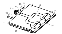
- FIG. 19 shows a schematic diagram of a plasma jet generator using a conventional microstrip line.
- This apparatus includes a microwave input unit 31, a dielectric substrate 1 having a tapered structure at one end and a gas flow path therein, a microwave strip line 11 for microwave power transmission, and one surface of the dielectric substrate. It is composed of an earth conductor 12 to cover.
- the gas is input from the two gas input ports 21, passes through the gas flow path 22, and merges between the microstrip line 11 and the ground conductor 12 at the tapered portion 14, and the dielectric substrate 1 from the nozzle 24 having a width of 10 mm. Blows outside.
- gas input ports 21 are provided on both side surfaces of the dielectric substrate 1, and the gas passes through the oblique gas flow paths 22. Supply.
- Microwave (2.45 GHz) power is introduced into the dielectric substrate 1 through the coaxial microwave connect 31, propagates between the microstrip line 11 and the ground conductor 12, and concentrates at the nozzle 24. . Thereby, plasma is generated and blown out of the dielectric substrate 1 from the nozzle 24 together with the gas flow.
- the present invention provides a microwave plasma processing apparatus capable of stably generating a low-temperature and wide-width plasma jet not only at low pressure but also at high pressure from intermediate pressure to atmospheric pressure. For the purpose.
- the microwave plasma processing apparatus of the present invention includes a dielectric substrate, a tapered portion provided at one end portion of the dielectric substrate, the tapered portion having a shape in which the thickness of the dielectric substrate gradually decreases, and the dielectric substrate.
- a microstrip line provided from one end of the first surface, which is one of the front surface and the back surface, to the other end, and opposite to the first surface of the dielectric substrate
- a ground conductor provided from one end of the second surface to the other end of the second surface, and at one end of the dielectric substrate, the microstrip line and the ground conductor
- a microwave input unit for inputting a microwave in between, a gas input port for inputting a gas into the dielectric substrate, and a plasma generated by the microwave input from the microwave input unit Space, or
- a plasma generating portion which is a space provided in the dielectric substrate of the tapered portion, and a wide gas flow having a uniform flow velocity to the plasma generating portion.
- a gas flow widening portion formed so that the gas flow width becomes wider as the gas flow proceeds, and a gas flow path for supplying the gas input from the gas input port to the gas flow widening portion And a nozzle for blowing out the gas supplied to the plasma generation unit and the plasma generated by the microwave.
- the microwave plasma processing apparatus of the present invention includes a dielectric substrate, a tapered portion provided at one end of the dielectric substrate and having a shape in which the thickness of the dielectric substrate gradually decreases, and the dielectric A microstrip line provided from one end of the first surface, which is one of the front and back surfaces of the substrate, to the other end; and the first surface of the dielectric substrate A ground conductor provided from one end of the second surface to the other end of the second surface, and at one end of the dielectric substrate, the microstrip line and the ground conductor A space between the end of the ground conductor and the end of the microstrip line in the taper portion, and a microwave input portion for inputting a microwave between the first and second portions of the dielectric substrate.
- a gas supply plate having a gas flow widening portion formed as described above, a gas input port for inputting gas into the gas supply plate, and a gas input from the gas input port in the gas supply plate.
- the gas for generating plasma by the microwave radiated from the gap of the microwave concentration from the gas flow path for supplying to the gas flow widening section and the gas supplied from the gas flow widening section Plasma generated by a microwave from a gas supplied to the plasma generator, which is a space facing the gap between the microwaves formed on the supply plate, and a gas supplied to the plasma generator is discharged.
- the nozzle, further comprising a are the main features.
- the gas flow widening portion is formed with a plurality of protruding obstacles or columns provided at regular intervals along the major axis direction of the nozzle.
- the main feature is that it is provided with a gas shower part, which is a part that has been made.
- the microstrip line has one input end provided at one end portion, a branching portion that branches the microwave input from the input end, A plurality of lines separated from the branching section and a plurality of output ends provided at the other end corresponding to the plurality of lines, and by gradually reducing the width of the other end, the impedance
- the main feature is that the microwave electric field in the plasma generating section is increased.
- the gas flow widening unit includes one input end provided at one end, and a branch unit that branches the gas flow input from the gas flow path.
- the plurality of lines formed so that the width gradually increases so that the width of the gas flow increases as the gas flow progresses, and the gas flow flowing from the plurality of lines merges into one.
- the main feature is that it has a long-axis shaped space.
- the microwave plasma processing apparatus of the present invention is characterized in that it is configured to generate plasma having a long major axis by arranging the dielectric substrate and the ground conductor in common and arranging them side by side. Yes.
- the microwave plasma processing apparatus of the present invention supplies a rare gas, a reactive gas, or a mixed gas of a rare gas and a reactive gas, and generates plasma at a low pressure, an intermediate pressure, or a high pressure. This is the main feature.
- the present invention it is possible to generate and maintain a stable and wide plasma jet not only at a low pressure but also at an intermediate pressure and a high pressure.
- a microwave-excited plasma jet having a wide width at atmospheric pressure (or low or intermediate pressure)
- Material processing such as CVD (Chemical Vapor Deposition) film formation becomes possible.
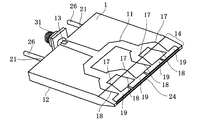
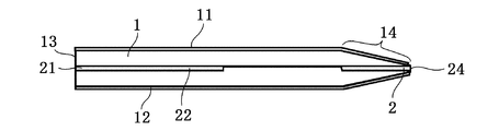
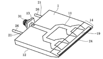
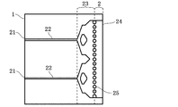
- the perspective view of the plasma processing apparatus which shows one of the Examples of the 1st Embodiment of this invention 1 is a vertical sectional view of the plasma processing apparatus shown in FIG. 1 is a horizontal sectional view of the plasma processing apparatus shown in FIG. Configuration diagram of the microstrip line of the present invention
- the schematic diagram of the plasma processing apparatus which shows one of the Examples of the 1st Embodiment of this invention The schematic diagram of the plasma processing apparatus which shows one of the Examples of 1st Embodiment in this invention
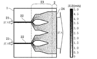
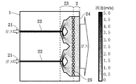
- the figure which shows the flow velocity distribution of the gas flow in the plasma processing apparatus shown in FIG. 3 is a diagram showing a flow velocity distribution of a gas flow in the major axis direction of the nozzle 24 in the plasma processing apparatus shown in FIG.
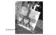
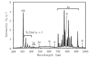
- FIG. Photograph of wide plasma jet generated in atmospheric pressure air by plasma processing apparatus showing example of second embodiment of present invention Spectral spectrum from light emission of plasma jet generated in atmospheric pressure air by plasma processing apparatus showing example of second embodiment of present invention Photograph of a wide nitrogen plasma jet generated by a plasma processing apparatus showing an example of the second embodiment of the present invention
- FIG. 15 is a vertical sectional view of the plasma processing apparatus shown in FIG.
- FIG. 15 is a horizontal sectional view of the plasma processing apparatus shown in FIG.
- Plasma processing apparatus according to third embodiment of the invention Description perspective view of a conventional plasma generator using a microstrip line
- FIG. 1, FIG. 2 and FIG. 3 are diagrams showing the configuration of one plasma processing apparatus of an example showing the first embodiment of the present invention.
- 1 is a perspective view of the plasma processing apparatus
- FIG. 2 is a vertical sectional view
- FIG. 3 is a horizontal sectional view.
- the plasma processing apparatus includes a dielectric substrate 1, a microwave input unit 13, a microstrip line 11, a ground conductor 12, a taper unit 14, a gas input port 21, a gas flow path 22, and a gas flow widening unit 23.
- the plasma generating unit 2 and the nozzle 24 are provided.
- the dielectric substrate 1 is preferably made of a material with low microwave dielectric loss and high thermal conductivity.
- an appropriate material such as alumina, quartz, sapphire, or the like is used.
- the dielectric substrate 1 may be a flexible material, for example, an appropriate material such as polystyrene or polystyrene.
- the dielectric constant and thickness of the dielectric substrate 1 affect the characteristic impedance of the microwave propagation circuit.
- a suitable dielectric substrate 1 can be used in consideration of the microwave propagation characteristics, the shape of the plasma processing apparatus, the thermal characteristics of the plasma processing apparatus, and the like.
- the dielectric substrate 1 may be a single substrate or may be a stack of a plurality of substrates.
- the dielectric substrate 1 may be a stack of a plurality of substrates made of different materials.
- the microwave input unit 13 is for exciting the microwave between the microstrip line 11 and the ground conductor 12 at one end of the dielectric substrate 1.
- SMA connect, SMB connect, N connect, BNC connect, OSM connect, etc. for microwave coaxial cables can be used.
- the microwave input unit 13 can also be configured by making a hole in the ground conductor 12 and attaching a microwave connect.
- the microstrip line 11 is provided from one end of the first surface of the dielectric substrate 1 to the other end.
- the phrase “microstrip” is used, but other conductors may be used as appropriate as long as they are for propagating microwaves.
- the shape of the microstrip line 11 is an important factor that determines characteristics such as the impedance of the microwave circuit, the electric field distribution, and the distribution ratio of the microwave power. In order to realize generation of a uniform plasma jet, it is necessary to optimize the shape of the microstrip line 11. In the design of the microwave circuit of the microstrip line 11, techniques for uniform distribution of microwave power, matching of characteristic impedance, impedance matching, and the like have already been established as wireless communication techniques, and these should be used as appropriate. Can do.
- FIG. 4 shows a configuration diagram of a microstrip line 11 which is one of the embodiments in the present invention.
- the microstrip line 11 has one input end 15 at one end, a branching portion 16 for branching the microwave input from the input end, a plurality of lines 17 separated from the branching portion 16, and a plurality of lines. 17 and a plurality of output ends 19 at the end 18 on the other output side corresponding to 17.
- a microwave transmission line is branched twice from one microwave input unit 13 and then branched into four lines 17, thereby generating a plasma generating unit having a width of 50 mm. 2 is provided so that microwave power can be supplied uniformly.
- the end 18 and the output 19 on the output side of the microstrip line 11 have a uniform spatial distribution of the microwave electric field in the plasma generator 2 (see FIG. 3) and a high electric field strength. It can be made into an appropriate shape.
- the end portion 18 of the microstrip line 11 has a shape in which the width gradually decreases, and is connected to the corresponding long-axis-shaped output end 19.
- the characteristic impedance of the microwave propagation circuit is increased.
- the voltage applied to the microstrip line 11 and the ground conductor 12 increases for a certain microwave power.
- the microwave electric field between the microstrip line 11 and the ground conductor 12 is further strengthened by the following formula 1.
- E is the electric field
- V and d are the voltage and distance between the microstrip line 11 and the ground conductor 12, respectively.
- the end of the microstrip line 11 can also be shaped so that the width of the end 18 on the output side of the microstrip line 11 gradually increases as shown in FIG.
- the output end 19 of the microstrip line 11 may be provided separately corresponding to the plurality of lines 17 branched into a plurality of lines, or the plurality of output ends 19 may be integrated into one as shown in FIG. It may be a connected shape.
- the ground conductor 12 has one end of the second surface that is the surface opposite to the first surface (surface on which the microstrip line 11 is formed) of the dielectric substrate 1. From the first part to the other end part.
- the ground conductor 12 may be composed of a conductor that covers the entire second surface of the dielectric substrate 1, or may be composed of a conductor formed on a part of the second surface.
- microstrip line 11 and the ground conductor 12 for example, an appropriate conductor material such as copper, gold, silver, aluminum, or nickel is used.
- the microstrip line 11 and the ground conductor 12 can be formed by using a normal IC manufacturing technique such as metal deposition or etching on the dielectric substrate 1.
- the microstrip line 11 and the ground conductor 12 may be made by attaching an appropriate conductor plate to the surface of the dielectric substrate 1 using an adhesive.
- the tapered portion 14 is provided by making the thickness of the dielectric substrate 1 gradually decrease at one end portion of the dielectric substrate 1.
- the tapered portion 14 may have a shape in which the slope of the slope of the first surface of the dielectric substrate 1 and the slope of the slope of the second surface are the same, or the first surface of the dielectric substrate 1 or the second surface. A shape in which a slope is provided on only one of the two surfaces may be used.
- the microwave electric field between the microstrip line 11 and the ground conductor 12 becomes stronger as the thickness of the dielectric substrate 1 becomes thinner, that is, as the distance between the microstrip line 11 and the ground conductor 12 becomes shorter. (See Equation 1). Based on this principle, the microwave electric field becomes strong in the tapered portion 14.
- the length of the tapered portion 14 is preferably set to a quarter wavelength of the microwave standing wave formed in the dielectric substrate.
- the length of the tapered portion 14 can be appropriately determined in consideration of the inclination angle of the shape of the tapered portion 14, the characteristic impedance, and the like. Further, by appropriately adjusting the inclination angle and the length of the tapered portion 14, the reflected wave of the microwave reflected from the plasma can be largely suppressed.
- the gas input port 21 and the gas flow path 22 are provided to supply a gas to the gas flow widening section 23 (FIG. 3).
- the gas input port 21 can be provided at one end of the dielectric substrate 1 or can be provided on the other surface of the dielectric substrate 1.
- the material of the gas pipe 26 and the gas connect connected to the gas input port 21 is preferably an insulator, but may be made of metal. When the metal gas pipe 26 and the gas connect are used, it is necessary to provide them at appropriate positions in consideration of the influence on the microwave propagation.
- the gas flow widening section 23 (FIG. 3) is provided to uniformly spread the gas supplied from the gas flow path 22 and supply it to the plasma generating section 2.
- the gas flow widening section 23 is divided into one input end at one end, a branch section for branching the gas flow input from the gas flow path 22, and the branch section so that the width of the gas flow is widened.
- FIG. 3 shows an embodiment relating to the gas flow widening section 23 of the present invention.
- gas is input to the gas flow path 22 from the two gas input ports 21.
- the input gas flow is branched into two at the gas flow widening section 23. Further, the width of the gas flow is gradually increased at the gas flow widening portion 23. Thereafter, the four branched gas flows merge together at the plasma generation unit 2. As a result, the gas flow can be uniformly expanded to a width of 50 mm and supplied to the plasma generator 2.
- FIG. 7 shows the result of the simulation of the gas flow velocity distribution in the gas flow widening section 23 of the embodiment shown in FIG.
- the simulation conditions are as follows: the gas type is nitrogen, the total gas flow rate into the two gas input ports 21 is 300 sccm, the ambient pressure is atmospheric pressure (760 Torr), the cross-sectional area of the gas input port 21 is 1 mm wide, and the plasma generator 2 The length of the nozzle 24 is 50 mm, and the height of the gas input port 21, the gas flow widening section 23, the plasma generation section 2 and the nozzle 24 is 0.5 mm.
- the gas input to the gas flow widening unit 23 through the gas input port 21 and the gas flow path 22 is widened to a width of 50 mm at a uniform flow rate while passing through the gas flow widening unit 23, and the plasma generation unit 2. It blows out from the nozzle 24 through the nozzle.
- the flow rate of the gas input from the gas flow path 22 to the gas flow widening section 23 is about 12.0 m / sec.
- the gas flow rate in the nozzle 24 is 0.33 to 0.35 m / sec in the major axis direction of the nozzle 24, and spreads in a uniform distribution.
- the gas flow velocity distribution with respect to the long axis of the nozzle 24 is shown in FIG.
- the flow rate of the gas input from the gas flow path 22 to the gas flow widening section 23 is large such as the gas flow rate input to the gas input port 21, the cross-sectional area of the gas flow path 22, and the pressure outside the nozzle 24. Dependent.
- gas flow widening section 23 having an appropriate shape corresponding to the maximum value of the gas flow velocity input to the gas flow widening section 23, for example, by providing the gas flow widening section 23 longer, plasma generation A uniform and wide gas flow can be supplied to the part 2 and the nozzle 24.
- the plasma generation unit 2 (FIG. 3) is a space where the gas supplied from the gas flow widening unit 23 becomes a plasma state by a microwave electric field.
- the plasma generator 2 is preferably provided as one space so that a wide plasma is uniformly generated.
- the space of the plasma generating unit 2 can be configured with a plurality of spaces in consideration of the application of the plasma processing apparatus.
- the nozzle 24 is an opening through which the plasma generated in the plasma generator 2 blows out together with the gas to the outside of the dielectric substrate 1. It is desirable to provide one nozzle 24 so that a wide plasma is blown out uniformly.
- the nozzle 24 can have an appropriate shape depending on the desired cross-sectional shape of the plasma jet.
- the electric field of the microwave gradually increases at the tapered portion 14 because the distance between the microstrip line 11 and the ground conductor 12 is narrow, and between the end of the microstrip line 11 and the end of the ground conductor 12. The maximum value is reached.
- This concentrated microwave electric field excites the gas supplied to the plasma generator, and plasma is generated.
- the generated plasma blows out from the nozzle 24 together with the gas flow. Thereby, a uniform wide plasma jet can be supplied.
- the plasma processing apparatus according to the second embodiment of the present invention is the same as the plasma processing apparatus according to the first embodiment described above. As shown in FIG. This is a device provided with a gas shower unit 25 for spreading the air.
- the gas flow path 22 can be lengthened and the gas flow widening portion 23 can be shortened.
- the gas shower unit 25 is provided by forming a plurality of protruding obstacles at regular intervals along the major axis direction of the nozzle 24.
- the gas shower unit 25 can also be provided by forming a plurality of columns at regular intervals.
- the protruding obstacles and the pillars in the gas shower unit 25 may be provided separately or may be formed by processing the dielectric substrate 1.
- the cross-sectional shape of the protruding obstacle and the column may be circular, or may be a triangle, a quadrangle, or the like.
- the distance and cross-sectional area between the protruding obstacle and the pillar are the mean free path of gas particles (the average flight distance from one gas particle colliding with another gas particle to the next collision) Value) can be determined as appropriate.
- FIG. 9 is a horizontal sectional view of the plasma processing apparatus according to the second embodiment of the present invention.
- the gas shower unit 25 provided in the plasma processing apparatus of the second exemplary embodiment processes the dielectric substrate 1 to form circular pillars having a diameter of 2 mm at intervals of 3 mm (from the center of the pillar to the center of the adjacent pillar). Provided by forming a plurality at a distance).
- FIG. 10 shows the result of the simulation of the gas flow velocity distribution in the plasma processing apparatus of the second embodiment shown in FIG.
- the gas type is nitrogen
- the total gas flow rate into the two gas input ports 21 is 400 sccm
- the ambient pressure is atmospheric pressure (760 Torr)
- the cross-sectional area of the gas input port 21 is 1 mm wide
- the plasma generator 2 The length of the nozzle 24 is 50 mm, and the height of the gas input port 21, the gas flow widening section 23, the plasma generation section 2, and the nozzle 24 is 0.5 mm.
- the circular pillars in the gas shower part had a diameter of 2 mm, and the interval between the pillars was 3 mm.
- the flow rate of the gas input from the gas flow path 22 to the gas flow widening section 23 was about 18.0 m / sec.
- the gas flow rate in the nozzle 24 is 0.44 to 0.50 m / sec in the major axis direction of the nozzle 24 and spreads uniformly.
- the gas flowing into the gas flow widening section 23 through the gas input port 21 and the gas flow path 22 is widened to a width of 50 mm at a uniform flow rate while passing through the gas flow widening section 23, It is blown out from the nozzle 24 through.
- the plasma processing apparatus can provide a wide plasma jet that is stably generated and maintained not only at a low pressure but also at an intermediate pressure and a high pressure. Next, an experiment for generating a wide plasma jet will be described.
- FIG. 11 shows a photograph of a plasma jet generated in atmospheric pressure air using the plasma processing apparatus according to the second embodiment of the present invention.
- Ar gas is used as an operating gas in order to stably generate and maintain plasma.
- a wide plasma of 50 mm is stably blown out in the atmospheric pressure.
- the flow rate of Ar gas is 0.1 L / mim to 10 L / mim
- the frequency of the microwave is 2.45 GHz
- the microwave power is 30 W to 100 W.
- a rare gas such as helium (He) or neon (Ne) may be used instead of Ar gas.
- This wide plasma jet enables various plasma treatments at atmospheric pressure.
- the surface modification (improvement of hydrophilicity, adhesion, etc.) of the substrate to be processed can be performed by blowing a plasma jet of Ar gas onto the surface of the substrate to be processed in the air.
- the surrounding air containing N 2 , O 2 , H 2 O, CO 2, etc.
- the air is turned into plasma. This is because chemically reactive species (radicals) are generated.
- FIG. 12 shows a spectral spectrum from a plasma jet of Ar gas blown into atmospheric pressure air.
- emission spectra of OH, O, N 2 excited species, and the like appear.
- OH radicals are particularly important radicals in plasma processing such as surface modification.
- the peak of the emission spectrum of the OH radical near the wavelength of 309 cm ⁇ 1 is 3.4 times that of the strongest peak (near 337 cm ⁇ 1 ) of the 2nd positive system of N 2 molecules. strong. This indicates that OH radicals are generated at a higher density than other radicals.
- an atmospheric pressure plasma jet using Ar gas or He gas as an operating gas
- the emission spectrum of OH radicals is lower than the N 2 molecule emission spectrum.
- the plasma processing apparatus of the present invention can efficiently concentrate the microwave power in the plasma generation space of the plasma generation unit using the microstrip line, and has a high density. This characteristic is obtained because of the ability to stably generate plasma.
- the Ar gas plasma jet of this example By using the Ar gas plasma jet of this example, the surface of a polycarbonate substrate, polyimide film, glass substrate, printing paper, etc. is treated in the atmosphere, and excellent experimental results such as super hydrophilicity are obtained. . In addition, a plasma ashing experiment in which the resist is peeled off in the atmosphere using the Ar gas plasma jet of this example has been confirmed, and it has been confirmed that low temperature and high speed processing can be performed.
- the plasma processing apparatus of the present invention can be operated by mixing a small amount of reaction gas with Ar gas which is an operation gas.
- Ar gas which is an operation gas.
- the treatment time is further shortened by supplying a small amount of oxygen or air to the Ar gas.
- the plasma processing apparatus of the present invention mixes and supplies a small amount of methane (CH 4 ) gas and hydrogen (H 2 ) gas at an appropriate ratio to Ar gas as an operating gas, thereby supplying a DLC (diamond like carbon) thin film. Further, it can be applied to atmospheric pressure plasma CVD for synthesizing carbon materials such as a nanocrystal diamond thin film and a graphene film.
- the plasma processing apparatus of the present invention can perform continuous processing by providing a movable substrate stage below a wide plasma jet.
- the plasma processing apparatus of the present invention can generate reactive gas plasma at low and intermediate pressures without using rare gas operating gases such as Ar gas and He gas.
- rare gas operating gases such as Ar gas and He gas.
- a rare gas operating gas such as Ar gas and He gas may be used.
- a plasma processing apparatus showing a second embodiment of the present invention was installed in a vacuum vessel, and microwave power and gas were supplied to the plasma processing apparatus through a flange.
- the gas only the N 2 gas was used without using the above operating gas.
- the gas pressure in the vacuum vessel was controlled by fixing the flow rate of N 2 gas at 500 sccm and controlling the exhaust valve of the vacuum vessel.
- FIG. 13 shows a wide plasma jet photograph generated at 10 Torr. The photo was taken from the front of the plasma jet. As can be seen from the plasma emission in the photograph, a uniform wide plasma is generated.
- FIG. 14 shows the results of examining the minimum microwave power required for plasma ignition and plasma maintenance and the pressure in the container (3 Torr to 50 Torr).
- the plasma was ignited with a microwave power of 22 W and maintained up to 13 W.
- the minimum power required for plasma ignition and plasma maintenance increased with increasing pressure in the vessel.
- the plasma was ignited with a microwave power of 52 W and maintained up to 50 W.
- the plasma processing apparatus of the present invention can generate stable nitrogen plasma with low power.
- This nitrogen plasma is expected to be applied to plasma nitriding treatments such as nitriding treatment of a metal surface such as copper and production of a nitride semiconductor.
- the plasma processing apparatus according to the third embodiment of the present invention is the same as the plasma processing apparatus according to the first embodiment, except that the gas input port 21 provided in the dielectric substrate 1 and the gas flow path 22 are provided.
- the plasma processing apparatus includes the gas flow widening section 23, the plasma generation section 2, and the nozzle 24 provided outside the dielectric substrate 1.
- a gas input port 21, a gas flow path 22, a gas flow widening section 23, a plasma generation section 2, and a nozzle 24 are provided on a gas supply plate 27 provided in contact with the ground conductor 12.
- FIGS. 15, 16 and 17 are configuration diagrams of a plasma processing apparatus showing a third embodiment of the present invention.
- 15 is a perspective view of the plasma processing apparatus of FIG. 15,
- FIG. 16 is a vertical sectional view, and
- FIG. 17 is a horizontal sectional view of the gas supply plate 27.
- the tapered portion 14 in the dielectric substrate 1 is formed in a shape in which a slope is provided only on the first surface of the dielectric substrate 1.
- the tapered portion 14 may have a shape in which the slope of the slope of the first surface of the dielectric substrate 1 and the slope of the slope of the second surface are the same, or the first surface of the dielectric substrate 1 or the second surface.
- a shape in which a slope is provided on only one of the two surfaces may be used. In this case, it is necessary to appropriately match the shapes of the ground conductor 12 and the gas supply plate 27 with the shape of the dielectric substrate 1.
- the microstrip line 11 and the ground conductor 12 are provided from one end to the other end of the first surface of the dielectric substrate 1 and the second surface opposite to the first surface, respectively.
- a gap 3 for concentrating microwaves is formed on the surface of the dielectric substrate 1 sandwiched between the end of the ground conductor and the end of the microstrip line.
- the microwave propagating through the dielectric between the microstrip line 11 and the ground conductor 12 has a maximum electric field strength in the gap 3 where the microwaves are concentrated, and radiates strongly to the outside of the dielectric substrate 1. Plasma is generated and maintained by this strong microwave electric field.
- the width of the gap 3 of the microwave concentration that is, the distance between the end of the microstrip line 11 and the ground conductor 12 is an important factor that determines the electric field strength of the microwave and the microwave discharge characteristics, and the operation of the plasma processing apparatus. It is necessary to adjust appropriately according to the characteristics.
- the width of the gap 3 of the microwave concentration can be easily controlled by changing the distance between the end of the ground conductor 12 and the end of the dielectric substrate 1 while the microstrip line 11 is fixed, for example.
- the gas supply plate 27 is provided in contact with the ground conductor 12, and the material thereof may be a metal of the same material as the ground conductor, a metal material different from the ground conductor 12, or a dielectric material. For example, an appropriate material such as alumina or quartz can be used.
- the gas supply plate 27 includes a gas input port 21, a gas flow path 22, a gas flow widening section 23, a plasma generation section 2, and a nozzle of the plasma processing apparatus according to the first embodiment of the present invention. 24 is provided.
- the gas flow widening section 23 in the present embodiment can be of the shape used in the plasma processing apparatus showing the first embodiment or the second embodiment of the present invention.
- the gas input port 21 and the gas flow path 22 are provided on the gas supply plate 27 at an appropriate position and structure for supplying gas to the gas flow widening section 23.
- One surface of the plasma generation unit 2 provided on the gas supply plate 27 is entirely or partially opened, and is provided so that the microwave-concentrated gap 3 is disposed.
- the nozzle 24 is formed by the end of the gas supply plate 27 and the end of the dielectric substrate 1 as shown in FIG.
- the plasma processing apparatus according to the fourth embodiment of the present invention is the same as the plasma processing apparatus according to the third embodiment, except that the gas shower section 25 is used to uniformly spread the gas flow in the gas flow widening section 23. Is a device provided. By providing the gas shower unit 25, the gas flow can be uniformly widened even for a gas flow having a higher flow rate.
- the plasma jet can be scaled up by using the array technology in the first, second, third and fourth embodiments of the present invention.
- the increase in the scale of the plasma processing apparatus is that a plurality of microstrip lines 11 and one ground conductor 12 are provided on one long-axis dielectric substrate 1 provided with a tapered portion 14.
- the gas shower unit 25 is appropriately provided along the long-axis nozzle 24 in the scale-up of the plasma processing apparatus showing the first embodiment. Can be achieved.
- the increase in the scale of the plasma processing apparatus is that a plurality of microstrip lines 11 and one ground conductor 12 are provided on one long-axis dielectric substrate 1 provided with a tapered portion 14.
- the gas shower unit 25 is appropriately provided along the long-axis nozzle 24 in the scale-up of the plasma processing apparatus showing the second embodiment. Can be achieved.
- the microstrip line 11, the gas flow path 22, and the gas flow widening section 23 can be enlarged by branching them into a plurality instead of arraying the plurality. .
- a microwave electric field having a uniform distribution along the long axis direction and a gas having a uniform flow velocity are applied to the long axis plasma generator 2 and the long axis nozzle 24. It is possible to provide a plasma processing apparatus capable of supplying a flow and generating a uniformly wide plasma jet.
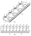
- FIG. 18 (a) and 18 (b) show another embodiment of the present invention.
- FIG. 18A and FIG. 18B are a perspective view of a plasma jet generator enlarged by arraying, and a horizontal sectional view of the gas flow widening section 23, respectively.
- This embodiment is an apparatus that can provide a wide plasma jet having a width of 200 mm by arraying four plasma processing apparatuses according to the second embodiment of the present invention.
- a single long-axis (width 210 mm, thickness 6 mm) dielectric substrate 1, four microwave input parts 13, four microstrip lines 11, and one long-axis (210 mm) ground are provided.
- Conductor 12 eight gas input ports 21, eight gas flow paths 22, four gas flow widening portions 23, one long axis (200 mm) plasma generation portion 2, and gas flow widening portion 23
- This is accomplished by providing a gas shower unit 25 provided between the plasma generating unit 2 and one long axis (200 mm) nozzle 24.
- a wide plasma jet having a width of 200 mm could be generated and maintained.
- the present invention is low in production and operation costs of the apparatus, can provide a wide range of low-temperature plasma jets not only at low pressures but also at intermediate and high pressures, and can generate high-density radicals. It can be used as a process. It can be used as a large-scale plasma generation system for material surface processes, material synthesis, environmental applications, and medical applications.
Landscapes
- Chemical & Material Sciences (AREA)
- Engineering & Computer Science (AREA)
- Physics & Mathematics (AREA)
- Plasma & Fusion (AREA)
- Materials Engineering (AREA)
- Mechanical Engineering (AREA)
- Metallurgy (AREA)
- Organic Chemistry (AREA)
- Chemical Kinetics & Catalysis (AREA)
- General Chemical & Material Sciences (AREA)
- Analytical Chemistry (AREA)
- Electromagnetism (AREA)
- Spectroscopy & Molecular Physics (AREA)
- Plasma Technology (AREA)
Abstract
Description
(1)マイクロ波電源が安い。
(2)無電極運転が可能であり、放電維持寿命が長い。
(3)インピーダンスマッチングが簡単な素子で可能。
(4)マイクロ波とプラズマのカップリング効率がよい。
(5)外部への放射損失が少なく,必要なところに電力を集中させることができる。
(6)大気圧を含め広い圧力範囲において安定な高密度プラズマが生成する。
マイクロ波入力部13は、アース導体12の孔を作り、マイクロ波コネクトを取り付けることで構成することもできる。

マイクロ波入力部13から、マイクロストリップ線路11とアース導体12との間の誘電体基板1に導入されたマイクロ波は、マイクロストリップ線路11に沿って伝搬、及び分岐される。このマイクロ波の電界は、テーパー部14のところで、マイクロストリップ線路11とアース導体12との距離が狭くなっているので徐々に強くなり、マイクロストリップ線路11の端とアース導体12の端との間で最大値になる。この集中したマイクロ波の電界が、プラズマ発生部に供給されるガスを励起し、プラズマが発生する。発生したプラズマはガスの流れと共にノズル24から吹き出る。これにより、一様な広幅のプラズマジェットを供給できる。
本発明における第2の実施の形態を示すプラズマ処理装置は、上記の第1の実施の形態を示すプラズマ処理装置において、図9に示すように、ガス流広幅化部23にガス流を一様に広げるためにガスシャワー部25が設けられた装置である。
ガスシャワー部25における上記の突起状の障害物と上記の柱は、別途に設けても良いし、誘電体基板1を加工して形成しても良い。前記の突起状の障害物と前記の柱の断面形状は、円形でも良いし、又は、三角形、四角形、等でも良い。
上記の突起状の障害物と上記の柱の形成される間隔と断面積は、気体粒子の平均自由行程(気体粒子が別の気体粒子に衝突してから次に衝突するまでの飛行距離の平均値)を考慮し、適宜に決めることができる。
次に、広幅のプラズマジェットの発生の実験について説明する。本発明における第2の実施の形態のプラズマ処理装置を用いて、大気圧空気中に発生させたプラズマジェットの写真を図11に示す。
本発明における第3の実施の形態を示すプラズマ処理装置は、上記の第1の実施の形態のプラズマ処理装置において、誘電体基板1の内部に設けられたガス入力口21と、ガス流路22と、ガス流広幅化部23と、プラズマ発生部2と、ノズル24と、が誘電体基板1の外部に設けられたプラズマ処理装置である。ガス入力口21と、ガス流路22と、ガス流広幅化部23と、プラズマ発生部2と、ノズル24と、がアース導体12と接して設けられたガス供給板27に設けられる。
本発明における第4の実施の形態を示すプラズマ処理装置は、上記の第3の実施の形態のプラズマ処理装置において、ガス流広幅化部23にガス流を一様に広げるためにガスシャワー部25が設けられた装置である。ガスシャワー部25を設けることにより、より速い流速のガス流に対しても、ガス流を一様に広幅化することができる。
本発明における第1と、第2と、第3と、第4の実施の形態に、アレイ化する技術を用いることにより、プラズマジェットを大規模化することができる。
大規模化は、一枚の長軸(幅210mm、厚み6mm)の誘電体基板1に、四つのマイクロ波入力部13と、四つのマイクロストリップ線路11と、一つの長軸(210mm)のアース導体12と、八つのガス入力口21と、八つのガス流路22と、四つのガス流広幅化部23と、一つの長軸(200mm)のプラズマ発生部2と、ガス流広幅化部23とプラズマ発生部2との間に設けられたガスシャワー部25と、一つの長軸(200mm)のノズル24とを設けることにより成し遂げられた。これにより、幅200mmの広幅プラズマジェットを発生させ維持することができた。
材料表面プロセスや、材料合成や、環境応用や、医療応用などに大規模プラズマ発生システムとして利用することができる。
2 プラズマ発生部
3 マイクロ波集中の隙間
11 マイクロストリップ線路
12 アース導体
13 マイクロ波導入部
14 テーパー部
15 マイクロストリップ線路の入力端
16 マイクロストリップ線路の分岐部
17 マイクロストリップ線路の出力側の端部
18 マイクロストリップ線路の分岐されたライン
19 マイクロストリップ線路の出力端
21 ガス入力口
22 ガス流路
23 ガス流広幅化部
24 ノズル
25 ガスシャワー部
26 ガスパイプ
27 ガス供給板
31 マイクロ波コネクト
Claims (7)
- 誘電体基板と、
前記誘電体基板の一方の端部に設けられた該誘電体基板の厚みが徐々に小さくなる形状のテーパー部と、
前記誘電体基板の表面と裏面とのうちのいずれかの面である第1の面の一方の端部から他方の端部に渡って設けられたマイクロストリップ線路と、
前記誘電体基板の前記第1の面の反対側の面である第2の面の一方の端部から他方の端部に渡って設けられたアース導体と、
前記誘電体基板の一方の端部において、前記マイクロストリップ線路と前記アース導体との間にマイクロ波を入力するためのマイクロ波入力部と、
前記誘電体基板内にガスを入力するためのガス入力口と、
前記マイクロ波入力部から入力されたマイクロ波によりプラズマを発生させるための空間であり、かつ、前記テーパー部の前記誘電体基板内に設けられた空間であるプラズマ発生部と、
前記プラズマ発生部に一様な流速を持つ広幅のガス流を供給するために前記誘電体基板内部に設けられた、ガス流が進行するに従ってガス流幅が広くなるように形成されたガス流広幅化部と、
前記ガス入力口から入力されるガスを前記ガス流広幅化部に供給するためのガス流路と、
前記プラズマ発生部に供給されるガスとマイクロ波により発生するプラズマを吐出させるためのノズルと、
を備えることを特徴とするマイクロ波プラズマ処理装置。 - 誘電体基板と、
前記誘電体基板の一方の端部に設けられた該誘電体基板の厚みが徐々に小さくなる形状のテーパー部と、
前記誘電体基板の表面と裏面とのうちのいずれかの面である第1の面の一方の端部から他方の端部に渡って設けられたマイクロストリップ線路と、
前記誘電体基板の前記第1の面の反対側の面である第2の面の一方の端部から他方の端部に渡って設けられたアース導体と、
前記誘電体基板の一方の端部において、前記マイクロストリップ線路と前記アース導体との間にマイクロ波を入力するためのマイクロ波入力部と、
前記テーパー部において、前記アース導体の端と前記マイクロストリップ線路の端とに挟まれた空間であり、前記誘電体基板の前記第2の面に形成されるマイクロ波集中の隙間と、
前記アース導体と接して、前記マイクロ波集中の隙間に一様な流速の広幅のガス流を供給するために設けられる、ガス流が進行するに従ってガス流幅が広くなるように形成されたガス流広幅化部を有するガス供給板と、
前記ガス供給板内にガスを入力するためのガス入力口と、
前記ガス供給板において、前記ガス入力口から入力されるガスを前記ガス流広幅化部に供給するためのガス流路と、
前記ガス流広幅化部から供給されるガスから、前記マイクロ波集中の隙間から放射するマイクロ波によりプラズマを発生させるための、前記ガス供給板に形成された、前記マイクロ波集中の隙間と面する空間であるプラズマ発生部と、
前記プラズマ発生部に供給するガスからマイクロ波により生成されるプラズマを吐出させるためのノズルと、
を備えることを特徴とするマイクロ波プラズマ処理装置。 - 前記ガス流広幅化部が、前記ノズルの長軸方向に沿って、一定の間隔で設けられている複数の突起状の障害物、又は柱が形成された部分であるガスシャワー部を備えている請求項1または2に記載のマイクロ波プラズマ処理装置。
- 前記マイクロストリップ線路は、
一方の端部に設けられた一つの入力端と、
前記入力端から入力されたマイクロ波を分岐する分岐部と、
前記分岐部から分かれた複数のラインと、
前記複数のラインに対応する他方の端部に設けられた複数の出力端と、
を備え、
前記他方の端部の幅を徐々に狭くすることで、インピーダンスを高め、前記プラズマ発生部におけるマイクロ波電界が強くなるようにした請求項1から3のいずれか1項に記載のマイクロ波プラズマ処理装置。 - 前記ガス流広幅化部は、
一方の端部に設けられた一つの入力端と、
前記ガス流路から入力されるガス流を分岐する分岐部と、
前記分岐部から分かれ、ガス流が進行するにつれてガス流の幅が広がるように、幅が徐々に広がるように形成された複数のラインと、
前記複数のラインから流れるガス流が一つに合流する長軸形状の空間と、
を備えた、請求項1から4のいずれか1項に記載のマイクロ波プラズマ処理装置。 - 請求項1から5のいずれか1項に記載のマイクロ波プラズマ装置を、前記誘電体基板と前記アース導体を共用して、横に並べることで、長い長軸のプラズマを発生させるように構成したマイクロ波プラズマ処理装置。
- 請求項1から6のいずれかに1項記載のマイクロ波プラズマ装置を、希ガス、又は反応性ガス、又は希ガスと反応性ガスの混合ガスを供給し、
低気圧又は中間気圧又は高気圧においてプラズマを発生させるようにしたマイクロ波プラズマ処理装置。
Priority Applications (5)
| Application Number | Priority Date | Filing Date | Title |
|---|---|---|---|
| JP2015534339A JP6153118B2 (ja) | 2013-08-30 | 2014-08-29 | マイクロ波プラズマ処理装置 |
| US14/915,482 US20160217979A1 (en) | 2013-08-30 | 2014-08-29 | Microwave plasma processing device |
| EP14839536.1A EP3041324B1 (en) | 2013-08-30 | 2014-08-29 | Microwave plasma processing device |
| KR1020167008296A KR101730094B1 (ko) | 2013-08-30 | 2014-08-29 | 마이크로파 플라스마 처리 장치 |
| CN201480048097.1A CN105684558B (zh) | 2013-08-30 | 2014-08-29 | 微波等离子体处理装置 |
Applications Claiming Priority (2)
| Application Number | Priority Date | Filing Date | Title |
|---|---|---|---|
| JP2013179286 | 2013-08-30 | ||
| JP2013-179286 | 2013-08-30 |
Publications (1)
| Publication Number | Publication Date |
|---|---|
| WO2015030191A1 true WO2015030191A1 (ja) | 2015-03-05 |
Family
ID=52586737
Family Applications (1)
| Application Number | Title | Priority Date | Filing Date |
|---|---|---|---|
| PCT/JP2014/072779 Ceased WO2015030191A1 (ja) | 2013-08-30 | 2014-08-29 | マイクロ波プラズマ処理装置 |
Country Status (6)
| Country | Link |
|---|---|
| US (1) | US20160217979A1 (ja) |
| EP (1) | EP3041324B1 (ja) |
| JP (1) | JP6153118B2 (ja) |
| KR (1) | KR101730094B1 (ja) |
| CN (1) | CN105684558B (ja) |
| WO (1) | WO2015030191A1 (ja) |
Cited By (8)
| Publication number | Priority date | Publication date | Assignee | Title |
|---|---|---|---|---|
| JP2017066506A (ja) * | 2015-10-02 | 2017-04-06 | 国立研究開発法人産業技術総合研究所 | グラフェン膜の作製方法 |
| WO2017078082A1 (ja) * | 2015-11-04 | 2017-05-11 | 国立研究開発法人産業技術総合研究所 | 窒素化合物の製造方法及び製造装置 |
| JP2020181752A (ja) * | 2019-04-26 | 2020-11-05 | ウシオ電機株式会社 | マイクロ波プラズマ発生装置 |
| JP2021044194A (ja) * | 2019-09-13 | 2021-03-18 | ウシオ電機株式会社 | マイクロ波プラズマ発生装置、及び、マイクロ波プラズマ発生装置のプラズマ放電開始方法 |
| WO2021181879A1 (ja) * | 2020-03-13 | 2021-09-16 | ウシオ電機株式会社 | 誘電体バリア式プラズマ発生装置、及び、誘電体バリア式プラズマ発生装置のプラズマ放電開始方法 |
| WO2023037583A1 (ja) * | 2021-09-10 | 2023-03-16 | ウシオ電機株式会社 | 誘電体バリア放電式プラズマ発生装置 |
| US12224474B2 (en) | 2021-12-07 | 2025-02-11 | The University Of Toledo | Power-efficient microwave plasma jet based on evanescent-mode cavity technology |
| WO2026074804A1 (ja) * | 2024-10-01 | 2026-04-09 | ウシオ電機株式会社 | プラズマ処理装置 |
Families Citing this family (12)
| Publication number | Priority date | Publication date | Assignee | Title |
|---|---|---|---|---|
| GB201410639D0 (en) | 2014-06-13 | 2014-07-30 | Fgv Cambridge Nanosystems Ltd | Apparatus and method for plasma synthesis of graphitic products including graphene |
| EP3264866A4 (en) * | 2015-02-27 | 2018-10-03 | National Institute of Advanced Industrial Science and Technology | Microwave plasma treatment apparatus |
| EP3377668B1 (en) * | 2015-11-22 | 2025-05-21 | Atmospheric Plasma Solutions, Inc. | Method and device for promoting adhesion of metallic surfaces |
| CN114269964A (zh) * | 2019-06-10 | 2022-04-01 | 斯维甘公司 | 用于衬底的气体处理的反应器 |
| KR102203878B1 (ko) * | 2019-06-11 | 2021-01-15 | 한양대학교 산학협력단 | 기판 처리 장치 및 기판 처리 방법 |
| CN114599816B (zh) * | 2019-09-09 | 2024-10-29 | 应用材料公司 | 输送反应物气体的处理系统和方法 |
| CN112941626B (zh) * | 2021-01-22 | 2022-07-22 | 北京北方华创微电子装备有限公司 | 工艺腔室的进气组件、进气装置及半导体加工设备 |
| US12018372B2 (en) * | 2021-05-11 | 2024-06-25 | Applied Materials, Inc. | Gas injector for epitaxy and CVD chamber |
| KR102844970B1 (ko) * | 2021-10-29 | 2025-08-12 | 한국전기연구원 | 마이크로파를 이용한 토양 방제장치 |
| JP7794970B2 (ja) * | 2021-11-17 | 2026-01-06 | インテグリス・インコーポレーテッド | ガスディフューザハウジング、デバイス、および関係する方法 |
| US20250183007A1 (en) * | 2021-12-07 | 2025-06-05 | The University Of Toledo | Power-efficient microwave plasma jet based on evanescent-mode cavity technology |
| US12195338B2 (en) | 2022-12-15 | 2025-01-14 | 6K Inc. | Systems, methods, and device for pyrolysis of methane in a microwave plasma for hydrogen and structured carbon powder production |
Citations (6)
| Publication number | Priority date | Publication date | Assignee | Title |
|---|---|---|---|---|
| JP2000096247A (ja) * | 1998-09-22 | 2000-04-04 | Komatsu Ltd | 表面処理装置 |
| JP2003109795A (ja) | 2001-09-27 | 2003-04-11 | Japan Science & Technology Corp | プラズマジェット発生装置 |
| JP2006107829A (ja) * | 2004-10-01 | 2006-04-20 | Univ Of Tokyo | マイクロ波励起プラズマ装置及びシステム |
| JP2007250444A (ja) * | 2006-03-17 | 2007-09-27 | Seiko Epson Corp | プラズマ装置 |
| JP2007299720A (ja) | 2006-05-01 | 2007-11-15 | Makoto Katsurai | 吹き出し形マイクロ波励起プラズマ処理装置 |
| JP2008282784A (ja) * | 2007-05-09 | 2008-11-20 | Makoto Katsurai | マイクロ波励起プラズマ処理装置 |
Family Cites Families (5)
| Publication number | Priority date | Publication date | Assignee | Title |
|---|---|---|---|---|
| FR2408972A1 (fr) * | 1977-11-15 | 1979-06-08 | Thomson Csf | Source de plasma a flux eleve, et notamment accelerateur de particules comportant un telle source |
| DE19851628B4 (de) * | 1998-11-10 | 2004-04-15 | Attila M. Dipl.-Phys. Bilgic | Streifenleitungsanordnung mit integrierten Gaszuführungen für mikrowelleninduzierte Plasmaquellen zur Anwendung in der analytischen Atomspektrometrie |
| KR100436297B1 (ko) * | 2000-03-14 | 2004-06-18 | 주성엔지니어링(주) | 반도체 소자 제조용 플라즈마 스프레이 장치 및 이를이용한 반도체 소자 제조방법 |
| DE10145131B4 (de) * | 2001-09-07 | 2004-07-08 | Pva Tepla Ag | Vorrichtung zum Erzeugen eines Aktivgasstrahls |
| US7164095B2 (en) * | 2004-07-07 | 2007-01-16 | Noritsu Koki Co., Ltd. | Microwave plasma nozzle with enhanced plume stability and heating efficiency |
-
2014
- 2014-08-29 KR KR1020167008296A patent/KR101730094B1/ko active Active
- 2014-08-29 CN CN201480048097.1A patent/CN105684558B/zh active Active
- 2014-08-29 WO PCT/JP2014/072779 patent/WO2015030191A1/ja not_active Ceased
- 2014-08-29 EP EP14839536.1A patent/EP3041324B1/en active Active
- 2014-08-29 JP JP2015534339A patent/JP6153118B2/ja active Active
- 2014-08-29 US US14/915,482 patent/US20160217979A1/en not_active Abandoned
Patent Citations (6)
| Publication number | Priority date | Publication date | Assignee | Title |
|---|---|---|---|---|
| JP2000096247A (ja) * | 1998-09-22 | 2000-04-04 | Komatsu Ltd | 表面処理装置 |
| JP2003109795A (ja) | 2001-09-27 | 2003-04-11 | Japan Science & Technology Corp | プラズマジェット発生装置 |
| JP2006107829A (ja) * | 2004-10-01 | 2006-04-20 | Univ Of Tokyo | マイクロ波励起プラズマ装置及びシステム |
| JP2007250444A (ja) * | 2006-03-17 | 2007-09-27 | Seiko Epson Corp | プラズマ装置 |
| JP2007299720A (ja) | 2006-05-01 | 2007-11-15 | Makoto Katsurai | 吹き出し形マイクロ波励起プラズマ処理装置 |
| JP2008282784A (ja) * | 2007-05-09 | 2008-11-20 | Makoto Katsurai | マイクロ波励起プラズマ処理装置 |
Non-Patent Citations (1)
| Title |
|---|
| JAEHO KIM: "Microwave-excited atmospheric-pressure plasma jets using a microstrip line", APPLIED PHYSICS LETTERS, vol. 93, 2008, pages 191505 |
Cited By (17)
| Publication number | Priority date | Publication date | Assignee | Title |
|---|---|---|---|---|
| JP2017066506A (ja) * | 2015-10-02 | 2017-04-06 | 国立研究開発法人産業技術総合研究所 | グラフェン膜の作製方法 |
| WO2017078082A1 (ja) * | 2015-11-04 | 2017-05-11 | 国立研究開発法人産業技術総合研究所 | 窒素化合物の製造方法及び製造装置 |
| JPWO2017078082A1 (ja) * | 2015-11-04 | 2018-08-30 | 国立研究開発法人産業技術総合研究所 | 窒素化合物の製造方法及び製造装置 |
| US20190153617A1 (en) * | 2015-11-04 | 2019-05-23 | National Institute Of Advanced Industrial Science And Technology | Production Method and Production Device for Nitrogen Compound |
| EP3372705A4 (en) * | 2015-11-04 | 2019-07-17 | National Institute Of Advanced Industrial Science | PROCESS AND PRODUCTION DEVICE FOR NITROGEN COMPOUND |
| JP2020181752A (ja) * | 2019-04-26 | 2020-11-05 | ウシオ電機株式会社 | マイクロ波プラズマ発生装置 |
| JP2021044194A (ja) * | 2019-09-13 | 2021-03-18 | ウシオ電機株式会社 | マイクロ波プラズマ発生装置、及び、マイクロ波プラズマ発生装置のプラズマ放電開始方法 |
| JP2021144890A (ja) * | 2020-03-13 | 2021-09-24 | ウシオ電機株式会社 | 誘電体バリア式プラズマ発生装置、及び、誘電体バリア式プラズマ発生装置のプラズマ放電開始方法 |
| WO2021181879A1 (ja) * | 2020-03-13 | 2021-09-16 | ウシオ電機株式会社 | 誘電体バリア式プラズマ発生装置、及び、誘電体バリア式プラズマ発生装置のプラズマ放電開始方法 |
| US20230100544A1 (en) * | 2020-03-13 | 2023-03-30 | Ushio Denki Kabushiki Kaisha | Dielectric barrier plasma generator and plasma discharge starting method for dielectric barrier plasma generator |
| JP7351245B2 (ja) | 2020-03-13 | 2023-09-27 | ウシオ電機株式会社 | 誘電体バリア式プラズマ発生装置、及び、誘電体バリア式プラズマ発生装置のプラズマ放電開始方法 |
| US12219688B2 (en) * | 2020-03-13 | 2025-02-04 | Ushio Denki Kabushiki Kaisha | Dielectric barrier plasma generator and plasma discharge starting method for dielectric barrier plasma generator |
| WO2023037583A1 (ja) * | 2021-09-10 | 2023-03-16 | ウシオ電機株式会社 | 誘電体バリア放電式プラズマ発生装置 |
| JP2023040527A (ja) * | 2021-09-10 | 2023-03-23 | ウシオ電機株式会社 | 誘電体バリア放電式プラズマ発生装置 |
| JP7589661B2 (ja) | 2021-09-10 | 2024-11-26 | ウシオ電機株式会社 | 誘電体バリア放電式プラズマ発生装置 |
| US12224474B2 (en) | 2021-12-07 | 2025-02-11 | The University Of Toledo | Power-efficient microwave plasma jet based on evanescent-mode cavity technology |
| WO2026074804A1 (ja) * | 2024-10-01 | 2026-04-09 | ウシオ電機株式会社 | プラズマ処理装置 |
Also Published As
| Publication number | Publication date |
|---|---|
| EP3041324A1 (en) | 2016-07-06 |
| JPWO2015030191A1 (ja) | 2017-03-02 |
| JP6153118B2 (ja) | 2017-06-28 |
| KR20160048194A (ko) | 2016-05-03 |
| CN105684558A (zh) | 2016-06-15 |
| US20160217979A1 (en) | 2016-07-28 |
| EP3041324A4 (en) | 2017-03-15 |
| KR101730094B1 (ko) | 2017-04-25 |
| CN105684558B (zh) | 2019-03-22 |
| EP3041324B1 (en) | 2020-05-13 |
Similar Documents
| Publication | Publication Date | Title |
|---|---|---|
| JP6153118B2 (ja) | マイクロ波プラズマ処理装置 | |
| US6396214B1 (en) | Device for producing a free cold plasma jet | |
| EP3264866A1 (en) | Microwave plasma treatment apparatus | |
| TWI461114B (zh) | 安定之表面波電漿源 | |
| US5648701A (en) | Electrode designs for high pressure magnetically assisted inductively coupled plasmas | |
| TWI242246B (en) | Surface wave plasma treatment apparatus using multi-slot antenna | |
| WO2007020810A1 (ja) | プラズマ処理装置 | |
| WO2005079124A1 (ja) | プラズマ発生装置 | |
| WO2010082561A1 (ja) | プラズマ生成装置及び方法 | |
| KR20150131051A (ko) | 토로이달 플라즈마 처리 장치 | |
| WO2003086032A1 (en) | Ecr plasma source and ecr plasma device | |
| JP4916776B2 (ja) | 吹き出し形マイクロ波励起プラズマ処理装置 | |
| US7159536B1 (en) | Device and method for generating a local by micro-structure electrode dis-charges with microwaves | |
| US8635972B2 (en) | Device for forming a film by deposition from a plasma | |
| US20070170996A1 (en) | Plasma generating devices having alternative ground geometry and methods for using the same | |
| TWI800643B (zh) | 利用容納之電漿的自由基來源 | |
| US20070170995A1 (en) | Plasma generating devices and methods for using the same | |
| JPH11293469A (ja) | 表面処理装置および表面処理方法 | |
| JPH08236293A (ja) | マイクロ波プラズマトーチおよびプラズマ発生方法 | |
| JP4273983B2 (ja) | 表面波励起プラズマcvd装置 | |
| CN101472384A (zh) | 大气压等离子反应器 | |
| JP2007258570A (ja) | プラズマ処理装置 | |
| JP2004200390A (ja) | プラズマ処理装置 | |
| Akram et al. | A Power-Efficient Plasma Jet Line Enabled by Dielectric Anapole Resonator Technology | |
| JP4304280B2 (ja) | プラズマ生成装置およびプラズマ処理製造方法 |
Legal Events
| Date | Code | Title | Description |
|---|---|---|---|
| 121 | Ep: the epo has been informed by wipo that ep was designated in this application |
Ref document number: 14839536 Country of ref document: EP Kind code of ref document: A1 |
|
| ENP | Entry into the national phase |
Ref document number: 2015534339 Country of ref document: JP Kind code of ref document: A |
|
| NENP | Non-entry into the national phase |
Ref country code: DE |
|
| WWE | Wipo information: entry into national phase |
Ref document number: 14915482 Country of ref document: US |
|
| REEP | Request for entry into the european phase |
Ref document number: 2014839536 Country of ref document: EP |
|
| WWE | Wipo information: entry into national phase |
Ref document number: 2014839536 Country of ref document: EP |
|
| ENP | Entry into the national phase |
Ref document number: 20167008296 Country of ref document: KR Kind code of ref document: A |