WO2015025447A1 - 半導体装置 - Google Patents
半導体装置 Download PDFInfo
- Publication number
- WO2015025447A1 WO2015025447A1 PCT/JP2014/003408 JP2014003408W WO2015025447A1 WO 2015025447 A1 WO2015025447 A1 WO 2015025447A1 JP 2014003408 W JP2014003408 W JP 2014003408W WO 2015025447 A1 WO2015025447 A1 WO 2015025447A1
- Authority
- WO
- WIPO (PCT)
- Prior art keywords
- semiconductor
- semiconductor device
- fixed
- support plate
- metal block
- Prior art date
- Legal status (The legal status is an assumption and is not a legal conclusion. Google has not performed a legal analysis and makes no representation as to the accuracy of the status listed.)
- Ceased
Links
Images

Classifications
-
- H—ELECTRICITY
- H10—SEMICONDUCTOR DEVICES; ELECTRIC SOLID-STATE DEVICES NOT OTHERWISE PROVIDED FOR
- H10W—GENERIC PACKAGES, INTERCONNECTIONS, CONNECTORS OR OTHER CONSTRUCTIONAL DETAILS OF DEVICES COVERED BY CLASS H10
- H10W76/00—Containers; Fillings or auxiliary members therefor; Seals
- H10W76/10—Containers or parts thereof
- H10W76/12—Containers or parts thereof characterised by their shape
- H10W76/15—Containers comprising an insulating or insulated base
-
- H—ELECTRICITY
- H10—SEMICONDUCTOR DEVICES; ELECTRIC SOLID-STATE DEVICES NOT OTHERWISE PROVIDED FOR
- H10W—GENERIC PACKAGES, INTERCONNECTIONS, CONNECTORS OR OTHER CONSTRUCTIONAL DETAILS OF DEVICES COVERED BY CLASS H10
- H10W40/00—Arrangements for thermal protection or thermal control
- H10W40/20—Arrangements for cooling
- H10W40/22—Arrangements for cooling characterised by their shape, e.g. having conical or cylindrical projections
-
- H—ELECTRICITY
- H10—SEMICONDUCTOR DEVICES; ELECTRIC SOLID-STATE DEVICES NOT OTHERWISE PROVIDED FOR
- H10W—GENERIC PACKAGES, INTERCONNECTIONS, CONNECTORS OR OTHER CONSTRUCTIONAL DETAILS OF DEVICES COVERED BY CLASS H10
- H10W40/00—Arrangements for thermal protection or thermal control
- H10W40/60—Securing means for detachable heating or cooling arrangements, e.g. clamps
- H10W40/611—Bolts or screws
-
- H—ELECTRICITY
- H10—SEMICONDUCTOR DEVICES; ELECTRIC SOLID-STATE DEVICES NOT OTHERWISE PROVIDED FOR
- H10W—GENERIC PACKAGES, INTERCONNECTIONS, CONNECTORS OR OTHER CONSTRUCTIONAL DETAILS OF DEVICES COVERED BY CLASS H10
- H10W70/00—Package substrates; Interposers; Redistribution layers [RDL]
- H10W70/60—Insulating or insulated package substrates; Interposers; Redistribution layers
- H10W70/62—Insulating or insulated package substrates; Interposers; Redistribution layers characterised by their interconnections
- H10W70/65—Shapes or dispositions of interconnections
-
- H—ELECTRICITY
- H10—SEMICONDUCTOR DEVICES; ELECTRIC SOLID-STATE DEVICES NOT OTHERWISE PROVIDED FOR
- H10W—GENERIC PACKAGES, INTERCONNECTIONS, CONNECTORS OR OTHER CONSTRUCTIONAL DETAILS OF DEVICES COVERED BY CLASS H10
- H10W74/00—Encapsulations, e.g. protective coatings
- H10W74/10—Encapsulations, e.g. protective coatings characterised by their shape or disposition
- H10W74/111—Encapsulations, e.g. protective coatings characterised by their shape or disposition the semiconductor body being completely enclosed
- H10W74/114—Encapsulations, e.g. protective coatings characterised by their shape or disposition the semiconductor body being completely enclosed by a substrate and the encapsulations
-
- H—ELECTRICITY
- H10—SEMICONDUCTOR DEVICES; ELECTRIC SOLID-STATE DEVICES NOT OTHERWISE PROVIDED FOR
- H10W—GENERIC PACKAGES, INTERCONNECTIONS, CONNECTORS OR OTHER CONSTRUCTIONAL DETAILS OF DEVICES COVERED BY CLASS H10
- H10W76/00—Containers; Fillings or auxiliary members therefor; Seals
- H10W76/40—Fillings or auxiliary members in containers, e.g. centering rings
-
- H—ELECTRICITY
- H10—SEMICONDUCTOR DEVICES; ELECTRIC SOLID-STATE DEVICES NOT OTHERWISE PROVIDED FOR
- H10W—GENERIC PACKAGES, INTERCONNECTIONS, CONNECTORS OR OTHER CONSTRUCTIONAL DETAILS OF DEVICES COVERED BY CLASS H10
- H10W90/00—Package configurations
-
- H—ELECTRICITY
- H10—SEMICONDUCTOR DEVICES; ELECTRIC SOLID-STATE DEVICES NOT OTHERWISE PROVIDED FOR
- H10W—GENERIC PACKAGES, INTERCONNECTIONS, CONNECTORS OR OTHER CONSTRUCTIONAL DETAILS OF DEVICES COVERED BY CLASS H10
- H10W40/00—Arrangements for thermal protection or thermal control
- H10W40/20—Arrangements for cooling
- H10W40/231—Arrangements for cooling characterised by their places of attachment or cooling paths
-
- H—ELECTRICITY
- H10—SEMICONDUCTOR DEVICES; ELECTRIC SOLID-STATE DEVICES NOT OTHERWISE PROVIDED FOR
- H10W—GENERIC PACKAGES, INTERCONNECTIONS, CONNECTORS OR OTHER CONSTRUCTIONAL DETAILS OF DEVICES COVERED BY CLASS H10
- H10W40/00—Arrangements for thermal protection or thermal control
- H10W40/20—Arrangements for cooling
- H10W40/231—Arrangements for cooling characterised by their places of attachment or cooling paths
- H10W40/237—Arrangements for cooling characterised by their places of attachment or cooling paths attached to additional arrangements for cooling
-
- H—ELECTRICITY
- H10—SEMICONDUCTOR DEVICES; ELECTRIC SOLID-STATE DEVICES NOT OTHERWISE PROVIDED FOR
- H10W—GENERIC PACKAGES, INTERCONNECTIONS, CONNECTORS OR OTHER CONSTRUCTIONAL DETAILS OF DEVICES COVERED BY CLASS H10
- H10W40/00—Arrangements for thermal protection or thermal control
- H10W40/20—Arrangements for cooling
- H10W40/25—Arrangements for cooling characterised by their materials
- H10W40/255—Arrangements for cooling characterised by their materials having a laminate or multilayered structure, e.g. direct bond copper [DBC] ceramic substrates
-
- H—ELECTRICITY
- H10—SEMICONDUCTOR DEVICES; ELECTRIC SOLID-STATE DEVICES NOT OTHERWISE PROVIDED FOR
- H10W—GENERIC PACKAGES, INTERCONNECTIONS, CONNECTORS OR OTHER CONSTRUCTIONAL DETAILS OF DEVICES COVERED BY CLASS H10
- H10W40/00—Arrangements for thermal protection or thermal control
- H10W40/60—Securing means for detachable heating or cooling arrangements, e.g. clamps
-
- H—ELECTRICITY
- H10—SEMICONDUCTOR DEVICES; ELECTRIC SOLID-STATE DEVICES NOT OTHERWISE PROVIDED FOR
- H10W—GENERIC PACKAGES, INTERCONNECTIONS, CONNECTORS OR OTHER CONSTRUCTIONAL DETAILS OF DEVICES COVERED BY CLASS H10
- H10W70/00—Package substrates; Interposers; Redistribution layers [RDL]
- H10W70/60—Insulating or insulated package substrates; Interposers; Redistribution layers
- H10W70/62—Insulating or insulated package substrates; Interposers; Redistribution layers characterised by their interconnections
- H10W70/65—Shapes or dispositions of interconnections
- H10W70/658—Shapes or dispositions of interconnections for devices provided for in groups H10D8/00 - H10D48/00
-
- H—ELECTRICITY
- H10—SEMICONDUCTOR DEVICES; ELECTRIC SOLID-STATE DEVICES NOT OTHERWISE PROVIDED FOR
- H10W—GENERIC PACKAGES, INTERCONNECTIONS, CONNECTORS OR OTHER CONSTRUCTIONAL DETAILS OF DEVICES COVERED BY CLASS H10
- H10W72/00—Interconnections or connectors in packages
- H10W72/071—Connecting or disconnecting
- H10W72/075—Connecting or disconnecting of bond wires
- H10W72/07551—Connecting or disconnecting of bond wires characterised by changes in properties of the bond wires during the connecting
-
- H—ELECTRICITY
- H10—SEMICONDUCTOR DEVICES; ELECTRIC SOLID-STATE DEVICES NOT OTHERWISE PROVIDED FOR
- H10W—GENERIC PACKAGES, INTERCONNECTIONS, CONNECTORS OR OTHER CONSTRUCTIONAL DETAILS OF DEVICES COVERED BY CLASS H10
- H10W72/00—Interconnections or connectors in packages
- H10W72/20—Bump connectors, e.g. solder bumps or copper pillars; Dummy bumps; Thermal bumps
- H10W72/221—Structures or relative sizes
-
- H—ELECTRICITY
- H10—SEMICONDUCTOR DEVICES; ELECTRIC SOLID-STATE DEVICES NOT OTHERWISE PROVIDED FOR
- H10W—GENERIC PACKAGES, INTERCONNECTIONS, CONNECTORS OR OTHER CONSTRUCTIONAL DETAILS OF DEVICES COVERED BY CLASS H10
- H10W72/00—Interconnections or connectors in packages
- H10W72/20—Bump connectors, e.g. solder bumps or copper pillars; Dummy bumps; Thermal bumps
- H10W72/231—Shapes
- H10W72/234—Cross-sectional shape, i.e. in side view
-
- H—ELECTRICITY
- H10—SEMICONDUCTOR DEVICES; ELECTRIC SOLID-STATE DEVICES NOT OTHERWISE PROVIDED FOR
- H10W—GENERIC PACKAGES, INTERCONNECTIONS, CONNECTORS OR OTHER CONSTRUCTIONAL DETAILS OF DEVICES COVERED BY CLASS H10
- H10W72/00—Interconnections or connectors in packages
- H10W72/20—Bump connectors, e.g. solder bumps or copper pillars; Dummy bumps; Thermal bumps
- H10W72/241—Dispositions, e.g. layouts
- H10W72/242—Dispositions, e.g. layouts relative to the surface, e.g. recessed, protruding
-
- H—ELECTRICITY
- H10—SEMICONDUCTOR DEVICES; ELECTRIC SOLID-STATE DEVICES NOT OTHERWISE PROVIDED FOR
- H10W—GENERIC PACKAGES, INTERCONNECTIONS, CONNECTORS OR OTHER CONSTRUCTIONAL DETAILS OF DEVICES COVERED BY CLASS H10
- H10W72/00—Interconnections or connectors in packages
- H10W72/50—Bond wires
-
- H—ELECTRICITY
- H10—SEMICONDUCTOR DEVICES; ELECTRIC SOLID-STATE DEVICES NOT OTHERWISE PROVIDED FOR
- H10W—GENERIC PACKAGES, INTERCONNECTIONS, CONNECTORS OR OTHER CONSTRUCTIONAL DETAILS OF DEVICES COVERED BY CLASS H10
- H10W90/00—Package configurations
- H10W90/401—Package configurations characterised by multiple insulating or insulated package substrates, interposers or RDLs
-
- H—ELECTRICITY
- H10—SEMICONDUCTOR DEVICES; ELECTRIC SOLID-STATE DEVICES NOT OTHERWISE PROVIDED FOR
- H10W—GENERIC PACKAGES, INTERCONNECTIONS, CONNECTORS OR OTHER CONSTRUCTIONAL DETAILS OF DEVICES COVERED BY CLASS H10
- H10W90/00—Package configurations
- H10W90/701—Package configurations characterised by the relative positions of pads or connectors relative to package parts
-
- H—ELECTRICITY
- H10—SEMICONDUCTOR DEVICES; ELECTRIC SOLID-STATE DEVICES NOT OTHERWISE PROVIDED FOR
- H10W—GENERIC PACKAGES, INTERCONNECTIONS, CONNECTORS OR OTHER CONSTRUCTIONAL DETAILS OF DEVICES COVERED BY CLASS H10
- H10W90/00—Package configurations
- H10W90/701—Package configurations characterised by the relative positions of pads or connectors relative to package parts
- H10W90/721—Package configurations characterised by the relative positions of pads or connectors relative to package parts of bump connectors
- H10W90/724—Package configurations characterised by the relative positions of pads or connectors relative to package parts of bump connectors between a chip and a stacked insulating package substrate, interposer or RDL
-
- H—ELECTRICITY
- H10—SEMICONDUCTOR DEVICES; ELECTRIC SOLID-STATE DEVICES NOT OTHERWISE PROVIDED FOR
- H10W—GENERIC PACKAGES, INTERCONNECTIONS, CONNECTORS OR OTHER CONSTRUCTIONAL DETAILS OF DEVICES COVERED BY CLASS H10
- H10W90/00—Package configurations
- H10W90/701—Package configurations characterised by the relative positions of pads or connectors relative to package parts
- H10W90/751—Package configurations characterised by the relative positions of pads or connectors relative to package parts of bond wires
- H10W90/754—Package configurations characterised by the relative positions of pads or connectors relative to package parts of bond wires between a chip and a stacked insulating package substrate, interposer or RDL
Definitions
- the present invention relates to a semiconductor device, and more particularly to a power semiconductor module on which a power semiconductor chip is mounted.
- a semiconductor device In an inverter device, an uninterruptible power supply device, a machine tool, an industrial robot, and the like, a semiconductor device (power semiconductor module) is used independently of the main body device.
- a conventional power semiconductor module for example, one described in Patent Document 1 is known.
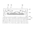
- the configuration of a conventional power semiconductor module is shown in FIG.
- the power semiconductor module includes a heat sink 101, an insulating substrate 103, a semiconductor chip 102, a resin case 104, and the like.
- the heat sink 101 includes a base 101a and a cooling fin 101b having high thermal conductivity.
- the insulating substrate 103 on which the semiconductor chip 102 is mounted is fixed on the base 101a. Further, the semiconductor chip 102 and the insulating substrate 103 are surrounded by a resin case 104.
- Patent Document 2 describes a power semiconductor module in which a plurality of semiconductor units and a bolt fastening unit are integrated with an elastic adhesive and can be fixed to a heat sink with the bolt fastening unit.
- the power semiconductor module described in Patent Document 2 can be prepared with various rated power semiconductor modules by combining a plurality of single rated semiconductor units.
- the central semiconductor unit is arranged apart from the bolting unit.
- each semiconductor unit and the bolting unit are fixed with an elastic adhesive, the pressure contact force to the heat sink is not easily transmitted to the semiconductor unit separated from the bolting unit. Therefore, there exists a subject that the cooling efficiency of the semiconductor chip mounted in the said semiconductor unit reduces. Therefore, the present invention has been made paying attention to the problems of the conventional example described above, and by sharing the basic structure constituting the semiconductor device, it is possible to improve the production efficiency and ensure sufficient cooling efficiency.
- An object is to provide a semiconductor device.
- a semiconductor device has a first surface, a second surface located on the opposite side of the first surface, and a support having a through hole penetrating from the first surface to the second surface.
- a semiconductor unit having a plate, a semiconductor chip, an external electrode, and a protruding metal block is fixed to the first surface, and the metal block penetrates to the second surface through a through hole.
- the present invention it is possible to improve the production efficiency by sharing the basic configuration of the semiconductor device, and to provide a semiconductor device capable of ensuring sufficient cooling efficiency.
- FIG. 1 is a cross-sectional view showing an embodiment of a semiconductor device according to a first embodiment of the present invention. It is an expanded sectional view which shows the semiconductor unit of FIG. It is sectional drawing which shows one Embodiment of the semiconductor device which concerns on the 2nd Embodiment of this invention. It is sectional drawing which shows a prior art example.
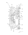
- FIG. 1 is a cross-sectional view showing an overall configuration of a first embodiment of a semiconductor device according to the present invention
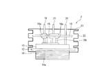
- FIG. 2 is an enlarged cross-sectional view showing a semiconductor unit of FIG.
- a power semiconductor module 1 as a semiconductor device according to the present invention includes a semiconductor unit 2 and a support plate 3. The support plate 3 is fixed to the heat sink 4.
- the semiconductor unit 2 includes a semiconductor chip 15 and a metal block 14.
- the semiconductor unit 2 also includes a circuit board 13, an insulating board 12, external electrodes 19, 20, 21, and a sealing resin 22.
- the semiconductor chip 15 is a power semiconductor element such as an insulated gate bipolar transistor (IGBT), a power MOSFET, or a free wheel diode (FWD).
- the metal block 14 has a columnar shape and protrudes outward from the sealing resin 22. And the thickness of this protrusion part is thicker than the thickness of the support plate 3, and it equips the outer peripheral surface with the external thread part 14a.
- the male screw portion 14a can be formed by precision machining.
- the support plate 3 has a first surface 3a, a second surface 3b located on the opposite side of the first surface 3a, and a through hole 16 penetrating from the first surface 3a to the second surface 3b. Further, the inner peripheral surface of the through hole 16 has a female screw portion 16a corresponding to the male screw portion 14a. The female thread portion 16a can be formed by precision machining. Furthermore, the support plate 3 has a mounting hole 17 on the outer edge.
- the support plate 3 is made of a single material such as Cu or Al having a high thermal conductivity, W or Mo having a low linear expansion coefficient, for example. Alternatively, the support plate 3 is composed of a composite material such as Cu—C, Al—C, Al—SiC, Cu—Mo, Cu, Cu—W, and Si—SiC that has high thermal conductivity and low linear expansion coefficient. Is done.
- a wiring board 18 having a metal layer 18a is disposed opposite to the circuit board 13.
- One end of a conductive post 18b is electrically and mechanically connected to the metal layer 18a of the wiring board 18.
- the other end of the conductive post 18 b is electrically and mechanically connected to the front surface electrode of the semiconductor chip 15 or the circuit board 13. That is, the internal wiring of the semiconductor unit 2 is performed by the wiring substrate 18 and the conductive posts 18b, not by the conventional bonding wires.
- the connection terminals 19, 20, and 21 are electrically and mechanically connected to the circuit board 13 and the metal layer 18 b of the wiring board 18.
- the insulating plate 12, the circuit board 13, the semiconductor chip 15, and the wiring board 18 are covered with a sealing resin 22 that is a thermosetting resin such as an epoxy resin. Further, the sealing resin 22 has unevenness on its side surface for extending the creepage distance. Furthermore, as shown in FIG. 2, the sealing resin 22 preferably includes a protective film 23 made of an inorganic material such as Al 2 O 3 , AlN, Si 3 N 4 , SiO 2 , or BN, as shown in FIG. . The metal block 14 and the connection terminals 19 to 21 protrude outward from the sealing resin 22. Then, the two semiconductor units 2 having the above configuration are screwed into the female screw portion 16a of the support plate 3 from the first surface 3a side using the male screw portion 14a of the metal block 14.
- a sealing resin 22 that is a thermosetting resin such as an epoxy resin.
- the sealing resin 22 has unevenness on its side surface for extending the creepage distance.
- the sealing resin 22 preferably includes a protective film 23 made of an inorganic material such
- the bottom surface of the sealing resin 22 is brought into contact with the upper surface of the support plate 3 and fixed to the support plate 3.
- the end surface of the metal block 14 is projected from the second surface 3 b of the support plate 3 by a predetermined distance.
- an external terminal 25 is provided which electrically connects between the connection terminals 19 to 21 protruding from the two semiconductor units 2 to constitute a desired circuit.
- the external terminal 25 includes, for example, flat-shaped bus bars 26, 27, and 28, and terminal portions 29, 30 and 31 connected to these bus bars. Then, the semiconductor unit 2 and the external terminals 25 are covered with a casing 32 made of insulating resin or the like, and the terminal portions 29 to 31 are protruded outward from the casing 32.
- the semiconductor device 1 which is a 2 in 1 power semiconductor module which is one embodiment of the present invention is configured.
- the semiconductor device 1 When the semiconductor device 1 having the above configuration is used, the semiconductor device 1 is fixed to the fixing surface 4 a of the heat sink 4.
- the mounting hole 17 of the support plate 3 and the female screw part 4b of the heat sink 4 are aligned, and a set screw 33 is inserted into the mounting hole 17 and screwed into the female screw part 4b.
- the metal block 14 and the fixed surface 4a are in direct contact with each other.
- the semiconductor unit 2 having the semiconductor chip 15 and the protruding metal block 14 is fixed to the support plate 3, and the support plate 3 is fixed to the heat sink 4 by the set screw 33.
- a plurality of semiconductor units 2 with a single rating can be combined with the support plate 3, and power semiconductor modules with various ratings can be prepared.
- the metal block 14 of the semiconductor unit 2 is in direct contact with the heat sink 4. For this reason, the heat generated from the semiconductor chip 15 can be radiated directly to the heat sink 4 via the metal block 14, and the cooling efficiency can be improved.
- the plurality of semiconductor units 2 are fixed to the support plate 3 by screwing, the amount of protrusion from the second surface 3b can be accurately adjusted. Therefore, the contact state between the fixed surface 4a of the heat sink 4 and the metal block 14 of each semiconductor unit 2 can be favorably maintained. Moreover, since the semiconductor unit 2 can be pressed against the heat sink 4 not via the elastic adhesive as described in Patent Document 2 but via the support plate 3, sufficient cooling efficiency can be achieved even in the central semiconductor unit. Can be secured. Further, since the semiconductor unit 2 can be fixed to the support plate 3 only by screwing, the manufacturing cost can be reduced.
- the insulating substrate 103 on which the semiconductor chip 102 is mounted is directly joined to the base 101a of the heat sink 101 by soldering or the like as in the conventional example described above, a jig for positioning is required.
- the flatness can not be joined while ensuring.
- the metal block 14 of the semiconductor unit 2 is screwed to the support plate 3, so that the amount of protrusion of the metal block 14 from the support plate 3 is achieved by performing high-precision machining. Can be accurately adjusted, and the flatness of the end faces of the metal blocks 14 of the plurality of semiconductor units 2 can be accurately ensured.
- FIG. 3 is a cross-sectional view showing the overall configuration of the second embodiment of the semiconductor device according to the present invention.
- the power semiconductor module 50 which is an aspect of the semiconductor device according to the present invention further includes a heat transfer plate 40 and a bolt 41.
- the heat transfer plate 40 has a first surface 40a and a second surface 40b located on the opposite side. As for the heat exchanger plate 40, the 2nd surface 40b is being fixed to the terminal surface 32a of the housing
- terminal portions 29 to 31 of the external terminal 25 protruding from the terminal surface 32a of the housing 32 are inserted into the terminal holes 41 provided on the second surface 40b of the heat transfer plate 40 in a state of being bent in an L shape. is doing. Further, the terminal portions 29 to 31 are fixed by using bolts 42 inserted from the first surface 40a and nuts 43 inserted from the second main surface. At this time, it is preferable to form the recessed part 50 which engages
- casing 32 can be improved. Further, it is possible to fix a further external device to the semiconductor device 50 by using the fastening hole 44 provided in the first surface 40 a of the heat transfer plate 40. This is because the heat transfer plate 40 is firmly fixed to the housing 32 by using two means of the terminal portions 29 to 31 fixed by an adhesive, bolts 42 and nuts 43.
- the present invention is not limited to this.
- the end surface of the metal block 14 and the second surface 3b of the support plate 3 may be in the same plane.
- the present invention is not limited to the above-described configuration, and as long as the protruding metal block 14 is provided, electrical connection may be performed using a bonding wire as in the conventional example.
- the semiconductor unit 2 is an insulating semiconductor unit including the insulating plate 12
- the present invention is not limited to this.
- a non-insulating semiconductor unit that does not have the insulating plate 12 can be fixed to the support plate 3 in the same manner as described above.
- the said embodiment demonstrated the case where the two semiconductor units 2 were fixed to the support plate 3, it is not limited to this. According to the number of semiconductor units required for a desired rating, the through hole 16 having the female screw portion 16a may be formed in the support plate 3.
- the semiconductor unit 2 has one semiconductor chip 15 has been described.
- the present invention is not limited to this, and two or more semiconductor chips may be fixed to the circuit board 13.
- the said embodiment demonstrated the case where the support plate 3 was fixed to the heat sink 4 with the set screw 33, it is not limited to this,
- the male screw part fixed to the heat sink 4 is inserted in the support plate 3, and
- the nut may protrude from the first surface 3a and a nut may be screwed into the male screw portion.
- the semiconductor device of the present invention has been specifically described with reference to the drawings and embodiments, the semiconductor device of the present invention is not limited to the description of the embodiments and drawings, and does not depart from the spirit of the present invention. Many variations in range are possible.
Landscapes
- Cooling Or The Like Of Semiconductors Or Solid State Devices (AREA)
- Engineering & Computer Science (AREA)
- Microelectronics & Electronic Packaging (AREA)
- Physics & Mathematics (AREA)
- Geometry (AREA)
Abstract
Description
従来のパワー半導体モジュールとしては、例えば特許文献1に記載されているものが知られている。従来のパワー半導体モジュールの構成を図4に示す。このパワー半導体モジュールは、ヒートシンク101と、絶縁基板103と、半導体チップ102と、樹脂ケース104などで構成されている。ヒートシンク101は、熱伝導性の高いベース101aおよび冷却フィン101bで構成される。そして、ベース101a上に半導体チップ102を実装した絶縁基板103が固着されている。また、半導体チップ102および絶縁基板103が樹脂ケース104で囲まれている。さらに、半導体チップ102のおもて面電極にはボンディングワイヤ105が接合され、絶縁基板103の回路板106と電気的に接続されている。また、樹脂ケース104の上端を蓋107で覆い、蓋107を貫通して上方に突出する外部端子108が回路板106上に配置されている。
また、特許文献2には、複数の半導体ユニットとボルト締めユニットを弾性接着剤で一体化し、ボルト締めユニットでヒートシンクに固定可能としたパワー半導体モジュールが記載されている。
特許文献1に記載のパワー半導体モジュールでは、半導体チップ102、絶縁基板103、樹脂ケース104、蓋体107および端子108を各定格に応じてそれぞれ用意する必要がある。
さらに、製造に必要な治工具もそれぞれの定格で必要となるため、製造コストの低減が困難という課題がある。
そこで、本発明では、上記従来例の問題点に着目してなされたものであり、半導体装置を構成する基本構造を共通化して、生産効率の向上を図るとともに、十分な冷却効率を確保可能な半導体装置を提供することを目的としている。
なお、本出願の記載に用いられている「電気的かつ機械的に接続されている」という用語は、対象物同士が直接接合により接続されている場合に限られず、ハンダや金属焼結材などの導電性の接合材を介して対象物同士が接続されている場合も含むものとする。
図1は本発明に係る半導体装置の第1の実施形態の全体構成を示す断面図、図2は図1の半導体ユニットを示す拡大断面図である。
本発明に係る半導体装置としてのパワー半導体モジュール1は、半導体ユニット2と、支持板3を備えている。そして、支持板3がヒートシンク4に固定されている。
半導体チップ15は、例えば絶縁ゲートバイポーラトランジスタ(IGBT)やパワーMOSFET、還流ダイオード(FWD)等のパワー半導体素子である。
金属ブロック14は、円柱状であり、封止樹脂22から外方に突出している。そして、この突出部分の厚さは、支持板3の厚さより厚く、またその外周面に雄ねじ部14aを備えている。雄ねじ部14aは、精密機械加工により形成できる。
そして、上記構成を有する2つの半導体ユニット2を、金属ブロック14の雄ねじ部14aを用いて、支持板3の雌ねじ部16aに第1面3a側から螺合させる。そして、封止樹脂22の底面を支持板3の上面に接触させて、支持板3に固定する。またその際、金属ブロック14の端面は、支持板3の第2面3bより所定の距離突出させる。
そして、半導体ユニット2や外部端子25を、絶縁樹脂などで構成される筐体32で覆い、端子部29~31を筐体32から外方に突出させる。これにより、本発明の一態様である2in1のパワー半導体モジュールとなる半導体装置1が構成される。
このように、上記実施形態によると、半導体チップ15と、突出した金属ブロック14を有する半導体ユニット2を支持板3に固定し、この支持板3をヒートシンク4に止めねじ33によって固定している。これにより、一つの定格の半導体ユニット2を支持板3で複数組み合わせることができ、さまざまな定格のパワー半導体モジュールを用意することができる。また、半導体ユニット2の金属ブロック14が直接ヒートシンク4に接触している。このため、半導体チップ15からの発熱を、金属ブロック14を介して直接ヒートシンク4に放熱することができ、冷却効率を改善することができる。
また、半導体ユニット2の支持板3への固定を螺合させるだけで可能なため、製造コストを低減することができる。
本発明に係る半導体装置の一態様であるパワー半導体モジュール50は、伝熱板40と、ボルト41をさらに備えている。
伝熱板40は、第1面40aとその反対側に位置する第2面40bとを有している。伝熱板40は、第2面40bが筐体32の端子面32aに、接着材などを用いて固定されている。また、筐体32の端子面32aから突出している外部端子25の端子部29~31を、L字状に折り曲げた状態で伝熱板40の第2面40bに設けられた端子孔41に挿通している。さらに、端子部29~31は第1面40aから挿通されたボルト42および第2主面から挿通されたナット43を用いて固定している。このとき、筐体32の端子面32aにナット43を嵌め込んで回り止めを行う凹部50を形成することが好ましい。
なお、上記実施形態においては、半導体ユニット2の金属ブロック14を支持板3の第2面3bから突出させる場合について説明したが、これに限定されるものではない。例えば、金属ブロック14の端面と、支持板3の第2面3bとが同一平面となるようにしてもよい。
また、上記実施形態においては、半導体ユニット2が絶縁板12を備えた絶縁型の半導体ユニットである場合について説明したが、これに限定されるものではない。例えば、絶縁板12を有さない非絶縁型の半導体ユニットであっても、上記と同様に支持板3に固定することができる。
また、上記実施形態では、支持板3に2つの半導体ユニット2を固定する場合について説明したが、これに限定されるものではない。所望の定格に必要な半導体ユニットの数に応じて、支持板3に雌ねじ部16aを有する貫通孔16を形成すればよいものである。
また、上記実施形態では、支持板3をヒートシンク4に止めねじ33によって固定する場合について説明したが、これに限定されるものではなく、ヒートシンク4に固定した雄ねじ部を支持板3に挿通して、第1面3aより突出させ、この雄ねじ部にナットを螺合させるようにしてもよい。要は、支持板3に支持した金属ブロックがヒートシンク4に接触した状態で固定されればよく、任意の固定手段を適用することができる。
以上、本発明の半導体装置を図面及び実施形態を用いて具体的に説明したが、本発明の半導体装置は、実施形態及び図面の記載に限定されるものではなく、本発明の趣旨を逸脱しない範囲で幾多の変形が可能である。
2 半導体ユニット
3 支持板
3a 第1面
3b 第2面
4 ヒートシンク
12 絶縁板
13 回路板
14 金属ブロック
14a 雄ねじ部
15 半導体チップ
16 貫通孔
16a 雌ねじ部
17 取付孔
18 配線基板
19~21 接続端子
22 封止樹脂
23 保護膜
25 外部端子
29~31 端子部
32 筐体
40 伝熱板
41 ボルト
42 ナット
Claims (12)
- 第1面と、前記第1面の反対側に位置する第2面と、前記第1面から前記第2面まで貫通する貫通孔を有する支持板と、
半導体チップと、突出した金属ブロックを有し、前記第1面に固定され、前記金属ブロックは前記貫通孔を通じて前記第2面まで貫通している半導体ユニットと、
を備えた半導体装置。 - 前記半導体ユニットは、絶縁板、および前記絶縁板のおもて面に固定された回路板をさらに有し、
前記半導体チップは前記回路板に固定され、
前記金属ブロックは前記絶縁板の裏面に固定された請求項1記載の半導体装置。 - 前記金属ブロックが、前記第2面から突出している請求項1に記載の半導体装置。
- 前記金属ブロックは雄ねじ部を備え、
前記貫通孔は雌ねじ部を備え、
前記半導体ユニットは、前記雄ねじ部と前記雌ねじ部との螺合により、前記第1面に固定されている請求項1に記載の半導体装置。 - 前記支持板は複数の前記貫通孔を有し、
前記複数の貫通孔に、複数の前記半導体ユニットがそれぞれ固定されている請求項1に記載の半導体装置。 - 前記半導体ユニットは外部電極をさらに有し、
複数の前記半導体ユニットが有する前記外部電極をそれぞれ接続する外部端子をさらに備えた請求項5に記載の半導体装置。 - 複数の前記半導体ユニットおよび前記外部端子を覆う筐体と、
前記筐体に固定される伝熱板と、
をさらに備えた請求項6記載の半導体装置。 - 前記伝熱板は、前記外部端子を挿入する端子孔を有する請求項7記載の半導体装置。
- 前記半導体ユニットは、前記半導体チップを覆う封止樹脂を有する請求項1に記載の半導体装置。
- 前記支持板は、Cu、Al、Mo、W、Cu-C、Al-C、Al-SiC、Cu-Mo、Si-SiCの何れか1つで構成されている請求項1に記載の半導体装置。
- 前記半導体ユニットは、側面に凹凸を有する請求項1に記載の半導体装置。
- 前記半導体ユニットは、表面にAl2O3、AlN、Si3N4、Si02、BNの何れか1つで構成される保護膜を有する請求項1に記載の半導体装置。
Priority Applications (3)
| Application Number | Priority Date | Filing Date | Title |
|---|---|---|---|
| JP2015532684A JP6160698B2 (ja) | 2013-08-23 | 2014-06-25 | 半導体装置 |
| CN201480015666.2A CN105051898B (zh) | 2013-08-23 | 2014-06-25 | 半导体装置 |
| US14/851,748 US9842786B2 (en) | 2013-08-23 | 2015-09-11 | Semiconductor device |
Applications Claiming Priority (2)
| Application Number | Priority Date | Filing Date | Title |
|---|---|---|---|
| JP2013-173487 | 2013-08-23 | ||
| JP2013173487 | 2013-08-23 |
Related Child Applications (1)
| Application Number | Title | Priority Date | Filing Date |
|---|---|---|---|
| US14/851,748 Continuation US9842786B2 (en) | 2013-08-23 | 2015-09-11 | Semiconductor device |
Publications (1)
| Publication Number | Publication Date |
|---|---|
| WO2015025447A1 true WO2015025447A1 (ja) | 2015-02-26 |
Family
ID=52483247
Family Applications (1)
| Application Number | Title | Priority Date | Filing Date |
|---|---|---|---|
| PCT/JP2014/003408 Ceased WO2015025447A1 (ja) | 2013-08-23 | 2014-06-25 | 半導体装置 |
Country Status (4)
| Country | Link |
|---|---|
| US (1) | US9842786B2 (ja) |
| JP (1) | JP6160698B2 (ja) |
| CN (1) | CN105051898B (ja) |
| WO (1) | WO2015025447A1 (ja) |
Cited By (3)
| Publication number | Priority date | Publication date | Assignee | Title |
|---|---|---|---|---|
| CN106340499A (zh) * | 2015-07-08 | 2017-01-18 | 三菱电机株式会社 | 半导体模块 |
| US10658343B2 (en) | 2016-12-16 | 2020-05-19 | Fuji Electric Co., Ltd. | Semiconductor module including pressure contact adjustment screws |
| JP2022191866A (ja) * | 2021-06-16 | 2022-12-28 | 富士電機株式会社 | 半導体装置 |
Families Citing this family (4)
| Publication number | Priority date | Publication date | Assignee | Title |
|---|---|---|---|---|
| JP2016009745A (ja) * | 2014-06-24 | 2016-01-18 | 富士通株式会社 | 電子部品、電子部品の製造方法及び電子装置 |
| JP7025948B2 (ja) * | 2018-02-13 | 2022-02-25 | ローム株式会社 | 半導体装置および半導体装置の製造方法 |
| CN109637988A (zh) * | 2019-01-29 | 2019-04-16 | 西安微电子技术研究所 | 一种低热阻压力可控式散热盒体结构 |
| JP7309396B2 (ja) * | 2019-03-18 | 2023-07-18 | 株式会社東芝 | 半導体装置 |
Citations (8)
| Publication number | Priority date | Publication date | Assignee | Title |
|---|---|---|---|---|
| JPS55165657A (en) * | 1979-06-11 | 1980-12-24 | Chiyou Lsi Gijutsu Kenkyu Kumiai | Multi-chip package |
| JPS57157550A (en) * | 1981-03-23 | 1982-09-29 | Fujitsu Ltd | Semiconductor device |
| JPH0451549A (ja) * | 1990-06-19 | 1992-02-20 | Mitsubishi Electric Corp | 高放熱型半導体装置 |
| JPH06196625A (ja) * | 1992-12-24 | 1994-07-15 | Nippon Chemicon Corp | パワーモジュール |
| JP2002313841A (ja) * | 2000-04-14 | 2002-10-25 | Namics Corp | フリップチップ実装方法 |
| JP2002329815A (ja) * | 2001-05-01 | 2002-11-15 | Sony Corp | 半導体装置と、その製造方法、及びその製造装置 |
| JP2007243051A (ja) * | 2006-03-10 | 2007-09-20 | Fujitsu Ltd | 放熱装置 |
| JP2011249684A (ja) * | 2010-05-28 | 2011-12-08 | Shinko Electric Ind Co Ltd | 放熱用部品及びそれを備えた半導体パッケージ |
Family Cites Families (14)
| Publication number | Priority date | Publication date | Assignee | Title |
|---|---|---|---|---|
| JPS567353U (ja) * | 1979-06-27 | 1981-01-22 | ||
| JP2003234440A (ja) * | 2002-02-08 | 2003-08-22 | Fujitsu Access Ltd | 温度検出器取付具 |
| JP2003243611A (ja) | 2002-02-21 | 2003-08-29 | Mitsubishi Electric Corp | 半導体モジュール及び半導体装置 |
| US7115998B2 (en) * | 2002-08-29 | 2006-10-03 | Micron Technology, Inc. | Multi-component integrated circuit contacts |
| JP4526771B2 (ja) * | 2003-03-14 | 2010-08-18 | 株式会社半導体エネルギー研究所 | 半導体装置の作製方法 |
| CN2847525Y (zh) * | 2005-08-30 | 2006-12-13 | 资重兴 | 裸晶封装的保护结构 |
| JP4765101B2 (ja) | 2006-01-20 | 2011-09-07 | 富士電機株式会社 | 半導体装置 |
| US9161392B2 (en) * | 2009-04-07 | 2015-10-13 | Yoshinobu ANBE | Heating apparatus for X-ray inspection |
| JP5158102B2 (ja) | 2010-01-05 | 2013-03-06 | 富士電機株式会社 | 半導体装置 |
| JP5327195B2 (ja) * | 2010-02-05 | 2013-10-30 | 株式会社デンソー | 電力変換装置 |
| JP5564369B2 (ja) * | 2010-08-31 | 2014-07-30 | 新電元工業株式会社 | リードフレーム、半導体装置及びその製造方法 |
| KR101752829B1 (ko) * | 2010-11-26 | 2017-06-30 | 삼성전자주식회사 | 반도체 장치 |
| JP5602095B2 (ja) * | 2011-06-09 | 2014-10-08 | 三菱電機株式会社 | 半導体装置 |
| CN103843132A (zh) | 2012-02-14 | 2014-06-04 | 松下电器产业株式会社 | 半导体装置及其制造方法 |
-
2014
- 2014-06-25 CN CN201480015666.2A patent/CN105051898B/zh not_active Expired - Fee Related
- 2014-06-25 WO PCT/JP2014/003408 patent/WO2015025447A1/ja not_active Ceased
- 2014-06-25 JP JP2015532684A patent/JP6160698B2/ja not_active Expired - Fee Related
-
2015
- 2015-09-11 US US14/851,748 patent/US9842786B2/en not_active Expired - Fee Related
Patent Citations (8)
| Publication number | Priority date | Publication date | Assignee | Title |
|---|---|---|---|---|
| JPS55165657A (en) * | 1979-06-11 | 1980-12-24 | Chiyou Lsi Gijutsu Kenkyu Kumiai | Multi-chip package |
| JPS57157550A (en) * | 1981-03-23 | 1982-09-29 | Fujitsu Ltd | Semiconductor device |
| JPH0451549A (ja) * | 1990-06-19 | 1992-02-20 | Mitsubishi Electric Corp | 高放熱型半導体装置 |
| JPH06196625A (ja) * | 1992-12-24 | 1994-07-15 | Nippon Chemicon Corp | パワーモジュール |
| JP2002313841A (ja) * | 2000-04-14 | 2002-10-25 | Namics Corp | フリップチップ実装方法 |
| JP2002329815A (ja) * | 2001-05-01 | 2002-11-15 | Sony Corp | 半導体装置と、その製造方法、及びその製造装置 |
| JP2007243051A (ja) * | 2006-03-10 | 2007-09-20 | Fujitsu Ltd | 放熱装置 |
| JP2011249684A (ja) * | 2010-05-28 | 2011-12-08 | Shinko Electric Ind Co Ltd | 放熱用部品及びそれを備えた半導体パッケージ |
Cited By (5)
| Publication number | Priority date | Publication date | Assignee | Title |
|---|---|---|---|---|
| CN106340499A (zh) * | 2015-07-08 | 2017-01-18 | 三菱电机株式会社 | 半导体模块 |
| JP2017022209A (ja) * | 2015-07-08 | 2017-01-26 | 三菱電機株式会社 | 半導体モジュール |
| US10658343B2 (en) | 2016-12-16 | 2020-05-19 | Fuji Electric Co., Ltd. | Semiconductor module including pressure contact adjustment screws |
| JP2022191866A (ja) * | 2021-06-16 | 2022-12-28 | 富士電機株式会社 | 半導体装置 |
| JP7721975B2 (ja) | 2021-06-16 | 2025-08-13 | 富士電機株式会社 | 半導体装置 |
Also Published As
| Publication number | Publication date |
|---|---|
| CN105051898B (zh) | 2018-01-16 |
| US9842786B2 (en) | 2017-12-12 |
| CN105051898A (zh) | 2015-11-11 |
| JP6160698B2 (ja) | 2017-07-12 |
| JPWO2015025447A1 (ja) | 2017-03-02 |
| US20160005670A1 (en) | 2016-01-07 |
Similar Documents
| Publication | Publication Date | Title |
|---|---|---|
| JP6160698B2 (ja) | 半導体装置 | |
| US9379083B2 (en) | Semiconductor device and method for manufacturing semiconductor device | |
| US9385061B2 (en) | Semiconductor device and method for manufacturing semiconductor device | |
| US9312192B2 (en) | Semiconductor device | |
| JP5432085B2 (ja) | 電力半導体装置 | |
| JP6201532B2 (ja) | 半導体装置 | |
| CN106796933B (zh) | 电源组件和电力转换装置 | |
| WO2016031462A1 (ja) | パワー半導体モジュール | |
| JP5836298B2 (ja) | 半導体装置 | |
| JP2014199829A (ja) | 半導体モジュール及びそれを搭載したインバータ | |
| CN104066290A (zh) | 外壳及具有该外壳的电源模块 | |
| CN109995246B (zh) | 开关电源装置 | |
| US20140285973A1 (en) | Housing and power module having the same | |
| US9437508B2 (en) | Method for manufacturing semiconductor device and semiconductor device | |
| JP2019125708A (ja) | 半導体装置 | |
| JP2015099846A (ja) | 半導体装置および半導体装置の製造方法 | |
| US20210005528A1 (en) | Semiconductor module, semiconductor device, and manufacturing method of semiconductor module | |
| JP6337579B2 (ja) | 電子装置及びそれを備えた電動モータ | |
| WO2013118275A1 (ja) | 半導体装置 | |
| JP2015122453A (ja) | パワーモジュール | |
| WO2019189450A1 (ja) | 電力変換装置 | |
| JP2012074425A (ja) | パワーモジュール | |
| KR102248521B1 (ko) | 전력 모듈 및 그 제조 방법 | |
| WO2013093958A1 (ja) | 樹脂モールド型半導体モジュール | |
| JP2016192442A (ja) | 半導体装置 |
Legal Events
| Date | Code | Title | Description |
|---|---|---|---|
| WWE | Wipo information: entry into national phase |
Ref document number: 201480015666.2 Country of ref document: CN |
|
| 121 | Ep: the epo has been informed by wipo that ep was designated in this application |
Ref document number: 14838439 Country of ref document: EP Kind code of ref document: A1 |
|
| ENP | Entry into the national phase |
Ref document number: 2015532684 Country of ref document: JP Kind code of ref document: A |
|
| NENP | Non-entry into the national phase |
Ref country code: DE |
|
| 122 | Ep: pct application non-entry in european phase |
Ref document number: 14838439 Country of ref document: EP Kind code of ref document: A1 |