WO2015016207A1 - 異方性導電フィルム及びその製造方法 - Google Patents
異方性導電フィルム及びその製造方法 Download PDFInfo
- Publication number
- WO2015016207A1 WO2015016207A1 PCT/JP2014/069910 JP2014069910W WO2015016207A1 WO 2015016207 A1 WO2015016207 A1 WO 2015016207A1 JP 2014069910 W JP2014069910 W JP 2014069910W WO 2015016207 A1 WO2015016207 A1 WO 2015016207A1
- Authority
- WO
- WIPO (PCT)
- Prior art keywords
- insulating resin
- resin layer
- conductive film
- conductive particles
- anisotropic conductive
- Prior art date
- Legal status (The legal status is an assumption and is not a legal conclusion. Google has not performed a legal analysis and makes no representation as to the accuracy of the status listed.)
- Ceased
Links
Images












Classifications
-
- H—ELECTRICITY
- H01—ELECTRIC ELEMENTS
- H01B—CABLES; CONDUCTORS; INSULATORS; SELECTION OF MATERIALS FOR THEIR CONDUCTIVE, INSULATING OR DIELECTRIC PROPERTIES
- H01B5/00—Non-insulated conductors or conductive bodies characterised by their form
- H01B5/16—Non-insulated conductors or conductive bodies characterised by their form comprising conductive material in insulating or poorly conductive material, e.g. conductive rubber
-
- H—ELECTRICITY
- H01—ELECTRIC ELEMENTS
- H01R—ELECTRICALLY-CONDUCTIVE CONNECTIONS; STRUCTURAL ASSOCIATIONS OF A PLURALITY OF MUTUALLY-INSULATED ELECTRICAL CONNECTING ELEMENTS; COUPLING DEVICES; CURRENT COLLECTORS
- H01R4/00—Electrically-conductive connections between two or more conductive members in direct contact, i.e. touching one another; Means for effecting or maintaining such contact; Electrically-conductive connections having two or more spaced connecting locations for conductors and using contact members penetrating insulation
- H01R4/04—Electrically-conductive connections between two or more conductive members in direct contact, i.e. touching one another; Means for effecting or maintaining such contact; Electrically-conductive connections having two or more spaced connecting locations for conductors and using contact members penetrating insulation using electrically conductive adhesives
-
- B—PERFORMING OPERATIONS; TRANSPORTING
- B32—LAYERED PRODUCTS
- B32B—LAYERED PRODUCTS, i.e. PRODUCTS BUILT-UP OF STRATA OF FLAT OR NON-FLAT, e.g. CELLULAR OR HONEYCOMB, FORM
- B32B3/00—Layered products comprising a layer with external or internal discontinuities or unevennesses, or a layer of non-planar shape; Layered products comprising a layer having particular features of form
- B32B3/02—Layered products comprising a layer with external or internal discontinuities or unevennesses, or a layer of non-planar shape; Layered products comprising a layer having particular features of form characterised by features of form at particular places, e.g. in edge regions
- B32B3/06—Layered products comprising a layer with external or internal discontinuities or unevennesses, or a layer of non-planar shape; Layered products comprising a layer having particular features of form characterised by features of form at particular places, e.g. in edge regions for securing layers together; for attaching the product to another member, e.g. to a support, or to another product, e.g. groove/tongue, interlocking
-
- B—PERFORMING OPERATIONS; TRANSPORTING
- B32—LAYERED PRODUCTS
- B32B—LAYERED PRODUCTS, i.e. PRODUCTS BUILT-UP OF STRATA OF FLAT OR NON-FLAT, e.g. CELLULAR OR HONEYCOMB, FORM
- B32B3/00—Layered products comprising a layer with external or internal discontinuities or unevennesses, or a layer of non-planar shape; Layered products comprising a layer having particular features of form
- B32B3/26—Layered products comprising a layer with external or internal discontinuities or unevennesses, or a layer of non-planar shape; Layered products comprising a layer having particular features of form characterised by a particular shape of the outline of the cross-section of a continuous layer; characterised by a layer with cavities or internal voids ; characterised by an apertured layer
- B32B3/263—Layered products comprising a layer with external or internal discontinuities or unevennesses, or a layer of non-planar shape; Layered products comprising a layer having particular features of form characterised by a particular shape of the outline of the cross-section of a continuous layer; characterised by a layer with cavities or internal voids ; characterised by an apertured layer characterised by a layer having non-uniform thickness
-
- B—PERFORMING OPERATIONS; TRANSPORTING
- B32—LAYERED PRODUCTS
- B32B—LAYERED PRODUCTS, i.e. PRODUCTS BUILT-UP OF STRATA OF FLAT OR NON-FLAT, e.g. CELLULAR OR HONEYCOMB, FORM
- B32B3/00—Layered products comprising a layer with external or internal discontinuities or unevennesses, or a layer of non-planar shape; Layered products comprising a layer having particular features of form
- B32B3/26—Layered products comprising a layer with external or internal discontinuities or unevennesses, or a layer of non-planar shape; Layered products comprising a layer having particular features of form characterised by a particular shape of the outline of the cross-section of a continuous layer; characterised by a layer with cavities or internal voids ; characterised by an apertured layer
- B32B3/30—Layered products comprising a layer with external or internal discontinuities or unevennesses, or a layer of non-planar shape; Layered products comprising a layer having particular features of form characterised by a particular shape of the outline of the cross-section of a continuous layer; characterised by a layer with cavities or internal voids ; characterised by an apertured layer characterised by a layer formed with recesses or projections, e.g. hollows, grooves, protuberances, ribs
-
- B—PERFORMING OPERATIONS; TRANSPORTING
- B32—LAYERED PRODUCTS
- B32B—LAYERED PRODUCTS, i.e. PRODUCTS BUILT-UP OF STRATA OF FLAT OR NON-FLAT, e.g. CELLULAR OR HONEYCOMB, FORM
- B32B5/00—Layered products characterised by the non- homogeneity or physical structure, i.e. comprising a fibrous, filamentary, particulate or foam layer; Layered products characterised by having a layer differing constitutionally or physically in different parts
- B32B5/14—Layered products characterised by the non- homogeneity or physical structure, i.e. comprising a fibrous, filamentary, particulate or foam layer; Layered products characterised by having a layer differing constitutionally or physically in different parts characterised by a layer differing constitutionally or physically in different parts, e.g. denser near its faces
- B32B5/145—Variation across the thickness of the layer
-
- H—ELECTRICITY
- H01—ELECTRIC ELEMENTS
- H01B—CABLES; CONDUCTORS; INSULATORS; SELECTION OF MATERIALS FOR THEIR CONDUCTIVE, INSULATING OR DIELECTRIC PROPERTIES
- H01B1/00—Conductors or conductive bodies characterised by the conductive materials; Selection of materials as conductors
- H01B1/20—Conductive material dispersed in non-conductive organic material
-
- H—ELECTRICITY
- H01—ELECTRIC ELEMENTS
- H01B—CABLES; CONDUCTORS; INSULATORS; SELECTION OF MATERIALS FOR THEIR CONDUCTIVE, INSULATING OR DIELECTRIC PROPERTIES
- H01B5/00—Non-insulated conductors or conductive bodies characterised by their form
- H01B5/14—Non-insulated conductors or conductive bodies characterised by their form comprising conductive layers or films on insulating-supports
-
- H—ELECTRICITY
- H01—ELECTRIC ELEMENTS
- H01R—ELECTRICALLY-CONDUCTIVE CONNECTIONS; STRUCTURAL ASSOCIATIONS OF A PLURALITY OF MUTUALLY-INSULATED ELECTRICAL CONNECTING ELEMENTS; COUPLING DEVICES; CURRENT COLLECTORS
- H01R11/00—Individual connecting elements providing two or more spaced connecting locations for conductive members which are, or may be, thereby interconnected, e.g. end pieces for wires or cables supported by the wire or cable and having means for facilitating electrical connection to some other wire, terminal, or conductive member, blocks of binding posts
- H01R11/01—Individual connecting elements providing two or more spaced connecting locations for conductive members which are, or may be, thereby interconnected, e.g. end pieces for wires or cables supported by the wire or cable and having means for facilitating electrical connection to some other wire, terminal, or conductive member, blocks of binding posts characterised by the form or arrangement of the conductive interconnection between the connecting locations
-
- H—ELECTRICITY
- H05—ELECTRIC TECHNIQUES NOT OTHERWISE PROVIDED FOR
- H05K—PRINTED CIRCUITS; CASINGS OR CONSTRUCTIONAL DETAILS OF ELECTRIC APPARATUS; MANUFACTURE OF ASSEMBLAGES OF ELECTRICAL COMPONENTS
- H05K3/00—Apparatus or processes for manufacturing printed circuits
- H05K3/30—Assembling printed circuits with electric components, e.g. with resistors
- H05K3/32—Assembling printed circuits with electric components, e.g. with resistors electrically connecting electric components or wires to printed circuits
- H05K3/321—Assembling printed circuits with electric components, e.g. with resistors electrically connecting electric components or wires to printed circuits by conductive adhesives
- H05K3/323—Assembling printed circuits with electric components, e.g. with resistors electrically connecting electric components or wires to printed circuits by conductive adhesives by applying an anisotropic conductive adhesive layer over an array of pads
-
- H—ELECTRICITY
- H10—SEMICONDUCTOR DEVICES; ELECTRIC SOLID-STATE DEVICES NOT OTHERWISE PROVIDED FOR
- H10W—GENERIC PACKAGES, INTERCONNECTIONS, CONNECTORS OR OTHER CONSTRUCTIONAL DETAILS OF DEVICES COVERED BY CLASS H10
- H10W72/00—Interconnections or connectors in packages
- H10W72/30—Die-attach connectors
-
- B—PERFORMING OPERATIONS; TRANSPORTING
- B32—LAYERED PRODUCTS
- B32B—LAYERED PRODUCTS, i.e. PRODUCTS BUILT-UP OF STRATA OF FLAT OR NON-FLAT, e.g. CELLULAR OR HONEYCOMB, FORM
- B32B2260/00—Layered product comprising an impregnated, embedded, or bonded layer wherein the layer comprises an impregnation, embedding, or binder material
- B32B2260/04—Impregnation, embedding, or binder material
- B32B2260/046—Synthetic resin
-
- B—PERFORMING OPERATIONS; TRANSPORTING
- B32—LAYERED PRODUCTS
- B32B—LAYERED PRODUCTS, i.e. PRODUCTS BUILT-UP OF STRATA OF FLAT OR NON-FLAT, e.g. CELLULAR OR HONEYCOMB, FORM
- B32B2305/00—Condition, form or state of the layers or laminate
- B32B2305/07—Parts immersed or impregnated in a matrix
-
- B—PERFORMING OPERATIONS; TRANSPORTING
- B32—LAYERED PRODUCTS
- B32B—LAYERED PRODUCTS, i.e. PRODUCTS BUILT-UP OF STRATA OF FLAT OR NON-FLAT, e.g. CELLULAR OR HONEYCOMB, FORM
- B32B2307/00—Properties of the layers or laminate
- B32B2307/70—Other properties
- B32B2307/706—Anisotropic
-
- B—PERFORMING OPERATIONS; TRANSPORTING
- B32—LAYERED PRODUCTS
- B32B—LAYERED PRODUCTS, i.e. PRODUCTS BUILT-UP OF STRATA OF FLAT OR NON-FLAT, e.g. CELLULAR OR HONEYCOMB, FORM
- B32B2457/00—Electrical equipment
-
- H—ELECTRICITY
- H10—SEMICONDUCTOR DEVICES; ELECTRIC SOLID-STATE DEVICES NOT OTHERWISE PROVIDED FOR
- H10W—GENERIC PACKAGES, INTERCONNECTIONS, CONNECTORS OR OTHER CONSTRUCTIONAL DETAILS OF DEVICES COVERED BY CLASS H10
- H10W72/00—Interconnections or connectors in packages
- H10W72/01—Manufacture or treatment
- H10W72/013—Manufacture or treatment of die-attach connectors
-
- H—ELECTRICITY
- H10—SEMICONDUCTOR DEVICES; ELECTRIC SOLID-STATE DEVICES NOT OTHERWISE PROVIDED FOR
- H10W—GENERIC PACKAGES, INTERCONNECTIONS, CONNECTORS OR OTHER CONSTRUCTIONAL DETAILS OF DEVICES COVERED BY CLASS H10
- H10W72/00—Interconnections or connectors in packages
- H10W72/01—Manufacture or treatment
- H10W72/013—Manufacture or treatment of die-attach connectors
- H10W72/01304—Manufacture or treatment of die-attach connectors using temporary auxiliary members, e.g. using sacrificial coatings or handle substrates
-
- H—ELECTRICITY
- H10—SEMICONDUCTOR DEVICES; ELECTRIC SOLID-STATE DEVICES NOT OTHERWISE PROVIDED FOR
- H10W—GENERIC PACKAGES, INTERCONNECTIONS, CONNECTORS OR OTHER CONSTRUCTIONAL DETAILS OF DEVICES COVERED BY CLASS H10
- H10W72/00—Interconnections or connectors in packages
- H10W72/01—Manufacture or treatment
- H10W72/013—Manufacture or treatment of die-attach connectors
- H10W72/01351—Changing the shapes of die-attach connectors
-
- H—ELECTRICITY
- H10—SEMICONDUCTOR DEVICES; ELECTRIC SOLID-STATE DEVICES NOT OTHERWISE PROVIDED FOR
- H10W—GENERIC PACKAGES, INTERCONNECTIONS, CONNECTORS OR OTHER CONSTRUCTIONAL DETAILS OF DEVICES COVERED BY CLASS H10
- H10W72/00—Interconnections or connectors in packages
- H10W72/30—Die-attach connectors
- H10W72/321—Structures or relative sizes of die-attach connectors
-
- H—ELECTRICITY
- H10—SEMICONDUCTOR DEVICES; ELECTRIC SOLID-STATE DEVICES NOT OTHERWISE PROVIDED FOR
- H10W—GENERIC PACKAGES, INTERCONNECTIONS, CONNECTORS OR OTHER CONSTRUCTIONAL DETAILS OF DEVICES COVERED BY CLASS H10
- H10W72/00—Interconnections or connectors in packages
- H10W72/30—Die-attach connectors
- H10W72/321—Structures or relative sizes of die-attach connectors
- H10W72/322—Multilayered die-attach connectors, e.g. a coating on a top surface of a core
-
- H—ELECTRICITY
- H10—SEMICONDUCTOR DEVICES; ELECTRIC SOLID-STATE DEVICES NOT OTHERWISE PROVIDED FOR
- H10W—GENERIC PACKAGES, INTERCONNECTIONS, CONNECTORS OR OTHER CONSTRUCTIONAL DETAILS OF DEVICES COVERED BY CLASS H10
- H10W72/00—Interconnections or connectors in packages
- H10W72/30—Die-attach connectors
- H10W72/321—Structures or relative sizes of die-attach connectors
- H10W72/325—Die-attach connectors having a filler embedded in a matrix
-
- H—ELECTRICITY
- H10—SEMICONDUCTOR DEVICES; ELECTRIC SOLID-STATE DEVICES NOT OTHERWISE PROVIDED FOR
- H10W—GENERIC PACKAGES, INTERCONNECTIONS, CONNECTORS OR OTHER CONSTRUCTIONAL DETAILS OF DEVICES COVERED BY CLASS H10
- H10W72/00—Interconnections or connectors in packages
- H10W72/30—Die-attach connectors
- H10W72/331—Shapes of die-attach connectors
- H10W72/334—Cross-sectional shape, i.e. in side view
-
- H—ELECTRICITY
- H10—SEMICONDUCTOR DEVICES; ELECTRIC SOLID-STATE DEVICES NOT OTHERWISE PROVIDED FOR
- H10W—GENERIC PACKAGES, INTERCONNECTIONS, CONNECTORS OR OTHER CONSTRUCTIONAL DETAILS OF DEVICES COVERED BY CLASS H10
- H10W72/00—Interconnections or connectors in packages
- H10W72/30—Die-attach connectors
- H10W72/351—Materials of die-attach connectors
-
- H—ELECTRICITY
- H10—SEMICONDUCTOR DEVICES; ELECTRIC SOLID-STATE DEVICES NOT OTHERWISE PROVIDED FOR
- H10W—GENERIC PACKAGES, INTERCONNECTIONS, CONNECTORS OR OTHER CONSTRUCTIONAL DETAILS OF DEVICES COVERED BY CLASS H10
- H10W72/00—Interconnections or connectors in packages
- H10W72/30—Die-attach connectors
- H10W72/351—Materials of die-attach connectors
- H10W72/352—Materials of die-attach connectors comprising metals or metalloids, e.g. solders
-
- H—ELECTRICITY
- H10—SEMICONDUCTOR DEVICES; ELECTRIC SOLID-STATE DEVICES NOT OTHERWISE PROVIDED FOR
- H10W—GENERIC PACKAGES, INTERCONNECTIONS, CONNECTORS OR OTHER CONSTRUCTIONAL DETAILS OF DEVICES COVERED BY CLASS H10
- H10W72/00—Interconnections or connectors in packages
- H10W72/30—Die-attach connectors
- H10W72/351—Materials of die-attach connectors
- H10W72/353—Materials of die-attach connectors not comprising solid metals or solid metalloids, e.g. ceramics
- H10W72/354—Materials of die-attach connectors not comprising solid metals or solid metalloids, e.g. ceramics comprising polymers
Definitions
- the present invention relates to an anisotropic conductive film and a method for producing the same.
- An anisotropic conductive film is obtained by dispersing conductive particles in an insulating adhesive, and is widely used for mounting electronic parts such as IC chips.
- mounting components have also been miniaturized, and the pitch of electrodes has become narrower, such as several tens of ⁇ m.
- electrodes with a narrow pitch are connected by an anisotropic conductive film, short-circuiting due to continuous conductive particles between the electrodes and conduction failure due to the absence of conductive particles between the electrodes are likely to occur.
- Patent Document 1 A method of arranging conductive particles at a predetermined center distance by biaxial stretching (Patent Document 1) and a method of arranging conductive particles using a transfer mold having a large number of holes on the surface (Patent Document 1) 2) is known.
- the main problem of the present invention is to reduce short circuits and poor conduction when electronic parts are mounted using an anisotropic conductive film in which conductive particles are regularly arranged.
- the inventor controls the thickness distribution in the vicinity of the conductive particles of the insulating resin layer holding the conductive particles in the predetermined arrangement state in the anisotropic conductive film in which the conductive particles are held in the predetermined arrangement. Therefore, it is possible to control the flow direction of the conductive particles when mounting the electronic component using the anisotropic conductive film, thereby reducing the short circuit and the poor conduction, and the insulating resin layer
- the thickness distribution is controlled by controlling the shape of the transfer mold and filling the transfer mold with an insulating resin when manufacturing an anisotropic conductive film in which conductive particles are regularly arranged using the transfer mold. The inventors have found that this can be achieved by holding conductive particles in an insulating resin, and have arrived at the present invention.
- the present invention is an anisotropic conductive film having a conductive particle arrangement layer in which a plurality of conductive particles are held in an insulating resin layer in a predetermined arrangement, and has an insulating property that holds the arrangement of conductive particles.
- an anisotropic conductive film having a direction in which the thickness distribution around individual conductive particles of a resin layer is asymmetric with respect to the conductive particles.
- the present invention provides a method for producing the above anisotropic conductive film, Filling conductive particles into a transfer mold having a plurality of openings on the surface; A step of laminating an insulating resin on the conductive particles, and a step of forming a conductive particle arrangement layer in which a plurality of conductive particles are held in the insulating resin layer in a predetermined arrangement and transferred from the transfer mold to the insulating resin layer.
- the present invention provides a connection structure in which the first electronic component and the second electronic component are anisotropically conductively connected with the above-described anisotropic conductive film.
- the thickness distribution around the individual conductive particles of the insulating resin layer holding the conductive particle array has a direction that is asymmetric with respect to the conductive particles. Therefore, the flow direction of the conductive particles when mounting the electronic component using the anisotropic conductive film is such that the resin amount of the insulating resin layer holding the arrangement of the conductive particles around the conductive particles is small. Dependent. Therefore, when mounting an electronic component using an anisotropic conductive film, the flow direction of the conductive particles does not concentrate on a specific part, and short-circuiting due to continuous conductive particles between electrodes, or conductive particles between electrodes It is possible to reduce conduction failure due to the absence of. Therefore, the connection structure of the present invention using this anisotropic conductive film has reduced short-circuits and poor conduction, and is excellent in connection reliability.
- the anisotropic conductive film of the present invention is manufactured by the method of manufacturing the anisotropic conductive film of the present invention, since the opening uses a transfer mold having a directionality in the depth distribution, the transfer mold opens.
- the conductive particles can be easily filled, and the conductive particles can be prevented from agglomerating when the conductive particles are filled in the openings or the conductive particles are missing from the openings. It is possible to prevent defects in the particle arrangement. Therefore, according to the anisotropic conductive film obtained by this method, it is possible to further reduce short-circuits and poor conduction when mounting electronic components.
- the method for producing an anisotropic conductive film of the present invention after forming the conductive particle array layer using the transfer mold, the work of peeling the conductive particle array layer from the transfer mold becomes easy. Therefore, the productivity of the anisotropic conductive film is improved.
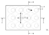
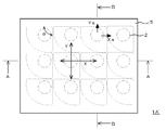
- FIG. 1A is a plan view of an anisotropic conductive film 1A according to an embodiment of the present invention.
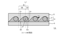
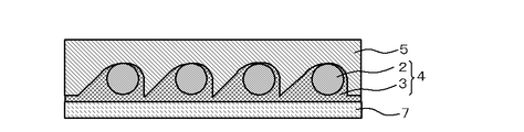
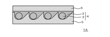
- FIG. 1B is a cross-sectional view of an anisotropic conductive film 1A according to an embodiment of the present invention.
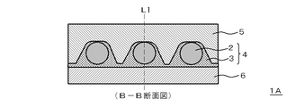
- FIG. 1C is a cross-sectional view of an anisotropic conductive film 1A according to an embodiment of the present invention.
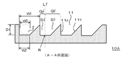
- FIG. 2A is a perspective view of a transfer mold 10A used for manufacturing the anisotropic conductive film 1A.
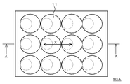
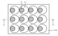
- FIG. 2B is a top view of the transfer mold 10A used for manufacturing the anisotropic conductive film 1A.
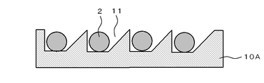
- FIG. 2C is a cross-sectional view of a transfer mold 10A used for manufacturing the anisotropic conductive film 1A.
- FIG. 1A is a plan view of an anisotropic conductive film 1A according to an embodiment of the present invention.
- FIG. 1B is a cross-sectional view of an anisotropic conductive film 1A according to an
- FIG. 3A is a top view of the transfer mold 10A filled with conductive particles.
- FIG. 3B is a cross-sectional view of the transfer mold 10A filled with conductive particles.
- FIG. 4A is an explanatory diagram of a manufacturing process of the anisotropic conductive film 1A.
- FIG. 4B is an explanatory diagram of the manufacturing process of the anisotropic conductive film 1A.
- FIG. 4C is an explanatory diagram of the production process of the anisotropic conductive film 1A.
- FIG. 4D is an explanatory diagram of the manufacturing process of the anisotropic conductive film 1A.
- FIG. 4E is an explanatory diagram of the manufacturing process of the anisotropic conductive film 1A.
- FIG. 4A is an explanatory diagram of a manufacturing process of the anisotropic conductive film 1A.
- FIG. 4F is an explanatory diagram of the manufacturing process of the anisotropic conductive film 1A.
- FIG. 4G is an explanatory diagram of the manufacturing process of the anisotropic conductive film 1A.
- FIG. 5A is an explanatory diagram of a manufacturing process of the anisotropic conductive film 1A.
- FIG. 5B is an explanatory diagram of the manufacturing process of the anisotropic conductive film 1A.
- FIG. 5C is an explanatory diagram of the manufacturing process of the anisotropic conductive film 1A.
- FIG. 5D is an explanatory diagram of the manufacturing process of the anisotropic conductive film 1A.
- FIG. 5E is an explanatory diagram of the production process of the anisotropic conductive film 1A.
- FIG. 6A is an explanatory diagram of the manufacturing process of the anisotropic conductive film 1A.
- FIG. 6B is an explanatory diagram of the manufacturing process of the anisotropic conductive film 1A.
- FIG. 6C is an explanatory diagram of the production process of the anisotropic conductive film 1A.
- FIG. 6D is an explanatory diagram of the manufacturing process of the anisotropic conductive film 1A.
- FIG. 6E is an explanatory diagram of the production process of the anisotropic conductive film 1A.
- FIG. 6F is an explanatory diagram of the manufacturing process of the anisotropic conductive film 1A.
- FIG. 6G is an explanatory diagram of the manufacturing process of the anisotropic conductive film 1A.
- FIG. 7A is a plan view of an anisotropic conductive film 1A ′ according to one embodiment of the present invention.
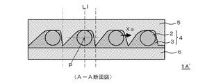
- FIG. 7B is a cross-sectional view of the anisotropic conductive film 1A ′ according to one embodiment of the present invention.
- FIG. 7C is a cross-sectional view of the anisotropic conductive film 1A ′ according to one embodiment of the present invention.
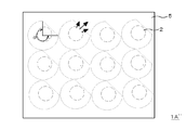
- FIG. 8 is a plan view of the anisotropic conductive film 1A ′′ according to the embodiment of the present invention.
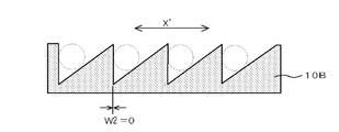
- FIG. 9A is a cross-sectional view of a transfer mold 10B filled with conductive particles.
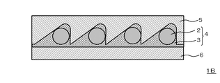
- FIG. 9B is a cross-sectional view of an anisotropic conductive film 1B obtained using the transfer mold 10B.
- FIG. 9A is a cross-sectional view of a transfer mold 10B filled with conductive particles.
- FIG. 10A is a cross-sectional view of a transfer mold 10C filled with conductive particles.
- FIG. 10B is a cross-sectional view of the anisotropic conductive film 1C obtained using the transfer mold 10C.
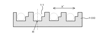
- FIG. 11A is a cross-sectional view of a transfer mold 10D filled with conductive particles.
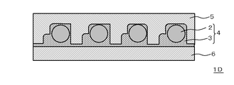
- FIG. 11B is a cross-sectional view of an anisotropic conductive film 1D obtained using the transfer mold 10D.
- FIG. 12A is a cross-sectional view of a transfer mold 10E filled with conductive particles.
- FIG. 12B is a cross-sectional view of an anisotropic conductive film 1E obtained using the transfer mold 10E.
- FIG. 13A is a cross-sectional view of a transfer mold 10X of a comparative example filled with conductive particles.
- FIG. 13B is a cross-sectional view of the anisotropic conductive film 1X obtained using the transfer mold 10X.
- FIG. 14 is an explanatory diagram of a method for evaluating the adhesive strength between an anisotropic conductively connected glass substrate and an IC chip.
- FIG. 1A is a plan view of an anisotropic conductive film 1A according to an embodiment of the present invention
- FIG. 1B is an AA sectional view
- FIG. 1C is a BB sectional view.
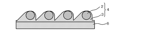
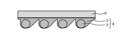
- the anisotropic conductive film 1A has a conductive particle array layer 4 in which a plurality of conductive particles 2 are directly held by an insulating resin layer 3, and the insulating resin layer 3 is made up of individual conductive films. It is characterized by having a specific thickness distribution to be described later around the particle 2.
- the conductive particle array layer 4 has one surface that is flat and the other surface is uneven, and the conductive particle array layer 4 has a second insulating resin layer 5 laminated on the uneven surface.
- a third insulating resin layer 6 is laminated on the flat surface.
- the second insulating resin layer 5 and the third insulating resin layer 6 are provided as necessary in order to improve the adhesiveness between the electronic components to be anisotropically conductively connected.
- (1-2) Conductive Particle Arrangement Layer In the conductive particle arrangement layer 4, a plurality of conductive particles 2 are arranged as a single layer in a tetragonal lattice. Further, the individual conductive particles 2 are respectively held by the insulating resin layer 3 at the convex portions of the conductive particle arrangement layer 4, and the insulating resin layer 3 around the individual conductive particles 2 has a substantially rounded corner. It has a truncated cone shape.
- the arrangement of the conductive particles 2 is not limited to a tetragonal lattice. For example, a hexagonal lattice may be used.
- the number of conductive particles held in the insulating resin layer 3 of one convex portion of the conductive particle array layer 4 is not limited to one, and may be plural.
- the shape of the insulating resin layer 3 forming the convex portion of the conductive particle array layer 4 is not limited to the oblique truncated cone, and may be, for example, a truncated cone shape such as an oblique rectangular truncated cone.
- This direction X is aligned in all the conductive particles 2.
- the individual conductive particles 2 area of the insulating resin layer 3 surrounding Q of the one area S a of the side Q a of the conductive particles 2 is smaller than the area S b of the other side Q b.
- the insulating resin layer 3 around the individual conductive particles 2 is the convex region of the insulating resin layer 3 holding the individual conductive particles 2 in the cross section, that is, in the cross section.
- the layer thickness of the insulating resin layer 3 (distance between the convex region side surface and the flat surface side region of the insulating resin layer 3) between the conductive particle 2 and the adjacent conductive particle 2 is the thinnest, It refers to the range up to the thinnest portion of the insulating resin layer 3 between the conductive particles 2 and the other adjacent conductive particles 2.
- one side surface 3 a side Q a of the conductive particles 2 has a cliff-like along the thickness direction of the anisotropic conductive film 1A
- the side surface 3 b of the other side Q b is inclined with respect to the thickness direction of the anisotropic conductive film 1A from the side surface 3 a of one side Q a.
- this anisotropic conductive film 1A has a direction X in which the thickness distribution of the insulating resin layer 3 around each conductive particle 2 is asymmetric with respect to the central axis L1 of the conductive particle 2.
- this direction X FIG. 1
- the area S a on one side Q a of the conductive particles 2 is smaller than the area S b on the other side Q b , and the insulation for holding the conductive particles 2 Since the resin amount of the conductive resin layer 3 is smaller on the one side Q a than on the other side Q b , the conductive particles at the time of heating and pressurizing when mounting the electronic component using the anisotropic conductive film 1A 2 is likely to flow in the small direction X a of the resin amount in the insulating resin layer 3 for holding the conductive particles 2 (FIG. 1A).
- the resin layer forming the surface of the anisotropic conductive film has surface irregularities, and the surface is formed of a flat resin layer. In comparison, it is expected that the tackiness of the anisotropic conductive film is increased and the adhesiveness is improved.
- the thickness distribution of the insulating resin layer 3 around the individual conductive particles 2 is asymmetric with respect to the conductive particles 2 is sufficient.
- the thickness distribution of the insulating resin layer 3 around the conductive particles 2 may be symmetric with respect to the conductive particles 2.
- the thickness distribution of the insulating resin layer 3 around the conductive particles 2 is as shown in FIG.
- the conductive particles 2 are symmetric with respect to the central axis L1.
- the conductive particles 2 can be appropriately selected from those used in conventionally known anisotropic conductive films. Examples thereof include metal particles such as nickel, cobalt, silver, copper, gold, and palladium, and metal-coated resin particles. Two or more kinds can be used in combination.
- the average particle diameter of the conductive particles 2 is preferably 1 to 10 ⁇ m, more preferably 2 to 6 ⁇ m.
- the number is 50 to 50000 per mm, more preferably 200 to 40000, and still more preferably 400 to 30000.
- a known insulating resin layer can be appropriately employed.
- a cationic polymerization type resin layer, a thermal anion polymerization type resin layer containing an epoxy compound and a thermal anion polymerization initiator, or the like can be used.
- these resin layers can be polymerized as necessary.
- the insulating resin layer 3 it is preferable to employ a photo radical polymerization type resin layer containing an acrylate compound and a photo radical polymerization initiator.
- the conductive particle arrangement layer 4 in which the conductive particles 2 are fixed to the insulating resin layer 3 can be formed by irradiating the photo radical polymerization type resin layer with ultraviolet rays to cause photo radical polymerization.
- photoradical polymerization resin layer is irradiated with ultraviolet rays from the conductive particle 2 side before the second insulating resin layer 5 is formed, photoradical polymerization is performed as shown in FIG. 4D.
- the curing rate of the region 3 m of the insulating resin layer 3 positioned between the flat surface of the conductive particle array layer 4 and the conductive particles 2 is determined by the insulating resin layer 3 positioned between the adjacent conductive particles 2. It can be made lower than the curing rate of the region 3n . Accordingly, the insulating resin layer 3, than the minimum melt viscosity of the high region 3 n the curing rate was around the minimum melt viscosity lower region 3 m of curing rate, the conductive particles 2 be in immediately below the conductive particles 2 In the anisotropic conductive connection, the conductive particles 2 are easily pushed in without being displaced in the horizontal direction. Therefore, the particle trapping efficiency can be improved, the conduction resistance value can be reduced, and good conduction reliability can be realized.
- the curing rate is a numerical value defined as a reduction ratio of functional groups (for example, vinyl groups) that contribute to polymerization. Specifically, if the vinyl group content after curing is 20% before curing, the curing rate is 80%. The abundance of vinyl groups can be measured by characteristic absorption analysis of vinyl groups in the infrared absorption spectrum.
- the curing rate of the region 3 m having a low curing rate of the insulating resin layer 3 is preferably 40 to 80%, and the curing rate of the region 3 n having a high curing rate is preferably 70 to 100%.
- the minimum melt viscosity of the insulating resin layer 3 can be measured with a rheometer. If this value is too low, the particle trapping efficiency tends to decrease, and if it is too high, the conduction resistance value tends to increase.
- the pressure is preferably 100 to 100,000 mPa ⁇ s, more preferably 500 to 50,000 mPa ⁇ s.
- the minimum melt viscosity of the insulating resin layer 3 is preferably higher than the minimum melt viscosity of each of the second insulating resin layer 5 and the third insulating resin layer 6. Specifically, the [minimum melt viscosity (mPa ⁇ s) of the insulating resin layer 3] / [minimum melt viscosity (mPa ⁇ s) of the second insulating resin layer 5 or the third insulating resin layer 6]. If the numerical value is too low, the particle trapping efficiency tends to decrease and the probability of occurrence of a short circuit tends to increase. If the numerical value is too high, the conduction reliability tends to decrease.
- the value of [minimum melt viscosity (mPa ⁇ s) of insulating resin layer 3] / [minimum melt viscosity (mPa ⁇ s) of second insulating resin layer 5 or third insulating resin layer 6] is obtained.
- the resin tends to protrude when the reel is formed. If it is too high, the conduction resistance value is high. Therefore, it is preferably 0.1 to 10000 mPa ⁇ s, more preferably 1 to 1000 mPa ⁇ s.
- acrylate compound used for the insulating resin layer 3 a conventionally known radical polymerizable acrylate can be used.
- monofunctional (meth) acrylate here, (meth) acrylate includes acrylate and methacrylate
- bifunctional or more polyfunctional (meth) acrylate can be used.
- polyfunctional (meth) acrylate in order to make the insulating resin layer 3 thermosetting, it is preferable to use polyfunctional (meth) acrylate for at least one part of an acryl-type monomer.
- Monofunctional (meth) acrylates include methyl (meth) acrylate, ethyl (meth) acrylate, n-propyl (meth) acrylate, i-propyl (meth) acrylate, n-butyl (meth) acrylate, i-butyl (meth) ) Acrylate, t-butyl (meth) acrylate, 2-methylbutyl (meth) acrylate, n-pentyl (meth) acrylate, n-hexyl (meth) acrylate, n-heptyl (meth) acrylate, 2-methylhexyl (meth) Acrylate, 2-ethylhexyl (meth) acrylate, 2-butylhexyl (meth) acrylate, isooctyl (meth) acrylate, isopentyl (meth) acrylate, isononyl (meth) acrylate, isode
- Bifunctional (meth) acrylates include bisphenol F-EO modified di (meth) acrylate, bisphenol A-EO modified di (meth) acrylate, polypropylene glycol di (meth) acrylate, polyethylene glycol (meth) acrylate, and tricyclodecanedi. Examples include methylol di (meth) acrylate and dicyclopentadiene (meth) acrylate.
- Examples of the trifunctional (meth) acrylate include trimethylolpropane tri (meth) acrylate, trimethylolpropane PO-modified (meth) acrylate, and isocyanuric acid EO-modified tri (meth) acrylate.
- tetrafunctional or higher functional (meth) acrylates examples include dipentaerythritol penta (meth) acrylate, pentaerythritol hexa (meth) acrylate, pentaerythritol tetra (meth) acrylate, and ditrimethylolpropane tetraacrylate.
- polyfunctional urethane (meth) acrylates can also be used. Specific examples include M1100, M1200, M1210, M1600 (above, Toagosei Co., Ltd.), AH-600, AT-600 (above, Kyoeisha Chemical Co., Ltd.) and the like.
- the content of the acrylate compound in the insulating resin layer 3 is too small, the minimum melt viscosity difference from the second insulating resin layer 5 tends to be difficult to be obtained. Since it tends to decrease, the content is preferably 2 to 70% by mass, more preferably 10 to 50% by mass.
- the photo radical polymerization initiator can be appropriately selected from known photo radical polymerization initiators. Examples include acetophenone photopolymerization initiators, benzyl ketal photopolymerization initiators, and phosphorus photopolymerization initiators.
- acetophenone photopolymerization initiator 2-hydroxy-2-cyclohexylacetophenone (IRGACURE 184, manufactured by BASF Japan Ltd.), ⁇ -hydroxy- ⁇ , ⁇ ′-dimethylacetophenone (Darocur) (DAROCUR) 1173, manufactured by BASF Japan Ltd., 2,2-dimethoxy-2-phenylacetophenone (IRGACURE 651, manufactured by BASF Japan Ltd.), 4- (2-hydroxyethoxy) phenyl (2-hydroxy-) 2-propyl) ketone (DAROCUR 2959, manufactured by BASF Japan Ltd.), 2-hydroxy-1- ⁇ 4- [2-hydroxy-2-methyl-propionyl] -benzyl ⁇ phenyl ⁇ -2-methyl-propane -1 One (IRGACURE (IRGACURE) 127, BASF Japan Ltd.) and the like.
- DAROCUR 2-hydroxy-2-cyclohexylacetophenone
- DAROCUR ⁇ -hydroxy- ⁇ , ⁇ ′-di
- benzyl ketal photoinitiators examples include benzophenone, fluorenone, dibenzosuberone, 4-aminobenzophenone, 4,4'-diaminobenzophenone, 4-hydroxybenzophenone, 4-chlorobenzophenone, 4,4'-dichlorobenzophenone, etc. It is done. Further, 2-benzyl-2-dimethylamino-1- (4-morpholinophenyl) -butanone-1 (IRGACURE 369, manufactured by BASF Japan Ltd.) can also be used.
- bis (2,4,6-trimethylbenzoyl) -phenylphosphine oxide (IRGACURE 819, manufactured by BASF Japan Ltd.), (2,4,6-trimethylbenzoyl-diphenylphossine) Examples include fin oxide (DAROCURE TPO, manufactured by BASF Japan Ltd.).
- the amount of the radical photopolymerization initiator used is too small relative to 100 parts by mass of the acrylate compound, the photoradical polymerization tends not to proceed sufficiently.
- the amount is preferably 0.1 to 25 parts by mass, more preferably 0.5 to 15 parts by mass.
- the insulating resin layer 3 is composed of a thermal radical polymerization type resin layer containing an acrylate compound and a thermal radical polymerization initiator
- the thermal radical polymerization initiator include organic peroxides and azo compounds.
- the azo compound decomposes during the polymerization reaction to generate nitrogen gas, and bubbles are generated in the polymer.
- An organic peroxide can be preferably used because it is feared to be mixed. Examples thereof include Perhexa 3M, Parroyl TCP, Parroyl L, etc. manufactured by Nippon Oil & Fats Co., Ltd.
- organic peroxides include methyl ethyl ketone peroxide, cyclohexanone peroxide, methylcyclohexanone peroxide, acetylacetone peroxide, 1,1-bis (tert-butylperoxy) 3,3,5-trimethylcyclohexane, 1,1-bis (Tert-butylperoxy) cyclohexane, 1,1-bis (tert-hexylperoxy) 3,3,5-trimethylcyclohexane, 1,1-bis (tert-hexylperoxy) cyclohexane, 1,1-bis ( tert-butylperoxy) cyclododecane, isobutyl peroxide, lauroyl peroxide, oxalic acid peroxide, 3,5,5-trimethylhexanoyl peroxide, benzoyl peroxide, octanoyl peroxide, steer Ile peroxide, diisopropy
- azo compounds include 1,1-azobis (cyclohexane-1-carbonitrile), 2,2'-azobis (2-methyl-butyronitrile), 2,2'-azobisbutyronitrile, 2,2'- Azobis (2,4-dimethyl-valeronitrile), 2,2'-azobis (2,4-dimethyl-4-methoxyvaleronitrile), 2,2'-azobis (2-amidino-propane) hydrochloride, 2, 2'-azobis [2- (5-methyl-2-imidazolin-2-yl) propane] hydrochloride, 2,2'-azobis [2- (2-imidazolin-2-yl) propane] hydrochloride, 2, 2'-azobis [2- (5-methyl-2-imidazolin-2-yl) propane], 2,2'-azobis [2-methyl-N- (1,1-bis (2-hydroxymethyl) -2 -Hydroxye L) propionamide], 2,2'-azobis [2-methyl-N- (2-hydroxyethy
- thermal radical polymerization initiator used is too small, there is a tendency that thermal radical polymerization does not proceed sufficiently, and if it is too large, there is a concern that it may cause a decrease in rigidity. Is 0.1 to 25 parts by mass, more preferably 0.5 to 15 parts by mass.
- the insulating resin layer 3 is composed of a thermal cationic polymerization type resin layer containing an epoxy compound and a thermal cationic polymerization initiator, or from a thermal anion polymerization type resin layer containing an epoxy compound and a thermal anionic polymerization initiator
- the epoxy compound is preferably a compound or resin having two or more epoxy groups in the molecule. These may be liquid or solid.
- a known epoxy resin such as epoxidized polyolefin may be used.
- alicyclic epoxy compounds such as 3,4-epoxycyclohexenylmethyl-3 ′, 4′-epoxycyclohexenecarboxylate can also be used.
- the thermal cationic polymerization initiator generates an acid that can cause cationic polymerization of a cationically polymerizable compound by heat.
- thermal cationic polymerization initiator those known as thermal cationic polymerization initiators for epoxy compounds can be employed, for example, known iodonium salts, sulfonium salts, phosphonium salts, ferrocenes, etc. can be used, An aromatic sulfonium salt exhibiting a good potential with respect to can be preferably used.
- thermal cationic polymerization initiator examples include diphenyliodonium hexafluoroantimonate, diphenyliodonium hexafluorophosphate, diphenyliodonium hexafluoroborate, triphenylsulfonium hexafluoroantimonate, triphenylsulfonium hexafluorophosphate, triphenyls.
- Rufonium hexafluoroborate is exemplified.
- the thermal cationic polymerization initiator If the amount of the thermal cationic polymerization initiator is too small, the thermal cationic polymerization tends not to proceed sufficiently, and if it is too large, there is a concern that it may cause a decrease in rigidity. Is 0.1 to 25 parts by mass, more preferably 0.5 to 15 parts by mass.
- the thermal anionic polymerization initiator generates a base that can anionically polymerize the anionic polymerizable compound by heat.
- the thermal cationic polymerization initiator those known as the thermal anionic polymerization initiator of the epoxy compound can be employed.
- An imidazole compound, a polymercaptan compound, a boron trifluoride-amine complex, dicyandiamide, an organic acid hydrazide, or the like can be used, and an encapsulated imidazole compound showing good potential with respect to temperature is preferably used. it can.
- the amount is preferably 0.1 to 100 parts by mass with respect to 100 parts by mass of the epoxy compound.
- the amount is 40 parts by mass, more preferably 0.5 to 20 parts by mass.
- the second insulating resin layer 5 and the third insulating resin layer 6 can be formed of a resin appropriately selected from known insulating resins. You may form from the material similar to the insulating resin layer 3. FIG.
- the minimum melt viscosity of the insulating resin layer 3 can be equal to or greater than or equal to that of the second and third insulating resin layers 5 and 6, but the second insulating resin layer 5 and the third When the insulating resin layer 6 is formed of the same material as the insulating resin layer 3, the minimum melt viscosity of the insulating resin layer 3 is higher than that of the second and third insulating resin layers 5 and 6. It is preferable.
- the thickness of the second insulating resin layer 5 is too thin, there is a concern that poor conduction due to insufficient resin filling will occur, and if it is too thick, there is a concern that the resin will protrude when it is pressed and the crimping device will be contaminated. Therefore, it is 40 ⁇ m or less, preferably 5 to 20 ⁇ m, more preferably 8 to 15 ⁇ m. If the layer thickness of the third insulating resin layer 6 is too thin, there is a concern that a sticking failure may occur when temporarily sticking to the second electronic component, and if it is too thick, the conduction resistance value tends to increase. Is 0.5 to 6 ⁇ m, more preferably 1 to 5 ⁇ m.
- the thinner resin layer is usually relatively high, such as a solid electrode of a glass substrate. It is arranged on the terminal side where alignment accuracy is not required, and the thicker one is usually arranged on the terminal side that requires alignment with high positional accuracy such as bumps of the IC chip.
- the side closer to the conductive particles is the side with relatively low alignment accuracy. In the case where neither is provided, there is no particular limitation.
- FIG. 2B is a top view of the transfer mold 10A
- FIG. 2C is a cross-section of the transfer mold 10A.
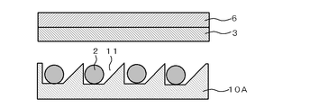
- This transfer mold 10A has a plurality of openings 11 arranged in a tetragonal lattice on the surface, and the depth distribution in each opening 11 is a vertical line L1 ′ passing through the center R of the deepest part of the opening 11. It has a direction X ′ that is asymmetric with respect to it. More specifically, in the cross section (FIG. 2C) of the transfer mold 10A when the transfer mold 10A is cut in the direction X ′ passing through the center R of the deepest part of the opening 11, the center R of the deepest part of the opening 11 is vertical line L1 area S a of the opening 10 'of one side Q a of' through 'is the other side Q b' smaller than the area S b 'of.
- the arrangement of the openings is appropriately selected according to the arrangement of the conductive particles in the anisotropic conductive film to be manufactured. For example, when the conductive particles are arranged in a six-way lattice, the transfer is performed.
- the arrangement of the mold openings is also a hexagonal lattice.
- the other side Q b ′ side wall 11 b is inclined with respect to the side wall 11 a on one side Q a ′. That is, the side wall 11 a on one side Q a ′ has a cliff shape standing in the thickness direction of the transfer mold 10, and the side wall 11 b on the other side Q b ′ is inclined with respect to the thickness direction of the transfer mold 10. ing.
- the depth D1 of the opening 11 is determined by the ease of work for removing the conductive particle array layer 4 formed on the transfer mold 10A from the transfer mold 10A. From the viewpoint of balance with the retention of the conductive particles 2, the ratio (W 0 / D 1) between the average particle diameter W 0 of the conductive particles 2 filled in the openings 11 and the depth D 1 of the openings 11 is preferably set to 0. 4 to 3.0, more preferably 0.5 to 1.5.
- the relationship between the opening diameter W1 of the opening 11 and the average particle diameter W0 of the conductive particles 2 is as follows.
- the ratio of the opening diameter W1 of the opening 11 to the average particle diameter W0 of the conductive particle 2 (W1 / W0) from the viewpoint of easy filling of the conductive particle 2 into the opening 11 and ease of pushing the insulating resin into the opening 11 ) Is preferably 1.2 to 5.0, more preferably 1.5 to 3.0.
- the relationship between the bottom diameter W2 of the opening 11 and the average particle diameter W0 of the conductive particles 2 is such that the flow direction of each conductive particle 2 during thermocompression bonding is aligned.
- the average particle diameter W0 of the conductive particles 2 (W2 / W0) is preferably 0 to 1.9, more preferably 0 to 1.6.
- the transfer mold 10A As a forming material of the transfer mold 10A, for example, inorganic materials such as silicon, various ceramics, glass, stainless steel, and other organic materials, and organic materials such as various resins can be used.
- the opening 11 is formed by a photolithographic method. It can form by well-known opening formation methods, such as.
- the conductive particles 2 are filled into the opening 11 of the transfer mold 10A.
- the method for filling the conductive particles 2 is not particularly limited.
- the dried conductive particles 2 or a dispersion of the conductive particles 2 in which the conductive particles 2 are dispersed in a solvent is sprayed or applied onto the surface on which the opening 11 of the transfer mold 10A is formed.
- the formation surface of the opening 11 may be wiped using a brush or cloth. By conducting this wipe from the bottom of the inclined side wall 11 b of the opening 11 along the direction X ′, the conductive particles 2 can be smoothly fed into the opening 11.
- the conductive particles 2 may be dispersed on the formation surface of the opening 11 of the transfer mold 10 ⁇ / b> A and then moved to the opening 11 using an external force such as a magnetic field. Good.
- the insulating resin layer 3 formed on the release film 7 is laminated on the opening 11 filled with the conductive particles 2 so as to face each other and insulated at the bottom corner of the opening 11. Pressure is applied to such an extent that the conductive resin layer 3 does not enter, and the conductive particles 2 are held in the insulating resin layer 3 so that the conductive particles 2 are embedded in the insulating resin layer 3 as shown in FIG. 4B.
- the conductive particle array in which the conductive particles 2 arranged in a tetragonal lattice according to the arrangement of the openings 11 of the transfer mold 10A are held in the insulating resin layer 3 is provided.
- Layer 4 can be obtained on release film 7.
- the conductive particles 2 do not have to be completely embedded in the insulating resin layer 3 but may be embedded.
- the conductive particles 2 at the bottom of the transfer mold 10A can be moved to the opening surface side of the transfer mold 10A. This movement may be performed by an external force such as a magnetic force.
- the conductive particles 2 can be fixed to the insulating resin layer 3.
- the UV irradiation is blocked by the conductive particles 2, so that the curing rate is relatively low compared to the surroundings. Therefore, in anisotropic conductive connection, the conductive particles 2 are easily pushed in without being displaced in the horizontal direction. Therefore, the particle trapping efficiency can be improved, the conduction resistance value can be reduced, and good conduction reliability can be realized.
- the second insulating resin layer 5 is laminated on the surface of the conductive particle array layer 4 with the surface irregularities (that is, the transfer surface of the conductive particles 2 in the insulating resin layer 3).
- the release film 7 is peeled off and removed, and as shown in FIG. 4G, the surface from which the release film 7 has been peeled (that is, the side opposite to the transfer surface of the conductive particles 2 in the insulating resin layer 3).
- the third insulating resin layer 6 is laminated on the surface).
- the anisotropic conductive film 1A shown in FIGS. 1A, 1B, and 1C can be manufactured.
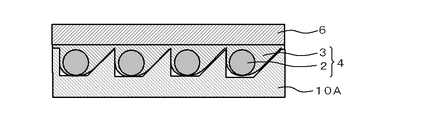
- the conductive particles 2 are filled into the openings 11 of the transfer mold 10A, and then the conductive particles 2 are filled into the openings 11 as shown in FIG. 5A.
- the insulating resin layer 3 on which the third insulating resin layer 6 is pasted in advance is laminated oppositely.
- the insulating resin layer 3 is pushed into the formation surface of the opening 11 of the transfer mold 10 ⁇ / b> A to hold the conductive particles 2 in the insulating resin layer 3, thereby forming the conductive particle array layer 4. .
- the laminate of the conductive particle array layer 4 and the third insulating resin layer 6 is taken out from the transfer mold 10A, and as shown in FIG. 5D, from the uneven surface side of the insulating resin layer 3.
- the conductive particles 2 are fixed to the insulating resin layer 3 by UV irradiation.
- the second insulating resin layer 5 is laminated on the uneven surface of the insulating resin layer 3.
- the anisotropic conductive film 1A shown in FIGS. 1A, 1B, and 1C can be manufactured.
- the conductive particles 2 are filled in the opening of the UV-transmissive transfer mold 10A ′, and then, as shown in FIG. 6A, the conductive particles 2 are filled.
- the photopolymerizable insulating resin layer 3 formed on the release film 7 is opposed to the opening 11 of the transfer mold 10A ′ in which the opening 11 is filled.
- the insulating resin layer 3 is pressurized to such an extent that it does not enter the conductive resin 2 so that the conductive particles 2 are embedded in the insulating resin layer 3 as shown in FIG. 6B.
- the alignment layer 4 is formed. Also in this case, the conductive particles 2 may be completely embedded in the insulating resin layer 3 or may not be completely embedded.
- the ultraviolet rays UV are applied to the insulating resin layer 3 from the transfer mold 10A ′ side.
- the photopolymerizable insulating resin layer 3 can be polymerized, and the conductive particles 2 can be fixed to the insulating resin layer 3, and the ultraviolet rays UV can be blocked by the conductive particles 2.
- the curing rate of the region 3 m can be made relatively lower than the curing rate of the region 3 n of the surrounding insulating resin layer. Therefore, the pushability of the conductive particles 2 can be improved while preventing the horizontal displacement of the conductive particles 2 during anisotropic conductive connection. Therefore, the particle trapping efficiency can be improved, the conduction resistance value can be reduced, and good conduction reliability can be realized.
- the release film 7 is removed from the insulating resin layer 3.
- the third insulating resin layer 6 is laminated on the surface of the insulating resin layer 3 from which the release film 7 has been removed, and the laminate is transferred to the transfer mold 10A ′ as shown in FIG. 6F.
- the second insulating resin layer 5 is laminated on the surface of the conductive particle array layer 4 with the surface irregularities.
- the anisotropic conductive film 1A shown in FIGS. 1A, 1B, and 1C can be manufactured.
- Modification (3-1) Direction in which thickness distribution of insulating resin layer around conductive particles becomes asymmetrical
- the anisotropic conductive film of the present invention directly holds a plurality of conductive particles 2 in a predetermined arrangement.
- the thickness distribution of the insulating resin layer 3 around each conductive particle 2 may have a plurality of directions that are asymmetric with respect to the central axis L 1 of the conductive particle 2.
- the shape of the insulating resin layer 3 around each conductive particle 2 in a plan view can be substantially fan-shaped.
- the thickness distribution of the resin layer 3 is asymmetric with respect to the central axis L 1 of the conductive particles 2.
- the conductive particles 2 flow in two directions X a and Y a with a small amount of resin holding the conductive particles 2. It becomes easy.
- conductive particles flow irregularly due to heating and pressurization during mounting, and conductive particles between electrodes due to the concentration of conductive particles, and poor conduction due to the absence of conductive particles between electrodes. Can be reduced. Further, in the case of the anisotropic conductive film 1A ′′ of FIG. 8, the conductive particles 2 easily flow in the direction of the arrow.
- the thickness distribution of the insulating resin layer 3 around the individual conductive particles 2 is made uniform throughout the anisotropic conductive film, and the conductive particles 2 flow at the time of anisotropic conductive connection.
- the direction of facilitating may be aligned for all the conductive particles 2, and the thickness distribution of the insulating resin layer 3 around each of the conductive particles 2 may be different for each predetermined region in the anisotropic conductive film.
- the direction in which the conductive particles 2 easily flow during the isotropic conductive connection may be varied for each predetermined region of the anisotropic conductive film.
- the thickness distribution of the insulating resin layer 3 around each conductive particle 2 has a direction that is asymmetric with respect to the central axis L 1 of the conductive particle 2.
- the thickness of the insulating resin layer 3 holding a plurality of conductive particles 2 in a predetermined arrangement The insulating resin layer 3 can take various shapes so that the thickness distribution is asymmetric in a specific direction around each conductive particle 2. Therefore, the transfer mold used for forming the insulating resin layer 3 also has a direction X in which the depth distribution in the opening 11 is asymmetric with respect to the vertical line L1 ′ passing through the center R of the deepest portion of the opening 11. Various shapes can be taken to have a '.
- the bottom surface of the opening 11 may be formed into a rough surface having small irregularities. Thereby, the area where the conductive particles 2 are in contact with the transfer mold 10A is reduced, and the work of removing the conductive particle array layer from the transfer mold 10A is facilitated.
- the opening 11 in the cross section (FIG. 2C) when the transfer mold 10A is cut in the direction X ′ passing through the center R of the deepest portion of the opening 11, the opening 11
- the width W2 of the bottom surface of the opening 11 may be zero as in the transfer mold 10B shown in FIG. 9A.
- the transfer mold 10A shown in FIGS. 2A, 2B and 2C the transfer mold 10A is shown in a cross section (FIG. 2C) when the transfer mold 10A is cut in the direction X ′ passing through the center R of the deepest portion of the opening 11.
- a predetermined distance W3 may be provided between the adjacent openings on the upper surface of the transfer mold as in the transfer mold 10C shown in FIG. 10A.
- the number of steps can be changed as appropriate, and for example, it can be three steps as in the transfer mold 10E shown in FIG. 12A.
- this transfer mold 10E an anisotropic conductive film 1E having a cross section shown in FIG. 12B can be obtained.
- the conductive particles 2 may be partially exposed from the insulating resin layer 3.
- the depth distribution in each opening is symmetric in a cross section in any direction including a vertical line passing through the center of the deepest part of the opening (for example, a cliff-like one whose entire circumference of the side wall of the opening portion stands in the thickness direction of the transfer mold may be used.
- a cliff-like one whose entire circumference of the side wall of the opening portion stands in the thickness direction of the transfer mold may be used.
- the thickness distribution of the insulating resin layer that holds the conductive particles in the conductive film may be asymmetric with respect to the conductive particles.
- the conductive particles 2 easily flow in a specific direction at the time of anisotropic conductive connection.
- the opening 11 of the transfer mold 10X is bilaterally symmetric as shown in FIG. 13A in an arbitrary direction
- the obtained anisotropic conductive film 1X holds the conductive particles 2 as shown in FIG. 13B.
- the thickness distribution around the insulating resin layer 3 is symmetric in an arbitrary direction around the conductive particles 2, and the flow direction of the conductive particles is not determined during anisotropic conductive connection. For this reason, it is impossible to avoid the occurrence of short-circuits caused by continuous conductive particles between the electrodes and the occurrence of poor conduction due to the absence of conductive particles between the electrodes.
- the present invention includes a connection structure in which the first electronic component and the second electronic component are anisotropically conductively connected with the anisotropic conductive film of the present invention.
- Examples 1 to 5 and Comparative Example 1 Manufacture of anisotropic conductive film
- a transfer mold used in each example and comparative example a transfer mold made of stainless steel having the following shapes and dimensions (a) to (f) is prepared.
- An anisotropic conductive film was produced according to the method shown in FIG. 4G.
- Example 1 having the same shape as the transfer mold 10A shown in FIGS. 2A to 2C and having the dimensions shown in Table 1
- Example 2 In the transfer mold 10A shown in FIGS. 2A to 2C, the AA cross-section has the shape shown in FIG. 10A and has the dimensions shown in Table 1.
- Example 3 Same shape as (b), having dimensions shown in Table 1
- Example 4 In the transfer mold 10A shown in FIGS. 2A to 2C, the AA cross section is the shape shown in FIG. 11A and has the dimensions shown in Table 1.
- Example 5 In the transfer mold 10A shown in FIGS. 2A to 2C, the AA cross section is the shape shown in FIG. 12A and has the dimensions shown in Table 1.
- Comparative Example 1 In the transfer mold 10A shown in FIGS. 2A to 2C, the AA cross section is the shape shown in FIG. 13A and has the dimensions shown in Table 1.
- phenoxy resin (YP-50, Nippon Steel & Sumikin Chemical Co., Ltd.), 40 parts by mass of acrylate (EB-600, Daicel Ornex Co., Ltd.), and 2 parts by mass of radical photopolymerization initiator (IRUGACURE 369, BASF Japan Ltd.)
- IRUGACURE 369 radical photopolymerization initiator
- a polyethylene terephthalate film (PET film) having a thickness of 50 ⁇ m is prepared as a release film, and the above-mentioned mixed liquid is applied to the release film so that the dry thickness is 5 ⁇ m, and the film is placed in an oven at 80 ° C. By drying for a minute, a radical photopolymerization type insulating resin layer was formed.
- the above-mentioned insulating resin layer is made to face the opening surface of the transfer mold, and the conductive particles are pushed into the insulating resin layer by pressing from the release film side under the condition of 0.5 MPa at 60 ° C.
- a conductive particle array layer 4 in which the particles 2 are held on the insulating resin layer 3 was formed (FIG. 4B).
- the conductive particle array layer 4 is removed from the transfer mold 10A (FIG. 4C), and the surface of the insulating resin layer 3 on which the surface irregularities are formed is irradiated with ultraviolet rays having a wavelength of 365 nm and an integrated light amount of 4000 mJ / cm 2.
- the conductive particles 2 were fixed to the insulating resin layer 3 (FIG. 4D).
- phenoxy resin (YP-50, Nippon Steel & Sumikin Chemical Co., Ltd.), 40 parts by mass of epoxy resin (iER828, Mitsubishi Chemical Co., Ltd.), 2 parts by thermal cationic polymerization initiator (SI-60L, Sanshin Chemical Industry Co., Ltd.)
- SI-60L thermal cationic polymerization initiator
- the second insulating resin layer 5 is laminated under the conditions of 60 ° C. and 0.5 MPa. (FIG. 4E) Subsequently, the release film 7 on the opposite surface is removed (FIG. 4F), and the third insulating resin layer 6 is laminated on the removal surface of the release film 7 in the same manner as the second insulating resin layer. An anisotropic conductive film was obtained (FIG. 4G).
- IC dimensions 1.8 ⁇ 20.0 mm, thickness 0.5 mm, bump size 30 ⁇ 85 ⁇ m, bump height 15 ⁇ m, bump pitch 50 ⁇ m
- Glass substrate manufactured by Corning, 1737F, size 50 ⁇ 30 mm, thickness 0.5 mm
- the probe 22 was applied to the IC 21 on the glass substrate 20 to apply a shearing force in the direction of the arrow, and the force when the IC 21 peeled was measured. .
- the anisotropic conductive films of Examples 1 to 5 have significantly fewer connected particles and a lower incidence of short-circuit than the anisotropic conductive film of Comparative Example 1.
- the anisotropic conductive films of Examples 1 to 5 are superior in bonding strength to the anisotropic conductive film of Comparative Example 1, which is the same as the anisotropic conductive films of Examples 1 to 5.
- the thickness distribution of the insulating resin layer that directly contacts the conductive particles is asymmetric with respect to the conductive particles, and the unevenness of the insulating resin layer affects the surface unevenness of the anisotropic conductive film. This is presumed to be due to the increased nature.
- the present invention is useful as a technique for anisotropically connecting an ionization component such as an IC chip to a wiring board.
Landscapes
- Engineering & Computer Science (AREA)
- Manufacturing & Machinery (AREA)
- Microelectronics & Electronic Packaging (AREA)
- Physics & Mathematics (AREA)
- Chemical & Material Sciences (AREA)
- Dispersion Chemistry (AREA)
- Spectroscopy & Molecular Physics (AREA)
- Non-Insulated Conductors (AREA)
- Manufacturing Of Electrical Connectors (AREA)
- Adhesive Tapes (AREA)
- Adhesives Or Adhesive Processes (AREA)
- Conductive Materials (AREA)
Abstract
Description
複数の開口部を表面に有する転写型に導電粒子を充填する工程、
導電粒子上に絶縁性樹脂を積層する工程、及び
複数の導電粒子が所定の配列で絶縁性樹脂層に保持され、転写型から絶縁性樹脂層に転写されている導電粒子配列層を形成する工程を有し、
転写型として、個々の開口部における深さ分布が、開口部の最深部の中心を通る鉛直線に対して非対称となる方向を有するものを使用する製造方法を提供する。
(1)異方性導電フィルムの構成
(1-1)全体構成
図1Aは、本発明の一実施形態の異方性導電フィルム1Aの平面図、図1BはそのA-A断面図、図1CはB-B断面図である。
導電粒子配列層4では、複数の導電粒子2が単層で4方格子に配列している。また、個々の導電粒子2は、それぞれ導電粒子配列層4の凸部において絶縁性樹脂層3に保持され、個々の導電粒子2の周囲の絶縁性樹脂層3は、概ね角がまるめられた斜円錐台形状を有している。
なお、本発明において、導電粒子2の配列は、4方格子に限定されない。例えば、6方格子等でもよい。導電粒子配列層4の1つの凸部の絶縁性樹脂層3に保持される導電粒子の数は、1個に限られず、複数でもよい。
また、本発明において、導電粒子配列層4の凸部をなす絶縁性樹脂層3の形状は、斜円錐台に限られず、例えば、斜矩形錐台等の錐台形状等とすることができる。
異方性導電フィルム1Aにおいて、導電粒子2としては、従来公知の異方性導電フィルムに用いられているものの中から適宜選択して使用することができる。例えば、ニッケル、コバルト、銀、銅、金、パラジウムなどの金属粒子、金属被覆樹脂粒子などが挙げられる。2種以上を併用することもできる。
導電粒子2を保持する絶縁性樹脂層3としては、公知の絶縁性樹脂層を適宜採用することができる。例えば、アクリレート化合物と光ラジカル重合開始剤とを含む光ラジカル重合型樹脂層、アクリレート化合物と熱ラジカル重合開始剤とを含む熱ラジカル重合型樹脂層、エポキシ化合物と熱カチオン重合開始剤とを含む熱カチオン重合型樹脂層、エポキシ化合物と熱アニオン重合開始剤とを含む熱アニオン重合型樹脂層等を使用することができる。また、これらの樹脂層は、必要に応じて、それぞれ重合したものとすることができる。
(2-1)転写型
異方性導電フィルム1Aは、例えば、次のように転写型を用いて製造することができる。即ち、図2Aは、異方性導電フィルム1Aの製造に使用することのできる転写型10Aの斜視図であり、図2Bは、その転写型10Aの上面図、図2Cは、転写型10Aの断面図である。
異方性導電フィルム1Aの製造方法においては、まず、図3A、図3Bに示すように、転写型10Aの開口部11に導電粒子2を充填する。導電粒子2の充填方法は特に限定されず、例えば、乾燥した導電粒子2またはこれを溶媒中に分散させた導電粒子2の分散液を転写型10Aの開口部11の形成面上に散布または塗布し、次いでブラシや布などを用いて開口部11の形成面をワイプすればよい。このワイプを、前述の方向X’に沿って、開口部11の傾斜した側壁11bの底部から上部方向へ行うことにより、開口部11内に導電粒子2を円滑に送り込むことができる。
図1A、図1B及び図1Cに示した異方性導電フィルム1Aの製造方法は、上述の例に限られない。例えば、上述の製造方法において、剥離フィルム7に代えて、第3の絶縁性樹脂層6を形成してもよい。
図1A、図1B及び図1Cに示した異方性導電フィルム1Aの製造方法において、紫外線透過性の転写型10A’を使用した場合には、導電粒子2が保持された絶縁性樹脂層3への紫外線照射を転写型10A’を通して行ってもよい。紫外線透過性の転写型10A’は、紫外線透過性ガラス等の無機材料、あるいはポリメタクリレート等の有機材料から形成することができる。
(3-1)導電粒子の周囲における絶縁性樹脂層の厚さ分布が非対称となる方向
本発明の異方性導電フィルムは、複数の導電粒子2を所定の配列で直接的に保持している絶縁性樹脂層3に関し、個々の導電粒子2の周囲における絶縁性樹脂層3の厚さ分布が、導電粒子2の中心軸L1に対して非対称となる方向を複数有していてもよい。例えば、図7A、図7B及び図7Cに示す異方性導電フィルム1A’のように、個々の導電粒子2の周囲の絶縁性樹脂層3の平面視の形状を略扇形とすることができる。この扇形の開きの角度αにより非対称性は任意の形状を取ることができ、α=90°の扇形(図7A)、α=180°の半円形等とすることができる。また、図8に示すように、中心角α(例えば、α=270°)の円弧と弦からなる部分円としてもよい。
また、図8の異方性導電フィルム1A’’の場合、導電粒子2は矢印方向に流動し易くなる。
本発明の異方性導電フィルムにおいては、複数の導電粒子2を所定の配列に保持している絶縁性樹脂層3の厚さ分布が個々の導電粒子2の周囲において特定の方向で非対称となるように、絶縁性樹脂層3は種々の形状をとることができる。したがって、絶縁性樹脂層3を形成するために使用する転写型も、開口部11における深さ分布が、開口部11の最深部の中心Rを通る鉛直線L1’に対して非対称となる方向X’を有するように、種々の形状をとることができる。
(1)異方性導電フィルムの製造
各実施例及び比較例で使用する転写型として、次の(a)~(f)の形状及び寸法を有するステンレススチール製の転写型を用意し、図4A~図4Gに示した方法に準じて異方性導電フィルムを製造した。
(b)実施例2:図2A~図2Cに示した転写型10Aにおいて、A-A断面を図10Aに示す形状とし、表1に示す寸法を有するもの
(c)実施例3:(b)と同様の形状で、表1に示す寸法を有するもの
(d)実施例4:図2A~図2Cに示した転写型10Aにおいて、A-A断面を図11Aに示す形状とし、表1に示す寸法を有するもの
(e)実施例5:図2A~図2Cに示した転写型10Aにおいて、A-A断面を図12Aに示す形状とし、表1に示す寸法を有するもの
(f)比較例1:図2A~図2Cに示した転写型10Aにおいて、A-A断面を図13Aに示す形状とし、表1に示す寸法を有するもの
各実施例及び比較例で得た異方性導電フィルムに対して、(i)接合強度、(ii)連結粒子数、(iii)絶縁性(ショート発生率)を次のように評価した。結果を表1に示す。
各実施例及び比較例で得た異方性導電フィルムを使用し、次のICとガラス基板からなる導通評価用部材を、180℃、80MPaで5秒間加熱加圧することにより、実装サンプルを作成した。
ガラス基板:コーニング社製、1737F、サイズ 50×30mm、厚さ0.5mm
次に、デイジ社製ボンドテスターを用いて、図14に示すように、ガラス基板20上のIC21にプローブ22を当てて矢印の方向に剪断力を加え、IC21が剥離するときの力を測定した。
実装サンプルの接続領域(端子同士の接合部分を除く)の40000μm2を微鏡観察することにより、連結している導電粒子数の最大値を数えた。
各実施例及び比較例で得た異方性導電フィルムを使用し、(i)と同様の接合条件で7.5μmスペースの櫛歯TEG(test element group)パターン同士を接続し、ショート発生率を求めた。実用上、100ppm以下であることが望ましい。ショート発生率は、「ショートの発生数/7.5μmスペース総数」で算出される。

2 導電粒子
3 絶縁性樹脂層
3a、3b 側面
3m、3n 領域
4 導電粒子配列層
5 第2の絶縁性樹脂層
6 第3の絶縁性樹脂層
7 剥離フィルム
10A、10A’、10B、10C、10D、10E、10X 転写型
11 開口部
11a、11b 開口部の側壁
20 ガラス基板
21 IC
22 プローブ
D1 開口部の深さ
L1 導電粒子の中心軸
L1’ 転写型の開口部の最深部の中心を通る鉛直線
P 導電粒子の中心
Q 導電粒子の周囲
Qa 導電粒子の一方の側面
Qb 導電粒子の他方の側面
R 転写型の開口部の最深部の中心
Sa、Sa’、Sb、Sb’ 面積
W0 導電粒子の平均粒径
W1 開口部の開口径
W2 開口部の底面径
W3 開口部間の距離
X、Xa、X’、Y、Ya 方向
Claims (16)
- 複数の導電粒子が所定の配列で絶縁性樹脂層に保持されている導電粒子配列層を有する異方性導電フィルムであって、導電粒子の配列を保持している絶縁性樹脂層の個々の導電粒子の周囲における厚さ分布が、該導電粒子に対して非対称となる方向を有する異方性導電フィルム。
- 前記非対称となる方向が、複数の導電粒子について揃っている請求項1記載の異方性導電フィルム。
- 導電粒子の中心を通る、前記非対称となる方向で異方性導電フィルムを切断した場合の異方性導電フィルムの断面において、該導電粒子の周囲の絶縁性樹脂層の面積につき、導電粒子の一方の側の面積が、他方の側の面積に比して小さい請求項1又は2記載の異方性導電フィルム。
- 導電粒子の中心を通る、前記非対称となる方向で異方性導電フィルムを切断した場合の異方性導電フィルムの断面において、該導電粒子の周囲の絶縁性樹脂層は一方の側面が異方性導電フィルムの厚み方向に起立した断崖状であり、他方の側面が、前記一方の側面よりも異方導電性フィルムの厚さ方向に対して傾いている請求項3記載の異方性導電フィルム。
- 導電粒子の中心を通る、前記非対称となる方向で異方性導電フィルムを切断した場合の異方性導電フィルムの断面において、該導電粒子の周囲の絶縁性樹脂層は一方の側面が異方性導電フィルムの厚み方向に起立した断崖状であり、他方の側面が階段状である請求項3記載の異方性導電フィルム。
- 導電粒子配列層の一方の面が平坦で、他方の面が凹凸を有し、該凹凸を有する面に、第2の絶縁性樹脂層が積層されている請求項1~5のいずれかに記載の異方性導電フィルム。
- 導電粒子配列層の平坦な面に、第3の絶縁性樹脂層が積層されている請求項6記載の異方性導電フィルム。
- 請求項1記載の異方性導電フィルムの製造方法であって、
複数の開口部を表面に有する転写型に導電粒子を充填する工程、
導電粒子上に絶縁性樹脂を積層する工程、及び
複数の導電粒子が所定の配列で絶縁性樹脂層に保持され、転写型から絶縁性樹脂層に転写されている導電粒子配列層を形成する工程を有し、
転写型として、個々の開口部における深さ分布が、開口部の最深部の中心を通る鉛直線に対して非対称となる方向を有するものを使用する製造方法。 - 開口部の最深部の中心部を通る、前記非対称となる方向で転写型を切断した場合の転写型の断面において、開口部の最深部の中心を通る鉛直線の一方の側の開口部の面積が、他方の側の面積に比して小さい請求項8記載の製造方法。
- 開口部の最深部の中心部を通る、前記非対称となる方向で転写型を切断した場合の転写型の断面において、開口部の対向する側壁の一方が転写型の厚み方向に断崖状に起立し、他方が前記一方の側壁よりも異方導電性フィルムの厚さ方向に対して傾いている請求項8又は9記載の製造方法。
- 開口部の最深部の中心部を通る、前記非対称となる方向で転写型を切断した場合の転写型の断面において、開口部の対向する側壁の一方が転写型の厚み方向に断崖状に起立し、他方が階段状である請求項8又は9記載の製造方法。
- 導電粒子配列層を形成する工程において、絶縁性樹脂層を重合する請求項8~11のいずれかに記載の製造方法。
- 絶縁性樹脂として光ラジカル重合型樹脂を使用し、導電粒子上に積層した絶縁性樹脂を、紫外線の照射により重合する請求項8~12記載の製造方法。
- 絶縁性樹脂層の、導電粒子の転写面上に第2の絶縁性樹脂層を積層する請求項8~13記載の製造方法。
- 絶縁性樹脂層の、導電粒子の転写面と反対側の面に第3の絶縁性樹脂層を積層する請求項14記載の製造方法。
- 請求項1~7のいずれかに記載の異方性導電フィルムで第1電子部品と第2電子部品とが異方性導電接続されている接続構造体。
Priority Applications (9)
| Application Number | Priority Date | Filing Date | Title |
|---|---|---|---|
| US14/904,519 US20160155717A1 (en) | 2013-07-31 | 2014-07-29 | Anisotropic conductive film and manufacturing method therefor |
| CN201480039798.9A CN105359342B (zh) | 2013-07-31 | 2014-07-29 | 各向异性导电膜及其制造方法 |
| KR1020167000729A KR101987917B1 (ko) | 2013-07-31 | 2014-07-29 | 이방성 도전 필름 및 그의 제조 방법 |
| HK16105225.8A HK1217381B (en) | 2013-07-31 | 2014-07-29 | Anisotropically conductive film and manufacturing method therefor |
| KR1020197015980A KR102149375B1 (ko) | 2013-07-31 | 2014-07-29 | 이방성 도전 필름 및 그의 제조 방법 |
| CN201810058617.7A CN109087900B (zh) | 2013-07-31 | 2014-07-29 | 各向异性导电膜及其制造方法 |
| US16/176,923 US20190067234A1 (en) | 2013-07-31 | 2018-10-31 | Anisotropic conductive film and manufacturing method thereof |
| US16/206,628 US20190096844A1 (en) | 2013-07-31 | 2018-11-30 | Anisotropic conductive film and manufacturing method thereof |
| US17/328,336 US20210280548A1 (en) | 2013-07-31 | 2021-05-24 | Anisotropic conductive film and manufacturing method thereof |
Applications Claiming Priority (2)
| Application Number | Priority Date | Filing Date | Title |
|---|---|---|---|
| JP2013-159441 | 2013-07-31 | ||
| JP2013159441 | 2013-07-31 |
Related Child Applications (3)
| Application Number | Title | Priority Date | Filing Date |
|---|---|---|---|
| US14/904,519 A-371-Of-International US20160155717A1 (en) | 2013-07-31 | 2014-07-29 | Anisotropic conductive film and manufacturing method therefor |
| US16/176,923 Continuation US20190067234A1 (en) | 2013-07-31 | 2018-10-31 | Anisotropic conductive film and manufacturing method thereof |
| US16/206,628 Division US20190096844A1 (en) | 2013-07-31 | 2018-11-30 | Anisotropic conductive film and manufacturing method thereof |
Publications (1)
| Publication Number | Publication Date |
|---|---|
| WO2015016207A1 true WO2015016207A1 (ja) | 2015-02-05 |
Family
ID=52431740
Family Applications (1)
| Application Number | Title | Priority Date | Filing Date |
|---|---|---|---|
| PCT/JP2014/069910 Ceased WO2015016207A1 (ja) | 2013-07-31 | 2014-07-29 | 異方性導電フィルム及びその製造方法 |
Country Status (6)
| Country | Link |
|---|---|
| US (4) | US20160155717A1 (ja) |
| JP (2) | JP6086104B2 (ja) |
| KR (2) | KR101987917B1 (ja) |
| CN (2) | CN105359342B (ja) |
| TW (1) | TWI605473B (ja) |
| WO (1) | WO2015016207A1 (ja) |
Cited By (3)
| Publication number | Priority date | Publication date | Assignee | Title |
|---|---|---|---|---|
| JP2015046387A (ja) * | 2013-07-31 | 2015-03-12 | デクセリアルズ株式会社 | 異方性導電フィルム及びその製造方法 |
| WO2018101108A1 (ja) * | 2016-12-01 | 2018-06-07 | デクセリアルズ株式会社 | 異方性導電フィルム |
| CN108886227A (zh) * | 2016-05-02 | 2018-11-23 | 迪睿合株式会社 | 各向异性导电膜的制造方法及各向异性导电膜 |
Families Citing this family (23)
| Publication number | Priority date | Publication date | Assignee | Title |
|---|---|---|---|---|
| JP5772642B2 (ja) * | 2012-02-09 | 2015-09-02 | Jsr株式会社 | 硬化性樹脂組成物、表示素子用硬化膜、表示素子用硬化膜の形成方法及び表示素子 |
| JP6119718B2 (ja) * | 2013-11-19 | 2017-04-26 | デクセリアルズ株式会社 | 異方導電性フィルム及び接続構造体 |
| CN114334881A (zh) * | 2013-11-19 | 2022-04-12 | 迪睿合株式会社 | 各向异性导电性膜及连接构造体 |
| CN105940563B (zh) * | 2014-02-04 | 2019-03-05 | 迪睿合株式会社 | 各向异性导电膜及其制造方法 |
| KR20160046977A (ko) * | 2014-10-20 | 2016-05-02 | 삼성디스플레이 주식회사 | 이방성 도전입자 |
| PH12017501262B1 (en) * | 2015-01-13 | 2023-02-08 | Dexerials Corp | Anisotropic conductive film |
| WO2017191776A1 (ja) * | 2016-05-02 | 2017-11-09 | デクセリアルズ株式会社 | 異方性導電フィルムの製造方法、及び異方性導電フィルム |
| JP6897038B2 (ja) * | 2016-09-16 | 2021-06-30 | 昭和電工マテリアルズ株式会社 | 接続構造体及びその製造方法、端子付き電極の製造方法並びにこれに用いられる導電粒子、キット及び転写型 |
| WO2018079365A1 (ja) * | 2016-10-24 | 2018-05-03 | デクセリアルズ株式会社 | 異方性導電フィルム |
| JP7000685B2 (ja) * | 2017-02-07 | 2022-01-20 | 昭和電工マテリアルズ株式会社 | 接続構造体の製造方法、及び、端子付き電極の製造方法並びにこれに用いられる導電粒子 |
| US10420222B2 (en) * | 2017-04-20 | 2019-09-17 | Palo Alto Research Center Incorporated | Method for bonding discrete devices using anisotropic conductive film |
| CN109273143A (zh) * | 2017-07-18 | 2019-01-25 | 玮锋科技股份有限公司 | 异向性导电薄膜的制作方法 |
| JP7160302B2 (ja) | 2018-01-31 | 2022-10-25 | 三国電子有限会社 | 接続構造体および接続構造体の作製方法 |
| JP7185252B2 (ja) | 2018-01-31 | 2022-12-07 | 三国電子有限会社 | 接続構造体の作製方法 |
| JP7046351B2 (ja) | 2018-01-31 | 2022-04-04 | 三国電子有限会社 | 接続構造体の作製方法 |
| US12172240B2 (en) | 2018-06-26 | 2024-12-24 | Resonac Corporation | Solder particles |
| TWI826476B (zh) * | 2018-06-26 | 2023-12-21 | 日商力森諾科股份有限公司 | 各向異性導電膜及其製造方法以及連接結構體的製造方法 |
| KR102679837B1 (ko) | 2018-12-31 | 2024-07-01 | 엘지전자 주식회사 | 가전기기의 연결 방법 및 가전기기의 연결 장치 |
| CN111403080A (zh) * | 2020-03-24 | 2020-07-10 | 东莞讯滔电子有限公司 | 电缆及其制造方法 |
| KR20220038201A (ko) | 2020-09-18 | 2022-03-28 | 삼성디스플레이 주식회사 | 접착 부재, 표시 장치 및 표시 장치 제조 방법 |
| KR102952676B1 (ko) * | 2020-12-22 | 2026-04-17 | 삼성디스플레이 주식회사 | 이방성 도전 필름을 포함하는 표시 장치 및 이방성 도전 필름의 제조 방법 |
| JP2024136139A (ja) * | 2023-03-23 | 2024-10-04 | デクセリアルズ株式会社 | フィラー含有フィルム、接続体及びその製造方法 |
| CN119451323B (zh) * | 2025-01-09 | 2025-08-22 | 深圳市帝显电子有限公司 | 一种Mini/Micro LED的LED芯片的焊接方法 |
Citations (4)
| Publication number | Priority date | Publication date | Assignee | Title |
|---|---|---|---|---|
| JPH0878074A (ja) * | 1994-09-01 | 1996-03-22 | Casio Comput Co Ltd | 異方導電接着シートおよびその製造方法 |
| JP2006245140A (ja) * | 2005-03-01 | 2006-09-14 | Nissha Printing Co Ltd | 回路端子の接続構造及び接続方法 |
| JP2008186761A (ja) * | 2007-01-31 | 2008-08-14 | Tokai Rubber Ind Ltd | 粒子転写膜の製造方法および粒子保持膜の製造方法ならびに異方性導電膜 |
| JP2013101938A (ja) * | 2006-04-27 | 2013-05-23 | Asahi Kasei E-Materials Corp | 導電粒子配置シート及び異方導電性フィルム |
Family Cites Families (20)
| Publication number | Priority date | Publication date | Assignee | Title |
|---|---|---|---|---|
| JPH11134467A (ja) * | 1997-10-29 | 1999-05-21 | Omron Corp | 電子部品保持フィルム及びその製造方法 |
| EP1156520A4 (en) * | 1999-01-29 | 2004-08-25 | Matsushita Electric Industrial Co Ltd | ASSEMBLY METHOD FOR ELECTRONIC COMPONENTS AND THEIR DEVICE |
| EP1315241A4 (en) * | 2000-08-09 | 2008-03-19 | Jsr Corp | ANISOTROPIC CONDUCTIVE FILM |
| JP4190763B2 (ja) * | 2001-04-27 | 2008-12-03 | 旭化成株式会社 | 異方性を有する導電性接着シートおよびその製造方法 |
| CN1227319C (zh) * | 2001-05-30 | 2005-11-16 | 长春光学精密机械学院 | 各向异性导电粘接薄膜 |
| KR100722493B1 (ko) * | 2005-09-02 | 2007-05-28 | 제일모직주식회사 | 절연 전도성 미립자 및 이를 이용한 이방 전도성 접착필름 |
| JP4970767B2 (ja) * | 2005-10-26 | 2012-07-11 | リンテック株式会社 | 導電接合シート用の絶縁シート、導電接合シート、導電接合シートの製造方法および電子複合部品の製造方法 |
| JP4890053B2 (ja) * | 2006-03-02 | 2012-03-07 | 旭化成イーマテリアルズ株式会社 | 微細回路検査用異方導電性フィルム |
| JP2008027676A (ja) * | 2006-07-19 | 2008-02-07 | Tokai Rubber Ind Ltd | 異方性導電膜の製造方法および異方性導電膜 |
| JP4789738B2 (ja) | 2006-07-28 | 2011-10-12 | 旭化成イーマテリアルズ株式会社 | 異方導電性フィルム |
| JP4880533B2 (ja) * | 2007-07-03 | 2012-02-22 | ソニーケミカル&インフォメーションデバイス株式会社 | 異方性導電膜及びその製造方法、並びに接合体 |
| JP2010033793A (ja) | 2008-07-28 | 2010-02-12 | Tokai Rubber Ind Ltd | 粒子転写膜の製造方法 |
| CN201392897Y (zh) * | 2009-02-25 | 2010-01-27 | 深圳华映显示科技有限公司 | 一种导电性接合垫结构及芯片接合垫结构 |
| CN101877335B (zh) * | 2009-04-30 | 2012-07-25 | 玮锋科技股份有限公司 | 渐层式异方性导电胶膜及其制造方法 |
| JP5608504B2 (ja) * | 2010-10-06 | 2014-10-15 | デクセリアルズ株式会社 | 接続方法及び接続構造体 |
| JP5565277B2 (ja) * | 2010-11-09 | 2014-08-06 | デクセリアルズ株式会社 | 異方性導電フィルム |
| JP2012174359A (ja) * | 2011-02-17 | 2012-09-10 | Sekisui Chem Co Ltd | 接続構造体及び接続構造体の製造方法 |
| JP5685473B2 (ja) * | 2011-04-06 | 2015-03-18 | デクセリアルズ株式会社 | 異方性導電フィルム、接合体の製造方法、及び接合体 |
| CN104541416B (zh) * | 2012-08-24 | 2017-07-04 | 迪睿合电子材料有限公司 | 各向异性导电膜的制造方法和各向异性导电膜 |
| JP6086104B2 (ja) * | 2013-07-31 | 2017-03-01 | デクセリアルズ株式会社 | 異方性導電フィルム及びその製造方法 |
-
2014
- 2014-07-29 JP JP2014153579A patent/JP6086104B2/ja active Active
- 2014-07-29 CN CN201480039798.9A patent/CN105359342B/zh active Active
- 2014-07-29 US US14/904,519 patent/US20160155717A1/en not_active Abandoned
- 2014-07-29 WO PCT/JP2014/069910 patent/WO2015016207A1/ja not_active Ceased
- 2014-07-29 KR KR1020167000729A patent/KR101987917B1/ko active Active
- 2014-07-29 KR KR1020197015980A patent/KR102149375B1/ko active Active
- 2014-07-29 CN CN201810058617.7A patent/CN109087900B/zh active Active
- 2014-07-30 TW TW103125983A patent/TWI605473B/zh active
-
2017
- 2017-02-03 JP JP2017018193A patent/JP6319472B2/ja active Active
-
2018
- 2018-10-31 US US16/176,923 patent/US20190067234A1/en not_active Abandoned
- 2018-11-30 US US16/206,628 patent/US20190096844A1/en not_active Abandoned
-
2021
- 2021-05-24 US US17/328,336 patent/US20210280548A1/en not_active Abandoned
Patent Citations (4)
| Publication number | Priority date | Publication date | Assignee | Title |
|---|---|---|---|---|
| JPH0878074A (ja) * | 1994-09-01 | 1996-03-22 | Casio Comput Co Ltd | 異方導電接着シートおよびその製造方法 |
| JP2006245140A (ja) * | 2005-03-01 | 2006-09-14 | Nissha Printing Co Ltd | 回路端子の接続構造及び接続方法 |
| JP2013101938A (ja) * | 2006-04-27 | 2013-05-23 | Asahi Kasei E-Materials Corp | 導電粒子配置シート及び異方導電性フィルム |
| JP2008186761A (ja) * | 2007-01-31 | 2008-08-14 | Tokai Rubber Ind Ltd | 粒子転写膜の製造方法および粒子保持膜の製造方法ならびに異方性導電膜 |
Cited By (7)
| Publication number | Priority date | Publication date | Assignee | Title |
|---|---|---|---|---|
| JP2015046387A (ja) * | 2013-07-31 | 2015-03-12 | デクセリアルズ株式会社 | 異方性導電フィルム及びその製造方法 |
| CN108886227A (zh) * | 2016-05-02 | 2018-11-23 | 迪睿合株式会社 | 各向异性导电膜的制造方法及各向异性导电膜 |
| US20190103201A1 (en) * | 2016-05-02 | 2019-04-04 | Dexerials Corporation | Method for manufacturing anisotropic conductive film, and anisotropic conductive film |
| US11004574B2 (en) * | 2016-05-02 | 2021-05-11 | Dexerials Corporation | Method for manufacturing anisotropic conductive film, and anisotropic conductive film |
| US12014840B2 (en) | 2016-05-02 | 2024-06-18 | Dexerials Corporation | Method for manufacturing anisotropic conductive film, and anisotropic conductive film |
| WO2018101108A1 (ja) * | 2016-12-01 | 2018-06-07 | デクセリアルズ株式会社 | 異方性導電フィルム |
| US10957462B2 (en) | 2016-12-01 | 2021-03-23 | Dexerials Corporation | Anisotropic conductive film |
Also Published As
| Publication number | Publication date |
|---|---|
| US20160155717A1 (en) | 2016-06-02 |
| JP2015046387A (ja) | 2015-03-12 |
| CN109087900B (zh) | 2023-04-21 |
| TWI605473B (zh) | 2017-11-11 |
| US20210280548A1 (en) | 2021-09-09 |
| KR20160037159A (ko) | 2016-04-05 |
| CN105359342A (zh) | 2016-02-24 |
| JP6319472B2 (ja) | 2018-05-09 |
| CN109087900A (zh) | 2018-12-25 |
| JP6086104B2 (ja) | 2017-03-01 |
| JP2017123334A (ja) | 2017-07-13 |
| HK1217381A1 (zh) | 2017-01-06 |
| KR102149375B1 (ko) | 2020-08-28 |
| KR101987917B1 (ko) | 2019-06-11 |
| US20190096844A1 (en) | 2019-03-28 |
| TW201530562A (zh) | 2015-08-01 |
| CN105359342B (zh) | 2018-02-23 |
| KR20190067254A (ko) | 2019-06-14 |
| US20190067234A1 (en) | 2019-02-28 |
Similar Documents
| Publication | Publication Date | Title |
|---|---|---|
| JP6319472B2 (ja) | 異方性導電フィルム及びその製造方法 | |
| JP7315865B2 (ja) | 異方性導電フィルム及びその製造方法 | |
| JP7170612B2 (ja) | 異方性導電フィルムの製造方法及び異方性導電フィルム | |
| HK40002178A (en) | Anisotropically conductive film and manufacturing method therefor | |
| HK1217381B (en) | Anisotropically conductive film and manufacturing method therefor | |
| HK1240962A1 (en) | Method of producing anisotropic conductive film and anisotropic conductive film |
Legal Events
| Date | Code | Title | Description |
|---|---|---|---|
| WWE | Wipo information: entry into national phase |
Ref document number: 201480039798.9 Country of ref document: CN |
|
| 121 | Ep: the epo has been informed by wipo that ep was designated in this application |
Ref document number: 14832995 Country of ref document: EP Kind code of ref document: A1 |
|
| ENP | Entry into the national phase |
Ref document number: 20167000729 Country of ref document: KR Kind code of ref document: A |
|
| WWE | Wipo information: entry into national phase |
Ref document number: 14904519 Country of ref document: US |
|
| NENP | Non-entry into the national phase |
Ref country code: DE |
|
| 122 | Ep: pct application non-entry in european phase |
Ref document number: 14832995 Country of ref document: EP Kind code of ref document: A1 |