WO2015011975A1 - Ebsd検出器で所望箇所を容易に分析できる荷電粒子線装置およびその制御方法 - Google Patents
Ebsd検出器で所望箇所を容易に分析できる荷電粒子線装置およびその制御方法 Download PDFInfo
- Publication number
- WO2015011975A1 WO2015011975A1 PCT/JP2014/063491 JP2014063491W WO2015011975A1 WO 2015011975 A1 WO2015011975 A1 WO 2015011975A1 JP 2014063491 W JP2014063491 W JP 2014063491W WO 2015011975 A1 WO2015011975 A1 WO 2015011975A1
- Authority
- WO
- WIPO (PCT)
- Prior art keywords
- charged particle
- particle beam
- sample
- ebsd detector
- sample stage
- Prior art date
- Legal status (The legal status is an assumption and is not a legal conclusion. Google has not performed a legal analysis and makes no representation as to the accuracy of the status listed.)
- Ceased
Links
Images



Classifications
-
- H—ELECTRICITY
- H01—ELECTRIC ELEMENTS
- H01J—ELECTRIC DISCHARGE TUBES OR DISCHARGE LAMPS
- H01J37/00—Discharge tubes with provision for introducing objects or material to be exposed to the discharge, e.g. for the purpose of examination or processing thereof
- H01J37/26—Electron or ion microscopes; Electron or ion diffraction tubes
- H01J37/261—Details
- H01J37/265—Controlling the tube; circuit arrangements adapted to a particular application not otherwise provided, e.g. bright-field-dark-field illumination
-
- H—ELECTRICITY
- H01—ELECTRIC ELEMENTS
- H01J—ELECTRIC DISCHARGE TUBES OR DISCHARGE LAMPS
- H01J37/00—Discharge tubes with provision for introducing objects or material to be exposed to the discharge, e.g. for the purpose of examination or processing thereof
- H01J37/02—Details
- H01J37/244—Detectors; Associated components or circuits therefor
-
- H—ELECTRICITY
- H01—ELECTRIC ELEMENTS
- H01J—ELECTRIC DISCHARGE TUBES OR DISCHARGE LAMPS
- H01J37/00—Discharge tubes with provision for introducing objects or material to be exposed to the discharge, e.g. for the purpose of examination or processing thereof
- H01J37/26—Electron or ion microscopes; Electron or ion diffraction tubes
- H01J37/28—Electron or ion microscopes; Electron or ion diffraction tubes with scanning beams
-
- H—ELECTRICITY
- H01—ELECTRIC ELEMENTS
- H01J—ELECTRIC DISCHARGE TUBES OR DISCHARGE LAMPS
- H01J2237/00—Discharge tubes exposing object to beam, e.g. for analysis treatment, etching, imaging
- H01J2237/20—Positioning, supporting, modifying or maintaining the physical state of objects being observed or treated
- H01J2237/202—Movement
- H01J2237/20207—Tilt
-
- H—ELECTRICITY
- H01—ELECTRIC ELEMENTS
- H01J—ELECTRIC DISCHARGE TUBES OR DISCHARGE LAMPS
- H01J2237/00—Discharge tubes exposing object to beam, e.g. for analysis treatment, etching, imaging
- H01J2237/20—Positioning, supporting, modifying or maintaining the physical state of objects being observed or treated
- H01J2237/202—Movement
- H01J2237/20221—Translation
-
- H—ELECTRICITY
- H01—ELECTRIC ELEMENTS
- H01J—ELECTRIC DISCHARGE TUBES OR DISCHARGE LAMPS
- H01J2237/00—Discharge tubes exposing object to beam, e.g. for analysis treatment, etching, imaging
- H01J2237/244—Detection characterized by the detecting means
- H01J2237/24475—Scattered electron detectors
-
- H—ELECTRICITY
- H01—ELECTRIC ELEMENTS
- H01J—ELECTRIC DISCHARGE TUBES OR DISCHARGE LAMPS
- H01J2237/00—Discharge tubes exposing object to beam, e.g. for analysis treatment, etching, imaging
- H01J2237/26—Electron or ion microscopes
- H01J2237/28—Scanning microscopes
- H01J2237/2803—Scanning microscopes characterised by the imaging method
- H01J2237/2804—Scattered primary beam
Definitions
- the present invention relates to a charged particle beam apparatus such as a scanning electron microscope equipped with an EBSD detector and a control method thereof.
- EBSD Electro Backscattered Diffraction
- EBSP Electro Backscattered Diffraction Pattern
- the EBSD detector has a structure in which a fluorescent screen is arranged at the tip of a high-sensitivity camera, and is attached to a charged particle beam apparatus or the like.
- a fluorescent screen is arranged at the tip of a high-sensitivity camera, and is attached to a charged particle beam apparatus or the like.
- a diffraction image of backscattered electrons generated from the sample surface based on the crystal orientation is projected onto the fluorescent screen.
- This diffraction image is detected by a high sensitivity camera to analyze the crystal orientation and crystal structure.
- the EBSD detector is placed extremely close to the side of the sample, for example, close to about 1 cm.
- Patent Document 1 describes a technique for analyzing a crystal orientation and a crystal structure using an EBSD detector without tilting a sample stage using a holder tilted by 70 degrees in advance.
- Patent Document 2 As a known example of displaying a sample stage image in an electron microscope, there is a technique described in Patent Document 2.
- Patent Document 2 includes an imaging device that acquires a sample stage image. Using the sample stage image acquired by this imaging device, the position, moving distance and moving direction of the sample stage, and the display device. This is a technique for displaying a sample image acquired by an electron microscope and position information on the sample stage on a display device using information on the correspondence relationship between the position, moving distance, and moving direction of the sample stage.
- the inventor of the present application diligently studied to perform the EBSD method easily and surely even for beginners, and as a result, the following knowledge was obtained.
- the sample on the sample stage is perpendicular to the vertical line. It is necessary to incline about 70 degrees.
- the sample since the sample is tilted 70 degrees after being placed on the sample stage, the sample escapes from the field of view due to the movement of the sample stage due to this tilting, and searching for the field of view including the sample may be troublesome.
- the stage movement in the sample rotation direction is limited.
- the sample analysis using the EBSD detector is not easy for a skilled operator to adjust the arrangement of the sample so that the analysis location can be analyzed, and a huge amount of time is required. For example, even a skilled operator needs about 10 minutes to adjust the position of the sample. If the sample escapes from the field of view as described above, more time is required to find the field of view including the sample. Become.
- An object of the present invention relates to a charged particle beam apparatus that can grasp in advance an analysis location of a sample that can be analyzed by an EBSD detector and can adjust the sample to a desired analysis position in a short time.
- the present invention provides, for example, a charged particle source that emits a charged particle beam, a charged particle optical system that irradiates a sample with a charged particle beam, and an EBSD that detects backscattered electron diffraction generated from the sample surface by irradiation of the charged particle beam.
- a detector a sample stage that supports and moves the sample stage on which the sample is arranged, and an image display unit that distinguishes and displays a portion of the sample that can be observed by the EBSD detector and a portion that cannot be observed;
- An operation input unit for inputting an observation position by the EBSD detector, and a control unit for controlling the plane movement, tilt movement, and rotation movement of the sample stage so that the observation position input from the operation input unit can be observed by the EBSD detector.
- a charged particle beam device a charged particle beam device.
- the present invention also detects, for example, a charged particle source that emits a charged particle beam, a charged particle optical system that irradiates the sample with the charged particle beam, and backscattered electron diffraction that occurs from the sample surface due to the irradiation of the charged particle beam.
- a charged particle source that emits a charged particle beam
- a charged particle optical system that irradiates the sample with the charged particle beam
- backscattered electron diffraction that occurs from the sample surface due to the irradiation of the charged particle beam.
- EBSD detector that supports the sample stage on which the sample is placed, a moving sample stage, an operation input unit that receives an observation position by the EBSD detector, and an observation position that is input from the operation input unit is detected by EBSD If it is a part that can be observed by the instrument, a control unit that controls the plane movement, tilt movement, and rotational movement of the sample stage so that the observation position can be observed by the EBSD detector, and the observation position input from the operation input unit Is a portion that cannot be observed by the EBSD detector, an image display unit that displays that the observation by the EBSD detector is impossible. That.
- the present invention also relates to a method for controlling a charged particle beam apparatus that guides the attachment of an EBSD detector to the charged particle beam apparatus, for example, and the control unit includes a size of a sample stage supported by a sample stage, an EBSD Based on the tilt angle of the sample stage when using the detector and the range of plane movement, tilt movement, and rotation movement of the sample stage, the portion placed on the sample stage that can be observed by the EBSD detector,
- the sample stage is configured so that the observation position can be observed by the EBSD detector.
- the sample stage is moved in plane, tilted, and rotated so that the observation position can be observed with the EBSD detector.
- a control method of a charged particle beam device for displaying that EBSD detector can be inserted.
- the observation location of the sample that can be observed by the EBSD detector can be grasped in advance, and the sample can be adjusted to a desired observation position in a short time.
- Embodiments include a charged particle source that emits a charged particle beam, a charged particle optical system that irradiates a sample with a charged particle beam, and an EBSD detector that detects backscattered electron diffraction generated from the sample surface by irradiation of the charged particle beam.
- a sample stage that supports and moves the sample stage on which the sample is arranged, an image display unit that distinguishes between a portion that can be analyzed by the EBSD detector and a portion that cannot be analyzed in the sample, and an EBSD detector
- a charged particle beam device Disclosed is a charged particle beam device.
- the embodiment includes a charged particle source that emits a charged particle beam, a charged particle optical system that irradiates the sample with the charged particle beam, and an EBSD that detects backscattered electron diffraction generated from the sample surface by irradiation of the charged particle beam.
- a detector a sample stage that supports and moves the sample stage on which the sample is placed, an operation input unit to which an analysis position by the EBSD detector is input, and an analysis position input from the operation input unit are detected by the EBSD detector If it is an analyzable part, the control position for controlling the plane movement, tilt movement, and rotation movement of the sample stage so that the analysis position can be analyzed by the EBSD detector, and the analysis position input from the operation input section is the EBSD.
- a charged particle beam device comprising: an image display unit that displays that an analysis by an EBSD detector is impossible if it is a portion that cannot be analyzed by a detector
- the size of the sample stage supported by the sample stage and the EBSD detector are used in the control unit. Based on the tilt angle of the sample stage and the range of plane movement, tilt movement, and rotational movement of the sample stage, a portion that can be analyzed by the EBSD detector and a portion that cannot be analyzed in the sample placed on the sample stage.
- the control unit moves the plane of the sample stage and tilts the analysis stage so that the analysis position can be analyzed by the EBSD detector. After the sample stage is moved in plane, tilted, and rotated so that the analysis position can be analyzed by the EBSD detector by controlling the movement and rotation, On the display unit, it discloses that causes it to display that EBSD detector can be inserted.
- the embodiment provides the control unit with the size of the sample stage supported by the sample stage and the use of the EBSD detector. Based on the tilt angle of the sample stage and the range of plane movement, tilt movement, and rotational movement of the sample stage, the portion that can be analyzed by the EBSD detector in the sample placed on the sample stage and the portion that cannot be analyzed.
- the analysis position by the EBSD detector input from the operation input unit is calculated and is allowed to be analyzed by the control unit
- the sample stage is moved in plane and tilted so that the analysis position can be analyzed by the EBSD detector.
- the image display unit discloses that causes it to display that EBSD detector can be inserted.
- the embodiment discloses that the image display unit distinguishes and displays a portion that can be analyzed by the EBSD detector and a portion that cannot be analyzed in the sample. Also, the image display unit distinguishes and displays a portion that cannot be analyzed by the EBSD detector due to the tilt movement of the sample stage and a portion that cannot be analyzed by the EBSD detector because it is outside the moving range of the sample stage. Is disclosed.
- the image display unit displays that the analysis by the EBSD detector is impossible.
- the embodiment discloses that the image display unit displays that the EBSD detector can be inserted after the sample stage has moved so that the EBSD detector can analyze the image.
- the charged particle beam apparatus includes an imaging device that images the sample, and the image display unit synthesizes and displays the part that can be analyzed and the part that cannot be analyzed on the image obtained by the imaging device. To disclose.
- the embodiment discloses that the image display unit displays a pseudo image when the sample stage is moved according to the analysis position input from the operation input unit prior to the movement of the sample stage. Further, it is disclosed that the positional relationship among the charged particle beam optical system, the EBSD detector, and the sample stage is displayed in the pseudo image. Further, it is disclosed that the operation input unit can readjust the analysis position after the pseudo image is displayed on the image display unit. Further, it is disclosed that the analysis position by the EBSD detector can be re-input from the operation input unit after the pseudo image is displayed on the image display unit.
- the charged particle beam device includes an imaging device that images a sample, and the image display unit synthesizes and displays an image obtained by the imaging device with a pseudo image.
- a scanning electron microscope will be described as an example of a charged particle beam apparatus.
- the present invention is not limited to this, and can also be applied to, for example, a scanning ion microscope, a scanning transmission electron microscope, a combined device of these and a sample processing device, or an analysis / inspection device using these.
- the present invention is applicable to any observation apparatus that can tilt the sample.
- FIG. 1 is a schematic configuration diagram of a scanning electron microscope according to the present embodiment.
- the thin sample 102 is attached to the sample stage 103 and arranged. Then, the sample stage 103 and the sample 102 are observed with a CCD camera 119 in advance to confirm the analysis position.
- a device other than a CCD camera may be used as long as it can capture an image of the entire sample stage 103 at a magnification that can capture an entire image.
- the sample stage 103 is set on a mounting base provided in the imaging direction of the CCD camera 119.
- the mounting table is created so that the center of the sample table 103 and the center of the CCD camera 119 are aligned when the sample table 103 is installed.
- a mounting base having the same shape as the mounting base is also installed in the vacuum chamber 107 of the charged particle beam apparatus, and this mounting base is adjusted according to the optical axis of the charged particle beam.
- the sample table 103 and the sample 102 are observed with the CCD camera 119 by attaching the sample table 103 to the mounting table in the vacuum chamber 107 after the orientation of the sample table 103 is determined by observation with the CCD camera 119, Even when the sample is placed in the vacuum chamber 107 and observed with a charged particle beam apparatus, the sample 102 can be observed in the same direction with the same position as the center.
- the primary charged particle beam 104 is generated from the electron gun 111 in the vacuum chamber 107.
- the primary charged particle beam 104 is focused by the condenser lens 112 and passes through the stop.
- the control computer 118 can control the range, direction, and speed at which the scan deflector 113 scans the primary charged particle beam 104.
- the primary charged particle beam 104 is focused on the sample 102 by the objective lens 114 and irradiated.
- a detector 101 detects secondary particles 105 such as secondary electrons and reflected electrons obtained by irradiation of the primary charged particle beam 104.
- the charged particle optical system 115 includes an electron gun, a condenser lens, an aperture, a scan deflector, an image shift deflector, an objective lens, and a detector. In addition to this, other lenses, electrodes, and detectors are included. However, some of them may be different from the above, and the configuration of the charged particle optical system is not limited to this. For example, there may be only one condenser lens.
- a vacuum pump is connected to the charged particle optical system, whereby the passage of the charged particle beam 104 is exhausted to a predetermined degree of vacuum. The operation control of the vacuum pump is performed by the control computer 118.
- the image generation unit included in the control computer 118 associates the signal from the detector 101 with the irradiation position of the primary charged particle beam 104, generates each pixel, generates a charged particle image, and displays the image on the display device 117. .
- the display device 117 can also display the tilt state and orientation of the sample 102 using a pseudo image described later.
- the control computer 118 also includes a control unit that controls the entire apparatus, such as moving the sample stage 116 that supports the sample stage 103 and switching the magnification.
- the control unit and the image generation unit may be configured as hardware by a dedicated circuit board, or may be configured by a program executed by a general-purpose computer connected to the charged particle beam apparatus. The connection between these devices, circuits, and computers may be wired or wireless. Furthermore, the control computer 118 may perform operations other than those described above.
- the control computer 118 is connected to an operation input unit 121 for inputting an operator command and the like, and a storage unit 122 for storing a computer program and data.
- the stage 116 includes a moving mechanism in the horizontal direction (X axis), vertical direction (Y axis), height (Z axis), rotation (R axis), and tilt (T axis) directions, and a sample is arranged.
- a moving mechanism in at least an inclination (T-axis) direction is provided.
- an infrared camera 120 for preventing contact between the stage 116 and the detector 101 is provided when the sample 102 is tilted for analysis.
- the attachment position of the infrared camera 120 is attached in a direction in which the contact between the stage 116 and the detector 101 can be confirmed.
- the image of the infrared camera 120 can be confirmed by the display device 117, and may be displayed automatically at the time of imaging, or may be displayed manually by the user.
- whether the observation location can be adjusted to the observation position of the EBSD detector is determined by tilting the sample and adjusting the X axis, Y axis, Z axis, and R axis while checking the charged particle image. It cannot be judged unless it is from.
- the sample stage is taken out from the vacuum chamber of the charged particle beam apparatus, and the sample placement position on the sample stage is changed. Again, the sample stage must be mounted in the vacuum chamber. Therefore, in order to perform analysis by the EBSD detector, it takes a lot of time to adjust the desired location of the sample to the analysis position.
- the analysis range can be expanded by adding a rotational movement using the R axis when analyzing a sample, but it is not possible to immediately determine how much analysis is possible, so what is the analysis position? It may be necessary to make adjustments, and adjustment may take time.
- This example can eliminate the drawbacks of the comparative example.
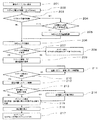
- FIG. 2 is a basic process flowchart up to sample analysis by the EBSD detector in the present embodiment. It is assumed that the sample has already been placed in the vacuum chamber 107. A sample position adjustment method in the charged particle beam apparatus described later can be executed by a computer program stored in the storage unit 122 connected to the control computer 118.
- FIG. 3 is a diagram showing a guide flow (overall operation flow).
- the user can easily analyze a desired sample position by performing an operation along this guide flow.
- the user designates a desired analysis position from the analysis area displayed on the image display device 117 using the operation input unit 121 in a state where the sample 102 is placed in the vacuum chamber 107 (step 301).
- a pseudo image is displayed based on the set position information of the stage 116, and it is confirmed whether the setting of the stage 116 is a desired analysis position or a pseudo image (step 303).
- the position (X axis, Y axis, R axis) can be finely adjusted by the operation input unit 121 (step 302).
- the detector 101 is inserted (step 304), and analysis by the EBSD detector 101 is started (step 305).
- the stage 116 can be easily adjusted in an EBSD analysis in a short time.
- the flow shown in FIG. 2 is a part of the flow shown in FIG. 3, and is a preparatory operation for setting the position of the sample.
- the Z axis of the stage 116 is automatically moved to a height of 20 mm (step 202).
- This height is a height at which the stage 116 and the aperture member do not come into contact with each other even when the stage 116 is tilted at a maximum of 70 degrees.
- step 203 the presence or absence of the CCD camera 119 image is confirmed. If the presence of the CCD camera 119 image is recognized, a confirmation as to whether the analysis is performed using the image obtained by the CCD camera 119 is displayed on the display device 117 (step 204). If a CCD image is used in step 204, an image of the sample used for analysis is acquired (step 205). At this time, it is desirable to obtain a planar image of the entire sample. Then, the process proceeds to Step 206. If it is determined in step 204 that no analysis area is designated from the CCD image, the process also proceeds to step 206.
- step 206 the area to be analyzed is designated.
- the analysis area is designated by an operator (user) using a pseudo image displayed on the display device 117.
- the pseudo image is generated by processing by the control computer 118 based on the information on the sample stage 103 set by the user. If a CCD image has been acquired in step 205, that image is used.
- step 206 a region that cannot be analyzed due to the inclination of the sample 102 is calculated on the acquired image, a pseudo image and a synthesis process are performed, and the synthesized image is displayed on the display device 117.
- FIG. 4 is an example of a composite image to be displayed.
- a stage movable range display 401 a stage movable range display 401, a hatched area display 402 for displaying an area that cannot be analyzed due to the stage tilt, and a display 403 outside the stage movable range are displayed as a composite image.
- the stage movable range 401 is displayed in consideration of the analysis range that is expanded when the stage 116 is rotated in advance. Thereby, since the analysis range to be expanded when the stage 116 is rotated can be known in advance, it is convenient and easy to use.
- the stage 116 when the stage 116 is tilted, normally, when the center of the rotation axis of the stage 116 and the irradiation axis of the charged particle beam 104 do not coincide with each other, the vicinity of the center of the stage 116 becomes an unanalysable region. Since this region takes into account the rotation of the stage 116, it has a circular shape.
- the composite image shown in FIG. 4 is displayed, it is possible to grasp in advance a region where analysis due to the inclination of the stage 116 is impossible, so it is not necessary to incline the stage 116 to check whether analysis is possible, and it is convenient and easy to use.
- the region that can be analyzed without knowing that the stage 116 is actually operated is known, the stage 116 and the aperture member do not come into contact with each other, which is safe.
- step 206 of FIG. 2 the expansion of the analysis possible range by the rotation of the R axis is also considered.
- the area where the analysis becomes impossible can be calculated from the size of the sample stage 103 being used and the tilt angle of the sample 102, the axis position of the rotation of the stage 116, and the irradiation position of the charged particle beam 104.
- the calculation of the area is performed by a calculation processing unit inside the control computer 118.
- a conversion table may be prepared in advance, or may be obtained each time by calculation using a conversion formula. Since the calculation can be performed with a simple conversion formula, the amount of calculation is small even if the calculation is performed each time.
- the user sets the position (X-axis direction, Y-axis direction) of the stage 116 with the operation input unit 121 while viewing the composite image displayed on the display device 117.
- the position (X-axis direction and Y-axis direction) of the stage 116 set by the user is determined by the arithmetic processing unit inside the control computer 118 as to whether the stage can be moved by combining the planar movement or rotational movement of the stage 116. (Step 207). If it is determined in step 207 that the stage 116 cannot be moved, guidance indicating that the stage cannot be moved to the set position is displayed on the display device 117, and the guide flow is terminated (step 208). In the example shown in FIG. 2, the guide flow is ended. However, the flow may be such that the analysis area can be designated again after displaying the guidance that cannot be set.
- an operation input unit a means for a user such as a mouse to perform input for instructing the state of the sample stage 103 and the analysis target portion
- the operation input unit includes a touch panel of the display device 117.
- step 207 if the stage can be moved, the sample stage 116 is set in accordance with the position (X-axis direction, Y-axis direction), rotation angle (R direction), and tilt angle (T direction) set by the user. Are displayed on the display device 117 (step 209).
- the user can confirm the movement of the sample by displaying the process in which the stage 116 operates (step 210).
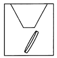
- FIG. 5 is an image showing the positional relationship between the sample stage 502 and the aperture member 501 of the stage 116 before tilting.
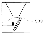
- FIG. 7 shows the positional relationship between the sample stage 502 of the stage 116 after tilting, the aperture member 501, and the inserted detector 503.
- the positional relationship between the sample stage 502 of the tilted stage 116 and the inserted detector 503 can be intuitively imaged. Since the accuracy of analysis is better when the sample and the EBSD detector 503 are as close as possible, if the image is displayed as shown in FIG. In addition, since the operator can intuitively imagine that the detector 503 is inserted, damage due to contact between the detector 503 and the sample due to an erroneous operation is eliminated, which is safe.
- the user finely adjusts the stage position (X-axis direction and Y-axis direction) and rotation angle (R-direction) while viewing the pseudo image. It can be adjusted (step 211). Also, the stage position (X-axis direction, Y-axis direction) and rotation angle (R-direction) can be adjusted by manipulating the state of the image of the sample stage represented in the pseudo-image, such as by dragging the pseudo-image directly with the mouse. If it can be set, the operability is further improved. Further, viewpoint switching, enlargement, and reduction may be possible. Further, if the display device 117 is a touch panel, it can be used instead of an operation using the operation input unit 121 such as a mouse.
- the stage 116 is moved to the stage position (X-axis direction, Y-axis direction), rotation angle (R direction), and tilt angle (T direction) set in step 210 (step 212).
- the pseudo image (FIG. 5) showing the positional relationship between the stage 116 and the aperture member when the stage 116 is viewed from the lateral direction (ZT direction) is accompanied by the movement of the tilt angle (T direction) of the stage 116.
- the stage is tilted gradually and displayed as shown in FIG.
- step 213 it is determined whether or not the infrared camera 120 capable of photographing the relationship between the stage 116 in the vacuum chamber 107 and the aperture member is installed.
- a captured image of the infrared camera may be displayed on the display device 117 (step 214).
- a mechanism for detecting whether or not the camera is mounted may be provided, and the camera mounting signal may be detected and switched automatically, or the display device 117 displays a confirmation of the use of the camera image. It may be switched by manual setting by a user operation.
- the tilt axis and the scanning direction differ depending on the relationship between the tilt direction of the stage 116 and the position of the detector 101. For this reason, the upper and lower sides of the sample 102 may not be in focus due to the distance between the electron gun 111 and the sample 102 being different. Therefore, in order to enable the clearest observation, the scanning direction is rotated by raster rotation, and the rotation is automatically performed so that the tilt axis direction and the scanning direction are parallel to each other.
- step 215 guidance indicating that the detector 101 can be inserted is displayed on the display device 117 (step 215).
- the insertion operation of the detector 101 is performed by a user operation based on the displayed guidance (step 216).
- the positional relationship between the stage 116, the aperture member, and the detector 101 is displayed as a pseudo image (FIG. 7).
- the pseudo image at this time may be replaced with a camera image as in step 213.
- the measurement preparation completion guidance of the EBSD detector 101 is displayed, and observation is started by scanning the sample with the primary charged particle beam 104 (step 217).
- analysis by the EBSD detector 101 is possible without being aware of the observation field escape of the sample due to the inclination of the stage 116 and the contact between the detector 101, the stage 116, and the aperture member. .
- the user can grasp in advance the movable range of the stage 116 from the pseudo image, there is no hassle of searching for a desired observation visual field, the observation of the desired position can be easily performed, and the charged particle beam apparatus and sample that are convenient and easy to use.
- a position adjustment method can be realized.
- the stage 116 and the aperture member do not come into contact with each other, which is safe.
- a part of the configuration of a certain embodiment can be replaced with the configuration of another embodiment, and the configuration of another embodiment can be added to the configuration of a certain embodiment. Further, it is possible to add, delete, and replace other configurations for a part of the configuration of each embodiment.
- Each of the above-described configurations, functions, processing units, processing means, and the like may be realized by hardware by designing a part or all of them with, for example, an integrated circuit.
- each of the above-described configurations, functions, and the like may be realized by software by interpreting and executing a program that realizes each function by the processor.
- Information such as programs, tables, and files for realizing each function can be stored in a recording device such as a memory, a hard disk, an SSD (Solid State Drive), or a recording medium such as an IC card, an SD card, or a DVD.
- control lines and information lines indicate what is considered necessary for the explanation, and not all the control lines and information lines on the product are necessarily shown. Actually, it may be considered that almost all the components are connected to each other.
- an arrow indicating the direction of the detector or the like may be displayed in accordance with the pseudo image.
Landscapes
- Chemical & Material Sciences (AREA)
- Analytical Chemistry (AREA)
- Analysing Materials By The Use Of Radiation (AREA)
Abstract
Description
Claims (25)
- 荷電粒子線を放出する荷電粒子源と、
前記荷電粒子線を試料に照射する荷電粒子光学系と、
前記荷電粒子線の照射によって試料表面から発生する後方散乱電子回折を検出するEBSD検出器と、
前記試料が配置される試料台を支持し、移動する試料ステージと、
前記試料における前記EBSD検出器により分析可能な部分と、分析不可能な部分とを区別して表示する画像表示部と、
前記EBSD検出器による分析位置が入力される操作入力部と、
前記操作入力部から入力された前記分析位置を前記EBSD検出器で分析できるように前記試料ステージの平面移動、傾斜移動、および回転移動を制御する制御部と、
を備えることを特徴とする荷電粒子線装置。 - 請求項1に記載の荷電粒子線装置において、
前記画像表示部は、前記試料ステージの傾斜移動により前記EBSD検出器で分析不可能な部分と、前記試料ステージの移動範囲外であるために前記EBSD検出器で分析不可能な部分とを区別して表示することを特徴とする荷電粒子線装置。 - 請求項1に記載の荷電粒子線装置において、
前記画像表示部は、前記操作入力部から入力された前記分析位置が前記EBSD検出器により分析不可能な部分である場合、前記EBSD検出器による分析が不可能である旨を表示することを特徴とする荷電粒子線装置。 - 請求項1に記載の荷電粒子線装置において、
前記画像表示部は、前記EBSD検出器で分析できるように前記試料ステージが移動した後、前記EBSD検出器が挿入可能である旨を表示することを特徴とする荷電粒子線装置。 - 請求項1に記載の荷電粒子線装置において、
前記試料を撮像する撮像装置を備え、
前記画像表示部は、前記撮像装置によって得られた画像に、前記分析可能な部分と前記分析不可能な部分とを合成して表示することを特徴とする荷電粒子線装置。 - 請求項1に記載の荷電粒子線装置において、
前記画像表示部は、前記操作入力部から入力された前記分析位置に従って、前記試料ステージを移動させた場合の疑似画像を、前記試料ステージの移動に先立って表示することを特徴とする荷電粒子線装置。 - 請求項6に記載の荷電粒子線装置において、
前記擬似画像には、前記荷電粒子線光学系、前記EBSD検出器、および前記試料台の位置関係が表示されることを特徴とする荷電粒子線装置。 - 請求項6に記載の荷電粒子線装置において、
前記操作入力部は、前記画像表示部に前記疑似画像が表示された後、前記分析位置を再調整できることを特徴とする荷電粒子線装置。 - 請求項6に記載の荷電粒子線装置において、
前記試料を撮像する撮像装置を備え、
前記画像表示部は、前記撮像装置によって得られた画像を前記擬似画像に合成して表示することを特徴とする荷電粒子線装置。 - 荷電粒子線を放出する荷電粒子源と、
前記荷電粒子線を試料に照射する荷電粒子光学系と、
前記荷電粒子線の照射によって試料表面から発生する後方散乱電子回折を検出するEBSD検出器と、
前記試料が配置される試料台を支持し、移動する試料ステージと、
前記EBSD検出器による分析位置が入力される操作入力部と、
前記操作入力部から入力された前記分析位置が前記EBSD検出器により分析可能な部分である場合、当該分析位置を前記EBSD検出器で分析できるように前記試料ステージの平面移動、傾斜移動、および回転移動を制御する制御部と、
前記操作入力部から入力された前記分析位置が前記EBSD検出器により分析不可能な部分である場合、前記EBSD検出器による分析が不可能である旨を表示する画像表示部と、
を備えることを特徴とする荷電粒子線装置。 - 請求項10に記載の荷電粒子線装置において、
前記画像表示部は、前記試料ステージの傾斜移動により前記EBSD検出器で分析不可能な部分と、前記試料ステージの移動範囲外であるために前記EBSD検出器で分析不可能な部分とを区別して表示することを特徴とする荷電粒子線装置。 - 請求項10に記載の荷電粒子線装置において、
前記画像表示部は、前記EBSD検出器で分析できるように前記試料ステージが移動した後、前記EBSD検出器が挿入可能である旨を表示することを特徴とする荷電粒子線装置。 - 請求項10に記載の荷電粒子線装置において、
前記試料を撮像する撮像装置を備え、
前記画像表示部は、前記撮像装置によって得られた画像に、前記分析可能な部分と前記分析不可能な部分とを合成して表示することを特徴とする荷電粒子線装置。 - 請求項10に記載の荷電粒子線装置において、
前記画像表示部は、前記操作入力部から入力された前記分析位置に従って、前記試料ステージを移動させた場合の疑似画像を、前記試料ステージの移動に先立って表示することを特徴とする荷電粒子線装置。 - 請求項14に記載の荷電粒子線装置において、
前記擬似画像には、前記荷電粒子線光学系、前記EBSD検出器、および前記試料台の位置関係が表示されることを特徴とする荷電粒子線装置。 - 請求項14に記載の荷電粒子線装置において、
前記操作入力部は、前記画像表示部に前記疑似画像が表示された後、前記分析位置を再調整できることを特徴とする荷電粒子線装置。 - 請求項14に記載の荷電粒子線装置において、
前記試料を撮像する撮像装置を備え、
前記画像表示部は、前記撮像装置によって得られた画像を前記擬似画像に合成して表示することを特徴とする荷電粒子線装置。 - 荷電粒子線装置へのEBSD検出器の取付けをガイドする荷電粒子線装置の制御方法であって、
制御部に、試料ステージに支持された試料台の大きさと、前記EBSD検出器使用時の前記試料ステージの傾斜角度と、前記試料ステージの平面移動、傾斜移動および回転移動の範囲とに基づいて、前記試料台に配置された試料において前記EBSD検出器により分析可能な部分と、分析不可能な部分とを演算させ、
前記制御部に、操作入力部から入力された前記EBSD検出器による分析位置が、前記分析可能な部分である場合、当該分析位置を前記EBSD検出器で分析できるように前記試料ステージの平面移動、傾斜移動、および回転移動を制御させ、
前記分析位置を前記EBSD検出器で分析できるように前記試料ステージが平面移動、傾斜移動、および回転移動した後、画像表示部に、前記EBSD検出器が挿入可能である旨を表示させることを特徴とする荷電粒子線装置の制御方法。 - 請求項18記載の荷電粒子線装置の制御方法において、
前記画像表示部に、前記試料において前記EBSD検出器により分析可能な部分と、分析不可能な部分とを区別して表示させることを特徴とする荷電粒子線装置の制御方法。 - 請求項19記載の荷電粒子線装置の制御方法において、
前記画像表示部に、前記試料ステージの傾斜移動により前記EBSD検出器で分析不可能な部分と、前記試料ステージの移動範囲外であるために前記EBSD検出器で分析不可能な部分とを区別して表示させることを特徴とする荷電粒子線装置の制御方法。 - 請求項18記載の荷電粒子線装置の制御方法において、
前記操作入力部から入力された前記分析位置が前記EBSD検出器により分析不可能な部分である場合、前記画像表示部に、前記EBSD検出器による分析が不可能である旨を表示することを特徴とする荷電粒子線装置の制御方法。 - 請求項18記載の荷電粒子線装置の制御方法において、
前記画像表示部に、撮像装置によって得られた画像に、前記分析可能な部分と前記分析不可能な部分とを合成して表示させることを特徴とする荷電粒子線装置の制御方法。 - 請求項18記載の荷電粒子線装置の制御方法において、
前記画像表示部に、前記操作入力部から入力された前記分析位置に従って、前記試料ステージを移動させた場合の疑似画像を、前記試料ステージの移動に先立って表示することを特徴とする荷電粒子線装置の制御方法。 - 請求項23記載の荷電粒子線装置の制御方法において、
前記擬似画像には、前記荷電粒子線光学系、前記EBSD検出器、および前記試料台の位置関係が表示されることを特徴とする荷電粒子線装置の制御方法。 - 請求項23記載の荷電粒子線装置の制御方法において、
前記画像表示部に前記疑似画像が表示された後、前記操作入力部から前記EBSD検出器による分析位置を再入力できることを特徴とする荷電粒子線装置の制御方法。
Priority Applications (3)
| Application Number | Priority Date | Filing Date | Title |
|---|---|---|---|
| DE112014002848.7T DE112014002848B4 (de) | 2013-07-23 | 2014-05-21 | Mit einem Strahl geladener Teilchen arbeitende Vorrichtung, die eine erleichterte Analyse einer gewünschten Position mit einem EBSD-Detektor ermöglicht, und Steuerverfahren dafür |
| CN201480038531.8A CN105359249B (zh) | 2013-07-23 | 2014-05-21 | 能够用ebsd检测器容易地分析所期望位置的带电粒子线装置以及其控制方法 |
| US14/905,170 US9741531B2 (en) | 2013-07-23 | 2014-05-21 | Charged particle beam device enabling facilitated EBSD detector analysis of desired position and control method thereof |
Applications Claiming Priority (2)
| Application Number | Priority Date | Filing Date | Title |
|---|---|---|---|
| JP2013-153091 | 2013-07-23 | ||
| JP2013153091A JP5464535B1 (ja) | 2013-07-23 | 2013-07-23 | Ebsd検出器で所望箇所を容易に分析できる荷電粒子線装置およびその制御方法 |
Publications (1)
| Publication Number | Publication Date |
|---|---|
| WO2015011975A1 true WO2015011975A1 (ja) | 2015-01-29 |
Family
ID=50619410
Family Applications (1)
| Application Number | Title | Priority Date | Filing Date |
|---|---|---|---|
| PCT/JP2014/063491 Ceased WO2015011975A1 (ja) | 2013-07-23 | 2014-05-21 | Ebsd検出器で所望箇所を容易に分析できる荷電粒子線装置およびその制御方法 |
Country Status (5)
| Country | Link |
|---|---|
| US (1) | US9741531B2 (ja) |
| JP (1) | JP5464535B1 (ja) |
| CN (1) | CN105359249B (ja) |
| DE (1) | DE112014002848B4 (ja) |
| WO (1) | WO2015011975A1 (ja) |
Families Citing this family (15)
| Publication number | Priority date | Publication date | Assignee | Title |
|---|---|---|---|---|
| JP5464535B1 (ja) * | 2013-07-23 | 2014-04-09 | 株式会社日立ハイテクノロジーズ | Ebsd検出器で所望箇所を容易に分析できる荷電粒子線装置およびその制御方法 |
| JP6360620B2 (ja) * | 2015-03-31 | 2018-07-18 | 株式会社日立ハイテクノロジーズ | 荷電粒子線装置、荷電粒子線装置のアライメント方法、アライメントプログラム、及び記憶媒体 |
| WO2017216941A1 (ja) * | 2016-06-17 | 2017-12-21 | 株式会社 日立ハイテクノロジーズ | 荷電粒子線装置 |
| JP6928943B2 (ja) * | 2017-03-28 | 2021-09-01 | 株式会社日立ハイテクサイエンス | 荷電粒子ビーム装置 |
| JP2018170166A (ja) * | 2017-03-30 | 2018-11-01 | 株式会社日立ハイテクノロジーズ | 荷電粒子線装置 |
| JP6775003B2 (ja) * | 2018-12-26 | 2020-10-28 | 株式会社日立ハイテク | 荷電粒子線装置 |
| WO2020012704A1 (ja) * | 2019-03-06 | 2020-01-16 | 株式会社日立ハイテクノロジーズ | プラズマ処理装置およびプラズマ処理方法、ecr高さモニタ |
| EP3770945B1 (en) * | 2019-07-26 | 2024-06-19 | Bruker Nano GmbH | Kikuchi diffraction detector |
| TWI872112B (zh) * | 2019-09-25 | 2025-02-11 | 日商日立高新技術科學股份有限公司 | 聚焦離子束裝置 |
| JP7472512B2 (ja) * | 2020-01-31 | 2024-04-23 | 株式会社島津製作所 | 分析装置および分析装置の制御方法 |
| CN113433149B (zh) * | 2021-05-26 | 2022-10-11 | 中国科学院金属研究所 | 一种实现ebsd系统跨尺度连续自动表征分析测试方法 |
| CN116297586B (zh) * | 2022-12-12 | 2026-04-03 | 上海美维科技有限公司 | 一种封装基板ebsd样品及其制备方法 |
| WO2024139049A1 (zh) * | 2022-12-27 | 2024-07-04 | 纳克微束(北京)有限公司 | 一种探测系统 |
| JP7681649B2 (ja) * | 2023-07-19 | 2025-05-22 | 日本電子株式会社 | 荷電粒子線装置及びカメラ画像表示方法 |
| CN121577658A (zh) * | 2025-12-23 | 2026-02-27 | 中国地质科学院矿产资源研究所 | 一种用于地质薄片的ebsd测试样品台及ebsd测试方法 |
Citations (3)
| Publication number | Priority date | Publication date | Assignee | Title |
|---|---|---|---|---|
| JPH1040849A (ja) * | 1996-07-22 | 1998-02-13 | Hitachi Ltd | 透過電子顕微鏡 |
| JP2007179929A (ja) * | 2005-12-28 | 2007-07-12 | Hitachi High-Technologies Corp | 荷電粒子線装置及び試料像表示方法 |
| JP2007200573A (ja) * | 2006-01-23 | 2007-08-09 | Hitachi High-Technologies Corp | 電子顕微鏡およびその制御方法 |
Family Cites Families (23)
| Publication number | Priority date | Publication date | Assignee | Title |
|---|---|---|---|---|
| JPH1125898A (ja) * | 1997-05-08 | 1999-01-29 | Hitachi Ltd | 電子顕微鏡の分解能評価方法および分解能評価用試料 |
| JP2000277044A (ja) | 1999-03-24 | 2000-10-06 | Hitachi Ltd | 走査電子顕微鏡 |
| JP5180428B2 (ja) * | 2005-06-21 | 2013-04-10 | 株式会社日立ハイテクノロジーズ | 走査型電子顕微鏡用撮像レシピ作成装置及びその方法並びに半導体パターンの形状評価装置 |
| JP2007277044A (ja) * | 2006-04-07 | 2007-10-25 | Sony Corp | ダイヤモンドライクカーボン膜の形成方法 |
| JP5410286B2 (ja) * | 2006-10-20 | 2014-02-05 | エフ・イ−・アイ・カンパニー | S/temのサンプルを作成する方法およびサンプル構造 |
| JP5873227B2 (ja) * | 2007-12-06 | 2016-03-01 | エフ・イ−・アイ・カンパニー | デコレーションを用いたスライス・アンド・ビュー |
| JP5530601B2 (ja) * | 2008-03-31 | 2014-06-25 | 株式会社日立ハイテクノロジーズ | 走査型電子顕微鏡を用いた回路パターンの寸法計測装置およびその方法 |
| DE102008035163B4 (de) * | 2008-07-28 | 2013-12-12 | Ellcie Industries Gmbh | Elektronenmikroskop |
| JP5205306B2 (ja) | 2009-02-27 | 2013-06-05 | 株式会社日立ハイテクノロジーズ | 走査型電子顕微鏡 |
| DE102009001910A1 (de) * | 2009-03-26 | 2010-09-30 | Carl Zeiss Nts Gmbh | Verfahren und Vorrichtung zur Erzeugung dreidimensionaler Bilddaten |
| JP4926208B2 (ja) * | 2009-05-26 | 2012-05-09 | 株式会社日立ハイテクノロジーズ | 走査型電子顕微鏡装置、及び評価ポイント生成方法、並びにプログラム |
| JP5350123B2 (ja) * | 2009-08-10 | 2013-11-27 | 株式会社日立ハイテクノロジーズ | 荷電粒子線装置及び画像表示方法 |
| JP5517790B2 (ja) * | 2010-07-02 | 2014-06-11 | 株式会社キーエンス | 拡大観察装置 |
| EP2612342B1 (en) * | 2010-08-31 | 2018-08-22 | FEI Company | Navigation and sample processing using an ion source containing both low-mass and high-mass species |
| EP2450936B1 (en) * | 2010-11-03 | 2013-03-13 | Carl Zeiss NTS Ltd. | Microscope system, method for operating a charged-particle microscope |
| CN103403520B (zh) * | 2011-01-28 | 2015-12-23 | Fei公司 | Tem样品制备 |
| JP6215202B2 (ja) * | 2011-08-05 | 2017-10-18 | パルセータ, エルエルシーPulsetor, Llc | 密接に結合したシンチレータ−光電子増倍管の1又は複数の組合体を含む電子検出器及びそれを使用した電子顕微鏡 |
| WO2013192608A1 (en) * | 2012-06-22 | 2013-12-27 | Edax, Inc. | Method and apparatus for electron pattern imaging |
| US8502172B1 (en) * | 2012-06-26 | 2013-08-06 | Fei Company | Three dimensional fiducial |
| JP6261178B2 (ja) * | 2013-03-27 | 2018-01-17 | 株式会社日立ハイテクサイエンス | 荷電粒子ビーム装置、荷電粒子ビーム装置を用いた試料の加工方法、及び荷電粒子ビーム装置を用いた試料の加工コンピュータプログラム |
| JP2014225735A (ja) * | 2013-05-15 | 2014-12-04 | 日本電子株式会社 | 画像処理方法、画像処理装置、撮像装置、およびプログラム |
| JP5464535B1 (ja) * | 2013-07-23 | 2014-04-09 | 株式会社日立ハイテクノロジーズ | Ebsd検出器で所望箇所を容易に分析できる荷電粒子線装置およびその制御方法 |
| DE102014220122B9 (de) * | 2014-10-03 | 2019-11-21 | Carl Zeiss Microscopy Gmbh | Verfahren zum Messen eines Abstands eines Bauteils zu einem Objekt sowie zum Einstellen einer Position eines Bauteils in einem Teilchenstrahlgerät, Computerprogrammprodukt, Teilchenstrahlgerät sowie Gaszuführungseinrichtung |
-
2013
- 2013-07-23 JP JP2013153091A patent/JP5464535B1/ja active Active
-
2014
- 2014-05-21 US US14/905,170 patent/US9741531B2/en active Active
- 2014-05-21 WO PCT/JP2014/063491 patent/WO2015011975A1/ja not_active Ceased
- 2014-05-21 CN CN201480038531.8A patent/CN105359249B/zh active Active
- 2014-05-21 DE DE112014002848.7T patent/DE112014002848B4/de active Active
Patent Citations (3)
| Publication number | Priority date | Publication date | Assignee | Title |
|---|---|---|---|---|
| JPH1040849A (ja) * | 1996-07-22 | 1998-02-13 | Hitachi Ltd | 透過電子顕微鏡 |
| JP2007179929A (ja) * | 2005-12-28 | 2007-07-12 | Hitachi High-Technologies Corp | 荷電粒子線装置及び試料像表示方法 |
| JP2007200573A (ja) * | 2006-01-23 | 2007-08-09 | Hitachi High-Technologies Corp | 電子顕微鏡およびその制御方法 |
Also Published As
| Publication number | Publication date |
|---|---|
| CN105359249A (zh) | 2016-02-24 |
| DE112014002848B4 (de) | 2020-10-01 |
| CN105359249B (zh) | 2017-03-29 |
| JP2015023005A (ja) | 2015-02-02 |
| US20160163504A1 (en) | 2016-06-09 |
| DE112014002848T5 (de) | 2016-04-28 |
| JP5464535B1 (ja) | 2014-04-09 |
| US9741531B2 (en) | 2017-08-22 |
Similar Documents
| Publication | Publication Date | Title |
|---|---|---|
| JP5464535B1 (ja) | Ebsd検出器で所望箇所を容易に分析できる荷電粒子線装置およびその制御方法 | |
| CN104364877B (zh) | 带电粒子束装置 | |
| KR102496895B1 (ko) | 시료 위치 맞춤 방법 및 하전 입자 빔 장치 | |
| JP7367215B2 (ja) | 荷電粒子線装置、およびそのフォーカス調整方法 | |
| US12169182B2 (en) | Charged particle beam apparatus | |
| JP7061192B2 (ja) | 荷電粒子線装置 | |
| JP6360620B2 (ja) | 荷電粒子線装置、荷電粒子線装置のアライメント方法、アライメントプログラム、及び記憶媒体 | |
| CN111243928B (zh) | 用于检查标本的带电粒子显微镜和确定所述带电粒子显微镜的像差的方法 | |
| JP6764953B2 (ja) | 荷電粒子線装置 | |
| JPWO2016157403A6 (ja) | 荷電粒子線装置、荷電粒子線装置のアライメント方法、アライメントプログラム、及び記憶媒体 | |
| JP5491817B2 (ja) | 電子顕微鏡における薄膜試料位置認識装置 | |
| JP6775003B2 (ja) | 荷電粒子線装置 | |
| JP7059402B2 (ja) | 荷電粒子線装置及びその制御方法 | |
| JP6706956B2 (ja) | 分析装置 |
Legal Events
| Date | Code | Title | Description |
|---|---|---|---|
| WWE | Wipo information: entry into national phase |
Ref document number: 201480038531.8 Country of ref document: CN |
|
| 121 | Ep: the epo has been informed by wipo that ep was designated in this application |
Ref document number: 14829369 Country of ref document: EP Kind code of ref document: A1 |
|
| WWE | Wipo information: entry into national phase |
Ref document number: 112014002848 Country of ref document: DE |
|
| WWE | Wipo information: entry into national phase |
Ref document number: 14905170 Country of ref document: US |
|
| 122 | Ep: pct application non-entry in european phase |
Ref document number: 14829369 Country of ref document: EP Kind code of ref document: A1 |