WO2015011845A1 - 層間光波結合デバイス - Google Patents
層間光波結合デバイス Download PDFInfo
- Publication number
- WO2015011845A1 WO2015011845A1 PCT/JP2013/077037 JP2013077037W WO2015011845A1 WO 2015011845 A1 WO2015011845 A1 WO 2015011845A1 JP 2013077037 W JP2013077037 W JP 2013077037W WO 2015011845 A1 WO2015011845 A1 WO 2015011845A1
- Authority
- WO
- WIPO (PCT)
- Prior art keywords
- core
- coupling device
- interlayer
- substrate
- lightwave
- Prior art date
- Legal status (The legal status is an assumption and is not a legal conclusion. Google has not performed a legal analysis and makes no representation as to the accuracy of the status listed.)
- Ceased
Links
Images


Classifications
-
- G—PHYSICS
- G02—OPTICS
- G02B—OPTICAL ELEMENTS, SYSTEMS OR APPARATUS
- G02B6/00—Light guides; Structural details of arrangements comprising light guides and other optical elements, e.g. couplings
- G02B6/10—Light guides; Structural details of arrangements comprising light guides and other optical elements, e.g. couplings of the optical waveguide type
- G02B6/12—Light guides; Structural details of arrangements comprising light guides and other optical elements, e.g. couplings of the optical waveguide type of the integrated circuit kind
- G02B6/12002—Three-dimensional structures
-
- G—PHYSICS
- G02—OPTICS
- G02B—OPTICAL ELEMENTS, SYSTEMS OR APPARATUS
- G02B6/00—Light guides; Structural details of arrangements comprising light guides and other optical elements, e.g. couplings
- G02B6/10—Light guides; Structural details of arrangements comprising light guides and other optical elements, e.g. couplings of the optical waveguide type
- G02B6/12—Light guides; Structural details of arrangements comprising light guides and other optical elements, e.g. couplings of the optical waveguide type of the integrated circuit kind
- G02B6/122—Basic optical elements, e.g. light-guiding paths
- G02B6/1228—Tapered waveguides, e.g. integrated spot-size transformers
-
- G—PHYSICS
- G02—OPTICS
- G02B—OPTICAL ELEMENTS, SYSTEMS OR APPARATUS
- G02B6/00—Light guides; Structural details of arrangements comprising light guides and other optical elements, e.g. couplings
- G02B6/10—Light guides; Structural details of arrangements comprising light guides and other optical elements, e.g. couplings of the optical waveguide type
- G02B6/12—Light guides; Structural details of arrangements comprising light guides and other optical elements, e.g. couplings of the optical waveguide type of the integrated circuit kind
- G02B2006/12035—Materials
- G02B2006/12038—Glass (SiO2 based materials)
-
- G—PHYSICS
- G02—OPTICS
- G02B—OPTICAL ELEMENTS, SYSTEMS OR APPARATUS
- G02B6/00—Light guides; Structural details of arrangements comprising light guides and other optical elements, e.g. couplings
- G02B6/10—Light guides; Structural details of arrangements comprising light guides and other optical elements, e.g. couplings of the optical waveguide type
- G02B6/12—Light guides; Structural details of arrangements comprising light guides and other optical elements, e.g. couplings of the optical waveguide type of the integrated circuit kind
- G02B2006/12035—Materials
- G02B2006/12061—Silicon
-
- G—PHYSICS
- G02—OPTICS
- G02B—OPTICAL ELEMENTS, SYSTEMS OR APPARATUS
- G02B6/00—Light guides; Structural details of arrangements comprising light guides and other optical elements, e.g. couplings
- G02B6/10—Light guides; Structural details of arrangements comprising light guides and other optical elements, e.g. couplings of the optical waveguide type
- G02B6/12—Light guides; Structural details of arrangements comprising light guides and other optical elements, e.g. couplings of the optical waveguide type of the integrated circuit kind
- G02B2006/12035—Materials
- G02B2006/12069—Organic material
- G02B2006/12073—Epoxy
-
- G—PHYSICS
- G02—OPTICS
- G02B—OPTICAL ELEMENTS, SYSTEMS OR APPARATUS
- G02B6/00—Light guides; Structural details of arrangements comprising light guides and other optical elements, e.g. couplings
- G02B6/10—Light guides; Structural details of arrangements comprising light guides and other optical elements, e.g. couplings of the optical waveguide type
- G02B6/12—Light guides; Structural details of arrangements comprising light guides and other optical elements, e.g. couplings of the optical waveguide type of the integrated circuit kind
- G02B2006/12083—Constructional arrangements
- G02B2006/12095—Graded
-
- G—PHYSICS
- G02—OPTICS
- G02B—OPTICAL ELEMENTS, SYSTEMS OR APPARATUS
- G02B6/00—Light guides; Structural details of arrangements comprising light guides and other optical elements, e.g. couplings
- G02B6/10—Light guides; Structural details of arrangements comprising light guides and other optical elements, e.g. couplings of the optical waveguide type
- G02B6/12—Light guides; Structural details of arrangements comprising light guides and other optical elements, e.g. couplings of the optical waveguide type of the integrated circuit kind
- G02B2006/12133—Functions
- G02B2006/12147—Coupler
Definitions
- the present invention relates to interlayer lightwave coupling devices.
- the three-dimensional optical interconnection technology has not only an increase in bandwidth but also has the advantage of being able to realize optical waveguide crossing with low loss and less leakage. This is because two intersecting optical waveguides can be spatially separated.
- the importance of high performance, superior optical waveguide crossing is dramatically increasing with the increasing density and complexity of optical interconnects.
- To realize a three-dimensional optical interconnection low loss optical coupling between two different optical interconnection layers is essential, but this realization is not easy. The reason is that light is different from the case of electricity, and a large light loss is generated due to a sharp bend of a transmission path or a discontinuity of refractive index. Therefore, the following techniques have been proposed for exchanging light waves between layers.
- FIG. 7 by combining a plurality of spot size converters having a tapered structure mainly used for connection of optical signals between a chip and an optical fiber, light is generated between optical waveguides respectively disposed in different layers. Methods have been proposed to couple signals together.
- (a) is a perspective view of the interlayer optical wave coupling device
- (b) is a schematic plan view thereof
- (c) is a schematic central cross-sectional view thereof. Because the optical waveguides arranged in the upper and lower layers have a tapered structure, even if there is a structural or material difference in refractive index between the optical waveguides, the optical waveguide may be located anywhere on the tapered structure.
- the mode shape of the light wave can be widely expanded to the outside of the optical waveguide, so that the light waves are coupled in principle even if the interlayer distance is sufficiently separated
- the light wave is easily dissipated from the optical waveguide due to a slight perturbation of the optical waveguide structure which is generated unintentionally, which causes loss. That is, although this method has high efficiency, there is a problem that it is difficult to sufficiently separate the layers.
- Non-Patent Document 4 There is also a method of changing the direction of light propagation by placing a mirror in the optical waveguide, directing the light to different layers, and guiding the light to the optical waveguide of the different layer by using a similar mirror. .
- the formation of a mirror surface having a high reflectance is very difficult, and in particular, since silicon has a high refractive index, mirror surface formation is more difficult.
- the alignment tolerance of the mirror surface between the upper and lower layers is small, and high manufacturing accuracy is required. (See Non-Patent Document 4)
- Non-Patent Document 1 The prior art described in Non-Patent Document 1 is not sufficient in the following points. (1) Do not separate the interlayer distance sufficiently. Moreover, the prior arts described in Patent Document 1 and Non-Patent Documents 2 and 3 are not sufficient in the following points. (2) In principle, the coupling efficiency is low. (3) There is very large wavelength dependence and polarization dependence in coupling efficiency. (4) The grating couplers in the upper and lower layers must be arranged with high alignment accuracy. Furthermore, the prior art described in Non-Patent Document 4 is not sufficient in the following points. (5) It is difficult to form a mirror surface of a mirror and to realize highly efficient light wave coupling. (6) The mirror surfaces of the upper and lower layers must be arranged with high alignment accuracy.
- the present invention has been proposed in view of the above points (1) to (6), and light waves propagating in the light wave circuit between different light wave circuit layers are polarized in both the pseudo TE mode and the pseudo TM mode. It is an object of the present invention to provide an interlayer lightwave coupling device capable of efficiently coupling and capable of sufficiently suppressing deterioration of coupling efficiency due to structural and material variations caused by manufacturing and the like.
- At least two cores having a pointed structure on a substrate are spatially separated via another core having a smaller refractive index than the two cores, and the pointed structures of the two cores are: An interlayer lightwave coupling device characterized in that it is arranged so as to have no overlap in plan view.
- An interlayer lightwave coupling device wherein the structure and the second sharp structure are arranged so as not to have an overlap in plan view.
- FIG. 1 is a plan view schematically showing a basic structure of an interlayer lightwave coupling device according to the present invention. It is a center cross-sectional schematic diagram which shows the basic structure of the interlayer optical coupling device which concerns on this invention.
- FIG. 2 is a left side schematic view showing the basic structure of the interlayer lightwave coupling device according to the present invention.
- FIG. 1 is a right side schematic view showing a basic structure of an interlayer lightwave coupling device according to the present invention.
- 1 is a perspective view of an embodiment of an interlayer lightwave coupling device according to the present invention.
- 1 is a central cross-sectional schematic view of an embodiment of the interlayer lightwave coupling device according to the present invention. It is a schematic diagram which shows the structure of the conventional interlayer lightwave coupled device.
- FIG. 1 to 4 are schematic views showing the basic structure of the interlayer lightwave coupling device according to the present invention.
- FIG. 1 is a schematic plan view thereof
- FIG. 2 is a schematic central cross-sectional view thereof.
- FIG. 3 is the left side schematic diagram
- FIG. 4 is the right side schematic diagram.
- FIGS. 1 to 4 The basic structure of the interlayer lightwave coupling device according to the present invention shown in FIGS. 1 to 4 is as follows.
- a first optical waveguide formed on a substrate such as an SOI (Silicon On Insulator) substrate and a third optical waveguide in the upper layer are light-wave coupled via a second optical waveguide.
- the longitudinal directions of the first and second sharpened structures are schematically shown in a reduced size than in actuality.
- the basic structure of the above-described interlayer lightwave coupling device is such that the substrate, the first core of the first optical waveguide having the first pointed structure disposed on the substrate, and the first core are spatially separated.
- the third core of the third optical waveguide having the second sharpened structure is interposed between the first core and the third core and has a smaller refractive index than the first and third cores. It consists of the 2nd core used as a 2nd optical waveguide.
- the first sharpening structure and the second sharpening structure are spatially separated and arranged so as to have no overlap in plan view. .
- the light waves propagating in the first optical waveguide or the third optical waveguide are coupled to the second optical waveguide by passing through the respective pointed portions. After that, the lightwave propagating in the second optical waveguide is coupled to the third optical waveguide or the first optical waveguide disposed in different lightwave circuit layers by passing through the location of the pointed structure.
- the coupling efficiency of the lightwave to the second optical waveguide does not depend on the size of the core of the second optical waveguide, as long as using an appropriate sharp structure. Since the height of the core of the second optical waveguide corresponds to the distance between the layers, the distance between the layers can be increased by increasing the core size of the second optical waveguide. In addition, since a continuous structure is used, the light wave coupling efficiency between the layers is extremely high in principle and the wavelength dependency is extremely small in principle when an appropriately long pointed structure is used.
- the core structure at the tip of the optical waveguide forms an acute angle as a sharp structure.
- a structure in which the tip of the core forms an acute-angled isosceles triangle in plan view is a representative example.
- the inventors of the present invention have proposed a method capable of producing a sharp structure of an optical waveguide equivalently by an electron beam exposure technique or an immersion excimer stepper technique even with a stepper with a low resolution such as an i-line stepper.
- a method capable of producing a sharp structure of an optical waveguide equivalently by an electron beam exposure technique or an immersion excimer stepper technique even with a stepper with a low resolution such as an i-line stepper See Patent Document 2
- an acute-angled isosceles triangle in which each side of the tip of the core is removed equally and diagonally as an acute-angled structure, or one in which only one side of the tip of the core is removed obliquely to obtain an acute triangle It can be made.
- the present inventors have proposed a sharpened structure in which inclined side walls are formed on the side of the tip of the core, a sharpened structure having a thickness reduced toward the tip, and a method of manufacturing the same. .
- Patent Document 3 and Non-Patent Documents 5 and 6 According to this, the following modified example can be mentioned as a further sharp structure.
- the inclination angle of the side wall is preferably 60 degrees or more and 85 degrees or less. Furthermore, 75 degrees or more and 80 degrees or less are more preferable.
- the angle of inclination of each side does not have to be the same.
- a pointed structure in which the cross-sectional shape in the vicinity of the tip is a triangle like a knife edge.
- the sharp structure of the above (1) to (4) has the double patterning technique disclosed in Patent Document 2 and the inclination of the core in which the lower part is expanded compared to the upper part of the side wall disclosed in Patent Documents 3 and Non-patent Documents 5 to 6.
- This can be realized by appropriately combining dry etching techniques capable of forming a structure.
- the need for a width of 100 nm or less is pointed out for the pseudo TE mode in order to realize low loss light wave coupling, and for the pseudo TM mode, A tip having a width of 50 nm or less is desired.
- the polarization dependence of the lightwave coupling efficiency between the layers can be reduced by using the sharpened structure in which the tip of the core is narrowed.
- the sharp structure of the above (1) to (4) can maintain the width of 50 nm or less without breaking its tip in its cross-sectional structure, so that only the pseudo TE mode of the light wave coupling efficiency between layers
- the polarization dependence can be significantly reduced also for the pseudo TM mode.
- all the first pointed structures included in at least the first optical waveguide are contained in the second optical waveguide, and the third optical waveguide includes the third. All of the bottom surfaces of the two pointed structures may be in contact with the top surface of the second optical waveguide. Therefore, by increasing the width and length of the second optical waveguide, it is not necessary to make the two sharp structures face each other under extremely strict conditions, and the manufacturing cost can be reduced.
- the structural feature that the thickness (height) of the sharp structure is reduced has the physical-optical advantage of the light mode as well as the structural mechanical advantage. That is, as the thickness decreases, penetration of light intensity in the quasi-TM mode near the tip into the second waveguide core from the silicon optical waveguide becomes more effective, and as a result, the quasi-TM mode Mode conversion loss can be effectively reduced. Because of this, it is possible to reduce the polarization dependence of the mode conversion loss.
- the sidewall inclination etching process for producing the sharp structure of the above (1) to (4) is widely used in the back end process (BEOL) for forming the metal wiring of LSI formed on an optical integrated circuit substrate or the like. It is potentially highly compatible with BEOL, as it can be done by the i-line exposure method used. Therefore, cost reduction of an optical integrated circuit having an optical wiring network based on hydrogenated amorphous silicon which has high transparency and can be grown at low temperature and is stacked on a metal wiring layer of LSI can be expected.
- BEOL back end process
- FIG. 5 shows a perspective view of an embodiment of the interlayer lightwave coupling device according to the present invention.
- a first optical waveguide having a sharp edge structure also referred to as a knife edge structure
- a first core is formed.
- the third core of the third optical waveguide also has the same shape as the first core, and is spatially separated from the first core and disposed so as to have no overlap in plan view .
- a second core of a second optical waveguide having a smaller refractive index than the first core and the third core is interposed between the first core and the third core.
- the material of the first core and the third core is preferably silicon in view of the refractive index and the like.
- the silicon material is not limited to crystalline silicon, and may be polysilicon or amorphous silicon. In the case of amorphous silicon, in order to reduce the absorption loss of the material, hydrogenated amorphous silicon is preferable, but a material in which carbon, germanium or the like is added in addition to the silicon element may be used.
- the material of the second core is preferably SiON, SiO x , SiN, SiC, GaAs, or InP. Furthermore, an upper clad made of epoxy resin or SiO 2 is formed to cover the second core and the third core.
- an SOI (Silicon On Insulator) substrate, an optical integrated circuit substrate or the like is used as a substrate for the lightwave coupling device in FIG. 5.
- the center cross section schematic diagram is shown in FIG.
- the cross-sectional shapes and positional relationships of the first to third cores of the first to third optical waveguides and the first and second pointed structures are as illustrated.
- the first core of the first optical waveguide and the third core of the third optical waveguide are spatially separated in FIG. 6 through the second core of the second optical waveguide having a thickness of 1.0 ⁇ m. It is done.
- the thickness of the second optical waveguide may be any thickness as long as it is thicker than the thickness of the first optical waveguide.
- the first pointed structure of the first core and the second pointed structure of the third core are spatially separated by about 100 ⁇ m.
- an upper cladding is formed to cover the second core of the second optical waveguide and the third core of the third optical waveguide.
- interlayer lightwave coupling device of the present invention has been described with reference to the basic structure and the embodiment illustrated in FIGS. 1 to 6, these are for the purpose of facilitating the understanding of the interlayer lightwave coupling device of the present invention. It is a thing. Therefore, modifications and other embodiments based on the technical idea of the present invention described in the claims are naturally included in the interlayer light wave coupling device of the present invention.
- each side of the sharp structure of the first core and the third core in the basic structure and the embodiment illustrated in FIGS. 1 to 6 has a linear shape in plan view, but has a concave shape or a convex shape.
- at least one of the first core, the second core, and the third core may be a graded index waveguide or a step index waveguide. In this case, it is necessary that the effective refractive index when the first optical waveguide and the third optical waveguide exist alone is larger than that of the second optical waveguide.
Landscapes
- Physics & Mathematics (AREA)
- Engineering & Computer Science (AREA)
- Microelectronics & Electronic Packaging (AREA)
- General Physics & Mathematics (AREA)
- Optics & Photonics (AREA)
- Power Engineering (AREA)
- Optical Integrated Circuits (AREA)
Abstract
Description
三次元光配線を実現するためには、異なる二つの光配線層間での低損失な光結合が不可欠であるが、この実現は容易ではない。なぜならば、光は電気の場合と異なり、急激な伝送路の屈曲や屈折率の不連続によって大きな光損失が発生してしまうためである。そのため、層間で光波をやり取りする際には、以下のような技術が提案されている。
図7において、(a)は層間光波結合デバイスの斜視図、(b)はその平面模式図、(c)はその中央横断面模式図である。
上下層に配置されている光導波路が互いにテーパ構造を有しているために、互いの光導波路に構造的あるいは材料的な屈折率の差異が存在したとしても、テーパ構造のどこかで、上下層の光導波路がそれぞれ単独で存在した場合の実効屈折率が上下層で一致する箇所が存在する。そのため、構造的あるいは材料的な屈折率の変動に対して鈍感な光波結合を実現できる。加えて、光波結合を利用しているために原理的に低損失であり、しかも光波の上下層間の結合箇所は一箇所のみであるため、一度光波が移行した後は再び元の光導波路へ光波が戻ることはほとんどない。
すなわち、この方法は、効率は高いものの、層間の間隔を十分に離すことが困難であるといった問題がある。
しかしながらこの方法では、原理的に低い効率、大きな波長依存性、大きな偏波面依存性、上下層に配置されるミラー面を高い位置合わせ精度を持って配置しなければならないなどの問題がある。
しかし、高い反射率を有する鏡面の形成は非常に困難であり、特にシリコンは屈折率が高いために、鏡面形成がより一段と困難である。
さらに、上下層間のミラー面の位置合わせトレランスが小さく、高い製造精度を必要とする。(非特許文献4参照)
(1)層間距離を十分離せないこと。
また、特許文献1並びに非特許文献2、3に記載の先行技術は、次の点で十分でなかった。
(2)原理的に結合効率が低いこと。
(3)結合効率に非常に大きな波長依存性並びに偏波依存性が存在すること。
(4)上下層のグレーティング結合器を高い位置合わせ精度で配置しなければならないこと。
さらに、非特許文献4に記載の先行技術は、次の点で十分でなかった。
(5)ミラーの鏡面形成が困難であり、高効率な光波結合の実現が困難であること。
(6)上下層のミラー面を高い位置合わせ精度で配置しなければならないこと。
(1)基板上に先鋭構造を有する少なくとも二個のコアが該二個のコアよりも屈折率が小さい他のコアを介して空間的に離隔するとともに、該二個のコアの先鋭構造は、平面視して重なりを持たないように配置されていることを特徴とする層間光波結合デバイス。
(2)基板と、該基板上に配置され第一の先鋭構造を有する第一のコアと、該第一のコアとは空間的に離隔して配置され第二の先鋭構造を有する第三のコアと、該第一のコアと該第三のコアとの間に介在し該第一のコア及び第三のコアよりも屈折率が小さい第二のコアとを備えるとともに、該第一の先鋭構造及び該第二の先鋭構造は、平面視して重なりを持たないように配置されていることを特徴とする層間光波結合デバイス。
(3)上記第一のコア、上記第二のコア及び上記第三のコアがステップ屈折率導波路あるいはグレーデッド屈折率導波路であることを特徴とする(2)に記載の層間光波結合デバイス。
(4)上記基板上に、上記第二のコア及び上記第三のコアを覆うクラッドをさらに備えたことを特徴とする(2)又は(3)に記載の層間光波結合デバイス。
(5)上記第一のコア及び第三のコアは、シリコンからなることを特徴とする(2)ないし(4)のいずれかに記載の層間光波結合デバイス。
(6)上記第二のコアは、SiON、SiOX、SiN、SiC、GaAs及びInPのいずれかからなることを特徴とする(2)ないし(5)のいずれかに記載の層間光波結合デバイス。
(7)上記クラッドは、エポキシ樹脂又はSiO2のいずれかからなることを特徴とする(4)ないし(6)のいずれかに記載の層間光波結合デバイス。
(8)上記先鋭構造は、少なくとも一辺に傾斜した側壁を有することを特徴とする(1)ないし(7)のいずれかに記載の層間光波結合デバイス。
(9)上記先鋭構造を構成する一辺及び他の一辺の双方が、傾斜した側壁を有することを特徴とする(1)ないし(8)のいずれかに記載の層間光波結合デバイス。
(10)上記先鋭構造は、先端に向かって厚みが減少していることを特徴とする(1)ないし(9)のいずれかに記載の層間光波結合デバイス。
(11)上記先鋭構造の先端付近の断面形状が三角形であることを特徴とする(10)に記載の層間光波結合デバイス。
(12)上記基板は、SOI基板であることを特徴とする(1)ないし(11)のいずれかに記載の層間光波結合デバイス。
(13)上記基板は、光集積回路基板であることを特徴とする(1)ないし(11)のいずれかに記載の層間光波結合デバイス。
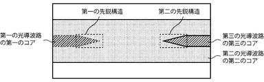
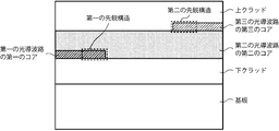
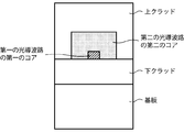
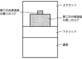
図1ないし図4は、本発明に係る層間光波結合デバイスの基本構造を示す模式図である。
図1は、その平面模式図であり、図2は、その中央横断面模式図である。また、図3は、その左側面模式図であり、図4は、その右側面模式図である。
SOI(Silicon On Insulator)基板等の基板上に形成された第一の光導波路と上層の第三の光導波路とは、第二の光導波路を介して光波結合される。
なお、図1ないし図2において、第一及び第二の先鋭構造の長さ方向は、実際より縮小して模式的に図示している。
さらに、図1ないし図4から分かるように、第一の先鋭構造及び第二の先鋭構造は、空間的に離隔して配置されるとともに、平面視して重なりを持たないように配置されている。
第一の光導波路又は第三の光導波路中を伝搬している光波は、それぞれの先鋭構造の箇所を通過することで、第二の光導波路へと結合する。その後、第二の光導波路中を伝搬している光波は、異なる光波回路層に配置されている第三の光導波路あるいは第一の光導波路へ、先鋭構造の箇所を通過することで結合する。
また、連続的な構造を用いていることから、適切な横長の先鋭構造を用いた場合、原理的に層間での光波結合効率は非常に高く、波長依存性はきわめて小さい。
本発明では、光導波路の先端部のコアの構造が鋭角を構成するものを先鋭構造とする。図1から分かるように、コアの先端が平面視して鋭角の二等辺三角形を構成する構造が代表例である。
この方法によれば、先鋭構造として、コアの先端の各辺を均等に斜めに除去した鋭角の二等辺三角形やコアの先端の一辺のみを斜めに除去して鋭角の三角形としたものを精度良く作製することができる。
これによれば、さらに先鋭構造として次のような変形例があげられる。
(1)一辺に傾斜した側壁を有する先鋭構造。
側壁の傾斜角度は、60度以上85度以下が好ましい。さらに、75度以上80度以下がより好ましい。
(2)一辺及び他の一辺の双方が、傾斜した側壁を有する先鋭構造。
側壁の傾斜角度は、上記(1)に準ずる。各辺の傾斜角度は必ずしも同一である必要はない。
(3)先端に向かって厚み(高さ)が減少している先鋭構造。
(4)上記(2)及び(3)の構造を組み合わせることにより、ナイフエッジのように先端付近の断面形状を三角形とした先鋭構造。
例えば、先鋭構造における側壁の傾斜構造は、シリコンにアンダーカットの入るガス、SF6と、側壁の保護膜を堆積させることのできるガス、例えばC4F8との混合ガス雰囲気中で誘導結合型反応性イオンエッチング行い、その混合比R(=SF6/C4F8)を調整することで適宜傾斜角度を制御することにより実現することができる。
本発明に係る層間光波結合デバイスでは、コアの先端が細くなった先鋭構造を用いることによって、層間での光波結合効率の偏波依存性を減少させることができる。
特に上記(1)ないし(4)の先鋭構造は、その断面構造上その先端が壊れることがなく50nm以下の幅を維持することができるため、層間での光波結合効率の、擬TEモードのみならず擬TMモードに対しても偏波依存性を顕著に減少させることができる。
したがって、第二の光導波路の幅及び長さを大きくとることにより、二つの先鋭構造を構造的にきわめて厳しい条件で対向させる必要がなくなり、製造コストを下げることができる。
これにより二つの先鋭構造の配置の範囲があらゆる方向に関して広がる。これは設計の自由度を上げるのみならず、製造精度を低くし製造コストを下げる効果がある。
すなわち、厚みが減少することで、先端付近での擬TMモードにおける光強度のシリコン光導波路中から第二導波路コア中への浸み出しがより効果的になり、その結果として、擬TMモードに対するモード変換損失を効率的に減少させることができる。このために、モード変換損失の偏波依存性を減少させることができる。
このため、LSIの金属配線層上に積層される、高い透過性を有し低温成長可能な水素化アモルファスシリコンに基づいた光配線ネットワークを有する光集積回路の低コスト化が期待できる。
図5に、本発明に係る層間光波結合デバイスの一実施形態の斜視図を示す。図5から分かるように、基板上に形成された下クラッド上に、傾斜した側壁を備え、先端付近の断面形状を三角形とした先鋭構造(ナイフエッジ構造ともいう)を有する第一の光導波路の第一のコアが形成されている。
第三の光導波路の第三のコアも第一のコアと同様の形状を有し、第一のコアとは空間的に離隔するとともに、平面視して重なりを持たないように配置されている。
第一のコアと第三のコアとの間には、第一のコア及び第三のコアよりも屈折率が小さい第二の光導波路の第二のコアが介在している。
シリコン材料としては、結晶シリコンに限らずポリシリコンやアモルファスシリコンでもよい。アモルファスシリコンの場合、材料の吸収損失を低減化するために、水素化アモルファスシリコンが好ましいが、シリコン元素以外に炭素、ゲルマニウム等を添加した材料であってもよい。
さらに、第二のコア及び第三のコアを覆うようにエポキシ樹脂又はSiO2からなる上クラッドが形成される。
なお、図5における光波結合デバイスのための基板としては、SOI(Silicon On Insulator)基板、光集積回路基板等が使用される。
第一ないし第三の光導波路の第一ないし第三のコアと第一及び第二の先鋭構造の断面形状並びに位置関係は、図示のとおりである。
第一の光導波路の第一のコアと第三の光導波路の第三のコアとは、図6では厚さ1.0μmの第二の光導波路の第二のコアを介して空間的に離隔されている。
第二の光導波路の厚みは、第一の光導波路の厚みよりも厚ければいくらでもよい。
なお、第一のコアの第一の先鋭構造と第三のコアの第二の先鋭構造は、平面視して重なりを持たないように配置されていることが肝要である。
さらに、第二の光導波路の第二のコア及び第三の光導波路の第三のコアを覆うように、上クラッドが形成されている。
したがって、特許請求の範囲に記載された本発明の技術思想に基づく変形、他の実施形態は、当然本発明の層間光波結合デバイスに包含されるものである。
また、第一のコア、第二のコア及び第三のコアの内の少なくとも一つをグレーデッド屈折率導波路あるいはステップ屈折率導波路とすることもできる。この場合、第一の光導波路及び第三の光導波路が単独で存在した時の実効屈折率が第二の光導波路のそれよりも大きい必要がある。
Claims (13)
- 基板上に先鋭構造を有する少なくとも二個のコアが該二個のコアよりも屈折率が小さい他のコアを介して空間的に離隔するとともに、該二個のコアの先鋭構造は、平面視して重なりを持たないように配置されていることを特徴とする層間光波結合デバイス。
- 基板と、該基板上に配置され第一の先鋭構造を有する第一のコアと、該第一のコアとは空間的に離隔して配置され第二の先鋭構造を有する第三のコアと、該第一のコアと該第三のコアとの間に介在し該第一のコア及び第三のコアよりも屈折率が小さい第二のコアとを備えるとともに、該第一の先鋭構造及び該第二の先鋭構造は、平面視して重なりを持たないように配置されていることを特徴とする層間光波結合デバイス。
- 上記第一のコア、上記第二のコア及び上記第三のコアの内の少なくとも一つがステップ屈折率導波路あるいはグレーデッド屈折率導波路であることを特徴とする請求項2に記載の層間光波結合デバイス。
- 上記基板上に、上記第二のコア及び上記第三のコアを覆うクラッドをさらに備えたことを特徴とする請求項2又は3に記載の層間光波結合デバイス。
- 上記第一のコア及び第三のコアは、シリコンからなることを特徴とする請求項2ないし4のいずれか1項に記載の層間光波結合デバイス。
- 上記第二のコアは、SiON、SiOX、SiN、SiC、GaAs及びInPのいずれかからなることを特徴とする請求項2ないし5のいずれか1項に記載の層間光波結合デバイス。
- 上記クラッドは、エポキシ樹脂又はSiO2のいずれかからなることを特徴とする請求項4ないし6のいずれか1項に記載の層間光波結合デバイス。
- 上記先鋭構造は、少なくとも一辺に傾斜した側壁を有することを特徴とする請求項1ないし7のいずれか1項に記載の層間光波結合デバイス。
- 上記先鋭構造を構成する一辺及び他の一辺の双方が、傾斜した側壁を有することを特徴とする請求項1ないし8のいずれか1項に記載の層間光波結合デバイス。
- 上記先鋭構造は、先端に向かって厚みが減少していることを特徴とする請求項1ないし9のいずれか1項に記載の層間光波結合デバイス。
- 上記先鋭構造の先端付近の断面形状が三角形であることを特徴とする請求項10に記載の層間光波結合デバイス。
- 上記基板は、SOI基板であることを特徴とする請求項1ないし11のいずれか1項に記載の層間光波結合デバイス。
- 上記基板は、光集積回路基板であることを特徴とする請求項1ないし11のいずれか1項に記載の層間光波結合デバイス。
Priority Applications (2)
| Application Number | Priority Date | Filing Date | Title |
|---|---|---|---|
| US14/345,346 US9435946B2 (en) | 2013-07-23 | 2013-10-04 | Interlayer light wave coupling device |
| JP2014505440A JP6253105B2 (ja) | 2013-07-23 | 2013-10-04 | 層間光波結合デバイス |
Applications Claiming Priority (2)
| Application Number | Priority Date | Filing Date | Title |
|---|---|---|---|
| JP2013152430 | 2013-07-23 | ||
| JP2013-152430 | 2013-07-23 |
Publications (1)
| Publication Number | Publication Date |
|---|---|
| WO2015011845A1 true WO2015011845A1 (ja) | 2015-01-29 |
Family
ID=52392920
Family Applications (1)
| Application Number | Title | Priority Date | Filing Date |
|---|---|---|---|
| PCT/JP2013/077037 Ceased WO2015011845A1 (ja) | 2013-07-23 | 2013-10-04 | 層間光波結合デバイス |
Country Status (3)
| Country | Link |
|---|---|
| US (1) | US9435946B2 (ja) |
| JP (1) | JP6253105B2 (ja) |
| WO (1) | WO2015011845A1 (ja) |
Cited By (9)
| Publication number | Priority date | Publication date | Assignee | Title |
|---|---|---|---|---|
| CN106125195A (zh) * | 2015-05-05 | 2016-11-16 | 华为技术有限公司 | 光耦合机制 |
| EP3206062A1 (en) * | 2016-02-12 | 2017-08-16 | Huawei Technologies Co., Ltd. | Waveguide structure for optical coupling |
| CN107294606A (zh) * | 2017-07-26 | 2017-10-24 | 深圳市傲科光电子有限公司 | 一种单模光纤双向光收发器 |
| KR101930369B1 (ko) * | 2016-08-04 | 2018-12-18 | 국민대학교산학협력단 | 실리콘 벌크 기판을 활용한 광 인터커넥트 장치 및 광소자 집적 장치 |
| JPWO2021199377A1 (ja) * | 2020-04-01 | 2021-10-07 | ||
| CN114994832A (zh) * | 2022-05-07 | 2022-09-02 | 上海图灵智算量子科技有限公司 | 波导及包含其的光量子集成芯片 |
| JPWO2024034131A1 (ja) * | 2022-08-12 | 2024-02-15 | ||
| WO2024095457A1 (ja) * | 2022-11-04 | 2024-05-10 | 日本電信電話株式会社 | 光デバイス |
| JP2024543608A (ja) * | 2021-12-06 | 2024-11-21 | 華為技術有限公司 | チップ及び光通信デバイス |
Families Citing this family (17)
| Publication number | Priority date | Publication date | Assignee | Title |
|---|---|---|---|---|
| US9217829B2 (en) * | 2012-11-30 | 2015-12-22 | Coriant Advanced Technology, LLC | Compact and low loss Y-junction for submicron silicon waveguide |
| EP2924482B1 (en) * | 2014-03-26 | 2017-12-20 | Huawei Technologies Co., Ltd. | Polarisation mode converter with an asymmetric silicon nitride waveguide |
| EP3149522A4 (en) * | 2014-05-27 | 2018-02-21 | Skorpios Technologies, Inc. | Waveguide mode expander using amorphous silicon |
| WO2017197881A1 (zh) * | 2016-05-17 | 2017-11-23 | 武汉电信器件有限公司 | 一种平面光波导结构及其耦合结构和耦合方法 |
| US10996401B2 (en) * | 2016-06-30 | 2021-05-04 | Mellanox Technologies, Ltd. | Method and apparatus for optical coupling of optical signals for a photonic integrated circuit |
| US10330864B2 (en) * | 2016-12-16 | 2019-06-25 | Mellanox Technologies Silicon Photonics Inc. | Construction of integrated mode transformers |
| KR102632526B1 (ko) | 2018-04-11 | 2024-02-02 | 삼성전자주식회사 | 광 집적 회로 |
| US10962710B2 (en) * | 2018-06-04 | 2021-03-30 | The Boeing Company | Multidimensional optical waveguide in planar dielectric structures |
| CN109358395B (zh) * | 2018-12-04 | 2024-02-27 | 苏州易缆微光电技术有限公司 | 一种新型波导面耦合模斑转换器及其制备方法 |
| US10718898B1 (en) * | 2019-01-23 | 2020-07-21 | Nexus Photonics Llc | Integrated active devices with improved optical coupling to dielectric waveguides |
| WO2020243692A1 (en) * | 2019-05-31 | 2020-12-03 | Arizona Board Of Regents On Behalf Of The University Of Arizona | Chip-to-chip optical interconnection using high refractive index couplers |
| WO2021160690A1 (en) * | 2020-02-11 | 2021-08-19 | Rockley Photonics Limited | Photonic module and method of manufacture |
| US11209592B2 (en) * | 2020-06-02 | 2021-12-28 | Nexus Photonics Llc | Integrated active devices with enhanced optical coupling to dielectric waveguides |
| US11016253B1 (en) * | 2020-06-08 | 2021-05-25 | Honeywell International Inc. | Adiabatic waveguide couplers with ultra-low back-reflection |
| CN113568105B (zh) * | 2021-06-17 | 2024-02-13 | 中国科学院微电子研究所 | 一种波导层间耦合结构及其制备方法 |
| US11803010B2 (en) * | 2021-11-11 | 2023-10-31 | Globalfoundries U.S. Inc. | Optical couplers with diagonal light transfer |
| US11719883B1 (en) * | 2022-02-18 | 2023-08-08 | Nexus Photonics Inc | Integrated GaAs active devices with improved optical coupling to dielectric waveguides |
Citations (3)
| Publication number | Priority date | Publication date | Assignee | Title |
|---|---|---|---|---|
| JP2008139478A (ja) * | 2006-11-30 | 2008-06-19 | Hoya Corp | 導波路型光アイソレータが搭載された光導波路回路基板 |
| JP2008261952A (ja) * | 2007-04-10 | 2008-10-30 | Nippon Telegr & Teleph Corp <Ntt> | 三次元交差導波路 |
| JP2010230982A (ja) * | 2009-03-27 | 2010-10-14 | Nippon Telegr & Teleph Corp <Ntt> | スポットサイズ変換素子の作製方法 |
Family Cites Families (17)
| Publication number | Priority date | Publication date | Assignee | Title |
|---|---|---|---|---|
| JPS637291A (ja) | 1986-06-24 | 1988-01-13 | 松下電器産業株式会社 | 保持装置 |
| US5515460A (en) * | 1994-12-22 | 1996-05-07 | At&T Corp. | Tunable silicon based optical router |
| JP4326641B2 (ja) | 1999-11-05 | 2009-09-09 | 富士機械製造株式会社 | 装着装置,装着精度検出治具セットおよび装着精度検出方法 |
| JP2001267367A (ja) | 2000-03-16 | 2001-09-28 | Hitachi Ltd | 半導体装置、半導体実装装置およびその製造方法 |
| US7065271B2 (en) | 2002-10-25 | 2006-06-20 | Intel Corporation | Optical grating coupler |
| US6786968B2 (en) * | 2002-10-31 | 2004-09-07 | Agilent Technologies, Inc. | Method for low temperature photonic crystal structures |
| US7546011B2 (en) * | 2005-10-07 | 2009-06-09 | Novatronix Corporation | Monolithically integrated optical devices with amorphous silicon arrayed waveguide gratings and InGaAsP gain |
| KR100759805B1 (ko) * | 2005-12-07 | 2007-09-20 | 한국전자통신연구원 | 광증폭 듀플렉서 |
| GB2436407B (en) * | 2006-03-20 | 2010-04-14 | Fujitsu Ltd | A device for delaying an optical signal |
| US8285092B2 (en) * | 2007-03-20 | 2012-10-09 | Nec Corporation | Optical waveguide and spot size converter using the same |
| US8031991B2 (en) * | 2008-05-28 | 2011-10-04 | Lightwire Inc. | Low index, large mode field diameter optical coupler |
| JP2011124304A (ja) | 2009-12-09 | 2011-06-23 | Panasonic Corp | 電子部品実装装置 |
| JP2011180166A (ja) * | 2010-02-26 | 2011-09-15 | National Institute Of Advanced Industrial Science & Technology | シリコン細線光導波路の作製方法 |
| JP2011192876A (ja) * | 2010-03-16 | 2011-09-29 | National Institute Of Advanced Industrial Science & Technology | フォトニック結晶光源装置 |
| JP5455955B2 (ja) * | 2011-03-23 | 2014-03-26 | 株式会社東芝 | リング光変調器 |
| JP5708293B2 (ja) | 2011-06-22 | 2015-04-30 | トヨタ自動車株式会社 | 車両の空調装置 |
| JP6140923B2 (ja) * | 2011-12-28 | 2017-06-07 | 富士通株式会社 | スポットサイズ変換器、光送信器、光受信器、光送受信器及びスポットサイズ変換器の製造方法 |
-
2013
- 2013-10-04 WO PCT/JP2013/077037 patent/WO2015011845A1/ja not_active Ceased
- 2013-10-04 JP JP2014505440A patent/JP6253105B2/ja not_active Expired - Fee Related
- 2013-10-04 US US14/345,346 patent/US9435946B2/en not_active Expired - Fee Related
Patent Citations (3)
| Publication number | Priority date | Publication date | Assignee | Title |
|---|---|---|---|---|
| JP2008139478A (ja) * | 2006-11-30 | 2008-06-19 | Hoya Corp | 導波路型光アイソレータが搭載された光導波路回路基板 |
| JP2008261952A (ja) * | 2007-04-10 | 2008-10-30 | Nippon Telegr & Teleph Corp <Ntt> | 三次元交差導波路 |
| JP2010230982A (ja) * | 2009-03-27 | 2010-10-14 | Nippon Telegr & Teleph Corp <Ntt> | スポットサイズ変換素子の作製方法 |
Cited By (17)
| Publication number | Priority date | Publication date | Assignee | Title |
|---|---|---|---|---|
| JP2016212415A (ja) * | 2015-05-05 | 2016-12-15 | 華為技術有限公司Huawei Technologies Co.,Ltd. | 光結合方式 |
| EP3091379B1 (en) * | 2015-05-05 | 2020-12-02 | Huawei Technologies Co., Ltd. | Optical coupling scheme |
| CN106125195A (zh) * | 2015-05-05 | 2016-11-16 | 华为技术有限公司 | 光耦合机制 |
| EP3206062A1 (en) * | 2016-02-12 | 2017-08-16 | Huawei Technologies Co., Ltd. | Waveguide structure for optical coupling |
| CN108603982A (zh) * | 2016-02-12 | 2018-09-28 | 华为技术有限公司 | 用于光耦合的波导结构 |
| KR101930369B1 (ko) * | 2016-08-04 | 2018-12-18 | 국민대학교산학협력단 | 실리콘 벌크 기판을 활용한 광 인터커넥트 장치 및 광소자 집적 장치 |
| CN107294606A (zh) * | 2017-07-26 | 2017-10-24 | 深圳市傲科光电子有限公司 | 一种单模光纤双向光收发器 |
| CN107294606B (zh) * | 2017-07-26 | 2024-01-12 | 深圳市傲科光电子有限公司 | 一种单模光纤双向光收发器 |
| JPWO2021199377A1 (ja) * | 2020-04-01 | 2021-10-07 | ||
| JP2024543608A (ja) * | 2021-12-06 | 2024-11-21 | 華為技術有限公司 | チップ及び光通信デバイス |
| JP7830650B2 (ja) | 2021-12-06 | 2026-03-16 | 華為技術有限公司 | チップ及び光通信デバイス |
| CN114994832A (zh) * | 2022-05-07 | 2022-09-02 | 上海图灵智算量子科技有限公司 | 波导及包含其的光量子集成芯片 |
| WO2024034131A1 (ja) * | 2022-08-12 | 2024-02-15 | 日本電信電話株式会社 | 光導波回路および光導波回路の製造方法 |
| JP7828019B2 (ja) | 2022-08-12 | 2026-03-11 | Ntt株式会社 | 光導波回路および光導波回路の製造方法 |
| JPWO2024034131A1 (ja) * | 2022-08-12 | 2024-02-15 | ||
| WO2024095457A1 (ja) * | 2022-11-04 | 2024-05-10 | 日本電信電話株式会社 | 光デバイス |
| JPWO2024095457A1 (ja) * | 2022-11-04 | 2024-05-10 |
Also Published As
| Publication number | Publication date |
|---|---|
| JP6253105B2 (ja) | 2017-12-27 |
| US9435946B2 (en) | 2016-09-06 |
| US20160139334A1 (en) | 2016-05-19 |
| JPWO2015011845A1 (ja) | 2017-03-02 |
Similar Documents
| Publication | Publication Date | Title |
|---|---|---|
| JP6253105B2 (ja) | 層間光波結合デバイス | |
| Watanabe et al. | Perpendicular grating coupler based on a blazed antiback-reflection structure | |
| US8494315B2 (en) | Photonic integrated circuit having a waveguide-grating coupler | |
| CN102498425B (zh) | 包含二维光栅的偏振分集光栅耦合器 | |
| Niemi et al. | Wavelength-division demultiplexing using photonic crystal waveguides | |
| US9411106B2 (en) | Polarization-independent grating coupler for silicon on insulator | |
| US20160356960A1 (en) | Edge Coupler | |
| US9297956B2 (en) | Optical device, optical transmitter, optical receiver, optical transceiver, and method of manufacturing optical device | |
| WO2016172970A1 (zh) | 一种偏振旋转器及光信号处理方法 | |
| CN105026968A (zh) | 光纤耦合器阵列 | |
| Tu et al. | High-efficiency ultra-broadband multi-tip edge couplers for integration of distributed feedback laser with silicon-on-insulator waveguide | |
| US20150362673A1 (en) | Surface-normal coupler for silicon-on-insulator platforms | |
| Song et al. | Ultracompact photonic circuits without cladding layers | |
| CN108227075B (zh) | 弯曲波导结构及偏振分束旋转器 | |
| US10605988B2 (en) | Optical beam spot size converter | |
| CN117908189A (zh) | 一种应用于2.5维异质集成光波导的高效非对称定向耦合器 | |
| JP2015045789A (ja) | スポットサイズ変換器 | |
| JP6685548B2 (ja) | スポットサイズ変換器 | |
| WO2015022757A1 (ja) | 層間光波結合デバイス | |
| Xu et al. | Ultra-Compact Fiber-to-Chip Metasurface-Based Edge Coupler | |
| JP2015191029A (ja) | スポットサイズ変換器 | |
| JP6325941B2 (ja) | 光回路 | |
| WO2013146818A1 (ja) | 光導波路構造及び光導波路デバイス | |
| Picin et al. | Quasiperiodic dielectric gratings for multiband fiber-to-chip couplers | |
| CN121596461A (zh) | 一种二维光栅耦合器 |
Legal Events
| Date | Code | Title | Description |
|---|---|---|---|
| ENP | Entry into the national phase |
Ref document number: 2014505440 Country of ref document: JP Kind code of ref document: A |
|
| WWE | Wipo information: entry into national phase |
Ref document number: 14345346 Country of ref document: US |
|
| 121 | Ep: the epo has been informed by wipo that ep was designated in this application |
Ref document number: 13889877 Country of ref document: EP Kind code of ref document: A1 |
|
| NENP | Non-entry into the national phase |
Ref country code: DE |
|
| 122 | Ep: pct application non-entry in european phase |
Ref document number: 13889877 Country of ref document: EP Kind code of ref document: A1 |