WO2015005437A1 - タッチパネル、その製造方法、光学薄膜基板、およびその製造方法 - Google Patents
タッチパネル、その製造方法、光学薄膜基板、およびその製造方法 Download PDFInfo
- Publication number
- WO2015005437A1 WO2015005437A1 PCT/JP2014/068458 JP2014068458W WO2015005437A1 WO 2015005437 A1 WO2015005437 A1 WO 2015005437A1 JP 2014068458 W JP2014068458 W JP 2014068458W WO 2015005437 A1 WO2015005437 A1 WO 2015005437A1
- Authority
- WO
- WIPO (PCT)
- Prior art keywords
- layer
- substrate
- touch panel
- refractive index
- metal
- Prior art date
- Legal status (The legal status is an assumption and is not a legal conclusion. Google has not performed a legal analysis and makes no representation as to the accuracy of the status listed.)
- Ceased
Links
Images



Classifications
-
- G—PHYSICS
- G06—COMPUTING OR CALCULATING; COUNTING
- G06F—ELECTRIC DIGITAL DATA PROCESSING
- G06F3/00—Input arrangements for transferring data to be processed into a form capable of being handled by the computer; Output arrangements for transferring data from processing unit to output unit, e.g. interface arrangements
- G06F3/01—Input arrangements or combined input and output arrangements for interaction between user and computer
- G06F3/03—Arrangements for converting the position or the displacement of a member into a coded form
- G06F3/041—Digitisers, e.g. for touch screens or touch pads, characterised by the transducing means
-
- G—PHYSICS
- G02—OPTICS
- G02B—OPTICAL ELEMENTS, SYSTEMS OR APPARATUS
- G02B5/00—Optical elements other than lenses
- G02B5/20—Filters
- G02B5/26—Reflecting filters
-
- G—PHYSICS
- G02—OPTICS
- G02B—OPTICAL ELEMENTS, SYSTEMS OR APPARATUS
- G02B5/00—Optical elements other than lenses
- G02B5/20—Filters
- G02B5/22—Absorbing filters
-
- G—PHYSICS
- G02—OPTICS
- G02B—OPTICAL ELEMENTS, SYSTEMS OR APPARATUS
- G02B5/00—Optical elements other than lenses
- G02B5/20—Filters
- G02B5/28—Interference filters
- G02B5/285—Interference filters comprising deposited thin solid films
- G02B5/286—Interference filters comprising deposited thin solid films having four or fewer layers, e.g. for achieving a colour effect
-
- G—PHYSICS
- G06—COMPUTING OR CALCULATING; COUNTING
- G06F—ELECTRIC DIGITAL DATA PROCESSING
- G06F2203/00—Indexing scheme relating to G06F3/00 - G06F3/048
- G06F2203/041—Indexing scheme relating to G06F3/041 - G06F3/045
- G06F2203/04103—Manufacturing, i.e. details related to manufacturing processes specially suited for touch sensitive devices
-
- G—PHYSICS
- G06—COMPUTING OR CALCULATING; COUNTING
- G06F—ELECTRIC DIGITAL DATA PROCESSING
- G06F2203/00—Indexing scheme relating to G06F3/00 - G06F3/048
- G06F2203/041—Indexing scheme relating to G06F3/041 - G06F3/045
- G06F2203/04107—Shielding in digitiser, i.e. guard or shielding arrangements, mostly for capacitive touchscreens, e.g. driven shields, driven grounds
Definitions
- the present invention relates to a touch panel, a manufacturing method thereof, an optical thin film substrate, and a technique suitable for use in the manufacturing method.
- This application claims priority based on Japanese Patent Application No. 2013-145755 for which it applied to Japan on July 11, 2013, and uses the content here.
- a liquid crystal display device with a touch panel having a function of an input device has been widely used as a display device of various electronic devices such as a mobile phone and a portable game machine.
- This touch panel has a touch panel substrate in which a light-transmitting conductive layer or the like is laminated on a transparent substrate and a film is laminated on the outermost surface side to detect an operation position of a finger or the like by a change in capacitance.
- touch panels such as a resistance film type and a capacitance type, depending on the structure and detection method.
- a touch panel substrate including an upper substrate and a lower substrate that are film-like and has light transmittance is known.
- a plurality of substantially strip-like upper conductive layers having light transmittance such as indium tin oxide are arranged in the front-rear direction.
- a plurality of upper electrodes in which conductive metal foils such as copper and silver are stacked on indium tin oxide or the like by vapor deposition or the like are formed in the left-right direction which is orthogonal to the upper conductive layer.
- a plurality of substantially strip-like lower conductive layers having optical transparency such as indium tin oxide are arranged in the left-right direction perpendicular to the upper conductive layer.
- a plurality of lower electrodes similar to the upper electrode, one end of which is connected to the end of the lower conductive layer, are formed in the left-right direction parallel to the lower conductive layer.
- FIG. 5 is a cross-sectional view of a conventional touch panel.
- the symbol P is a touch panel substrate
- the symbol C is a cover substrate.
- a non-translucent light shielding film th is provided on the edge E located on the outer periphery or outside of the touch region (display region) T that performs the operation. It is known that the light shielding film th is formed to a thickness of about 5 ⁇ m to 20 ⁇ m by printing or the like on the cover substrate C as in Patent Document 1.
- the non-transmissive light-shielding film th at the edge E is formed by printing on the touch panel substrate P side of the cover substrate C so as to have the above thickness dimension, as shown in FIG. A gap is generated between the touch panel substrate P and the touch panel substrate P.
- reflection occurs at the back surface position of the cover substrate C or the front surface position of the touch panel substrate P, so that the visibility is deteriorated, and the decrease in the output of the display means is hindered due to the decrease in the visibility.
- a conductor such as metal is provided at the edge E as in Patent Document 1, the dielectric constant of the cover substrate C or the panel part P and the edge E is different, so that characteristics such as radio wave characteristics may be deteriorated. This is not preferable.
- the present invention has been made in view of the above circumstances and intends to achieve the following object. 1. Prevent degradation of visibility. 2. Reduce the thickness of the edges. 3. The edge has a dielectric constant comparable to that of a substrate formed of glass or the like while maintaining the light shielding performance.
- the touch panel according to the first aspect of the present invention is provided in a region other than the display region on the cover substrate and the cover substrate, and a color layer, a metal layer, and a dielectric layer thicker than the metal layer are alternately stacked. And a touch panel substrate disposed to face the cover substrate so as to interpose the connection portion.
- the color layer may be formed of a multilayer structure configured such that a high refractive index layer and a low refractive index layer are alternately stacked.
- at least one of the low refractive index layer and the high refractive index layer may contain a metal element.
- a cover substrate is prepared, a color layer is formed in a region other than the display region on the cover substrate in a vacuum, and the dielectric layer is formed in a vacuum.
- a shielding layer having a multilayer structure obtained by alternately laminating the dielectric layers and the metal layers so as to be thicker than the metal layer is formed on the color layer, and a touch panel substrate is formed on the shielding layer.
- An optical thin film substrate according to the third aspect of the present invention includes a substrate, a color layer provided on the substrate, and a metal layer and a dielectric layer thicker than the metal layer provided alternately on the color layer. And a shielding layer formed from a multilayer structure configured to be laminated.
- the color layer may be formed of a multilayer structure configured such that a high refractive index layer and a low refractive index layer are alternately laminated.
- at least one of the low refractive index layer and the high refractive index layer may contain a metal element.
- the substrate may be a glass substrate or a resin substrate.
- a touch panel substrate and a cover substrate are arranged so as to overlap each other, and includes a connection portion provided in an area other than the display area between these substrates.
- the said connection part is comprised from the color layer and shielding layer which were laminated
- a frame having a desired color by reducing the thickness of the connecting portion provided around the display area by forming the shielding layer from a multilayer structure of dielectric layers and metal layers alternately stacked. (Frame) can be provided outside the display area. Thereby, it is possible to prevent a step from being formed near the display area boundary between the cover substrate and the touch panel substrate, thereby preventing a decrease in visibility.
- the connection is provided. Is formed from a multi-layered structure of dielectric layers and metal layers alternately stacked, so that it is possible to maintain a dielectric constant substantially equal to that of a substrate, glass, etc. in a state where the edge portion has a light shielding property. . Therefore, it does not adversely affect radio wave characteristics that are important for communication terminals.
- the shielding layer includes a metal layer and a dielectric layer, it is possible to simultaneously achieve a desired light shielding property and dielectric constant in the shielding layer.
- the dielectric layer in the shielding layer is thicker than the metal layer, it is possible to achieve a desired light shielding property and dielectric constant in the shielding layer.
- the color layer is formed of a multilayer structure of a high refractive index layer and a low refractive index layer that are alternately stacked, or at least one of the low refractive index layer and the high refractive index layer in the color layer is By including a metal element, it is possible to simultaneously achieve a desired light shielding property and dielectric constant in the color layer.
- a touch panel substrate and a cover substrate are arranged to overlap each other, and a connection formed between a color layer and a shielding layer provided in a region other than the display region between these substrates. It is a manufacturing method of the touch panel which has a part.
- the method for manufacturing a touch panel according to the second aspect of the present invention includes a step of forming the shielding layer as a multilayer structure in which dielectric layers and metal layers are alternately stacked in a vacuum. In the forming step, the dielectric layer is stacked to be thicker than the metal layer, thereby reducing the thickness of the connecting portion provided around the display region and displaying a frame (frame) having a desired color.
- a touch panel provided outside the region can be manufactured. Accordingly, it is possible to manufacture a touch panel that prevents a step from being formed in the vicinity of the display region boundary between the cover substrate and the touch panel substrate, and prevents visibility from being lowered. Furthermore, even when the conductor formed from the metal layer is provided at the connection portion provided at the edge, according to the touch panel manufacturing method according to the second aspect of the present invention, the connection portion is formed from the metal layer and the metal layer. By being formed from a multilayer structure in which thick dielectric layers are alternately stacked, it is possible to maintain a dielectric constant substantially equal to that of a substrate, glass or the like in a state where the edge portion has a light shielding property. In addition, since a desired light shielding property and dielectric constant in the shielding layer can be realized, a touch panel that does not adversely affect radio wave characteristics and the like can be manufactured.
- the optical thin film substrate according to the third aspect of the present invention is also used for a touch panel, the thickness of the connecting portion provided around the display area is reduced, and a frame (frame) having a desired color is displayed in the display area. It becomes possible to provide outside. Thereby, it is possible to prevent a step from being formed near the display area boundary between the cover substrate and the touch panel substrate, thereby preventing a decrease in visibility.
- the shielding layer has a metal layer and a dielectric layer, it is possible to simultaneously achieve a desired light shielding property and dielectric constant in the shielding layer.
- the dielectric layer in the shielding layer is thicker than the metal layer, it is possible to achieve a desired light shielding property and dielectric constant in the shielding layer.
- the color layer is formed of a multilayer structure of a high refractive index layer and a low refractive index layer that are alternately laminated, or the low refractive index layer and the high refractive index layer in the color layer.
- the refractive index layers contains a metal element, it is possible to simultaneously achieve a desired light shielding property and dielectric constant in the color layer.
- the method for producing an optical thin film substrate according to the fourth aspect of the present invention includes a step of forming the shielding layer formed of a multilayer structure in which dielectric layers and metal layers are alternately stacked in a vacuum, In the step of forming the shielding layer, the dielectric layer is laminated thicker than the metal layer.
- the thickness of the connecting portion provided around the display area is reduced, and a frame (frame) having a desired color is provided outside the display area.
- the provided touch panel can be manufactured. Accordingly, it is possible to manufacture a touch panel that prevents a step from being formed in the vicinity of the display region boundary between the cover substrate and the touch panel substrate, and prevents visibility from being lowered.
- the connection portion includes the metal layer and the metal.
- the edge having a dielectric constant comparable to that of a substrate formed of glass or the like while maintaining the light-shielding performance while preventing the deterioration of visibility, thinning the edge (connection part) The effect that the touch panel and optical thin film substrate which can realize (connection part) can be provided can be produced.
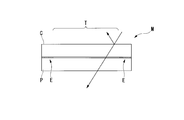
- FIG. 1A is a cross-sectional view showing a touch panel in the present embodiment.
- FIG. 1B is an enlarged view of an edge portion of the touch panel in the present embodiment.
- FIG. 2 is a perspective view showing the touch panel in the present embodiment.
- symbol M is a touchscreen.
- a touch panel substrate P having a display area T and capable of display and touch operation, and a cover substrate C formed of a transparent substrate such as glass are provided. Arranged in layers. Further, between the touch panel substrate P and the cover substrate C, a connection portion is provided at an edge E around the display region T in the region excluding the display region T.
- the touch panel substrate P can be used for mobile terminal devices such as mobile phones.
- the touch panel substrate P may have a structure in which a touch panel sensor unit and a liquid crystal display device are combined. Further, the touch panel substrate P is filled with a transparent adhesive between a display surface of the liquid crystal display element and a back surface of the input area of the touch switch in a display device including a transparent touch switch and a liquid crystal display element. You may have the structure where the liquid crystal display element was adhere
- the cover substrate C is a transparent substrate such as glass or resin laminated glass, and is stacked on the touch panel substrate P so as to cover the outermost surface side of the touch panel M.
- the display area T has an area having a predetermined size and shape in the in-plane direction orthogonal to the viewing direction, and can have, for example, a rectangular area arranged at the in-plane center position of the touch panel substrate P.
- the outer side of the display area T in the substrate surface is an edge (frame part) E.
- the edge E allows a predetermined color to be recognized when the touch panel M is visually recognized, and a color layer D and a shielding layer S as a connection part connected (contacted) to both the cover substrate C and the touch panel substrate P. Are laminated from the cover substrate C side to the touch panel substrate P side.
- a color layer D is laminated on the surface of the cover substrate C on the touch panel substrate P side, and a shielding layer S is laminated on the color layer D.
- the position where the connection portion is installed is not limited to the edge portion E, and the connection portion can be formed in a desired region.
- the color layer D is a non-light-transmitting film (light-blocking film) and is an optical thin film formed from multilayer films having different refractive indexes in order to produce a desired color.
- the color layer D is a multilayer structure in which a large number of high refractive index layers D1 formed of a high refractive index material and low refractive index layers D2 formed of a low refractive index material are alternately stacked. .
- the high refractive index layer D1 can be formed from a high refractive index material such as titanium oxide, and the low refractive index layer D2 can be formed from a low refractive index material such as silicon oxide.
- These high-refractive materials and low-refractive materials need only have different refractive indexes, and the film thickness and the number of layers are, for example, n layers of ⁇ / 4 thin films with respect to the wavelength ⁇ desired to be expressed by the color layer D. Thus, a desired color can be realized.
- the larger the refractive index difference between the high refractive material and the low refractive material the smaller the number of layers can be set.
- the dielectric film material for forming the high refractive index layer D1 and the low refractive index layer D2 can be selected from the materials exemplified below. Furthermore, it is also possible to select and combine two or three of these. Here, the level of the refractive index is set by comparing the selected materials, and depending on the combination of materials, it may be switched between the low refractive index material and the high refractive material.
- Low refractive material SiOx, SiN, SiOxNy, Al 2 O 3, AlN, MgO, MgF 2, HfO 2 ⁇
- High refractive materials Ta 2 O 5 , NbxOy, TiO 2 , Ti 3 O 5 , ZnO, ZrO 2
- color layer C an example of setting the film thickness and the number of layers for four colors of red, yellow, blue, and green is illustrated in Table 1.
- the low refractive index layer D2 has a thickness dimension of about 100 nm
- the high refractive index layer D1 has a thickness dimension of about 2/3 to 1/2 of the low refractive index layer D2.
- D2 can be set thicker than the high refractive index layer D1.
- the shielding layer S is a film having a non-light-transmitting property (light-shielding property) and has a dielectric constant similar to that of a substrate such as glass and does not block radio waves.
- the shielding layer S is a multilayer structure in which a large number of multilayer films having different dielectric constants are alternately stacked in order to have a desired dielectric constant. Specifically, a large number of metal layers S1 formed from a low dielectric constant material and dielectric layers S2 formed from a high dielectric constant material are stacked.
- the metal layer S1 can be formed from a material such as titanium or aluminum, and the dielectric layer S2 can be formed from a high dielectric constant material such as silicon oxide.
- the dielectric material and the metal material are alternately laminated, and the shielding layer S does not transmit visible light and has a desired state having the same dielectric constant as that of the substrate such as glass.
- the thickness and the number of layers are set.
- the dielectric material can be selected from the materials exemplified as the dielectric film material in the color layer D described above. Further, two or three of these can be selected and combined.
- the metal material can be selected from the following materials in consideration of the characteristics of shielding properties and dielectric constant. Two or three of these can be selected and combined.
- Metal materials Si, Ti, Ta, Nb, Al, Ag, Mg, Sb, Zr, Zn, Sn, Ca, Au, Cr, Ge, In, Ni, Pt
- each of the metal layers S1 constituting the shielding layer is formed as a single layer with a thickness on the order of nm so that the shielding layer can shield visible light and at the same time does not block radio waves. Is set to be smaller than the film thickness of the dielectric layer S2. Further, the total film thickness of the stacked metal layers S1 is set to be larger than the minimum necessary film thickness value for not transmitting visible light.
- the shielding performance can be set so that the transmittance is 1% or less in the visible light range.
- the total film thickness of the metal layer S1 is required to be about 50 nm.
- the total film thickness of the laminated dielectric layers S2 is set to be larger than the minimum necessary film thickness value for maintaining a state in which radio waves are not shielded.
- the total thickness of the dielectric layer S2 is required to be about 200 nm. Note that the number of stacked metal layers S1 and dielectric layers S2 can be changed according to the color layer D described above.
- the shielding layer S As an example of the shielding layer S, an example of the film thickness and the number of laminated layers capable of realizing the same dielectric constant 3.5 to 10 ( ⁇ s) as that of glass will be shown.
- the dielectric layer is formed so that the metal layer S1 has a thickness dimension of 0.5 nm to 5 nm, and the dielectric constant layer S2 has a thickness dimension of 1 nm to 10 nm, which is about 2 to 10 times the metal layer S1.
- the layer S2 can be set thicker than the metal layer S1.
- black can be realized by laminating a large number of titanium and silicon oxide like the shielding layer S, or silver can be achieved by laminating a large number of aluminum and silicon oxide.
- connection portion in which the color layer D, which is an optical thin film in this embodiment, and the light shielding layer S are laminated, the total film thickness of the connection portion is 500 nm or less in the case of black and 1 in the case of red. It becomes possible to set to 5 to 2 ⁇ m. Furthermore, it is possible to form such a connection portion by sputtering without using a wet process such as a printing process (printing process).
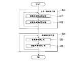
- FIG. 3 is a flowchart showing a method for manufacturing a touch panel in the present embodiment.
- a cover substrate C formed of glass is prepared, and a color layer film forming step S10 is performed on the cover substrate C provided with a mask in the display region T as shown in FIG.
- a color layer D is formed as a cover layer C, and then a shield layer S is formed as a shield layer formation step S20. Thereafter, the mask is removed, and the cover substrate C (the color layer D and the shield layer S are laminated) An optical thin film substrate) and a touch panel substrate are bonded together.
- the high refractive index layer D1 and the low refractive index layer D2 are stacked with a material appropriately selected as the color layer D so that the color layer D has a predetermined thickness.
- the color layer D is formed by sputtering by repeating the high refractive index layer deposition step S11 and the low high refractive index layer deposition step S12 many times.
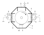
- FIG. 4 shows a carousel type sputtering apparatus as an example of the apparatus in this embodiment.
- FIG. 4 is a schematic diagram showing a manufacturing apparatus used for manufacturing one embodiment of the touch panel in the present embodiment.
- the manufacturing apparatus according to this embodiment is a carousel type sputtering apparatus. As shown in FIG. 4, the manufacturing apparatus according to this embodiment has a drum 2 that rotates with a substrate holder 10 mounted in a chamber 1, and can sputter different materials facing the outer peripheral position of the drum 2.
- an AC cathode 6 that is provided as a position corresponding to the substrate holder 10 of each rotating drum 2 and connected to an AC power source 7, and a gas that supplies a gas such as Ar into the chimney
- An inlet 8 is provided in each of the CA1 chimney 3 and the CA2 chimney 4.
- the substrate holder 10 is attached with a cover substrate C in which a mask is formed on the surface portion corresponding to the display region T, or a cover substrate C in which a color layer D is further formed.
- the cathodes 6 of the CA1 chimney 3 and the CA2 chimney 4 are titanium that is a titanium oxide source as an example of a high refractive index material and a silicon oxide source that is an example of a low refractive index material. Install each with silicon. Thereafter, the cover substrate C on which the mask is formed is fixed to the substrate holder 10 of the drum 2. Further, a gas such as argon is supplied from the gas introduction port 8, and at the same time, an oxidation source such as oxygen gas is supplied to the oxidation source supply unit 5 via the gas introduction port 9 to rotate the drum 2.
- a high refractive index layer D1 and a low refractive index layer D2 are laminated with a material appropriately selected as the color layer D so as to have a predetermined film thickness. To do. At this time, the high refractive index layer film forming step S11 and the low refractive index layer film forming step S12 are repeated many times to form the high refractive index layer D1 formed from the high refractive index material and the low refractive index material. A large number of low refractive index layers D2 are alternately laminated.
- the high refractive index layer film forming step S11 and the low refractive index layer film forming step S12 are performed as many times as necessary. Can be repeated.
- the metal layer S1 and the dielectric layer S2 are laminated with a material appropriately selected as the shielding layer S so as to have a predetermined film thickness.
- the metal layer film forming step S21 and the dielectric layer film forming step S22 are repeated many times, and the sputter film is formed so that the shielding layer S becomes a multilayer structure.
- the cathode 6 of the CA1 chimney 3 and the CA2 chimney 4 is provided with titanium as an example of a metal material and silicon as a silicon oxide source as an example of a dielectric constant material. Then, the cover substrate C on which the color layer D is formed is fixed to the substrate holder 10 of the drum 2, and power is supplied from the AC power source 7 to the cathode 6 in a predetermined atmosphere state in which a gas such as argon is supplied from the gas inlet 8. Supply and rotate the drum 2. It is possible to form a titanium film as a metal which is a metal material by this metal sputtering.
- an oxidation source such as oxygen gas is supplied to the oxidation source supply unit 5 through the gas introduction port 9 to supply electric power from the AC power source 7 to the cathode 6 as an oxidizing atmosphere to rotate the drum 2.
- Silicon oxide can be formed by this reactive sputtering.
- the power supplied to the cathode 6 of the CA1 chimney 3 and the CA2 chimney 4 and the presence / absence of the supply of the oxidation source (oxygen gas) to the oxidation source supply unit 5 are controlled so as to be switched alternately.
- the layer film forming step S21 and the dielectric layer forming step S22 are repeated many times. As a result, a large number of dielectric layers S2 formed of a dielectric constant material and metal layers S1 formed of a metal material are alternately stacked.
- the multilayer film can be stacked in one chamber by switching the target between silicon and titanium in the color layer forming step S10 and the shielding layer forming step S20.
- the oxidation source such as oxygen gas
- the reactive sputtering and the metal sputtering are switched, and the color layer forming step S10 and the shielding layer forming step S20 are performed continuously. Is also possible.
- the color layer D is laminated from the cover substrate C side toward the touch panel substrate T side, and the multilayer structure is formed by alternately laminating dielectric layers and metal layers.
- a shielding layer S, and a connecting portion composed of the shielding layer S are provided.
- the touch panel of the present embodiment has a visible light blocking property at the edge E while achieving a desired color development, can maintain a dielectric constant comparable to that of glass, and allows radio waves to pass through. Is possible.
- the thickness of these connecting portions can be made smaller than 2 ⁇ m, there is no gap between the cover substrate C and the touch panel substrate T, and the diffused reflection is prevented and the touch panel M with improved visibility is realized. It becomes possible to do.
- the drum 2 is rotated at 200 rpm, power is supplied to the silicon side while the drum 2 rotates three times, and then the discharge is stopped. Power is supplied to the titanium side.
- the color layer D was formed by supplying oxygen gas as an oxidation source, and the shielding layer S was formed by switching so as not to supply oxygen gas.
- the film configurations shown in Tables 1 and 2 were used.
- the thickness of titanium which is a metal
- the thickness of silicon oxide was made thinner than that of silicon oxide.
- four colors were developed by changing the film configuration.
- a layer having the same dielectric constant as that of glass can be formed for any color, and the visible light transmittance can be reduced to 1% or less.
- it could be formed thinner than the thickness (about 5 ⁇ m) of the connecting portion formed in the printing process.
- a mobile phone As an application example of one embodiment of the present invention, it can be applied to a mobile phone, a smartphone, a tablet, a touch-sensitive notebook PC, a touch panel incorporated in a vending machine with a touch function, and an optical thin film substrate.
Landscapes
- Engineering & Computer Science (AREA)
- Physics & Mathematics (AREA)
- General Engineering & Computer Science (AREA)
- Theoretical Computer Science (AREA)
- General Physics & Mathematics (AREA)
- Human Computer Interaction (AREA)
- Optics & Photonics (AREA)
- Position Input By Displaying (AREA)
- Laminated Bodies (AREA)
Abstract
Description
本願は、2013年7月11日に日本に出願された特願2013-145755号に基づき優先権を主張し、その内容をここに援用する。
このタッチパネルは、光透過性の導電層等が透明基板に積層されるとともに最表面側にフィルムが積層形成されて、静電容量の変化などによって指等の操作位置を検出するタッチパネル基板を有する。
例えば、フィルム状で光透過性を有する上基板及び下基板を備えるタッチパネル基板が知られている。上基板の上面には、酸化インジウム錫等の光透過性を有する略帯状の上導電層が前後方向に複数配列されて形成される。また、酸化インジウム錫等の上に蒸着等によって銅や銀等の導電金属箔が重ねられた複数の上電極が、上導電層とは直交方向である左右方向に形成される。下基板の上面には、酸化インジウム錫等の光透過性を有する略帯状の複数の下導電層が、上導電層と直交する方向の左右方向に配列形成される。また、一端が下導電層端部に連結される上電極と同様の複数の下電極が、下導電層と平行方向の左右方向に形成されている。
図5は従来のタッチパネルの断面図である。図5において、符号Pはタッチパネル基板、符号Cはカバー基板である。カバー基板Cにおいて、タッチパネル基板P側には、操作をおこなうタッチ領域(表示領域)Tの外周または外側に位置する縁部Eに非透光性の遮光膜thが設けられている。
この遮光膜thは、特許文献1のように、カバー基板Cに印刷等により5μm~20μm程度の厚さに形成することが知られている。
さらに、特許文献1のように金属等の導体を縁部Eに設けた場合、カバー基板Cやパネル部Pと縁部Eとの誘電率が異なるため、電波特性などの特性が劣化する可能性があるため好ましくない。
1.視認性の低下を防止すること。
2.縁部の薄厚化を図ること。
3.縁部が、遮光性能を維持したままガラス等から形成される基板と同程度の誘電率を有すること。
また、上記第一態様において、前記カラー層が、高屈折率層および低屈折率層が交互に積層するように構成された多層構造体から形成されていても良い。
また、上記第一態様において、前記低屈折率層及び前記高屈折率層のうち少なくとも1つが、金属元素を含んでいても良い。
本発明の第二態様に係るタッチパネルの製造方法は、カバー基板を準備し、真空中で、前記カバー基板上の表示領域以外の領域に、カラー層を形成し、真空中で、誘電体層が金属層よりも厚くなるように、前記誘電体層および前記金属層が交互に積層することにより得られる多層構造体を有する遮蔽層を、前記カラー層上に形成し、前記遮蔽層上にタッチパネル基板を貼り合わせる。
本発明の第三態様に係る光学薄膜基板は、基板と、前記基板上に設けられたカラー層と、前記カラー層上に設けられ、金属層と前記金属層よりも厚い誘電体層が交互に積層するように構成された多層構造体から形成される遮蔽層と、を含む。
本発明の第三態様において、前記カラー層が、高屈折率層および低屈折率層が交互に積層するように構成された多層構造体から形成されていても良い。
本発明の第三態様において、前記低屈折率層および前記高屈折率層のうち少なくとも1つが、金属元素を含んでいても良い。
本発明の第三態様において、前記基板が、ガラス基板又は樹脂基板であっても良い。
本発明の第四態様に係る光学薄膜基板の製造方法は、基板を準備し、真空中で、前記基板上にカラー層を形成し、真空中で、誘電体層が金属層よりも厚くなるように、前記誘電体層および前記金属層が交互に積層することにより得られる多層構造体を有する遮蔽層を前記カラー層上に形成する。
本発明の第一態様に係るタッチパネルにおいて、前記接続部が、前記カバー基板側から前記タッチパネル基板側に向かって積層されたカラー層と遮蔽層から構成される。前記遮蔽層が、交互に積層した誘電体層および金属層の多層構造体から形成されることにより、表示領域の周囲に設けられた接続部の厚さを低減して、所望の色を有するフレーム(額縁)を表示領域の外部に設けることが可能となる。これにより、カバー基板とタッチパネル基板との間で、表示領域境界付近に段差ができることを防止して、視認性の低下を防止することが可能となる。
本発明の第二態様に係るタッチパネルの製造方法は、真空中で、誘電体層および金属層が交互に積層された多層構造体としての前記遮蔽層を形成する工程を有し、前記遮蔽層を形成する工程において、前記誘電体層を前記金属層よりも厚く積層することにより、表示領域の周囲に設けられた接続部の厚さを低減して、所望の色を有するフレーム(額縁)を表示領域の外部に設けたタッチパネルを製造することが可能となる。これにより、カバー基板とタッチパネル基板との間で、表示領域境界付近に段差ができることを防止して、視認性低下防止を図るタッチパネルを製造することが可能となる。さらに、金属層から形成される導体を、縁部に設けられる接続部に設けた場合でも、本発明の第二態様に係るタッチパネルの製造方法によれば、接続部が金属層と、金属層より厚い誘電体層とを交互に積層した多層構造体から形成されることにより、縁部が遮光性を有した状態で、基板、ガラスなどとほぼ等しい誘電率を維持することが可能となる。また、遮蔽層における所望の遮光性と誘電率とを実現することが可能となるので、電波特性などに悪影響を及ぼすことがないタッチパネルを製造することができる。
図1Aは、本実施形態におけるタッチパネルを示す断面図である。図1Bは、本実施形態におけるタッチパネルの縁部の拡大図である。図2は、本実施形態におけるタッチパネルを示す斜視図である。図1A及び図2において、符号Mは、タッチパネルである。
表示領域Tの基板面内における外側が縁部(額縁部)Eである。この縁部Eには、タッチパネルMの視認時に所定の色を認識可能にさせるとともに、カバー基板Cとタッチパネル基板Pとの両方に接続(接触)する接続部として、カラー層Dと遮蔽層Sとがカバー基板C側からタッチパネル基板P側に向けて積層されている。
・高屈折材料:Ta2O5,NbxOy,TiO2,Ti3O5,ZnO,ZrO2
例えば、上記の材料のうち、低屈折率材料として酸化シリコン(n=1.46)、高屈折率材料として、酸化チタン(n=2.4)の組み合わせを選択することができる。

また、積層した誘電体層S2の合計膜厚が、電波を遮蔽しない状態を維持する必要最低限の膜厚値よりも大きくなるように設定される。具体的には、誘電体層S2の合計膜厚が200nm程度は必要とされる。
なお、上記のカラー層Dに応じて金属層S1及び誘電体層S2の積層数を変更することができる。

本実施形態におけるタッチパネルの製造方法においては、ガラスから形成されるカバー基板Cを用意して、表示領域Tにマスクを設けたカバー基板Cに、図3に示すように、カラー層成膜工程S10としてカラー層Dを成膜し、その後、遮蔽層成膜工程S20として遮蔽層Sを成膜し、その後、マスクを除去して、カラー層Dと遮蔽層Sとが積層されたカバー基板C(光学薄膜基板)とタッチパネル基板とを貼り合わせる。
図4は、本実施形態におけるタッチパネルの一実施形態の製造に用いる製造装置を示す模式図である。
なお、基板ホルダ10には、表示領域Tに対応する表面部分にマスクを形成したカバー基板C、または、さらにカラー層Dの形成されたカバー基板Cを取り付ける。
このとき、高屈折率層成膜工程S11と低屈折率層成膜工程S12とを、多数回繰り返して、高屈折率材料から形成される高屈折率層D1と低屈折率材料から形成される低屈折率層D2とが交互に多数積層される。
このとき、CA1チムニ3とCA2チムニ4とのカソード6に供給する電力を交互に切り替えるように制御することで、高屈折率層成膜工程S11と低屈折率層成膜工程S12とを必要回数繰り返すことができる。
さらに、酸化源供給部5にガス導入口9を介して酸素ガス等の酸化源を供給して、酸化雰囲気として、AC電源7からカソード6に電力供給してドラム2を回転させる。この反応性スパッタにより酸化シリコンを成膜することが可能である。
また、酸化源供給部5への酸素ガス等の酸化源供給を切り替えることによって、反応性スパッタと、金属スパッタとを切り替え、カラー層形成工程S10と遮蔽層形成工程S20とを連続しておこなうことも可能である。また、カラー層Dの発色として黒色を設定した場合など金属スパッタが必要な場合にも切り替え可能である。
以下、本発明の一実施形態に係る実施例を説明する。
具体的には、表1、表2に示す膜構成とした。
さらに、印刷工程にて形成された接続部の厚さ(およそ5μm程度)よりも薄く形成することができた。
Claims (9)
- カバー基板と、
前記カバー基板上の表示領域以外の領域に設けられ、カラー層と、金属層と前記金属層よりも厚い誘電体層とが交互に積層するように構成された多層構造体から形成される遮蔽層と、を含む接続部と、
前記接続部を介在するように前記カバー基板に対向配置されたタッチパネル基板と、
を含むタッチパネル。 - 前記カラー層が、高屈折率層および低屈折率層が交互に積層するように構成された多層構造体から形成される請求項1に記載のタッチパネル。
- 前記低屈折率層及び前記高屈折率層のうち少なくとも1つが、金属元素を含む請求項2に記載のタッチパネル。
- カバー基板を準備し、
真空中で、前記カバー基板上の表示領域以外の領域に、カラー層を形成し、
真空中で、誘電体層が金属層よりも厚くなるように、前記誘電体層および前記金属層が交互に積層することにより得られる多層構造体を有する遮蔽層を、前記カラー層上に形成し、
前記遮蔽層上にタッチパネル基板を貼り合わせる
タッチパネルの製造方法。 - 基板と、
前記基板上に設けられたカラー層と、
前記カラー層上に設けられ、金属層と前記金属層よりも厚い誘電体層が交互に積層するように構成された多層構造体から形成される遮蔽層と、を含む
光学薄膜基板。 - 前記カラー層が、高屈折率層および低屈折率層が交互に積層するように構成された多層構造体から形成される請求項5に記載の光学薄膜基板。
- 前記低屈折率層および前記高屈折率層のうち少なくとも1つが、金属元素を含む請求項6に記載の光学薄膜基板。
- 前記基板が、ガラス基板又は樹脂基板である請求項5に記載の光学薄膜基板。
- 基板を準備し、
真空中で、前記基板上にカラー層を形成し、
真空中で、誘電体層が金属層よりも厚くなるように、前記誘電体層および前記金属層が交互に積層することにより得られる多層構造体を有する遮蔽層を前記カラー層上に形成する
光学薄膜基板の製造方法。
Priority Applications (4)
| Application Number | Priority Date | Filing Date | Title |
|---|---|---|---|
| US14/647,034 US9891731B2 (en) | 2013-07-11 | 2014-07-10 | Touch panel, method of producing the same, optical thin film substrate and method of producing the same |
| KR1020157014085A KR101670040B1 (ko) | 2013-07-11 | 2014-07-10 | 터치 패널, 그 제조 방법, 광학 박막 기판, 및 그 제조 방법 |
| JP2015504805A JP5848851B2 (ja) | 2013-07-11 | 2014-07-10 | タッチパネル、その製造方法、光学薄膜基板、およびその製造方法 |
| CN201480003204.9A CN104838344B (zh) | 2013-07-11 | 2014-07-10 | 触摸面板、触摸面板的制造方法、光学薄膜基板及其制造方法 |
Applications Claiming Priority (2)
| Application Number | Priority Date | Filing Date | Title |
|---|---|---|---|
| JP2013145755 | 2013-07-11 | ||
| JP2013-145755 | 2013-07-11 |
Publications (1)
| Publication Number | Publication Date |
|---|---|
| WO2015005437A1 true WO2015005437A1 (ja) | 2015-01-15 |
Family
ID=52280114
Family Applications (1)
| Application Number | Title | Priority Date | Filing Date |
|---|---|---|---|
| PCT/JP2014/068458 Ceased WO2015005437A1 (ja) | 2013-07-11 | 2014-07-10 | タッチパネル、その製造方法、光学薄膜基板、およびその製造方法 |
Country Status (6)
| Country | Link |
|---|---|
| US (1) | US9891731B2 (ja) |
| JP (1) | JP5848851B2 (ja) |
| KR (1) | KR101670040B1 (ja) |
| CN (1) | CN104838344B (ja) |
| TW (1) | TWI601042B (ja) |
| WO (1) | WO2015005437A1 (ja) |
Cited By (4)
| Publication number | Priority date | Publication date | Assignee | Title |
|---|---|---|---|---|
| KR20160138226A (ko) | 2014-05-01 | 2016-12-02 | 가부시키가이샤 아루박 | 터치 패널, 터치 패널의 제조 방법 및 광학 박막 |
| WO2016201926A1 (en) * | 2015-06-19 | 2016-12-22 | Boe Technology Group Co., Ltd. | Substrate, touch display panel having the same, and manufacturing method thereof |
| JP2017002338A (ja) * | 2015-06-05 | 2017-01-05 | 旭硝子株式会社 | 光学部材および光学部材の製造方法 |
| US9891731B2 (en) | 2013-07-11 | 2018-02-13 | Ulvac, Inc. | Touch panel, method of producing the same, optical thin film substrate and method of producing the same |
Families Citing this family (7)
| Publication number | Priority date | Publication date | Assignee | Title |
|---|---|---|---|---|
| KR20160028595A (ko) * | 2014-09-03 | 2016-03-14 | 삼성디스플레이 주식회사 | 커버 윈도우, 이의 제조 방법 및 이를 포함하는 표시 장치 |
| WO2018180127A1 (ja) * | 2017-03-30 | 2018-10-04 | 富士フイルム株式会社 | 光学部材 |
| CN107741795B (zh) * | 2017-09-30 | 2024-07-09 | 北京集创北方科技股份有限公司 | 触摸屏及其控制方法和终端 |
| EP4583313A3 (en) | 2018-04-06 | 2025-07-16 | 3M Innovative Properties Company | Gradient permittivity film |
| EP3776722B1 (en) | 2018-04-06 | 2023-09-27 | 3M Innovative Properties Company | Gradient permittivity film |
| CN113817986A (zh) * | 2020-06-19 | 2021-12-21 | 比亚迪股份有限公司 | 一种镀膜材料及其制备方法 |
| CN115159861B (zh) * | 2022-07-05 | 2023-10-31 | 上海玻光科技合伙企业(有限合伙) | 一种中性色光学薄膜 |
Citations (3)
| Publication number | Priority date | Publication date | Assignee | Title |
|---|---|---|---|---|
| JP2000105537A (ja) * | 1998-09-30 | 2000-04-11 | Sumitomo Chem Co Ltd | ディスプレイ用前面板 |
| JP2012226688A (ja) * | 2011-04-22 | 2012-11-15 | Toppan Printing Co Ltd | 加飾カバーガラス一体型タッチパネルセンサー |
| JP2013131099A (ja) * | 2011-12-22 | 2013-07-04 | Sanyo Electric Co Ltd | 静電容量型タッチパネル |
Family Cites Families (19)
| Publication number | Priority date | Publication date | Assignee | Title |
|---|---|---|---|---|
| JP2001201745A (ja) | 2000-01-18 | 2001-07-27 | Seiko Epson Corp | 液晶装置及びこれを用いた電子機器 |
| US7502155B2 (en) * | 2005-03-15 | 2009-03-10 | Texas Instruments Incorporated | Antireflective coating for semiconductor devices and method for the same |
| JP2008145664A (ja) | 2006-12-08 | 2008-06-26 | Seiko Epson Corp | 液晶装置及び電子機器 |
| US20080165139A1 (en) * | 2007-01-05 | 2008-07-10 | Apple Inc. | Touch screen stack-up processing |
| JP5003354B2 (ja) | 2007-08-28 | 2012-08-15 | 三菱化学株式会社 | 積層体及びそれを用いる光学特性制御方法 |
| KR20100040114A (ko) | 2008-10-09 | 2010-04-19 | 주식회사 유아이디 | 플라즈마 디스플레이 패널 필터 |
| JP5712571B2 (ja) | 2009-11-20 | 2015-05-07 | 東レ株式会社 | ハーフミラー調タッチセンサー |
| KR101773514B1 (ko) * | 2010-12-15 | 2017-09-01 | 삼성디스플레이 주식회사 | 터치스크린 일체형 평판표시장치 |
| CN102810020A (zh) | 2011-06-02 | 2012-12-05 | 东莞万士达液晶显示器有限公司 | 触控面板 |
| KR20120134955A (ko) * | 2011-06-03 | 2012-12-12 | (주)네패스디스플레이 | 시인성이 향상된 터치 패널 및 그 제조방법 |
| CN103049119A (zh) | 2011-10-14 | 2013-04-17 | 联胜(中国)科技有公司 | 触控装置及触控显示装置 |
| US9259904B2 (en) * | 2011-10-20 | 2016-02-16 | Apple Inc. | Opaque thin film passivation |
| CN105867690B (zh) | 2011-11-02 | 2019-02-12 | 群康科技(深圳)有限公司 | 影像显示系统及触控感测装置的制造方法 |
| EP2793061A4 (en) * | 2011-12-12 | 2015-09-16 | Konica Minolta Inc | OPTICAL LAMINATED FOIL, INFRARED PROTECTION FILM AND INFRARED VISOR BODY |
| KR101524449B1 (ko) * | 2011-12-22 | 2015-06-02 | 엘지디스플레이 주식회사 | 액정표시장치 및 그 제조방법 |
| JP6016051B2 (ja) | 2012-01-25 | 2016-10-26 | 大日本印刷株式会社 | 表示装置用前面保護板、及び表示装置 |
| JP2013245151A (ja) | 2012-05-28 | 2013-12-09 | Asahi Glass Co Ltd | 筐体用結晶化ガラスおよび結晶化ガラスの製造方法 |
| CN203025672U (zh) | 2012-12-20 | 2013-06-26 | 瑞世达科技(厦门)有限公司 | 触控面板及其盖板结构 |
| WO2015005437A1 (ja) | 2013-07-11 | 2015-01-15 | 株式会社アルバック | タッチパネル、その製造方法、光学薄膜基板、およびその製造方法 |
-
2014
- 2014-07-10 WO PCT/JP2014/068458 patent/WO2015005437A1/ja not_active Ceased
- 2014-07-10 CN CN201480003204.9A patent/CN104838344B/zh active Active
- 2014-07-10 US US14/647,034 patent/US9891731B2/en active Active
- 2014-07-10 KR KR1020157014085A patent/KR101670040B1/ko active Active
- 2014-07-10 JP JP2015504805A patent/JP5848851B2/ja active Active
- 2014-07-11 TW TW103124017A patent/TWI601042B/zh active
Patent Citations (3)
| Publication number | Priority date | Publication date | Assignee | Title |
|---|---|---|---|---|
| JP2000105537A (ja) * | 1998-09-30 | 2000-04-11 | Sumitomo Chem Co Ltd | ディスプレイ用前面板 |
| JP2012226688A (ja) * | 2011-04-22 | 2012-11-15 | Toppan Printing Co Ltd | 加飾カバーガラス一体型タッチパネルセンサー |
| JP2013131099A (ja) * | 2011-12-22 | 2013-07-04 | Sanyo Electric Co Ltd | 静電容量型タッチパネル |
Cited By (6)
| Publication number | Priority date | Publication date | Assignee | Title |
|---|---|---|---|---|
| US9891731B2 (en) | 2013-07-11 | 2018-02-13 | Ulvac, Inc. | Touch panel, method of producing the same, optical thin film substrate and method of producing the same |
| KR20160138226A (ko) | 2014-05-01 | 2016-12-02 | 가부시키가이샤 아루박 | 터치 패널, 터치 패널의 제조 방법 및 광학 박막 |
| US10429964B2 (en) | 2014-05-01 | 2019-10-01 | Ulvac, Inc. | Touch panel, method of manufacturing touch panel, and optical thin film |
| JP2017002338A (ja) * | 2015-06-05 | 2017-01-05 | 旭硝子株式会社 | 光学部材および光学部材の製造方法 |
| WO2016201926A1 (en) * | 2015-06-19 | 2016-12-22 | Boe Technology Group Co., Ltd. | Substrate, touch display panel having the same, and manufacturing method thereof |
| US10133379B2 (en) | 2015-06-19 | 2018-11-20 | Boe Technology Group Co., Ltd. | Substrate, touch display panel having the same, and method thereof |
Also Published As
| Publication number | Publication date |
|---|---|
| KR101670040B1 (ko) | 2016-10-27 |
| TWI601042B (zh) | 2017-10-01 |
| CN104838344A (zh) | 2015-08-12 |
| JPWO2015005437A1 (ja) | 2017-03-02 |
| TW201512938A (zh) | 2015-04-01 |
| CN104838344B (zh) | 2018-01-12 |
| KR20150079891A (ko) | 2015-07-08 |
| US9891731B2 (en) | 2018-02-13 |
| US20160109971A1 (en) | 2016-04-21 |
| JP5848851B2 (ja) | 2016-01-27 |
Similar Documents
| Publication | Publication Date | Title |
|---|---|---|
| JP5848851B2 (ja) | タッチパネル、その製造方法、光学薄膜基板、およびその製造方法 | |
| CN115811899B (zh) | 一种显示面板及显示装置 | |
| CN105204692B (zh) | 一种触摸屏、显示装置及显示装置的显示驱动方法 | |
| JP5375536B2 (ja) | 静電容量式タッチパネルとその製造方法及び該タッチパネルを備えた液晶表示装置 | |
| US8643629B2 (en) | Color filter with touch screen function and liquid crystal display device | |
| KR20120025977A (ko) | 전극 필름 및 좌표 검출 장치 | |
| WO2014187090A1 (zh) | 彩色滤光阵列基板及其制造方法、显示装置 | |
| KR20150014208A (ko) | 터치센서 | |
| JP2006268085A (ja) | タッチパネル | |
| CN105579939A (zh) | 用于输入装置的电极及其制造方法 | |
| WO2016158181A1 (ja) | 窒素含有Cu合金膜、積層膜、およびこれらの製造方法、ならびにCu合金スパッタリングターゲット | |
| JP2004361662A (ja) | 導電性透明積層体 | |
| JP6122216B2 (ja) | タッチパネル及びその製造方法、並びに、表示装置及びその製造方法 | |
| KR102330898B1 (ko) | 터치 패널 및 터치 패널 제조 방법 | |
| CN108290381A (zh) | 叠层体基板、导电性基板、叠层体基板的制造方法、导电性基板的制造方法 | |
| TW201719348A (zh) | 金屬網格觸控模組及其適用之觸控顯示裝置 | |
| JP6157424B2 (ja) | 電極およびその製造方法 | |
| KR20090003993A (ko) | 반사기능을 갖는 터치 패널용 반투명의 이중 기능성 필름제조방법 및 이에 의해 제조된 반사기능을 갖는 터치패널용 반투명의 이중 기능성 필름 | |
| JP2006120916A (ja) | 透明導電性積層体およびそれを用いたディスプレイ用フィルタ | |
| JP2013175240A (ja) | 静電容量式タッチパネル及び該タッチパネルを備えた液晶表示装置 | |
| WO2026094695A1 (ja) | タッチパネル機能を有する発光装置及びそれを用いた表示装置 | |
| WO2016088688A1 (ja) | 電極およびその製造方法 |
Legal Events
| Date | Code | Title | Description |
|---|---|---|---|
| ENP | Entry into the national phase |
Ref document number: 2015504805 Country of ref document: JP Kind code of ref document: A |
|
| 121 | Ep: the epo has been informed by wipo that ep was designated in this application |
Ref document number: 14822278 Country of ref document: EP Kind code of ref document: A1 |
|
| WWE | Wipo information: entry into national phase |
Ref document number: 14647034 Country of ref document: US |
|
| ENP | Entry into the national phase |
Ref document number: 20157014085 Country of ref document: KR Kind code of ref document: A |
|
| NENP | Non-entry into the national phase |
Ref country code: DE |
|
| 122 | Ep: pct application non-entry in european phase |
Ref document number: 14822278 Country of ref document: EP Kind code of ref document: A1 |