WO2015002213A1 - 発光材料、遅延蛍光体、有機発光素子および化合物 - Google Patents
発光材料、遅延蛍光体、有機発光素子および化合物 Download PDFInfo
- Publication number
- WO2015002213A1 WO2015002213A1 PCT/JP2014/067611 JP2014067611W WO2015002213A1 WO 2015002213 A1 WO2015002213 A1 WO 2015002213A1 JP 2014067611 W JP2014067611 W JP 2014067611W WO 2015002213 A1 WO2015002213 A1 WO 2015002213A1
- Authority
- WO
- WIPO (PCT)
- Prior art keywords
- compound
- general formula
- group
- light emitting
- represented
- Prior art date
Links
- 0 CC1C(C2(C)C)C2=C*1 Chemical compound CC1C(C2(C)C)C2=C*1 0.000 description 8
- AOIMASANFSNKOU-UHFFFAOYSA-N CC(C)c(cc(cc1c2c3c(C(C)C)cc(-c4ccccc4)c2)-c2ccccc2)c1[n]3-c(cc1Oc2c3cccc2)ccc1C3=O Chemical compound CC(C)c(cc(cc1c2c3c(C(C)C)cc(-c4ccccc4)c2)-c2ccccc2)c1[n]3-c(cc1Oc2c3cccc2)ccc1C3=O AOIMASANFSNKOU-UHFFFAOYSA-N 0.000 description 1
- LHVDSZAZTNGBTN-UHFFFAOYSA-N CC(C)c(cc1)cc2c1Oc1ccccc1C21c2ccccc2N(c(cc2)ccc2-c(cc2Oc3c4cccc3)ccc2C4=O)c2c1cccc2 Chemical compound CC(C)c(cc1)cc2c1Oc1ccccc1C21c2ccccc2N(c(cc2)ccc2-c(cc2Oc3c4cccc3)ccc2C4=O)c2c1cccc2 LHVDSZAZTNGBTN-UHFFFAOYSA-N 0.000 description 1
- FOTOOSBWBQQPBE-UHFFFAOYSA-N CC(C)c(cc1)cc2c1Oc1ccccc1C21c2ccccc2N(c(cc2Oc3c4cccc3)ccc2C4=O)c2c1cccc2 Chemical compound CC(C)c(cc1)cc2c1Oc1ccccc1C21c2ccccc2N(c(cc2Oc3c4cccc3)ccc2C4=O)c2c1cccc2 FOTOOSBWBQQPBE-UHFFFAOYSA-N 0.000 description 1
- YPHNDZSQYWPTHJ-UHFFFAOYSA-N CC(C)c(cc1)cc2c1Sc1ccccc1C21c2ccccc2N(c(cc2)ccc2-c(cc2Oc3ccccc33)ccc2C3=O)c2c1cccc2 Chemical compound CC(C)c(cc1)cc2c1Sc1ccccc1C21c2ccccc2N(c(cc2)ccc2-c(cc2Oc3ccccc33)ccc2C3=O)c2c1cccc2 YPHNDZSQYWPTHJ-UHFFFAOYSA-N 0.000 description 1
- XBTWOKAPAZYQRN-UHFFFAOYSA-N CC(C)c1cc(-c2ccccc2)cc(c2c3)c1[nH]c2c(C(C)C)cc3-c1ccccc1 Chemical compound CC(C)c1cc(-c2ccccc2)cc(c2c3)c1[nH]c2c(C(C)C)cc3-c1ccccc1 XBTWOKAPAZYQRN-UHFFFAOYSA-N 0.000 description 1
- NIJYUTRGVZAABN-RNTQUGAFSA-N CC/C=C\C(\[n]1c(-c2cc(-c3nc(cccc4)c4[n]3-c3ccccc3)cc(-c3nc(CCC=C4)c4[n]3-c3ccccc3)c2)nc2c1cccc2)=C/C Chemical compound CC/C=C\C(\[n]1c(-c2cc(-c3nc(cccc4)c4[n]3-c3ccccc3)cc(-c3nc(CCC=C4)c4[n]3-c3ccccc3)c2)nc2c1cccc2)=C/C NIJYUTRGVZAABN-RNTQUGAFSA-N 0.000 description 1
- UVVXLOCWNVGCTL-UHFFFAOYSA-N CC1[I](c(cc2Oc3cc(N(c4c5cccc4)c4ccccc4C54c(cccc5)c5Sc5c4cccc5)ccc33)ccc2C3=O)c(cccc2)c2-c(cccc2)c2Sc2ccccc2-c2c1cccc2 Chemical compound CC1[I](c(cc2Oc3cc(N(c4c5cccc4)c4ccccc4C54c(cccc5)c5Sc5c4cccc5)ccc33)ccc2C3=O)c(cccc2)c2-c(cccc2)c2Sc2ccccc2-c2c1cccc2 UVVXLOCWNVGCTL-UHFFFAOYSA-N 0.000 description 1
- PAIRPRDVPITKEE-UHFFFAOYSA-N CCC1(CC)c2ccccc2N(c(cc2)cc(Oc3cc(N(c4c(C5(CC)CC)cccc4)c4c5cccc4)ccc33)c2C3=O)c2c1cccc2 Chemical compound CCC1(CC)c2ccccc2N(c(cc2)cc(Oc3cc(N(c4c(C5(CC)CC)cccc4)c4c5cccc4)ccc33)c2C3=O)c2c1cccc2 PAIRPRDVPITKEE-UHFFFAOYSA-N 0.000 description 1
- GMAQSYPTHBNSQR-UHFFFAOYSA-N CCC1(CC)c2ccccc2N(c(cc2)ccc2-c(cc2Oc3c4cccc3)ccc2C4=O)c2c1cccc2 Chemical compound CCC1(CC)c2ccccc2N(c(cc2)ccc2-c(cc2Oc3c4cccc3)ccc2C4=O)c2c1cccc2 GMAQSYPTHBNSQR-UHFFFAOYSA-N 0.000 description 1
- FCEOLZQBVCBMQY-UHFFFAOYSA-N CCC1(CC)c2ccccc2N(c(cc2Oc3c4cccc3)ccc2C4=O)c2c1cccc2 Chemical compound CCC1(CC)c2ccccc2N(c(cc2Oc3c4cccc3)ccc2C4=O)c2c1cccc2 FCEOLZQBVCBMQY-UHFFFAOYSA-N 0.000 description 1
- YVYUDHCQHHNSKN-UHFFFAOYSA-N C[BrH]c(cc1Oc2c3cccc2)ccc1C3=O Chemical compound C[BrH]c(cc1Oc2c3cccc2)ccc1C3=O YVYUDHCQHHNSKN-UHFFFAOYSA-N 0.000 description 1
- YIGADUBPJBCYLI-UHFFFAOYSA-N O=C(c(c(Oc1c2)c3)ccc3N(c3c4cccc3)c3ccccc3C43c4ccccc4Oc4c3cccc4)c1ccc2N(c1c(C23c(cccc4)c4Oc4c2cccc4)cccc1)c1c3cccc1 Chemical compound O=C(c(c(Oc1c2)c3)ccc3N(c3c4cccc3)c3ccccc3C43c4ccccc4Oc4c3cccc4)c1ccc2N(c1c(C23c(cccc4)c4Oc4c2cccc4)cccc1)c1c3cccc1 YIGADUBPJBCYLI-UHFFFAOYSA-N 0.000 description 1
- BRSUMTYLGNBFLO-UHFFFAOYSA-N O=C(c(ccc(N1c2ccccc2C2(c3ccccc3-c3ccccc23)c2c1cccc2)c1)c1Oc1c2)c1ccc2N1c2ccccc2C2(c3ccccc3-c3ccccc23)c2c1cccc2 Chemical compound O=C(c(ccc(N1c2ccccc2C2(c3ccccc3-c3ccccc23)c2c1cccc2)c1)c1Oc1c2)c1ccc2N1c2ccccc2C2(c3ccccc3-c3ccccc23)c2c1cccc2 BRSUMTYLGNBFLO-UHFFFAOYSA-N 0.000 description 1
- NKYUORWAVDRFHD-UHFFFAOYSA-N O=C(c(cccc1)c1Oc1c2)c1ccc2-c(cc1)ccc1N(c1c2cccc1)c1ccccc1C21c2ccccc2Sc2ccccc12 Chemical compound O=C(c(cccc1)c1Oc1c2)c1ccc2-c(cc1)ccc1N(c1c2cccc1)c1ccccc1C21c2ccccc2Sc2ccccc12 NKYUORWAVDRFHD-UHFFFAOYSA-N 0.000 description 1
- PSZZCKNNZUONFS-UHFFFAOYSA-N O=C(c(cccc1)c1Oc1c2)c1ccc2-c(cc1)ccc1N1c2ccccc2C(c2ccccc2)(c2ccccc2)c2c1cccc2 Chemical compound O=C(c(cccc1)c1Oc1c2)c1ccc2-c(cc1)ccc1N1c2ccccc2C(c2ccccc2)(c2ccccc2)c2c1cccc2 PSZZCKNNZUONFS-UHFFFAOYSA-N 0.000 description 1
- RMWZHQAVDCEDLG-UHFFFAOYSA-N O=C(c(cccc1)c1Oc1c2)c1ccc2N(c1c(C2(c3ccccc3)c3ccccc3)cccc1)c1c2cccc1 Chemical compound O=C(c(cccc1)c1Oc1c2)c1ccc2N(c1c(C2(c3ccccc3)c3ccccc3)cccc1)c1c2cccc1 RMWZHQAVDCEDLG-UHFFFAOYSA-N 0.000 description 1
- IBCWDIZDAWRNRR-UHFFFAOYSA-N O=C(c(cccc1)c1Oc1c2)c1ccc2N(c1c2cccc1)c1ccccc1C21c2ccccc2Sc2ccccc12 Chemical compound O=C(c(cccc1)c1Oc1c2)c1ccc2N(c1c2cccc1)c1ccccc1C21c2ccccc2Sc2ccccc12 IBCWDIZDAWRNRR-UHFFFAOYSA-N 0.000 description 1
- SJWSTGFQASSRPF-UHFFFAOYSA-N O=C(c(cccc1)c1Oc1c2)c1ccc2N1c2ccccc2C2(c3ccccc3-c3ccccc23)c2c1cccc2 Chemical compound O=C(c(cccc1)c1Oc1c2)c1ccc2N1c2ccccc2C2(c3ccccc3-c3ccccc23)c2c1cccc2 SJWSTGFQASSRPF-UHFFFAOYSA-N 0.000 description 1
- NRIQXTXCSWCUTI-UHFFFAOYSA-N O=C1c(ccc(-c(cc2)ccc2N(c2c3cccc2)c2ccccc2C32c3ccccc3Oc3c2cccc3)c2)c2Oc2c1cccc2 Chemical compound O=C1c(ccc(-c(cc2)ccc2N(c2c3cccc2)c2ccccc2C32c3ccccc3Oc3c2cccc3)c2)c2Oc2c1cccc2 NRIQXTXCSWCUTI-UHFFFAOYSA-N 0.000 description 1
- KBYLUGIKPPBXAR-UHFFFAOYSA-N O=C1c(ccc(-c(cc2)ccc2N2c3ccccc3C3(c4ccccc4-c4ccccc34)c3c2cccc3)c2)c2Oc2ccccc12 Chemical compound O=C1c(ccc(-c(cc2)ccc2N2c3ccccc3C3(c4ccccc4-c4ccccc34)c3c2cccc3)c2)c2Oc2ccccc12 KBYLUGIKPPBXAR-UHFFFAOYSA-N 0.000 description 1
- ACWGOAGJZIOEJZ-UHFFFAOYSA-N O=C1c(ccc(N(c2c(C34c5ccccc5Oc5ccccc35)cccc2)c2c4cccc2)c2)c2Oc2c1cccc2 Chemical compound O=C1c(ccc(N(c2c(C34c5ccccc5Oc5ccccc35)cccc2)c2c4cccc2)c2)c2Oc2c1cccc2 ACWGOAGJZIOEJZ-UHFFFAOYSA-N 0.000 description 1
- RXDPAJXAUFZKFX-UHFFFAOYSA-N O=C1c(ccc(N2c3ccccc3C(c3ccccc3)(c3ccccc3)c3c2cccc3)c2)c2Oc2cc(N3c4ccccc4C(c4ccccc4)(c4ccccc4)c4c3cccc4)ccc12 Chemical compound O=C1c(ccc(N2c3ccccc3C(c3ccccc3)(c3ccccc3)c3c2cccc3)c2)c2Oc2cc(N3c4ccccc4C(c4ccccc4)(c4ccccc4)c4c3cccc4)ccc12 RXDPAJXAUFZKFX-UHFFFAOYSA-N 0.000 description 1
Images


Classifications
-
- C—CHEMISTRY; METALLURGY
- C07—ORGANIC CHEMISTRY
- C07D—HETEROCYCLIC COMPOUNDS
- C07D405/00—Heterocyclic compounds containing both one or more hetero rings having oxygen atoms as the only ring hetero atoms, and one or more rings having nitrogen as the only ring hetero atom
- C07D405/14—Heterocyclic compounds containing both one or more hetero rings having oxygen atoms as the only ring hetero atoms, and one or more rings having nitrogen as the only ring hetero atom containing three or more hetero rings
-
- C—CHEMISTRY; METALLURGY
- C07—ORGANIC CHEMISTRY
- C07D—HETEROCYCLIC COMPOUNDS
- C07D405/00—Heterocyclic compounds containing both one or more hetero rings having oxygen atoms as the only ring hetero atoms, and one or more rings having nitrogen as the only ring hetero atom
- C07D405/02—Heterocyclic compounds containing both one or more hetero rings having oxygen atoms as the only ring hetero atoms, and one or more rings having nitrogen as the only ring hetero atom containing two hetero rings
- C07D405/04—Heterocyclic compounds containing both one or more hetero rings having oxygen atoms as the only ring hetero atoms, and one or more rings having nitrogen as the only ring hetero atom containing two hetero rings directly linked by a ring-member-to-ring-member bond
-
- C—CHEMISTRY; METALLURGY
- C07—ORGANIC CHEMISTRY
- C07D—HETEROCYCLIC COMPOUNDS
- C07D405/00—Heterocyclic compounds containing both one or more hetero rings having oxygen atoms as the only ring hetero atoms, and one or more rings having nitrogen as the only ring hetero atom
- C07D405/02—Heterocyclic compounds containing both one or more hetero rings having oxygen atoms as the only ring hetero atoms, and one or more rings having nitrogen as the only ring hetero atom containing two hetero rings
- C07D405/10—Heterocyclic compounds containing both one or more hetero rings having oxygen atoms as the only ring hetero atoms, and one or more rings having nitrogen as the only ring hetero atom containing two hetero rings linked by a carbon chain containing aromatic rings
-
- C—CHEMISTRY; METALLURGY
- C07—ORGANIC CHEMISTRY
- C07D—HETEROCYCLIC COMPOUNDS
- C07D409/00—Heterocyclic compounds containing two or more hetero rings, at least one ring having sulfur atoms as the only ring hetero atoms
- C07D409/02—Heterocyclic compounds containing two or more hetero rings, at least one ring having sulfur atoms as the only ring hetero atoms containing two hetero rings
- C07D409/04—Heterocyclic compounds containing two or more hetero rings, at least one ring having sulfur atoms as the only ring hetero atoms containing two hetero rings directly linked by a ring-member-to-ring-member bond
-
- C—CHEMISTRY; METALLURGY
- C07—ORGANIC CHEMISTRY
- C07D—HETEROCYCLIC COMPOUNDS
- C07D409/00—Heterocyclic compounds containing two or more hetero rings, at least one ring having sulfur atoms as the only ring hetero atoms
- C07D409/02—Heterocyclic compounds containing two or more hetero rings, at least one ring having sulfur atoms as the only ring hetero atoms containing two hetero rings
- C07D409/10—Heterocyclic compounds containing two or more hetero rings, at least one ring having sulfur atoms as the only ring hetero atoms containing two hetero rings linked by a carbon chain containing aromatic rings
-
- C—CHEMISTRY; METALLURGY
- C07—ORGANIC CHEMISTRY
- C07D—HETEROCYCLIC COMPOUNDS
- C07D413/00—Heterocyclic compounds containing two or more hetero rings, at least one ring having nitrogen and oxygen atoms as the only ring hetero atoms
- C07D413/14—Heterocyclic compounds containing two or more hetero rings, at least one ring having nitrogen and oxygen atoms as the only ring hetero atoms containing three or more hetero rings
-
- C—CHEMISTRY; METALLURGY
- C07—ORGANIC CHEMISTRY
- C07D—HETEROCYCLIC COMPOUNDS
- C07D491/00—Heterocyclic compounds containing in the condensed ring system both one or more rings having oxygen atoms as the only ring hetero atoms and one or more rings having nitrogen atoms as the only ring hetero atoms, not provided for by groups C07D451/00 - C07D459/00, C07D463/00, C07D477/00 or C07D489/00
- C07D491/02—Heterocyclic compounds containing in the condensed ring system both one or more rings having oxygen atoms as the only ring hetero atoms and one or more rings having nitrogen atoms as the only ring hetero atoms, not provided for by groups C07D451/00 - C07D459/00, C07D463/00, C07D477/00 or C07D489/00 in which the condensed system contains two hetero rings
- C07D491/10—Spiro-condensed systems
- C07D491/107—Spiro-condensed systems with only one oxygen atom as ring hetero atom in the oxygen-containing ring
-
- C—CHEMISTRY; METALLURGY
- C07—ORGANIC CHEMISTRY
- C07D—HETEROCYCLIC COMPOUNDS
- C07D495/00—Heterocyclic compounds containing in the condensed system at least one hetero ring having sulfur atoms as the only ring hetero atoms
- C07D495/02—Heterocyclic compounds containing in the condensed system at least one hetero ring having sulfur atoms as the only ring hetero atoms in which the condensed system contains two hetero rings
- C07D495/10—Spiro-condensed systems
-
- C—CHEMISTRY; METALLURGY
- C07—ORGANIC CHEMISTRY
- C07D—HETEROCYCLIC COMPOUNDS
- C07D519/00—Heterocyclic compounds containing more than one system of two or more relevant hetero rings condensed among themselves or condensed with a common carbocyclic ring system not provided for in groups C07D453/00 or C07D455/00
-
- C—CHEMISTRY; METALLURGY
- C09—DYES; PAINTS; POLISHES; NATURAL RESINS; ADHESIVES; COMPOSITIONS NOT OTHERWISE PROVIDED FOR; APPLICATIONS OF MATERIALS NOT OTHERWISE PROVIDED FOR
- C09B—ORGANIC DYES OR CLOSELY-RELATED COMPOUNDS FOR PRODUCING DYES, e.g. PIGMENTS; MORDANTS; LAKES
- C09B11/00—Diaryl- or thriarylmethane dyes
- C09B11/28—Pyronines ; Xanthon, thioxanthon, selenoxanthan, telluroxanthon dyes
-
- C—CHEMISTRY; METALLURGY
- C09—DYES; PAINTS; POLISHES; NATURAL RESINS; ADHESIVES; COMPOSITIONS NOT OTHERWISE PROVIDED FOR; APPLICATIONS OF MATERIALS NOT OTHERWISE PROVIDED FOR
- C09B—ORGANIC DYES OR CLOSELY-RELATED COMPOUNDS FOR PRODUCING DYES, e.g. PIGMENTS; MORDANTS; LAKES
- C09B15/00—Acridine dyes
-
- C—CHEMISTRY; METALLURGY
- C09—DYES; PAINTS; POLISHES; NATURAL RESINS; ADHESIVES; COMPOSITIONS NOT OTHERWISE PROVIDED FOR; APPLICATIONS OF MATERIALS NOT OTHERWISE PROVIDED FOR
- C09B—ORGANIC DYES OR CLOSELY-RELATED COMPOUNDS FOR PRODUCING DYES, e.g. PIGMENTS; MORDANTS; LAKES
- C09B17/00—Azine dyes
- C09B17/02—Azine dyes of the benzene series
-
- C—CHEMISTRY; METALLURGY
- C09—DYES; PAINTS; POLISHES; NATURAL RESINS; ADHESIVES; COMPOSITIONS NOT OTHERWISE PROVIDED FOR; APPLICATIONS OF MATERIALS NOT OTHERWISE PROVIDED FOR
- C09B—ORGANIC DYES OR CLOSELY-RELATED COMPOUNDS FOR PRODUCING DYES, e.g. PIGMENTS; MORDANTS; LAKES
- C09B19/00—Oxazine dyes
-
- C—CHEMISTRY; METALLURGY
- C09—DYES; PAINTS; POLISHES; NATURAL RESINS; ADHESIVES; COMPOSITIONS NOT OTHERWISE PROVIDED FOR; APPLICATIONS OF MATERIALS NOT OTHERWISE PROVIDED FOR
- C09B—ORGANIC DYES OR CLOSELY-RELATED COMPOUNDS FOR PRODUCING DYES, e.g. PIGMENTS; MORDANTS; LAKES
- C09B21/00—Thiazine dyes
-
- C—CHEMISTRY; METALLURGY
- C09—DYES; PAINTS; POLISHES; NATURAL RESINS; ADHESIVES; COMPOSITIONS NOT OTHERWISE PROVIDED FOR; APPLICATIONS OF MATERIALS NOT OTHERWISE PROVIDED FOR
- C09B—ORGANIC DYES OR CLOSELY-RELATED COMPOUNDS FOR PRODUCING DYES, e.g. PIGMENTS; MORDANTS; LAKES
- C09B57/00—Other synthetic dyes of known constitution
-
- C—CHEMISTRY; METALLURGY
- C09—DYES; PAINTS; POLISHES; NATURAL RESINS; ADHESIVES; COMPOSITIONS NOT OTHERWISE PROVIDED FOR; APPLICATIONS OF MATERIALS NOT OTHERWISE PROVIDED FOR
- C09K—MATERIALS FOR MISCELLANEOUS APPLICATIONS, NOT PROVIDED FOR ELSEWHERE
- C09K11/00—Luminescent, e.g. electroluminescent, chemiluminescent materials
- C09K11/06—Luminescent, e.g. electroluminescent, chemiluminescent materials containing organic luminescent materials
-
- H—ELECTRICITY
- H10—SEMICONDUCTOR DEVICES; ELECTRIC SOLID-STATE DEVICES NOT OTHERWISE PROVIDED FOR
- H10K—ORGANIC ELECTRIC SOLID-STATE DEVICES
- H10K85/00—Organic materials used in the body or electrodes of devices covered by this subclass
- H10K85/60—Organic compounds having low molecular weight
- H10K85/649—Aromatic compounds comprising a hetero atom
- H10K85/657—Polycyclic condensed heteroaromatic hydrocarbons
- H10K85/6572—Polycyclic condensed heteroaromatic hydrocarbons comprising only nitrogen in the heteroaromatic polycondensed ring system, e.g. phenanthroline or carbazole
-
- H—ELECTRICITY
- H10—SEMICONDUCTOR DEVICES; ELECTRIC SOLID-STATE DEVICES NOT OTHERWISE PROVIDED FOR
- H10K—ORGANIC ELECTRIC SOLID-STATE DEVICES
- H10K85/00—Organic materials used in the body or electrodes of devices covered by this subclass
- H10K85/60—Organic compounds having low molecular weight
- H10K85/649—Aromatic compounds comprising a hetero atom
- H10K85/657—Polycyclic condensed heteroaromatic hydrocarbons
- H10K85/6574—Polycyclic condensed heteroaromatic hydrocarbons comprising only oxygen in the heteroaromatic polycondensed ring system, e.g. cumarine dyes
-
- C—CHEMISTRY; METALLURGY
- C09—DYES; PAINTS; POLISHES; NATURAL RESINS; ADHESIVES; COMPOSITIONS NOT OTHERWISE PROVIDED FOR; APPLICATIONS OF MATERIALS NOT OTHERWISE PROVIDED FOR
- C09K—MATERIALS FOR MISCELLANEOUS APPLICATIONS, NOT PROVIDED FOR ELSEWHERE
- C09K2211/00—Chemical nature of organic luminescent or tenebrescent compounds
- C09K2211/10—Non-macromolecular compounds
- C09K2211/1003—Carbocyclic compounds
- C09K2211/1007—Non-condensed systems
-
- C—CHEMISTRY; METALLURGY
- C09—DYES; PAINTS; POLISHES; NATURAL RESINS; ADHESIVES; COMPOSITIONS NOT OTHERWISE PROVIDED FOR; APPLICATIONS OF MATERIALS NOT OTHERWISE PROVIDED FOR
- C09K—MATERIALS FOR MISCELLANEOUS APPLICATIONS, NOT PROVIDED FOR ELSEWHERE
- C09K2211/00—Chemical nature of organic luminescent or tenebrescent compounds
- C09K2211/10—Non-macromolecular compounds
- C09K2211/1018—Heterocyclic compounds
- C09K2211/1025—Heterocyclic compounds characterised by ligands
- C09K2211/1029—Heterocyclic compounds characterised by ligands containing one nitrogen atom as the heteroatom
- C09K2211/1033—Heterocyclic compounds characterised by ligands containing one nitrogen atom as the heteroatom with oxygen
-
- C—CHEMISTRY; METALLURGY
- C09—DYES; PAINTS; POLISHES; NATURAL RESINS; ADHESIVES; COMPOSITIONS NOT OTHERWISE PROVIDED FOR; APPLICATIONS OF MATERIALS NOT OTHERWISE PROVIDED FOR
- C09K—MATERIALS FOR MISCELLANEOUS APPLICATIONS, NOT PROVIDED FOR ELSEWHERE
- C09K2211/00—Chemical nature of organic luminescent or tenebrescent compounds
- C09K2211/10—Non-macromolecular compounds
- C09K2211/1018—Heterocyclic compounds
- C09K2211/1025—Heterocyclic compounds characterised by ligands
- C09K2211/1088—Heterocyclic compounds characterised by ligands containing oxygen as the only heteroatom
-
- C—CHEMISTRY; METALLURGY
- C09—DYES; PAINTS; POLISHES; NATURAL RESINS; ADHESIVES; COMPOSITIONS NOT OTHERWISE PROVIDED FOR; APPLICATIONS OF MATERIALS NOT OTHERWISE PROVIDED FOR
- C09K—MATERIALS FOR MISCELLANEOUS APPLICATIONS, NOT PROVIDED FOR ELSEWHERE
- C09K2211/00—Chemical nature of organic luminescent or tenebrescent compounds
- C09K2211/14—Macromolecular compounds
- C09K2211/1441—Heterocyclic
- C09K2211/145—Heterocyclic containing oxygen as the only heteroatom
-
- H—ELECTRICITY
- H10—SEMICONDUCTOR DEVICES; ELECTRIC SOLID-STATE DEVICES NOT OTHERWISE PROVIDED FOR
- H10K—ORGANIC ELECTRIC SOLID-STATE DEVICES
- H10K50/00—Organic light-emitting devices
- H10K50/10—OLEDs or polymer light-emitting diodes [PLED]
- H10K50/11—OLEDs or polymer light-emitting diodes [PLED] characterised by the electroluminescent [EL] layers
Definitions
- the present invention relates to a compound useful as a light emitting material and an organic light emitting device using the compound.
- organic light emitting devices such as organic electroluminescence devices (organic EL devices)
- organic electroluminescence devices organic electroluminescence devices
- various efforts have been made to increase the light emission efficiency by newly developing and combining electron transport materials, hole transport materials, light emitting materials, and the like constituting the organic electroluminescence element.
- research on organic electroluminescence devices using fluorenone derivatives can also be found.
- Non-Patent Document 1 describes the results of studying the solution emission characteristics of a compound in which a diarylamino group is introduced into at least one of 2-position or 7-position of fluorenone. According to this document, it is described that when a hexane or acetonitrile solution of a fluorenone derivative having the following structure was irradiated with excitation light, light emission was observed in the visible region. However, Patent Document 1 does not describe the light emission characteristics of compounds having a similar skeleton other than fluorenone.
- Patent Document 1 discloses an example in which a compound represented by the following general formula is used as a host material in a light emitting layer existing between a pair of electrodes constituting an organic electroluminescence element, or a hole blocking layer. Examples used in are described.
- a 1 and A 2 represent substituents.
- n1 and n2 represent an integer of 0 to 3.
- X 1 represents an oxygen atom, a sulfur atom, an alkylene group, an imino group, a carbonyl group, a sulfoxide group or a sulfonyl group.
- X 2 represents an oxygen atom, a sulfur atom, an alkylene group, an imino group, a carbonyl group, a sulfoxide group, a sulfonyl group, or a simple bond.
- B 1 and B 2 represent compounds represented by the following general formula.
- Z 1 and Z 2 each represents an optionally substituted aromatic heterocyclic ring or aromatic hydrocarbon ring
- Z 3 represents a divalent linking group or a simple bond.
- Patent Document 1 does not describe the light emission characteristics of the compound represented by the above general formula.
- Patent Document 2 discloses an example in which a compound represented by the following general formula is used as a host material in a light emitting layer existing between a pair of electrodes constituting an organic electroluminescence element, or a hole blocking layer. Examples used in are described.
- a 1 , A 2 and A 3 represent substituents.
- n1 and n2 each represents an integer of 0 to 3.
- X 1 and X 2 represent an oxygen atom, a sulfur atom, an alkylene group, an imino group, a carbonyl group, a sulfoxide group or a sulfonyl group, and X 2 may be a simple bond.
- Z 1 , Z 2 , Z 3 and Z 4 represent an aromatic heterocyclic ring or an aromatic hydrocarbon ring which may have a substituent. However, Z 1 , Z 2 , Z 3 and Z 4 are not simultaneously an aromatic hydrocarbon ring. However, Patent Document 2 does not describe the light emission characteristics of the compound represented by the following general formula.
- Patent Document 3 describes an example in which a xanthone compound represented by the following general formula is used as a host material in a light emitting layer constituting an organic electroluminescence element, and an example in which it is used in a hole blocking layer. Has been.
- R 1 to R 8 are a hydrogen atom or an alkyl group having 1 to 4 carbon atoms, a substituted or unsubstituted phenyl group, a substituted or unsubstituted naphthyl group, a substituted or unsubstituted phenanthryl group, substituted or unsubstituted A fluorenyl group, a substituted or unsubstituted triphenylenyl group, a substituted or unsubstituted chrysenyl group, a substituted or unsubstituted dibenzofuranyl group, and a substituted or unsubstituted dibenzothienyl group.
- Patent Document 3 does not describe the light emission characteristics of the compound represented by the following general formula.
- Non-Patent Document 1 describes that a compound in which a diarylamino group is introduced into a fluorenone skeleton can be used as a light emitting material.
- the present inventors actually evaluated the light emission characteristics of a compound in which a diarylamino group was introduced into the fluorenone skeleton, the light emission characteristics were not sufficiently satisfactory, and a light emitting material having better light emission characteristics was provided. It turns out that there is a need to do.
- Patent Documents 1 to 3 can function as light emitting materials. Since the light-emitting material is different in required properties and functions from the host material and the hole transport material, the usefulness of the compound represented by the general formulas of Patent Documents 1 to 3 as a light-emitting material is unknown.
- the present inventors have further studied the usefulness of xanthone derivatives as luminescent materials, and conducted research aiming to find compounds with excellent luminescent properties. And the general formula of the compound useful as a luminescent material was derived, and the earnest examination was advanced for the purpose of generalizing the structure of the organic light emitting element with high luminous efficiency.
- a xanthone derivative having a specific structure has excellent properties as a light emitting material.
- a group of compounds is useful as a delayed fluorescent material, and it has been clarified that an organic light-emitting device having high emission efficiency can be provided at low cost.
- a light emitting material comprising a compound represented by the following general formula (1).
- X represents an oxygen atom or a sulfur atom
- R 1 to R 8 each independently represents a hydrogen atom or a substituent.
- at least one of R 1 to R 8 is each independently a group represented by any one of the following general formulas (2) to (6).
- R 1 and R 2 , R 2 and R 3 , R 3 and R 4 , R 5 and R 6 , R 6 and R 7 , and R 7 and R 8 may be bonded to each other to form a cyclic structure.
- L 20 , L 30 , L 40 , L 50 , L 60 each independently represents a single bond or a divalent linking group, and L 20 , L 30 , L 40 , It is bonded to the ring skeleton of the general formula (1) via L 50 and L 60 .
- R 21 to R 28 , R 31 to R 38 , R 3a , R 3b , R 41 to R 48 , R 4a , R 51 to R 58 , and R 61 to R 68 each independently represent a hydrogen atom or a substituent.
- At least one of R 3 and R 6 in the general formula (1) is a group represented by any one of the general formulas (2) to (6)
- the light emitting material according to [2], wherein R 3 and R 6 in the general formula (1) are groups represented by any one of the general formulas (2) to (6) .
- the luminescent material according to [2], wherein at least one of R 3 and R 6 in the general formula (1) is a group represented by the general formula (3).
- the luminescent material according to [2], wherein at least one of R 3 and R 6 in the general formula (1) is a group represented by the general formula (2).
- At least one of R 21 to R 28 , R 31 to R 38 , R 41 to R 48 , R 51 to R 58 , and R 61 to R 68 in the general formulas (2) to (6) is a substituent.
- R 1 to R 8 is each independently a group represented by any one of the following general formulas (2) to (6).
- R 1 and R 2 , R 2 and R 3 , R 3 and R 4 , R 5 and R 6 , R 6 and R 7 , and R 7 and R 8 may be bonded to each other to form a cyclic structure.
- L 20 , L 30 , L 40 , L 50 , L 60 each independently represents a single bond or a divalent linking group, and L 20 , L 30 , L 40 , It is bonded to the ring skeleton of the general formula (1) via L 50 and L 60 .
- R 21 to R 28 , R 31 to R 38 , R 3a , R 3b , R 41 to R 48 , R 4a , R 51 to R 58 , and R 61 to R 68 each independently represent a hydrogen atom or a substituent.
- [12] An organic light-emitting device comprising the light-emitting material according to any one of [1] to [10]. [13] The organic light-emitting device according to [12], which emits delayed fluorescence. [14] The organic light-emitting device according to [12] or [13], which is an organic electroluminescence device. [15] A compound represented by the following general formula (1 ′). 'In, X [Formula (1)' represents an oxygen atom or a sulfur atom, R 1 ' ⁇ R 8' each independently represents a hydrogen atom or a substituent. However, at least one of R 1 ′ to R 8 ′ is a group independently represented by any of the following general formulas (2 ′) to (6 ′).
- R 1 'and R 2', R 2 'and R 3', R 3 'and R 4', R 5 'and R 6', R 6 'and R 7', coupled 'and R 8' R 7 are each Thus, a ring structure may be formed.
- R 2 ′ and R 7 ′ are groups represented by the following general formula (2 ′), and R 21 ′ to R 28 ′ are all hydrogen atoms.
- L 20 ', L 30', L 40 ', L 50', L 60 ' represents a single bond or a divalent linking group independently, L 20 ', L 30', L 40 ', L 50', is attached to the ring skeleton of the '(formula 1) through the' L 60.
- FIG. 2 is a transient decay curve of a toluene solution and a hexane solution of Compound 1 of Example 1.
- FIG. 2 is an emission spectrum of a thin film type organic photoluminescence device of Compound 1 of Example 1.
- 2 is a transient decay curve of a thin film type organic photoluminescence device of Compound 1 of Example 1.
- FIG. 2 is an emission spectrum of a thin film type organic photoluminescence device of Compound 2 of Example 2.
- 2 is a transient decay curve of a thin film type organic photoluminescence device of Compound 2 of Example 2.
- 2 is an emission spectrum of a toluene solution of compound 3 of Example 3.
- 4 is a transient decay curve of a toluene solution of compound 3 of Example 3.
- 2 is an emission spectrum of a thin film type organic photoluminescence device of Compound 3 of Example 3.
- 4 is a transient decay curve of a thin film type organic photoluminescence device of Compound 3 of Example 3.
- 2 is an emission spectrum of a thin film type organic photoluminescence device of Compound 4 of Example 4.
- 4 is a transient decay curve of a toluene solution and a hexane solution of Compound 4 of Example 4.
- 6 is a transient decay curve of a toluene solution of compound 5 of Example 5.
- 2 is an emission spectrum of a toluene solution of compound 6 of Example 6.
- 6 is a transient decay curve of a toluene solution of compound 6 of Example 6.
- 2 is an emission spectrum of a thin film type organic photoluminescence device of Compound 6 of Example 6.
- 4 is a transient decay curve of a thin film type organic photoluminescence device of Compound 6 of Example 6.
- 7 is an emission spectrum of a thin film type organic photoluminescence device of Compound 9 of Example 7. It is the figure which plotted the photoluminescence quantum efficiency of the toluene solution of the compound 9 of Example 7 for every wavelength.
- 2 is an emission spectrum of a toluene solution of the compound 10 of Example 8.
- 6 is a transient decay curve of a toluene solution of the compound 10 of Example 8.
- 7 is an emission spectrum of a toluene solution of the compound 11 of Example 9.
- 10 is a transient decay curve of a toluene solution of the compound 11 of Example 9.
- 2 is an emission spectrum of an organic electroluminescent element of the compound 1 of Example 10.
- 2 is an emission spectrum of an organic electroluminescent element of the compound 4 of Example 10.
- 6 is a graph showing voltage-current density characteristics of organic electroluminescent elements of Compound 1 and Compound 4 of Example 10.
- 6 is a graph showing the emission intensity-external quantum efficiency characteristics of the organic electroluminescent elements of Compound 1 and Compound 4 of Example 10.
- 4 is a graph showing current density-external quantum efficiency characteristics of organic electroluminescent elements of Compound 1 and Compound 4 of Example 10. It is an emission spectrum of the organic electroluminescent element whose concentration of the compound 1 of Example 11 is 10 weight%.
- 6 is a graph showing voltage-current density characteristics of an organic electroluminescence device in which the concentration of Compound 1 of Example 11 is 10% by weight.
- 6 is a graph showing emission intensity-external quantum efficiency characteristics of an organic electroluminescence device having a concentration of Compound 1 of Example 11 of 10% by weight.
- 4 is a graph showing the current density-external quantum efficiency characteristics of an organic electroluminescence device in which the concentration of Compound 1 of Example 11 is 10% by weight. It is an emission spectrum of the organic electroluminescent element whose density
- 6 is a graph showing voltage-current density characteristics of an organic electroluminescence device in which the concentration of Compound 1 of Example 11 is 20% by weight. 6 is a graph showing the emission intensity-external quantum efficiency characteristics of an organic electroluminescence device having a concentration of Compound 1 of Example 11 of 20% by weight.
- 4 is a graph showing the current density-external quantum efficiency characteristics of an organic electroluminescence device in which the concentration of Compound 1 of Example 11 is 20% by weight.
- 4 is a graph showing voltage-current density characteristics of an organic electroluminescence device in which the concentration of Compound 1 of Example 11 is 100% by weight.
- 6 is a graph showing the emission intensity-external quantum efficiency characteristics of an organic electroluminescence device in which the concentration of Compound 1 of Example 11 is 100% by weight.
- 6 is a graph showing the current density-external quantum efficiency characteristics of an organic electroluminescence device in which the concentration of Compound 1 of Example 11 is 100% by weight.
- 2 is an emission spectrum of an organic electroluminescence element of the compound 4 of Example 12.
- 10 is a graph showing voltage-current density characteristics of an organic electroluminescence element of the compound 4 of Example 12.
- 6 is a graph showing emission intensity-external quantum efficiency characteristics of an organic electroluminescence device of Compound 4 of Example 12.
- 10 is a graph showing current density-external quantum efficiency characteristics of an organic electrolum
- a numerical range represented by using “to” means a range including numerical values described before and after “to” as a lower limit value and an upper limit value.
- the isotope species of the hydrogen atom present in the molecule of the compound used in the present invention is not particularly limited. For example, all the hydrogen atoms in the molecule may be 1 H, or a part or all of them are 2 H. (Deuterium D) may be used.
- the luminescent material of the present invention is characterized by comprising a compound represented by the following general formula (1).
- X represents an oxygen atom or a sulfur atom
- R 1 to R 8 each independently represents a hydrogen atom or a substituent.
- at least one of R 1 to R 8 is each independently a group represented by any one of the following general formulas (2) to (6).
- X may be either an oxygen atom or a sulfur atom, but is preferably an oxygen atom.
- the group represented by any one of the following general formulas (2) to (6) may be only one, or may be two or more. It is preferable that it is one, and it is more preferable that it is one or two.
- these groups may be the same or different.
- R 2 or R 3 is represented by the following general formulas (2) to (6 )
- R 3 is more preferably a group represented by any one of the following general formulas (2) to (6).
- any one of the following general formulas (2) to (6) Is preferably at least one of R 1 to R 4 and at least one of R 5 to R 8 .
- the groups represented by any of the following general formulas (2) to (6) are 1 to 3 of R 1 to R 4 and 1 to 3 of R 5 to R 8.
- R 1 to R 4 It is preferably 1 or 2 of R 1 to R 4 , and more preferably 1 or 2 of R 5 to R 8 .
- R 1 to R 4 are represented by any of the general formulas (2) to (6), and R 5 to R 8 are represented by any of the general formulas (2) to (6).
- the number of groups may be the same or different, but is preferably the same.
- at least one of R 2 to R 4 is preferably a group represented by any one of the general formulas (2) to (6), and at least R 3 is represented by the general formula (2).
- a group represented by any one of (6) to (6) is more preferable.
- R 5 to R 8 at least one of R 5 to R 7 is preferably a group represented by any one of the general formulas (2) to (6), and at least R 6 is a general formula ( A group represented by any one of 2) to (6) is more preferable.
- Preferred compounds are those in which R 3 and R 6 in the general formula (1) are groups represented by any one of the general formulas (2) to (6), and R 2 and R 7 in the general formula (1) are general.
- a compound which is a group represented by any one of the formulas (2) to (6), R 2 , R 3 , R 6 and R 7 in the general formula (1) are any one of the general formulas (2) to (6)
- a more preferred compound is a compound in which R 3 and R 6 are groups represented by any one of the general formulas (2) to (6).
- the groups represented by any of the plurality of general formulas (2) to (6) present in the general formula (1) may be the same or different, but are preferably the same.
- the group represented by the general formula (1) has a symmetrical structure. That is, R 1 and R 8 , R 2 and R 7 , R 3 and R 6 , and R 4 and R 5 are preferably the same.
- both R 3 and R 6 are groups represented by any one of the following general formulas (2) to (6).
- a preferred compound is a compound in which at least one of R 3 or R 6 in the general formula (1) is a group represented by the following general formula (2) or (3).
- L 20 , L 30 , L 40 , L 50 , and L 60 each independently represent a single bond or a divalent linking group
- R 21 to R 28 , R 31 to R 38 , R 3a , R 3b , R 41 to R 48 , R 4a , R 51 to R 58 , and R 61 to R 68 each independently represent a hydrogen atom or a substituent.
- L 20 , L 30 , L 40 , L 50 and L 60 may be a single bond or a divalent linking group, but are preferably a single bond.
- At least one of R 1 to R 8 in the general formula (1) is a group represented by the general formulas (2) to (6) in which L 20 , L 30 , L 40 , L 50 and L 60 are linking groups.
- the number of linking groups present in the general formula (1) may be only one, or two or more. When a plurality of linking groups are present in the general formula (1), these linking groups may be the same or different.
- Examples of the divalent linking group that L 20 , L 30 , L 40 , L 50 , and L 60 can take include, for example, an alkenylene group, an alkynylene group, an arylene group, a thiophendiyl group, and a linking group composed of a combination thereof. Can do.
- the alkylene group or alkenylene group preferably has 2 to 10 carbon atoms, more preferably 2 to 6 carbon atoms, and still more preferably 2 to 4 carbon atoms. Further, the carbon number of the arylene group is preferably 6 to 10, more preferably 6, and even more preferably a paraphenylene group.
- Examples of the thiophenediyl group include a 3,4-thiophenediyl group and a 2,5-thiophenediyl group.
- Preferred examples of the general linking group include a linking group represented by — (CR a ⁇ CR b ) n—.
- R a and R b each independently represent a hydrogen atom or an alkyl group.
- the alkyl group preferably has 1 to 6 carbon atoms, more preferably 1 to 3 carbon atoms.
- n is preferably 1 to 5, more preferably 1 to 3, and still more preferably 1 or 2.
- —CH ⁇ CH— and — (CH ⁇ CH) 2 — can be mentioned.
- the number of substituents in the general formulas (2) to (6) is not particularly limited.
- R 21 to R 28 , R 31 to R 38 , R 3a , R 3b , R 41 to R 48 , R 4a , R 51 to R 58 , R 61 to R All of 68 may be unsubstituted (that is, a hydrogen atom), but at least one of R 21 to R 28 , R 31 to R 38 , R 41 to R 48 , R 51 to R 58 , and R 61 to R 68 is acceptable.
- R 21 to R 28 , R 31 to R 38 , R 3a , R 3b , R 41 to R 48 , R 4a , R 51 to R 58 , R 61 to R 68 can be substituted with R 1 to R 8.
- Examples of possible substituents include a hydroxy group, a halogen atom, a cyano group, an alkyl group having 1 to 20 carbon atoms, an alkoxy group having 1 to 20 carbon atoms, an alkylthio group having 1 to 20 carbon atoms, and an alkyl having 1 to 20 carbon atoms.
- substituents are a halogen atom, a cyano group, a substituted or unsubstituted alkyl group having 1 to 20 carbon atoms, an alkoxy group having 1 to 20 carbon atoms, a substituted or unsubstituted aryl group having 6 to 40 carbon atoms, carbon A substituted or unsubstituted heteroaryl group having 3 to 40 carbon atoms, and a dialkyl-substituted amino group having 1 to 20 carbon atoms.
- substituents are a halogen atom, a cyano group, a substituted or unsubstituted alkyl group having 1 to 20 carbon atoms, an alkoxy group having 1 to 20 carbon atoms, a substituted or unsubstituted aryl group having 6 to 40 carbon atoms, carbon A substituted or unsubstituted heteroaryl group having 3 to 40 carbon atoms, and a dialkyl-substituted amino group having 1 to 20 carbon
- substituents are a fluorine atom, a chlorine atom, a cyano group, a substituted or unsubstituted alkyl group having 1 to 10 carbon atoms, a substituted or unsubstituted alkoxy group having 1 to 10 carbon atoms, and a substituted group having 6 to 15 carbon atoms.
- it is an unsubstituted aryl group or a substituted or unsubstituted heteroaryl group having 3 to 12 carbon atoms.
- R 23 , R 26 , R 33 , R 36 , R 43 , R 46 , R 53 , R 56 , R 63 , R 66 is independently selected from the above general formulas (2) to (6). It is preferable that it is group represented by either.
- the cyclic structure may be an aromatic ring or an alicyclic ring, may contain a hetero atom, and the cyclic structure may be a condensed ring of two or more rings.
- the hetero atom here is preferably selected from the group consisting of a nitrogen atom, an oxygen atom and a sulfur atom.
- Examples of cyclic structures formed include benzene ring, naphthalene ring, pyridine ring, pyridazine ring, pyrimidine ring, pyrazine ring, pyrrole ring, imidazole ring, pyrazole ring, triazole ring, imidazoline ring, oxazole ring, isoxazole ring, thiazole And a ring, an isothiazole ring, a cyclohexadiene ring, a cyclohexene ring, a cyclopentaene ring, a cycloheptatriene ring, a cycloheptadiene ring, and a cycloheptaene ring.
- the molecular weight of the compound represented by the general formula (1) is, for example, 1500 or less when the organic layer containing the compound represented by the general formula (1) is intended to be formed by vapor deposition. Preferably, it is preferably 1200 or less, more preferably 1000 or less, and even more preferably 800 or less.
- the lower limit of the molecular weight is the molecular weight of the minimum compound represented by the general formula (1).
- the compound represented by the general formula (1) may be formed by a coating method regardless of the molecular weight. If a coating method is used, a film can be formed even with a compound having a relatively large molecular weight.
- a compound containing a plurality of structures represented by the general formula (1) in the molecule as a light emitting material.
- a polymer obtained by previously polymerizing a polymerizable group in the structure represented by the general formula (1) and polymerizing the polymerizable group as a light emitting material.
- a monomer containing a polymerizable functional group in any of R 1 to R 8 of the general formula (1) and polymerizing it alone or copolymerizing with other monomers, It is conceivable to obtain a polymer having a repeating unit and use the polymer as a light emitting material.
- it is also possible to obtain a dimer or trimer by coupling compounds having a structure represented by the general formula (1) and use them as a light emitting material.
- Examples of the polymer having a repeating unit containing a structure represented by the general formula (1) include a polymer containing a structure represented by the following general formula (9) or (10).
- Q represents a group including the structure represented by General Formula (1)
- L 1 and L 2 represent a linking group.
- the linking group preferably has 0 to 20 carbon atoms, more preferably 1 to 15 carbon atoms, and still more preferably 2 to 10 carbon atoms. And preferably has a structure represented by - linking group -X 11 -L 11.
- X 11 represents an oxygen atom or a sulfur atom, and is preferably an oxygen atom.
- L 11 represents a linking group, preferably a substituted or unsubstituted alkylene group, or a substituted or unsubstituted arylene group, and a substituted or unsubstituted alkylene group having 1 to 10 carbon atoms, or a substituted or unsubstituted group A phenylene group is more preferable.
- R 101 , R 102 , R 103 and R 104 each independently represent a substituent.
- it is a substituted or unsubstituted alkyl group having 1 to 6 carbon atoms, a substituted or unsubstituted alkoxy group having 1 to 6 carbon atoms, or a halogen atom, more preferably an unsubstituted alkyl group having 1 to 3 carbon atoms.
- An unsubstituted alkoxy group having 1 to 3 carbon atoms, a fluorine atom, and a chlorine atom and more preferably an unsubstituted alkyl group having 1 to 3 carbon atoms and an unsubstituted alkoxy group having 1 to 3 carbon atoms.
- the linking group represented by L 1 and L 2 is any one of R 1 to R 8 in the structure of general formula (1) constituting Q, any of R 21 to R 28 in general formula (2), One of R 31 to R 38 , R 3a and R 3b in the structure of formula (3), one of R 41 to R 48 and R 4a in the structure of general formula (4), and the structure of general formula (5) It can be bonded to any one of R 51 to R 58 or any of R 61 to R 68 in the structure of the general formula (6).
- Two or more linking groups may be linked to one Q to form a crosslinked structure or a network structure.
- repeating unit examples include structures represented by the following formulas (11) to (14).
- the polymer having a repeating unit containing these formulas (11) to (14) is prepared by introducing a hydroxy group into any of R 1 to R 8 of the structure of the general formula (1), and using it as a linker. Can be synthesized by introducing a polymerizable group and polymerizing the polymerizable group.
- the polymer containing the structure represented by the general formula (1) in the molecule may be a polymer composed only of repeating units having the structure represented by the general formula (1), or other structures may be used. It may be a polymer containing repeating units.
- the repeating unit having a structure represented by the general formula (1) contained in the polymer may be a single type or two or more types. Examples of the repeating unit not having the structure represented by the general formula (1) include those derived from monomers used in ordinary copolymerization. Examples thereof include a repeating unit derived from a monomer having an ethylenically unsaturated bond such as ethylene and styrene.
- X ′ represents an oxygen atom or a sulfur atom
- R 1 ′ to R 8 ′ each independently represents a hydrogen atom or a substituent.
- at least one of R 1 ′ to R 8 ′ is a group independently represented by any of the following general formulas (2 ′) to (6 ′).
- R 2 ′ and R 7 ′ are groups represented by the following general formula (2 ′)
- R 21 ′ to R 28 ′ are all hydrogen atoms.
- L 20 ′, L 30 ′, L 40 ′, L 50 ′, and L 60 ′ each independently represent a single bond or a divalent linking group
- R 21 ′ ⁇ R 28 ', R 31' ⁇ R 38 ', R 3a', R 3b ', R 41' ⁇ R 48 ', R 4a', R 51 ' ⁇ R 58', R 61 ' ⁇ R 68' is Each independently represents a hydrogen atom or a substituent.
- R 1 ′ to R 8 ′, R 21 ′ to R 28 ′, R 31 ′ to R 38 ′, R 3a ′, R 3b ′, R 41 ′ to R 48 ′, R 4a ′ in the general formula (1 ′) , R 51 ′ to R 58 ′ and R 61 ′ to R 68 ′ can be referred to the description of the compound represented by the general formula (1) for the preferred range.
- R 2 ′ and R 7 ′ are groups represented by the following general formula (2), and R 21 ′ to R 28 ′ are all hydrogen atoms. Examples of the case where R 2 ′ and R 7 ′ are both substituted include compounds substituted by a group represented by any one of the general formulas (3 ′) to (6 ′).
- R 1 ′ to R 5 ′, R 7 ′′, R 8 ′, R 31 ′ to R 38 ′, R 3a ′, R 3b ′ in the above reaction formula the correspondence in the general formula (1 ′) It is possible to refer to the description.
- Z represents a halogen atom, and examples thereof include a fluorine atom, a chlorine atom, a bromine atom, and an iodine atom, and a chlorine atom, a bromine atom, and an iodine atom are preferable.
- the above reaction is an application of a known coupling reaction, and known reaction conditions can be appropriately selected and used. The details of the above reaction can be referred to the synthesis examples described below.
- the compound represented by the general formula (1 ′) can also be synthesized by combining other known synthesis reactions.
- the compound represented by the general formula (1) of the present invention is useful as a light emitting material of an organic light emitting device. For this reason, the compound represented by General formula (1) of this invention can be effectively used as a luminescent material for the light emitting layer of an organic light emitting element.
- the compound represented by the general formula (1) includes a delayed fluorescent material (delayed phosphor) that emits delayed fluorescence. That is, the present invention relates to a delayed phosphor having a structure represented by the general formula (1), an invention using a compound represented by the general formula (1) as a delayed phosphor, and a general formula (1).
- An invention of a method for emitting delayed fluorescence using the represented compound is also provided.
- An organic light emitting device using such a compound as a light emitting material emits delayed fluorescence and has a feature of high luminous efficiency. The principle will be described below by taking an organic electroluminescence element as an example.
- the organic electroluminescence element carriers are injected into the light emitting material from both positive and negative electrodes to generate an excited light emitting material and emit light.
- 25% of the generated excitons are excited to the excited singlet state, and the remaining 75% are excited to the excited triplet state. Therefore, the use efficiency of energy is higher when phosphorescence, which is light emission from an excited triplet state, is used.
- the excited triplet state has a long lifetime, energy saturation occurs due to saturation of the excited state and interaction with excitons in the excited triplet state, and in general, the quantum yield of phosphorescence is often not high.
- delayed fluorescent materials after energy transition to an excited triplet state due to intersystem crossing, etc., are then crossed back to an excited singlet state due to triplet-triplet annihilation or absorption of thermal energy, and emit fluorescence.
- a thermally activated delayed fluorescent material by absorption of thermal energy is particularly useful.
- excitons in the excited singlet state emit fluorescence as usual.
- excitons in the excited triplet state absorb heat generated by the device and cross between the excited singlets to emit fluorescence.
- the light is emitted from the excited singlet, the light is emitted at the same wavelength as the fluorescence, but the light lifetime (luminescence lifetime) generated by the reverse intersystem crossing from the excited triplet state to the excited singlet state is normal. Since the fluorescence becomes longer than the fluorescence and phosphorescence, it is observed as fluorescence delayed from these. This can be defined as delayed fluorescence. If such a heat-activated exciton transfer mechanism is used, the ratio of the compound in an excited singlet state, which normally generated only 25%, is increased to 25% or more by absorbing thermal energy after carrier injection. It can be raised.
- the heat of the device will sufficiently cause intersystem crossing from the excited triplet state to the excited singlet state and emit delayed fluorescence. Efficiency can be improved dramatically.
- the compound represented by the general formula (1) of the present invention as a light-emitting material of a light-emitting layer, excellent organic light-emitting devices such as an organic photoluminescence device (organic PL device) and an organic electroluminescence device (organic EL device) Can be provided.
- the compound represented by the general formula (1) of the present invention may have a function of assisting light emission of another light emitting material included in the light emitting layer as a so-called assist dopant. That is, the compound represented by the general formula (1) of the present invention contained in the light emitting layer includes the lowest excitation singlet energy level of the host material contained in the light emitting layer and the lowest excitation of other light emitting materials contained in the light emitting layer.
- the organic photoluminescence element has a structure in which at least a light emitting layer is formed on a substrate.
- the organic electroluminescence element has a structure in which an organic layer is formed at least between an anode, a cathode, and an anode and a cathode.
- the organic layer includes at least a light emitting layer, and may consist of only the light emitting layer, or may have one or more organic layers in addition to the light emitting layer. Examples of such other organic layers include a hole transport layer, a hole injection layer, an electron blocking layer, a hole blocking layer, an electron injection layer, an electron transport layer, and an exciton blocking layer.
- the hole transport layer may be a hole injection / transport layer having a hole injection function
- the electron transport layer may be an electron injection / transport layer having an electron injection function.
- FIG. 1 A specific example of the structure of an organic electroluminescence element is shown in FIG.
- 1 is a substrate
- 2 is an anode
- 3 is a hole injection layer
- 4 is a hole transport layer
- 5 is a light emitting layer
- 6 is an electron transport layer
- 7 is a cathode.
- each member and each layer of an organic electroluminescent element are demonstrated.
- substrate and a light emitting layer corresponds also to the board
- the organic electroluminescence device of the present invention is preferably supported on a substrate.
- the substrate is not particularly limited and may be any substrate conventionally used for organic electroluminescence elements.
- a substrate made of glass, transparent plastic, quartz, silicon, or the like can be used.
- an electrode material made of a metal, an alloy, an electrically conductive compound, or a mixture thereof having a high work function (4 eV or more) is preferably used.
- electrode materials include metals such as Au, and conductive transparent materials such as CuI, indium tin oxide (ITO), SnO 2 , and ZnO.
- conductive transparent materials such as CuI, indium tin oxide (ITO), SnO 2 , and ZnO.
- an amorphous material such as IDIXO (In 2 O 3 —ZnO) that can form a transparent conductive film may be used.
- a thin film may be formed by vapor deposition or sputtering of these electrode materials, and a pattern of a desired shape may be formed by photolithography, or when pattern accuracy is not so high (about 100 ⁇ m or more) ), A pattern may be formed through a mask having a desired shape at the time of vapor deposition or sputtering of the electrode material.
- wet film-forming methods such as a printing system and a coating system, can also be used.
- the transmittance be greater than 10%, and the sheet resistance as the anode is preferably several hundred ⁇ / ⁇ or less.
- the film thickness depends on the material, it is usually selected in the range of 10 to 1000 nm, preferably 10 to 200 nm.
- cathode a material having a low work function (4 eV or less) metal (referred to as an electron injecting metal), an alloy, an electrically conductive compound, and a mixture thereof as an electrode material is used.
- electrode materials include sodium, sodium-potassium alloy, magnesium, lithium, magnesium / copper mixture, magnesium / silver mixture, magnesium / aluminum mixture, magnesium / indium mixture, aluminum / aluminum oxide (Al 2 O 3 ) Mixtures, indium, lithium / aluminum mixtures, rare earth metals and the like.
- a mixture of an electron injecting metal and a second metal which is a stable metal having a larger work function value than this for example, a magnesium / silver mixture
- Suitable are a magnesium / aluminum mixture, a magnesium / indium mixture, an aluminum / aluminum oxide (Al 2 O 3 ) mixture, a lithium / aluminum mixture, aluminum and the like.
- the cathode can be produced by forming a thin film of these electrode materials by a method such as vapor deposition or sputtering.
- the sheet resistance as the cathode is preferably several hundred ⁇ / ⁇ or less, and the film thickness is usually selected in the range of 10 nm to 5 ⁇ m, preferably 50 to 200 nm.
- the emission luminance is advantageously improved.
- a transparent or semi-transparent cathode can be produced. By applying this, an element in which both the anode and the cathode are transparent is used. Can be produced.
- the light emitting layer is a layer that emits light after excitons are generated by recombination of holes and electrons injected from each of the anode and the cathode, and the light emitting material may be used alone for the light emitting layer. , Preferably including a luminescent material and a host material. As a luminescent material, the 1 type (s) or 2 or more types chosen from the compound group of this invention represented by General formula (1) can be used. In order for the organic electroluminescence device and the organic photoluminescence device of the present invention to exhibit high luminous efficiency, it is important to confine singlet excitons and triplet excitons generated in the light emitting material in the light emitting material.
- a host material in addition to the light emitting material in the light emitting layer.
- the host material an organic compound having at least one of excited singlet energy and excited triplet energy higher than that of the light emitting material of the present invention can be used.
- singlet excitons and triplet excitons generated in the light emitting material of the present invention can be confined in the molecules of the light emitting material of the present invention, and the light emission efficiency can be sufficiently extracted.
- high luminous efficiency can be obtained, so that host materials that can achieve high luminous efficiency are particularly limited. And can be used in the present invention.
- the organic light emitting device or organic electroluminescent device of the present invention light emission is generated from the light emitting material of the present invention contained in the light emitting layer. This emission includes both fluorescence and delayed fluorescence. However, light emission from the host material may be partly or partly emitted.
- the amount of the compound of the present invention, which is a light emitting material is preferably 0.1% by weight or more, more preferably 1% by weight or more, and 50% or more. It is preferably no greater than wt%, more preferably no greater than 20 wt%, and even more preferably no greater than 10 wt%.
- the host material in the light-emitting layer is preferably an organic compound that has a hole transporting ability and an electron transporting ability, prevents the emission of longer wavelengths, and has a high glass transition temperature.
- the injection layer is a layer provided between the electrode and the organic layer for lowering the driving voltage and improving the luminance of light emission, and includes a hole injection layer and an electron injection layer, Further, it may be present between the cathode and the light emitting layer or the electron transport layer.
- the injection layer can be provided as necessary.
- the blocking layer is a layer that can prevent diffusion of charges (electrons or holes) and / or excitons existing in the light emitting layer to the outside of the light emitting layer.
- the electron blocking layer can be disposed between the light emitting layer and the hole transport layer and blocks electrons from passing through the light emitting layer toward the hole transport layer.
- a hole blocking layer can be disposed between the light emitting layer and the electron transporting layer to prevent holes from passing through the light emitting layer toward the electron transporting layer.
- the blocking layer can also be used to block excitons from diffusing outside the light emitting layer. That is, each of the electron blocking layer and the hole blocking layer can also function as an exciton blocking layer.
- the term “electron blocking layer” or “exciton blocking layer” as used herein is used in the sense of including a layer having the functions of an electron blocking layer and an exciton blocking layer in one layer.
- the hole blocking layer has a function of an electron transport layer in a broad sense.
- the hole blocking layer has a role of blocking holes from reaching the electron transport layer while transporting electrons, thereby improving the recombination probability of electrons and holes in the light emitting layer.
- the material for the hole blocking layer the material for the electron transport layer described later can be used as necessary.
- the electron blocking layer has a function of transporting holes in a broad sense.
- the electron blocking layer has a role to block electrons from reaching the hole transport layer while transporting holes, thereby improving the probability of recombination of electrons and holes in the light emitting layer. .
- the exciton blocking layer is a layer for preventing excitons generated by recombination of holes and electrons in the light emitting layer from diffusing into the charge transport layer. It becomes possible to efficiently confine in the light emitting layer, and the light emission efficiency of the device can be improved.
- the exciton blocking layer can be inserted on either the anode side or the cathode side adjacent to the light emitting layer, or both can be inserted simultaneously.
- the layer when the exciton blocking layer is provided on the anode side, the layer can be inserted adjacent to the light emitting layer between the hole transport layer and the light emitting layer, and when inserted on the cathode side, the light emitting layer and the cathode Between the luminescent layer and the light-emitting layer.
- a hole injection layer, an electron blocking layer, or the like can be provided between the anode and the exciton blocking layer adjacent to the anode side of the light emitting layer, and the excitation adjacent to the cathode and the cathode side of the light emitting layer can be provided.
- an electron injection layer, an electron transport layer, a hole blocking layer, and the like can be provided.
- the blocking layer is disposed, at least one of the excited singlet energy and the excited triplet energy of the material used as the blocking layer is preferably higher than the excited singlet energy and the excited triplet energy of the light emitting material.
- the hole transport layer is made of a hole transport material having a function of transporting holes, and the hole transport layer can be provided as a single layer or a plurality of layers.
- the hole transport material has any one of hole injection or transport and electron barrier properties, and may be either organic or inorganic.
- hole transport materials that can be used include, for example, triazole derivatives, oxadiazole derivatives, imidazole derivatives, carbazole derivatives, indolocarbazole derivatives, polyarylalkane derivatives, pyrazoline derivatives and pyrazolone derivatives, phenylenediamine derivatives, arylamine derivatives, Examples include amino-substituted chalcone derivatives, oxazole derivatives, styrylanthracene derivatives, fluorenone derivatives, hydrazone derivatives, stilbene derivatives, silazane derivatives, aniline copolymers, and conductive polymer oligomers, particularly thiophene oligomers.
- An aromatic tertiary amine compound and an styrylamine compound are preferably used, and an aromatic tertiary amine compound is more preferably used.
- the electron transport layer is made of a material having a function of transporting electrons, and the electron transport layer can be provided as a single layer or a plurality of layers.
- the electron transport material (which may also serve as a hole blocking material) may have a function of transmitting electrons injected from the cathode to the light emitting layer.
- Examples of the electron transport layer that can be used include nitro-substituted fluorene derivatives, diphenylquinone derivatives, thiopyrandioxide derivatives, carbodiimides, fluorenylidenemethane derivatives, anthraquinodimethane and anthrone derivatives, oxadiazole derivatives, and the like.
- a thiadiazole derivative in which the oxygen atom of the oxadiazole ring is substituted with a sulfur atom, and a quinoxaline derivative having a quinoxaline ring known as an electron withdrawing group can also be used as an electron transport material.
- a polymer material in which these materials are introduced into a polymer chain or these materials are used as a polymer main chain can also be used.
- the compound represented by the general formula (1) may be used not only for the light emitting layer but also for layers other than the light emitting layer.
- the compound represented by General formula (1) used for a light emitting layer and the compound represented by General formula (1) used for layers other than a light emitting layer may be same or different.
- the compound represented by the general formula (1) may be used for the injection layer, blocking layer, hole blocking layer, electron blocking layer, exciton blocking layer, hole transporting layer, electron transporting layer, and the like. .
- the method for forming these layers is not particularly limited, and the layer may be formed by either a dry process or a wet process.
- the preferable material which can be used for an organic electroluminescent element is illustrated concretely.
- the material that can be used in the present invention is not limited to the following exemplary compounds. Moreover, even if it is a compound illustrated as a material which has a specific function, it can also be diverted as a material which has another function.
- R and R 2 to R 7 each independently represent a hydrogen atom or a substituent.
- n represents an integer of 3 to 5.
- the organic electroluminescent device produced by the above-described method emits light by applying an electric field between the anode and the cathode of the obtained device. At this time, if the light is emitted by excited singlet energy, light having a wavelength corresponding to the energy level is confirmed as fluorescence emission and delayed fluorescence emission. In addition, in the case of light emission by excited triplet energy, a wavelength corresponding to the energy level is confirmed as phosphorescence. Since normal fluorescence has a shorter fluorescence lifetime than delayed fluorescence, the emission lifetime can be distinguished from fluorescence and delayed fluorescence.
- the excited triplet energy is unstable and is converted into heat and the like, and the lifetime is short and it is immediately deactivated.
- the excited triplet energy of a normal organic compound it can be measured by observing light emission under extremely low temperature conditions.
- the organic electroluminescence element of the present invention can be applied to any of a single element, an element having a structure arranged in an array, and a structure in which an anode and a cathode are arranged in an XY matrix. According to the present invention, an organic light emitting device with greatly improved light emission efficiency can be obtained by containing the compound represented by the general formula (1) in the light emitting layer.
- the organic light emitting device such as the organic electroluminescence device of the present invention can be further applied to various uses. For example, it is possible to produce an organic electroluminescence display device using the organic electroluminescence element of the present invention.
- organic electroluminescence device of the present invention can be applied to organic electroluminescence illumination and backlights that are in great demand.
- Photonics C11347), source meter (Ceethley: 2400 series), semiconductor parameter analyzer (Agilent Technology: E5273A), optical power meter measuring device (Newport: 1930C), optical spectrometer ( The measurement was carried out using a spectroradiometer (manufactured by Topcon Co., Ltd .: SR-3) and a streak camera (C4334, manufactured by Hamamatsu Photonics Co., Ltd.).
- a three-necked flask equipped with a Dean-Stark trap was charged with phenol (12.35 g, 131.25 mmol), K 2 CO 3 (34.55 g, 250 mmol), N, N-dimethylformamide (125 ml), toluene (125 ml), The mixture was refluxed for 4 hours under a nitrogen atmosphere, and dehydration was performed until no water was observed from the system. Thereafter, 100 ml of toluene was removed with a Dean-Stark trap. After returning to room temperature, 4-bromo-2-fluorobenzonitrile (25.0 g, 125 mmol) was added, and the mixture was refluxed for 4 hours under a nitrogen atmosphere.
- compound 1b (1.38 g, 5 mmol), 9,9-dihydrodimethylacridine (1.15 g, 5.5 mmol), sodium tert-butoxide (0.96 g, 10 mmol), palladium acetate (56 mg, 0.3 mmol). 25 mmol), tri-tert-butylphosphonium tetrafluoroborate (145 mg, 0.5 mmol) was added, the inside of the container was purged with nitrogen, 50 ml of dehydrated toluene was added, and the mixture was refluxed in a nitrogen atmosphere for 8 hours. After completion of the reaction, the reaction mixture was cooled to room temperature and filtered using celite.
- Example 1 Production of Organic Photoluminescence Device Using Compound 1 and Evaluation of Properties
- a toluene solution (concentration 10 ⁇ 5 mol / L) and a hexane solution (concentration 10 ⁇ 5 mol / L) of compound 1 were prepared. Further, compound 1 and mCBP are deposited from different deposition sources on a quartz substrate by a vacuum deposition method under a vacuum degree of 10 ⁇ 4 Pa or less, and the concentration of compound 1 is 6.0% by weight. A thin film was formed with a thickness of 100 nm. The respective transient decay curves of the toluene solution of compound 1 and the hexane solution are shown in FIG.
- the fluorescence decay time of this toluene solution was ⁇ 1: 48 ns, ⁇ 2: 1500 ns, and the fluorescence decay time of the hexane solution was ⁇ 1: 18 ns, ⁇ 2: 385 ns.
- the result of having measured the emission spectrum by 325 nm excitation light about the co-deposition thin film of the compound 1 and mCBP is shown in FIG.
- the photoluminescence quantum efficiency of this co-deposited thin film was 89%.
- FIG. 4 shows transient attenuation curves of the co-deposited thin film at temperatures of 300K, 200K, 100K, and 5K. From FIG. 4, it was confirmed that the delayed fluorescence component was a thermally activated delayed fluorescence with an increase in temperature.
- Example 2 Production and Evaluation of Organic Photoluminescence Device Using Compound 2
- Each sample was produced by changing the point of using Compound 2 instead of Compound 1.
- a toluene solution and a hexane solution were not prepared, and mCP was used in place of mCBP when producing a co-evaporated thin film.
- FIG. 5 shows the result of measuring the emission spectrum of the co-deposited thin film containing Compound 2 and mCP with 345 nm excitation light.
- the co-evaporated thin film had a photoluminescence quantum efficiency of 66%.
- damping curve of the co-evaporated thin film in each temperature of 300K, 200K, 100K, and 4K is shown in FIG. From FIG. 6, it was confirmed that the delayed fluorescence component is a thermally activated delayed fluorescence with an increase in temperature.
- FIG. 7 shows the result of measuring the emission spectrum of the compound 3 in a toluene solution with 370 nm excitation light.
- the photoluminescence quantum efficiency was 35% with a toluene solution bubbled with nitrogen.
- the transient decay curve of the toluene solution of compound 3 is shown in FIG.
- the fluorescence decay time of this toluene solution was ⁇ 1: 3.2 ns and ⁇ 2: 11 ⁇ s, and delayed fluorescence was confirmed.
- FIG. 9 shows the result of measuring the emission spectrum of the co-evaporated thin film containing Compound 3 and mCP with 300 nm excitation light.
- the photoluminescence quantum efficiency of this co-deposited thin film was 30%.
- the transient decay curve of the co-deposited thin film at each temperature of 300K, 200K, and 4K is shown in FIG. From FIG. 10, it was confirmed that it was a thermally activated delayed fluorescence in which the delayed fluorescence component increased with increasing temperature.
- Example 4 Production and Evaluation of Organic Photoluminescence Device Using Compound 4
- Each sample was produced by changing the point of using Compound 4 instead of Compound 1.
- mCP was used instead of mCBP.
- the transient decay curves of the toluene solution and the hexane solution of Compound 4 are shown in FIG.
- the fluorescence decay time of this toluene solution was ⁇ 1: 47 ns and ⁇ 2: 1.7 ⁇ s
- the fluorescence decay time of the hexane solution was ⁇ 1: 15 ns and ⁇ 2: 2.5 ⁇ s.
- FIG. 11 shows the result of measuring the emission spectrum of the co-deposited thin film containing Compound 4 and mCP with 325 nm excitation light.
- the photoluminescence quantum efficiency of this co-deposited thin film was 89%.
- the transient attenuation curve of the co-deposited thin film at each temperature of 300K, 200K, 100K, and 4K is shown in FIG. From FIG. 13, it was confirmed that the fluorescence was a thermally activated delayed fluorescence in which the delayed fluorescence component increased with increasing temperature.
- Example 5 Production and Evaluation of Organic Photoluminescence Device Using Compound 5
- a toluene solution was prepared by changing the point of using Compound 5 instead of Compound 1.
- FIG. 14 shows the result of measuring the emission spectrum of the compound 5 in toluene solution with 380 nm excitation light.
- the photoluminescence quantum efficiency was 0.6% with a toluene solution without nitrogen bubbling and 25% with a toluene solution bubbled with nitrogen.
- the transient decay curve of the toluene solution of compound 5 is shown in FIG.
- the fluorescence decay time of this toluene solution was ⁇ 1: 3.9 ns for 516 nm fluorescence, ⁇ 1: 4.1 ns, ⁇ 2: 415 ns for 580 nm fluorescence, and delayed fluorescence was confirmed.
- Example 6 Preparation and evaluation of organic photoluminescence device using compound 6 Toluene solution was prepared by changing the point of using compound 3 instead of compound 1.
- FIG. 16 shows the result of measuring the emission spectrum of the compound 6 in a toluene solution with 370 nm excitation light. The photoluminescence quantum efficiency was 32% with toluene solution bubbled with nitrogen.
- a transient decay curve of the toluene solution of Compound 6 is shown in FIG. The fluorescence decay time of this toluene solution was ⁇ 1: 2.2 ns, ⁇ 2: 2.4 ⁇ s, and delayed fluorescence was confirmed.
- FIG. 16 shows the result of measuring the emission spectrum of the compound 6 in a toluene solution with 370 nm excitation light. The photoluminescence quantum efficiency was 32% with toluene solution bubbled with nitrogen.
- a transient decay curve of the toluene solution of Compound 6 is shown in FIG. The fluorescence decay time of this tol
- FIG. 18 shows the result of measuring the emission spectrum of the co-deposited thin film containing Compound 6 and mCP with 370 nm excitation light.
- the photoluminescence quantum efficiency of this co-deposited thin film was 60%.
- FIG. 19 shows transient attenuation curves of the co-deposited thin film at temperatures of 300K, 200K, 100K, and 4K. From FIG. 19, it was confirmed that it was a thermally activated delayed fluorescence in which the delayed fluorescence component increased with increasing temperature.
- Example 7 Production and evaluation of organic photoluminescence device using compound 9 Toluene solution was prepared by changing the point of using compound 9 instead of compound 1.
- FIG. 20 shows the result of measuring the emission spectrum of 375 nm excitation light for the toluene solution of Compound 9, and
- FIG. 21 shows the result of plotting the photoluminescence quantum efficiency for each wavelength. As shown in FIG. 21, the photoluminescence quantum efficiency is lower in the toluene solution without nitrogen bubbling than in the toluene solution with nitrogen bubbling.
- Compound 9 is a fluorescent substance exhibiting delayed fluorescence, and in the toluene solution of Compound 9 without nitrogen bubbling, the reverse intersystem crossing to the excited singlet of the excited triplet state excitons was inhibited by oxygen. It is guessed.
- Example 8 Preparation and evaluation of organic photoluminescence device using compound 10
- a toluene solution was prepared by changing the point of using compound 10 instead of compound 1.
- FIG. 22 shows the result of measuring the emission spectrum of the toluene solution of compound 10 using 420 nm excitation light.
- the photoluminescence quantum efficiency was 44% with nitrogen bubbled toluene solution.
- the transient decay curve of the toluene solution of compound 10 is shown in FIG.
- the fluorescence decay time of this toluene solution was ⁇ 1: 32 ns, ⁇ 2: 1.1 ⁇ s, and delayed fluorescence was confirmed.
- Example 9 Preparation and Evaluation of Organic Photoluminescence Device Using Compound 11
- a toluene solution was prepared by changing the point of using Compound 11 instead of Compound 1.
- FIG. 24 shows the result of measuring the emission spectrum of the compound 11 in toluene solution with 400 nm excitation light.
- the photoluminescence quantum efficiency was 97% with toluene solution bubbled with nitrogen.
- the transient decay curve of the toluene solution of compound 11 is shown in FIG.
- the fluorescence decay time of this toluene solution was ⁇ 1: 37 ns, ⁇ 2: 3.8 ⁇ s, and delayed fluorescence was confirmed.
- Example 10 Preparation and evaluation of organic electroluminescence device using compound 1 and compound 4 Each thin film was vacuum deposited on a glass substrate on which an anode made of indium tin oxide (ITO) having a thickness of 100 nm was formed. In this way, the layers were laminated at a vacuum degree of 5.0 ⁇ 10 ⁇ 4 Pa. First, ⁇ -NPD was formed to a thickness of 40 nm on ITO. Next, Compound 1 and mCP were co-evaporated from different vapor deposition sources to form a 20 nm thick layer to be a light emitting layer. At this time, the concentration of Compound 1 was 6.0% by weight.
- ITO indium tin oxide
- TPBi is formed to a thickness of 40 nm
- lithium fluoride (LiF) is further vacuum-deposited to 0.8 nm
- aluminum (Al) is evaporated to a thickness of 80 nm to form a cathode.
- a luminescence element was obtained.
- An organic electroluminescence device was produced in the same manner using Compound 4 instead of Compound 1.
- An emission spectrum of an organic electroluminescence element produced using Compound 1 is shown in FIG. 26, and an emission spectrum of an organic electroluminescence element produced using Compound 4 is shown in FIG.
- FIG. 28 shows the voltage-current density characteristics of the two types of organic electroluminescence devices produced
- FIG. 29 shows the emission intensity-external quantum efficiency characteristics
- FIG. 30 shows a graph showing the current density-external quantum efficiency characteristics. Show. All of the organic electroluminescence devices achieved high external quantum efficiencies that exceeded the external quantum efficiencies when a normal fluorescent material that does not exhibit delayed fluorescence was used as the light emitting material. In particular, the organic electroluminescence device using Compound 1 achieved extremely high external quantum efficiency. In addition, when CzDBF was used instead of mCP and PPT was used instead of TPBi, high external quantum efficiency was also achieved.
- Example 11 Preparation and evaluation of organic electroluminescence device using compound 1
- Each thin film was formed by vacuum deposition on a glass substrate on which an anode made of indium tin oxide (ITO) having a thickness of 100 nm was formed. And a degree of vacuum of 5.0 ⁇ 10 ⁇ 4 Pa.
- ITO indium tin oxide
- HAT-CN was formed to a thickness of 10 nm on ITO
- Tris-PCz was formed to a thickness of 30 nm thereon.
- Compound 1 and mCBP were co-evaporated from different vapor deposition sources to form a 30 nm thick layer as a light emitting layer. At this time, the concentration of Compound 1 was 10% by weight or 20% by weight.
- the compound 1 alone was formed to a thickness of 30 nm as a deposition source, and a light emitting layer having a concentration of compound 1 of 100% by weight was formed.
- T2T was formed to a thickness of 10 nm
- Bpy-TP2 was formed thereon to a thickness of 40 nm.
- lithium fluoride (LiF) was vacuum-deposited at 0.8 nm
- aluminum (Al) was evaporated at a thickness of 100 nm to form a cathode.
- FIG. 32 shows the voltage-current density characteristics
- FIG. 33 shows the emission intensity-external quantum efficiency characteristics
- -External quantum efficiency characteristics are shown in FIG.
- FIG. 35 shows the emission spectrum
- FIG. 36 shows the voltage-current density characteristic
- FIG. 37 shows the emission intensity-external quantum efficiency characteristic
- FIG. 39 For an organic electroluminescent device having a concentration of Compound 1 of 100% by weight, the emission spectrum is shown in FIG. 39, the voltage-current density characteristic is shown in FIG. 40, and the emission intensity-external quantum efficiency characteristic is shown in FIG.
- Table 1 summarizes the device characteristics of each organic electroluminescence element. All of the organic electroluminescence devices achieved high external quantum efficiencies that exceeded the external quantum efficiencies when a normal fluorescent material that does not exhibit delayed fluorescence was used as the light emitting material.
- Example 12 Production and evaluation of organic electroluminescence device using compound 4 Each thin film was formed by vacuum deposition on a glass substrate on which an anode made of indium tin oxide (ITO) having a thickness of 100 nm was formed. And a degree of vacuum of 5.0 ⁇ 10 ⁇ 4 Pa. First, HAT-CN having a thickness of 10 nm was formed on ITO. Next, Tris-PCz was formed to a thickness of 20 nm, and CCP was formed thereon to a thickness of 10 nm. Next, Compound 4 and CO (mQPh) 2 were co-evaporated from different vapor deposition sources to form a layer having a thickness of 30 nm to obtain a light emitting layer.
- ITO indium tin oxide
- the concentration of Compound 4 was 20% by weight.
- CO (mQPh) 2 was formed to a thickness of 10 nm, and Bpy-TP2 was formed thereon to a thickness of 20 nm.
- lithium fluoride (LiF) was vacuum-deposited at 0.8 nm, and then aluminum (Al) was evaporated at a thickness of 100 nm to form a cathode, thereby obtaining an organic electroluminescence device.
- the emission spectrum of the produced organic electroluminescence device is shown in FIG. 43, the voltage-current density characteristic is shown in FIG. 44, the emission intensity-external quantum efficiency characteristic is shown in FIG. 45, and the current density-external quantum efficiency characteristic is shown in FIG. Show.
- Table 1 shows device characteristics of the produced organic electroluminescence element. This organic electroluminescence device achieved a high external quantum efficiency that exceeds the external quantum efficiency when a normal fluorescent material that does not exhibit delayed fluorescence is used as a light emitting material.
- the compound of the present invention is useful as a luminescent material. For this reason, the compound of this invention is effectively used as a luminescent material for organic light emitting elements, such as an organic electroluminescent element. Since the compounds of the present invention include those that emit delayed fluorescence, it is also possible to provide an organic light-emitting device with high luminous efficiency. For this reason, this invention has high industrial applicability.
Abstract
Description


そこで本発明者らは、フルオレノン骨格に類似する骨格を有する化合物群について種々の検討を始め、多数の類似骨格の中からキサントン骨格およびチオキサントン骨格を有する化合物群(キサントン誘導体)に発光材料として有用性があることを初めて見出し、さらに検討を進めることにした。上記のように、キサントン骨格等の2つのベンゼン環が連結基を介して連結した構造を有する化合物については、特許文献1~3において有機エレクトロルミネッセンス素子の発光層のホスト材料や正孔阻止層の正孔阻止材料として有用であることが記載されている。しかしながら、特許文献1~3に記載される化合物が、発光材料として機能しうるものであるか否かについては検討がなされていない。発光材料は、ホスト材料や正孔輸送材料とは要求される性質や機能が異なるため、特許文献1~3の一般式で表される化合物の発光材料としての有用性は不明である。

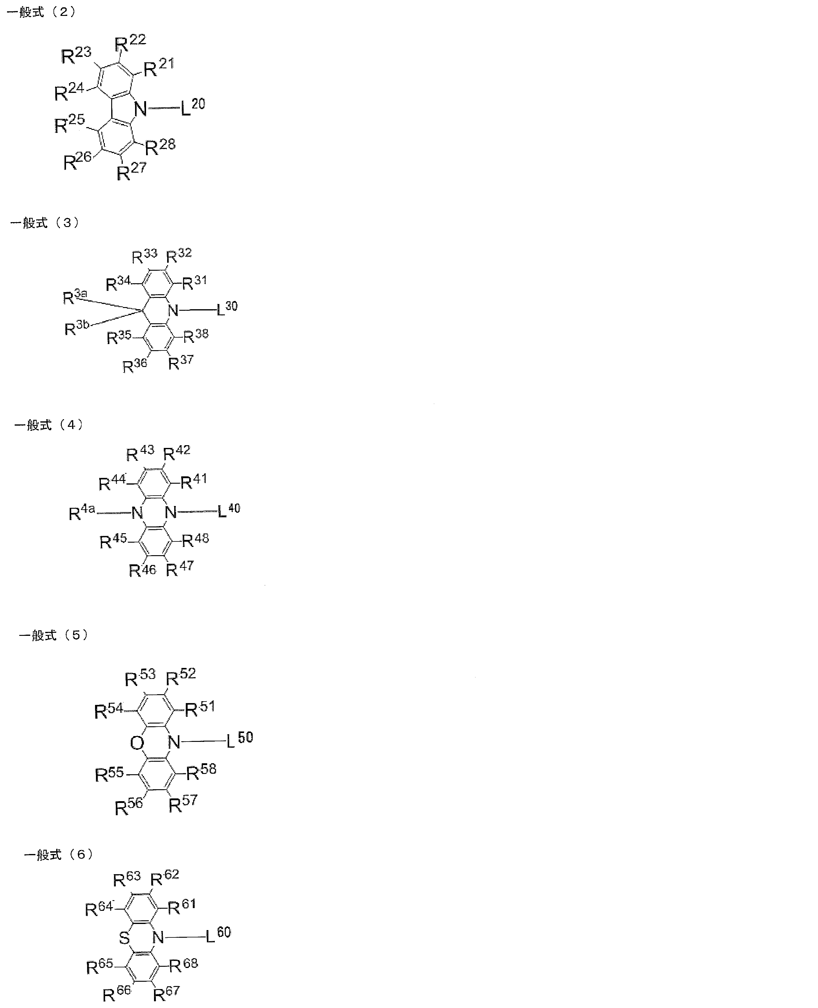
[2] 前記一般式(1)のR3またはR6のうちの少なくとも1つが、前記一般式(2)~(6)のいずれかで表される基であることを特徴とする[1]に記載の発光材料。
[3] 前記一般式(1)のR3とR6が、前記一般式(2)~(6)のいずれかで表される基であることを特徴とする[2]に記載の発光材料。
[4] 前記一般式(1)のR3またはR6のうちの少なくとも1つが、前記一般式(3)で表される基であることを特徴とする[2]に記載の発光材料。
[5] 前記一般式(1)のR3またはR6のうちの少なくとも1つが、前記一般式(2)で表される基であることを特徴とする[2]に記載の発光材料。
[6] 前記一般式(2)~(6)のR21~R28、R31~R38、R41~R48、R51~R58、R61~R68の少なくとも1つが、置換基であることを特徴とする[1]~[5]のいずれか1項に記載の発光材料。
[7] 前記一般式(2)~(6)のR23、R26、R33、R36、R43、R46、R53、R56、R63、R66の少なくとも1つが、置換基であることを特徴とする[6]に記載の発光材料。
[8] 前記置換基が、前記一般式(2)~(6)のいずれかで表される基であることを特徴とする[7]に記載の発光材料。
[9] 前記一般式(2)~(6)のLが、単結合であることを特徴とする[1]~[8]のいずれか1項に記載の発光材料。
[10] 前記一般式(1)のXが、酸素原子であることを特徴とする[1]~[9]のいずれか1項に記載の発光材料。
[11] 下記一般式(1)で表される化合物からなる遅延蛍光体。
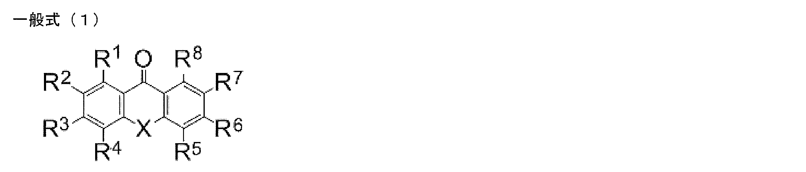
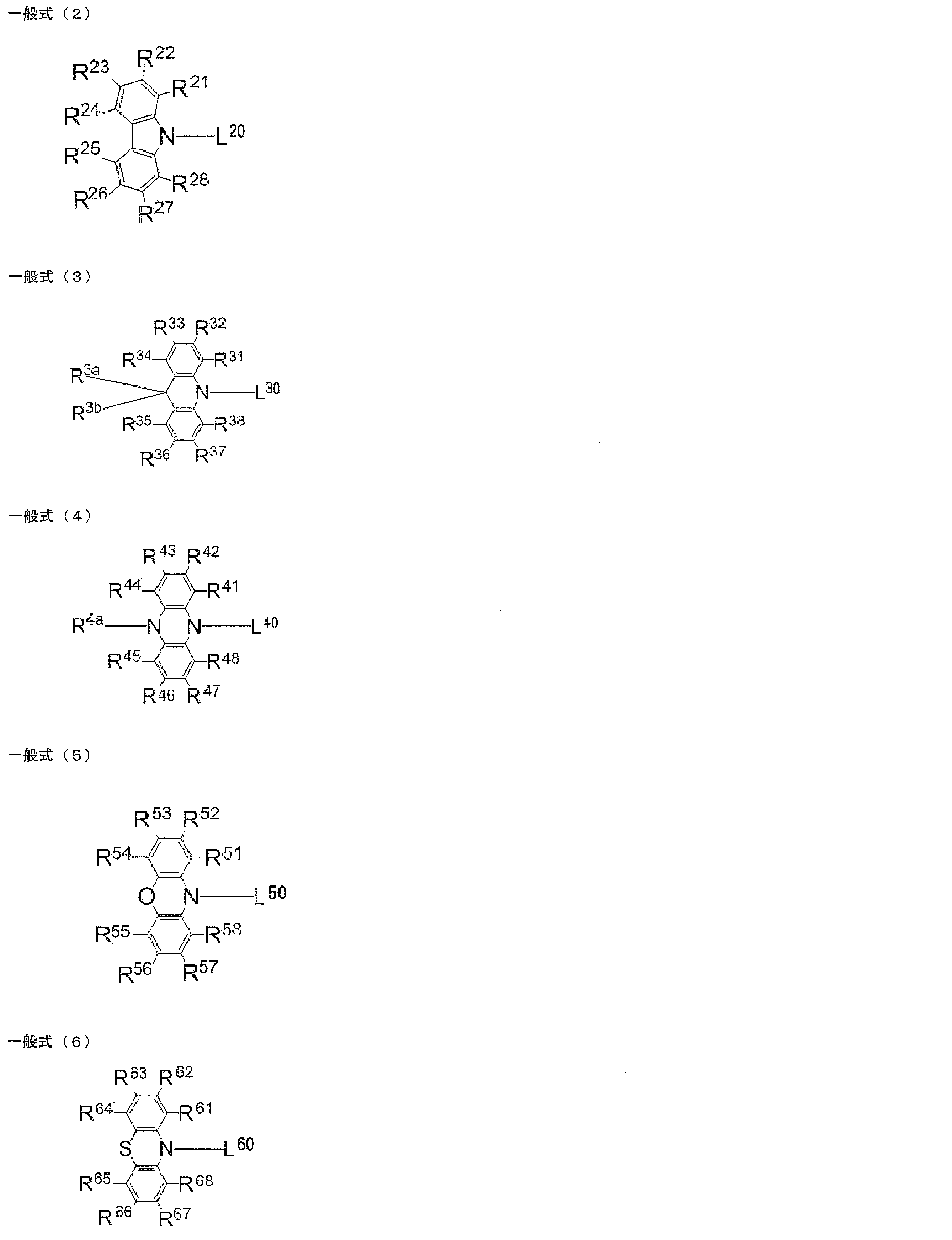
[12] [1]~[10]のいずれか1項に記載の発光材料を含むことを特徴とする有機発光素子。
[13] 遅延蛍光を放射することを特徴とする[12]に記載の有機発光素子。
[14] 有機エレクトロルミネッセンス素子であることを特徴とする[12]または[13]に記載の有機発光素子。
[15] 下記一般式(1’)で表される化合物。


本発明の発光材料は、下記一般式(1)で表される化合物からなることを特徴とする。
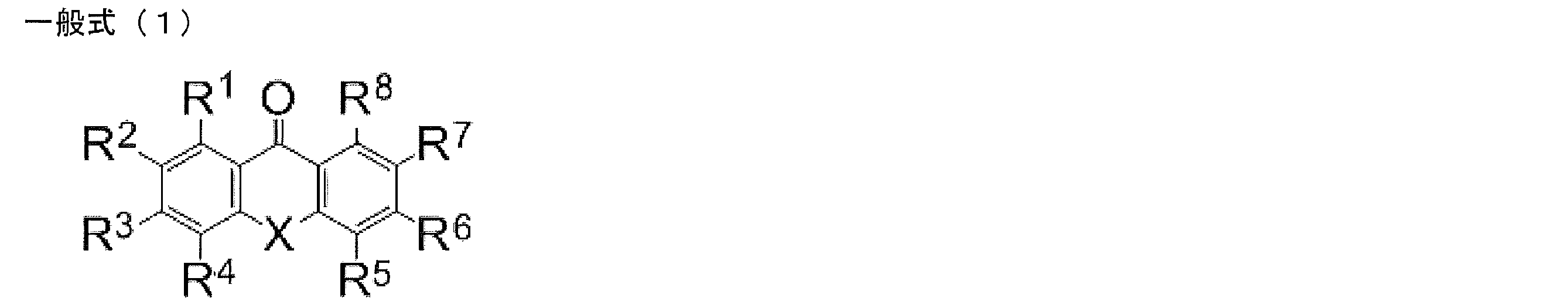
R1~R8のうち下記一般式(2)~(6)のいずれかで表される基は、1つのみであってもよいし、2つ以上であってもよいが、1~4つであることが好ましく、1つまたは2つであることがより好ましい。一般式(1)中に複数の一般式(2)~(6)で表される基が存在する場合、それらの基は同一であっても異なっていてもよい。
下記一般式(2)~(6)のいずれかで表される基がR1~R8のうちの1つのみであるときは、R2またはR3が下記一般式(2)~(6)のいずれかで表される基であることが好ましく、R3が下記一般式(2)~(6)のいずれかで表される基であることがより好ましい。
一方、R1~R8のうちの2つ以上が下記一般式(2)~(6)のいずれかで表される基であるときは、下記一般式(2)~(6)のいずれかで表される基は、R1~R4の少なくとも1つと、R5~R8の少なくとも1つであることが好ましい。このとき、下記一般式(2)~(6)のいずれかで表される基は、R1~R4のうちの1~3つ、R5~R8のうちの1~3つであることが好ましく、R1~R4のうちの1または2つ、R5~R8のうちの1または2つであることがより好ましい。R1~R4のうち一般式(2)~(6)のいずれかで表される基の数と、R5~R8のうち一般式(2)~(6)のいずれかで表される基の数は同じであっても異なっていてもよいが、同じであることが好ましい。R1~R4のうちでは、R2~R4の少なくとも1つが一般式(2)~(6)のいずれかで表される基であることが好ましく、少なくともR3が一般式(2)~(6)のいずれかで表される基であることがより好ましい。また、R5~R8のうちでは、R5~R7の少なくとも1つが一般式(2)~(6)のいずれかで表される基であることが好ましく、少なくともR6が一般式(2)~(6)のいずれかで表される基であることがより好ましい。好ましい化合物は、一般式(1)のR3とR6が一般式(2)~(6)のいずれかで表される基である化合物、一般式(1)のR2とR7が一般式(2)~(6)のいずれかで表される基である化合物、一般式(1)のR2、R3、R6、R7が一般式(2)~(6)のいずれかで表される基である化合物であり、さらに好ましい化合物はR3とR6が一般式(2)~(6)のいずれかで表される基である化合物である。一般式(1)中に存在する複数の一般式(2)~(6)のいずれかで表される基は、同一であっても異なっていてもよいが、同一であることが好ましい。また、一般式(1)で表される基は対称構造をとっていることも好ましい。すなわち、R1とR8、R2とR7、R3とR6、R4とR5は、それぞれ同一であることが好ましい。
一般式(1)の化合物は、R3とR6の両方が下記一般式(2)~(6)のいずれかで表される基であることがより好ましい。好ましい化合物は、一般式(1)のR3またはR6の少なくとも1つが下記一般式(2)または(3)で表される基である化合物である。

L20,L30,L40、L50,L60は、単結合であっても二価の連結基であってもよいが、単結合であることが好ましい。一般式(1)のR1~R8の少なくとも1つが、L20,L30,L40、L50,L60が連結基である一般式(2)~(6)で表される基であるとき、一般式(1)に存在する連結基の数は、1つのみであってもよいし、2つ以上であってもよい。一般式(1)中に複数の連結基が存在する場合、それらの連結基は同一であっても異なっていてもよい。L20,L30,L40、L50,L60がとりうるニ価の連結基としては、例えば、アルケニレン基、アルキニレン基、アリーレン基、チオフェンジイル基、これらの組み合わせからなる連結基を挙げることができる。アルキレン基やアルケニレン基の炭素数は2~10であることが好ましく、2~6であることがより好ましく、2~4であることがさらに好ましい。また、アリーレン基の炭素数は6~10であることが好ましく、6であることがより好ましく、パラフェニレン基がさらにより好ましい。チオフェンジイル基として、3,4-チオフェンジイル基、2,5-チオフェンジイル基を挙げることができる。好ましい連結基の一般式として-(CRa=CRb)n-で表される連結基を挙げることができる。ここでRaおよびRbは、各々独立に水素原子またはアルキル基を表す。アルキル基の炭素数は1~6であることが好ましく、1~3であることがより好ましい。nは1~5であることが好ましく、1~3であることがより好ましく、1または2であることがさらに好ましい。例えば、-CH=CH-や-(CH=CH)2-を挙げることができる。
R21~R28、R31~R38、R3a、R3b、R41~R48、R4a、R51~R58、R61~R68がとりうる置換基と、R1~R8とりうる置換基として、例えばヒドロキシ基、ハロゲン原子、シアノ基、炭素数1~20のアルキル基、炭素数1~20のアルコキシ基、炭素数1~20のアルキルチオ基、炭素数1~20のアルキル置換アミノ基、炭素数2~20のアシル基、炭素数6~40のアリール基、炭素数3~40のヘテロアリール基、炭素数2~10のアルケニル基、炭素数2~10のアルキニル基、炭素数2~10のアルコキシカルボニル基、炭素数1~10のアルキルスルホニル基、炭素数1~10のハロアルキル基、アミド基、炭素数2~10のアルキルアミド基、炭素数3~20のトリアルキルシリル基、炭素数4~20のトリアルキルシリルアルキル基、炭素数5~20のトリアルキルシリルアルケニル基、炭素数5~20のトリアルキルシリルアルキニル基およびニトロ基等が挙げられる。これらの具体例のうち、さらに置換基により置換可能なものは置換されていてもよい。より好ましい置換基は、ハロゲン原子、シアノ基、炭素数1~20の置換もしくは無置換のアルキル基、炭素数1~20のアルコキシ基、炭素数6~40の置換もしくは無置換のアリール基、炭素数3~40の置換もしくは無置換のヘテロアリール基、炭素数1~20のジアルキル置換アミノ基である。さらに好ましい置換基は、フッ素原子、塩素原子、シアノ基、炭素数1~10の置換もしくは無置換のアルキル基、炭素数1~10の置換もしくは無置換のアルコキシ基、炭素数6~15の置換もしくは無置換のアリール基、炭素数3~12の置換もしくは無置換のヘテロアリール基である。
また、R23、R26、R33、R36、R43、R46、R53、R56、R63、R66の少なくとも1つは、各々独立に上記一般式(2)~(6)のいずれかで表される基であることが好ましい。
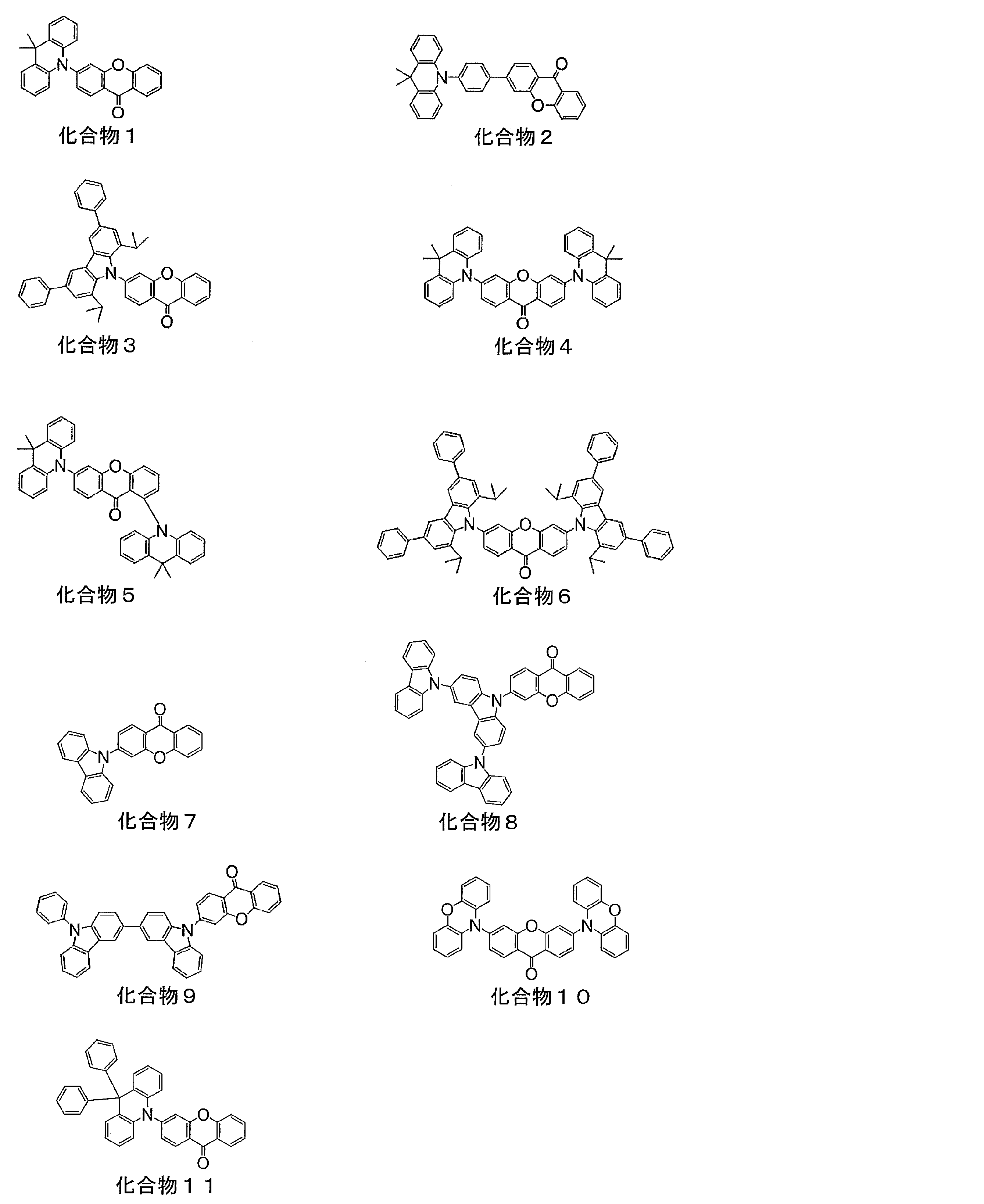
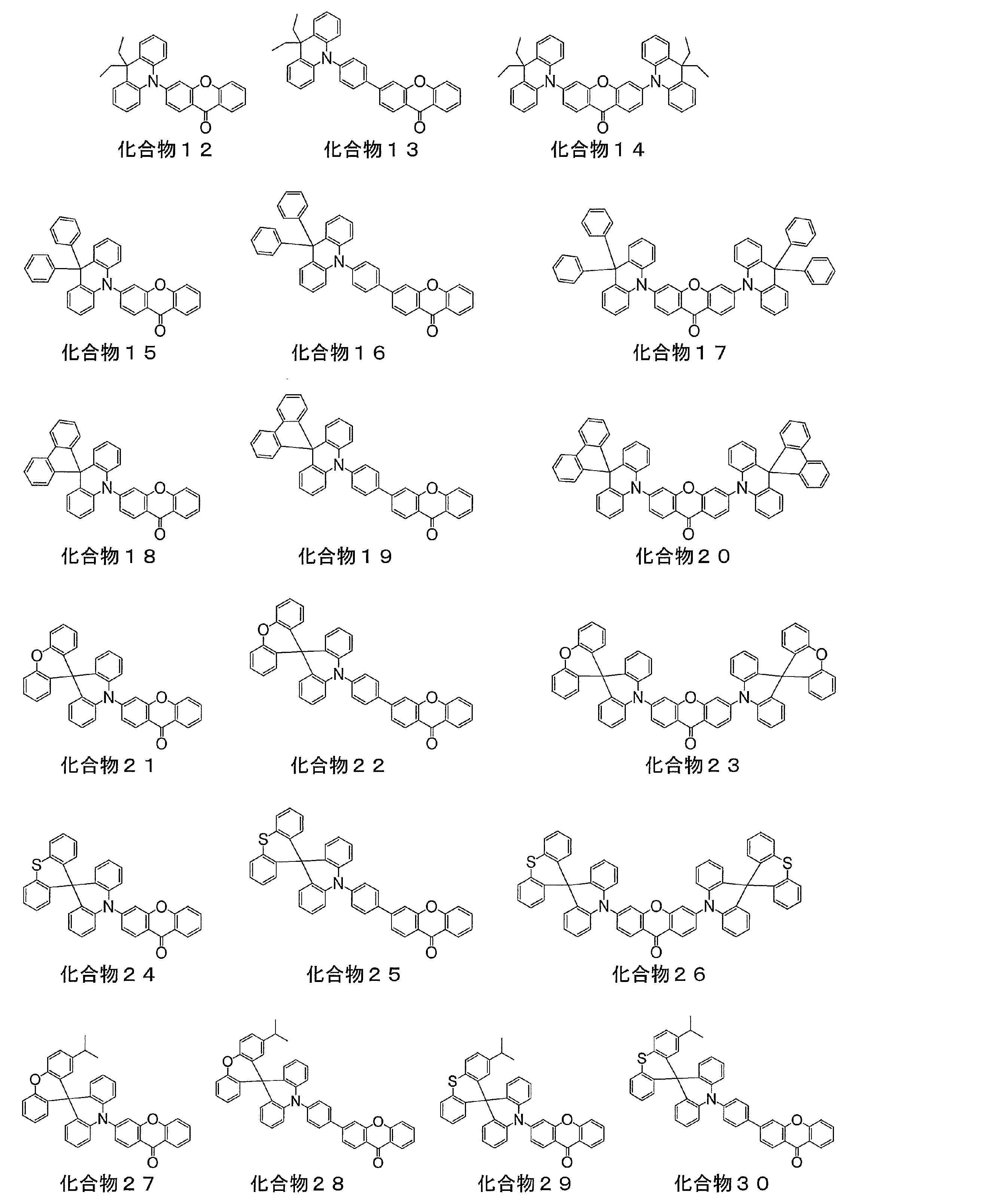

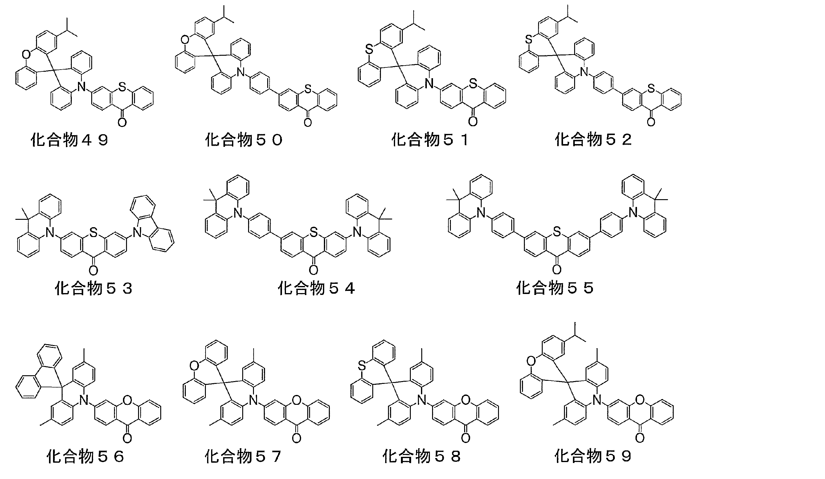
一般式(1)で表される化合物は、分子量にかかわらず塗布法で成膜してもよい。塗布法を用いれば、分子量が比較的大きな化合物であっても成膜することが可能である。
例えば、一般式(1)で表される構造中にあらかじめ重合性基を存在させておいて、その重合性基を重合させることによって得られる重合体を、発光材料として用いることが考えられる。具体的には、一般式(1)のR1~R8のいずれかに重合性官能基を含むモノマーを用意して、これを単独で重合させるか、他のモノマーとともに共重合させることにより、繰り返し単位を有する重合体を得て、その重合体を発光材料として用いることが考えられる。あるいは、一般式(1)で表される構造を有する化合物どうしをカップリングさせることにより、二量体や三量体を得て、それらを発光材料として用いることも考えられる。

一般式(9)または(10)において、R101、R102、R103およびR104は、各々独立に置換基を表す。好ましくは、炭素数1~6の置換もしくは無置換のアルキル基、炭素数1~6の置換もしくは無置換のアルコキシ基、ハロゲン原子であり、より好ましくは炭素数1~3の無置換のアルキル基、炭素数1~3の無置換のアルコキシ基、フッ素原子、塩素原子であり、さらに好ましくは炭素数1~3の無置換のアルキル基、炭素数1~3の無置換のアルコキシ基である。
L1およびL2で表される連結基は、Qを構成する一般式(1)の構造のR1~R8のいずれか、一般式(2)のR21~R28のいずれか、一般式(3)の構造のR31~R38、R3a、R3bのいずれか、一般式(4)の構造のR41~R48、R4aのいずれか、一般式(5)の構造のR51~R58のいずれか、一般式(6)の構造のR61~R68のいずれかに結合することができる。1つのQに対して連結基が2つ以上連結して架橋構造や網目構造を形成していてもよい。


一般式(1)で表される化合物のうち、下記一般式(1’)で表される化合物は新規化合物である。


一般式(1’)におけるR1’~R8’、R21’~R28’、R31’~R38’、R3a’、R3b’、R41’~R48’、R4a’、R51’~R58’、R61’~R68’の説明と好ましい範囲については、一般式(1)で表される化合物の説明を参照することができる。ただし、R2’とR7’が下記一般式(2)で表される基であり、且つ、R21’~R28’が全て水素原子である場合を除く。R2’とR7’がともに置換されている場合として、一般式(3’)~(6’)のいずれかで表される基により置換されている化合物を挙げることができる。
一般式(1’)で表される化合物は、既知の反応を組み合わせることによって合成することができる。例えば、一般式(1’)のR3’、R6’が一般式(3’)で表される基である化合物は、以下の2つの化合物を反応させることにより合成することが可能である。
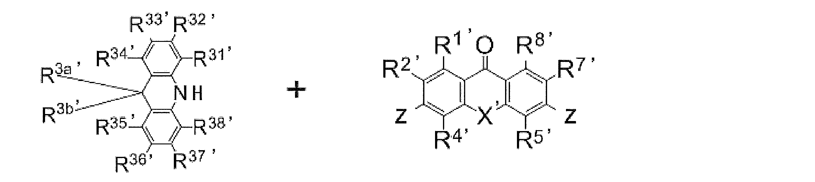
上記の反応は、公知のカップリング反応を応用したものであり、公知の反応条件を適宜選択して用いることができる。上記の反応の詳細については、後述の合成例を参考にすることができる。また、一般式(1’)で表される化合物は、その他の公知の合成反応を組み合わせることによっても合成することができる。
本発明の一般式(1)で表される化合物は、有機発光素子の発光材料として有用である。このため、本発明の一般式(1)で表される化合物は、有機発光素子の発光層に発光材料として効果的に用いることができる。一般式(1)で表される化合物の中には、遅延蛍光を放射する遅延蛍光材料(遅延蛍光体)が含まれている。すなわち本発明は、一般式(1)で表される構造を有する遅延蛍光体の発明と、一般式(1)で表される化合物を遅延蛍光体として使用する発明と、一般式(1)で表される化合物を用いて遅延蛍光を発光させる方法の発明も提供する。そのような化合物を発光材料として用いた有機発光素子は、遅延蛍光を放射し、発光効率が高いという特徴を有する。その原理を、有機エレクトロルミネッセンス素子を例にとって説明すると以下のようになる。
有機フォトルミネッセンス素子は、基板上に少なくとも発光層を形成した構造を有する。また、有機エレクトロルミネッセンス素子は、少なくとも陽極、陰極、および陽極と陰極の間に有機層を形成した構造を有する。有機層は、少なくとも発光層を含むものであり、発光層のみからなるものであってもよいし、発光層の他に1層以上の有機層を有するものであってもよい。そのような他の有機層として、正孔輸送層、正孔注入層、電子阻止層、正孔阻止層、電子注入層、電子輸送層、励起子阻止層などを挙げることができる。正孔輸送層は正孔注入機能を有した正孔注入輸送層でもよく、電子輸送層は電子注入機能を有した電子注入輸送層でもよい。具体的な有機エレクトロルミネッセンス素子の構造例を図1に示す。図1において、1は基板、2は陽極、3は正孔注入層、4は正孔輸送層、5は発光層、6は電子輸送層、7は陰極を表わす。
以下において、有機エレクトロルミネッセンス素子の各部材および各層について説明する。なお、基板と発光層の説明は有機フォトルミネッセンス素子の基板と発光層にも該当する。
本発明の有機エレクトロルミネッセンス素子は、基板に支持されていることが好ましい。この基板については、特に制限はなく、従来から有機エレクトロルミネッセンス素子に慣用されているものであればよく、例えば、ガラス、透明プラスチック、石英、シリコンなどからなるものを用いることができる。
有機エレクトロルミネッセンス素子における陽極としては、仕事関数の大きい(4eV以上)金属、合金、電気伝導性化合物およびこれらの混合物を電極材料とするものが好ましく用いられる。このような電極材料の具体例としてはAu等の金属、CuI、インジウムチンオキシド(ITO)、SnO2、ZnO等の導電性透明材料が挙げられる。また、IDIXO(In2O3-ZnO)等非晶質で透明導電膜を作製可能な材料を用いてもよい。陽極はこれらの電極材料を蒸着やスパッタリング等の方法により、薄膜を形成させ、フォトリソグラフィー法で所望の形状のパターンを形成してもよく、あるいはパターン精度をあまり必要としない場合は(100μm以上程度)、上記電極材料の蒸着やスパッタリング時に所望の形状のマスクを介してパターンを形成してもよい。あるいは、有機導電性化合物のように塗布可能な材料を用いる場合には、印刷方式、コーティング方式等湿式成膜法を用いることもできる。この陽極より発光を取り出す場合には、透過率を10%より大きくすることが望ましく、また陽極としてのシート抵抗は数百Ω/□以下が好ましい。さらに膜厚は材料にもよるが、通常10~1000nm、好ましくは10~200nmの範囲で選ばれる。
一方、陰極としては、仕事関数の小さい(4eV以下)金属(電子注入性金属と称する)、合金、電気伝導性化合物およびこれらの混合物を電極材料とするものが用いられる。このような電極材料の具体例としては、ナトリウム、ナトリウム-カリウム合金、マグネシウム、リチウム、マグネシウム/銅混合物、マグネシウム/銀混合物、マグネシウム/アルミニウム混合物、マグネシウム/インジウム混合物、アルミニウム/酸化アルミニウム(Al2O3)混合物、インジウム、リチウム/アルミニウム混合物、希土類金属等が挙げられる。これらの中で、電子注入性および酸化等に対する耐久性の点から、電子注入性金属とこれより仕事関数の値が大きく安定な金属である第二金属との混合物、例えば、マグネシウム/銀混合物、マグネシウム/アルミニウム混合物、マグネシウム/インジウム混合物、アルミニウム/酸化アルミニウム(Al2O3)混合物、リチウム/アルミニウム混合物、アルミニウム等が好適である。陰極はこれらの電極材料を蒸着やスパッタリング等の方法により薄膜を形成させることにより、作製することができる。また、陰極としてのシート抵抗は数百Ω/□以下が好ましく、膜厚は通常10nm~5μm、好ましくは50~200nmの範囲で選ばれる。なお、発光した光を透過させるため、有機エレクトロルミネッセンス素子の陽極または陰極のいずれか一方が、透明または半透明であれば発光輝度が向上し好都合である。
また、陽極の説明で挙げた導電性透明材料を陰極に用いることで、透明または半透明の陰極を作製することができ、これを応用することで陽極と陰極の両方が透過性を有する素子を作製することができる。
発光層は、陽極および陰極のそれぞれから注入された正孔および電子が再結合することにより励起子が生成した後、発光する層であり、発光材料を単独で発光層に使用しても良いが、好ましくは発光材料とホスト材料を含む。発光材料としては、一般式(1)で表される本発明の化合物群から選ばれる1種または2種以上を用いることができる。本発明の有機エレクトロルミネッセンス素子および有機フォトルミネッセンス素子が高い発光効率を発現するためには、発光材料に生成した一重項励起子および三重項励起子を、発光材料中に閉じ込めることが重要である。従って、発光層中に発光材料に加えてホスト材料を用いることが好ましい。ホスト材料としては、励起一重項エネルギー、励起三重項エネルギーの少なくとも何れか一方が本発明の発光材料よりも高い値を有する有機化合物を用いることができる。その結果、本発明の発光材料に生成した一重項励起子および三重項励起子を、本発明の発光材料の分子中に閉じ込めることが可能となり、その発光効率を十分に引き出すことが可能となる。もっとも、一重項励起子および三重項励起子を十分に閉じ込めることができなくても、高い発光効率を得ることが可能な場合もあるため、高い発光効率を実現しうるホスト材料であれば特に制約なく本発明に用いることができる。本発明の有機発光素子または有機エレクトロルミネッセンス素子において、発光は発光層に含まれる本発明の発光材料から生じる。この発光は蛍光発光および遅延蛍光発光の両方を含む。但し、発光の一部或いは部分的にホスト材料からの発光があってもかまわない。
ホスト材料を用いる場合、発光材料である本発明の化合物が発光層中に含有される量は0.1重量%以上であることが好ましく、1重量%以上であることがより好ましく、また、50重量%以下であることが好ましく、20重量%以下であることがより好ましく、10重量%以下であることがさらに好ましい。
発光層におけるホスト材料としては、正孔輸送能、電子輸送能を有し、かつ発光の長波長化を防ぎ、なおかつ高いガラス転移温度を有する有機化合物であることが好ましい。
注入層とは、駆動電圧低下や発光輝度向上のために電極と有機層間に設けられる層のことで、正孔注入層と電子注入層があり、陽極と発光層または正孔輸送層の間、および陰極と発光層または電子輸送層との間に存在させてもよい。注入層は必要に応じて設けることができる。
阻止層は、発光層中に存在する電荷(電子もしくは正孔)および/または励起子の発光層外への拡散を阻止することができる層である。電子阻止層は、発光層および正孔輸送層の間に配置されることができ、電子が正孔輸送層の方に向かって発光層を通過することを阻止する。同様に、正孔阻止層は発光層および電子輸送層の間に配置されることができ、正孔が電子輸送層の方に向かって発光層を通過することを阻止する。阻止層はまた、励起子が発光層の外側に拡散することを阻止するために用いることができる。すなわち電子阻止層、正孔阻止層はそれぞれ励起子阻止層としての機能も兼ね備えることができる。本明細書でいう電子阻止層または励起子阻止層は、一つの層で電子阻止層および励起子阻止層の機能を有する層を含む意味で使用される。
正孔阻止層とは広い意味では電子輸送層の機能を有する。正孔阻止層は電子を輸送しつつ、正孔が電子輸送層へ到達することを阻止する役割があり、これにより発光層中での電子と正孔の再結合確率を向上させることができる。正孔阻止層の材料としては、後述する電子輸送層の材料を必要に応じて用いることができる。
電子阻止層とは、広い意味では正孔を輸送する機能を有する。電子阻止層は正孔を輸送しつつ、電子が正孔輸送層へ到達することを阻止する役割があり、これにより発光層中での電子と正孔が再結合する確率を向上させることができる。
励起子阻止層とは、発光層内で正孔と電子が再結合することにより生じた励起子が電荷輸送層に拡散することを阻止するための層であり、本層の挿入により励起子を効率的に発光層内に閉じ込めることが可能となり、素子の発光効率を向上させることができる。励起子阻止層は発光層に隣接して陽極側、陰極側のいずれにも挿入することができ、両方同時に挿入することも可能である。すなわち、励起子阻止層を陽極側に有する場合、正孔輸送層と発光層の間に、発光層に隣接して該層を挿入することができ、陰極側に挿入する場合、発光層と陰極との間に、発光層に隣接して該層を挿入することができる。また、陽極と、発光層の陽極側に隣接する励起子阻止層との間には、正孔注入層や電子阻止層などを有することができ、陰極と、発光層の陰極側に隣接する励起子阻止層との間には、電子注入層、電子輸送層、正孔阻止層などを有することができる。阻止層を配置する場合、阻止層として用いる材料の励起一重項エネルギーおよび励起三重項エネルギーの少なくともいずれか一方は、発光材料の励起一重項エネルギーおよび励起三重項エネルギーよりも高いことが好ましい。
正孔輸送層とは正孔を輸送する機能を有する正孔輸送材料からなり、正孔輸送層は単層または複数層設けることができる。
正孔輸送材料としては、正孔の注入または輸送、電子の障壁性のいずれかを有するものであり、有機物、無機物のいずれであってもよい。使用できる公知の正孔輸送材料としては例えば、トリアゾール誘導体、オキサジアゾール誘導体、イミダゾール誘導体、カルバゾール誘導体、インドロカルバゾール誘導体、ポリアリールアルカン誘導体、ピラゾリン誘導体およびピラゾロン誘導体、フェニレンジアミン誘導体、アリールアミン誘導体、アミノ置換カルコン誘導体、オキサゾール誘導体、スチリルアントラセン誘導体、フルオレノン誘導体、ヒドラゾン誘導体、スチルベン誘導体、シラザン誘導体、アニリン系共重合体、また導電性高分子オリゴマー、特にチオフェンオリゴマー等が挙げられるが、ポルフィリン化合物、芳香族第3級アミン化合物およびスチリルアミン化合物を用いることが好ましく、芳香族第3級アミン化合物を用いることがより好ましい。
電子輸送層とは電子を輸送する機能を有する材料からなり、電子輸送層は単層または複数層設けることができる。
電子輸送材料(正孔阻止材料を兼ねる場合もある)としては、陰極より注入された電子を発光層に伝達する機能を有していればよい。使用できる電子輸送層としては例えば、ニトロ置換フルオレン誘導体、ジフェニルキノン誘導体、チオピランジオキシド誘導体、カルボジイミド、フレオレニリデンメタン誘導体、アントラキノジメタンおよびアントロン誘導体、オキサジアゾール誘導体等が挙げられる。さらに、上記オキサジアゾール誘導体において、オキサジアゾール環の酸素原子を硫黄原子に置換したチアジアゾール誘導体、電子吸引基として知られているキノキサリン環を有するキノキサリン誘導体も、電子輸送材料として用いることができる。さらにこれらの材料を高分子鎖に導入した、またはこれらの材料を高分子の主鎖とした高分子材料を用いることもできる。
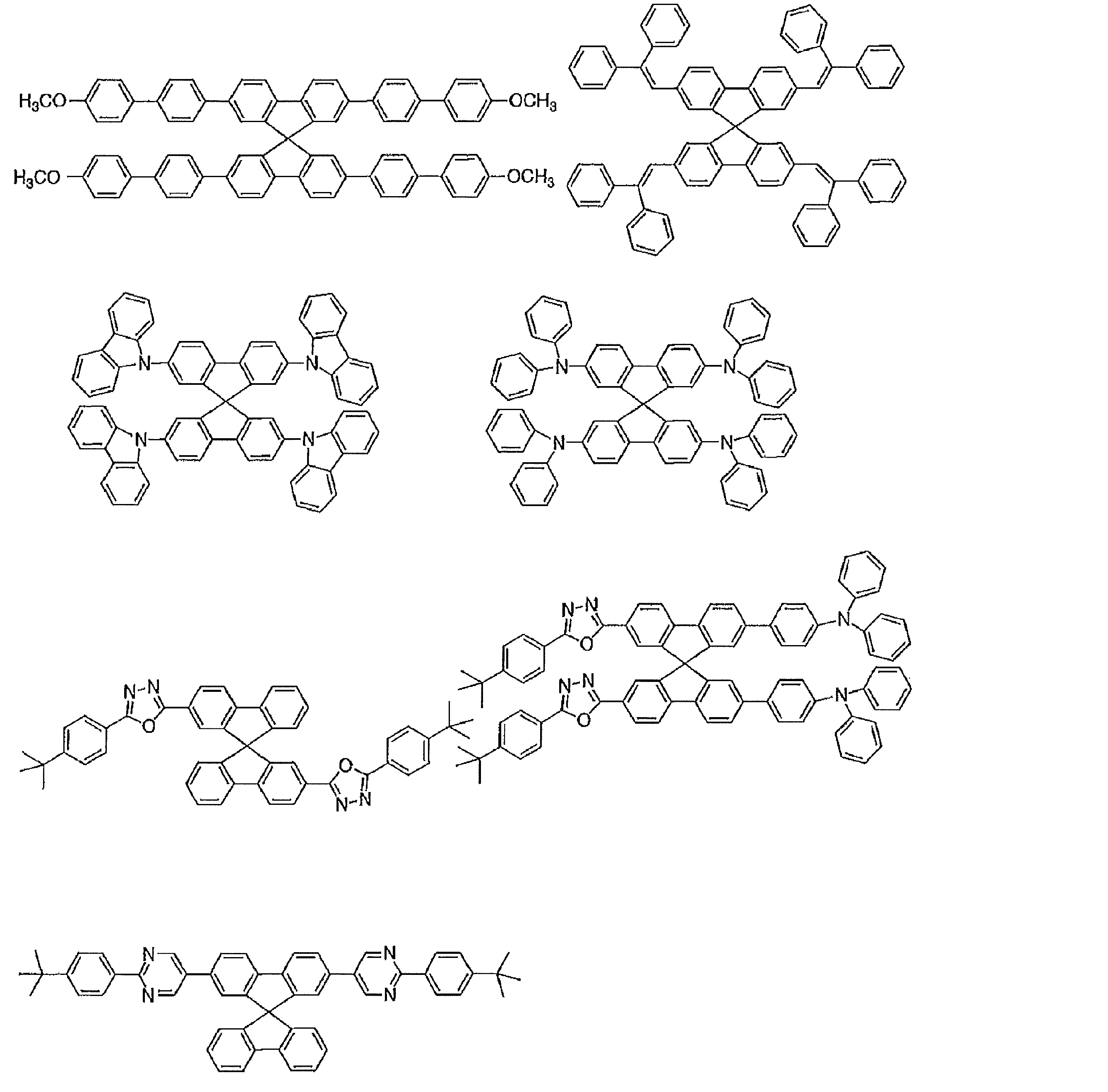


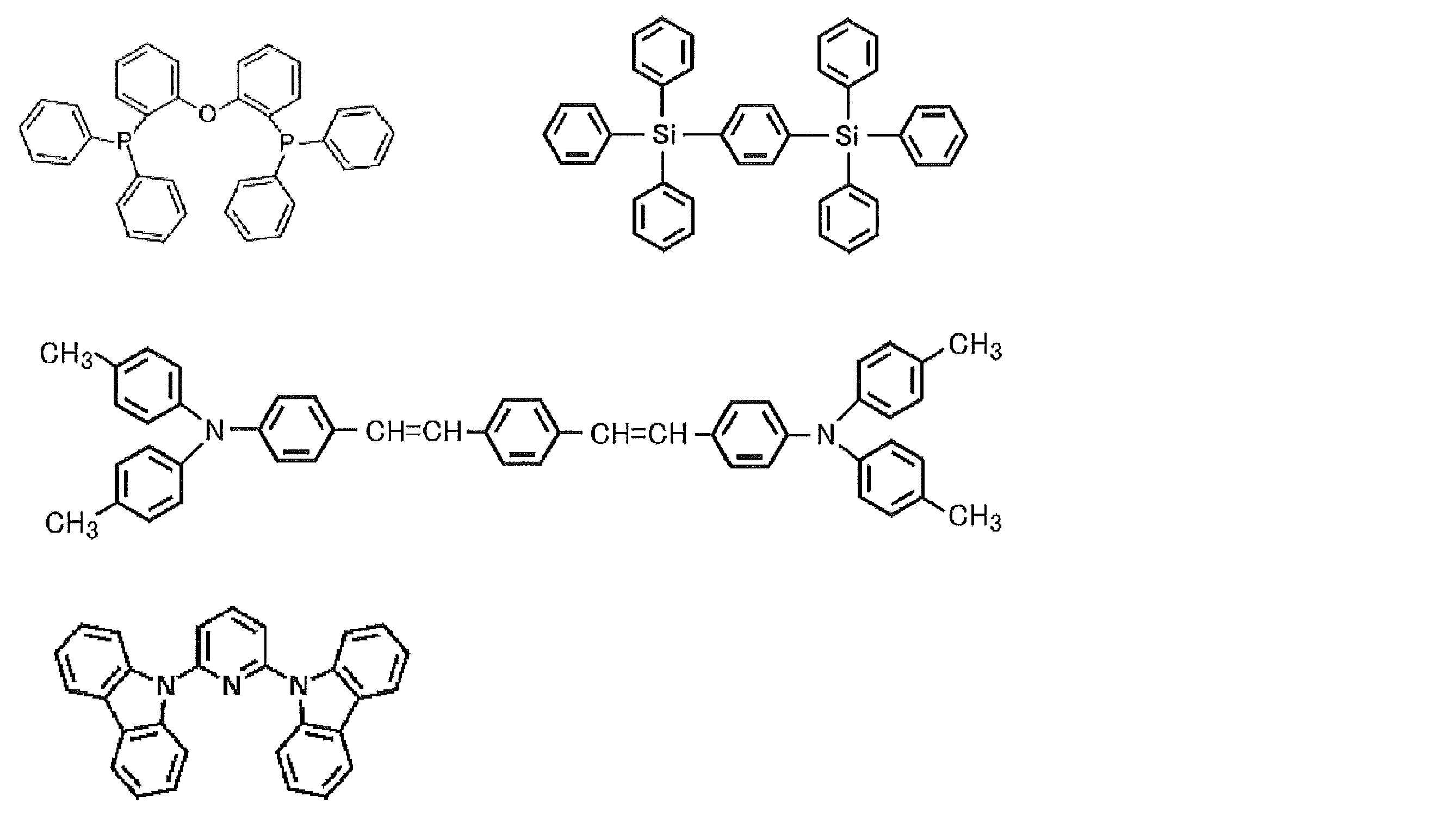
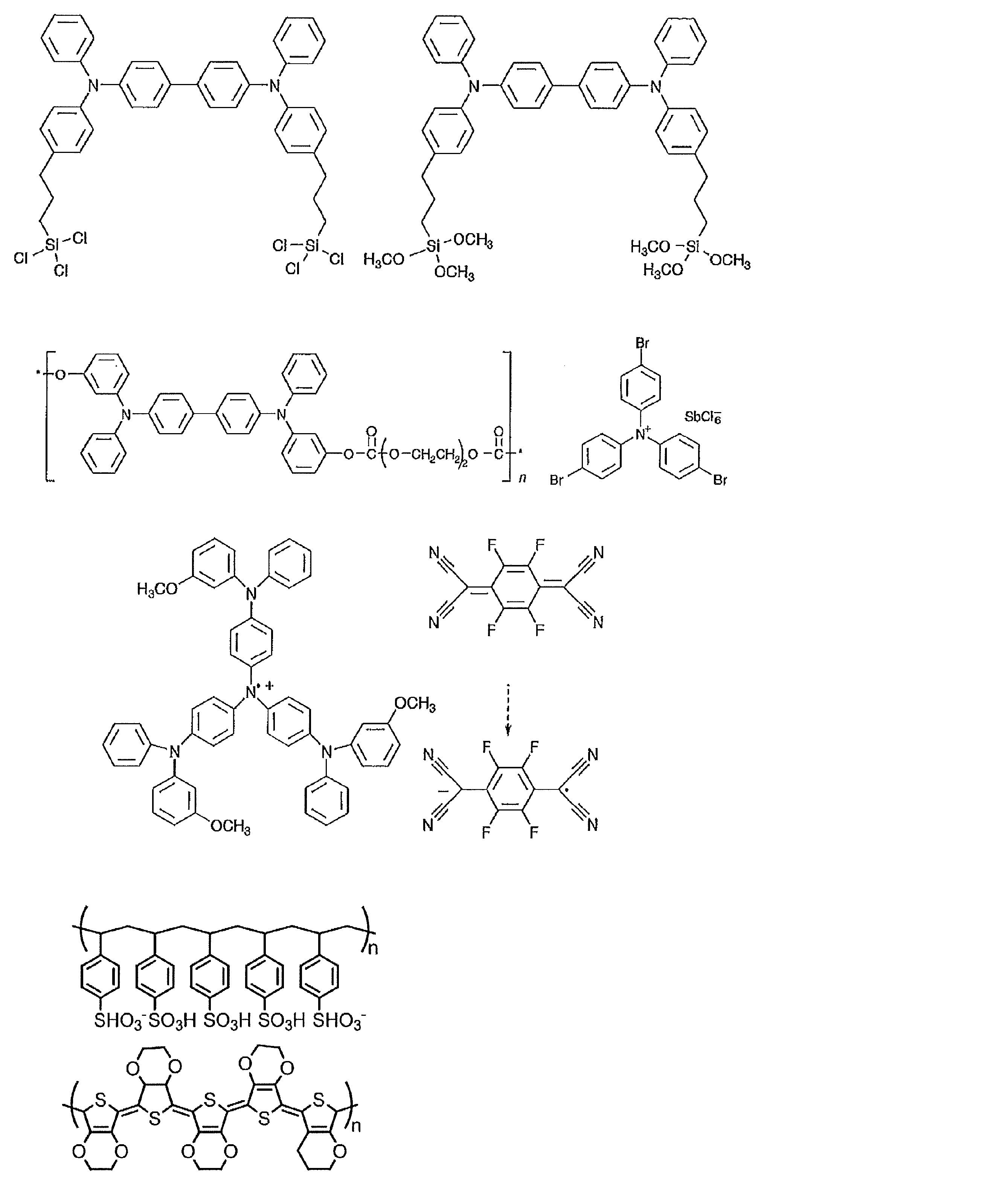
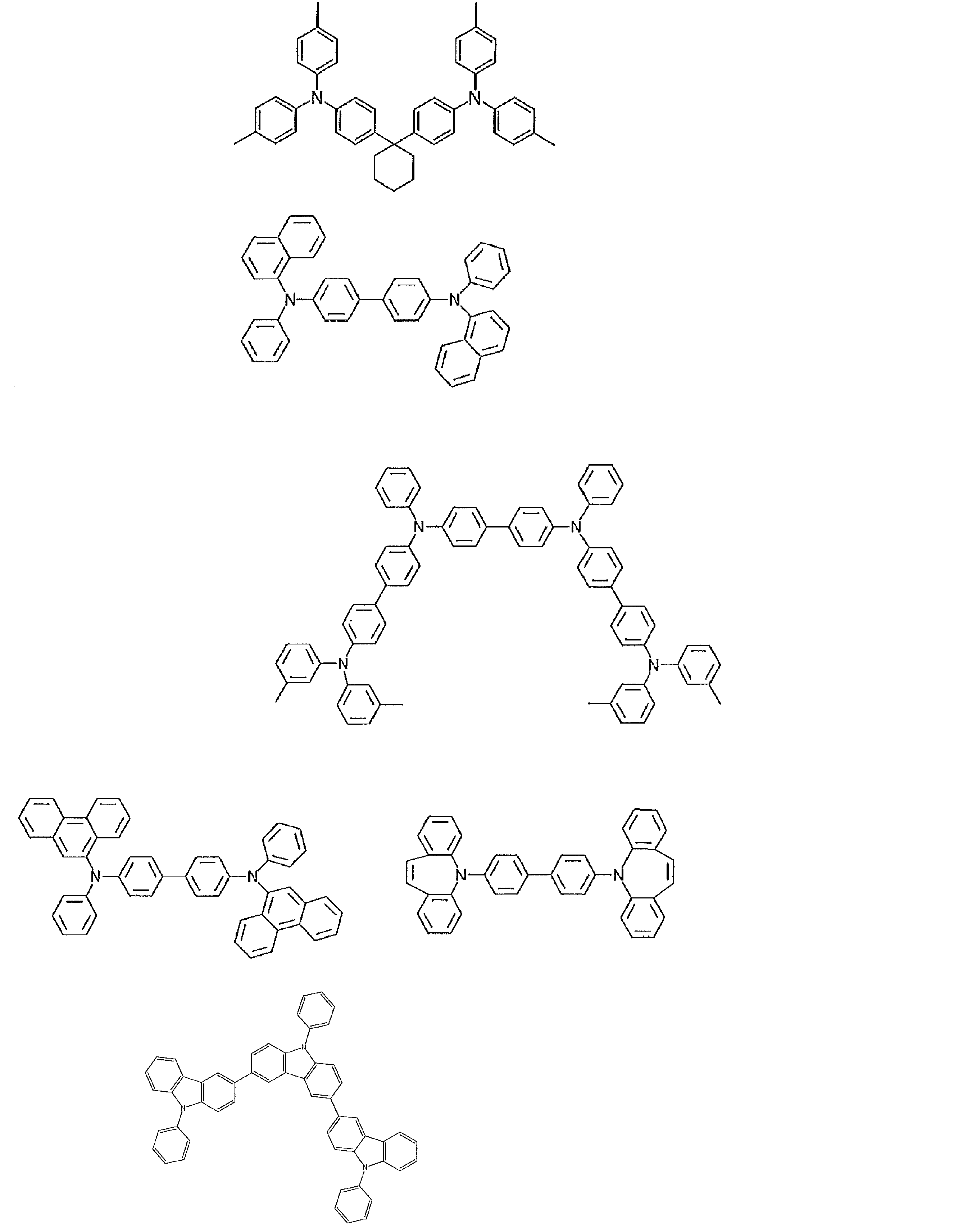
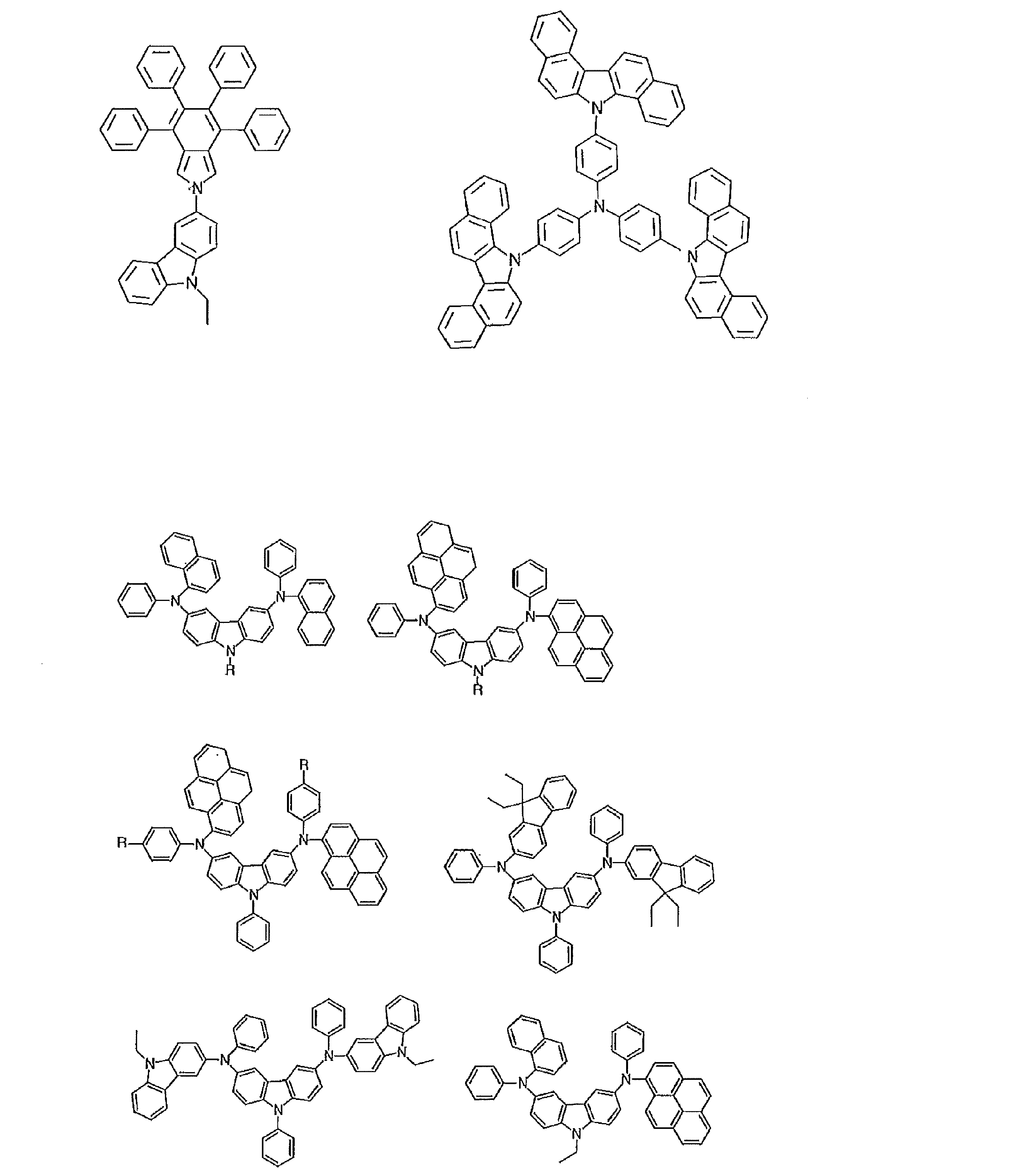


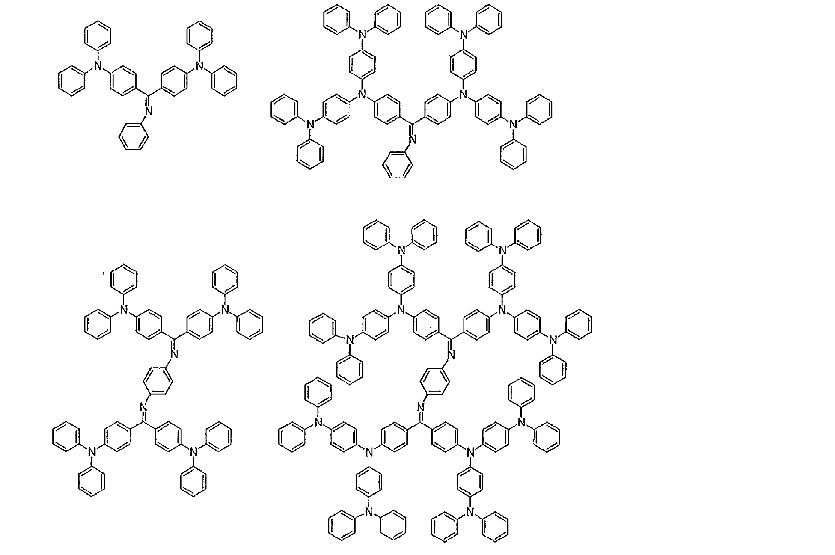
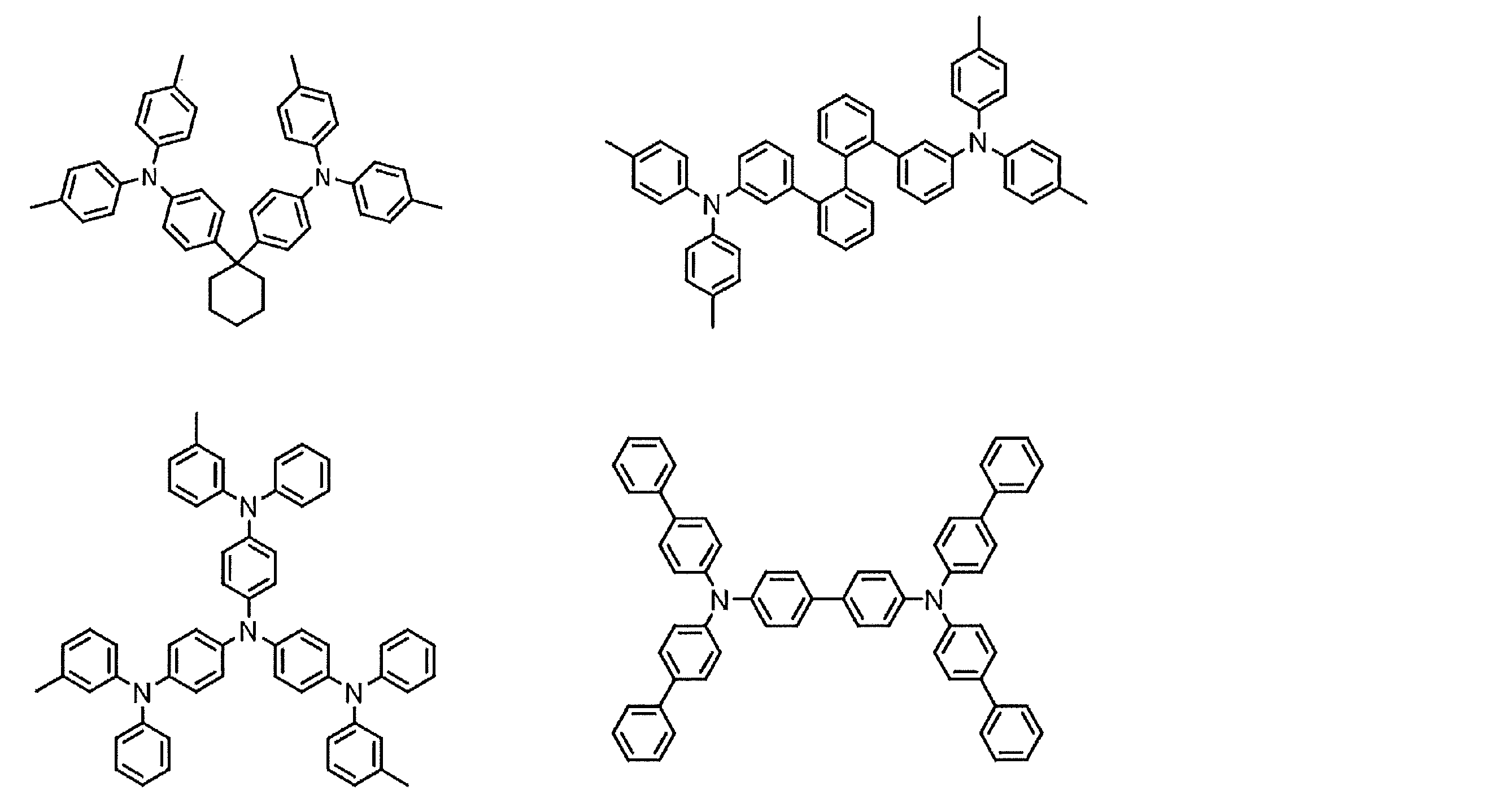


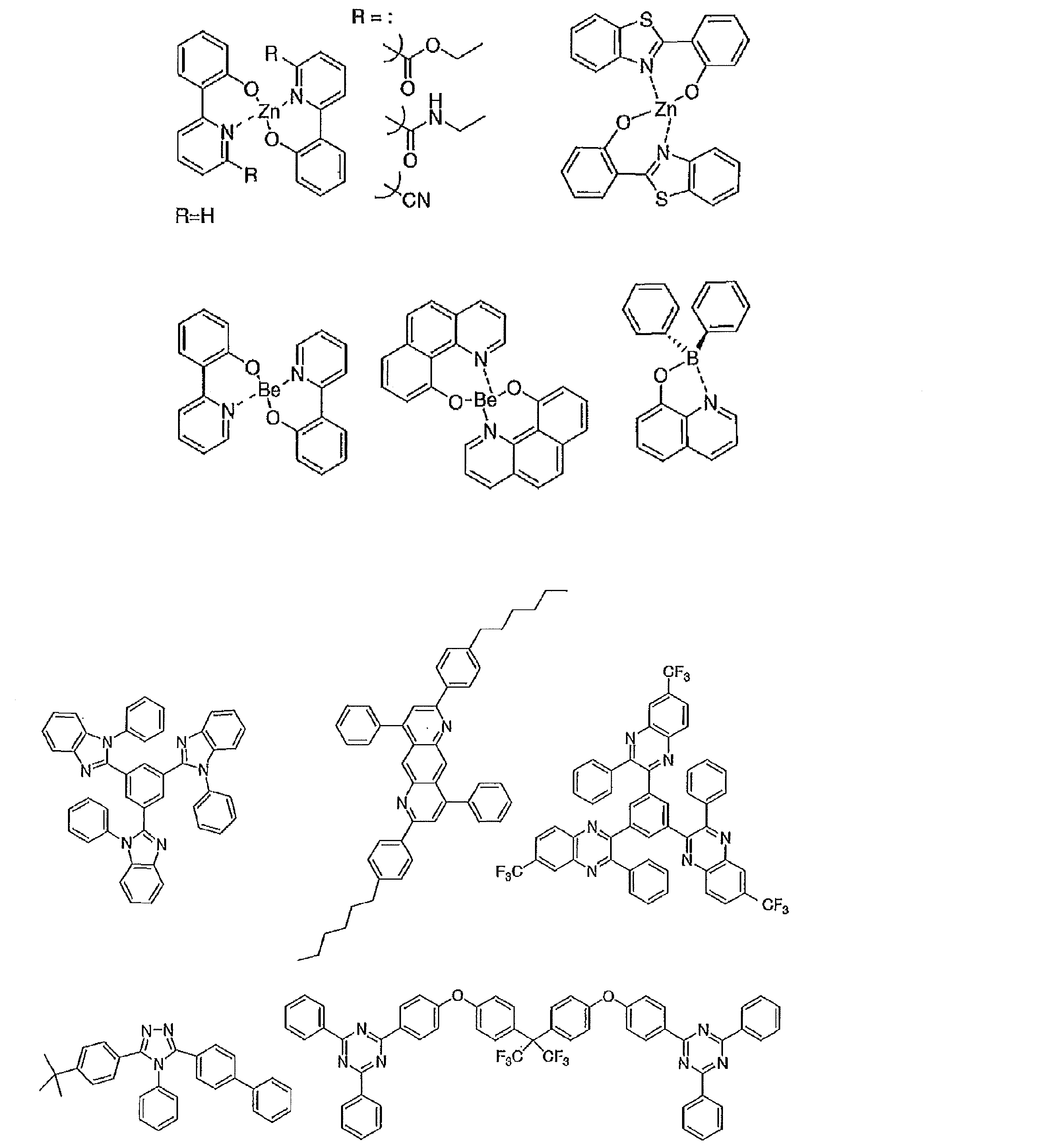


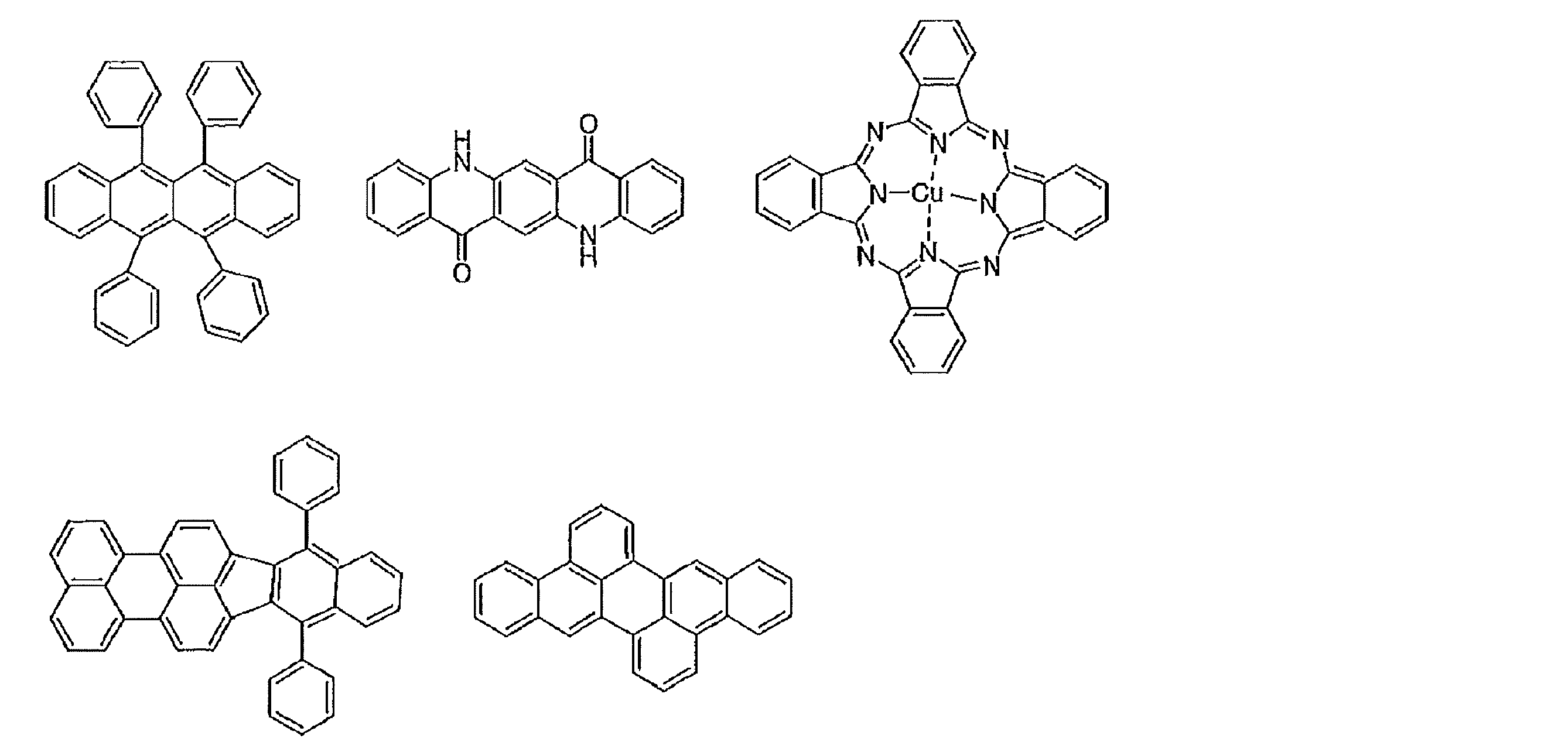
一方、りん光については、本発明の化合物のような通常の有機化合物では、励起三重項エネルギーは不安定で熱等に変換され、寿命が短く直ちに失活するため、室温では殆ど観測できない。通常の有機化合物の励起三重項エネルギーを測定するためには、極低温の条件での発光を観測することにより測定可能である。
以下の手順にしたがって化合物1を合成した。
室温に戻した後に4-ブロモ-2-フルオロベンゾニトリル(25.0g,125mmol)を加え、窒素雰囲気下で4時間還流させた。反応終了後、溶液にトルエン(200ml)を加えて希釈し、セライトを通して濾過した。これを分液ロートで二回水洗し、無水硫酸マグネシウムで乾燥し、濾過した。これをシリカゲルクロマトグラフィー(移動相トルエン:酢酸エチル=9:1)で精製し、濃縮により析出した試料をヘキサン200mlで超音波洗浄を5分間行い、ろ取した。これを真空乾燥(50℃、4時間)し、白色の固体を得た(収量31.2g、収率91%)。同定は1H-NMRとESI-MSにより行った。
1H NMR(500MHz,CDCl3,δ):6.97(s,1H),7.11(d,2H),7.25-7.31(m,2H),7.42-7.48(m,2H),7.51(d,1H)
ESI-MS(m/z)(M+):calcd 272.98 found 273.09

1H-NMR(500MHz,CDCl3,δ):7.41(t,1H),7.46-7.54(m,2H),7.71(s,1H),7.75(t,1H),8.20(d,1H) 8.33(d,1H)
ESI-MS(m/z)(M+):calcd 273.96 found 274.08

1H-NMR(500MHz,CDCl3,δ):1.68(s,6H),6.53(d,2H),6.96-7.08(m, 4H),7.38(d,1H),7.42(t,1H),7.46-7.52(m,3H),7.53(s,1H),7.74(t,1H)8.38(d,1H) 8.53(d,1H)
ESI-MS(m/z)(M+):calcd 403.16 found 403.23
以下の手順にしたがって化合物4を合成した。

室温に戻した後に4-ブロモ-2-フルオロベンゾニトリル(25.0g,125mmol)を加え、窒素雰囲気下で4時間還流させた。反応終了後、溶液にトルエン(200ml)を加えて希釈し、セライトを通して濾過した。これを分液ロートで二回水洗し、無水硫酸マグネシウムで乾燥し、濾過した。これをシリカゲルクロマトグラフィー(移動相トルエン:酢酸エチル=9:1)で精製し、濃縮により析出した試料をヘキサン(200ml)で超音波洗浄を5分間行い、ろ取した。これを真空乾燥(50℃、4時間)し、白色の固体を得た(収量43.8g、収率99%)。同定は1H-NMRとESI-MSにより行った。
1H-NMR(500MHz,CDCl3,δ):7.02(d,1H),7.05(d,1H),7.27(t,1H),7.29-7.35(m、2H),7.41(d,1H),7.53(d,1H)
ESI-MS(m/z)(M+):calcd 350.89 found 351.04

化合物2b:
1H-NMR(500MHz,CDCl3,δ):7.52(d,2H),7.69(s,2H),8.07(d,2H)
ESI-MS(m/z)(M+):calcd 351.87 found 351.53
化合物2c:
1H-NMR(500MHz,CDCl3,δ):7.44-7.54(m,3H),7.65(dd,2H),8.17(d,1H)
ESI-MS(m/z)(M+):calcd 351.87 found 351.53

1H-NMR(500MHz,CDCl3,δ):1.69(s,12H),6.57(d,4H),6.98-7.11(m,8H),7.41(d,2H),7.47-7.55(m,6H),8.57(d,2H)
ESI-MS(m/z)(M+):calcd 610.26 found 610.27
下記の反応式にしたがって、合成例1の化合物1と同様にして合成した(収率97%)。

反応終了後、分液ロートを用いてジクロロメタンで抽出を行い、無水硫酸マグネシウムで乾燥後、濾過、濃縮した。これをシリカゲルカラムクロマトグラフィー(移動相:ジクロロメタン)で精製した。さらにこれを酢酸エチル:n-ヘキサン=1:1混合溶媒30mlで超音波洗浄を5分間行い、ろ取した。これを50℃で6時間、真空乾燥して淡黄色の固体を得た(収量1.4g、収率97%)。同定は1H-NMRとESI-MSにより行った。
ESI-MS(m/z)(M+):calcd 479.19 found 479.34
下記の反応式にしたがって、合成例1の化合物1と同様にして合成した(収率68%)。

下記の反応式にしたがって、合成例1の化合物1と同様にして合成した(収率34%)。

ESI-MS(m/z)(M+):calcd 610.26 found 610.27
下記の反応式にしたがって、合成例2の化合物4と同様にして合成した(収率19%)。
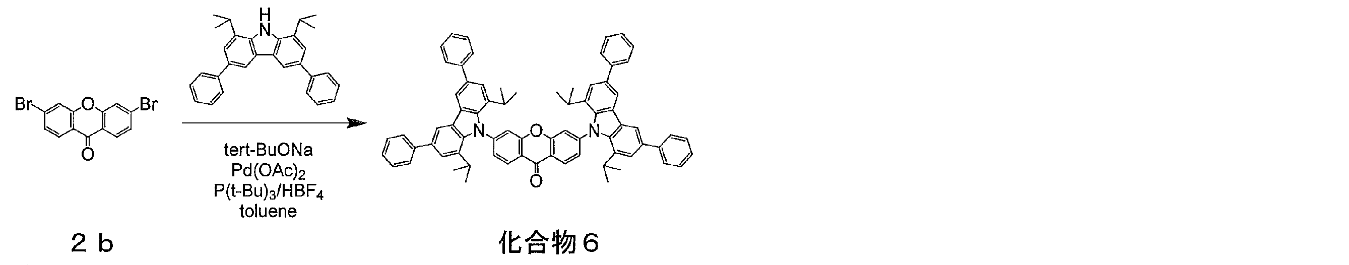
下記の反応式にしたがって、合成例1の化合物1と同様にして合成した(収率46%)。

ESI-MS(m/z)(M+):calcd 361.11 found 361.20
下記の反応式にしたがって、合成例1の化合物1と同様にして合成した(収率99%)。

ESI-MS(m/z)(M+):calcd 602.20 found 602.40
下記の反応式にしたがって、合成例2の化合物4と同様にして合成した(収率63%)。

下記の反応式にしたがって、合成例1の化合物1と同様にして合成した(収率92%)。

化合物1のトルエン溶液(濃度10-5mol/L)およびヘキサン溶液(濃度10-5mol/L)を調製した。
また、石英基板上に真空蒸着法にて、真空度10-4Pa以下の条件にて化合物1とmCBPとを異なる蒸着源から蒸着し、化合物1の濃度が6.0重量%である共蒸着薄膜を100nmの厚さで形成した。
化合物1のトルエン溶液とヘキサン溶液のそれぞれの過渡減衰曲線を図2に示す。このトルエン溶液の蛍光減衰時間は、τ1:48ns、τ2:1500nsであり、ヘキサン溶液の蛍光減衰時間は、τ1:18ns、τ2:385nsであった。
また、化合物1とmCBPの共蒸着薄膜について、325nm励起光による発光スペクトルを測定した結果を図3に示す。この共蒸着薄膜のフォトルミネッセンス量子効率は89%であった。
さらに、300K、200K、100K、5Kの各温度における共蒸着薄膜の過渡減衰曲線を図4に示す。図4より、温度上昇に伴って遅延蛍光成分が増加する熱活性型の遅延蛍光であることが確認された。
化合物1のかわりに化合物2を用いた点を変更して各サンプルを作製した。ただし、トルエン溶液およびヘキサン溶液は調製せず、共蒸着薄膜を作製するに際し、mCBPの代わりにmCPを使用した。
化合物2とmCPを有する共蒸着薄膜について、345nm励起光による発光スペクトルを測定した結果を図5に示す。この共蒸着薄膜のフォトルミネッセンス量子効率は66%であった。
また、300K、200K、100K、4Kの各温度における共蒸着薄膜の過渡減衰曲線を図6に示す。図6より、温度上昇に伴って遅延蛍光成分が増加する熱活性型の遅延蛍光であることが確認された。
化合物1のかわりに化合物3を用いた点を変更して各サンプルを作製した。ただし、共蒸着薄膜を作製するに際し、mCBPの代わりにmCPを使用した。
化合物3のトルエン溶液について、370nm励起光による発光スペクトルを測定した結果を図7に示す。フォトルミネッセンス量子効率は、窒素バブリングしたトルエン溶液で35%であった。
化合物3のトルエン溶液の過渡減衰曲線を図8に示す。このトルエン溶液の蛍光減衰時間は、τ1:3.2ns、τ2:11μsであり、遅延蛍光が確認された。
化合物3とmCPを有する共蒸着薄膜について、300nm励起光による発光スペクトルを測定した結果を図9に示す。この共蒸着薄膜のフォトルミネッセンス量子効率は30%であった。
さらに、300K、200K、4Kの各温度における共蒸着薄膜の過渡減衰曲線を図10に示す。図10より、温度上昇に伴って遅延蛍光成分が増加する熱活性型の遅延蛍光であることが確認された。
化合物1のかわりに化合物4を用いた点を変更して各サンプルを作製した。ただし、共蒸着薄膜を作製するに際し、mCBPの代わりにmCPを使用した。
化合物4のトルエン溶液およびヘキサン溶液の過渡減衰曲を図12に示す。このトルエン溶液の蛍光減衰時間は、τ1:47ns、τ2:1.7μsであり、ヘキサン溶液の蛍光減衰時間は、τ1:15ns、τ2:2.5μsであった。
化合物4とmCPを有する共蒸着薄膜について、325nm励起光による発光スペクトルを測定した結果を図11に示す。この共蒸着薄膜のフォトルミネッセンス量子効率は89%であった。
さらに、300K、200K、100K、4Kの各温度における共蒸着薄膜の過渡減衰曲線を図13に示す。図13より、温度上昇に伴って遅延蛍光成分が増加する熱活性型の遅延蛍光であることが確認された。
化合物1のかわりに化合物5を用いた点を変更してトルエン溶液を調製した。
化合物5のトルエン溶液について、380nm励起光による発光スペクトルを測定した結果を図14に示す。フォトルミネッセンス量子効率は、窒素バブリングなしのトルエン溶液で0.6%、窒素バブリングしたトルエン溶液で25%であった。
化合物5のトルエン溶液の過渡減衰曲線を図15に示す。このトルエン溶液の蛍光減衰時間は、516nmの蛍光でτ1:3.9ns、τ2:419ns、580nmの蛍光でτ1:4.1ns、τ2:415nsであり、遅延蛍光が確認された。
化合物1のかわりに化合物3を用いた点を変更してトルエン溶液を調整した。
化合物6のトルエン溶液について、370nm励起光による発光スペクトルを測定した結果を図16に示す。フォトルミネッセンス量子効率は、窒素バブリングしたトルエン溶液で32%であった。
化合物6のトルエン溶液の過渡減衰曲線を図17に示す。このトルエン溶液の蛍光減衰時間は、τ1:2.2ns、τ2:2.4μsであり、遅延蛍光が確認された。
化合物6とmCPを有する共蒸着薄膜について、370nm励起光による発光スペクトルを測定した結果を図18に示す。この共蒸着薄膜のフォトルミネッセンス量子効率は60%であった。
さらに、300K、200K、100K、4Kの各温度における共蒸着薄膜の過渡減衰曲線を図19に示す。図19より、温度上昇に伴って遅延蛍光成分が増加する熱活性型の遅延蛍光であることが確認された。
化合物1のかわりに化合物9を用いた点を変更してトルエン溶液を調製した。
化合物9のトルエン溶液について375nm励起光による発光スペクトルを測定した結果を図20に、フォトルミネッセンス量子効率を波長毎にプロットした結果を図21に示す。図21に示すように、フォトルミネッセンス量子効率は、窒素バブリングしたトルエン溶液よりも窒素バブリングなしのトルエン溶液の方が低い値になっている。これは、化合物9は遅延蛍光を示す蛍光物質であり、窒素バブリングなしの化合物9のトルエン溶液では、酸素により、励起三重項状態の励起子の励起一重項への逆項間交差が阻害されたからと推測される。
化合物1のかわりに化合物10を用いた点を変更してトルエン溶液を調整した。
化合物10のトルエン溶液について、420nm励起光による発光スペクトルを測定した結果を図22に示す。フォトルミネッセンス量子効率は、窒素バブリングしたトルエン溶液で44%であった。
化合物10のトルエン溶液の過渡減衰曲線を図23に示す。このトルエン溶液の蛍光減衰時間は、τ1:32ns、τ2:1.1μsであり、遅延蛍光が確認された。
化合物1のかわりに化合物11を用いた点を変更してトルエン溶液を調整した。
化合物11のトルエン溶液について、400nm励起光による発光スペクトルを測定した結果を図24に示す。フォトルミネッセンス量子効率は、窒素バブリングしたトルエン溶液で97%であった。
化合物11のトルエン溶液の過渡減衰曲線を図25に示す。このトルエン溶液の蛍光減衰時間は、τ1:37ns、τ2:3.8μsであり、遅延蛍光が確認された。
膜厚100nmのインジウム・スズ酸化物(ITO)からなる陽極が形成されたガラス基板上に、各薄膜を真空蒸着法にて、真空度5.0×10⁻⁴Paで積層した。まず、ITO上にα-NPDを40nmの厚さに形成した。次に、化合物1とmCPを異なる蒸着源から共蒸着し、20nmの厚さの層を形成して発光層とした。この時、化合物1の濃度は6.0重量%とした。次に、TPBiを40nmの厚さに形成し、さらにフッ化リチウム(LiF)を0.8nm真空蒸着し、次いでアルミニウム(Al)を80nmの厚さに蒸着することにより陰極を形成し、有機エレクトロルミネッセンス素子とした。
化合物1のかわりに化合物4を用いて同様にして有機エレクトロルミネッセンス素子を作製した。
化合物1を用いて作製した有機エレクトロルミネッセンス素子の発光スペクトルを図26に示し、化合物4を用いて作製した有機エレクトロルミネッセンス素子の発光スペクトルを図27に示す。また、作製した2種類の有機エレクトロルミネッセンス素子の電圧-電流密度特性を図28に示し、発光強度-外部量子効率特性を図29に示し、電流密度-外部量子効率特性を示すグラフを図30に示す。いずれの有機エレクトロルミネッセンス素子も、遅延蛍光を示さない通常の蛍光材料を発光材料として用いた場合の外部量子効率を上回る高い外部量子効率を達成した。特に化合物1を用いた有機エレクトロルミネッセンス素子は極めて高い外部量子効率を達成した。
また、mCPのかわりにCzDBFを使用し、TPBiのかわりにPPTを用いた場合も、同様に高い外部量子効率を達成した。
膜厚100nmのインジウム・スズ酸化物(ITO)からなる陽極が形成されたガラス基板上に、各薄膜を真空蒸着法にて、真空度5.0×10⁻⁴Paで積層した。まず、ITO上にHAT-CNを10nmの厚さに形成し、その上に、Tris-PCzを30nmの厚さに形成した。次に、化合物1とmCBPを異なる蒸着源から共蒸着し、30nmの厚さの層を形成して発光層とした。この時、化合物1の濃度は10重量%または20重量%とした。または、共蒸着を行う代わりに、化合物1のみを蒸着源として30nmの厚さに形成し、化合物1の濃度が100重量%の発光層とした。次に、T2Tを10nmの厚さに形成し、その上に、Bpy-TP2を40nmの厚さに形成した。さらにフッ化リチウム(LiF)を0.8nm真空蒸着し、次いでアルミニウム(Al)を100nmの厚さに蒸着することにより陰極を形成した。以上の工程により、発光層における化合物1の濃度が異なる3種類の有機エレクトロルミネッセンス素子を作製した。
化合物1の濃度を10重量%とした有機エレクトロルミネッセンス素子について、発光スペクトルを図31に示し、電圧-電流密度特性を図32に示し、発光強度-外部量子効率特性を図33に示し、電流密度-外部量子効率特性を図34に示す。化合物1の濃度を20重量%とした有機エレクトロルミネッセンス素子について、発光スペクトルを図35に示し、電圧-電流密度特性を図36に示し、発光強度-外部量子効率特性を図37に示し、電流密度-外部量子効率特性を図38に示す。化合物1の濃度を100重量%とした有機エレクトロルミネッセンス素子について、発光スペクトルを図39に示し、電圧-電流密度特性を図40に示し、発光強度-外部量子効率特性を図41に示し、電流密度-外部量子効率特性を図42に示す。また、各有機エレクトロルミネッセンス素子のデバイス特性を表1にまとめて示す。いずれの有機エレクトロルミネッセンス素子も、遅延蛍光を示さない通常の蛍光材料を発光材料として用いた場合の外部量子効率を上回る高い外部量子効率を達成した。
膜厚100nmのインジウム・スズ酸化物(ITO)からなる陽極が形成されたガラス基板上に、各薄膜を真空蒸着法にて、真空度5.0×10⁻⁴Paで積層した。まず、ITO上にHAT-CNを10nmの厚さに形成した。次に、Tris-PCzを20nmの厚さに形成し、その上に、CCPを10nmの厚さに形成した。次に、化合物4とCO(mQPh)2を異なる蒸着源から共蒸着し、30nmの厚さの層を形成して発光層とした。この時、化合物4の濃度は20重量%とした。次に、CO(mQPh)2を10nmの厚さに形成し、その上に、Bpy-TP2を20nmの厚さに形成した。さらにフッ化リチウム(LiF)を0.8nm真空蒸着し、次いでアルミニウム(Al)を100nmの厚さに蒸着することにより陰極を形成し、有機エレクトロルミネッセンス素子とした。
作製した有機エレクトロルミネッセンス素子の発光スペクトルを図43に示し、電圧-電流密度特性を図44に示し、発光強度-外部量子効率特性を図45に示し、電流密度-外部量子効率特性を図46に示す。また、作製した有機エレクトロルミネッセンス素子のデバイス特性を表1に示す。この有機エレクトロルミネッセンス素子は、遅延蛍光を示さない通常の蛍光材料を発光材料として用いた場合の外部量子効率を上回る高い外部量子効率を達成した。
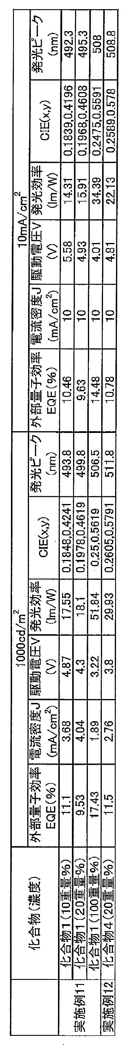


2 陽極
3 正孔注入層
4 正孔輸送層
5 発光層
6 電子輸送層
7 陰極
Claims (15)
- 下記一般式(1)で表される化合物からなる発光材料。
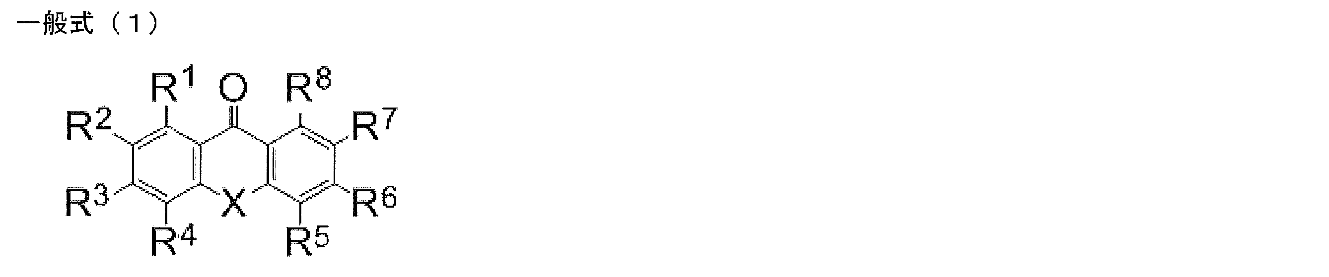
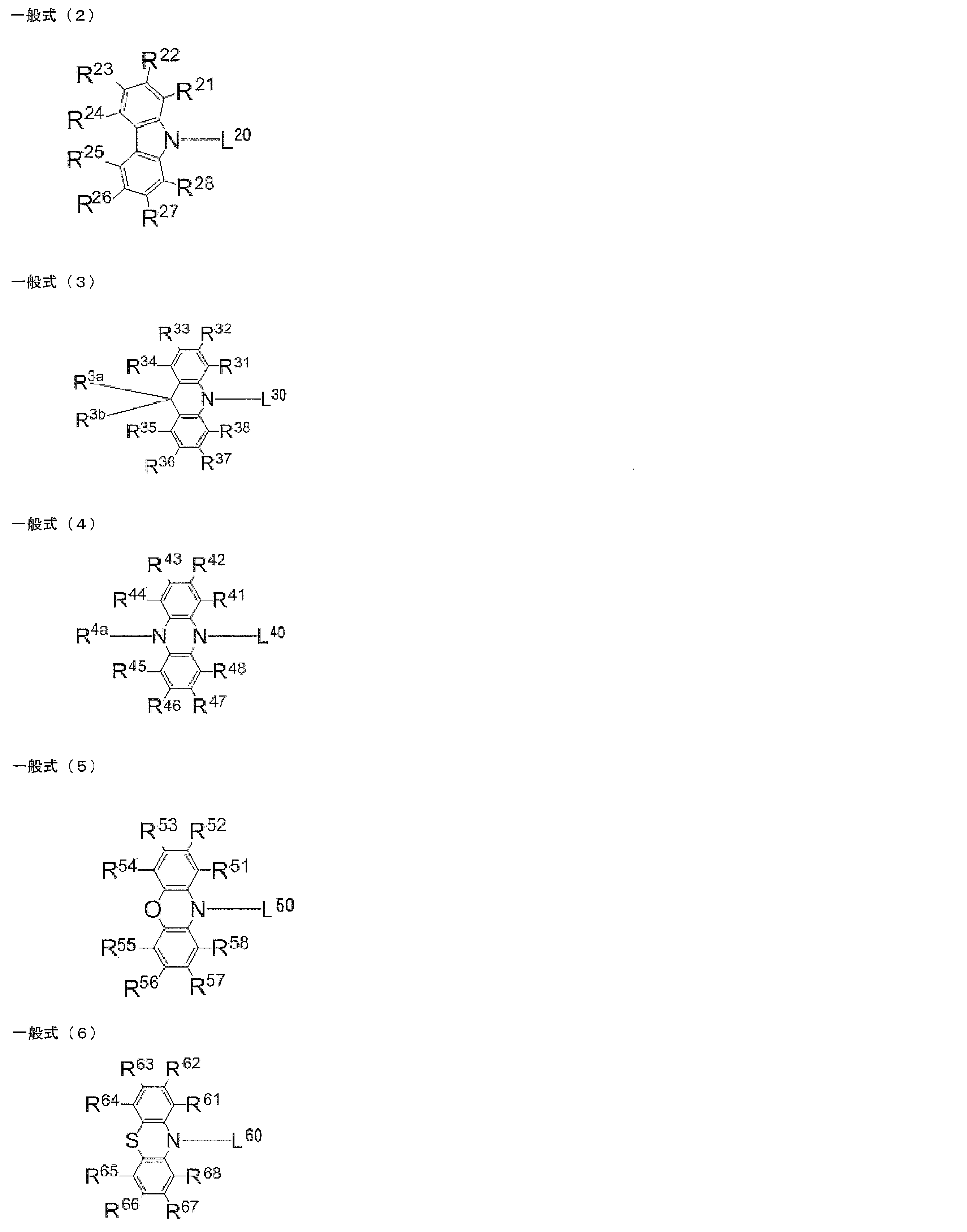
- 前記一般式(1)のR3またはR6のうちの少なくとも1つが、前記一般式(2)~(6)のいずれかで表される基であることを特徴とする請求項1に記載の発光材料。
- 前記一般式(1)のR3とR6が、前記一般式(2)~(6)のいずれかで表される基であることを特徴とする請求項2に記載の発光材料。
- 前記一般式(1)のR3またはR6のうちの少なくとも1つが、前記一般式(3)で表される基であることを特徴とする請求項2に記載の発光材料。
- 前記一般式(1)のR3またはR6のうちの少なくとも1つが、前記一般式(2)で表される基であることを特徴とする請求項2に記載の発光材料。
- 前記一般式(2)~(6)のR21~R28、R31~R38、R41~R48、R51~R58、R61~R68の少なくとも1つが、置換基であることを特徴とする請求項1~5のいずれか1項に記載の発光材料。
- 前記一般式(2)~(6)のR23、R26、R33、R36、R43、R46、R53、R56、R63、R66の少なくとも1つが、置換基であることを特徴とする請求項6に記載の発光材料。
- 前記置換基が、前記一般式(2)~(6)のいずれかで表される基であることを特徴とする請求項7に記載の発光材料。
- 前記一般式(2)~(6)のLが、単結合であることを特徴とする請求項1~8のいずれか1項に記載の発光材料。
- 前記一般式(1)のXが、酸素原子であることを特徴とする請求項1~9のいずれか1項に記載の発光材料。
- 下記一般式(1)で表される化合物からなる遅延蛍光体。

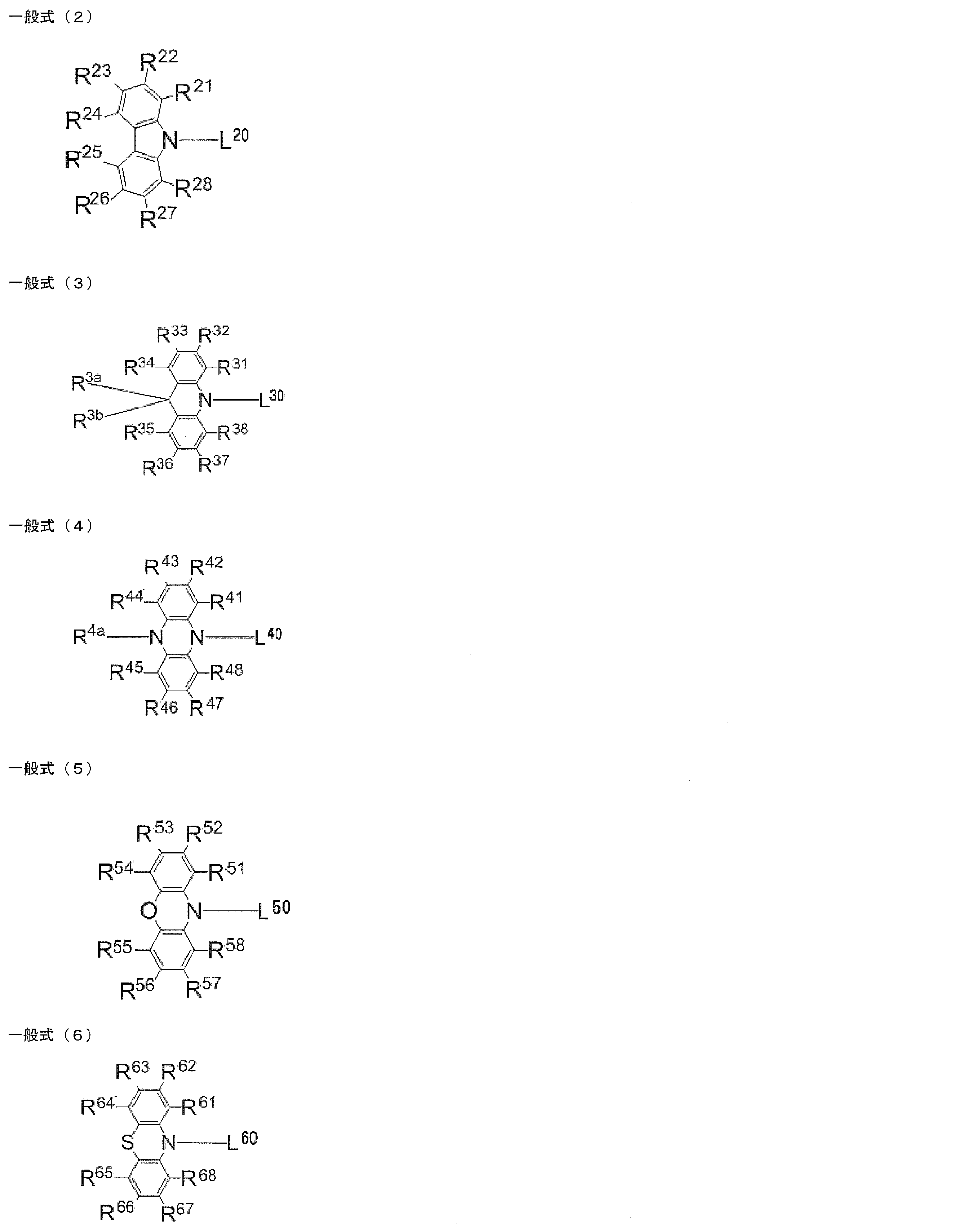
- 請求項1~10のいずれか1項に記載の発光材料を含むことを特徴とする有機発光素子。
- 遅延蛍光を放射することを特徴とする請求項12に記載の有機発光素子。
- 有機エレクトロルミネッセンス素子であることを特徴とする請求項12または13に記載の有機発光素子。
- 下記一般式(1’)で表される化合物。

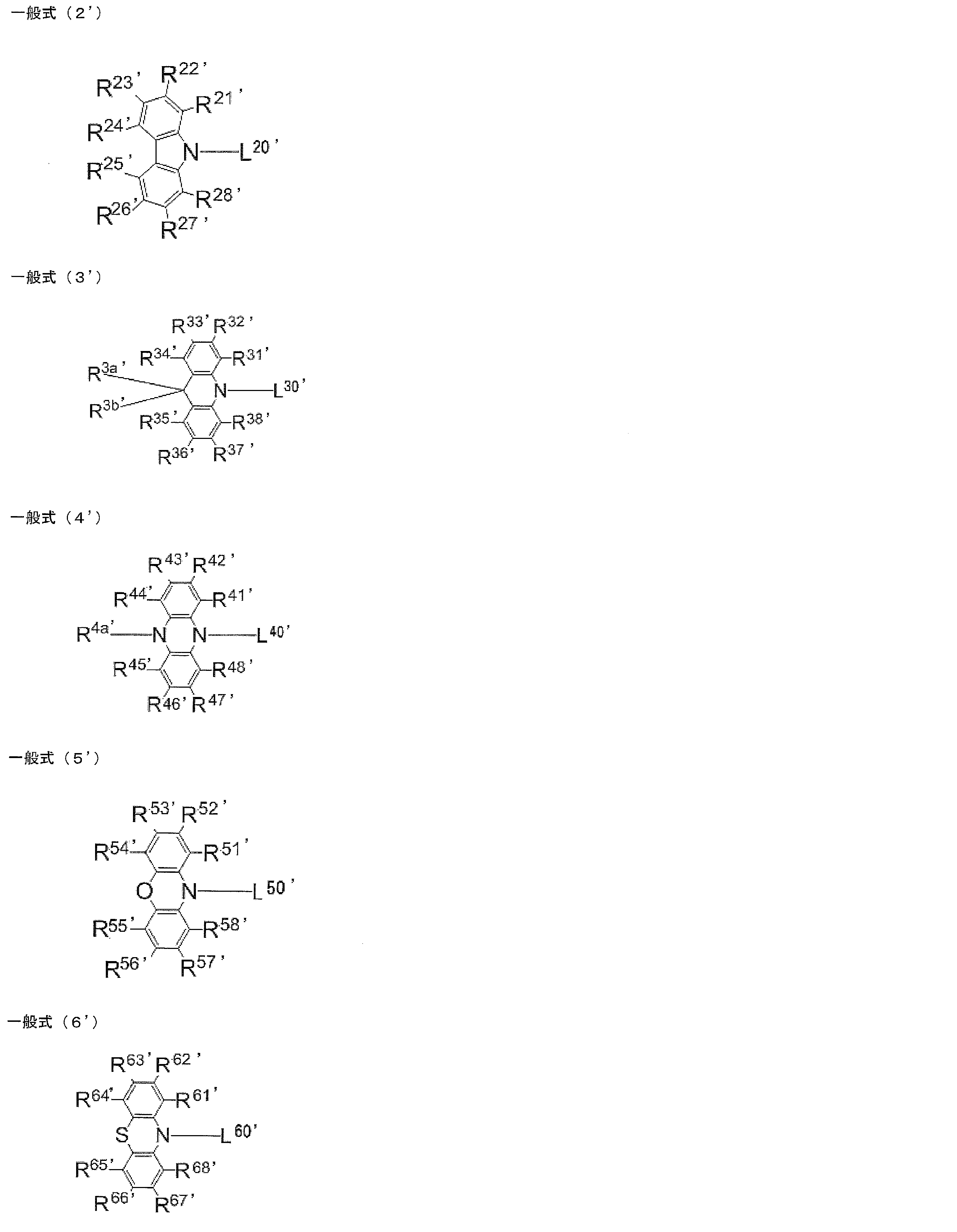
Priority Applications (3)
| Application Number | Priority Date | Filing Date | Title |
|---|---|---|---|
| US14/901,533 US9685615B2 (en) | 2013-07-03 | 2014-07-02 | Light emitting material, delayed fluorescent emitter, organic light emitting device, and compound |
| CN201480035796.2A CN105340101B (zh) | 2013-07-03 | 2014-07-02 | 发光材料、延迟萤光体、有机发光元件及化合物 |
| JP2015525248A JP6521253B2 (ja) | 2013-07-03 | 2014-07-02 | 発光材料、遅延蛍光体、有機発光素子および化合物 |
Applications Claiming Priority (2)
| Application Number | Priority Date | Filing Date | Title |
|---|---|---|---|
| JP2013-139975 | 2013-07-03 | ||
| JP2013139975 | 2013-07-03 |
Publications (1)
| Publication Number | Publication Date |
|---|---|
| WO2015002213A1 true WO2015002213A1 (ja) | 2015-01-08 |
Family
ID=52143785
Family Applications (1)
| Application Number | Title | Priority Date | Filing Date |
|---|---|---|---|
| PCT/JP2014/067611 WO2015002213A1 (ja) | 2013-07-03 | 2014-07-02 | 発光材料、遅延蛍光体、有機発光素子および化合物 |
Country Status (5)
| Country | Link |
|---|---|
| US (1) | US9685615B2 (ja) |
| JP (1) | JP6521253B2 (ja) |
| CN (1) | CN105340101B (ja) |
| TW (1) | TW201508001A (ja) |
| WO (1) | WO2015002213A1 (ja) |
Cited By (24)
| Publication number | Priority date | Publication date | Assignee | Title |
|---|---|---|---|---|
| JP2015053476A (ja) * | 2013-07-30 | 2015-03-19 | 出光興産株式会社 | 有機エレクトロルミネッセンス素子および電子機器 |
| WO2016010136A1 (ja) * | 2014-07-18 | 2016-01-21 | 国立大学法人九州大学 | 有機発光素子 |
| WO2016027760A1 (ja) * | 2014-08-22 | 2016-02-25 | シャープ株式会社 | 有機エレクトロルミネッセンス素子およびその製造方法並びに発光方法 |
| CN107245079A (zh) * | 2016-12-30 | 2017-10-13 | 江苏三月光电科技有限公司 | 一种氮杂氧杂蒽酮类化合物及其在oled器件上的应用 |
| US20170352817A1 (en) * | 2016-06-02 | 2017-12-07 | Samsung Display Co., Ltd. | Polycyclic compound and organic electroluminescence device including the same |
| WO2018014406A1 (zh) * | 2016-07-20 | 2018-01-25 | 深圳市华星光电技术有限公司 | 发光材料及其制备方法与使用该发光材料的有机发光二极管 |
| WO2020076796A1 (en) | 2018-10-09 | 2020-04-16 | Kyulux, Inc. | Novel composition of matter for use in organic light-emitting diodes |
| WO2021157593A1 (ja) | 2020-02-04 | 2021-08-12 | 株式会社Kyulux | 組成物、膜、有機発光素子、発光組成物を提供する方法およびプログラム |
| US11101440B2 (en) | 2015-07-01 | 2021-08-24 | Kyushu University, National University Corporation | Organic electroluminescent device |
| WO2021235549A1 (ja) | 2020-05-22 | 2021-11-25 | 株式会社Kyulux | 化合物、発光材料および発光素子 |
| WO2022025248A1 (ja) | 2020-07-31 | 2022-02-03 | 株式会社Kyulux | 化合物、発光材料および発光素子 |
| US11335872B2 (en) | 2016-09-06 | 2022-05-17 | Kyulux, Inc. | Organic light-emitting device |
| WO2022168956A1 (ja) | 2021-02-04 | 2022-08-11 | 株式会社Kyulux | 化合物、発光材料および有機発光素子 |
| US11476435B2 (en) | 2017-08-24 | 2022-10-18 | Kyushu University, National University Corporation | Film and organic light-emitting device containing perovskite-type compound and organic light-emitting material |
| US11482679B2 (en) | 2017-05-23 | 2022-10-25 | Kyushu University, National University Corporation | Compound, light-emitting lifetime lengthening agent, use of n-type compound, film and light-emitting device |
| WO2022244503A1 (ja) | 2021-05-20 | 2022-11-24 | 株式会社Kyulux | 有機発光素子 |
| WO2022270354A1 (ja) | 2021-06-23 | 2022-12-29 | 株式会社Kyulux | 化合物、発光材料および有機発光素子 |
| WO2022270602A1 (ja) | 2021-06-23 | 2022-12-29 | 株式会社Kyulux | 有機発光素子および膜 |
| WO2022270113A1 (ja) | 2021-06-23 | 2022-12-29 | 株式会社Kyulux | 有機エレクトロルミネッセンス素子 |
| WO2023282224A1 (ja) | 2021-07-06 | 2023-01-12 | 株式会社Kyulux | 有機発光素子およびその設計方法 |
| WO2023053835A1 (ja) | 2021-09-28 | 2023-04-06 | 株式会社Kyulux | 化合物、組成物、ホスト材料、電子障壁材料および有機発光素子 |
| US11930654B2 (en) | 2017-07-06 | 2024-03-12 | Kyulux, Inc. | Organic light-emitting element |
| US11957043B2 (en) | 2020-05-06 | 2024-04-09 | Samsung Display Co., Ltd. | Light-emitting device and electronic apparatus comprising same |
| KR102660767B1 (ko) * | 2015-02-06 | 2024-04-24 | 이데미쓰 고산 가부시키가이샤 | 유기 일렉트로루미네센스 소자 및 전자 기기 |
Families Citing this family (38)
| Publication number | Priority date | Publication date | Assignee | Title |
|---|---|---|---|---|
| CN107056758B (zh) * | 2016-04-25 | 2020-06-09 | 中节能万润股份有限公司 | 一种以吖啶螺蒽酮为核心的化合物及其在有机电致发光器件上的应用 |
| CN106220645B (zh) * | 2016-04-25 | 2018-08-14 | 中节能万润股份有限公司 | 一种基于单取代基-9-芴酮的化合物及其应用 |
| CN107068910B (zh) * | 2016-04-25 | 2019-07-19 | 中节能万润股份有限公司 | 一种含氧杂蒽酮类化合物的有机电致发光器件及其应用 |
| CN106220638B (zh) * | 2016-04-25 | 2018-06-26 | 中节能万润股份有限公司 | 一种基于氧杂蒽酮的化合物及其应用 |
| CN107093676B (zh) * | 2016-04-25 | 2019-06-14 | 中节能万润股份有限公司 | 一种含有吖啶螺蒽酮类化合物的有机电致发光器件及其应用 |
| CN107057680A (zh) * | 2016-04-25 | 2017-08-18 | 中节能万润股份有限公司 | 一种以蒽酮为核心的化合物及其在有机电致发光器件上的应用 |
| CN106279130A (zh) * | 2016-07-20 | 2017-01-04 | 深圳市华星光电技术有限公司 | 发光材料及其制备方法与使用该发光材料的有机发光二极管 |
| CN106317008A (zh) * | 2016-07-20 | 2017-01-11 | 深圳市华星光电技术有限公司 | 发光材料及其制备方法与使用该发光材料的有机发光二极管 |
| CN106317041A (zh) * | 2016-07-20 | 2017-01-11 | 深圳市华星光电技术有限公司 | 发光材料及其制备方法与使用该发光材料的有机发光二极管 |
| CN106167487A (zh) * | 2016-07-20 | 2016-11-30 | 深圳市华星光电技术有限公司 | 发光材料及其制备方法与使用该发光材料的有机发光二极管 |
| CN106467523B (zh) * | 2016-07-29 | 2019-04-09 | 江苏三月光电科技有限公司 | 一种有机芳香化合物及其应用 |
| CN106467524B (zh) * | 2016-07-29 | 2019-04-19 | 江苏三月光电科技有限公司 | 一种有机芳香化合物及其在有机电致发光器件上的应用 |
| CN106467497B (zh) * | 2016-08-18 | 2020-07-21 | 中节能万润股份有限公司 | 一种以蒽酮为核心的化合物及其在oled器件中的应用 |
| CN106467542B (zh) * | 2016-08-18 | 2019-06-14 | 江苏三月光电科技有限公司 | 一种以蒽酮为核心的化合物及其应用 |
| CN106467550B (zh) * | 2016-08-18 | 2020-03-27 | 江苏三月光电科技有限公司 | 一种以氧杂蒽酮为核心的二苯并六元环取代化合物及其应用 |
| CN106478611B (zh) * | 2016-08-26 | 2019-05-24 | 江苏三月光电科技有限公司 | 一种以氧杂蒽为核心的有机化合物及其应用 |
| CN106800557B (zh) * | 2016-12-05 | 2018-12-18 | 中节能万润股份有限公司 | 一种二氧吩恶噻类衍生物及其制备方法和应用 |
| CN106749290B (zh) * | 2016-12-09 | 2019-02-26 | 中节能万润股份有限公司 | 一种基于氧化硫杂蒽酮的化合物、制备方法及其应用 |
| CN106749200A (zh) * | 2016-12-14 | 2017-05-31 | 中节能万润股份有限公司 | 一种苯并吡喃‑4‑酮类有机电致发光材料及其制备方法和应用 |
| CN108250129B (zh) * | 2016-12-29 | 2021-11-30 | 中节能万润股份有限公司 | 一种以二芳基蒽酮为核心的化合物及其在有机电致发光器件上的应用 |
| CN106800558B (zh) * | 2016-12-29 | 2019-09-17 | 中节能万润股份有限公司 | 一种二氧化噻吨类有机电致发光材料及其制备方法和应用 |
| CN106800559B (zh) * | 2016-12-29 | 2019-04-30 | 中节能万润股份有限公司 | 一种噻吨类有机电致发光材料及其制备方法和应用 |
| CN108269924B (zh) * | 2016-12-30 | 2019-12-03 | 昆山国显光电有限公司 | 一种有机发光二极管 |
| CN106831744A (zh) * | 2016-12-30 | 2017-06-13 | 上海天马有机发光显示技术有限公司 | 一种有机电致发光材料以及有机光电装置 |
| CN108346756B (zh) * | 2017-01-24 | 2020-03-20 | 中节能万润股份有限公司 | 一种有机电致发光器件 |
| KR20200142554A (ko) | 2018-04-11 | 2020-12-22 | 나노코 테크놀로지스 리미티드 | 형광 공여체 지원 oled 장치를 위한 양자점 아키텍처 |
| EP3762470B1 (en) | 2018-04-11 | 2023-11-29 | Kyulux, Inc. | Top-emitting printed display with quantum dots and thermally activated delayed fluorescence molecules |
| CN110372691B (zh) * | 2018-04-13 | 2021-10-22 | 江苏三月科技股份有限公司 | 一种以氧杂蒽酮为核心的化合物、其制备方法及其在oled上的应用 |
| CN110526905B (zh) * | 2018-05-25 | 2020-11-20 | 江苏三月科技股份有限公司 | 一种含酮的化合物及其在有机电致发光器件上的应用 |
| CN110551112A (zh) * | 2018-05-31 | 2019-12-10 | 江苏三月光电科技有限公司 | 一种含二氰基吡嗪的化合物及其在有机电致发光器件上的应用 |
| CN110551132A (zh) * | 2018-05-31 | 2019-12-10 | 江苏三月光电科技有限公司 | 一种含酮的化合物及其在有机电致发光器件上的应用 |
| CN108997299B (zh) * | 2018-07-09 | 2020-04-03 | 北京师范大学 | 一种高效长寿命的有机室温磷光材料及其制备方法 |
| WO2020099826A1 (en) | 2018-11-16 | 2020-05-22 | Nanoco Technologies Ltd | Electroluminescent display devices and methods of making the same |
| CN111200067B (zh) * | 2018-11-20 | 2022-08-02 | 江苏三月科技股份有限公司 | 有机电致发光器件、其制备方法及包含其的显示装置 |
| KR102505882B1 (ko) | 2019-10-04 | 2023-03-06 | 삼성디스플레이 주식회사 | 유기 발광 소자 및 이를 포함하는 장치 |
| KR102544979B1 (ko) | 2019-10-04 | 2023-06-20 | 삼성디스플레이 주식회사 | 유기 발광 소자 및 이를 포함하는 장치 |
| CN114249713B (zh) * | 2020-09-22 | 2024-05-03 | 江苏三月科技股份有限公司 | 一种含有氧杂蒽酮或硫杂蒽酮结构的有机化合物及其应用 |
| CN112142725A (zh) * | 2020-09-29 | 2020-12-29 | 华南理工大学 | 一类基于占吨酮的有机电致发光材料及其在制备oled中的应用 |
Citations (6)
| Publication number | Priority date | Publication date | Assignee | Title |
|---|---|---|---|---|
| WO2006114966A1 (ja) * | 2005-04-18 | 2006-11-02 | Konica Minolta Holdings, Inc. | 有機エレクトロルミネッセンス素子、表示装置及び照明装置 |
| JP2011249754A (ja) * | 2010-04-26 | 2011-12-08 | Canon Inc | 有機発光素子 |
| JP2012097051A (ja) * | 2010-11-04 | 2012-05-24 | Canon Inc | キサントン化合物およびそれを有する有機発光素子 |
| JP2012102024A (ja) * | 2010-11-08 | 2012-05-31 | Canon Inc | チオキサントン化合物及びこれを有する有機発光素子 |
| JP2013016728A (ja) * | 2011-07-06 | 2013-01-24 | Canon Inc | 有機発光素子、発光装置、画像形成装置、表示装置および撮像装置 |
| WO2014067614A1 (de) * | 2012-10-31 | 2014-05-08 | Merck Patent Gmbh | Elektronische vorrichtung |
Family Cites Families (3)
| Publication number | Priority date | Publication date | Assignee | Title |
|---|---|---|---|---|
| JP2008037930A (ja) * | 2006-08-02 | 2008-02-21 | Toyo Ink Mfg Co Ltd | 光硬化型インクジェットインキ |
| US9090819B2 (en) | 2009-06-24 | 2015-07-28 | Konica Minolta, Inc. | Organic electroluminescent element, display device, illuminating device and condensed polycyclic heterocyclic compound |
| US9124461B2 (en) | 2011-07-18 | 2015-09-01 | Marvell Israel (M.I.S.L) Ltd. | Method and apparatus for reducing jitter |
-
2014
- 2014-07-02 US US14/901,533 patent/US9685615B2/en active Active
- 2014-07-02 CN CN201480035796.2A patent/CN105340101B/zh active Active
- 2014-07-02 JP JP2015525248A patent/JP6521253B2/ja active Active
- 2014-07-02 WO PCT/JP2014/067611 patent/WO2015002213A1/ja active Application Filing
- 2014-07-03 TW TW103123057A patent/TW201508001A/zh unknown
Patent Citations (6)
| Publication number | Priority date | Publication date | Assignee | Title |
|---|---|---|---|---|
| WO2006114966A1 (ja) * | 2005-04-18 | 2006-11-02 | Konica Minolta Holdings, Inc. | 有機エレクトロルミネッセンス素子、表示装置及び照明装置 |
| JP2011249754A (ja) * | 2010-04-26 | 2011-12-08 | Canon Inc | 有機発光素子 |
| JP2012097051A (ja) * | 2010-11-04 | 2012-05-24 | Canon Inc | キサントン化合物およびそれを有する有機発光素子 |
| JP2012102024A (ja) * | 2010-11-08 | 2012-05-31 | Canon Inc | チオキサントン化合物及びこれを有する有機発光素子 |
| JP2013016728A (ja) * | 2011-07-06 | 2013-01-24 | Canon Inc | 有機発光素子、発光装置、画像形成装置、表示装置および撮像装置 |
| WO2014067614A1 (de) * | 2012-10-31 | 2014-05-08 | Merck Patent Gmbh | Elektronische vorrichtung |
Non-Patent Citations (1)
| Title |
|---|
| Y.WANG ET AL.: "Synthesis of ''donor-bridge- acceptor'' triad compounds containing the aromatic sulfur bridges", DYES AND PIGMENTS, vol. 44, 2000, pages 93 - 100, XP004244385, DOI: doi:10.1016/S0143-7208(99)00076-5 * |
Cited By (30)
| Publication number | Priority date | Publication date | Assignee | Title |
|---|---|---|---|---|
| JP2015053476A (ja) * | 2013-07-30 | 2015-03-19 | 出光興産株式会社 | 有機エレクトロルミネッセンス素子および電子機器 |
| WO2016010136A1 (ja) * | 2014-07-18 | 2016-01-21 | 国立大学法人九州大学 | 有機発光素子 |
| WO2016027760A1 (ja) * | 2014-08-22 | 2016-02-25 | シャープ株式会社 | 有機エレクトロルミネッセンス素子およびその製造方法並びに発光方法 |
| JPWO2016027760A1 (ja) * | 2014-08-22 | 2017-04-27 | シャープ株式会社 | 有機エレクトロルミネッセンス素子およびその製造方法並びに発光方法 |
| US10276819B2 (en) | 2014-08-22 | 2019-04-30 | Sharp Kabushiki Kaisha | Organic electroluminescent element, manufacturing method for same, and light emission method including a thermally activated delayed fluorescent material |
| KR102660767B1 (ko) * | 2015-02-06 | 2024-04-24 | 이데미쓰 고산 가부시키가이샤 | 유기 일렉트로루미네센스 소자 및 전자 기기 |
| US11101440B2 (en) | 2015-07-01 | 2021-08-24 | Kyushu University, National University Corporation | Organic electroluminescent device |
| JP2017218442A (ja) * | 2016-06-02 | 2017-12-14 | 三星ディスプレイ株式會社Samsung Display Co.,Ltd. | 多環化合物及び多環化合物を含む有機電界発光素子 |
| US20170352817A1 (en) * | 2016-06-02 | 2017-12-07 | Samsung Display Co., Ltd. | Polycyclic compound and organic electroluminescence device including the same |
| KR20170137262A (ko) | 2016-06-02 | 2017-12-13 | 삼성디스플레이 주식회사 | 다환 화합물 및 이를 포함하는 유기 전계 발광 소자 |
| US10714693B2 (en) | 2016-06-02 | 2020-07-14 | Samsung Display Co., Ltd. | Polycyclic compound and organic electroluminescence device including the same |
| WO2018014406A1 (zh) * | 2016-07-20 | 2018-01-25 | 深圳市华星光电技术有限公司 | 发光材料及其制备方法与使用该发光材料的有机发光二极管 |
| US11335872B2 (en) | 2016-09-06 | 2022-05-17 | Kyulux, Inc. | Organic light-emitting device |
| CN107245079A (zh) * | 2016-12-30 | 2017-10-13 | 江苏三月光电科技有限公司 | 一种氮杂氧杂蒽酮类化合物及其在oled器件上的应用 |
| US11482679B2 (en) | 2017-05-23 | 2022-10-25 | Kyushu University, National University Corporation | Compound, light-emitting lifetime lengthening agent, use of n-type compound, film and light-emitting device |
| US11930654B2 (en) | 2017-07-06 | 2024-03-12 | Kyulux, Inc. | Organic light-emitting element |
| US11476435B2 (en) | 2017-08-24 | 2022-10-18 | Kyushu University, National University Corporation | Film and organic light-emitting device containing perovskite-type compound and organic light-emitting material |
| WO2020076796A1 (en) | 2018-10-09 | 2020-04-16 | Kyulux, Inc. | Novel composition of matter for use in organic light-emitting diodes |
| WO2021157593A1 (ja) | 2020-02-04 | 2021-08-12 | 株式会社Kyulux | 組成物、膜、有機発光素子、発光組成物を提供する方法およびプログラム |
| WO2021157642A1 (ja) | 2020-02-04 | 2021-08-12 | 株式会社Kyulux | ホスト材料、組成物および有機発光素子 |
| US11957043B2 (en) | 2020-05-06 | 2024-04-09 | Samsung Display Co., Ltd. | Light-emitting device and electronic apparatus comprising same |
| WO2021235549A1 (ja) | 2020-05-22 | 2021-11-25 | 株式会社Kyulux | 化合物、発光材料および発光素子 |
| WO2022025248A1 (ja) | 2020-07-31 | 2022-02-03 | 株式会社Kyulux | 化合物、発光材料および発光素子 |
| WO2022168956A1 (ja) | 2021-02-04 | 2022-08-11 | 株式会社Kyulux | 化合物、発光材料および有機発光素子 |
| WO2022244503A1 (ja) | 2021-05-20 | 2022-11-24 | 株式会社Kyulux | 有機発光素子 |
| WO2022270113A1 (ja) | 2021-06-23 | 2022-12-29 | 株式会社Kyulux | 有機エレクトロルミネッセンス素子 |
| WO2022270602A1 (ja) | 2021-06-23 | 2022-12-29 | 株式会社Kyulux | 有機発光素子および膜 |
| WO2022270354A1 (ja) | 2021-06-23 | 2022-12-29 | 株式会社Kyulux | 化合物、発光材料および有機発光素子 |
| WO2023282224A1 (ja) | 2021-07-06 | 2023-01-12 | 株式会社Kyulux | 有機発光素子およびその設計方法 |
| WO2023053835A1 (ja) | 2021-09-28 | 2023-04-06 | 株式会社Kyulux | 化合物、組成物、ホスト材料、電子障壁材料および有機発光素子 |
Also Published As
| Publication number | Publication date |
|---|---|
| JP6521253B2 (ja) | 2019-05-29 |
| US20160141516A1 (en) | 2016-05-19 |
| CN105340101B (zh) | 2017-03-15 |
| US9685615B2 (en) | 2017-06-20 |
| TW201508001A (zh) | 2015-03-01 |
| JPWO2015002213A1 (ja) | 2017-02-23 |
| CN105340101A (zh) | 2016-02-17 |
Similar Documents
| Publication | Publication Date | Title |
|---|---|---|
| JP6521253B2 (ja) | 発光材料、遅延蛍光体、有機発光素子および化合物 | |
| JP7222549B2 (ja) | 化合物、発光材料および発光素子 | |
| JP6430370B2 (ja) | 発光材料、有機発光素子および化合物 | |
| JP6668152B2 (ja) | 化合物、発光材料および有機発光素子 | |
| JP6318155B2 (ja) | 化合物、発光材料および有機発光素子 | |
| JP6392240B2 (ja) | 発光材料、有機発光素子および化合物 | |
| KR101999881B1 (ko) | 화합물, 발광 재료 및 유기 발광 소자 | |
| JP6293417B2 (ja) | 化合物、発光材料および有機発光素子 | |
| WO2020039708A1 (ja) | 有機エレクトロルミネッセンス素子 | |
| WO2015133501A1 (ja) | 発光材料、有機発光素子および化合物 | |
| JP5366106B1 (ja) | 有機発光素子ならびにそれに用いる発光材料および化合物 | |
| JP6466913B2 (ja) | 発光材料、有機発光素子および化合物 | |
| JP6383538B2 (ja) | 発光材料、有機発光素子および化合物 | |
| WO2015080183A1 (ja) | 発光材料、有機発光素子および化合物 | |
| WO2013154064A1 (ja) | 有機発光素子ならびにそれに用いる発光材料および化合物 | |
| WO2013161437A1 (ja) | 発光材料および有機発光素子 | |
| JPWO2018159662A1 (ja) | 化合物、発光材料および有機発光素子 | |
| JP2017119663A (ja) | 化合物、発光材料および有機発光素子 | |
| JP6647514B2 (ja) | 有機発光素子ならびにそれに用いる発光材料および化合物 | |
| JP6249150B2 (ja) | 発光材料およびそれを用いた有機発光素子 | |
| JP6622484B2 (ja) | 発光材料、有機発光素子および化合物 | |
| JP2018111751A (ja) | 発光材料、化合物および有機発光素子 | |
| JP2016084283A (ja) | 化合物、発光材料および有機発光素子 |
Legal Events
| Date | Code | Title | Description |
|---|---|---|---|
| WWE | Wipo information: entry into national phase |
Ref document number: 201480035796.2 Country of ref document: CN |
|
| 121 | Ep: the epo has been informed by wipo that ep was designated in this application |
Ref document number: 14820497 Country of ref document: EP Kind code of ref document: A1 |
|
| ENP | Entry into the national phase |
Ref document number: 2015525248 Country of ref document: JP Kind code of ref document: A |
|
| WWE | Wipo information: entry into national phase |
Ref document number: 14901533 Country of ref document: US |
|
| NENP | Non-entry into the national phase |
Ref country code: DE |
|
| 122 | Ep: pct application non-entry in european phase |
Ref document number: 14820497 Country of ref document: EP Kind code of ref document: A1 |