WO2014208495A1 - Led装置 - Google Patents
Led装置 Download PDFInfo
- Publication number
- WO2014208495A1 WO2014208495A1 PCT/JP2014/066540 JP2014066540W WO2014208495A1 WO 2014208495 A1 WO2014208495 A1 WO 2014208495A1 JP 2014066540 W JP2014066540 W JP 2014066540W WO 2014208495 A1 WO2014208495 A1 WO 2014208495A1
- Authority
- WO
- WIPO (PCT)
- Prior art keywords
- electrode
- led
- led device
- frame
- die
- Prior art date
Links
- 239000000758 substrate Substances 0.000 claims abstract description 70
- 230000002093 peripheral effect Effects 0.000 claims description 13
- 239000007788 liquid Substances 0.000 abstract description 8
- 239000000126 substance Substances 0.000 abstract description 4
- 238000011109 contamination Methods 0.000 abstract description 2
- 229910000679 solder Inorganic materials 0.000 description 18
- OAICVXFJPJFONN-UHFFFAOYSA-N Phosphorus Chemical compound [P] OAICVXFJPJFONN-UHFFFAOYSA-N 0.000 description 17
- 238000009713 electroplating Methods 0.000 description 7
- 239000004065 semiconductor Substances 0.000 description 7
- 239000000463 material Substances 0.000 description 4
- 229910052594 sapphire Inorganic materials 0.000 description 3
- 239000010980 sapphire Substances 0.000 description 3
- PNEYBMLMFCGWSK-UHFFFAOYSA-N aluminium oxide Inorganic materials [O-2].[O-2].[O-2].[Al+3].[Al+3] PNEYBMLMFCGWSK-UHFFFAOYSA-N 0.000 description 2
- 239000000919 ceramic Substances 0.000 description 2
- 238000000576 coating method Methods 0.000 description 2
- 239000003086 colorant Substances 0.000 description 2
- 239000010949 copper Substances 0.000 description 2
- 238000010586 diagram Methods 0.000 description 2
- 229910052751 metal Inorganic materials 0.000 description 2
- 239000002184 metal Substances 0.000 description 2
- 230000005012 migration Effects 0.000 description 2
- 238000013508 migration Methods 0.000 description 2
- 230000000149 penetrating effect Effects 0.000 description 2
- 229920001296 polysiloxane Polymers 0.000 description 2
- 239000011347 resin Substances 0.000 description 2
- 229920005989 resin Polymers 0.000 description 2
- RYGMFSIKBFXOCR-UHFFFAOYSA-N Copper Chemical compound [Cu] RYGMFSIKBFXOCR-UHFFFAOYSA-N 0.000 description 1
- GWEVSGVZZGPLCZ-UHFFFAOYSA-N Titan oxide Chemical compound O=[Ti]=O GWEVSGVZZGPLCZ-UHFFFAOYSA-N 0.000 description 1
- 239000003990 capacitor Substances 0.000 description 1
- 239000011248 coating agent Substances 0.000 description 1
- 229910052802 copper Inorganic materials 0.000 description 1
- PMHQVHHXPFUNSP-UHFFFAOYSA-M copper(1+);methylsulfanylmethane;bromide Chemical compound Br[Cu].CSC PMHQVHHXPFUNSP-UHFFFAOYSA-M 0.000 description 1
- 238000005520 cutting process Methods 0.000 description 1
- 229910052737 gold Inorganic materials 0.000 description 1
- 239000011810 insulating material Substances 0.000 description 1
- 238000005304 joining Methods 0.000 description 1
- 238000004519 manufacturing process Methods 0.000 description 1
- 229910052759 nickel Inorganic materials 0.000 description 1
- 230000001681 protective effect Effects 0.000 description 1
- 238000002310 reflectometry Methods 0.000 description 1
- 150000003839 salts Chemical class 0.000 description 1
- 238000005476 soldering Methods 0.000 description 1
- OGIDPMRJRNCKJF-UHFFFAOYSA-N titanium oxide Inorganic materials [Ti]=O OGIDPMRJRNCKJF-UHFFFAOYSA-N 0.000 description 1
Images


Classifications
-
- H—ELECTRICITY
- H01—ELECTRIC ELEMENTS
- H01L—SEMICONDUCTOR DEVICES NOT COVERED BY CLASS H10
- H01L33/00—Semiconductor devices having potential barriers specially adapted for light emission; Processes or apparatus specially adapted for the manufacture or treatment thereof or of parts thereof; Details thereof
- H01L33/48—Semiconductor devices having potential barriers specially adapted for light emission; Processes or apparatus specially adapted for the manufacture or treatment thereof or of parts thereof; Details thereof characterised by the semiconductor body packages
- H01L33/62—Arrangements for conducting electric current to or from the semiconductor body, e.g. lead-frames, wire-bonds or solder balls
-
- H—ELECTRICITY
- H01—ELECTRIC ELEMENTS
- H01L—SEMICONDUCTOR DEVICES NOT COVERED BY CLASS H10
- H01L27/00—Devices consisting of a plurality of semiconductor or other solid-state components formed in or on a common substrate
- H01L27/15—Devices consisting of a plurality of semiconductor or other solid-state components formed in or on a common substrate including semiconductor components having potential barriers, specially adapted for light emission
- H01L27/153—Devices consisting of a plurality of semiconductor or other solid-state components formed in or on a common substrate including semiconductor components having potential barriers, specially adapted for light emission in a repetitive configuration, e.g. LED bars
- H01L27/156—Devices consisting of a plurality of semiconductor or other solid-state components formed in or on a common substrate including semiconductor components having potential barriers, specially adapted for light emission in a repetitive configuration, e.g. LED bars two-dimensional arrays
-
- H—ELECTRICITY
- H01—ELECTRIC ELEMENTS
- H01L—SEMICONDUCTOR DEVICES NOT COVERED BY CLASS H10
- H01L33/00—Semiconductor devices having potential barriers specially adapted for light emission; Processes or apparatus specially adapted for the manufacture or treatment thereof or of parts thereof; Details thereof
- H01L33/36—Semiconductor devices having potential barriers specially adapted for light emission; Processes or apparatus specially adapted for the manufacture or treatment thereof or of parts thereof; Details thereof characterised by the electrodes
- H01L33/38—Semiconductor devices having potential barriers specially adapted for light emission; Processes or apparatus specially adapted for the manufacture or treatment thereof or of parts thereof; Details thereof characterised by the electrodes with a particular shape
- H01L33/387—Semiconductor devices having potential barriers specially adapted for light emission; Processes or apparatus specially adapted for the manufacture or treatment thereof or of parts thereof; Details thereof characterised by the electrodes with a particular shape with a plurality of electrode regions in direct contact with the semiconductor body and being electrically interconnected by another electrode layer
-
- H—ELECTRICITY
- H01—ELECTRIC ELEMENTS
- H01L—SEMICONDUCTOR DEVICES NOT COVERED BY CLASS H10
- H01L33/00—Semiconductor devices having potential barriers specially adapted for light emission; Processes or apparatus specially adapted for the manufacture or treatment thereof or of parts thereof; Details thereof
- H01L33/48—Semiconductor devices having potential barriers specially adapted for light emission; Processes or apparatus specially adapted for the manufacture or treatment thereof or of parts thereof; Details thereof characterised by the semiconductor body packages
- H01L33/483—Containers
- H01L33/486—Containers adapted for surface mounting
-
- H—ELECTRICITY
- H01—ELECTRIC ELEMENTS
- H01L—SEMICONDUCTOR DEVICES NOT COVERED BY CLASS H10
- H01L2224/00—Indexing scheme for arrangements for connecting or disconnecting semiconductor or solid-state bodies and methods related thereto as covered by H01L24/00
- H01L2224/01—Means for bonding being attached to, or being formed on, the surface to be connected, e.g. chip-to-package, die-attach, "first-level" interconnects; Manufacturing methods related thereto
- H01L2224/42—Wire connectors; Manufacturing methods related thereto
- H01L2224/47—Structure, shape, material or disposition of the wire connectors after the connecting process
- H01L2224/48—Structure, shape, material or disposition of the wire connectors after the connecting process of an individual wire connector
- H01L2224/4805—Shape
- H01L2224/4809—Loop shape
- H01L2224/48091—Arched
-
- H—ELECTRICITY
- H01—ELECTRIC ELEMENTS
- H01L—SEMICONDUCTOR DEVICES NOT COVERED BY CLASS H10
- H01L2224/00—Indexing scheme for arrangements for connecting or disconnecting semiconductor or solid-state bodies and methods related thereto as covered by H01L24/00
- H01L2224/01—Means for bonding being attached to, or being formed on, the surface to be connected, e.g. chip-to-package, die-attach, "first-level" interconnects; Manufacturing methods related thereto
- H01L2224/42—Wire connectors; Manufacturing methods related thereto
- H01L2224/47—Structure, shape, material or disposition of the wire connectors after the connecting process
- H01L2224/48—Structure, shape, material or disposition of the wire connectors after the connecting process of an individual wire connector
- H01L2224/481—Disposition
- H01L2224/48151—Connecting between a semiconductor or solid-state body and an item not being a semiconductor or solid-state body, e.g. chip-to-substrate, chip-to-passive
- H01L2224/48221—Connecting between a semiconductor or solid-state body and an item not being a semiconductor or solid-state body, e.g. chip-to-substrate, chip-to-passive the body and the item being stacked
- H01L2224/48225—Connecting between a semiconductor or solid-state body and an item not being a semiconductor or solid-state body, e.g. chip-to-substrate, chip-to-passive the body and the item being stacked the item being non-metallic, e.g. insulating substrate with or without metallisation
- H01L2224/48227—Connecting between a semiconductor or solid-state body and an item not being a semiconductor or solid-state body, e.g. chip-to-substrate, chip-to-passive the body and the item being stacked the item being non-metallic, e.g. insulating substrate with or without metallisation connecting the wire to a bond pad of the item
-
- H—ELECTRICITY
- H01—ELECTRIC ELEMENTS
- H01L—SEMICONDUCTOR DEVICES NOT COVERED BY CLASS H10
- H01L2224/00—Indexing scheme for arrangements for connecting or disconnecting semiconductor or solid-state bodies and methods related thereto as covered by H01L24/00
- H01L2224/01—Means for bonding being attached to, or being formed on, the surface to be connected, e.g. chip-to-package, die-attach, "first-level" interconnects; Manufacturing methods related thereto
- H01L2224/42—Wire connectors; Manufacturing methods related thereto
- H01L2224/47—Structure, shape, material or disposition of the wire connectors after the connecting process
- H01L2224/48—Structure, shape, material or disposition of the wire connectors after the connecting process of an individual wire connector
- H01L2224/481—Disposition
- H01L2224/48151—Connecting between a semiconductor or solid-state body and an item not being a semiconductor or solid-state body, e.g. chip-to-substrate, chip-to-passive
- H01L2224/48221—Connecting between a semiconductor or solid-state body and an item not being a semiconductor or solid-state body, e.g. chip-to-substrate, chip-to-passive the body and the item being stacked
- H01L2224/48225—Connecting between a semiconductor or solid-state body and an item not being a semiconductor or solid-state body, e.g. chip-to-substrate, chip-to-passive the body and the item being stacked the item being non-metallic, e.g. insulating substrate with or without metallisation
- H01L2224/48237—Connecting between a semiconductor or solid-state body and an item not being a semiconductor or solid-state body, e.g. chip-to-substrate, chip-to-passive the body and the item being stacked the item being non-metallic, e.g. insulating substrate with or without metallisation connecting the wire to a die pad of the item
-
- H—ELECTRICITY
- H01—ELECTRIC ELEMENTS
- H01L—SEMICONDUCTOR DEVICES NOT COVERED BY CLASS H10
- H01L33/00—Semiconductor devices having potential barriers specially adapted for light emission; Processes or apparatus specially adapted for the manufacture or treatment thereof or of parts thereof; Details thereof
- H01L33/44—Semiconductor devices having potential barriers specially adapted for light emission; Processes or apparatus specially adapted for the manufacture or treatment thereof or of parts thereof; Details thereof characterised by the coatings, e.g. passivation layer or anti-reflective coating
- H01L33/46—Reflective coating, e.g. dielectric Bragg reflector
Definitions
- the present invention relates to an LED device.
- the submount substrate is a small substrate inserted between a large substrate (hereinafter also referred to as a mother substrate) on which other electronic components such as resistors and capacitors are mounted and an LED die, and is also referred to as an interposer.
- the submount substrate includes an anode electrode and a cathode electrode on the bottom surface facing the surface of the mother substrate (see, for example, Patent Document 1).
- FIG. 14 is a perspective view of a conventional semiconductor package corresponding to FIG. 1 of Patent Document 1
- FIG. 15 is a bottom view of the conventional semiconductor package corresponding to FIG.
- the LED device (semiconductor package) 20 includes a submount substrate (wiring substrate) 10 and an LED die (LED element) 61 flip-chip mounted on the submount substrate. On the bottom surface of the LED die 61, bumps 61a and 61b are respectively joined to the cathode electrode and the anode electrode of the LED die.
- the submount substrate 10 includes a ceramic substrate 11 and a pair of electrodes 12 and 13 disposed on the ceramic substrate 11. Each of the pair of electrodes 12 and 13 includes surface electrodes 12a and 13a, side electrodes 12b and 13b (not shown), and bottom electrodes 12c and 13c, and functions as a cathode electrode and an anode electrode of the LED device 20.
- the LED die 61 is bonded to land portions formed on the surface electrodes 12a and 13a of the pair of electrodes 12 and 13 via bumps 61a and 61b, respectively.
- the submount substrate 10 is formed with a pair of recesses 11a and 11b and a pair of vias 11c and 11d.
- Side electrodes 12b and 13b are disposed in the pair of recesses 11a and 11b, and the vias 11c and 11d conduct heat generated from the LED die 61 from the surface of the submount substrate 10 to the bottom surface.
- the bottom electrodes 12c and 13c having the same shape and the same area are disposed on the bottom surface of the LED device 20.
- the sizes and gaps of the upper electrodes 12a and 12b are determined by the electrode specifications (design rules, mounting accuracy, etc.) of the LED die 61, while the sizes and gaps of the bottom electrodes 12c and 13c are determined by the mounting specifications of the mother board. Is done.
- the bottom surface of the LED device may be contaminated if liquid adheres to the mother substrate on which the LED device is mounted. is there. Foreign substances such as liquid adhering to the bottom surface of the LED device may cause a short circuit between the electrodes of the LED device and may cause migration.
- the present invention has been made in view of this problem, and an object thereof is to provide an LED device in which the bottom surface is not contaminated even when a foreign substance such as a liquid adheres.
- the LED device of the present invention is surrounded by an LED die, a submount substrate on which the LED die is mounted, a frame-shaped electrode disposed along the outer peripheral portion of the bottom surface of the submount substrate, and the frame-shaped electrode; And an inner electrode connected to the electrode of the LED die.
- the frame electrode and the inner electrode are connected to the wiring electrodes on the mother board by soldering. Since the solder for joining the frame-shaped electrode to the mother substrate exists along the outer periphery of the bottom surface of the submount substrate that forms the bottom surface of the LED device, the side on which the frame-shaped electrode is disposed is sealed on the bottom surface of the submount substrate. Is done. As a result, in the LED device mounted on the mother board, foreign substances such as liquid do not enter the bottom surface of the LED device from the side where the frame-like electrode is arranged.
- the frame electrode may be disposed on the entire outer peripheral portion of the bottom surface.
- the shape of the bottom surface is rectangular, and the frame-shaped electrode may be arranged along the three sides of the bottom surface.
- the frame electrode may be connected to the electrode of the LED die.
- the frame electrode may be connected to a ground wiring formed on a mother substrate on which the LED device is mounted.
- the LED device of the present invention may have at least two inner electrodes.
- the LED die may be a red light emitting LED die, a green light emitting LED die, and a blue light emitting LED die.
- the LED device of the present invention includes a frame-shaped electrode disposed along the outer peripheral portion of the bottom surface, the side where the frame-shaped electrode is disposed on the bottom surface of the LED device mounted on the mother board is sealed, and the LED device Contamination of the bottom can be prevented.
- FIG. 6A is a circuit diagram of the LED device shown in FIG. 6A.
- FIG. 1 is a perspective view of the LED device 1 of the first embodiment.
- the LED device 1 includes a reflective layer 2 disposed at the top, a phosphor layer 3 disposed below the reflective layer 2, a submount substrate 4 disposed below the phosphor layer 3, and a submount substrate. 4 and a frame-shaped electrode 5 disposed below the frame 4.
- FIG. 2 is a perspective view showing a state in which the LED device 1 according to the first embodiment is mounted on the mother board 7.
- the LED device 1 is connected to a wiring electrode (not shown) formed on the mother substrate 7 by solder 6.
- the solder 6 forms a fillet and surrounds the LED device 1.
- FIG. 3 is an external view of the LED device 1 of the first embodiment
- FIG. 3A is a plan view of the LED device 1
- FIG. 3B is a front view of the LED device 1
- FIG. (C) is a bottom view of the LED device 1.
- the reflective layer 2 can be seen from the surface direction of the LED device 1.
- the frame-shaped electrode 5, the submount substrate 4 on which the frame-shaped electrode 5 is formed, and the phosphor layer 3 and the reflective layer 2 respectively laminated on the submount substrate 4 are seen.
- a frame-shaped electrode 5 formed and arranged so as to surround the outer peripheral portion of the bottom surface of the submount substrate 4 and an inner electrode 8 surrounded by the frame-shaped electrode 5 can be seen. Between the frame electrode 5 and the inner electrode 8, the bottom surface of the submount substrate 4 can be seen.
- FIG. 4 is a sectional view taken along line AA in FIG.
- Surface electrodes 4 a and 4 b are formed on the surface of the submount substrate 4, and through holes 4 c and 4 d penetrating from the surface to the bottom surface are formed in the submount substrate 4.
- the surface electrode 4a is connected to the frame electrode 5 through the through hole 4c, and the surface electrode 4b is connected to the inner electrode 8 through the through hole 4d.
- An LED die 9 is die-bonded on the surface of the surface electrode 4b.
- the wire 9a connects the electrode of the LED die 9 and the surface electrodes 4a and 4b.
- the LED die 9 and the wire 9 a are covered with the phosphor layer 3. In the phosphor layer 3, the reflective layer 2 is disposed above.
- the wiring electrodes 7 a and 7 b are formed on the surface of the mother substrate 7.
- the wiring electrode 7a is connected to the frame electrode 5 through the solder 6, and the wiring electrode 7b is connected to the inner electrode 8 through the solder 6a
- the material for forming the submount substrate 4 is selected from insulating materials having high thermal conductivity.
- alumina having good thermal conductivity and high reflectance is used as a material for forming the submount substrate 4.
- aluminum nitride having a low reflectivity but high thermal conductivity may be used as a material for forming the submount substrate 4.
- a resin or a metal substrate whose surface is insulated may be used as the material of the submount substrate 4.
- the LED die 9 is a blue light emitting diode, and includes a sapphire substrate and a semiconductor layer stacked on the sapphire.
- the thickness of the sapphire substrate is about 150 ⁇ m, and the thickness of the semiconductor layer is less than 10 ⁇ m.
- the semiconductor layer includes an n-type GaN layer and a p-type GaN layer stacked on the GaN layer, and a boundary portion between the n-type GaN layer and the p-type GaN layer serves as a light emitting layer.
- the n-type GaN layer is connected to the cathode of the LED die 9, and the p-type GaN layer is connected to the anode of the LED die 9.
- the phosphor layer 3 is formed by curing silicone kneaded with phosphor.
- the reflective layer 2 is formed by curing silicone kneaded with alumina or titanium oxide.
- the reflective layer 2 may be a metal plate or a reflective tape.
- Light emitted from the LED die 9 is reflected by the surface of the submount substrate 4 and the reflection layer 2, propagates through the phosphor layer 3, and is emitted from the side surface of the LED device 1. A part of the light emitted from the LED die 9 is wavelength-converted by the phosphor contained in the phosphor layer 3.
- the frame-like electrode 5 is connected to either the anode or the cathode of the LED die 9, and the inner electrode 8 is the other electrode of the cathode or the anode.
- the LED device of the embodiment is connected to the anode and the cathode with the electrode disposed on the bottom surface, the frame-like electrode may not be connected to both the anode and the cathode.
- the LED device 50 of 2nd Embodiment in which a frame-shaped electrode is not connected to both an anode and a cathode is demonstrated as 2nd Embodiment.
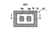
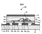
- FIG. 5A is a bottom view of the LED device 50 of the second embodiment
- FIG. 5B is a cross-sectional view taken along the line AA in FIG. 5A.
- the LED die 59, the phosphor layer 53, and the reflective layer 52 are arranged on the submount substrate 54 as in the LED device 1 of the first embodiment.
- the LED device 50 has the same external appearance as the LED device 1, a perspective view showing the external appearance of the LED device 50 is not shown (the perspective view showing the external appearance is also not shown in the embodiments described below).
- the bottom surface of the LED device 50 has a frame-shaped electrode 55 disposed in the periphery, and two inner electrodes 58 a and 58 b are disposed inside the frame-shaped electrode 55.
- the frame electrode 55 is connected to the ground wiring 57 a of the mother substrate 57 and is not connected to the LED die 59 mounted on the submount substrate 54.
- the inner electrode 58a is connected to the anode of the LED die 59 through the through hole 54d, the surface electrode 54a, and a wire.
- the inner electrode 58b is connected to the cathode of the LED die 59 through the through hole 54c, the surface electrode 54b, and the wire 59a.
- the frame-shaped electrode 55 formed around the bottom surface is at the ground level, and the frame-shaped electrode 55 is not connected to the LED die 59.
- the potential for impact is low.
- one LED die (LED die 9 (see FIG. 4) in the LED device 1) is mounted on the submount substrates 4 and 54.
- the number of LED dies mounted on the submount substrate is not limited to one.
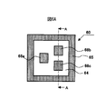
- An LED device 60 in which three LED dies are mounted on a submount substrate 64 will be described as a third embodiment with reference to FIGS. 6A, 6B, and 7.
- FIG. 6A is a bottom view of the LED device 60
- FIG. 6B is a cross-sectional view taken along the line AA in FIG. 6A
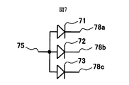
- FIG. 7 is a circuit diagram of the LED device 60.
- LED dies 71, 72, 73, a phosphor layer 63, and a reflective layer 62 are disposed on a submount substrate 64.
- a frame-shaped electrode 65 is disposed in the peripheral portion, and three inner electrodes 68 a, 68 b, 68 c are disposed inside the frame-shaped electrode 65.
- the three inner electrodes 68a, 68b, 68c are arranged in a triangle so as to form an isosceles triangle having the inner electrode 68a as a vertex and the inner electrodes 68b, 68c forming a base.
- the frame electrode 65 is a common electrode connected to the anodes of the LED dies 71, 72, 73, and the inner electrodes 68a, 68b, 68c are connected to the cathodes 78a, 78b, 78c of the LED dies 71, 72, 73, respectively. Is done.
- LED dies 71, 72, and 73 are a red light emitting diode, a green light emitting diode, and a blue light emitting diode, respectively.
- the LED dies 71, 72, and 73 share the anode 75 and are provided with cathodes 78a, 78b, and 78c, respectively.
- the anodes 75 of the LED dies 71, 72, and 73 are connected to the frame-shaped electrode 65 through the wire 69a, the surface electrode 64a, and the through hole 64c.
- the cathodes 78a, 78b, 78c of the LED dies 71, 72, 73 are connected to the inner electrodes 68a, 68b, 68c.
- the cathode 78b of the LED die 72 is connected to the inner electrode 68b through a wire, a surface electrode 642b, and a through hole 642d.
- the cathode 78c of the LED die 73 is connected to the inner electrode 68c through a wire, a surface electrode 643b, and a through hole 643d. Since the LED device 60 can individually control the currents flowing through the LED dies 71, 72, and 73, it is possible to emit various colors by changing the currents flowing through the LED dies 71, 72, and 73. .
- FIG. 8 is a bottom view of the LED device 80.
- the LED device 80 has the circuit configuration shown in FIG. 7 like the LED device 60 of the third embodiment.
- three LED dies 71, 72, 73 see FIG. 7
- a phosphor layer 83, and a reflective layer 82 are arranged on a submount substrate 84.
- a frame-like electrode 85 is arranged at the peripheral portion, and three inner electrodes 88 a, 88 b, 88 c are arranged in a line inside the frame-like electrode 85.
- the frame electrode 85 is a common electrode connected to the anodes of the LED dies 71, 72, 73.
- the anodes 75 of the LED dies 71, 72, and 73 are connected to the frame-shaped electrode 85 through wires 89a, surface electrodes 84a, and through holes 84c.
- the inner electrodes 88a, 88b, 88c are connected to the cathodes 78a, 78b, 78c of the LED dies 71, 72, 73, respectively.
- the cathode 78a of the LED die 71 is connected to the inner electrode 88a via a wire, a surface electrode 841b, and a through hole 841d.
- the cathode 78b of the LED die 72 is connected to the inner electrode 88b via a wire, a surface electrode 842b, and a through hole 842d.
- the cathode 78c of the LED die 73 is connected to the inner electrode 88c through a wire, a surface electrode 843b, and a through hole 843d.
- the frame-shaped electrodes 65 and 85 are connected to the anodes of the LED dies 71, 72, and 73.
- the frame-shaped electrode may not be connected to the anodes of the LED dies 71, 72, 73.
- LED devices 90, 100, and 110 in which the frame-like electrode is connected to the ground wiring of the mother board and not connected to the electrode of the LED die will be described as fifth, sixth, and seventh embodiments. .
- FIG. 9 are bottom views of the LED devices 90, 100 and 110, respectively.
- Each of the LED devices 90, 100, and 110 has the circuit configuration shown in FIG. 7 as in the LED device 60 of the third embodiment.
- three LED dies 71, 72, and 73 are disposed on the submount substrates 94, 104, and 114.
- the bottom surface of the LED device 90 has a frame-shaped electrode 95 arranged at the periphery, and four inner electrodes 98a, 98b, 98c, 98d are arranged in a line inside the frame-shaped electrode 95.
- the frame electrode 95 is connected to the ground wiring of the mother board, but is not connected to the electrodes of the LED dies 71, 72, 73. Any one of the inner electrodes 98a, 98b, 98c, 98d is connected to a common anode 75 (see FIG. 7), and the other inner electrodes are connected to the cathodes 78a, 78b, 78c of the LED dies 71, 72, 73, respectively. Connected.
- the bottom surface of the LED device 100 is arranged in a square so that the frame-like electrode 105 is arranged at the periphery, and the four inner electrodes 108a, 108b, 108c, 108d are positioned at the apexes of the square inside the frame-like electrode 105. Is done.
- the frame electrode 105 is connected to the ground wiring of the mother substrate, but is not connected to the electrodes of the LED dies 71, 72, 73. Any one of the inner electrodes 108a, 108b, 108c, 108d is connected to a common anode 75 (see FIG. 7), and the other inner electrodes are respectively connected to the cathodes 78a, 78b, 78c of the LED dies 71, 72, 73. Connected.
- a frame-shaped electrode 115 is arranged at the periphery, one inner electrode 118a inside the frame-shaped electrode 115, and three inner electrodes arranged in a row adjacent to the inner electrode 118a. 118b, 118c and 118d are arranged.
- the frame electrode 115 is connected to the ground wiring of the mother plate, but is not connected to the electrodes of the LED dies 71, 72, 73.
- the inner electrode 118a is connected to a common anode 75 (see FIG. 7), and each of the inner electrodes 118b, 118c, 118d is connected to the cathodes 78a, 78b, 78c of the LED dies 71, 72, 73.
- the frame-like electrode is formed over the entire outer peripheral portion of the bottom surface of the LED device.
- the periphery of the bottom surface of the LED device can be closed with solder along the outer peripheral portion when mounted on the mother board. Since the periphery of the bottom surface of the LED device is closed with solder along the outer peripheral portion, it is possible to prevent conductive foreign matters such as moisture from entering the bottom surface of the LED device without performing a special coating process.
- the inner electrode disposed inside the frame-shaped electrode is a through hole penetrating the mother substrate in order to cross the frame-shaped electrode.
- an LED device 120 that can connect the inner electrode to the wiring outside the frame electrode without using a through hole will be described as an eighth embodiment.
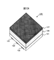
- FIG. 12A is a perspective view of the LED device 120
- FIG. 12B is a bottom view of the LED device 120.
- an LED die In the LED device 120, an LED die, a phosphor layer 128, and a reflective layer 127 are disposed on a submount substrate 121. Since the cross-sectional structure of the LED device 120 is substantially the same as the LED device 1 of the first embodiment, a cross-sectional view of the LED device 120 is not shown.
- the frame-like electrode 122 disposed on the bottom surface of the LED device 120 has three sides, an upper side, a left side extending downward from the left end of the upper side, and a right side extending downward from the right end of the upper side. It is formed in a shape in which one side of the shape is missing.
- the frame electrode 122 is formed in a U-shape.
- the frame-like electrode 122 includes electroplating patterns 122a, 122b, and 122c.
- the inner electrode 123 is formed so as to be surrounded by the frame electrode 122.
- the inner electrode 123 includes an electroplating pattern 123a.
- the submount substrate 121 is arranged on a large substrate in a state of being connected to each other at the time of manufacture, and is separated into pieces by cutting the large substrate. In a state where the plurality of LED devices 120 are arranged on the large-sized substrate, the electroplating pattern 122a and the electroplating pattern 122c are connected, and the electroplating pattern 122b and the electroplating pattern 123a are connected.
- FIG. 13 is a plan view showing a solder pattern formed on a mother board on which the LED device 120 is mounted.
- the solder pattern shown in FIG. 15 has a solder pattern 124 connected to the frame-shaped electrode 122 (see FIG. 12) and a solder pattern 125 connected to the inner electrode 123.
- the wiring on the mother substrate connected to the inner electrode 123 is formed so as to be connected to the solder pattern 125 from the opening side of the solder pattern 124.
- the LED device 120 can simplify the wiring of the mother board on which the LED device 120 is mounted. After the LED device 120 is mounted on the mother board, a protective member is applied only to the opening side of the solder pattern 124 (see FIG. 13) and coating is performed, so that foreign matter enters the bottom surface of the LED device 120. Is prevented. In the conventional LED device (see FIGS. 14 and 15), the entire outer periphery of the bottom surface of the LED device must be coated in order to prevent foreign matter from entering the bottom surface of the LED device. In apparatus 120, only one side of the bottom surface needs to be coated. Further, in comparison with the LED device 1 of the first embodiment in which the frame-like electrode 5 or the like (see FIG.
- the LED device 120 has a wiring of the inner electrode. There is no need to form a through hole in the mother substrate.
- the wiring of the mother substrate is simplified, so that the planar size of the submount substrate 121 (see FIG. 12) can be reduced, and the LED device 120 can be further downsized.
- a plurality of inner electrodes may be disposed in an LED device provided with a U-shaped frame electrode.
- the LED device may have a plurality of LED dies, and the emission colors of the LED dies mounted on the LED device are different from each other. May be.
- the reflective layer 2 is disposed on the top, and the phosphor layer 3 is disposed on the side.
- the structure of the element arranged on the surface on which the LED die of the submount substrate is arranged is not limited to the described embodiment.
- the LED die may be flip-chip mounted.
- the reflective layer disposed on the LED device may be removed.
- the reflecting member may be arranged on the side portion instead of the upper portion.
- the frame-shaped electrodes 5, 65, and 85 are connected to the anode of the LED die, and the inner electrodes 8, 68a to 68c and 88a to 88c are respectively Connected to the cathode of the LED die. That is, in the described embodiment, the inner electrode is connected to the cathode when the frame electrode is connected to the anode, and the inner electrode is connected to the anode when the frame electrode is connected to the cathode.
- the frame electrode may be connected to either the anode or the cathode, some inner electrodes may be connected to the anode, and some other inner electrodes may be connected to the cathode.
- the frame electrode 55 and the inner electrode 58a are connected to the anode of the LED die 9 (see FIG. 4), and the inner electrode 58b is connected to the cathode of the LED die 9. You may do it.
Landscapes
- Engineering & Computer Science (AREA)
- Microelectronics & Electronic Packaging (AREA)
- Power Engineering (AREA)
- Computer Hardware Design (AREA)
- Manufacturing & Machinery (AREA)
- Physics & Mathematics (AREA)
- Condensed Matter Physics & Semiconductors (AREA)
- General Physics & Mathematics (AREA)
- Led Device Packages (AREA)
Abstract
Description
図1は、第1実施形態のLED装置1の斜視図である。LED装置1は、最上部に配置される反射層2と、反射層2の下方に配置される蛍光体層3と、蛍光体層3の下方に配置されるサブマウント基板4と、サブマウント基板4の下方に配置される枠状電極5とを有する。
図1~4に示した第1実施形態のLED装置1では、枠状電極5がLEDダイ9のアノード又はカソードのどちらか一方の電極に接続し、内側電極8がカソード又はアノードの他方の電極に接続していた。しかしながら、実施形態のLED装置は、底面に配置された電極にアノード及びカソードに接続されるものの、枠状電極はアノード及びカソードの双方に接続されなくても良い。図5A及び5Bを参照して、枠状電極がアノード及びカソードの双方に接続されない第2実施形態のLED装置50を第2実施形態として説明する。
第1及び第2実施形態のLED装置1、50は、サブマウント基板4、54上に1個のLEDダイ(LED装置1ではLEDダイ9(図4参照))が実装される。しかしながら、サブマウント基板上に実装されるLEDダイの個数は、1個に限られない。図6A、6B及び図7を参照して、サブマウント基板64上に3個のLEDダイが実装されたLED装置60を第3実施形態として説明する。
第3実施形態のLED装置60では、内側電極68a、68b、68cは、三角配置される。しかしながら、内側電極の配置は、三角配置に限られない。図8を参照して、内側電極が直線状に配列されるLED装置80を第4実施形態として説明する。図8は、LED装置80の底面図である。LED装置80は、第3実施形態のLED装置60と同様に図7に示す回路構成を有する。LED装置80は、サブマウント基板84上に3個のLEDダイ71、72、73(図7参照)、蛍光体層83、及び反射層82が配置される。LED装置80の底面は、周辺部に枠状電極85が配置され、枠状電極85の内側に3個の内側電極88a、88b、88cが一列に並んで配置される。枠状電極85は、LEDダイ71、72、73のアノードに接続される共通電極である。LEDダイ71、72、73のアノード75は、ワイヤ89a、表面電極84a及びスルーホール84cを介して枠状電極85に接続される。内側電極88a、88b、88cはそれぞれ、LEDダイ71、72、73のカソード78a、78b、78cに接続される。LEDダイ71のカソード78aは、ワイヤ、表面電極841b及びスルーホール841dを介して内側電極88aに接続される。LEDダイ72のカソード78bは、ワイヤ、表面電極842b及びスルーホール842dを介して内側電極88bに接続される。LEDダイ73のカソード78cは、ワイヤ、表面電極843b及びスルーホール843dを介して内側電極88cに接続される。
第3、4実施形態のLED装置60、80では、枠状電極65、85はLEDダイ71、72、73のアノードに接続される。しかしながら、実施形態のLED装置では、枠状電極はLEDダイ71、72、73のアノードに接続されなくても良い。図9、10、11を参照して、枠状電極がマザー基板のグランド配線に接続され且つLEDダイの電極に接続されないLED装置90、100、110を第5、6、7実施形態として説明する。
第1~7実施形態のLED装置1、50、60、80、90、100、110では、枠状電極がLED装置の底面の外周部全体に亘って形成される。枠状電極をLED装置の底面の外周部全体に亘って形成することにより、マザー基板に実装したときにLED装置の底面の周囲を外周部に沿ってハンダで塞ぐことができる。LED装置の底面の周囲を外周部に沿ってハンダで塞ぐので、特別なコーティングティング処理を施すことなく、水分等の導電性の異物がLED装置の底面に侵入することを防ぐことができる。しかしながら、LED装置の底面の外周部全体に亘って枠状電極が配置される場合、枠状電極を横切るために、枠状電極の内側に配置される内側電極は、マザー基板を貫通するスルーホールを介して枠状電極の外側の配線に接続される。図12A、12B及び13を参照して、スルーホールを使用することなしに内側電極を枠状電極の外側の配線に接続可能なLED装置120を第8実施形態として説明する。
2,52,62,82,127 反射層
3,53,63,83,128 蛍光体層
4,54,64,84,94,104,114,121 サブマウント基板
4a,4b,54a,54b,64a,642b,643b,84a,841b,842b,843b 表面電極
4c,4d,54c,54d,64c,642d,643d,84c,841d,842d,843d, スルーホール
5,55,65,85,95,105,115,122 枠状電極
6,6a,56,56a,56b,66,662,663,86,861,862,863 ハンダ
7,57,67,87 マザー基板
7a,7b,57a,57b,57c,67a,672b,673b,87a,871b,872b,873b 配線電極
8,58a,58b,68a~c,88a~c,98a~d,108a~d,118a~d,123 内側電極
9,59,71,72,73 LEDダイ
9a,59a,69a,89a ワイヤ
75 アノード
78a,78b,78c カソード
122a,122b,122c,123a 電界めっき用パターン
124,125 ハンダパターン
Claims (7)
- LEDダイと、
表面に前記LEDダイが実装されたサブマウント基板と、
前記サブマウント基板の底面の外周部に沿って配置された枠状電極と、
前記枠状電極に囲まれ且つ前記LEDダイの電極に接続された内側電極と、
を有することを特徴とするLED装置。 - 前記枠状電極は、前記底面の外周部の全体に亘って配置されている、請求項1に記載のLED装置。
- 前記底面の形状は矩形であり、
前記枠状電極は、前記底面の3辺に沿って配置されている、請求項1に記載のLED装置。 - 前記枠状電極は、前記LEDダイの電極に接続されている、請求項1~3の何れか一項に記載のLED装置。
- 前記
前記枠状電極は、前記LED装置が搭載されたマザー基板に形成されたグランド配線に接続されている、請求項1~3の何れか一項に記載のLED装置。 - 少なくとも2つの前記内側電極を有する、請求項1~5の何れか一項に記載のLED装置。
- 前記LEDダイが、赤色発光LEDダイ、緑色発光LEDダイ及び青色発光LEDダイである、請求項1~6の何れか一項に記載のLED装置。
Priority Applications (4)
| Application Number | Priority Date | Filing Date | Title |
|---|---|---|---|
| EP14817164.8A EP3016154B1 (en) | 2013-06-28 | 2014-06-23 | Led device |
| JP2014544288A JP5693800B1 (ja) | 2013-06-28 | 2014-06-23 | Led装置 |
| US14/901,471 US10170674B2 (en) | 2013-06-28 | 2014-06-23 | LED device |
| CN201480037154.6A CN105359284B (zh) | 2013-06-28 | 2014-06-23 | Led装置 |
Applications Claiming Priority (4)
| Application Number | Priority Date | Filing Date | Title |
|---|---|---|---|
| JP2013136338 | 2013-06-28 | ||
| JP2013-136338 | 2013-06-28 | ||
| JP2013-173114 | 2013-08-23 | ||
| JP2013173114 | 2013-08-23 |
Publications (1)
| Publication Number | Publication Date |
|---|---|
| WO2014208495A1 true WO2014208495A1 (ja) | 2014-12-31 |
Family
ID=52141830
Family Applications (1)
| Application Number | Title | Priority Date | Filing Date |
|---|---|---|---|
| PCT/JP2014/066540 WO2014208495A1 (ja) | 2013-06-28 | 2014-06-23 | Led装置 |
Country Status (5)
| Country | Link |
|---|---|
| US (1) | US10170674B2 (ja) |
| EP (1) | EP3016154B1 (ja) |
| JP (1) | JP5693800B1 (ja) |
| CN (1) | CN105359284B (ja) |
| WO (1) | WO2014208495A1 (ja) |
Cited By (4)
| Publication number | Priority date | Publication date | Assignee | Title |
|---|---|---|---|---|
| WO2019235565A1 (ja) * | 2018-06-08 | 2019-12-12 | 日機装株式会社 | 半導体発光装置 |
| JP2021082849A (ja) * | 2019-05-30 | 2021-05-27 | 日亜化学工業株式会社 | 発光モジュール |
| CN113314943A (zh) * | 2020-02-26 | 2021-08-27 | 富士胶片商业创新有限公司 | 发光装置、光学装置以及信息处理装置 |
| KR20230002169A (ko) * | 2019-05-30 | 2023-01-05 | 니치아 카가쿠 고교 가부시키가이샤 | 발광 모듈 및 그 제조방법 |
Families Citing this family (4)
| Publication number | Priority date | Publication date | Assignee | Title |
|---|---|---|---|---|
| JP5693800B1 (ja) * | 2013-06-28 | 2015-04-01 | シチズンホールディングス株式会社 | Led装置 |
| TWI575785B (zh) * | 2014-10-30 | 2017-03-21 | 新世紀光電股份有限公司 | 發光裝置 |
| TWI684835B (zh) | 2018-12-25 | 2020-02-11 | 同泰電子科技股份有限公司 | 具有高反射率的基板結構及其製作方法 |
| WO2022061770A1 (zh) * | 2020-09-25 | 2022-03-31 | 京东方科技集团股份有限公司 | 一种柔性线路板、灯条、背光模组及液晶显示装置 |
Citations (5)
| Publication number | Priority date | Publication date | Assignee | Title |
|---|---|---|---|---|
| JPS6352422A (ja) * | 1986-08-22 | 1988-03-05 | Hitachi Tobu Semiconductor Ltd | 電子装置およびそのチツプならびにその基板 |
| JP2005191097A (ja) | 2003-12-24 | 2005-07-14 | Kawaguchiko Seimitsu Co Ltd | 半導体パッケージ |
| JP2009130237A (ja) * | 2007-11-27 | 2009-06-11 | Panasonic Corp | 発光装置 |
| WO2012022782A1 (de) * | 2010-08-20 | 2012-02-23 | Osram Opto Semiconductors Gmbh | Optoelektronisches halbleiterbauelement |
| JP2012044218A (ja) * | 2005-10-31 | 2012-03-01 | Toyoda Gosei Co Ltd | 発光装置 |
Family Cites Families (23)
| Publication number | Priority date | Publication date | Assignee | Title |
|---|---|---|---|---|
| US9070850B2 (en) * | 2007-10-31 | 2015-06-30 | Cree, Inc. | Light emitting diode package and method for fabricating same |
| US20070080360A1 (en) * | 2005-10-06 | 2007-04-12 | Url Mirsky | Microelectronic interconnect substrate and packaging techniques |
| JP4940883B2 (ja) | 2005-10-31 | 2012-05-30 | 豊田合成株式会社 | 発光装置 |
| US7928462B2 (en) * | 2006-02-16 | 2011-04-19 | Lg Electronics Inc. | Light emitting device having vertical structure, package thereof and method for manufacturing the same |
| CN101304059B (zh) * | 2007-05-09 | 2010-09-08 | 富士迈半导体精密工业(上海)有限公司 | 发光二极管组件及发光二极管显示装置 |
| US8436371B2 (en) * | 2007-05-24 | 2013-05-07 | Cree, Inc. | Microscale optoelectronic device packages |
| US9172012B2 (en) * | 2007-10-31 | 2015-10-27 | Cree, Inc. | Multi-chip light emitter packages and related methods |
| JP5345363B2 (ja) * | 2008-06-24 | 2013-11-20 | シャープ株式会社 | 発光装置 |
| WO2011083923A2 (en) * | 2010-01-07 | 2011-07-14 | Seoul Opto Device Co., Ltd. | Light emitting diode having electrode pads |
| WO2012016377A1 (en) | 2010-08-03 | 2012-02-09 | Industrial Technology Research Institute | Light emitting diode chip, light emitting diode package structure, and method for forming the same |
| EP2418700B1 (en) * | 2010-08-09 | 2017-11-01 | LG Innotek Co., Ltd. | Light emitting device |
| KR20120082190A (ko) * | 2011-01-13 | 2012-07-23 | 삼성엘이디 주식회사 | 발광소자 패키지 |
| US9240524B2 (en) * | 2012-03-05 | 2016-01-19 | Seoul Viosys Co., Ltd. | Light-emitting device and method of manufacturing the same |
| JP5989388B2 (ja) * | 2012-04-19 | 2016-09-07 | 新光電気工業株式会社 | パッケージ及びパッケージの製造方法 |
| US20130328074A1 (en) * | 2012-06-11 | 2013-12-12 | Cree, Inc. | Led package with multiple element light source and encapsulant having planar surfaces |
| JP6138814B2 (ja) * | 2012-10-24 | 2017-05-31 | シャープ株式会社 | 発光装置および発光装置の製造方法 |
| CN202996902U (zh) * | 2012-11-21 | 2013-06-12 | 深圳市斯迈得光电子有限公司 | 一种安全可靠的led灯珠 |
| KR20140094752A (ko) * | 2013-01-22 | 2014-07-31 | 삼성전자주식회사 | 전자소자 패키지 및 이에 사용되는 패키지 기판 |
| DE102013104840A1 (de) * | 2013-05-10 | 2014-11-13 | Osram Opto Semiconductors Gmbh | Strahlungsemittierendes Halbleiterbauelement und Verfahren zur Herstellung von strahlungsemittierenden Halbleiterbauelementen |
| JP5693800B1 (ja) * | 2013-06-28 | 2015-04-01 | シチズンホールディングス株式会社 | Led装置 |
| GB201400264D0 (en) | 2014-01-08 | 2014-02-26 | Element Six Ltd | Synthetic diamond optical mirrors |
| KR20160023011A (ko) * | 2014-08-20 | 2016-03-03 | 삼성전자주식회사 | 발광소자 패키지 |
| EP2988341B1 (en) * | 2014-08-22 | 2017-04-05 | LG Innotek Co., Ltd. | Light emitting device package |
-
2014
- 2014-06-23 JP JP2014544288A patent/JP5693800B1/ja active Active
- 2014-06-23 CN CN201480037154.6A patent/CN105359284B/zh active Active
- 2014-06-23 WO PCT/JP2014/066540 patent/WO2014208495A1/ja active Application Filing
- 2014-06-23 US US14/901,471 patent/US10170674B2/en active Active
- 2014-06-23 EP EP14817164.8A patent/EP3016154B1/en active Active
Patent Citations (5)
| Publication number | Priority date | Publication date | Assignee | Title |
|---|---|---|---|---|
| JPS6352422A (ja) * | 1986-08-22 | 1988-03-05 | Hitachi Tobu Semiconductor Ltd | 電子装置およびそのチツプならびにその基板 |
| JP2005191097A (ja) | 2003-12-24 | 2005-07-14 | Kawaguchiko Seimitsu Co Ltd | 半導体パッケージ |
| JP2012044218A (ja) * | 2005-10-31 | 2012-03-01 | Toyoda Gosei Co Ltd | 発光装置 |
| JP2009130237A (ja) * | 2007-11-27 | 2009-06-11 | Panasonic Corp | 発光装置 |
| WO2012022782A1 (de) * | 2010-08-20 | 2012-02-23 | Osram Opto Semiconductors Gmbh | Optoelektronisches halbleiterbauelement |
Non-Patent Citations (1)
| Title |
|---|
| See also references of EP3016154A4 * |
Cited By (12)
| Publication number | Priority date | Publication date | Assignee | Title |
|---|---|---|---|---|
| WO2019235565A1 (ja) * | 2018-06-08 | 2019-12-12 | 日機装株式会社 | 半導体発光装置 |
| US11677052B2 (en) | 2018-06-08 | 2023-06-13 | Nikkiso Co., Ltd. | Semiconductor light-emitting device |
| JP2021082849A (ja) * | 2019-05-30 | 2021-05-27 | 日亜化学工業株式会社 | 発光モジュール |
| KR20230002169A (ko) * | 2019-05-30 | 2023-01-05 | 니치아 카가쿠 고교 가부시키가이샤 | 발광 모듈 및 그 제조방법 |
| JP7236630B2 (ja) | 2019-05-30 | 2023-03-10 | 日亜化学工業株式会社 | 発光モジュール |
| US11681090B2 (en) | 2019-05-30 | 2023-06-20 | Nichia Corporation | Light emitting module and method of manufacturing same |
| KR102620488B1 (ko) | 2019-05-30 | 2024-01-02 | 니치아 카가쿠 고교 가부시키가이샤 | 발광 모듈 및 그 제조방법 |
| US12050338B2 (en) | 2019-05-30 | 2024-07-30 | Nichia Corporation | Light emitting module and method of manufacturing same |
| CN113314943A (zh) * | 2020-02-26 | 2021-08-27 | 富士胶片商业创新有限公司 | 发光装置、光学装置以及信息处理装置 |
| JP2021136305A (ja) * | 2020-02-26 | 2021-09-13 | 富士フイルムビジネスイノベーション株式会社 | 発光装置、光学装置及び情報処理装置 |
| JP7497578B2 (ja) | 2020-02-26 | 2024-06-11 | 富士フイルムビジネスイノベーション株式会社 | 発光装置、光学装置及び情報処理装置 |
| US12057677B2 (en) | 2020-02-26 | 2024-08-06 | Fujifilm Business Innovation Corp. | Light-emitting device, optical device, and information processing apparatus |
Also Published As
| Publication number | Publication date |
|---|---|
| EP3016154A4 (en) | 2016-12-14 |
| US20160197253A1 (en) | 2016-07-07 |
| JP5693800B1 (ja) | 2015-04-01 |
| EP3016154B1 (en) | 2020-08-05 |
| JPWO2014208495A1 (ja) | 2017-02-23 |
| US10170674B2 (en) | 2019-01-01 |
| CN105359284B (zh) | 2019-05-14 |
| EP3016154A1 (en) | 2016-05-04 |
| CN105359284A (zh) | 2016-02-24 |
Similar Documents
| Publication | Publication Date | Title |
|---|---|---|
| JP5693800B1 (ja) | Led装置 | |
| US9035333B2 (en) | Semiconductor light emitting device | |
| JP6131048B2 (ja) | Ledモジュール | |
| US10263159B2 (en) | Light-emitter mounting package, light-emitting device, and light-emitting module | |
| JP2004253404A (ja) | 発光素子収納用パッケージおよび発光装置 | |
| CN104752585A (zh) | 集合基板、发光装置及发光元件的检查方法 | |
| KR101986855B1 (ko) | 발광 부품용 회로와 그 제조 방법 | |
| US20160172558A1 (en) | Led flip chip structures with extended contact pads formed by sintering silver | |
| US9537019B2 (en) | Semiconductor device | |
| JP2013012666A (ja) | 発光装置の製造方法 | |
| JP2004319939A (ja) | 発光素子収納用パッケージおよび発光装置 | |
| JP2008078401A (ja) | 照明装置 | |
| JP2011233775A (ja) | 半導体パッケージおよび半導体発光装置 | |
| JP2004228413A (ja) | 発光素子収納用パッケージおよび発光装置 | |
| JP2019216250A (ja) | 半導体発光装置 | |
| JP4163982B2 (ja) | 発光素子収納用パッケージおよび発光装置 | |
| JP2004253711A (ja) | 発光素子収納用パッケージおよび発光装置 | |
| JP6626735B2 (ja) | 電子部品搭載用基板、電子装置および電子モジュール | |
| JP2013105826A (ja) | 半導体発光装置及びそれを備えた電子機器並びにその製造方法 | |
| JP5913432B2 (ja) | チップ型発光素子 | |
| JP5809440B2 (ja) | Ledモジュール | |
| US7923747B2 (en) | Wafer level LED package structure and method for making the same | |
| KR20140110257A (ko) | 발광소자 패키지 | |
| JP2016018990A (ja) | パッケージ構造及びその製法並びに搭載部材 | |
| JP6486726B2 (ja) | 発光モジュール |
Legal Events
| Date | Code | Title | Description |
|---|---|---|---|
| WWE | Wipo information: entry into national phase |
Ref document number: 201480037154.6 Country of ref document: CN |
|
| ENP | Entry into the national phase |
Ref document number: 2014544288 Country of ref document: JP Kind code of ref document: A |
|
| 121 | Ep: the epo has been informed by wipo that ep was designated in this application |
Ref document number: 14817164 Country of ref document: EP Kind code of ref document: A1 |
|
| WWE | Wipo information: entry into national phase |
Ref document number: 2014817164 Country of ref document: EP |
|
| NENP | Non-entry into the national phase |
Ref country code: DE |
|
| WWE | Wipo information: entry into national phase |
Ref document number: 14901471 Country of ref document: US |