WO2014196330A1 - 有機エレクトロルミネッセンス素子 - Google Patents
有機エレクトロルミネッセンス素子 Download PDFInfo
- Publication number
- WO2014196330A1 WO2014196330A1 PCT/JP2014/062916 JP2014062916W WO2014196330A1 WO 2014196330 A1 WO2014196330 A1 WO 2014196330A1 JP 2014062916 W JP2014062916 W JP 2014062916W WO 2014196330 A1 WO2014196330 A1 WO 2014196330A1
- Authority
- WO
- WIPO (PCT)
- Prior art keywords
- layer
- organic
- group
- transparent
- transparent electrode
- Prior art date
- Legal status (The legal status is an assumption and is not a legal conclusion. Google has not performed a legal analysis and makes no representation as to the accuracy of the status listed.)
- Ceased
Links
- 0 CC(C1C=C2)(C=C2c(cccc2)c2-c2ccccn2)c2ncccc2N1c1cc(-[n](c(c2c3)ccc3-c(cccc3)c3-c3ncccc3)c3c2N(C)CC=C3)cc(-[n]2c3cccnc3c3c2ccc(-c2c(*C=CC=CN)cccc2)c3)c1 Chemical compound CC(C1C=C2)(C=C2c(cccc2)c2-c2ccccn2)c2ncccc2N1c1cc(-[n](c(c2c3)ccc3-c(cccc3)c3-c3ncccc3)c3c2N(C)CC=C3)cc(-[n]2c3cccnc3c3c2ccc(-c2c(*C=CC=CN)cccc2)c3)c1 0.000 description 2
- VLNWWTIIWPNFKN-UHFFFAOYSA-N c(cc1)cc(-c(cc2c3c4cccn3)ccc2[n]4-c2cccc(-[n]3c4cccnc4c4c3ccc(-c3ccccc3-c3ccccn3)c4)c2)c1-c1ccccn1 Chemical compound c(cc1)cc(-c(cc2c3c4cccn3)ccc2[n]4-c2cccc(-[n]3c4cccnc4c4c3ccc(-c3ccccc3-c3ccccn3)c4)c2)c1-c1ccccn1 VLNWWTIIWPNFKN-UHFFFAOYSA-N 0.000 description 2
- TYJXCEAGLDGNMT-UHFFFAOYSA-N C(C1)C=Nc(c2cc(-c3ccccc3-c3ncccc3)ccc22)c1[n]2-c1cncc(-[n]2c3cccnc3c3c2ccc(-c(cccc2)c2-c2ccccn2)c3)c1 Chemical compound C(C1)C=Nc(c2cc(-c3ccccc3-c3ncccc3)ccc22)c1[n]2-c1cncc(-[n]2c3cccnc3c3c2ccc(-c(cccc2)c2-c2ccccn2)c3)c1 TYJXCEAGLDGNMT-UHFFFAOYSA-N 0.000 description 1
- RODFURIYXWMADV-UHFFFAOYSA-N C(C12)=CC=NC1c(cc(cc1)-c3ccccc3-c3ncccc3)c1N2c1cccc(-[n]2c3cccnc3c3c2ccc(-c(cccc2)c2-c2ccccn2)c3)n1 Chemical compound C(C12)=CC=NC1c(cc(cc1)-c3ccccc3-c3ncccc3)c1N2c1cccc(-[n]2c3cccnc3c3c2ccc(-c(cccc2)c2-c2ccccn2)c3)n1 RODFURIYXWMADV-UHFFFAOYSA-N 0.000 description 1
- GWIAVISXYNKAAQ-UHFFFAOYSA-N CC(CC(c1cncc(-c2cc(-c3ncccc3)cc(-c3ccccn3)c2)c1)=C1)(C=C1c1ncccc1)c1ccccn1 Chemical compound CC(CC(c1cncc(-c2cc(-c3ncccc3)cc(-c3ccccn3)c2)c1)=C1)(C=C1c1ncccc1)c1ccccn1 GWIAVISXYNKAAQ-UHFFFAOYSA-N 0.000 description 1
- SNACRBVZZHLETL-UHFFFAOYSA-N CN(C1)C=Cc2c1c1cnccc1[n]2-c1cc(-[n]2c3ccncc3c3cnccc23)ccc1 Chemical compound CN(C1)C=Cc2c1c1cnccc1[n]2-c1cc(-[n]2c3ccncc3c3cnccc23)ccc1 SNACRBVZZHLETL-UHFFFAOYSA-N 0.000 description 1
- QUPREZZOOOBGHL-UHFFFAOYSA-N CN1C(c2cc(-c(cc3-c4ncccc4)cc(-c4ncccc4)c3-c3ncccc3)cc(-c3ncccc3)c2-c2ncccc2)=CC=CC1 Chemical compound CN1C(c2cc(-c(cc3-c4ncccc4)cc(-c4ncccc4)c3-c3ncccc3)cc(-c3ncccc3)c2-c2ncccc2)=CC=CC1 QUPREZZOOOBGHL-UHFFFAOYSA-N 0.000 description 1
- IXKPHJWMEWCNJZ-UHFFFAOYSA-N CN1C=CC=CC1c(c1c(cc2-c3ccccn3)c(cc(-c3ncccc3)c(-c3ncccc3)c3-c4ncccc4)c3[s]1)c2-c1ccccn1 Chemical compound CN1C=CC=CC1c(c1c(cc2-c3ccccn3)c(cc(-c3ncccc3)c(-c3ncccc3)c3-c4ncccc4)c3[s]1)c2-c1ccccn1 IXKPHJWMEWCNJZ-UHFFFAOYSA-N 0.000 description 1
- FLGYPUOBEXJTQI-UHFFFAOYSA-N CN1C=CC=CC1c(ccc(-c(cc1)cc(-c2cncnc2)c1-c1ccccn1)c1)c1C1=CNCNC1 Chemical compound CN1C=CC=CC1c(ccc(-c(cc1)cc(-c2cncnc2)c1-c1ccccn1)c1)c1C1=CNCNC1 FLGYPUOBEXJTQI-UHFFFAOYSA-N 0.000 description 1
- YGMGSPPHYXJIDW-UHFFFAOYSA-N Cc(cc(cc1)-[n](c(c2c3)ccc3Br)c3c2nccc3)c1-c(cc1)c(C)cc1-[n]1c2cccnc2c2c1ccc(Br)c2 Chemical compound Cc(cc(cc1)-[n](c(c2c3)ccc3Br)c3c2nccc3)c1-c(cc1)c(C)cc1-[n]1c2cccnc2c2c1ccc(Br)c2 YGMGSPPHYXJIDW-UHFFFAOYSA-N 0.000 description 1
- VYHKBDVTDPZQKP-UHFFFAOYSA-N Cc1cc(-[n]2c(ccnc3)c3c3c2ccnc3)ccc1-c(cc1)c(C)cc1-[n]1c2ccncc2c2c1ccnc2 Chemical compound Cc1cc(-[n]2c(ccnc3)c3c3c2ccnc3)ccc1-c(cc1)c(C)cc1-[n]1c2ccncc2c2c1ccnc2 VYHKBDVTDPZQKP-UHFFFAOYSA-N 0.000 description 1
- OGGKVJMNFFSDEV-UHFFFAOYSA-N Cc1cccc(N(c2ccccc2)c(cc2)ccc2-c(cc2)ccc2N(c2ccccc2)c2cccc(C)c2)c1 Chemical compound Cc1cccc(N(c2ccccc2)c(cc2)ccc2-c(cc2)ccc2N(c2ccccc2)c2cccc(C)c2)c1 OGGKVJMNFFSDEV-UHFFFAOYSA-N 0.000 description 1
- RHGXLEMFSRCEIU-UHFFFAOYSA-N c(c(-c1cncc(-c2cc(-c3cncnc3)cc(-c3cncnc3)c2)c1)cc(-c1cncnc1)c1)c1-c1cncnc1 Chemical compound c(c(-c1cncc(-c2cc(-c3cncnc3)cc(-c3cncnc3)c2)c1)cc(-c1cncnc1)c1)c1-c1cncnc1 RHGXLEMFSRCEIU-UHFFFAOYSA-N 0.000 description 1
- CUMXWFMPRBCSDF-UHFFFAOYSA-N c(cc1)cc(-c(cc2c3cc(-c(cccc4)c4-c4ccccn4)ccc33)ccc2[n]3-c(cc2)cc3c2[s]c(cc2)c3cc2-c(cccc2)c2-c2ncccc2)c1-c1ncccc1 Chemical compound c(cc1)cc(-c(cc2c3cc(-c(cccc4)c4-c4ccccn4)ccc33)ccc2[n]3-c(cc2)cc3c2[s]c(cc2)c3cc2-c(cccc2)c2-c2ncccc2)c1-c1ncccc1 CUMXWFMPRBCSDF-UHFFFAOYSA-N 0.000 description 1
- FNCJNJFJTCYRLB-UHFFFAOYSA-N c(cc1)cc(c2c3cccc2)c1[n]3-c(cc1)cc(c2c3)c1[o]c2ccc3-c(cc1)cc2c1[o]c1cccnc21 Chemical compound c(cc1)cc(c2c3cccc2)c1[n]3-c(cc1)cc(c2c3)c1[o]c2ccc3-c(cc1)cc2c1[o]c1cccnc21 FNCJNJFJTCYRLB-UHFFFAOYSA-N 0.000 description 1
- USXYLPLRYKAFHX-UHFFFAOYSA-N c(cc1)cc(c2cc(-c(cccc3)c3-c3ccccn3)ccc22)c1[n]2-c(cc1)cc(c2c3)c1[s]c2ccc3-c(cccc1)c1-c1ncccc1 Chemical compound c(cc1)cc(c2cc(-c(cccc3)c3-c3ccccn3)ccc22)c1[n]2-c(cc1)cc(c2c3)c1[s]c2ccc3-c(cccc1)c1-c1ncccc1 USXYLPLRYKAFHX-UHFFFAOYSA-N 0.000 description 1
- JBCTXOVZGVAKQI-UHFFFAOYSA-N c(cc1)ccc1-[n](c(cc(c(-c1ccccn1)c1)-c2ccccn2)c1c1c2)c1cc(-c1ccccn1)c2-c1ncccc1 Chemical compound c(cc1)ccc1-[n](c(cc(c(-c1ccccn1)c1)-c2ccccn2)c1c1c2)c1cc(-c1ccccn1)c2-c1ncccc1 JBCTXOVZGVAKQI-UHFFFAOYSA-N 0.000 description 1
- VKWYPRUZNQNNED-UHFFFAOYSA-N c(cc1)ccc1-[n]1c(ccc(-c(cccc2)c2-c2ncccc2)c2)c2c2cc(-c(cc3)cc(c4cc(-c(cccc5)c5-c5ccccn5)ccc44)c3[n]4-c3ccccc3)ccc12 Chemical compound c(cc1)ccc1-[n]1c(ccc(-c(cccc2)c2-c2ncccc2)c2)c2c2cc(-c(cc3)cc(c4cc(-c(cccc5)c5-c5ccccn5)ccc44)c3[n]4-c3ccccc3)ccc12 VKWYPRUZNQNNED-UHFFFAOYSA-N 0.000 description 1
- FMWSXZWOXCBFCE-UHFFFAOYSA-N c(cc1-c(cc2c3c4cccn3)ccc2[n]4-c2nc(-c3ncccc3)ccc2)ccc1-c1ncccc1 Chemical compound c(cc1-c(cc2c3c4cccn3)ccc2[n]4-c2nc(-c3ncccc3)ccc2)ccc1-c1ncccc1 FMWSXZWOXCBFCE-UHFFFAOYSA-N 0.000 description 1
- DHVMHCSQFVLMJI-UHFFFAOYSA-N c(cc1c2c3)ccc1[s]c2ccc3-[n](c(ccc(-c1ccccc1-c1ncccc1)c1)c1c1c2)c1ccc2-c(cccc1)c1-c1ncccc1 Chemical compound c(cc1c2c3)ccc1[s]c2ccc3-[n](c(ccc(-c1ccccc1-c1ncccc1)c1)c1c1c2)c1ccc2-c(cccc1)c1-c1ncccc1 DHVMHCSQFVLMJI-UHFFFAOYSA-N 0.000 description 1
- XZEXNDNIJFWTBX-UHFFFAOYSA-N c(cc1c2c3ccc(-c4ccccc4-c4ccccn4)c2)ccc1[n]3-c1ccc2[s]c(ccc(-[n](c(ccc(-c(cccc3)c3-c3ccccn3)c3)c3c3c4)c3ccc4-c(cccc3)c3-c3ccccn3)c3)c3c2c1 Chemical compound c(cc1c2c3ccc(-c4ccccc4-c4ccccn4)c2)ccc1[n]3-c1ccc2[s]c(ccc(-[n](c(ccc(-c(cccc3)c3-c3ccccn3)c3)c3c3c4)c3ccc4-c(cccc3)c3-c3ccccn3)c3)c3c2c1 XZEXNDNIJFWTBX-UHFFFAOYSA-N 0.000 description 1
- OMOOGNAWWQVAJL-UHFFFAOYSA-N c1cc(-c(cc2)cc(c3cc(-c4ncccc4)ccc33)c2[n]3-c2cc(-[n]3c(ccc(-c4ncccc4)c4)c4c4cc(-c5ccccn5)ccc34)ccc2)ncc1 Chemical compound c1cc(-c(cc2)cc(c3cc(-c4ncccc4)ccc33)c2[n]3-c2cc(-[n]3c(ccc(-c4ncccc4)c4)c4c4cc(-c5ccccn5)ccc34)ccc2)ncc1 OMOOGNAWWQVAJL-UHFFFAOYSA-N 0.000 description 1
- GBBWFJZXZXHHDD-UHFFFAOYSA-N c1cc(-c2cc(-c(cc3)ccc3-c3cc(-c4ccccn4)nc(-c4ncccc4)c3)cc(-c3ccccn3)c2)ncc1 Chemical compound c1cc(-c2cc(-c(cc3)ccc3-c3cc(-c4ccccn4)nc(-c4ncccc4)c3)cc(-c3ccccn3)c2)ncc1 GBBWFJZXZXHHDD-UHFFFAOYSA-N 0.000 description 1
- UWGYFPNYYRLEHS-UHFFFAOYSA-N c1cc(-c2cc(-c3cc(-c4cc(-c5ccccn5)nc(-c5ncccc5)c4)ccc3)cc(-c3ccccn3)n2)ncc1 Chemical compound c1cc(-c2cc(-c3cc(-c4cc(-c5ccccn5)nc(-c5ncccc5)c4)ccc3)cc(-c3ccccn3)n2)ncc1 UWGYFPNYYRLEHS-UHFFFAOYSA-N 0.000 description 1
- ZBAIOOJCIIDLBE-UHFFFAOYSA-N c1cc(-c2cccc(-c(cc3)cc(c4cc(-c5cc(-c6ncccc6)ccc5)ccc44)c3[n]4-c3cc(-[n](c(c(c4c5)c6)ccc6-c6cccc(-c7ccccn7)c6)c4ccc5-c4cc(-c5ccccn5)ccc4)ccc3)c2)ncc1 Chemical compound c1cc(-c2cccc(-c(cc3)cc(c4cc(-c5cc(-c6ncccc6)ccc5)ccc44)c3[n]4-c3cc(-[n](c(c(c4c5)c6)ccc6-c6cccc(-c7ccccn7)c6)c4ccc5-c4cc(-c5ccccn5)ccc4)ccc3)c2)ncc1 ZBAIOOJCIIDLBE-UHFFFAOYSA-N 0.000 description 1
- KMVWNDHKTPHDMT-UHFFFAOYSA-N c1cc(-c2nc(-c3ccccn3)nc(-c3ncccc3)n2)ncc1 Chemical compound c1cc(-c2nc(-c3ccccn3)nc(-c3ncccc3)n2)ncc1 KMVWNDHKTPHDMT-UHFFFAOYSA-N 0.000 description 1
- PTYQXXWJISYYFP-UHFFFAOYSA-N c1ccnc(-c(cc2-c3ccccn3)c(-c3ccccn3)c(-c3ccccn3)c2-c2ccccn2)c1 Chemical compound c1ccnc(-c(cc2-c3ccccn3)c(-c3ccccn3)c(-c3ccccn3)c2-c2ccccn2)c1 PTYQXXWJISYYFP-UHFFFAOYSA-N 0.000 description 1
- TZTWVVFUYVGVDU-UHFFFAOYSA-N c1cncc(c2cnccc22)c1[n]2-c(cc1)ccc1-[n]1c(ccnc2)c2c2c1ccnc2 Chemical compound c1cncc(c2cnccc22)c1[n]2-c(cc1)ccc1-[n]1c(ccnc2)c2c2c1ccnc2 TZTWVVFUYVGVDU-UHFFFAOYSA-N 0.000 description 1
- CBMYFVSIIYILRH-UHFFFAOYSA-N c1cnccc1-c1nc(-c2ccncc2)nc(-c2ccncc2)n1 Chemical compound c1cnccc1-c1nc(-c2ccncc2)nc(-c2ccncc2)n1 CBMYFVSIIYILRH-UHFFFAOYSA-N 0.000 description 1
Images

Classifications
-
- C—CHEMISTRY; METALLURGY
- C09—DYES; PAINTS; POLISHES; NATURAL RESINS; ADHESIVES; COMPOSITIONS NOT OTHERWISE PROVIDED FOR; APPLICATIONS OF MATERIALS NOT OTHERWISE PROVIDED FOR
- C09K—MATERIALS FOR MISCELLANEOUS APPLICATIONS, NOT PROVIDED FOR ELSEWHERE
- C09K11/00—Luminescent materials, e.g. electroluminescent or chemiluminescent
- C09K11/06—Luminescent materials, e.g. electroluminescent or chemiluminescent containing organic luminescent materials
-
- H—ELECTRICITY
- H10—SEMICONDUCTOR DEVICES; ELECTRIC SOLID-STATE DEVICES NOT OTHERWISE PROVIDED FOR
- H10K—ORGANIC ELECTRIC SOLID-STATE DEVICES
- H10K50/00—Organic light-emitting devices
- H10K50/80—Constructional details
- H10K50/805—Electrodes
- H10K50/81—Anodes
-
- H—ELECTRICITY
- H10—SEMICONDUCTOR DEVICES; ELECTRIC SOLID-STATE DEVICES NOT OTHERWISE PROVIDED FOR
- H10K—ORGANIC ELECTRIC SOLID-STATE DEVICES
- H10K50/00—Organic light-emitting devices
- H10K50/80—Constructional details
- H10K50/805—Electrodes
- H10K50/81—Anodes
- H10K50/816—Multilayers, e.g. transparent multilayers
-
- H—ELECTRICITY
- H10—SEMICONDUCTOR DEVICES; ELECTRIC SOLID-STATE DEVICES NOT OTHERWISE PROVIDED FOR
- H10K—ORGANIC ELECTRIC SOLID-STATE DEVICES
- H10K50/00—Organic light-emitting devices
- H10K50/80—Constructional details
- H10K50/805—Electrodes
- H10K50/82—Cathodes
- H10K50/828—Transparent cathodes, e.g. comprising thin metal layers
-
- H—ELECTRICITY
- H10—SEMICONDUCTOR DEVICES; ELECTRIC SOLID-STATE DEVICES NOT OTHERWISE PROVIDED FOR
- H10K—ORGANIC ELECTRIC SOLID-STATE DEVICES
- H10K77/00—Constructional details of devices covered by this subclass and not covered by groups H10K10/80, H10K30/80, H10K50/80 or H10K59/80
- H10K77/10—Substrates, e.g. flexible substrates
-
- H—ELECTRICITY
- H10—SEMICONDUCTOR DEVICES; ELECTRIC SOLID-STATE DEVICES NOT OTHERWISE PROVIDED FOR
- H10K—ORGANIC ELECTRIC SOLID-STATE DEVICES
- H10K77/00—Constructional details of devices covered by this subclass and not covered by groups H10K10/80, H10K30/80, H10K50/80 or H10K59/80
- H10K77/10—Substrates, e.g. flexible substrates
- H10K77/111—Flexible substrates
-
- C—CHEMISTRY; METALLURGY
- C09—DYES; PAINTS; POLISHES; NATURAL RESINS; ADHESIVES; COMPOSITIONS NOT OTHERWISE PROVIDED FOR; APPLICATIONS OF MATERIALS NOT OTHERWISE PROVIDED FOR
- C09K—MATERIALS FOR MISCELLANEOUS APPLICATIONS, NOT PROVIDED FOR ELSEWHERE
- C09K2211/00—Chemical nature of organic luminescent or tenebrescent compounds
- C09K2211/10—Non-macromolecular compounds
- C09K2211/1003—Carbocyclic compounds
- C09K2211/1011—Condensed systems
-
- C—CHEMISTRY; METALLURGY
- C09—DYES; PAINTS; POLISHES; NATURAL RESINS; ADHESIVES; COMPOSITIONS NOT OTHERWISE PROVIDED FOR; APPLICATIONS OF MATERIALS NOT OTHERWISE PROVIDED FOR
- C09K—MATERIALS FOR MISCELLANEOUS APPLICATIONS, NOT PROVIDED FOR ELSEWHERE
- C09K2211/00—Chemical nature of organic luminescent or tenebrescent compounds
- C09K2211/10—Non-macromolecular compounds
- C09K2211/1018—Heterocyclic compounds
- C09K2211/1025—Heterocyclic compounds characterised by ligands
- C09K2211/1029—Heterocyclic compounds characterised by ligands containing one nitrogen atom as the heteroatom
-
- C—CHEMISTRY; METALLURGY
- C09—DYES; PAINTS; POLISHES; NATURAL RESINS; ADHESIVES; COMPOSITIONS NOT OTHERWISE PROVIDED FOR; APPLICATIONS OF MATERIALS NOT OTHERWISE PROVIDED FOR
- C09K—MATERIALS FOR MISCELLANEOUS APPLICATIONS, NOT PROVIDED FOR ELSEWHERE
- C09K2211/00—Chemical nature of organic luminescent or tenebrescent compounds
- C09K2211/10—Non-macromolecular compounds
- C09K2211/1018—Heterocyclic compounds
- C09K2211/1025—Heterocyclic compounds characterised by ligands
- C09K2211/1044—Heterocyclic compounds characterised by ligands containing two nitrogen atoms as heteroatoms
-
- C—CHEMISTRY; METALLURGY
- C09—DYES; PAINTS; POLISHES; NATURAL RESINS; ADHESIVES; COMPOSITIONS NOT OTHERWISE PROVIDED FOR; APPLICATIONS OF MATERIALS NOT OTHERWISE PROVIDED FOR
- C09K—MATERIALS FOR MISCELLANEOUS APPLICATIONS, NOT PROVIDED FOR ELSEWHERE
- C09K2211/00—Chemical nature of organic luminescent or tenebrescent compounds
- C09K2211/18—Metal complexes
- C09K2211/185—Metal complexes of the platinum group, i.e. Os, Ir, Pt, Ru, Rh or Pd
-
- H—ELECTRICITY
- H10—SEMICONDUCTOR DEVICES; ELECTRIC SOLID-STATE DEVICES NOT OTHERWISE PROVIDED FOR
- H10K—ORGANIC ELECTRIC SOLID-STATE DEVICES
- H10K2102/00—Constructional details relating to the organic devices covered by this subclass
-
- H—ELECTRICITY
- H10—SEMICONDUCTOR DEVICES; ELECTRIC SOLID-STATE DEVICES NOT OTHERWISE PROVIDED FOR
- H10K—ORGANIC ELECTRIC SOLID-STATE DEVICES
- H10K2102/00—Constructional details relating to the organic devices covered by this subclass
- H10K2102/301—Details of OLEDs
- H10K2102/302—Details of OLEDs of OLED structures
- H10K2102/3023—Direction of light emission
- H10K2102/3031—Two-side emission, e.g. transparent OLEDs [TOLED]
-
- H—ELECTRICITY
- H10—SEMICONDUCTOR DEVICES; ELECTRIC SOLID-STATE DEVICES NOT OTHERWISE PROVIDED FOR
- H10K—ORGANIC ELECTRIC SOLID-STATE DEVICES
- H10K2102/00—Constructional details relating to the organic devices covered by this subclass
- H10K2102/301—Details of OLEDs
- H10K2102/311—Flexible OLED
-
- H—ELECTRICITY
- H10—SEMICONDUCTOR DEVICES; ELECTRIC SOLID-STATE DEVICES NOT OTHERWISE PROVIDED FOR
- H10K—ORGANIC ELECTRIC SOLID-STATE DEVICES
- H10K2102/00—Constructional details relating to the organic devices covered by this subclass
- H10K2102/301—Details of OLEDs
- H10K2102/351—Thickness
-
- H—ELECTRICITY
- H10—SEMICONDUCTOR DEVICES; ELECTRIC SOLID-STATE DEVICES NOT OTHERWISE PROVIDED FOR
- H10K—ORGANIC ELECTRIC SOLID-STATE DEVICES
- H10K50/00—Organic light-emitting devices
- H10K50/80—Constructional details
- H10K50/84—Passivation; Containers; Encapsulations
- H10K50/841—Self-supporting sealing arrangements
-
- H—ELECTRICITY
- H10—SEMICONDUCTOR DEVICES; ELECTRIC SOLID-STATE DEVICES NOT OTHERWISE PROVIDED FOR
- H10K—ORGANIC ELECTRIC SOLID-STATE DEVICES
- H10K50/00—Organic light-emitting devices
- H10K50/80—Constructional details
- H10K50/84—Passivation; Containers; Encapsulations
- H10K50/844—Encapsulations
-
- Y—GENERAL TAGGING OF NEW TECHNOLOGICAL DEVELOPMENTS; GENERAL TAGGING OF CROSS-SECTIONAL TECHNOLOGIES SPANNING OVER SEVERAL SECTIONS OF THE IPC; TECHNICAL SUBJECTS COVERED BY FORMER USPC CROSS-REFERENCE ART COLLECTIONS [XRACs] AND DIGESTS
- Y02—TECHNOLOGIES OR APPLICATIONS FOR MITIGATION OR ADAPTATION AGAINST CLIMATE CHANGE
- Y02E—REDUCTION OF GREENHOUSE GAS [GHG] EMISSIONS, RELATED TO ENERGY GENERATION, TRANSMISSION OR DISTRIBUTION
- Y02E10/00—Energy generation through renewable energy sources
- Y02E10/50—Photovoltaic [PV] energy
- Y02E10/549—Organic PV cells
Definitions
- the present invention relates to an organic electroluminescence element. More specifically, the present invention relates to a double-sided light-emitting organic electroluminescence element that is flexible, has little dependency on the viewing angle of chromaticity, and can easily adjust the light emission balance on both sides. .
- EL electroluminescence
- a so-called organic electroluminescence element (hereinafter also referred to as an organic EL element) is a thin-film completely solid element that can emit light at a low voltage of several V to several tens V, and has high brightness, high luminous efficiency, thin thickness, It has many excellent features such as light weight. For this reason, it has been attracting attention in recent years as surface light emitters such as backlights for various displays, display boards such as signboards and emergency lights, and illumination light sources.
- Such an organic EL element has a configuration in which a light emitting layer made of an organic material is disposed between two electrodes, and emitted light generated in the light emitting layer passes through the electrode and is extracted outside. For this reason, at least one of the two electrodes is configured as a transparent electrode, and emitted light is extracted from the transparent electrode side.
- the demand for a substantially transparent organic EL element capable of emitting light on both sides is increasing due to its high design. Furthermore, there is a demand for an organic EL element that is flexible and lightweight and capable of emitting light on both sides.
- the light emission state on the substrate side and the sealing side is restricted by the difference in the material and layer thickness of the electrodes on both the upper and lower sides, the difference in the material of the substrate and the sealing material, etc.
- Another problem was that the degree of freedom in design was not high.
- the viewing angle dependency is improved to some extent by using a light extraction sheet having light scattering properties, it is not always preferable to use a light extraction sheet from the viewpoint of transparency. It is preferable to have.
- Patent Document 1 realizes double-sided light emission by bonding two organic EL elements formed on a transparent substrate so that the transparent substrates come to the outside. Since the emitted light is extracted from the transparent substrate side, the element itself is not transparent. In addition, the layer thickness is increased due to the bonding, which causes a problem in terms of cost and productivity.
- Patent Document 2 by adjusting the layer thickness of the transparent conductive film provided on the cathode side and the layer thickness of the cathode, both the light emission on the upper surface and the light emission on the lower surface have a uniform color tone and a high quality image.
- the lower electrode side since there is a gap inside the element, reflection occurs at the interface between the electrode and the sealing space, and as described above, the lower electrode side emits light more strongly, and uniform double-sided light emission There is a problem that it cannot be performed, and a problem that the viewing angle dependency of the chromaticity is large.
- Patent Document 3 discloses a double-sided light emitting organic EL element that can emit emitted light having different light characteristics from both sides of the element, but the substrate, electrode, and sealing material are not described in detail. In addition, it is considered that the transparency is low and the viewing angle dependency of chromaticity is large because the element has a void or a wavelength conversion material or scattering particles are added to one of the electrodes.
- the present invention has been made in view of the above problems and circumstances, and the solution is to be transparent and flexible, with little viewing angle dependency of chromaticity, and to easily adjust the light emission balance on both sides. It is an object of the present invention to provide a double-sided light emitting organic electroluminescent element.
- both the transparent substrate and the transparent sealing substrate are flexible and are selected from the same material group.
- the organic electroluminescence element is made of a material, and the first transparent electrode and the second transparent electrode are made of a material selected from the same material group.
- the present inventors have found that it is possible to provide a double-sided light emitting organic electroluminescence element that has a small viewing angle dependency and can easily adjust the light emission balance on both sides.
- An organic electroluminescence device comprising at least a transparent substrate, a first transparent electrode, an organic light emitting layer, a second transparent electrode, and a transparent sealing substrate, both the transparent substrate and the transparent sealing substrate being acceptable It has flexibility and is made of a material selected from the same material group, and the first transparent electrode and the second transparent electrode are made of a material selected from the same material group.
- An organic electroluminescence device characterized.
- each of the first transparent electrode and the second transparent electrode contains silver or an alloy containing silver as a main component.
- the ratio a: b is 3: 5.
- the configuration of the organic EL device of the present invention includes at least a flexible transparent substrate, a first transparent electrode, an organic light emitting layer, a second transparent electrode, and a flexible transparent sealing substrate,
- the substrate and the transparent sealing substrate are made of a material selected from the same material group
- the first transparent electrode and the second transparent electrode are made of a material selected from the same material group, Since the material for controlling the emitted light has substantially the same characteristics on both sides of the organic light emitting layer, substantially the same light emitting characteristics can be obtained on both sides regardless of the design of the organic light emitting layer.
- the first transparent electrode and the second transparent electrode are electrodes containing silver or an alloy containing silver as a main component
- indium tin oxide (SnO 2 —In 2) conventionally known as a transparent electrode is used.
- ITO Indium Tin Oxide
- it can be adjusted to a thin film that does not cause specular reflection at the metal electrode, so there is no need to consider the loss of light due to the specular reflection, and the light emission luminance on both sides Can be set arbitrarily.
- ITO Indium Tin Oxide
- the organic EL element of the present invention is laminated and sealed by a flexible transparent sealing substrate, reflection at the interface between the electrode and the sealing space as compared with sealing having a hollow portion, In addition, it is presumed that there is almost no cavity effect, and the viewing angle dependence of chromaticity can be suppressed.
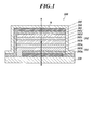
- the schematic diagram which shows an example of a structure of the organic EL element of this invention The schematic diagram which shows an example of the vacuum ultraviolet irradiation apparatus used for formation of the smooth layer based on this invention
- the organic electroluminescent element of the present invention is composed of at least a transparent substrate, a first transparent electrode, an organic light emitting layer, a second transparent electrode and a transparent sealing substrate, and both the transparent substrate and the transparent sealing substrate are
- the first transparent electrode and the second transparent electrode are made of a material selected from the same material group that is flexible and is selected from the same material group. It is characterized by. This feature is a technical feature common to the inventions according to claims 1 to 8.
- the first transparent electrode and the second transparent electrode are both electrodes containing silver or an alloy containing silver as a main component. Since it can be adjusted to a thin film that is thinner than conventional transparent electrodes and does not cause cracking when bent, and it does not cause specular reflection on metal electrodes, it reduces the viewing angle dependency of chromaticity. Moreover, the light emission luminance on both sides can be set arbitrarily, which is preferable.
- a transparent functional layer containing an organic or inorganic compound between the transparent substrate and the first transparent electrode and between the second transparent electrode and the transparent sealing substrate.
- At least one layer of the transparent functional layer is an underlayer containing an organic compound having at least one atom selected from a nitrogen atom and a sulfur atom, and silver or silver forming an electrode as a main component
- an organic compound having at least one atom selected from a nitrogen atom and a sulfur atom, and silver or silver forming an electrode as a main component This is a preferred embodiment in that the aggregation of the alloy is suppressed and the electrode layer can be formed into a thin film, and a more transparent electrode is obtained.
- At least 1 layer of the said transparent functional layer is an electrode protective layer from a viewpoint of reinforcement
- the layer thicknesses of the first transparent electrode and the second transparent electrode are preferably in the range of 5 to 30 nm, respectively, from the viewpoint of obtaining a transparent, thin, and flexible electrode. Moreover, by changing the layer thickness of the first transparent electrode and the second transparent electrode, it is possible to arbitrarily set the light emission luminance on both sides, which is preferable.
- the first transparent electrode, the organic light emitting layer, and the second transparent electrode, which are disposed on the transparent substrate, are laminated and sealed with the transparent sealing base material, thereby forming a hollow portion.
- a double-sided light emitting organic electroluminescence device is obtained in which the reflection at the interface between the electrode and the sealing space is eliminated and the viewing angle dependency of chromaticity is small.
- the ratio a: b is 3 : Within the range of 5 to 5: 3, even if the thickness of the organic light emitting layer is shifted in the design process, the light emission characteristics of both surfaces can be made uniform, and the viewing angle dependency of chromaticity can be further improved. From the viewpoint of reducing the size, it is preferable.
- the organic EL device of the present invention is an organic EL device comprising at least a transparent substrate, a first transparent electrode, an organic light emitting layer, a second transparent electrode, and a transparent sealing substrate, and the transparent substrate and the transparent sealing
- the base material is flexible and is made of a material selected from the same material group, and the first transparent electrode and the second transparent electrode are selected from the same material group.
- the transparent substrate and the transparent sealing substrate are both characterized by flexibility.
- the term “flexibility” as used herein refers to winding a substrate or substrate around a ⁇ (diameter) 50 mm roll. It means that no cracks occur before and after winding with a constant tension.
- “transparent” means that the substrate, base material, electrode, and light emitting layer are respectively transmitted through a light at a light wavelength of 550 nm using a spectrophotometer (U-3300 manufactured by Hitachi High-Technologies Corporation). When the rate (%) is measured, it means having a light transmittance of 50% or more.
- the light transmittance of each element constituting the organic EL element is preferably 60% or more, more preferably 70% or more, and particularly preferably 80% or more.
- the organic EL device of the present invention is a double-sided light emitting type, and in order to meet the demand for the design, the light transmittance of the entire organic EL device at a light wavelength of 550 nm is preferably 50% or more.
- the light transmittance is preferably 60% or more.
- the organic EL element of the present invention can take various configurations, and an example is shown in FIG. However, the present invention is not limited to this.
- FIG. 1 illustrates a case where a resin substrate is used as a substrate used for an organic EL element.
- the organic EL element 100 of the present invention is provided on a transparent substrate 110, and in order from the transparent substrate 110 side, an organic light emitting layer 103 composed of at least a first transparent electrode 101, an organic material, and the like, a second transparent An electrode (counter electrode) 102 and a transparent sealing substrate 105 are laminated in this order.
- the end of the first transparent electrode 101 (electrode layer 101b) has the shape of an extraction electrode, and the first transparent electrode 101 and an external power source (not shown) are electrically connected via the extraction electrode. .
- the organic EL element 100 is configured so that the generated light (emitted light h) is extracted from the transparent substrate 110 side and the transparent sealing substrate 105 side.
- the organic EL element 100 of the present invention is composed of at least a transparent substrate, a first transparent electrode, an organic light emitting layer, a second transparent electrode, and a transparent sealing substrate, both of which are the transparent substrate and the transparent sealing substrate.
- the first transparent electrode and the second transparent electrode are made of a material selected from the same material group that is flexible and is selected from the same material group. is required.
- the transparent substrate and the transparent sealing substrate, and the first transparent electrode and the second transparent electrode are the main components, respectively. It means that it is made of a material selected from the same material group described later.
- the “main component” is 80% by mass or more, more preferably 90% by mass or more as a component of the material constituting the transparent substrate, the transparent sealing substrate, and the first transparent electrode and the second transparent electrode. The component which occupies.
- the layer structure of the organic EL element 100 is not limited, and may be a general layer structure.
- the first transparent electrode 101 functions as an anode (that is, an anode)
- the second transparent electrode 102 functions as a cathode (that is, a cathode).
- the organic light emitting layer 103 is formed by laminating a hole injection layer 103a / a hole transport layer 103b / a light emission layer 103c / an electron transport layer 103d / an electron injection layer 103e in this order from the first transparent electrode 101 side which is an anode.
- the structure is illustrated, it is essential to have the light emitting layer 103c formed using at least an organic material.
- the hole injection layer 103a and the hole transport layer 103b may be provided as a hole transport injection layer.
- the electron transport layer 103d and the electron injection layer 103e may be provided as an electron transport injection layer.
- the electron injection layer 103e may be made of an inorganic material.
- the organic light emitting layer 103 may be laminated with a hole blocking layer, an electron blocking layer, or the like as necessary.
- the light emitting layer 103c may have a structure in which each color light emitting layer that generates light emitted in each wavelength region is stacked, and each of these color light emitting layers is stacked via a non-light emitting intermediate layer.
- the intermediate layer may function as a hole blocking layer and an electron blocking layer.
- the second transparent electrode 102 as the cathode may also have a laminated structure as necessary. In such a configuration, only a portion where the organic light emitting layer 103 is sandwiched between the first transparent electrode 101 and the second transparent electrode 102 becomes a light emitting region in the organic EL element 100.
- an auxiliary electrode (not shown) is provided in contact with the electrode layer 101b of the first transparent electrode 101 for the purpose of reducing the resistance of the first transparent electrode 101. Also good.
- the organic EL element 100 having the above-described configuration is sealed by the transparent sealing substrate 105 on the transparent substrate 110 for the purpose of preventing deterioration of the organic light emitting layer 103 formed using an organic material or the like. ing.
- the transparent sealing substrate 105 is fixed to the transparent substrate 110 side via an adhesive layer on the surface.
- the extraction electrode portion of the first transparent electrode 101 and the terminal portion of the second transparent electrode 102 were exposed from the transparent sealing substrate 105 in a state where the organic light emitting layer 103 maintained insulation from each other on the transparent substrate 110. It is assumed that it is provided in a state.
- the transparent substrate 110 and the transparent sealing substrate 105 preferably have a gas barrier layer in order to protect the organic light emitting layer 103 from the humidity of the external environment.
- the ratio a: b is 3 : 5 to 5: 3 is preferable in order to easily adjust the light emission balance on both sides. Within this range, even when the light emission center moves due to the thickness of the organic light emitting layer being shifted by design, the difference in light emission characteristics between both surfaces is small.
- the ratio a: b is more preferably in the range of 2: 3 to 3: 2.
- the distance a is a distance from the surface of the first transparent electrode on the organic light emitting layer side to the light emission center of the organic light emitting layer (usually the center of the light emitting layer), and the distance b is the second transparent electrode. The distance from the surface on the organic light emitting layer side to the light emission center of the organic light emitting layer (usually the center of the light emitting layer).
- Method for producing organic EL element In the method for producing an organic EL device of the present invention, it is preferable to laminate at least a first transparent electrode, an organic light emitting layer and a second transparent electrode on a transparent substrate, and further laminate and seal with a transparent sealing substrate.
- ⁇ Lamination process> In the method for producing an organic EL element of the present invention, at least a first transparent electrode 101, an organic light emitting layer 103, and a second transparent electrode 102 are laminated on a transparent substrate 110 and further laminated with a transparent sealing substrate 105.
- a transparent functional layer containing an organic or inorganic compound between the transparent substrate and the first transparent electrode and between the second transparent electrode and the transparent sealing substrate.
- a transparent substrate 110 is prepared.
- a base layer 101a made of a nitrogen-containing compound containing nitrogen atoms as a transparent functional layer is formed with a layer thickness of 1 ⁇ m or less, preferably in the range of 10 to 100 nm. It forms by appropriate methods, such as a vapor deposition method.
- the electrode layer 101b made of silver or an alloy containing silver as a main component is formed on the base layer 101a by an appropriate method such as vapor deposition so that the layer thickness is 30 nm or less, preferably in the range of 5 to 30 nm.
- the first transparent electrode 101 is formed to be an anode.
- an extraction electrode portion connected to an external power source is formed at the end of the first transparent electrode 101 by an appropriate method such as a vapor deposition method.
- a hole injection layer 103a, a hole transport layer 103b, a light emitting layer 103c, an electron transport layer 103d, and an electron injection layer 103e are stacked in this order on this, thereby forming the organic light emitting layer 103.
- each of these layers includes spin coating, casting, ink jet, vacuum deposition, and printing, but it is easy to obtain a homogeneous layer and is difficult to produce pinholes. Vapor deposition or spin coating is particularly preferred. Furthermore, different formation methods may be applied for each layer. When a vacuum deposition method is employed for forming each of these layers, the deposition conditions vary depending on the type of compound used, but generally a resistance heating boat is used and the boat heating temperature is 50 to 450 ° C., and the degree of vacuum is 1 ⁇ 10 ⁇ 6.
- the second transparent electrode 102 serving as a cathode is formed on the upper portion by an appropriate forming method such as a vapor deposition method or a sputtering method. At this time, the second transparent electrode 102 is patterned in a shape in which a terminal portion is drawn from the upper side of the organic light emitting layer 103 to the periphery of the transparent substrate 110 while being kept insulated from the first transparent electrode 101 by the organic light emitting layer 103. Form.
- the electrode protective layer 104 is formed as the transparent functional layer according to the present invention.
- the electrode protective layer is preferably formed by an appropriate method such as the coating method or the vapor deposition method so that the layer thickness is 1 ⁇ m or less, preferably in the range of 10 to 100 nm.
- the transparent sealing substrate 105 provided with the adhesive layer is covered on the electrode protective layer 104 and the transparent substrate so as to cover the first transparent electrode, the organic light emitting layer and the second transparent electrode by a method such as thermocompression bonding.
- the organic EL element 100 is manufactured by laminating and sealing on 110.
- the transparent substrate and the transparent sealing substrate according to the present invention are both flexible and are made of a material selected from the same material group.
- a material selected from the same material group means that a material selected from the following material group is used as the resin base material.
- the transparent substrate and the transparent sealing substrate are made of the same material. Moreover, it is advantageous in terms of production cost if they are made of the same material.
- the transparent substrate 110 is basically composed of a transparent resin base material as a support, and one or more gas barrier layers having a refractive index in the range of 1.4 to 1.7 as measured at a light wavelength of 550 nm. It is preferable to be configured. In this case, it is preferable to use the same material for forming the gas barrier layer.
- Resin substrate The resin substrate used in the present invention is a transparent and flexible resin substrate.
- the resin substrate preferably used in the present invention preferably has gas barrier properties such as moisture resistance / gas permeability resistance required for the organic EL element.
- the light transmittance at a light wavelength of 550 nm of the resin substrate is preferably 70% or more, more preferably 80% or more, and further preferably 90% or more.
- the material group constituting the transparent resin base material includes acrylic resins such as acrylic ester, methacrylic ester and PMMA, polyethylene terephthalate (PET), polybutylene terephthalate, polyethylene naphthalate (PEN), polycarbonate ( PC), polyarylate, polyvinyl chloride (PVC), polyethylene (PE), polypropylene (PP), polystyrene (PS), nylon (Ny), aromatic polyamide, polyether ether ketone, polysulfone, polyether sulfonate, polyimide, Basic skeleton of each resin film such as polyetherimide, polyolefin, and epoxy resin, each cycloolefin and cellulose ester resin film, and silsesquioxane having organic-inorganic hybrid structure And heat the transparent film (product name Sila-DEC, manufactured by Chisso Corporation), and further refers to a resin film or the like formed by laminating the resin material 2 or more layers.
- acrylic resins such as acrylic ester,
- polyethylene terephthalate (PET), polyethylene naphthalate (PEN), polycarbonate (PC), acrylic resin, and the like are preferably used from the viewpoint of cost and availability.
- a biaxially stretched polyethylene terephthalate (PET) film and a biaxially stretched polyethylene naphthalate (PEN) film are preferred in terms of transparency, heat resistance, ease of handling, strength, and cost.
- a low heat recovery treatment product that has been subjected to treatment such as thermal annealing is most preferable.
- the thickness of the resin substrate is preferably in the range of 10 to 500 ⁇ m, more preferably in the range of 20 to 250 ⁇ m, and still more preferably in the range of 30 to 150 ⁇ m.
- the thickness of the resin base material is in the range of 10 to 500 ⁇ m, a stable gas barrier property can be obtained, and the resin base material is suitable for conveyance in a roll-to-roll system.
- the resin substrate of the transparent substrate 110 has a refractive index of 1.4 to 1.7 as a transparent functional layer as measured at a light wavelength of 550 nm. It is preferable that one or more gas barrier layers within the range are provided.
- a gas barrier layer a known material can be used without particular limitation, and a film made of an inorganic material or an organic material, or a hybrid film obtained by combining these films may be used.
- the gas barrier layer has a water vapor permeability (25 ⁇ 0.5 ° C., relative humidity 90 ⁇ 2% environment) measured by a method according to JIS K 7129: 1992, 0.01 g / (m 2 ⁇ 24 hours. )
- the following gas barrier film also referred to as a gas barrier film or the like
- the oxygen permeability measured by a method according to JIS K 7126: 1987 is 1 ⁇ 10 ⁇ 3 ml / (m 2 More preferably, it is a high gas barrier film having a water vapor permeability of 1 ⁇ 10 ⁇ 5 g / (m 2 ⁇ 24 hours) or less.
- any material may be used as long as it has a function of suppressing intrusion of elements that cause deterioration of elements such as moisture and oxygen.
- silicon oxide, silicon dioxide, silicon nitride, or the like is used. Can do.
- a structure (organic layer) made of an organic material as a stress relaxation layer may be laminated on these inorganic layers.
- the method for forming the gas barrier layer is not particularly limited.
- the vacuum deposition method, sputtering method, reactive sputtering method, molecular beam epitaxy method, cluster ion beam method, ion plating method, plasma polymerization method, atmospheric pressure plasma weight A combination method, a plasma CVD method, a laser CVD method, a thermal CVD method, a coating method and the like can be used, but an atmospheric pressure plasma polymerization method described in JP-A-2004-68143 is preferable.
- a gas barrier layer is formed by apply
- the inorganic precursor compound used in the present invention is not particularly limited as long as it is a compound capable of forming a metal oxide, a metal nitride, or a metal oxynitride by vacuum ultraviolet irradiation under a specific atmosphere, but is suitable for the present invention.
- the compound is preferably a compound that can be modified at a relatively low temperature as described in JP-A-8-112879.
- polysiloxane including polysilsesquioxane
- polysilazane having Si—N—Si bond
- Si—O—Si bond Si—Si bond
- Si— Polysiloxazan and the like containing both N—Si bonds can be raised. These can be used in combination of two or more. Moreover, it can be used even if different compounds are sequentially laminated or simultaneously laminated.
- polysilazane is preferable, and the polysilazane used in the present invention is a polymer having a silicon-nitrogen bond, and is composed of Si—N, Si—H, NH, or the like, SiO 2 , Si 3 N 4 and the intermediate of both.
- An inorganic precursor polymer such as a solid solution SiO x N y (x: 0.1 to 1.9, y: 0.1 to 1.3).
- the polysilazane preferably used in the present invention is represented by the following general formula (A).
- R 1 , R 2 and R 3 each represent a hydrogen atom, an alkyl group, an alkenyl group, a cycloalkyl group, an aryl group, an alkylsilyl group, an alkylamino group or an alkoxy group.
- perhydropolysilazane in which all of R 1, R 2 and R 3 are hydrogen atoms is particularly preferred from the viewpoint of compactness.
- Polysilazane is commercially available in the form of a solution dissolved in an organic solvent, and the commercially available product can be used as a polysilazane-containing coating solution as it is.
- Examples of commercially available polysilazane solutions include NN120-20, NAX120-20, and NL120-20 manufactured by AZ Electronic Materials Co., Ltd.
- the coating solution containing the polysilazane can be applied and dried, and then subjected to a modification treatment by irradiation with vacuum ultraviolet rays.
- organic solvent for preparing a coating liquid containing polysilazane, it is preferable to avoid using an alcohol or water-containing one that easily reacts with polysilazane.
- organic solvents include hydrocarbon solvents such as aliphatic hydrocarbons, alicyclic hydrocarbons, and aromatic hydrocarbons, ethers such as halogenated hydrocarbon solvents, aliphatic ethers, and alicyclic ethers.
- organic solvents such as pentane, hexane, cyclohexane, toluene, xylene, solvesso and turben, halogen hydrocarbons such as methylene chloride and trichloroethane, and ethers such as dibutyl ether, dioxane and tetrahydrofuran.
- organic solvents may be selected according to purposes such as the solubility of polysilazane and the evaporation rate of the organic solvent, and a plurality of organic solvents may be mixed.
- the concentration of polysilazane in the coating solution for forming a gas barrier layer containing polysilazane varies depending on the layer thickness of the gas barrier layer and the pot life of the coating solution, but is preferably in the range of 0.2 to 35% by mass.
- an amine catalyst In order to promote modification to silicon oxynitride, an amine catalyst, a Pt compound such as Pt acetylacetonate, a Pd compound such as propionic acid Pd, an Rh compound such as Rh acetylacetonate, etc. It is also possible to add a metal catalyst. In the present invention, it is particularly preferable to use an amine catalyst.
- Specific amine catalysts include N, N-diethylethanolamine, N, N-dimethylethanolamine, triethanolamine, triethylamine, 3-morpholinopropylamine, N, N, N ′, N′-tetramethyl-1 , 3-diaminopropane, N, N, N ′, N′-tetramethyl-1,6-diaminohexane and the like.
- the amount of these catalysts added to the polysilazane is preferably in the range of 0.1 to 10% by mass, preferably in the range of 0.2 to 5% by mass, with respect to the total mass of the coating liquid for forming the gas barrier layer. Is more preferable, and it is still more preferable to be in the range of 0.5 to 2% by mass.
- any appropriate wet coating method can be adopted as a method of applying the gas barrier layer forming coating solution containing polysilazane.
- Specific examples include a roller coating method, a flow coating method, an ink jet method, a spray coating method, a printing method, a dip coating method, a casting film forming method, a bar coating method, and a gravure printing method.
- the thickness of the coating film can be appropriately set according to the purpose.
- the thickness of the coating film is preferably in the range of 50 nm to 2 ⁇ m as the thickness after drying, more preferably in the range of 70 nm to 1.5 ⁇ m, and in the range of 100 nm to 1 ⁇ m. Is more preferable.
- the gas barrier layer is a step of irradiating a layer containing polysilazane with vacuum ultraviolet (VUV), and at least a part of the polysilazane is modified into silicon oxynitride.
- VUV vacuum ultraviolet
- perhydropolysilazane will be described as an example of the presumed mechanism in which the coating film containing polysilazane is modified in the vacuum ultraviolet irradiation step and becomes a specific composition of SiO x N y .
- x and y are basically in the range of 2x + 3y ⁇ 4.
- the coating film contains silanol groups, and there are cases where 2 ⁇ x ⁇ 2.5.
- Si—H bonds and N—H bonds in perhydropolysilazane are relatively easily cleaved by excitation with vacuum ultraviolet irradiation and the like. It is considered that they are recombined as N (a dangling bond of Si may be formed). That is, the cured as SiN y composition without oxidizing. In this case, the polymer main chain is not broken. The breaking of Si—H bonds and N—H bonds is promoted by the presence of a catalyst and heating. The cut H is released out of the membrane as H 2 .
- Si—O—Si Bonds by Hydrolysis and Dehydration Condensation Si—N bonds in perhydropolysilazane are hydrolyzed by water, and the polymer main chain is cleaved to form Si—OH.
- Two Si—OH are dehydrated and condensed to form a Si—O—Si bond and harden. This is a reaction that occurs even in the atmosphere, but during vacuum ultraviolet irradiation in an inert atmosphere, it is considered that water vapor generated as outgas from the resin base material by the heat of irradiation becomes the main moisture source.
- Si—OH that cannot be dehydrated and condensed remains, and a cured film having a low gas barrier property represented by a composition of SiO 2.1 to SiO 2.3 is obtained.
- Adjustment of the composition of silicon oxynitride in the layer obtained by subjecting the polysilazane-containing layer to vacuum ultraviolet irradiation can be performed by appropriately controlling the oxidation state by appropriately combining the oxidation mechanisms (1) to (4) described above. .
- ⁇ Vacuum ultraviolet irradiation device with excimer lamp> As a preferable ultraviolet irradiation apparatus for modifying polysilazane, a rare gas excimer lamp that emits vacuum ultraviolet rays of 100 to 230 nm is specifically mentioned.
- Noble gas atoms such as Xe, Kr, Ar, Ne, etc. are called inert gases because they are chemically bonded and do not form molecules.
- rare gas atoms excited atoms
- that have gained energy by discharge or the like can be combined with other atoms to form molecules.
- a feature of the excimer lamp is that the radiation is concentrated on one wavelength, and since only the necessary light is not emitted, the efficiency is high. Moreover, since extra light is not radiated
- a dielectric barrier discharge lamp has a structure in which a discharge is generated between electrodes via a dielectric.
- at least one electrode is disposed between a discharge vessel made of a dielectric and the outside thereof. That's fine.
- a dielectric barrier discharge lamp for example, a rare gas such as xenon is enclosed in a double cylindrical discharge vessel composed of a thick tube and a thin tube made of quartz glass, and a mesh-like second electrode is formed outside the discharge vessel. There is one in which one electrode is provided and another electrode is provided inside the inner tube.
- the dielectric barrier discharge lamp generates a dielectric barrier discharge inside the discharge vessel by applying a high-frequency voltage or the like between the electrodes, and generates excimer light when excimer molecules such as xenon generated by the discharge dissociate.
- Excimer lamps can be lit with low power input because of their high light generation efficiency. In addition, since light having a long wavelength that causes a temperature rise is not emitted and energy is emitted at a single wavelength in the ultraviolet region, the temperature rise of the irradiation object due to the irradiation light itself is suppressed.
- illuminance of the vacuum ultraviolet rays in the coated surface of the polysilazane coating film is subjected is in the range of 30 ⁇ 200mW / cm 2, and more preferably in a range of 50 ⁇ 160mW / cm 2. If it is 30 mW / cm 2 or more, there is no concern about the reduction of the reforming efficiency, and if it is 200 mW / cm 2 or less, the coating film is not ablated and the substrate is not damaged.
- Irradiation energy amount of the VUV in the polysilazane coating film surface is preferably in the range of 200 ⁇ 10000mJ / cm 2, and more preferably in a range of 500 ⁇ 5000mJ / cm 2. If it is 200 mJ / cm 2 or more, the modification can be sufficiently performed, and if it is 10000 mJ / cm 2 or less, it is not over-reformed and cracking and thermal deformation of the resin substrate can be prevented. .
- the first transparent electrode and the second transparent electrode according to the present invention are made of a material selected from the same material group.
- a material selected from the same material group means that a material selected from the following material group is used as an electrode.
- the first transparent electrode and the second transparent electrode are made of the same material.
- Materials that can be used for the first transparent electrode include aluminum, silver, magnesium, lithium, magnesium / same mixture, magnesium / silver mixture, magnesium / aluminum mixture, magnesium / indium mixture, indium, lithium / aluminum mixture, rare earth
- An oxide semiconductor such as metal, ITO, ZnO, TiO 2 , or SnO 2 is used.
- the configuration of the first transparent electrode is, for example, as shown in FIG. 1, in the first transparent electrode 101, a base layer 101a and an electrode layer 101b formed thereon are sequentially laminated from the transparent substrate 110 side.
- a layer structure is preferred.
- the electrode layer 101b is a layer formed using, for example, silver or an alloy containing silver as a main component
- the base layer 101a is, for example, at least one kind of atom selected from a nitrogen atom and a sulfur atom. It is preferable that it is a layer containing the organic compound which has.
- the transparency of the first transparent electrode 101 means that the light transmittance at a light wavelength of 550 nm is 50% or more.
- the main component in the electrode layer 101b means that the content in the electrode layer 101b is 98% by mass or more.
- the base layer 101a is a layer as a transparent functional layer provided on the transparent substrate 110 side of the electrode layer 101b.
- the material constituting the base layer 101a is not particularly limited as long as it can suppress the aggregation of silver when forming the electrode layer 101b made of silver or an alloy containing silver as a main component.
- the organic compound may be one kind or a mixture of two or more kinds. In addition, it is allowed to mix a compound having no nitrogen atom and sulfur atom within a range that does not impair the effect of the underlayer.
- the upper limit of the layer thickness is preferably less than 50 nm, more preferably less than 30 nm, and less than 10 nm. More preferably, the thickness is less than 5 nm. By making the layer thickness less than 50 nm, optical loss can be minimized.
- the lower limit of the layer thickness is preferably 0.05 nm or more, more preferably 0.1 nm or more, and particularly preferably 0.3 nm or more. By setting the layer thickness to 0.05 nm or more, it is possible to make the underlayer 101a uniform, and to make the effect (inhibition of silver aggregation) uniform.
- the upper limit of the layer thickness is not particularly limited, and the lower limit of the layer thickness is the same as that of the low refractive index material. is there.
- the base layer 101a is formed with a necessary layer thickness that enables uniform film formation.
- a wet process such as a coating method, an inkjet method, a coating method, or a dip method, or a dry process such as a vapor deposition method (resistance heating, EB method, etc.), a sputtering method, a CVD method, or the like is used. And the like. Among these, the vapor deposition method is preferably applied.
- the organic compound having a nitrogen atom is preferably a compound having a melting point of 80 ° C. or higher and a molecular weight Mw in the range of 150 to 1200.
- a compound having a large interaction with the alloy is preferable, and examples thereof include a nitrogen-containing heterocyclic compound and a phenyl group-substituted amine compound.
- the organic compound having a nitrogen atom has an effective unshared electron pair content [n / M] (ratio of the number n of effective unshared electron pairs to the molecular weight M of the organic compound having a nitrogen atom) is 2.0 ⁇ .
- the compound is selected to be 10 ⁇ 3 or more, and more preferably 3.9 ⁇ 10 ⁇ 3 or more.
- the effective unshared electron pair is an unshared electron pair that does not participate in aromaticity and is not coordinated to the metal among the unshared electron pairs of the nitrogen atoms constituting the compound. To do.
- the aromaticity here means an unsaturated cyclic structure in which atoms having ⁇ electrons are arranged in a ring, and is aromatic according to the so-called “Hückel rule”, and is included in the ⁇ electron system on the ring. Is 4n + 2 (n is an integer of 0 or more).
- the effective unshared electron pair as described above is such that the unshared electron pair possessed by the nitrogen atom is aromatic regardless of whether or not the nitrogen atom itself provided with the unshared electron pair is a heteroatom constituting the aromatic ring. It is selected based on whether or not it is involved in the family. For example, even if a nitrogen atom is a heteroatom constituting an aromatic ring, if the nitrogen atom has an unshared electron pair that does not participate in aromaticity, the unshared electron pair is an effective unshared electron pair. Counted as one of
- the number n of effective unshared electron pairs coincides with the number of nitrogen atoms having effective unshared electron pairs.
- the effective unshared electron pair content [n / M] is based on the mixing ratio of each compound and the effective molecular weight M of the mixed compound.
- the number n of unshared electron pairs is calculated, and the ratio of the number n of effective unshared electron pairs to the molecular weight M is defined as the effective unshared electron pair content [n / M], and this value is within the predetermined range described above. It is preferable that
- the low molecular weight organic compound having a nitrogen atom constituting the underlayer As the low molecular weight organic compound having a nitrogen atom constituting the underlayer, the above-described exemplary compound No. 1 having an effective unshared electron pair content [n / M] of 2.0 ⁇ 10 ⁇ 3 or more is used. 1 to 45 are shown, but the present invention is not particularly limited thereto.
- Exemplified Compound No. In 31 copper phthalocyanine among the unshared electron pairs of nitrogen atoms, the unshared electron pairs of nitrogen atoms not coordinated to copper are counted as effective unshared electron pairs.
- the above exemplified compound No. Table 1 shows the number n of effective unshared electron pairs, the molecular weight M, and the effective unshared electron pair content [n / M] for 1 to 45.
- polymer having a nitrogen atom in the present invention, a polymer can also be used as the organic compound having a nitrogen atom.
- the polymer having a nitrogen atom preferably has a weight average molecular weight in the range of 1,000 to 1,000,000.
- the polymer having a nitrogen atom is preferably a polymer having a partial structure represented by the following general formula (P1) or a partial structure represented by the following general formula (P2).
- a 1 represents a divalent nitrogen atom-containing group.
- Y 1 represents a divalent organic group or a bond.
- n1 represents the number of repetitions with a weight average molecular weight in the range of 1,000 to 1,000,000.
- a 2 represents a monovalent nitrogen atom-containing group.
- n2 represents an integer of 1 or more.
- n2 is preferably an integer of 1 to 3 from the viewpoint of interaction with silver, and more preferably 1 or 2 from the viewpoint of ease of synthesis.
- the plurality of A 2 may be the same or different.
- a 3 and A 4 represent a divalent nitrogen atom-containing group.
- a 3 and A 4 may be the same or different.
- n3 and n4 each independently represents 0 or 1.
- Y 2 represents an (n2 + 2) valent organic group.
- n1 represents the number of repetitions with a weight average molecular weight in the range of 1,000 to 1,000,000.
- the polymer having the partial structure represented by the general formula (P1) or (P2) is a homopolymer composed of only a single structural unit derived from the general formula (P1) or (P2). It may be a copolymer (copolymer) composed of only two or more structural units derived from the above general formulas (P1) and / or (P2).
- the copolymer may be formed by further having another structural unit having no nitrogen atom-containing group.
- the content of the monomer derived from the other structural unit has the effect of the polymer having a nitrogen atom according to the present invention.
- it is not particularly limited as long as it is not impaired, it is preferably in the range of 10 to 75 mol%, more preferably in the range of 20 to 50 mol% in the monomers derived from all structural units.
- the terminal of the polymer having the partial structure represented by the general formula (P1) or (P2) is not particularly limited and is appropriately defined depending on the type of raw material (monomer) used. is there.
- the monovalent nitrogen atom-containing group represented by A 2 is not particularly limited as long as it is an organic group having a nitrogen atom.
- nitrogen atom-containing groups include amino groups, dithiocarbamate groups, thioamide groups, cyano groups (—CN), isonitrile groups (—N + ⁇ C ⁇ ), isocyanate groups (—N ⁇ C ⁇ O). ), A thioisocyanate group (—N ⁇ C ⁇ S), or a group containing a substituted or unsubstituted nitrogen-containing aromatic ring.
- PN1 to 41 Specific examples (PN1 to 41) of monomers constituting the polymer having a nitrogen atom according to the present invention are shown below, but are not particularly limited thereto.
- the polymer having a nitrogen atom is composed of the following monomers having a number of repetitions in a range where the weight average molecular weight is 1,000 to 1,000,000.
- the low molecular organic compound and polymer having a nitrogen atom according to the present invention can be synthesized by a known and well-known method.
- the organic compound having a sulfur atom according to the present invention has a sulfide bond, disulfide bond, mercapto group, sulfone group, thiocarbonyl bond and the like in the molecule. Among these, it is preferable to have a sulfide bond or a mercapto group.
- the organic compound having a sulfur atom is preferably a compound represented by the following general formulas (1) to (4).
- R 1 and R 2 each independently represent a substituent.
- R 3 and R 4 each independently represent a substituent.
- R 5 represents a substituent
- R 6 represents a substituent
- examples of the substituent represented by R 1 and R 2 include an alkyl group (for example, methyl group, ethyl group, propyl group, isopropyl group, tert-butyl group, pentyl group, hexyl group).
- alkyl group for example, methyl group, ethyl group, propyl group, isopropyl group, tert-butyl group, pentyl group, hexyl group.
- substituents may be further substituted with these substituents, or may be linked to each other to form a ring.
- examples of the substituent represented by R 3 and R 4 include the same substituents as the substituents represented by R 1 and R 2 in the general formula (1).
- examples of the substituent represented by R 5 include the same substituents as the substituents represented by R 1 and R 2 in the general formula (1).
- examples of the substituent represented by R 6 include the same substituents as the substituents represented by R 1 and R 2 in the general formula (1).
- Polymer having a sulfur atom In the present invention, a polymer may be used as the organic compound having a sulfur atom.
- the polymer having a sulfur atom preferably has a weight average molecular weight in the range of 1,000 to 1,000,000.
- PS1 to 14 Specific examples (PS1 to 14) of monomers constituting the polymer having a sulfur atom are shown below, but are not particularly limited thereto.
- the polymer having a sulfur atom is composed of the following monomers having a number of repetitions in a range where the weight average molecular weight is 1,000 to 1,000,000.
- the numerical values added outside the parentheses represent the constituent ratio (also referred to as molar ratio or composition ratio) of each monomer unit.
- Table 2 shows the weight average molecular weight of the polymer composed of the above monomer units.
- the organic compound and polymer having a sulfur atom used in the present invention can be synthesized by a known and well-known method.
- the weight average molecular weight of the polymer which has a nitrogen atom or sulfur atom used for this invention is the value which measured on the following measurement conditions under room temperature (25 degreeC).
- Equipment Tosoh High Speed GPC Equipment HLC-8220GPC Column: TOSOH TSKgel Super HM-M Detector: RI and / or UV Eluent flow rate: 0.6 ml / min Temperature: 30 ° C Sample concentration: 0.1% by mass Sample volume: 100 ⁇ l
- Electrode layer 101b is preferably a layer formed using silver or an alloy containing silver as a main component, and is preferably a layer formed on the base layer 101a.
- a wet process such as a coating method, an inkjet method, a coating method, or a dip method, a vapor deposition method (resistance heating, EB method, etc.), a sputtering method, a CVD method, or the like is used. And a method using the dry process. Among these, the vapor deposition method is preferably applied.
- the electrode layer 101b is formed on the base layer 101a, so that the electrode layer 101b has sufficient conductivity even without high-temperature annealing after the electrode layer 101b is formed.
- the film may be subjected to high-temperature annealing after film formation.
- Examples of the alloy mainly composed of silver (Ag) constituting the electrode layer 101b include silver magnesium (AgMg), silver copper (AgCu), silver palladium (AgPd), silver palladium copper (AgPdCu), and silver indium (AgIn). ) And the like.
- the electrode layer 101b as described above may have a configuration in which silver or an alloy layer mainly composed of silver is divided into a plurality of layers as necessary.
- the electrode layer 101b preferably has a layer thickness in the range of 5 to 30 nm.
- the layer thickness is less than 30 nm, the absorption component or reflection component of the layer is small, and the transmittance of the first transparent electrode 101 is increased.
- the layer thickness is thicker than 5 nm, the conductivity of the layer can be sufficiently secured.
- the range is preferably 8 to 20 nm, and more preferably 10 to 15 nm.
- the light distribution characteristics on the first transparent electrode side and the second transparent electrode side can be freely set while keeping the color shift small. Can be controlled (see, eg, Example 3).
- the first transparent electrode 101 having a laminated structure composed of the base layer 101a and the electrode layer 101b formed thereon is covered with a protective film on the upper part of the electrode layer 101b or another electrode. Layers may be laminated. In this case, it is preferable that the protective film and the other electrode layer have light transmittance so as not to impair the light transmittance of the first transparent electrode 101.
- the first transparent electrode 101 having the above-described configuration is, for example, an underlayer formed using an organic compound having at least one atom selected from a nitrogen atom and a sulfur atom.
- An electrode layer 101b made of silver or an alloy containing silver as a main component is provided on 101a.
- the silver atoms constituting the electrode layer 101b interact with the compound containing nitrogen atoms or sulfur atoms constituting the base layer 101a, so that the silver The diffusion distance of atoms on the surface of the underlying layer 101a is reduced, and aggregation of silver is suppressed.
- the electrode layer 101b containing silver as a main component a thin film is grown in a nucleus growth type (Volume-Weber: VW type), and therefore, silver particles are easily isolated in an island shape, and the layer thickness is increased.
- a nucleus growth type Volume-Weber: VW type
- the layer thickness is increased.
- the thickness is thin, it is difficult to obtain conductivity, and the sheet resistance value becomes high. Therefore, although it is necessary to increase the layer thickness in order to ensure conductivity, it is difficult to use as the first transparent electrode because the light transmittance decreases as the layer thickness increases.
- the electrode layer 101b made of silver or an alloy containing silver as a main component is formed. Is not a nucleus growth type but a single layer growth type (Frank-van der Merwe: FM type).
- the first transparent electrode 101 is preferably a transparent electrode having a light transmittance of 50% or more at a light wavelength of 550 nm, and an electrode layer made of silver or an alloy containing silver as a main component by providing the base layer 101a.
- 101b can be thinned and can be a film with sufficiently good light transmittance.
- the conductivity of the first transparent electrode 101 is mainly ensured by the electrode layer 101b.
- the electrode layer 101b made of silver or an alloy containing silver as a main component has excellent conductivity, and conductivity is ensured with a thinner layer thickness. Accordingly, it is possible to achieve both the improvement of the conductivity of the first transparent electrode 101 and the improvement of the light transmittance.
- the first transparent electrode according to the present invention can be adjusted to a thin film within a range where specular reflection at the silver electrode does not occur, it can contribute to an improvement in light emission luminance.
- Organic light emitting layer 103 includes at least a light emitting layer 103c.
- the phosphor layer 103c used in the present invention preferably contains a phosphorescent compound as a luminescent material.
- a fluorescent material may be used as the light emitting material, or a phosphorescent light emitting compound and a fluorescent material may be used in combination.
- the light emitting layer 103c is a layer that emits light by recombination of electrons injected from the electrode or the electron transport layer 103d and holes injected from the hole transport layer 103b, and the light emitting portion is the light emitting layer 103c. Even within the layer, it may be an interface between the light emitting layer 103c and the adjacent layer.
- the structure of the light emitting layer 103c is not particularly limited as long as the included light emitting material satisfies the light emission requirements. Moreover, there may be a plurality of layers having the same emission spectrum and emission maximum wavelength. In this case, a non-light emitting intermediate layer (not shown) is preferably provided between the light emitting layers 103c.
- the total thickness of the light emitting layer 103c is preferably in the range of 1 to 100 nm, and more preferably in the range of 1 to 30 nm because a lower driving voltage can be obtained.
- the sum of the layer thicknesses of the light emitting layer 103c is a layer thickness including the intermediate layer when a non-light emitting intermediate layer exists between the light emitting layers 103c.
- the thickness of each light emitting layer is preferably adjusted within a range of 1 to 50 nm, and more preferably adjusted within a range of 1 to 20 nm. preferable.
- the plurality of stacked light emitting layers correspond to blue, green, and red light emission colors, there is no particular limitation on the relationship between the thicknesses of the blue, green, and red light emitting layers.
- the light emitting layer 103c as described above is formed by forming a known light emitting material or host compound by a known thin film forming method such as a vacuum deposition method, a spin coating method, a casting method, an LB method, or an ink jet method. be able to.
- a known thin film forming method such as a vacuum deposition method, a spin coating method, a casting method, an LB method, or an ink jet method.
- a light-emitting dopant also referred to as a light-emitting dopant compound
- a host compound contained in the light-emitting layer will be described.
- the host compound means that the compound contained in the light emitting layer has a mass ratio of 20% or more in the layer and is phosphorus at room temperature (25 ° C.).
- a compound having a phosphorescence quantum yield of photoluminescence of less than 0.1 is defined.
- the phosphorescence quantum yield is preferably less than 0.01.
- the mass ratio in the layer is 20% or more among the compounds contained in a light emitting layer.
- known host compounds may be used alone or in combination of two or more.
- the organic EL element can be made highly efficient.
- the light emitting host used in the present invention may be a conventionally known low molecular compound or a high molecular compound having a repeating unit, and a low molecular compound having a polymerizable group such as a vinyl group or an epoxy group (deposition polymerization property). Light emitting host).
- a compound that has a hole transporting ability and an electron transporting ability, prevents the emission of light from becoming longer wavelength, and has a high Tg (glass transition temperature) is preferable.
- the light emitting layer of the organic EL device of the present invention preferably contains a phosphorescent dopant at the same time as containing the host compound.
- the phosphorescent dopant used in the present invention is a compound in which light emission from an excited triplet is observed, specifically phosphorescent light emission at room temperature (25 ° C.). Although it is a compound and a phosphorescence quantum yield is defined as a compound 0.01 or more at 25 degreeC, a preferable phosphorescence quantum yield is 0.1 or more.
- the phosphorescent quantum yield can be measured by the method described in Spectroscopic II, page 398 (1992 edition, Maruzen) of the Fourth Edition Experimental Chemistry Course 7. Although the phosphorescence quantum yield in a solution can be measured using various solvents, the phosphorescence dopant used in the present invention achieves the phosphorescence quantum yield (0.01 or more) in any solvent. Just do it.
- the energy transfer type that obtains light emission from the phosphorescent dopant, and the other is that the phosphorescent dopant becomes a carrier trap, carrier recombination occurs on the phosphorescent dopant, and light emission from the phosphorescent dopant is obtained.
- the excited state energy of the phosphorescent dopant is required to be lower than the excited state energy of the host compound.
- a preferable phosphorescent dopant includes an organometallic complex having Ir as a central metal. More preferably, a complex containing at least one coordination mode among a metal-carbon bond, a metal-nitrogen bond, a metal-oxygen bond, and a metal-sulfur bond is preferable.
- At least one light emitting layer 103c may contain two or more types of phosphorescent compounds, and the concentration ratio of the phosphorescent compounds in the light emitting layer 103c is the thickness of the light emitting layer 103c. It may change in direction.
- the phosphorescent compound is preferably 0.1% by volume or more and less than 30% by volume with respect to the total amount of the light emitting layer 103c.
- Fluorescent compounds include coumarin dyes, pyran dyes, cyanine dyes, croconium dyes, squalium dyes, oxobenzanthracene dyes, fluorescein dyes, rhodamine dyes, Examples include pyrylium dyes, perylene dyes, stilbene dyes, polythiophene dyes, and rare earth complex phosphors.
- injection layer (hole injection layer, electron injection layer)
- the injection layer is a layer provided between the electrode and the light-emitting layer 103c in order to lower the drive voltage and improve the light emission luminance.
- the injection layer can be provided as necessary.
- the hole injection layer 103a may exist between the anode and the light emitting layer 103c or the hole transport layer 103b, and the electron injection layer 103e may exist between the cathode and the light emitting layer 103c or the electron transport layer 103d.
- hole injection layer 103a Details of the hole injection layer 103a are described in JP-A-9-45479, JP-A-9-260062, JP-A-8-288069, and the like.
- Specific examples include phthalocyanine represented by copper phthalocyanine.
- examples thereof include a layer, an oxide layer typified by vanadium oxide, an amorphous carbon layer, and a polymer layer using a conductive polymer such as polyaniline (emeraldine) or polythiophene.
- the details of the electron injection layer 103e are described in JP-A-6-325871, JP-A-9-17574, JP-A-10-74586, and the like, and specifically represented by strontium, aluminum and the like. Examples thereof include a metal layer, an alkali metal halide layer typified by potassium fluoride, an alkaline earth metal compound layer typified by magnesium fluoride, and an oxide layer typified by molybdenum oxide.
- the electron injection layer 103e used in the present invention is desirably a very thin film, and the layer thickness is preferably in the range of 1 nm to 10 ⁇ m although it depends on the material.
- the hole transport layer 103b is made of a hole transport material having a function of transporting holes, and in a broad sense, the hole injection layer 103a and the electron blocking layer are also included in the hole transport layer 103b. .
- the hole-transport layer 103b can be provided as a single layer or a plurality of layers.
- the hole transport material has any of hole injection or transport and electron barrier properties, and may be either organic or inorganic.
- triazole derivatives oxadiazole derivatives, imidazole derivatives, polyarylalkane derivatives, pyrazoline derivatives and pyrazolone derivatives, phenylenediamine derivatives, arylamine derivatives, amino-substituted chalcone derivatives, oxazole derivatives, styrylanthracene derivatives, fluorenone derivatives, hydrazone derivatives
- Examples thereof include stilbene derivatives, silazane derivatives, aniline copolymers, and conductive polymer oligomers, particularly thiophene oligomers.
- hole transport material those described above can be used, but it is preferable to use a porphyrin compound, an aromatic tertiary amine compound and a styrylamine compound, particularly an aromatic tertiary amine compound.
- aromatic tertiary amine compounds and styrylamine compounds include N, N, N ′, N′-tetraphenyl-4,4′-diaminophenyl; N, N′-diphenyl-N, N′— Bis (3-methylphenyl)-[1,1′-biphenyl] -4,4′-diamine (TPD); 2,2-bis (4-di-p-tolylaminophenyl) propane; 1,1-bis (4-di-p-tolylaminophenyl) cyclohexane; N, N, N ′, N′-tetra-p-tolyl-4,4′-diaminobiphenyl; 1,1-bis (4-di-p-tolyl) Aminophenyl) -4-phenylcyclohexane; bis (4-dimethylamino-2-methylphenyl) phenylmethane; bis (4-di-p-tolylaminoph
- a polymer material in which these materials are introduced into a polymer chain or these materials are used as a polymer main chain can also be used.
- inorganic compounds such as p-type-Si and p-type-SiC can also be used as the hole injection material and the hole transport material.
- a so-called p-type hole transport material as described in 139 can also be used. In the present invention, it is preferable to use these materials because a light-emitting element with higher efficiency can be obtained.
- the hole transport layer 103b is formed by thinning the hole transport material by a known method such as a vacuum deposition method, a spin coating method, a casting method, a printing method including an inkjet method, or an LB method. be able to.
- the layer thickness of the hole transport layer 103b is not particularly limited, but is usually about 5 nm to 5 ⁇ m, preferably 5 to 200 nm.
- the hole transport layer 103b may have a single layer structure composed of one or more of the above materials.
- Examples thereof include JP-A-4-297076, JP-A-2000-196140, 2001-102175, J.A. Appl. Phys. 95, 5773 (2004), and the like.
- the electron transport layer 103d is made of a material having a function of transporting electrons. In a broad sense, the electron injection layer 103e and a hole blocking layer (not shown) are also included in the electron transport layer 103d.
- the electron transport layer 103d can be provided as a single-layer structure or a stacked structure of a plurality of layers.
- an electron transport material (also serving as a hole blocking material) constituting a layer portion adjacent to the light emitting layer 103c was injected from the cathode. What is necessary is just to have the function to transmit an electron to the light emitting layer 103c.
- any one of conventionally known compounds can be selected and used.
- Examples include nitro-substituted fluorene derivatives, diphenylquinone derivatives, thiopyran dioxide derivatives, carbodiimides, fluorenylidenemethane derivatives, anthraquinodimethane, anthrone derivatives, and oxadiazole derivatives.
- a thiadiazole derivative in which the oxygen atom of the oxadiazole ring is substituted with a sulfur atom, and a quinoxaline derivative having a quinoxaline ring known as an electron-withdrawing group are also used as the material for the electron transport layer 103d.
- a polymer material in which these materials are introduced into a polymer chain or these materials are used as a polymer main chain can also be used.
- metal complexes of 8-quinolinol derivatives such as tris (8-quinolinol) aluminum (Alq 3 ), tris (5,7-dichloro-8-quinolinol) aluminum, tris (5,7-dibromo-8-quinolinol) Aluminum, tris (2-methyl-8-quinolinol) aluminum, tris (5-methyl-8-quinolinol) aluminum, bis (8-quinolinol) zinc (Znq), etc.
- Mg Metal complexes replaced with Cu, Ca, Sn, Ga, or Pb can also be used as the material for the electron transport layer 103d.
- metal-free or metal phthalocyanine or those having terminal ends substituted with an alkyl group or a sulfonic acid group can be preferably used as the material for the electron transport layer 103d.
- a distyrylpyrazine derivative exemplified also as a material of the light-emitting layer 103c can be used as a material of the electron-transport layer 103d, and n-type Si, n-type similarly to the hole-injection layer 103a and the hole-transport layer 103b.
- An inorganic semiconductor such as type-SiC can also be used as the material of the electron transport layer 103d.
- the electron transport layer 103d can be formed by thinning the above material by a known method such as a vacuum deposition method, a spin coating method, a casting method, a printing method including an ink jet method, or an LB method.
- the layer thickness of the electron transport layer 103d is not particularly limited, but is usually about 5 nm to 5 ⁇ m, preferably 5 to 200 nm.
- the electron transport layer 103d may have a single-layer structure made of one or more of the above materials.
- the electron transport layer 103d can be doped with an impurity to increase the n property.
- examples thereof include JP-A-4-297076, JP-A-10-270172, JP-A-2000-196140, 2001-102175, J.A. Appl. Phys. 95, 5773 (2004), and the like.
- the electron transport layer 103d contains potassium, a potassium compound, or the like.
- the potassium compound for example, potassium fluoride can be used.
- the material (electron transporting compound) of the electron transport layer 103d the same material as that of the base layer 101a described above may be used.
- the electron transport layer 103d that also serves as the electron injection layer 103e the same material as that of the base layer 101a described above may be used.
- Blocking layer (hole blocking layer, electron blocking layer)
- the blocking layer may be further provided as the organic light emitting layer 103 in addition to the above functional layers. For example, it is described in JP-A Nos. 11-204258 and 11-204359, and “Organic EL elements and the forefront of industrialization (published by NTT Corporation on November 30, 1998)” on page 237. There is a hole blocking (hole blocking) layer.
- the hole blocking layer has a function of the electron transport layer 103d in a broad sense.
- the hole blocking layer is made of a hole blocking material that has a function of transporting electrons but has a very small ability to transport holes, and recombines electrons and holes by blocking holes while transporting electrons. Probability can be improved.
- the structure of the electron carrying layer 103d mentioned later can be used as a hole-blocking layer used for this invention as needed.
- the hole blocking layer is preferably provided adjacent to the light emitting layer 103c.
- the electron blocking layer has a function of the hole transport layer 103b in a broad sense.
- the electron blocking layer is made of a material that has a function of transporting holes and has an extremely small ability to transport electrons, By blocking electrons while transporting holes, the probability of recombination of electrons and holes can be improved. Further, the structure of the hole transport layer 103b can be used as an electron blocking layer as necessary.
- the layer thickness of the hole blocking layer used in the present invention is preferably in the range of 3 to 100 nm, more preferably in the range of 5 to 30 nm.
- Film formation of each of the hole injection layer 103a, the hole transport layer 103b, the light emitting layer 103c, the electron transport layer 103d, and the electron injection layer 103e described above is performed by a spin coating method, a casting method, an ink jet method, an evaporation method, and a printing method.
- the vacuum deposition method or the spin coating method is particularly preferable from the viewpoints that a homogeneous film is easily obtained and pinholes are hardly generated.
- different film formation methods may be applied for each layer.
- the vapor deposition conditions vary depending on the type of compound used, but generally the boat heating temperature is in the range of 50 to 450 ° C.
- each condition is selected as appropriate within a range of ⁇ 2 Pa, a deposition rate of 0.01 to 50 nm / second, a substrate temperature of ⁇ 50 to 300 ° C., and a layer thickness of 0.1 to 5 ⁇ m.
- the second transparent electrode 102 is an electrode film that functions as a cathode for supplying electrons to the organic light emitting layer 103, and a metal, an alloy, an organic or inorganic conductive compound, and a mixture thereof are used.
- the first transparent electrode and the second transparent electrode according to the present invention are made of a material selected from the same material group.
- a material selected from the same material group means that a material selected from the following material group is used as an electrode.
- the first transparent electrode and the second transparent electrode are made of the same material.
- Materials that can be used for the second transparent electrode include aluminum, silver, magnesium, lithium, magnesium / same mixture, magnesium / silver mixture, magnesium / aluminum mixture, magnesium / indium mixture, indium, lithium / aluminum mixture, rare earth
- An oxide semiconductor such as metal, ITO, ZnO, TiO 2 , or SnO 2 is used.
- the second transparent electrode 102 is preferably a layer composed of silver or an alloy containing silver as a main component.
- a method for forming such an electrode layer of the second transparent electrode 102 As a method for forming such an electrode layer of the second transparent electrode 102, a method using a wet process such as a coating method, an ink jet method, a coating method, a dip method, a vapor deposition method (resistance heating, EB method, etc.), sputtering, etc. And a method using a dry process such as a CVD method. Among these, the vapor deposition method is preferably applied.
- Examples of the alloy mainly composed of silver (Ag) constituting the electrode layer include silver magnesium (AgMg), silver copper (AgCu), silver palladium (AgPd), silver palladium copper (AgPdCu), and silver indium (AgIn). ) And the like.
- the electrode layer as described above may have a configuration in which silver or an alloy layer mainly composed of silver is divided into a plurality of layers as necessary.
- the electrode layer preferably has a layer thickness in the range of 5 to 30 nm.
- the layer thickness is less than 30 nm, the absorption component or reflection component of the layer is small, and the transmittance of the second transparent electrode 102 is increased.
- the layer thickness is thicker than 5 nm, the conductivity of the layer can be sufficiently secured.
- the range is preferably 8 to 20 nm, and more preferably 10 to 15 nm.
- the layer thickness of the metal layer of the first transparent electrode and the second transparent electrode by appropriately changing the layer thickness of the metal layer of the first transparent electrode and the second transparent electrode, the light distribution characteristics on the first transparent electrode side and the second transparent electrode side can be maintained while keeping the color shift small. It can be controlled freely.
- the extraction electrode is for electrically connecting the first transparent electrode 101 and the second transparent electrode 102 and an external power source, and the material thereof is not particularly limited, and a known material can be suitably used.
- a metal film such as a MAM electrode (Mo / Al ⁇ Nd alloy / Mo) having a three-layer structure can be used.
- the auxiliary electrode is provided for the purpose of reducing the resistance of the first transparent electrode 101 and the second transparent electrode 102, and is provided in contact with the electrode layer 101 b of the first transparent electrode 101 and the electrode layer of the second transparent electrode 102.
- the material for forming the auxiliary electrode is preferably a metal having low resistance such as gold, platinum, silver, copper, or aluminum. Since these metals have low light transmittance, a pattern is formed in a range not affected by extraction of the emitted light h from the light extraction surface.
- auxiliary electrodes examples include vapor deposition, sputtering, printing, ink jet, and aerosol jet.
- the line width of the auxiliary electrode is preferably 50 ⁇ m or less from the viewpoint of the aperture ratio for extracting light, and the thickness of the auxiliary electrode is preferably 1 ⁇ m or more from the viewpoint of conductivity.
- Electrode protective layer As at least one layer of the transparent functional layer according to the present invention, forming an electrode protective layer 104 containing an organic or inorganic compound between the second transparent electrode 102 and the transparent sealing substrate 105, This is preferable in order to smooth the surface of the second transparent electrode and to provide sufficient mechanical protection. Moreover, when laminating a transparent sealing base material, since it is solid-sealed, adhesive strength is high.
- the electrode protective layer 104 as described above preferably has flexibility, and a thin polymer film or a thin metal film can be used.
- the organic compound used in the base layer or the organic light emitting layer can be used. It is also preferable that the layer is appropriately selected and formed by the coating method or the vapor deposition method.
- the preferred layer thickness can be appropriately set depending on the purpose, but is preferably about 10 nm to 10 ⁇ m, more preferably about 15 nm to 1 ⁇ m, and further preferably in the range of 20 to 500 nm. .
- the transparent sealing substrate 105 is made of a material that is flexible and selected from the same material group as that of the transparent substrate 110, and has a function of laminating the organic EL element 100 as a function. As shown in the illustrated example, it is fixed to the electrode protective layer 104 side and the transparent substrate 110 side by, for example, an adhesive layer (not shown) containing an adhesive. Such a transparent sealing substrate 105 is provided in a state in which the terminal portions of the first transparent electrode 101 and the second transparent electrode 102 in the organic EL element 100 are exposed and at least the organic light emitting layer 103 is completely covered.
- the transparent substrate 110 and the transparent sealing base material 105 according to the present invention are both flexible and made of a material selected from the same material group.
- a material selected from the same material group means using a material selected from the following material group as a resin base material, and using a material selected from the same material group as the transparent substrate 110.
- the transparent substrate and the transparent sealing substrate are made of the same material.
- the transparent sealing substrate 105 basically includes a transparent resin substrate as a support and one or more gas barrier layers having a refractive index of 1.4 to 1.7 in a light wavelength measurement of 550 nm. It is preferable that it is comprised by these. In this case, it is preferable to use the same material for forming the gas barrier layer.
- Resin base material The resin base material used in the present invention is transparent and is a flexible resin base material.
- the resin substrate preferably used in the present invention preferably has gas barrier properties such as moisture resistance / gas permeability resistance required for the organic EL element.
- the light transmittance at a light wavelength of 550 nm of the resin substrate is preferably 70% or more, more preferably 80% or more, and further preferably 90% or more.
- the material group constituting the transparent resin base material includes acrylic resins such as acrylic ester, methacrylic ester and PMMA, polyethylene terephthalate (PET), polybutylene terephthalate, polyethylene naphthalate (PEN), polycarbonate ( PC), polyarylate, polyvinyl chloride (PVC), polyethylene (PE), polypropylene (PP), polystyrene (PS), nylon (Ny), aromatic polyamide, polyether ether ketone, polysulfone, polyether sulfonate, polyimide, Each resin film such as polyetherimide, polyolefin, and epoxy resin, cycloolefin-based and cellulose ester-based resin films, and silsesquioxane having an organic-inorganic hybrid structure as a basic skeleton Heat transparent film (product name Sila-DEC, manufactured by Chisso Corporation), and further refers to a resin film or the like formed by laminating the resin material 2 or more layers.
- acrylic resins such as
- polyethylene terephthalate (PET), polyethylene naphthalate (PEN), polycarbonate (PC), acrylic resin, and the like are preferably used from the viewpoint of cost and availability.
- a biaxially stretched polyethylene terephthalate (PET) film and a biaxially stretched polyethylene naphthalate (PEN) film are preferred in terms of transparency, heat resistance, ease of handling, strength, and cost.
- a low heat recovery treatment product that has been subjected to treatment such as thermal annealing is most preferable.
- the thickness of the resin substrate is preferably in the range of 10 to 500 ⁇ m, more preferably in the range of 20 to 250 ⁇ m, and still more preferably in the range of 30 to 150 ⁇ m.
- the thickness of the resin base material is in the range of 10 to 500 ⁇ m, a stable gas barrier property can be obtained, and the resin base material is suitable for conveyance in a roll-to-roll system.
- the gas barrier layer is preferably provided with the same gas barrier layer as the transparent substrate 110 from the viewpoint of controlling the refractive index, and contains at least one inorganic precursor compound on the resin substrate. It is preferable that the gas barrier layer be coated with a coating solution and then subjected to a modification treatment by irradiation with vacuum ultraviolet rays. Among them, a layer obtained by applying a coating liquid containing polysilazane and modifying the silicon oxide by vacuum ultraviolet irradiation is preferable.
- the method of laminating and sealing with the transparent sealing substrate 105 is not particularly limited.
- the organic EL element 100 is placed under an environment in which oxygen and moisture concentration are constant (for example, oxygen Adhesion formed on the transparent sealing substrate 105 by placing it in a glove box having a concentration of 10 ppm or less and a moisture concentration of 10 ppm or less) and applying pressure while suctioning under reduced pressure (1 ⁇ 10 ⁇ 3 MPa or less).
- the organic EL element 100 is laminated and sealed with a layer, and then the adhesive layer is thermally cured by hot air circulation oven, infrared heater, heat gun, high frequency induction heating device, heating by pressure bonding of a heat tool, or the like. .
- thermosetting resins such as epoxy resins, cyanate ester resins, phenol resins, bismaleimide-triazine resins, polyimide resins, acrylic resins, and vinylbenzyl resins.
- an epoxy resin is preferable from the viewpoint of low-temperature curability and adhesiveness.
- epoxy resin those having an average of two or more epoxy groups per molecule may be used.
- bisphenol A type epoxy resin biphenyl type epoxy resin, biphenyl aralkyl type epoxy resin, and naphthol type epoxy are used.
- alicyclic epoxy resin aliphatic chain epoxy resin
- phenol novolac epoxy resin cresol novolac epoxy resin
- bisphenol A novolac epoxy resin Epoxy resin having a butadiene structure, phenol aralkyl type epoxy resin, epoxy resin having a dicyclopentadiene structure, diglycidyl ether
- bisphenol A type epoxy resin bisphenol F type epoxy resin, phenol novolac type epoxy resin, biphenyl aralkyl type epoxy resin, phenol aralkyl type epoxy from the viewpoint of maintaining high heat resistance and low moisture permeability of the resin composition.
- a resin, an aromatic glycidylamine type epoxy resin, an epoxy resin having a dicyclopentadiene structure, and the like are preferable.
- the epoxy resin may be liquid, solid, or both liquid and solid.
- “liquid” and “solid” are states of the epoxy resin at 25 ° C. From the viewpoints of coatability, processability, adhesiveness, and the like, it is preferable that 10% by mass or more of the entire epoxy resin to be used is liquid.
- the epoxy resin preferably has an epoxy equivalent in the range of 100 to 1000, more preferably in the range of 120 to 1000, from the viewpoint of reactivity.
- the epoxy equivalent is the number of grams (g / eq) of a resin containing 1 gram equivalent of an epoxy group, and is measured according to the method defined in JIS K-7236.
- the curing agent for the epoxy resin is not particularly limited as long as it has a function of curing the epoxy resin, but from the viewpoint of suppressing thermal deterioration of the element (particularly the organic EL element) during the curing treatment of the resin composition.
- the curing treatment of the composition is preferably performed at 140 ° C. or lower, more preferably 120 ° C. or lower, and the curing agent preferably has an epoxy resin curing action in such a temperature range.
- amine adduct-based compounds Amicure PN-23, Amicure MY-24, Amicure PN-D, Amicure MY-D, Amicure PN-H, Amicure MY-H, Amicure PN-31, Amicure PN-40, Amicure PN-40J, etc. (all Ajinomoto Fine Techno)
- organic acid dihydrazide Amicure VDH-J, Amicure UDH, Amicure LDH, etc. (all manufactured by Ajinomoto Fine Techno Co.)
- these may be used alone or in combination of two or more.
- the epoxy resin has extremely good low-temperature curability, and the upper limit of the curing temperature is preferably 140 ° C. or less, more preferably 120 ° C. or less, and even more preferably 110 ° C. or less.
- the lower limit of the curing temperature is preferably 50 ° C. or higher, and more preferably 55 ° C. or higher.
- 120 minutes or less is preferable, as for the upper limit of hardening time, 90 minutes or less are more preferable, and 60 minutes or less are still more preferable.
- the lower limit of the curing time is preferably 20 minutes or more, and more preferably 30 minutes or more. Thereby, the thermal deterioration of the organic EL element can be extremely reduced.
- the organic EL device of the present invention is a surface light emitter and is a double-sided light emitting type, and therefore can be used as various light emitting sources.
- lighting devices such as home lighting and interior lighting, backlights for watches and liquid crystals, lighting for billboard advertisements, light sources for traffic lights, light sources for optical storage media, light sources for electrophotographic copying machines, light sources for optical communication processors,
- the light source of an optical sensor can be used by taking advantage of the double-sided emission characteristics.
- the organic EL element of the present invention may be used as a kind of lamp such as an illumination or exposure light source, a projection device that projects an image, or a type that directly recognizes a still image or a moving image. It may be used as a display device (display).
- the light emitting surface may be enlarged by so-called tiling, in which light emitting panels provided with organic EL elements are joined together in a plane.
- the drive method when used as a display device for moving image reproduction may be either a simple matrix (passive matrix) method or an active matrix method.
- a color or full-color display device can be manufactured by using two or more organic EL elements of the present invention having different emission colors.
- Example 1 [Production of Organic EL Element 101] (Washing glass substrate) Glass substrates were cleaned in a class 10000 clean room and a class 100 clean booth, respectively.
- the cleaning solvent used was a semiconductor cleaning detergent and ultrapure water (18 M ⁇ or more, total organic carbon (TOC): less than 10 ppb), and an ultrasonic cleaner and a UV cleaner were used.
- ITO Indium Tin Oxide: ITO
- ITO Indium Tin Oxide
- the cleaning surface modification treatment of the glass substrate on which the first transparent electrode is formed is performed using a low-pressure mercury lamp with a light wavelength of 184.9 nm, and an irradiation intensity of 15 mW / cm. 2 , carried out at a distance of 10 mm.
- the charge removal treatment was performed using a static eliminator with weak X-rays.
- the following hole transport layer forming coating solution was applied with a spin coater in an environment of 25 ° C. and a relative humidity of 50% RH. Thereafter, drying and heat treatment were performed under the following conditions to form a hole transport layer.
- the coating solution for forming the hole transport layer was applied so that the thickness after drying was 50 nm.
- PEDOT / PSS polystyrene sulfonate
- Baytron P AI 4083 manufactured by Bayer
- ⁇ Drying and heat treatment conditions After applying the hole transport layer forming coating solution, the solvent is removed at a height of 100 mm toward the film formation surface, a discharge air velocity of 1 m / s, a wide air velocity distribution of 5%, and a temperature of 100 ° C., followed by heat treatment.
- the back surface heat transfer type heat treatment was performed at a temperature of 150 ° C. using an apparatus to form a hole transport layer.
- the following coating solution for forming a white light emitting layer was applied with a spin coater under the following conditions, followed by drying and heat treatment under the following conditions to form a light emitting layer. .
- the white light emitting layer forming coating solution was applied so that the thickness after drying was 40 nm.
- ⁇ White luminescent layer forming coating solution 1.0 g of the compound represented by the following chemical structural formula HA as a host material, 100 mg of a compound represented by the following chemical structural formula DA as a dopant material, and the following chemical structural formula DB as a dopant material A compound represented by the following chemical structural formula DC as a dopant material was dissolved in 0.2 mg and 100 g of toluene as a dopant material to prepare a white light emitting layer forming coating solution.
- the coating process was performed in an atmosphere having a nitrogen gas concentration of 99% or more, and the coating temperature was 25 ° C.
- ⁇ Drying and heat treatment conditions After applying the white light emitting layer forming coating solution, the solvent was removed at a height of 100 mm toward the film formation surface, a discharge wind speed of 1 m / s, a wide wind speed distribution of 5%, and a temperature of 60 ° C., and then a temperature of 130 ° C. A heat treatment was performed to form a light emitting layer.
- the following coating liquid for forming an electron transport layer was applied with a spin coater under the following conditions, and then dried and heated under the following conditions to form an electron transport layer.
- the coating solution for forming an electron transport layer was applied so that the thickness after drying was 30 nm.
- the coating process was performed in an atmosphere having a nitrogen gas concentration of 99% or more, and the coating temperature of the coating solution for forming an electron transport layer was 25 ° C.
- the electron transport layer is prepared by dissolving a compound represented by the following chemical structural formula EA in 2,2,3,3-tetrafluoro-1-propanol to form a 0.5% by mass solution, did.
- An electron injection layer was formed on the electron transport layer formed above. First, the substrate was put into a vacuum chamber and the pressure was reduced to 5 ⁇ 10 ⁇ 4 Pa. In advance, cesium fluoride prepared in a tantalum vapor deposition boat was heated in a vacuum chamber to form an electron injection layer having a thickness of 3 nm.
- Second transparent electrode (Formation of second transparent electrode) Using ITO as the second transparent electrode forming material under the vacuum of 5 ⁇ 10 ⁇ 4 Pa on the electron injection layer formed as described above, except for the portion that becomes the extraction electrode of the first transparent electrode. Then, a mask pattern was formed by vapor deposition so as to have an extraction electrode so that the light emission area was 50 mm square, and a second transparent electrode having a thickness of 150 nm was laminated.
- each of the laminates formed up to the second transparent electrode was moved again to a nitrogen atmosphere, and cut to a prescribed size using an ultraviolet laser to produce an organic EL element.
- Crimping conditions Crimping was performed at a temperature of 170 ° C. (ACF temperature 140 ° C. measured using a separate thermocouple), a pressure of 2 MPa, and 10 seconds.
- the produced organic EL element is covered with a transparent sealing substrate made of a box-shaped thick film glass substrate having a thickness of 300 ⁇ m and has no hollow portion between the organic EL element and the sealing material.
- an adhesive (sealant) was filled between the end of the transparent sealing substrate 105 and the transparent substrate 110.
- an epoxy photocurable adhesive (Luxtrac LC0629B manufactured by Toagosei Co., Ltd.) was used.
- the adhesive filled between the transparent sealing substrate 105 and the transparent substrate 110 is irradiated with UV light from the thick glass substrate (sealing material) side to cure the adhesive and seal the organic EL element. Then, the organic EL element 101 was produced.
- the ratio a: b of the organic EL element 101 when the distance a between the first transparent electrode and the light emission center of the organic light emitting layer and the distance b between the second transparent electrode and the light emission center of the organic light emitting layer are as follows: 1: 1.
- the coating solution obtained above was formed into a film with a thickness of 300 nm on the PET substrate with a spin coater, allowed to stand for 2 minutes, and then subjected to a heat treatment for 1 minute on an 80 ° C. hot plate to obtain polysilazane. A coating film was formed.
- a gas barrier layer was formed by performing a vacuum ultraviolet ray irradiation treatment of 6000 mJ / cm 2 according to the following method.
- 201 is an apparatus chamber, supplying appropriate amounts of nitrogen and oxygen from a gas supply port (not shown) and exhausting from a gas discharge port (not shown), thereby substantially removing water vapor from the inside of the chamber.
- the oxygen concentration can be maintained at a predetermined concentration.
- Reference numeral 202 denotes an Xe excimer lamp having a double tube structure that irradiates vacuum ultraviolet rays of 172 nm
- reference numeral 203 denotes an excimer lamp holder that also serves as an external electrode.
- Reference numeral 204 denotes a sample stage. The sample stage 204 can be reciprocated horizontally at a predetermined speed in the apparatus chamber 201 by a moving means (not shown).
- the sample stage 204 can be maintained at a predetermined temperature by a heating means (not shown).
- Reference numeral 205 denotes a sample on which a polysilazane coating film is formed. When the sample stage moves horizontally, the height of the sample stage is adjusted so that the shortest distance between the surface of the sample coating layer and the excimer lamp tube surface is 3 mm.
- Reference numeral 206 denotes a light shielding plate, which prevents the vacuum ultraviolet light from being applied to the coating layer of the sample during the aging of the Xe excimer lamp 202.
- the energy irradiated on the coating film surface in the vacuum ultraviolet irradiation process was measured using a 172 nm sensor head using an ultraviolet integrated light meter manufactured by Hamamatsu Photonics Co., Ltd .: C8026 / H8025 UV POWER METER.
- the sensor head is installed in the center of the sample stage 204 so that the shortest distance between the Xe excimer lamp tube surface and the measurement surface of the sensor head is 3 mm, and the atmosphere in the apparatus chamber 201 is irradiated with vacuum ultraviolet rays. Nitrogen and oxygen were supplied so that the oxygen concentration was the same as in the process, and the measurement was performed by moving the sample stage 204 at a speed of 0.5 m / min (V in FIG. 2). Prior to measurement, in order to stabilize the illuminance of the Xe excimer lamp 202, an aging time of 10 minutes was provided after the Xe excimer lamp was turned on, and then the sample stage was moved to start the measurement.
- the irradiation speed was adjusted to 6000 mJ / cm 2 by adjusting the moving speed of the sample stage.
- the vacuum ultraviolet irradiation was performed after aging for 10 minutes as in the case of irradiation energy measurement.
- the second transparent electrode was laminated on the produced transparent substrate with a gas barrier layer in the same manner as the organic EL element 101, and after cutting, electrode lead connection was performed.
- an epoxy-based photocurable adhesive (Lux Track LC0629B manufactured by Toagosei Co., Ltd.) was applied to a thin film glass substrate having a thickness of 70 ⁇ m, and the obtained organic EL element and the sealing substrate The laminate was sealed so as to cover the entire surface of the organic EL element so as not to have a hollow portion.
- UV light was irradiated from the glass substrate (sealing material) side, the adhesive was cured, and the organic EL element 102 was produced.
- the organic EL element 103 was produced in the same manner except that the thin film glass having a thickness of 70 ⁇ m was used as the transparent substrate and the PET base material with a gas barrier layer was used as the transparent sealing base material. did.
- Adhesion of the transparent sealing substrate using the PET substrate with the gas barrier layer uses an epoxy thermosetting adhesive (Elephan CS manufactured by Yodogawa Paper Co., Ltd.) as an adhesive, an oxygen concentration of 10 ppm or less, and a moisture concentration of 10 ppm.
- the PET with the gas barrier layer is directed toward the organic EL element under the conditions of 80 ° C., 0.04 MPa load, reduced pressure (1 ⁇ 10 ⁇ 3 MPa or less) suction 20 seconds, press 20 seconds. It vacuum-pressed so that the gas barrier layer of a base material might become an element side.
- the adhesive layer was thermally cured by heating on a hot plate at 110 ° C. for 30 minutes.
- Organic EL Element 104 In the production of the organic EL element 103, an organic EL element 104 was produced in the same manner except that the PET substrate with a gas barrier layer was used as the transparent substrate and the transparent sealing substrate.
- a PET base material with a gas barrier layer was set in a substrate holder, the following compound A was placed in a tantalum resistance heating boat, and the substrate holder and the heating boat were attached to a first vacuum chamber of a vacuum evaporation apparatus.
- the first vacuum chamber was depressurized to 4 ⁇ 10 ⁇ 4 Pa, and then heated by energizing the heating boat containing Compound A, and the layer thickness was 25 nm on the substrate at a deposition rate of 0.1 nm / second.
- An underlayer which is a transparent functional layer made of Compound A was provided.
- the transparent substrate formed up to the underlayer is transferred to the second vacuum chamber while maintaining a vacuum, and after the second vacuum chamber is depressurized to 4 ⁇ 10 ⁇ 4 Pa, the ITO is transferred to Ar using a DC magnetron sputtering apparatus. With the gas and O 2 gas flow rates kept constant, the film was formed to a thickness of 150 nm, and a first transparent electrode having a laminated structure of an underlayer and the upper metal layer was produced.
- the organic light emitting layer was sequentially laminated on the produced first transparent electrode and the first transparent electrode of the PET substrate with a gas barrier layer.
- the transparent substrate laminated up to the organic light emitting layer is transferred to a third vacuum chamber while maintaining a vacuum, and the third vacuum chamber is depressurized to 4 ⁇ 10 ⁇ 4 Pa, and then, using a DC magnetron sputtering apparatus, ITO is converted into Ar With the gas and O 2 gas flow rates kept constant, a film was formed to a thickness of 150 nm to produce a second transparent electrode. Further, after the formation of the second transparent electrode, Compound A was deposited thereon as a protective electrode layer with a thickness of 50 nm by resistance heating vapor deposition.
- the PET base material with a gas barrier layer is used as it is as a transparent sealing base material, and laminated and sealed through an adhesive layer using the epoxy thermosetting adhesive.
- An organic EL element 105 was produced.
- a PET base material with a gas barrier layer was fixed to a substrate holder of a vacuum deposition apparatus and attached to a vacuum tank of the vacuum deposition apparatus.
- Silver (Ag) was put into a resistance heating boat made of tungsten and mounted in the vacuum chamber.
- the resistance heating boat was energized and heated to form a first transparent electrode having a single layer structure made of silver by resistance heating evaporation.
- the layer thickness of the formed first transparent electrode made of silver (Ag) was 10 nm.
- the organic light emitting layer was laminated on the first transparent electrode and the first transparent electrode of the PET substrate with the gas barrier layer.
- a second transparent electrode made of silver (Ag) and having a layer thickness of 10 nm is laminated on the organic light emitting layer in the same manner as the first transparent electrode, and the PET substrate with a gas barrier layer is transparently sealed.
- laminate sealing was performed in the same manner as the organic EL element 105, and the organic EL element 106 was produced.
- a base layer containing the compound A is formed in the same manner as in the production of the organic EL element 105. Then, in the same manner as in the organic EL element 106, silver (Ag) is put in a resistance heating boat made of tungsten, and a vacuum chamber is formed. After reducing the pressure to 4 ⁇ 10 ⁇ 4 Pa, the resistance heating boat was energized and heated to form a first transparent electrode having a single layer structure made of silver by resistance heating evaporation. The layer thickness of the formed first transparent electrode made of silver (Ag) was 10 nm.
- the organic light emitting layer was sequentially laminated on the produced first transparent electrode and the first transparent electrode of the PET substrate with a gas barrier layer.
- the PET base material with a gas barrier layer is used as it is as a transparent sealing base material, and the epoxy photocurable type is used.
- the organic EL element 107 was manufactured by laminating and sealing via an adhesive layer using an adhesive.
- the value of the organic EL element 104 was set to 100, and the relative value was shown. The larger the value, the better the power efficiency.
- ⁇ E ( ⁇ x 2 + ⁇ y 2 ) 1/2
- the measured ⁇ Exy is expressed as a relative value with the measured value on the first transparent electrode side of the organic EL element 104 as 100, and the smaller the value, the smaller the color shift due to the change in viewing angle.
- the organic EL elements 103 to 108 of the present invention have high power efficiency on the first transparent electrode side and the second transparent electrode side and a small relative value of color shift.
- the organic EL elements 106 to 108 using silver (Ag) as an electrode are highly effective.
- the organic EL elements 107 and 108 containing an organic compound having a nitrogen atom as the underlayer of the silver electrode exhibit excellent characteristics.
- Example 2 In the organic EL elements 104, 105, 106, and 107 produced in Example 1, the distance between the first transparent electrode and the light emission center of the organic light emitting layer is appropriately changed by changing the layer thickness of each organic light emitting layer to be formed. And a value of the ratio a: b where the distance between the second transparent electrode and the light emission center of the organic light emitting layer is b is changed as shown in Table 4 below, and each corresponds to the organic EL element.
- Organic EL elements 204, 205, 206, and 207 were produced.
- the produced organic EL elements 104, 105, 106, and 107 and the organic EL elements 204, 205, 206, and 207 were evaluated in the same manner as in Example 1, and the results are shown in Table 4.
- the organic EL elements 104, 105, 106, and 107 and the organic EL elements 204, 205, and 206 in which the ratio a: b is within the range of 3: 5 to 5: 3 are the thicknesses of the organic light emitting layers. It can be seen that even if the emission center shifts and the light emission center moves, the difference in light distribution characteristics on both sides is small.
- Example 3 In the organic EL elements 106, 107, and 108 produced in Example 1, the layer thickness of the metal layer of the first transparent electrode and the layer thickness of the metal layer of the second transparent electrode are configured as shown in Table 5 below. Thus, organic EL elements 306, 316, 307, and 308 corresponding to the organic EL elements were produced.
- the produced organic EL elements 106, 107, and 108 and the organic EL elements 306, 316, 307, and 308 were evaluated in the same manner as in Example 1, and the results are shown in Table 5.
- the organic electroluminescent device of the present invention is a double-sided light emitting transparent organic electroluminescent device, has flexibility, has little viewing angle dependency of chromaticity, and can easily adjust the light emission balance on both sides. It is suitably used for an image display device that can be observed from both sides and a lighting device that is rich in design.
- Organic EL Element 101 First Transparent Electrode 101a Underlayer 101b Electrode Layer 102 Second Transparent Electrode (Counter Electrode) DESCRIPTION OF SYMBOLS 103 Organic light emitting layer 103a Hole injection layer 103b Hole transport layer 103c Light emission layer 103d Electron transport layer 103e Electron injection layer 104 Electrode protective layer 105 Transparent sealing base material 110 Transparent substrate h Light emission
Landscapes
- Physics & Mathematics (AREA)
- Optics & Photonics (AREA)
- Chemical & Material Sciences (AREA)
- Engineering & Computer Science (AREA)
- Materials Engineering (AREA)
- Organic Chemistry (AREA)
- Electroluminescent Light Sources (AREA)
Abstract
Description
本発明の有機EL素子は、少なくとも透明基板、第一透明電極、有機発光層、第二透明電極及び透明封止基材で構成される有機EL素子であって、当該透明基板と当該透明封止基材とがいずれも可撓性を有し、同一の材料群から選択される材料によって構成され、かつ、当該第一透明電極と当該第二透明電極とが同一の材料群から選択される材料によって構成されていることを特徴とし、かかる構成によって、透明で可撓性を有し、色度の視野角依存性が少なく、両面の発光バランスを容易に調整できる両面発光型の有機EL素子を提供するものである。
〔有機EL素子の構成〕
本発明の有機EL素子は、種々の構成をとり得るが、一例を図1に示す。ただし、本発明はこれに限定されるものではない。
本発明の有機EL素子の製造方法は、透明基板上に少なくとも第一透明電極、有機発光層及び第二透明電極を積層し、さらに透明封止基材によってラミネートして封止することが好ましい。
本発明の有機EL素子の製造方法では、透明基板110上に、少なくとも第一透明電極101、有機発光層103及び第二透明電極102を積層し、さら透明封止基材105によってラミネートする。
本発明に係る透明基板と当該透明封止基材とは、いずれも可撓性を有し、同一の材料群から選択される材料によって構成される。ここで「同一の材料群から選択される材料」とは樹脂基材として下記材料群から選択される材料を用いることをいう。特に、両面発光の設計を容易にする観点から、当該透明基板と当該透明封止基材が、それぞれ互いに同一の材料で構成されていることが好ましい。また、同一の材料で構成されていると生産コスト上も有利である。
本発明に用いられる樹脂基材は、透明であって、かつ可撓性を有する樹脂基材である。本発明で好ましく用いられる樹脂基材は、有機EL素子に必要な耐湿性/耐気体透過性等のガスバリアー性能を有することが好ましい。
(2.1)特性及び形成方法
本発明において、透明基板110の樹脂基材には、透明機能層として光波長550nm測定での屈折率が1.4~1.7の範囲内の1層以上のガスバリアー層が設けられていることが好ましい。このようなガスバリアー層としては、公知の素材を特に制限なく使用でき、無機物又は有機物からなる被膜や、これらの被膜を組み合わせたハイブリッド被膜であってもよい。
また、ガスバリアー層は、樹脂基板上に、少なくとも1層の無機前駆体化合物を含有する塗布液が塗布されることにより形成されるものであることが好ましい。
-[Si(R1)(R2)-N(R3)]-
一般式(A)中、R1,R2及びR3は、各々水素原子、アルキル基、アルケニル基、シクロアルキル基、アリール基、アルキルシリル基、アルキルアミノ基又はアルコキシ基を表す。
(i)ポリシラザン塗布液に含まれる酸素や水分、
(ii)塗布乾燥過程の雰囲気中から塗膜に取り込まれる酸素や水分、
(iii)真空紫外線照射工程での雰囲気中から塗膜に取り込まれる酸素や水分、オゾン
、一重項酸素、
(iv)真空紫外線照射工程で印加される熱等により基材側からアウトガスとして塗膜中に移動してくる酸素や水分、
(v)真空紫外線照射工程が非酸化性雰囲気で行われる場合には、その非酸化性雰囲気から酸化性雰囲気へと移動した際に、その雰囲気から塗膜に取り込まれる酸素や水分、
などが酸素源となる。
パーヒドロポリシラザン中のSi-H結合やN-H結合は真空紫外線照射による励起等で比較的容易に切断され、不活性雰囲気下ではSi-Nとして再結合すると考えられる(Siの未結合手が形成される場合もある)。すなわち、酸化することなくSiNy組成として硬化する。この場合はポリマー主鎖の切断は生じない。Si-H結合やN-H結合の切断は触媒の存在や、加熱によって促進される。切断されたHはH2として膜外に放出される。
パーヒドロポリシラザン中のSi-N結合は水により加水分解され、ポリマー主鎖が切断されてSi-OHを形成する。二つのSi-OHが脱水縮合してSi-O-Si結合を形成して硬化する。これは大気中でも生じる反応であるが、不活性雰囲気下での真空紫外線照射中では、照射の熱によって樹脂基材からアウトガスとして生じる水蒸気が主な水分源となると考えられる。水分が過剰になると、脱水縮合しきれないSi-OHが残存し、SiO2.1~SiO2.3の組成で示されるガスバリアー性の低い硬化膜となる。
真空紫外線照射中、雰囲気下に適当量の酸素が存在すると、酸化力の非常に強い一重項酸素が形成される。パーヒドロポリシラザン中のHやNは、Oと置き換わってSi-O-Si結合を形成して硬化する。ポリマー主鎖の切断により結合の組み換えが生じる場合もあると考えられる。
真空紫外線のエネルギーは、パーヒドロポリシラザン中のSi-Nの結合エネルギーよりも高いため、Si-N結合は切断され、周囲に酸素、オゾン、水等の酸素源が存在すると、酸化されてSi-O-Si結合やSi-O-N結合が生じると考えられる。ポリマー主鎖の切断により、結合の組み換えが生じる場合もあると考えられる。
ポリシラザンを改質処理するのに好ましい紫外線照射装置としては、具体的には、100~230nmの真空紫外線を発する希ガスエキシマランプが挙げられる。
Xe*+2Xe→Xe2 *+Xe
Xe2 *→Xe+Xe+hν(172nm)
エキシマランプの特徴としては、放射が一つの波長に集中し、必要な光以外がほとんど放射されないので効率が高いことが挙げられる。また、余分な光が放射されないので、対象物の温度を比較的低く保つことができる。さらには、始動・再始動に時間を要さないので、瞬時の点灯点滅が可能である。
本発明に係る第一透明電極と第二透明電極とは、同一の材料群から選択される材料によって構成されている。ここで「同一の材料群から選択される材料」とは電極として下記材料群から選択される材料を用いることをいう。特に、両面発光の設計を容易にする観点から、当該第一透明電極と当該第二透明電極が、それぞれ互いに同一の材料で構成されていることが好ましい。また、同一の材料で構成されていると生産コスト上も有利である。
下地層101aは、電極層101bの透明基板110側に設けられる、透明機能層としての層である。下地層101aを構成する材料としては、特に限定されるものではなく、銀又は銀を主成分とする合金からなる電極層101bの成膜に際し、銀の凝集を抑制できるものであれば良く、例えば、窒素原子及び硫黄原子から選択される少なくとも1種の原子を有する有機化合物等が挙げられる。
窒素原子を有する有機化合物とは、融点が80℃以上であり、分子量Mwが150~1200の範囲内である化合物であることが好ましく、銀又は銀の合金との相互作用が大きい化合物であることが好ましく、例えば、含窒素複素環化合物、フェニル基置換アミン化合物等が挙げられる。


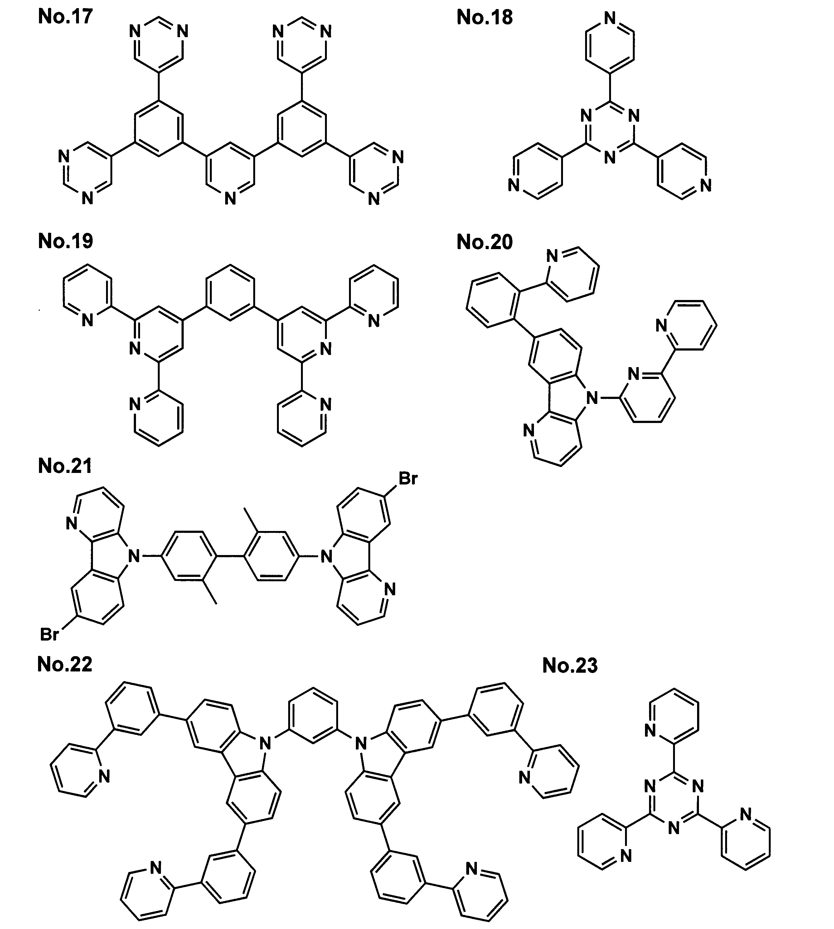
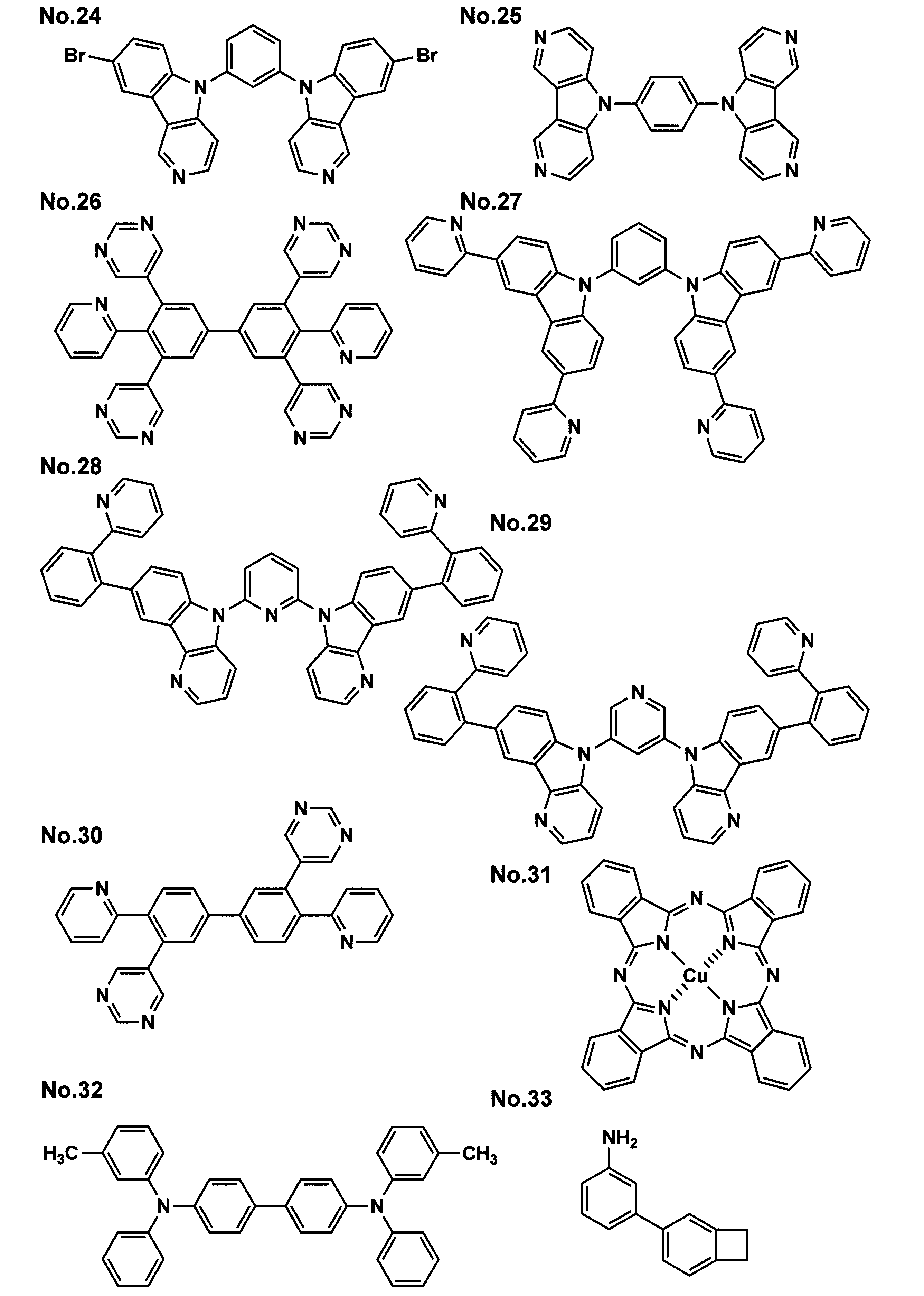


(1-2)窒素原子を有するポリマー
本発明においては、窒素原子を有する有機化合物として、ポリマーを用いることもできる。窒素原子を有するポリマーは、重量平均分子量が1000~1000000の範囲内であることが好ましい。


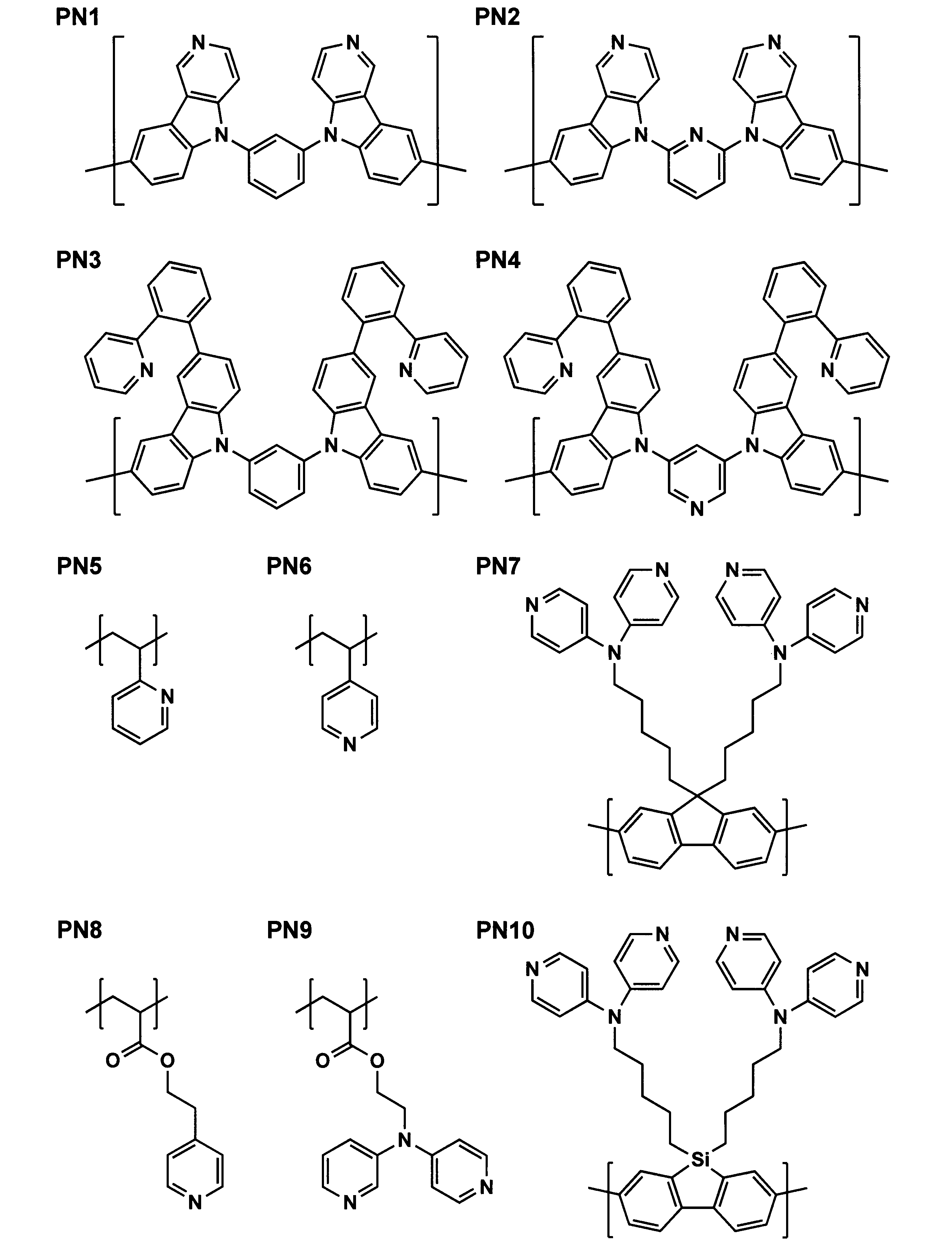


本発明に係る硫黄原子を有する有機化合物は、分子内に、スルフィド結合、ジスルフィド結合、メルカプト基、スルホン基、チオカルボニル結合等を有している。これらの中でも、スルフィド結合又はメルカプト基を有していることが好ましい。





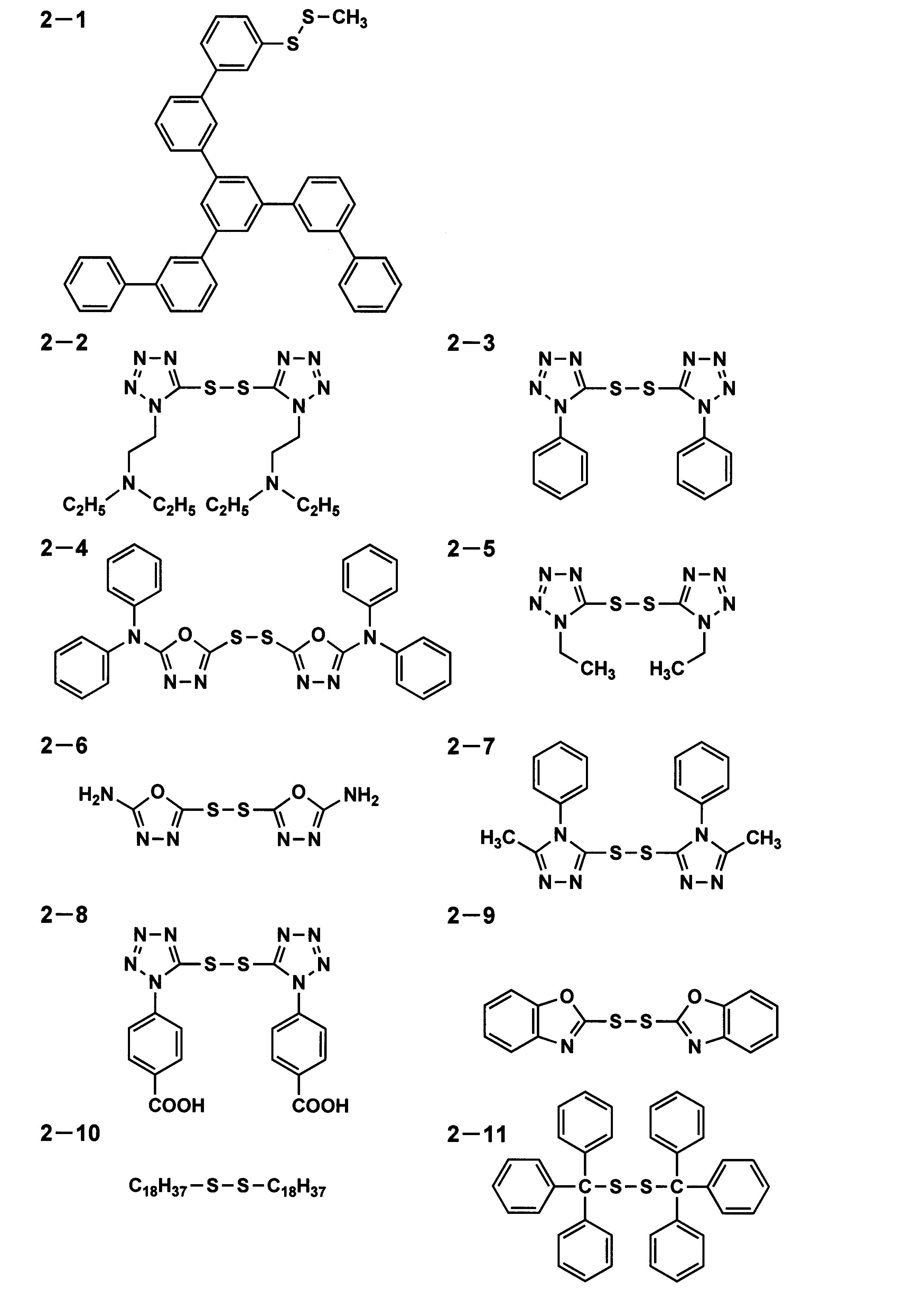


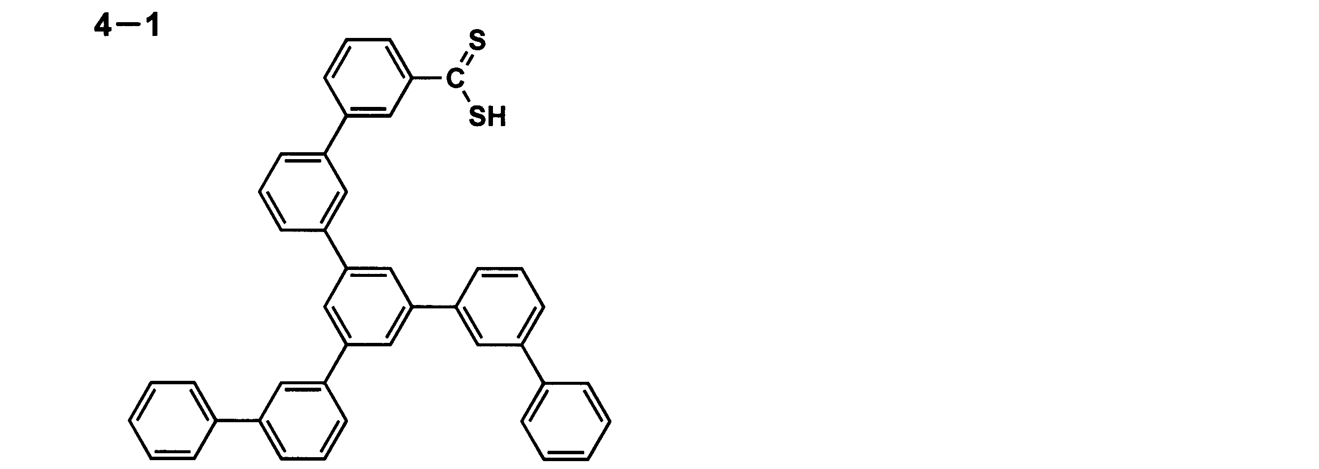
本発明においては、硫黄原子を有する有機化合物として、ポリマーを用いることもできる。
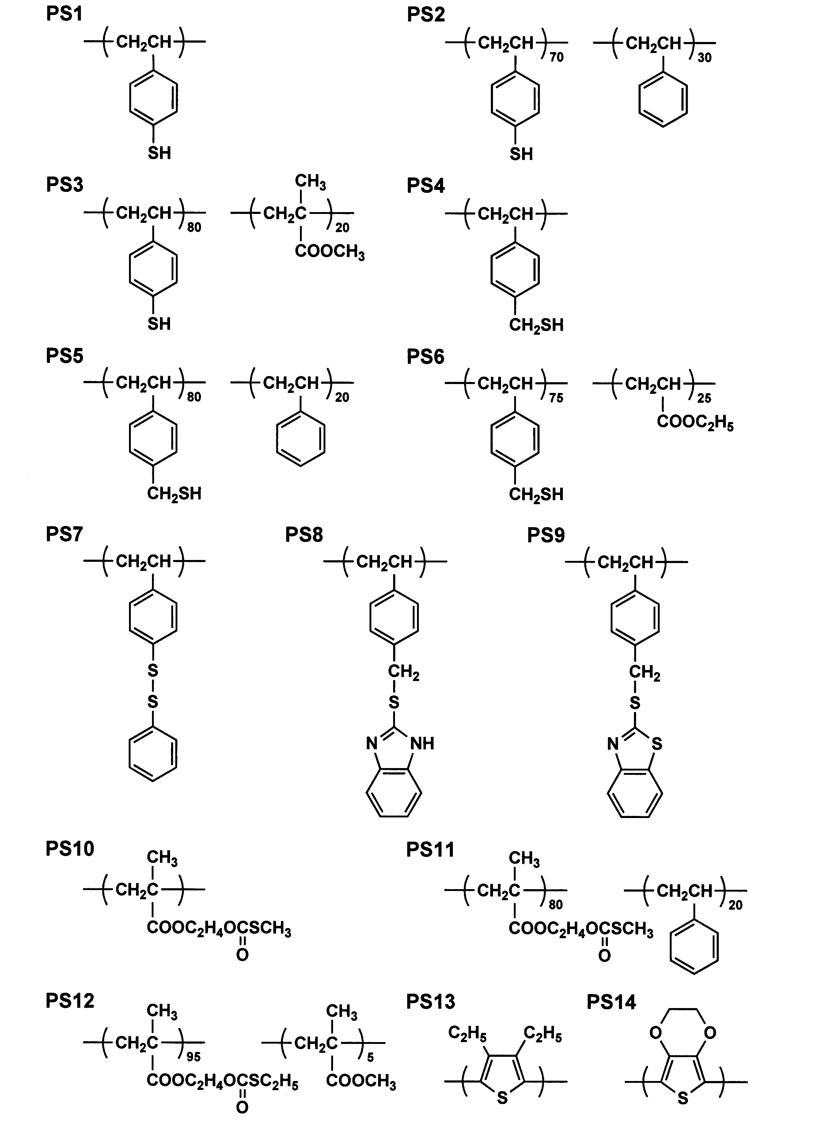
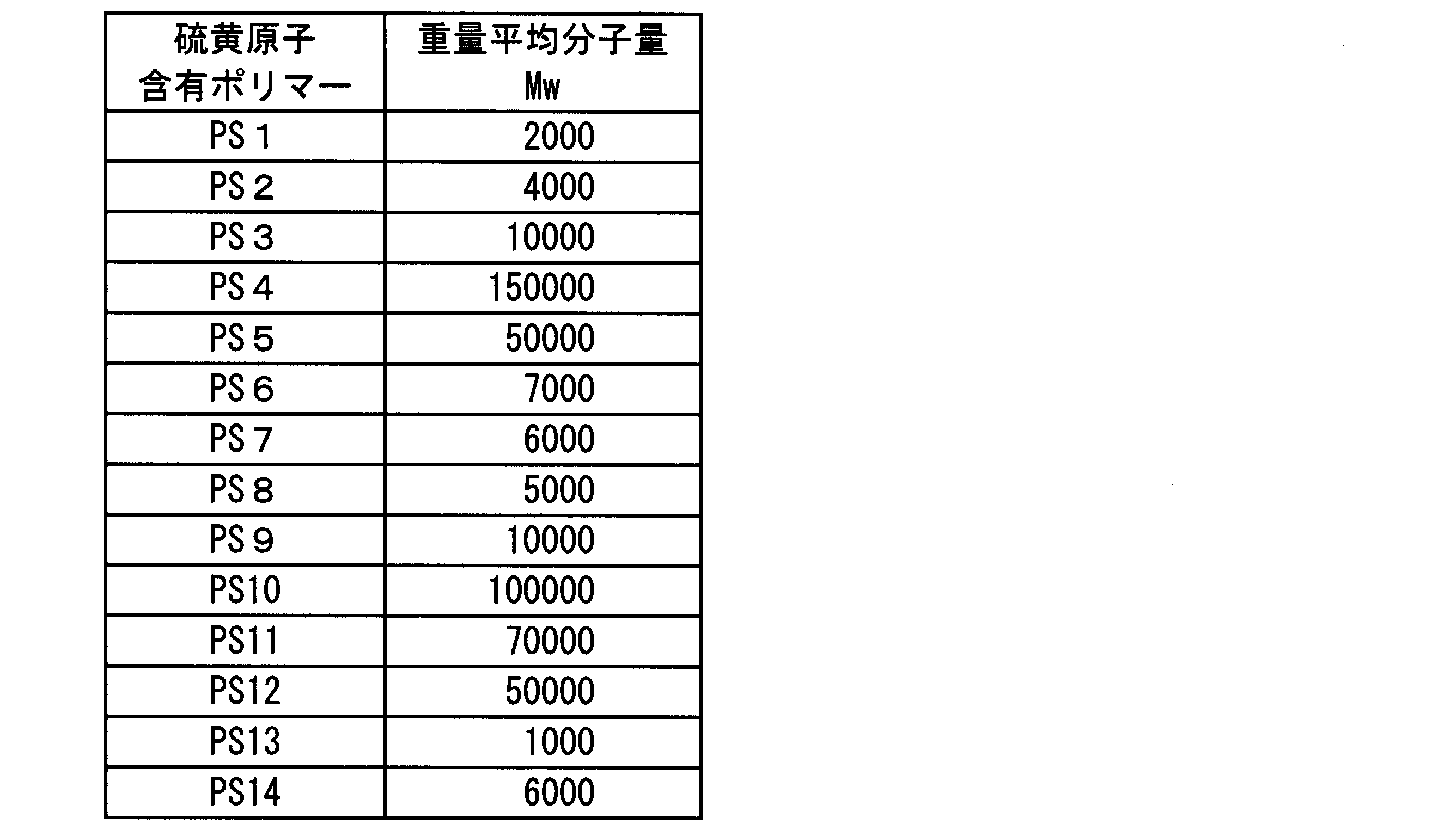
(測定条件)
装置:東ソー高速GPC装置 HLC-8220GPC
カラム:TOSOH TSKgel Super HM-M
検出器:RI及び/又はUV
溶出液流速:0.6ml/分
温度:30℃
試料濃度:0.1質量%
試料量:100μl
検量線:標準ポリスチレンにて作製(標準ポリスチレンSTK standard ポリスチレン(東ソー(株)製)Mw=500~1000000までの13サンプルを用いて検量線(校正曲線ともいう。)を作成し、測定対象物の重量平均分子量の算出に使用した。ここで、サンプルに用いたポリスチレンの重量平均分子量は、ほぼ等間隔に設定した。)
(2)電極層
電極層101bは、好ましくは銀又は銀を主成分とした合金を用いて構成された層であって、下地層101a上に成膜された層であることが好ましい。
以上のような構成の第一透明電極101は、例えば、窒素原子及び硫黄原子から選択される少なくとも1種の原子を有する有機化合物を用いて構成された下地層101a上に、銀又は銀を主成分とする合金からなる電極層101bを設けた構成である。これにより、下地層101aの上部に電極層101bを成膜する際には、電極層101bを構成する銀原子が下地層101aを構成する窒素原子又は硫黄原子を含んだ化合物と相互作用し、銀原子の下地層101a表面においての拡散距離が減少し、銀の凝集が抑えられる。
(1)発光層
有機発光層103には少なくとも発光層103cが含まれる。
ここで、本発明においてホスト化合物とは、発光層に含有される化合物の内でその層中での質量比が20%以上であり、かつ室温(25℃)においてリン光発光のリン光量子収率が、0.1未満の化合物と定義される。好ましくはリン光量子収率が0.01未満である。また、発光層に含有される化合物の中で、その層中での質量比が20%以上であることが好ましい。
本発明に用いられる発光ドーパントについて説明する。
本発明に用いられるリン光ドーパントは、励起三重項からの発光が観測される化合物であり、具体的には、室温(25℃)にてリン光発光する化合物であり、リン光量子収率が、25℃において0.01以上の化合物であると定義されるが、好ましいリン光量子収率は0.1以上である。
蛍光性化合物としては、クマリン系色素、ピラン系色素、シアニン系色素、クロコニウム系色素、スクアリウム系色素、オキソベンツアントラセン系色素、フルオレセイン系色素、ローダミン系色素、ピリリウム系色素、ペリレン系色素、スチルベン系色素、ポリチオフェン系色素、又は希土類錯体系蛍光体等が挙げられる。
注入層とは、駆動電圧低下や発光輝度向上のために電極と発光層103cの間に設けられる層のことで、「有機EL素子とその工業化最前線(1998年11月30日エヌ・ティー・エス社発行)」の第2編第2章「電極材料」(123~166頁)に詳細に記載されており、正孔注入層103aと電子注入層103eとがある。
正孔輸送層103bは、正孔を輸送する機能を有する正孔輸送材料からなり、広い意味で正孔注入層103a、電子阻止層も正孔輸送層103bに含まれる。正孔輸送層103bは単層又は複数層設けることができる。
電子輸送層103dは、電子を輸送する機能を有する材料からなり、広い意味で電子注入層103e、正孔阻止層(図示略)も電子輸送層103dに含まれる。電子輸送層103dは単層構造又は複数層の積層構造として設けることができる。
阻止層は、有機発光層103として、上記各機能層の他に、更に設けられていてもよい。例えば、特開平11-204258号公報、同11-204359号公報、及び「有機EL素子とその工業化最前線(1998年11月30日エヌ・ティー・エス社発行)」の237頁等に記載されている正孔阻止(ホールブロック)層がある。
正孔を輸送しつつ電子を阻止することで電子と正孔の再結合確率を向上させることができる。また、正孔輸送層103bの構成を必要に応じて電子阻止層として用いることができる。本発明に用いられる正孔阻止層の層厚としては、好ましくは3~100nmの範囲であり、さらに好ましくは5~30nmの範囲である。
第二透明電極102は、有機発光層103に電子を供給するカソードとして機能する電極膜であり、金属、合金、有機又は無機の導電性化合物、及びこれらの混合物が用いられる。
取り出し電極は、第一透明電極101及び第二透明電極102と外部電源とを電気的に接続するものであって、その材料としては特に限定されるものではなく公知の素材を好適に使用できるが、例えば、3層構造からなるMAM電極(Mo/Al・Nd合金/Mo)等の金属膜を用いることができる。
補助電極は、第一透明電極101及び第二透明電極102の抵抗を下げる目的で設けるものであって、第一透明電極101の電極層101b及び第二透明電極102の電極層に接して設けられる。補助電極を形成する材料は、金、白金、銀、銅、アルミニウム等の抵抗が低い金属が好ましい。これらの金属は光透過性が低いため、光取り出し面からの発光光hの取り出しの影響のない範囲でパターン形成される。
本発明に係る透明機能層の少なくとも1層として、前記第二透明電極102と前記透明封止基材105の間には、有機又は無機の化合物を含有する電極保護層104を形成することが、当該第二透明電極の表面を平滑にし、かつ機械的な保護を十分にするため、好ましい。また、透明封止基材をラミネートする際に、固体封止されるために接着強度が高い。
本発明に係る透明封止基材105は、可撓性を有し、かつ前記透明基板110と同一の材料群から選択される材料によって構成され、その機能としては、有機EL素子100をラミネート封止するものであり、図示例のように、例えば接着剤を含有する接着層(不図示)によって、電極保護層104側及び透明基板110側に固定されるものである。このような透明封止基材105は、有機EL素子100における第一透明電極101及び第二透明電極102の端子部分を露出させ、少なくとも有機発光層103を完全に覆う状態で設けられる。
本発明に用いられる樹脂基材は、透明であって、かつ可撓性樹脂基材である。本発明で好ましく用いられる樹脂基材は、有機EL素子に必要な耐湿性/耐気体透過性等のガスバリアー性能を有することが好ましい。
ガスバリアー層は、透明基板110と同一のガスバリアー層を設けることが、屈折率を制御する観点から好ましく、樹脂基板上に、少なくとも1層の無機前駆体化合物を含有する塗布液が塗布され、次いで真空紫外線照射によって改質処理を施したガスバリアー層であることが好ましい。中でもポリシラザンを含有する塗布液を塗布し、真空紫外線照射によって酸化ケイ素に改質処理した層であることが好ましい。
透明封止基材105によるラミネート封止する方法は、特に限定されるものではないが、例えば上記有機EL素子100を酸素及び水分濃度が一定の環境下(例えば、酸素濃度10ppm以下、水分濃度10ppm以下のグローブボックス内等)に置き、減圧下(1×10⁻³MPa以下)で吸引しながら加重をかけてプレスして、透明封止基材105に形成した接着層によって当該有機EL素子100をラミネート封止し、その後、熱風循環式オーブン、赤外線ヒーター、ヒートガン、高周波誘導加熱装置、ヒートツールの圧着による加熱等によって、当該接着層を熱硬化することによって行われる。
本発明の有機EL素子は、面発光体であり、両面発光型であるため各種の発光光源として用いることができる。例えば、家庭用照明や車内照明等の照明装置、時計や液晶用のバックライト、看板広告用照明、信号機の光源、光記憶媒体の光源、電子写真複写機の光源、光通信処理機の光源、光センサーの光源等で、両面発光型である特徴を活かした使用方法が挙げられる。
〔有機EL素子101の作製〕
(ガラス基板の洗浄)
ガラス基板の洗浄は、それぞれクラス10000のクリーンルーム内と、クラス100のクリーンブース内にて行った。洗浄溶媒は半導体洗浄用洗剤及び超純水(18MΩ以上、全有機炭素(TOC):10ppb未満)を用い、超音波洗浄機とUV洗浄機を用いた。
可撓性を有する厚さ70μmの薄膜ガラス基板上に、厚さ150nmのITO(酸化インジウム・スズ(Indiumu Tin Oxide:ITO))をスパッタ法により成膜し、フォトリソグラフィー法によりパターニングを行い、第一透明電極を形成した。なお、パターンは発光面積が50mm平方になるようなパターンとした。
(正孔輸送層の形成)
正孔輸送層形成用塗布液を塗布する前に、第一透明電極が形成されたガラス基板の洗浄表面改質処理を、光波長184.9nmの低圧水銀ランプを使用し、照射強度15mW/cm2、距離10mmで実施した。帯電除去処理は、微弱X線による除電器を使用し行った。
ポリエチレンジオキシチオフェン・ポリスチレンスルホネート(PEDOT/PSS、Bayer社製 Bytron P AI 4083)を純水で65%、メタノール5%で希釈した溶液を正孔輸送層形成用塗布液として準備した。
正孔輸送層形成用塗布液を塗布した後、成膜面に向け高さ100mm、吐出風速1m/s、幅手の風速分布5%、温度100℃で溶媒を除去した後、引き続き、加熱処理装置を用い温度150℃で裏面伝熱方式の熱処理を行い、正孔輸送層を形成した。
上記で形成した正孔輸送層上に、以下に示す白色発光層形成用塗布液を、下記の条件によりスピンコーターで塗布した後、下記の条件で乾燥及び加熱処理を行い、発光層を形成した。白色発光層形成用塗布液は乾燥後の厚さが40nmになるように塗布した。
ホスト材として下記化学構造式H-Aで表される化合物1.0gと、ドーパント材として下記化学構造式D-Aで表される化合物を100mg、ドーパント材として下記化構造学式D-Bで表される化合物を0.2mg、ドーパント材として下記化学構造式D-Cで表される化合物を0.2mg、100gのトルエンに溶解し白色発光層形成用塗布液として準備した。
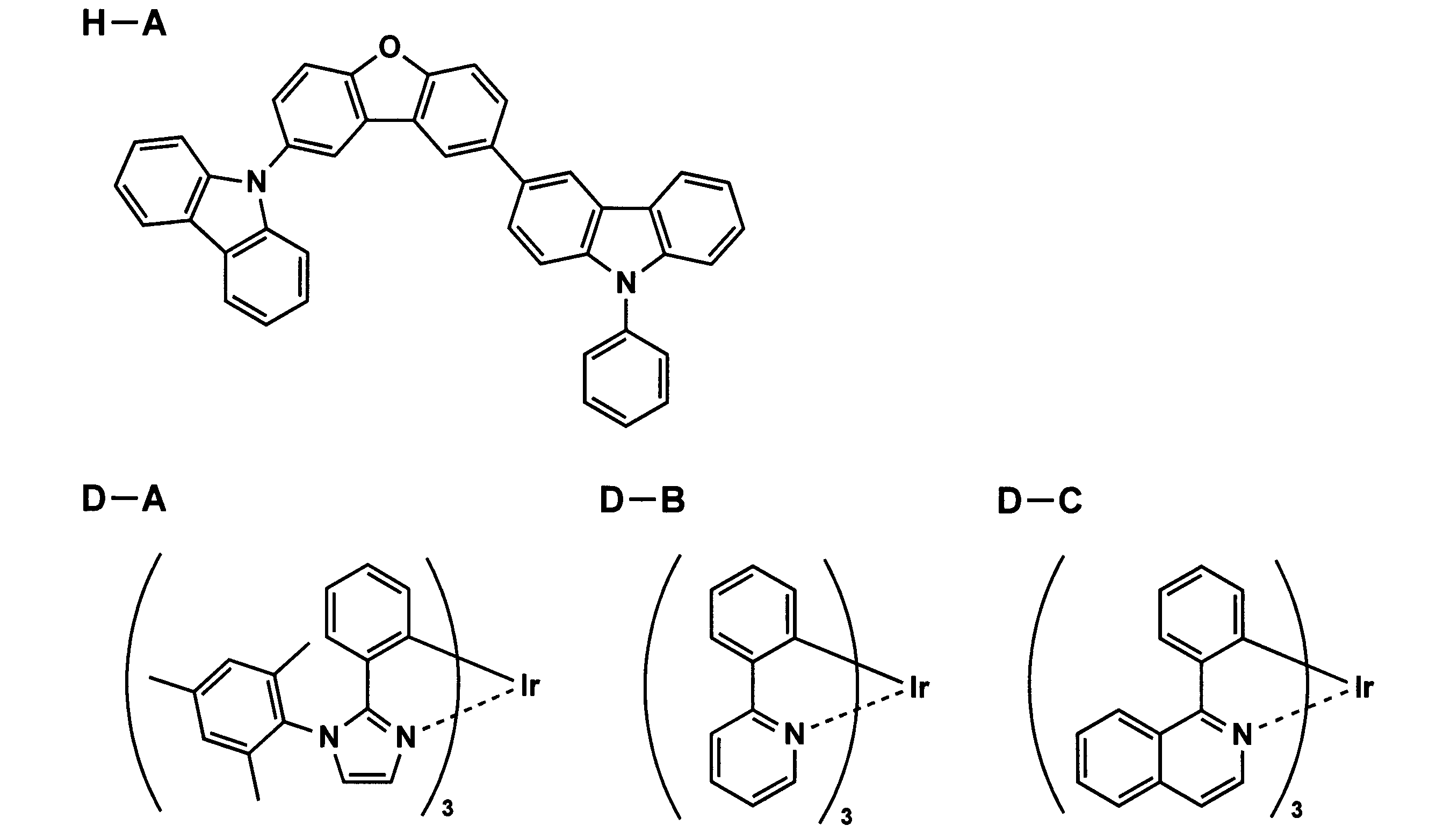
塗布工程を窒素ガス濃度99%以上の雰囲気で、塗布温度を25℃とした。
白色発光層形成用塗布液を塗布した後、成膜面に向け高さ100mm、吐出風速1m/s、幅手の風速分布5%、温度60℃で溶媒を除去した後、引き続き、温度130℃で加熱処理を行い、発光層を形成した。
上記で形成した発光層の上に、以下に示す電子輸送層形成用塗布液を下記の条件によりスピンコーターで塗布した後、下記の条件で乾燥及び加熱処理し、電子輸送層を形成した。電子輸送層形成用塗布液は、乾燥後の厚さが30nmになるように塗布した。
塗布工程は窒素ガス濃度99%以上の雰囲気で、電子輸送層形成用塗布液の塗布温度を25℃とした。
電子輸送層は下記化学構造式E-Aで表される化合物を2,2,3,3-テトラフルオロ-1-プロパノール中に溶解し0.5質量%溶液とし電子輸送層形成用塗布液とした。
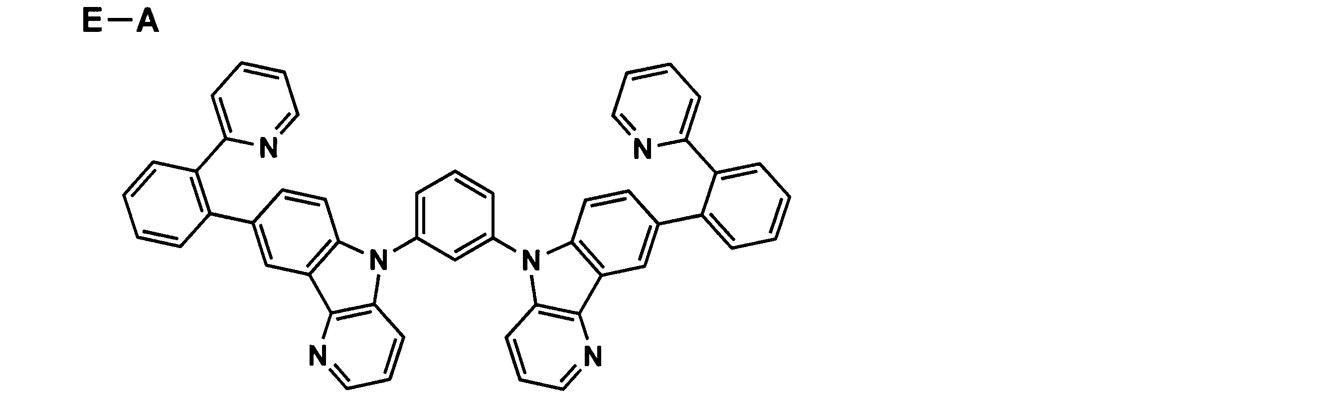
電子輸送層形成用塗布液を塗布した後、成膜面に向け高さ100mm、吐出風速1m/s、幅手の風速分布5%、温度60℃で溶媒を除去した後、引き続き、加熱処理部で、温度200℃で加熱処理を行い、電子輸送層を形成した。
上記で形成した電子輸送層上に、電子注入層を形成した。まず、基板を減圧チャンバー
に投入し、5×10⁻⁴Paまで減圧した。あらかじめ、真空チャンバー にタンタル製蒸着ボートに用意しておいたフッ化セシウムを加熱し、厚さ3nmの電子注入層を形成した。
上記で形成した電子注入層の上であって、第一透明電極の取り出し電極になる部分を除く部分に、5×10⁻⁴Paの真空下で、第二透明電極形成材料としてITOを使用し、取り出し電極を有するように蒸着法にて、発光面積が50mm平方になるようにマスクパターン成膜し、厚さ150nmの第二透明電極を積層した。
以上のように、第二透明電極までが形成された各積層体を、再び窒素雰囲気に移動し、規定の大きさに、紫外線レーザーを用いて裁断し、有機EL素子を作製した。
作製した有機EL素子に、ソニーケミカル&インフォメーションデバイス株式会社製の異方性導電フィルムDP3232S9を用いて、可撓性プリント基板(ベースフィルム:ポリイミド12.5μm、圧延銅箔18μm、カバーレイ:ポリイミド12.5μm、表面処理NiAuメッキ)を接続した。
上記作製した有機EL素子を、可撓性を有しない厚さ300μmの箱形の厚膜ガラス基板からなる透明封止基材で覆い、有機EL素子と封止材との間に中空部分を有する状態で、透明封止基材105の端部と透明基板110との間に接着剤(シール材)を充填した。接着剤としては、エポキシ系光硬化型接着剤(東亞合成社製ラックストラックLC0629B)を用いた。透明封止基材105と透明基板110との間に充填した接着剤に対して、厚膜ガラス基板(封止材)側からUV光を照射し、接着剤を硬化させて有機EL素子を封止して、有機EL素子101を作製した。
(透明基板の作製)
両面に易接着加工された幅500mm、厚さ125μmのポリエステルフィルム(帝人デュポンフィルム株式会社製、極低熱収PET)上に、ポリシラザン含有塗布液を塗布し、次いで真空紫外線を照射して改質処理を行い、ガスバリアー層を設けて、可撓性透明基板を作製した。表中、PHPSバリアと記載する。
無触媒のパーヒドロポリシラザンを20質量%含むジブチルエーテル溶液(AZエレクトロニックマテリアルズ株式会社製、アクアミカ(登録商標)NN120-20)と、アミン触媒(N,N,N′,N′-テトラメチル-1,6-ジアミノヘキサン(TMDAH))5質量%を含むパーヒドロポリシラザン20質量%のジブチルエーテル溶液(AZエレクトロニックマテリアルズ株式会社製、アクアミカ(登録商標)NAX120-20)とを、4:1の割合で混合し、さらにジブチルエーテルと2,2,4-トリメチルペンタンとの質量比が65:35となるように混合した溶媒で、塗布液の固形分が5質量%になるように、塗布液を希釈調製した。
真空紫外線照射は、図2に模式図で示した装置を用いて行った。
有機EL素子102の作製において、透明基板として前記厚さ70μmの薄膜ガラスを用い、透明封止基材として前記ガスバリアー層付きPET基材を用いた以外は同様にして、有機EL素子103を作製した。
有機EL素子103の作製において、透明基板及び透明封止基材として、ともに前記ガスバリアー層付きPET基材を用いた以外は同様にして、有機EL素子104を作製した。
有機EL素子104の作製において用いた前記ガスバリアー層付きPET基材を、透明基板として用いて、当該ガスバリアー層上に単層構造の第一透明電極を以下のように作製した。
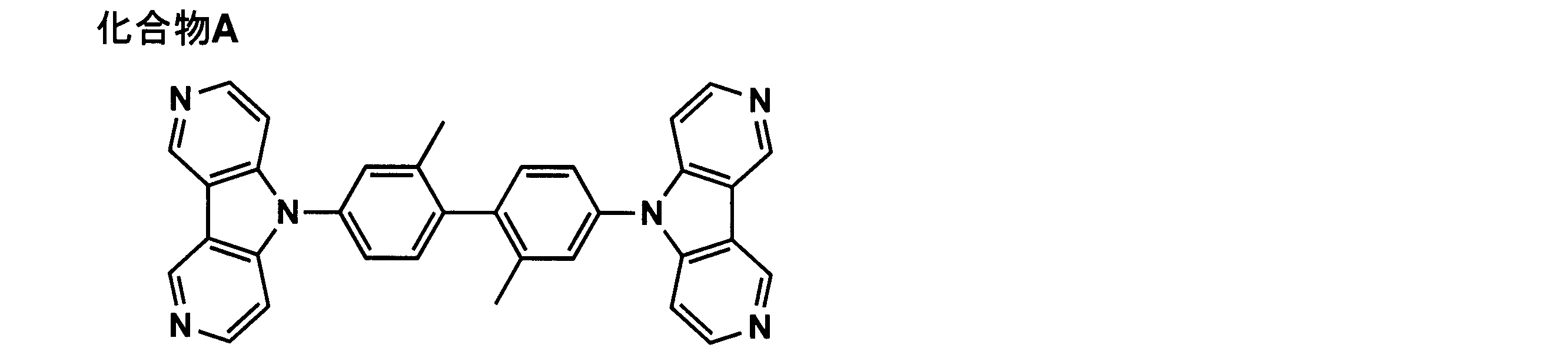
有機EL素子105の作製において用いた前記ガスバリアー層付きPET基材を、透明基板として用いて、当該ガスバリアー層上に単層構造の第一透明電極を以下のように作製した。
有機EL素子105の作製と同様にして前記化合物Aを含有する下地層を形成し、次いで、有機EL素子106と同様にして、タングステン製の抵抗加熱ボートに銀(Ag)を入れ、真空槽を4×10⁻⁴Paまで減圧した後、抵抗加熱ボートを通電して加熱し、銀からなる単層構造の第一透明電極を抵抗加熱蒸着にて形成した。形成された銀(Ag)からなる第一透明電極の層厚は10nmであった。
有機EL素子107の作製において、第一透明電極及び第二透明電極に用いる金属を銀(Ag)とアルミニウム(Al)が98:2の原子数比となるように共蒸着て形成した以外は、同様にして有機EL素子108を作製した。
〔電力効率の測定〕
分光放射輝度計CS-1000(コニカミノルタ社製)を用いて、各有機EL素子の正面輝度及び輝度角度依存性を5°毎に±80°の角度まで測定し、正面輝度換算1000cd/m2における電力効率を、第一透明電極側(基板側)、及び第二透明電極側(封止側)でそれぞれ求めた。
分光放射輝度計CS-1000(コニカミノルタ社製)を用いて、各有機EL素子の色度の角度依存性を、正面及び5°毎に±80°の角度まで測定し、その正面との色ずれΔEが最大となる時のΔEの値を下記式より、第一透明電極側(基板側)、及び第二透明電極側(封止側)でそれぞれ求めた。なお、下記式においてx、yは、CIE1931表色系における色度x、yである。
上記測定したΔExyについて有機EL素子104の第一透明電極側の測定値を100とする相対値で表し、値が小さいほど視野角の変化による色ずれが小さいことを表す。

実施例1で作製した有機EL素子104、105、106、及び107において、構成する有機発光層の各層の層厚を適宜変化させて、第一透明電極と前記有機発光層の発光中心との距離をa、第二透明電極と有機発光層の発光中心との距離をbとしたときの比a:bの値を下記表4に記載のように変化させて、それぞれ上記有機EL素子に対応する、有機EL素子204、205、206、及び207を作製した。

実施例1で作製した有機EL素子106、107、及び108において、構成する第一透明電極の金属層の層厚、及び第二透明電極の金属層の層厚を、下記表5のようにさせて、それぞれ上記有機EL素子に対応する、有機EL素子306、316、307、及び308を作製した。

101 第一透明電極
101a 下地層
101b 電極層
102 第二透明電極(対向電極)
103 有機発光層
103a 正孔注入層
103b 正孔輸送層
103c 発光層
103d 電子輸送層
103e 電子注入層
104 電極保護層
105 透明封止基材
110 透明基板
h 発光光
Claims (8)
- 少なくとも透明基板、第一透明電極、有機発光層、第二透明電極及び透明封止基材で構成される有機エレクトロルミネッセンス素子であって、当該透明基板と当該透明封止基材とがいずれも可撓性を有し、同一の材料群から選択される材料によって構成され、かつ、当該第一透明電極と当該第二透明電極とが同一の材料群から選択される材料によって構成されていることを特徴とする有機エレクトロルミネッセンス素子。
- 前記第一透明電極及び前記第二透明電極が、いずれも銀又は銀を主成分とする合金を含有することを特徴とする請求項1に記載の有機エレクトロルミネッセンス素子。
- 前記透明基板と前記第一透明電極の間、及び前記第二透明電極と前記透明封止基材との間に有機又は無機の化合物を含有する透明機能層を有することを特徴とする請求項1又は請求項2に記載の有機エレクトロルミネッセンス素子。
- 前記透明機能層の少なくとも1層が、窒素原子及び硫黄原子から選択される少なくとも1種の原子を有する有機化合物を含有する下地層であることを特徴とする請求項3に記載の有機エレクトロルミネッセンス素子。
- 前記透明機能層の少なくとも1層が、電極保護層であることを特徴とする請求項3に記載の有機エレクトロルミネッセンス素子。
- 前記第一透明電極及び前記第二透明電極の層厚が、それぞれ5~30nmの範囲内であることを特徴とする請求項1から請求項5までのいずれか一項に記載の有機エレクトロルミネッセンス素子。
- 前記透明基板上に配置される、前記第一透明電極、前記有機発光層、及び前記第二透明電極の全体が、前記透明封止基材によってラミネート封止されていることを特徴とする請求項1から請求項6までのいずれか一項に記載の有機エレクトロルミネッセンス素子。
- 前記第一透明電極と前記有機発光層の発光中心との距離をaとし、前記第二透明電極と前記有機発光層の発光中心との距離をbとしたとき、比a:bが3:5~5:3の範囲内であることを特徴とする請求項1から請求項7までのいずれか一項に記載の有機エレクトロルミネッセンス素子。
Priority Applications (2)
| Application Number | Priority Date | Filing Date | Title |
|---|---|---|---|
| US14/895,425 US10069099B2 (en) | 2013-06-06 | 2014-05-15 | Organic electroluminescence element |
| JP2015521364A JP6390613B2 (ja) | 2013-06-06 | 2014-05-15 | 有機エレクトロルミネッセンス素子 |
Applications Claiming Priority (2)
| Application Number | Priority Date | Filing Date | Title |
|---|---|---|---|
| JP2013119615 | 2013-06-06 | ||
| JP2013-119615 | 2013-06-06 |
Publications (1)
| Publication Number | Publication Date |
|---|---|
| WO2014196330A1 true WO2014196330A1 (ja) | 2014-12-11 |
Family
ID=52007983
Family Applications (1)
| Application Number | Title | Priority Date | Filing Date |
|---|---|---|---|
| PCT/JP2014/062916 Ceased WO2014196330A1 (ja) | 2013-06-06 | 2014-05-15 | 有機エレクトロルミネッセンス素子 |
Country Status (3)
| Country | Link |
|---|---|
| US (1) | US10069099B2 (ja) |
| JP (1) | JP6390613B2 (ja) |
| WO (1) | WO2014196330A1 (ja) |
Cited By (2)
| Publication number | Priority date | Publication date | Assignee | Title |
|---|---|---|---|---|
| KR20160103596A (ko) * | 2015-02-24 | 2016-09-02 | 삼성디스플레이 주식회사 | 유기 발광 소자 |
| WO2017056635A1 (ja) * | 2015-09-30 | 2017-04-06 | コニカミノルタ株式会社 | 有機エレクトロルミネッセンス素子 |
Families Citing this family (3)
| Publication number | Priority date | Publication date | Assignee | Title |
|---|---|---|---|---|
| WO2019147640A1 (en) * | 2018-01-25 | 2019-08-01 | Kulicke And Soffa Industries, Inc. | Bonding tools for bonding machines, bonding machines for bonding semiconductor elements, and related methods |
| CN109148728B (zh) * | 2018-08-31 | 2019-10-29 | 昆山国显光电有限公司 | 一种显示面板及显示装置 |
| TWI694748B (zh) * | 2019-08-28 | 2020-05-21 | 明志科技大學 | 用以產生大面積電漿之電極元件 |
Citations (5)
| Publication number | Priority date | Publication date | Assignee | Title |
|---|---|---|---|---|
| JP2003077680A (ja) * | 2001-09-06 | 2003-03-14 | Konica Corp | 有機エレクトロルミネッセンス素子及び表示装置 |
| JP2004146379A (ja) * | 2002-10-22 | 2004-05-20 | Osram Opto Semiconductors Gmbh | 実質的に透明でありかつ導電性を有する電極および該電極の作製方法ならびに該電極を含む有機電子デバイス |
| JP2011077028A (ja) * | 2009-09-04 | 2011-04-14 | Hitachi Displays Ltd | 有機el表示装置 |
| WO2013073356A1 (ja) * | 2011-11-17 | 2013-05-23 | コニカミノルタ株式会社 | 透明電極、および電子デバイス |
| JP2013242988A (ja) * | 2012-05-18 | 2013-12-05 | Konica Minolta Inc | 有機エレクトロルミネッセンス発光体 |
Family Cites Families (8)
| Publication number | Priority date | Publication date | Assignee | Title |
|---|---|---|---|---|
| GB2421117B (en) * | 2002-09-17 | 2006-09-27 | Dainippon Printing Co Ltd | Method of manufacturing a light emitting display panel and a light emitting diplay panel |
| JP4531341B2 (ja) | 2003-02-28 | 2010-08-25 | 株式会社半導体エネルギー研究所 | 発光装置および電子機器 |
| DE102006046196A1 (de) | 2006-09-29 | 2008-04-03 | Osram Opto Semiconductors Gmbh | Leuchtmittel |
| US20080138538A1 (en) * | 2006-12-06 | 2008-06-12 | General Electric Company | Barrier layer, composite article comprising the same, electroactive device, and method |
| JP4798671B2 (ja) | 2009-03-27 | 2011-10-19 | 有限会社 Q−Lights | 両面発光有機エレクトロルミネッセンス照明装置 |
| JP5640365B2 (ja) * | 2009-12-07 | 2014-12-17 | ソニー株式会社 | 表示装置及び表示装置の制御方法 |
| US8664518B2 (en) * | 2009-12-11 | 2014-03-04 | Konica Minolta Holdngs, Inc. | Organic photoelectric conversion element and producing method of the same |
| JP2012227122A (ja) * | 2011-04-04 | 2012-11-15 | Rohm Co Ltd | 有機el装置 |
-
2014
- 2014-05-15 WO PCT/JP2014/062916 patent/WO2014196330A1/ja not_active Ceased
- 2014-05-15 JP JP2015521364A patent/JP6390613B2/ja not_active Expired - Fee Related
- 2014-05-15 US US14/895,425 patent/US10069099B2/en not_active Expired - Fee Related
Patent Citations (5)
| Publication number | Priority date | Publication date | Assignee | Title |
|---|---|---|---|---|
| JP2003077680A (ja) * | 2001-09-06 | 2003-03-14 | Konica Corp | 有機エレクトロルミネッセンス素子及び表示装置 |
| JP2004146379A (ja) * | 2002-10-22 | 2004-05-20 | Osram Opto Semiconductors Gmbh | 実質的に透明でありかつ導電性を有する電極および該電極の作製方法ならびに該電極を含む有機電子デバイス |
| JP2011077028A (ja) * | 2009-09-04 | 2011-04-14 | Hitachi Displays Ltd | 有機el表示装置 |
| WO2013073356A1 (ja) * | 2011-11-17 | 2013-05-23 | コニカミノルタ株式会社 | 透明電極、および電子デバイス |
| JP2013242988A (ja) * | 2012-05-18 | 2013-12-05 | Konica Minolta Inc | 有機エレクトロルミネッセンス発光体 |
Cited By (4)
| Publication number | Priority date | Publication date | Assignee | Title |
|---|---|---|---|---|
| KR20160103596A (ko) * | 2015-02-24 | 2016-09-02 | 삼성디스플레이 주식회사 | 유기 발광 소자 |
| CN113241413A (zh) * | 2015-02-24 | 2021-08-10 | 三星显示有限公司 | 有机发光装置 |
| KR102318419B1 (ko) * | 2015-02-24 | 2021-10-28 | 삼성디스플레이 주식회사 | 유기 발광 소자 |
| WO2017056635A1 (ja) * | 2015-09-30 | 2017-04-06 | コニカミノルタ株式会社 | 有機エレクトロルミネッセンス素子 |
Also Published As
| Publication number | Publication date |
|---|---|
| US20160111676A1 (en) | 2016-04-21 |
| US10069099B2 (en) | 2018-09-04 |
| JPWO2014196330A1 (ja) | 2017-02-23 |
| JP6390613B2 (ja) | 2018-09-19 |
Similar Documents
| Publication | Publication Date | Title |
|---|---|---|
| JP2013110262A (ja) | 有機el素子ならびに有機elモジュールおよびその製造方法 | |
| WO2012121101A1 (ja) | 有機エレクトロルミネッセンス素子 | |
| WO2013141097A1 (ja) | 透明電極、電子デバイス及び有機エレクトロルミネッセンス素子 | |
| WO2014069256A1 (ja) | 有機エレクトロルミネッセンス素子 | |
| JP6390613B2 (ja) | 有機エレクトロルミネッセンス素子 | |
| JP2008293680A (ja) | 有機エレクトロルミネッセンス素子及びその製造方法 | |
| JP2008282610A (ja) | 有機エレクトロルミネッセンス素子の製造方法 | |
| WO2018037880A1 (ja) | 透明電極及び電子デバイス | |
| JP6485350B2 (ja) | 有機エレクトロルミネッセンス素子の製造方法 | |
| WO2017056553A1 (ja) | 有機エレクトロルミネッセンス素子及びこれを備えた照明装置 | |
| JP2009076241A (ja) | 有機エレクトロルミネッセンス素子の製造方法 | |
| WO2013161750A1 (ja) | 透明電極、電子デバイス及び有機エレクトロルミネッセンス素子 | |
| WO2012077431A1 (ja) | 有機エレクトロルミネッセンス素子の製造方法 | |
| JP5939249B2 (ja) | 有機エレクトロルミネッセンス素子の製造方法 | |
| WO2013141190A1 (ja) | 有機エレクトロルミネッセンス素子用封止要素、有機エレクトロルミネッセンス素子の製造方法 | |
| JPWO2015068779A1 (ja) | 有機エレクトロルミネッセンス素子、有機エレクトロルミネッセンス素子の製造方法、及び有機エレクトロルミネッセンスモジュール | |
| WO2014192902A1 (ja) | 透明電極、電子デバイス及び有機エレクトロルミネッセンス素子 | |
| WO2014192589A1 (ja) | 有機エレクトロルミネッセンス素子、有機エレクトロルミネッセンス素子の製造方法、及び有機エレクトロルミネッセンスモジュール | |
| WO2014065226A1 (ja) | 透明電極、電子デバイス及び有機エレクトロルミネッセンス素子 | |
| JP2013074085A (ja) | 有機エレクトロルミネッセンス素子 | |
| JPWO2015115175A1 (ja) | 有機エレクトロルミネッセンス素子及びその製造方法 | |
| JP2013089608A (ja) | 有機el素子 | |
| WO2016136397A1 (ja) | 透明電極及び電子デバイス | |
| WO2014057796A1 (ja) | 透明電極、電子デバイス及び有機エレクトロルミネッセンス素子 | |
| JPWO2012002245A1 (ja) | 有機エレクトロルミネッセンス素子 |
Legal Events
| Date | Code | Title | Description |
|---|---|---|---|
| 121 | Ep: the epo has been informed by wipo that ep was designated in this application |
Ref document number: 14808164 Country of ref document: EP Kind code of ref document: A1 |
|
| ENP | Entry into the national phase |
Ref document number: 2015521364 Country of ref document: JP Kind code of ref document: A |
|
| WWE | Wipo information: entry into national phase |
Ref document number: 14895425 Country of ref document: US |
|
| NENP | Non-entry into the national phase |
Ref country code: DE |
|
| 122 | Ep: pct application non-entry in european phase |
Ref document number: 14808164 Country of ref document: EP Kind code of ref document: A1 |