WO2014196137A1 - 素子構造体及びその製造方法 - Google Patents
素子構造体及びその製造方法 Download PDFInfo
- Publication number
- WO2014196137A1 WO2014196137A1 PCT/JP2014/002661 JP2014002661W WO2014196137A1 WO 2014196137 A1 WO2014196137 A1 WO 2014196137A1 JP 2014002661 W JP2014002661 W JP 2014002661W WO 2014196137 A1 WO2014196137 A1 WO 2014196137A1
- Authority
- WO
- WIPO (PCT)
- Prior art keywords
- inorganic material
- element structure
- layer
- material layer
- resin material
- Prior art date
- Legal status (The legal status is an assumption and is not a legal conclusion. Google has not performed a legal analysis and makes no representation as to the accuracy of the status listed.)
- Ceased
Links
Images



Classifications
-
- H—ELECTRICITY
- H10—SEMICONDUCTOR DEVICES; ELECTRIC SOLID-STATE DEVICES NOT OTHERWISE PROVIDED FOR
- H10K—ORGANIC ELECTRIC SOLID-STATE DEVICES
- H10K50/00—Organic light-emitting devices
- H10K50/80—Constructional details
- H10K50/84—Passivation; Containers; Encapsulations
- H10K50/842—Containers
- H10K50/8426—Peripheral sealing arrangements, e.g. adhesives, sealants
-
- H—ELECTRICITY
- H10—SEMICONDUCTOR DEVICES; ELECTRIC SOLID-STATE DEVICES NOT OTHERWISE PROVIDED FOR
- H10K—ORGANIC ELECTRIC SOLID-STATE DEVICES
- H10K50/00—Organic light-emitting devices
- H10K50/80—Constructional details
- H10K50/84—Passivation; Containers; Encapsulations
- H10K50/844—Encapsulations
-
- H—ELECTRICITY
- H10—SEMICONDUCTOR DEVICES; ELECTRIC SOLID-STATE DEVICES NOT OTHERWISE PROVIDED FOR
- H10K—ORGANIC ELECTRIC SOLID-STATE DEVICES
- H10K71/00—Manufacture or treatment specially adapted for the organic devices covered by this subclass
-
- H—ELECTRICITY
- H10—SEMICONDUCTOR DEVICES; ELECTRIC SOLID-STATE DEVICES NOT OTHERWISE PROVIDED FOR
- H10K—ORGANIC ELECTRIC SOLID-STATE DEVICES
- H10K85/00—Organic materials used in the body or electrodes of devices covered by this subclass
- H10K85/10—Organic polymers or oligomers
- H10K85/141—Organic polymers or oligomers comprising aliphatic or olefinic chains, e.g. poly N-vinylcarbazol, PVC or PTFE
-
- H—ELECTRICITY
- H10—SEMICONDUCTOR DEVICES; ELECTRIC SOLID-STATE DEVICES NOT OTHERWISE PROVIDED FOR
- H10K—ORGANIC ELECTRIC SOLID-STATE DEVICES
- H10K2102/00—Constructional details relating to the organic devices covered by this subclass
Definitions
- the present invention relates to an element structure having a laminated structure that protects a device and the like from oxygen, moisture, and the like, and a method for manufacturing the element structure.
- an organic EL (Electro Luminescence) element or the like is known as an element containing a compound having a property that easily deteriorates due to moisture or oxygen.
- an attempt is made to suppress intrusion of moisture or the like into the element by forming a laminated structure with a protective layer covering the layer containing the compound.
- Patent Document 1 described below describes a light-emitting element having a protective film formed of a laminated film of an inorganic film and an organic film on an upper electrode layer.
- the coverage of an inorganic film having a barrier property such as water vapor is relatively low, and if the substrate surface having the device layer has irregularities, the irregularities cannot be sufficiently covered. There is a risk of failure. When the coating failure of the inorganic film occurs, it becomes impossible to prevent the intrusion of moisture from the inorganic film, so that it is difficult to ensure a sufficient barrier property.
- an object of the present invention is to provide an element structure that can improve barrier properties such as water vapor and a method for manufacturing the same.
- an element structure includes a base, a device layer, a convex portion, and a first resin material.
- the base has a first surface and a second surface opposite to the first surface.
- the device layer is disposed on at least the first surface of the first and second surfaces.
- the convex portion is formed on the first surface.
- the first resin material is unevenly distributed around the convex portion.
- the manufacturing method of the element structure which concerns on one form of this invention includes forming the convex part comprised by the 1st inorganic material layer which coat
- a liquid organic material is supplied to the surface of the substrate, and the organic material is aggregated at a boundary portion between the side surface of the convex portion and the surface of the substrate.
- a second inorganic material layer that covers the convex portion and the organic material is formed on the surface of the substrate.
- 1 is a schematic cross-sectional view showing an element structure according to a first embodiment of the present invention. It is a top view of the element structure. It is an expanded sectional view of the important section of the above-mentioned element structure. It is process drawing explaining the formation method of the 1st resin material in the said element structure. It is a schematic sectional drawing which shows the modification of a structure of the said element structure. It is a schematic sectional drawing which shows the element structure which concerns on the 2nd Embodiment of this invention. It is a schematic sectional drawing which shows the modification of a structure of the element structure which concerns on the said 1st Embodiment.
- An element structure includes a base, a device layer, a convex portion, and a first resin material.
- the base has a first surface and a second surface opposite to the first surface.
- the device layer is disposed on at least the first surface of the first and second surfaces.
- the convex portion is formed on the first surface.
- the first resin material is unevenly distributed around the convex portion.
- the first resin material is unevenly distributed around the convex portion formed on the substrate surface (first surface) on which the device layer is disposed, moisture from the convex portion, etc. Intrusion can be suppressed.
- the defective coating portion is covered with the first resin material even when the defective coating of the side surface of the device layer due to the convex portion occurs. Is possible.
- the material and form of the substrate are not particularly limited, and may be a substrate made of glass or semiconductor, or a film made of plastic or metal.
- the said convex part may contain a device layer and may be formed so that a device layer may be coat
- the configuration in which the convex portion includes the device layer includes a stacked body in which the convex portion includes the device layer, a structure in which a part of the device layer is exposed on the surface of the convex portion, and the like.
- the convex portion may be formed so as to cover the side surface of the device layer, or a plurality of convex portions may be formed on the upper surface of the device layer.
- the convex portion may be composed of a first inorganic material layer that covers the device layer.
- the element structure may further include a second inorganic material layer that covers the first resin material and the first inorganic material layer.
- the first inorganic material layer is provided on the surface (first surface) of the base so as to cover the surface and side surfaces of the device layer.
- the first inorganic material layer is typically composed of an inorganic material having a water vapor barrier property such as silicon nitride, silicon oxide, silicon oxynitride, aluminum oxide, or the like.
- the first inorganic material layer is typically formed by a sputtering method, an ALD method, a CVD method, or the like.
- the coverage is relatively low, for example, the boundary between the side surface of the device layer and the surface of the substrate The part may not be properly coated.
- the first resin material is unevenly distributed around the convex portion, that is, the boundary portion between the device layer side surface and the substrate surface, the boundary portion is appropriately covered with the first resin material. be able to.
- the second inorganic material layer is typically composed of an inorganic material having a water vapor barrier property such as silicon nitride, silicon oxide, silicon oxynitride, aluminum oxide or the like.
- the second inorganic material layer is typically formed by a sputtering method, an ALD method, a CVD method, or the like.
- the coverage of the first inorganic material layer with respect to the convex portion is improved. This makes it possible to configure an element structure that can suppress the intrusion of oxygen, moisture, and the like into the element.
- the method for forming the first resin material is not particularly limited.
- a liquid, gaseous or mist organic material is applied to the substrate surface by an appropriate coating method such as spraying, spin coating, or vapor deposition. Is done.
- the organic material immediately after application enters a minute gap due to a capillary phenomenon, or drops or aggregates due to its own surface tension, thereby being unevenly distributed at the boundary between the convex side surface and the substrate surface. Then, the said 1st resin material can be formed in the circumference
- the organic material constituting the first resin material is not particularly limited.
- the first resin material drops and aggregates on the substrate by its own surface tension, moves on the substrate, and is unevenly distributed around the convex portion.
- the resulting material is used.
- an acrylic resin, a polyurea resin, or the like is used as the organic material.
- the resin can be easily cured by using an organic material that is cured by irradiation with energy rays such as ultraviolet rays.
- the application condition of the organic material is not particularly limited, but it is preferable to limit the application amount so as not to prevent the organic material from being dropped or to prevent the organic material film from being formed.
- the substrate may be tilted or vibration may be applied to the substrate in order to promote the movement of the organic material around the convex portion.
- the element structure may further include a second resin material.
- the second resin material is interposed between the first inorganic material layer and the second inorganic material layer, and is unevenly distributed on the surface of the convex portion independently of the first resin material.
- the surface of the first inorganic material layer is not necessarily flat. For example, irregularities may be formed when particles or the like are mixed in the film during film formation. When particles are mixed in the first inorganic material layer, the coverage of the first inorganic material layer with respect to the device layer may be reduced, and the desired barrier characteristics may not be obtained. Therefore, the element structure has a structure in which the second resin material is filled in a poorly coated portion of the first inorganic material layer generated by mixing of particles or the like.
- the first resin material is unevenly distributed at the boundary between the surface of the first inorganic material layer and the peripheral surface of the particles. Thereby, the coverage of the device layer is enhanced, and the second inorganic material layer can be appropriately formed by the second resin material functioning as a base.
- the second resin material is formed by the same method as the first resin material.
- the second resin material may be made of the same organic material as the first resin material.
- the first resin material and the second resin material can be simultaneously formed in the same process.
- the organic material unevenly distributed at the boundary between the side surface of the convex portion and the surface of the base constitutes the first resin material
- the organic material unevenly distributed on the surface of the convex portion constitutes the second resin material.
- the manufacturing method of the element structure which concerns on one Embodiment of this invention includes forming the convex part comprised by the 1st inorganic material layer which coat
- a liquid organic material is supplied to the surface of the substrate, and the organic material is aggregated at a boundary portion between the side surface of the convex portion and the surface of the substrate.
- a second inorganic material layer that covers the convex portion and the organic material is formed on the surface of the substrate.
- the organic material applied to the substrate surface enters a fine gap due to a capillary phenomenon, and further drops or agglomerates by its own surface tension, so that the convex peripheral surface and the substrate surface It is unevenly distributed at the boundary. Thereafter, an organic material aggregate (resin material) can be formed at the boundary by curing the organic material. Therefore, since the second inorganic material layer is deposited on the resin material unevenly distributed in the boundary portion, the coverage of the second inorganic material layer with respect to the convex portion is improved. This makes it possible to manufacture an element structure that can suppress the intrusion of oxygen, moisture, and the like into the element.
- FIG. 1 is a schematic sectional view showing an element structure according to an embodiment of the present invention
- FIG. 2 is a plan view thereof.
- the X-axis, Y-axis, and Z-axis directions indicate triaxial directions orthogonal to each other.
- the X-axis and Y-axis directions are orthogonal to each other, and the Z-axis direction is vertical. Show.
- the element structure 10 includes a substrate 2 (base body) including the device layer 3, a first inorganic material layer 41 (convex portion) formed on the surface 2a of the substrate 2, and a first inorganic material layer. And a second inorganic material layer 42 covering 41.
- the element structure 10 includes a light emitting element having an organic EL light emitting layer.
- the substrate 2 has a front surface 2a (first surface) and a back surface 2c (second surface), and is composed of, for example, a glass substrate or a plastic substrate.
- substrate 2 is not specifically limited, In this embodiment, it forms in a rectangular shape.
- the size, thickness and the like of the substrate 2 are not particularly limited, and those having an appropriate size and thickness are used according to the size of the element.
- a plurality of element structures 10 are manufactured from an assembly of the same elements manufactured on a single large substrate.
- the device layer 3 is composed of an organic EL light emitting layer including an upper electrode and a lower electrode.
- the device layer 3 may be composed of various functional elements including materials that easily deteriorate due to moisture, oxygen, and the like, such as a liquid crystal layer in a liquid crystal element and a power generation layer in a power generation element.
- the device layer 3 is formed in a predetermined region of the surface 2a of the substrate 2.
- the planar shape of the device layer 3 is not particularly limited and is formed in a substantially rectangular shape in the present embodiment, but may be formed in a circular shape, a linear shape, or the like other than this.
- the device layer 3 is not limited to the example of being disposed on the front surface 2a of the substrate 2, but may be disposed on at least one of the front surface 2a and the back surface 2c of the substrate 2.
- the first inorganic material layer 41 is provided on the surface (surface 2a in this embodiment) of the substrate 2 on which the device layer 3 is disposed, and constitutes a convex portion that covers the surface 3a and the side surface 3s of the device layer 3.
- the first inorganic material layer 41 has a three-dimensional structure that protrudes upward from the surface 2a of the substrate 2 in the drawing.
- the first inorganic material layer 41 is made of an inorganic material capable of protecting the device layer 3 from moisture and oxygen.
- the first inorganic material layer 41 is made of silicon nitride (SiNx) having excellent water vapor barrier properties, but is not limited to this, and other silicon compounds such as silicon oxide and silicon oxynitride.
- SiNx silicon nitride
- other inorganic materials having a water vapor barrier property such as aluminum oxide may be used.
- the first inorganic material layer 41 is formed on the surface 2a of the substrate 2 using, for example, an appropriate mask.
- the first inorganic material layer 41 is formed using a mask having a rectangular opening having a size that can accommodate the device layer 3.
- the film formation method is not particularly limited, and a CVD (Chemical Vapor Deposition) method, a sputtering method, an ALD (Atomic Layer Deposition) method, or the like is applicable.
- the thickness of the first inorganic material layer 41 is not particularly limited, and is, for example, 200 nm to 2 ⁇ m.
- the second inorganic material layer 42 is made of an inorganic material that can protect the device layer 3 from moisture and oxygen, and the surface 41 a of the first inorganic material layer 41. And provided on the surface 2a of the substrate 2 so as to cover the side surface 41s.
- the second inorganic material layer 42 is composed of silicon nitride (SiNx) having excellent water vapor barrier properties, but is not limited thereto, and other silicon compounds such as silicon oxide and silicon oxynitride. Alternatively, other inorganic materials having a water vapor barrier property such as aluminum oxide may be used.
- the second inorganic material layer 42 is formed on the surface 2a of the substrate 2 using, for example, an appropriate mask.
- the second inorganic material layer 42 is formed using a mask having a rectangular opening having a size capable of accommodating the first inorganic material layer 41.
- the film formation method is not particularly limited, and a CVD (Chemical Vapor Deposition) method, a sputtering method, an ALD (Atomic Layer Deposition) method, or the like is applicable.
- the thickness of the second inorganic material layer 42 is not particularly limited, and is, for example, 300 nm to 1 ⁇ m.
- the element structure 10 of the present embodiment further includes a first resin material 51.
- the first resin material 51 is unevenly distributed around the first inorganic material layer 41 (convex portion).
- the first resin material 51 is interposed between the first inorganic material layer 41 and the second inorganic material layer 42, and the side surface 41 s of the first inorganic material layer 41 and the surface 2 a of the substrate 2. Is unevenly distributed at the boundary 2b.
- the first resin material 51 has a function of filling a gap G (FIG. 3) between the first inorganic material layer 41 formed near the boundary 2b and the substrate surface 2a.
- FIG. 3 is an enlarged cross-sectional view of the main part of the element structure 10 showing the peripheral structure of the boundary 2b. Since the first inorganic material layer 41 is formed of a CVD film or a sputtered film of an inorganic material, the coverage with respect to the concavo-convex structure surface of the substrate 2 including the device layer 3 is relatively low. As a result, as shown in FIG. 3, the first inorganic material layer 41 covering the side surface 3s of the device layer 3 has reduced coverage in the vicinity of the substrate surface 2a, and the coating film thickness is extremely small. There is a risk that the film may be absent.
- the first resin material 51 by allowing the first resin material 51 to be unevenly distributed in the poorly covered region around the first inorganic material layer 41 as described above, moisture and oxygen enter the device layer 3 from the region. I try to suppress it.
- the first resin material 51 functions as a base layer of the second inorganic material layer 42, so that the second inorganic material layer 42 can be appropriately formed. Then, the side surface 41s of the first inorganic material layer 41 can be appropriately covered with the desired film thickness.
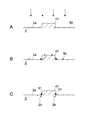
- the formation method of the first resin material 51 is not particularly limited, and typically, a liquid, gaseous or mist organic material is formed on the substrate surface 2a by an appropriate coating method such as a spraying method, a spin coating method, or an evaporation method. To be applied. 4A to 4C schematically show a method of forming the first resin material 51.
- a vaporized mist-like organic material 5a is supplied to the surface 2a of the substrate 2.
- the substrate 2 is maintained at a temperature below room temperature, for example.
- the mist-like organic material 5a condenses into droplet-like organic material 5b on the substrate surface 2a as shown in FIG. 4B.
- the droplet-like organic material 5b enters a fine gap due to a capillary phenomenon, or moves on the substrate 2 while being dropped or aggregated by its own surface tension. As shown in FIG.
- the material layer 41 is unevenly distributed at the boundary 2b between the side surface 41s of the material layer 41 and the surface 2a of the substrate 2. Then, the 1st resin material 51 is formed in the boundary part 2b by hardening the said organic material.
- the first resin material 51 may be provided continuously around the first inorganic material layer 41 along the boundary 2b, or may be provided intermittently around the first inorganic material layer 41. Also good. The coverage with respect to the device layer 3 can be improved by providing the 1st resin material 51 continuously along the boundary part 2b.
- the first resin material 51 is formed from the droplet-shaped organic material 5b, the side surface 41s of the first inorganic material layer 41 and the surface 2a of the substrate 2 at the boundary 2b The resin material easily penetrates into the narrow gap G (FIG. 3) in which the angle formed by is less than 90 °. Thereby, the gap G of the boundary portion 2b is filled with the first resin material 51, and a high water vapor barrier property for the device layer 3 can be obtained.
- the organic material constituting the first resin material 51 is not particularly limited.
- the first inorganic material is formed into droplets on the substrate 2 by its own surface tension, aggregates, moves on the substrate, and moves to the first inorganic material.
- a material that can be unevenly distributed around the layer 41 is used.
- an acrylic resin is used, and more specifically, an acrylic ultraviolet curable resin is used. Thereby, the organic material unevenly distributed in the boundary part 2b can be hardened easily.
- the second inorganic material layer 42 covering the surface 41a and the side surface 41s of the first inorganic material layer 41 is formed on the surface 2a of the substrate 2.
- the second inorganic material layer 42 is laminated on the surface 41a in the surface 41a of the first inorganic material layer 41, and the side surfaces of the first resin material 51 and the first inorganic material layer 41 in the boundary portion 2b. Laminated on 41s.
- the first inorganic material layer 41 is made of the same material as the second inorganic material layer 42 and is in contact with the second inorganic material layer 42. Adhesion with is improved.
- the organic material (resin material) after curing is not limited to those unevenly distributed in the boundary portion 2b.
- the organic material is present on the substrate surface 2a other than the boundary portion 2b, the surface 41a of the first inorganic material layer 41, or the like. It may remain.
- the second inorganic material layer 42 has a region laminated on the first inorganic material layer 41 via the second resin material 52 as shown in FIG.
- the second resin material 52 is interposed between the first inorganic material layer 41 and the second inorganic material layer 42, and the surface of the first inorganic material layer 41 is independent of the first resin material 51. 41a is unevenly distributed. Even in this case, since the adhesion between the first inorganic material layer 41 and the second inorganic material layer 42 can be maintained, the barrier characteristics of the element structure 10 are not impaired.
- the element structure 10 of the present embodiment since the side surface of the device layer 3 is covered with the first inorganic material layer 41 and the second inorganic material layer 42, And oxygen can be prevented from entering.
- the fall of the barrier characteristic accompanying the coverage defect of the 1st inorganic material layer 41 or the 2nd inorganic material layer 42 is carried out. And stable device characteristics can be maintained over a long period of time.
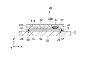
- FIG. 6 is a cross-sectional view schematically showing a configuration of an element structure according to the second exemplary embodiment of the present invention.
- configurations different from those of the first embodiment will be mainly described, and configurations similar to those of the above-described embodiment will be denoted by the same reference numerals, and description thereof will be omitted or simplified.
- the element structure 20 of the present embodiment further includes a second resin material 52 interposed between the first inorganic material layer 41 and the second inorganic material layer 42.
- the second resin material 52 is unevenly distributed on the surface of the first inorganic material layer 41 independently of the first resin material 51.
- the surface of the first inorganic material layer 41 is not necessarily flat.
- the particles P are in the film before film formation (when the substrate is transported or before being loaded into the film formation apparatus) or during film formation. In some cases, unevenness may be formed by mixing in the surface. If particles are mixed into the first inorganic material layer 41, the coverage of the first inorganic material layer 41 with respect to the device layer 3 may be reduced, and the desired barrier characteristics may not be obtained.
- the element structure 20 has a structure in which the second resin material 52 is filled in a poorly coated portion of the first inorganic material layer 41 caused by mixing of particles P or the like.
- the second resin material 52 is unevenly distributed at the boundary portion 32b between the surface of the first inorganic material layer 41 and the peripheral surface of the particles P.
- the coverage of the device layer 3 is enhanced, and the second inorganic material layer 42 can be appropriately formed by the second resin material 52 functioning as a base.
- the second resin material 52 is formed by the same method as the first resin material 51.
- the second resin material 52 may be made of the same organic material as the first resin material 51.
- the first resin material 51 and the second resin material 52 can be simultaneously formed in the same process.
- the first resin material 51 is formed by aggregation of the droplet-shaped organic material on the boundary portion 2b
- the second resin material 52 is formed by aggregation of the droplet-shaped organic material on the boundary portion 32b. Is done.
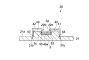
- FIG. 7 is a schematic cross-sectional view showing an element structure according to the third embodiment.
- configurations different from those of the first embodiment will be mainly described, and configurations similar to those of the above-described embodiment will be denoted by the same reference numerals, and description thereof will be omitted or simplified.
- the element structure 30 of the present embodiment includes a substrate 21 having the device layer 3, a convex portion 40 that covers the side surface 3 s of the device layer 3, and a surface of the substrate 21 that covers the convex portion 40 and the device layer 3.
- the first inorganic material layer 41 and the second inorganic material layer 42 are formed.
- the convex portion 40 is formed on the surface 21 a of the substrate 21, and has a concave portion 40 a that accommodates the device layer 3 in the central portion.
- the bottom surface of the recess 40a is formed at a position higher than the surface 21a of the substrate 21, but may be formed at the same height as the surface 21a or at a position lower than the surface 21a. May be.
- the element structure 30 further includes a resin material 53 (first resin material) interposed between the first inorganic material layer 41 and the second inorganic material layer 42.
- the resin material 53 is unevenly distributed on the boundary portion 21 b between the outer side surface of the convex portion 40 and the surface 21 a of the substrate 21, and the boundary portion 22 b between the inner side surface of the convex portion 40 and the device layer 3. Thereby, the coating defect of the 1st and 2nd inorganic material layers 41 and 42 with respect to the convex part 40 and the surface 3a of the device layer 3 can be suppressed, and the improvement of a barrier characteristic can be aimed at.
- the resin material 53 is formed by the same method as the first and second resin materials 51 and 52 described above, and the resin material 53 is unevenly distributed in the above-described portions by using the surface tension of the droplet-shaped organic material. Can do.
- the second inorganic material layer 42 covering the first inorganic material layer 41 is configured as a single layer, but the second inorganic material layer 42 may be configured as a multilayer film.
- an organic material may be supplied onto the substrate for each layer deposition to form a resin material that is unevenly distributed on the concavo-convex portion of the substrate, whereby the barrier property can be further improved.
- the first resin material 51 is unevenly distributed around the inorganic material layer 41 after the formation of the first inorganic material layer 41, but before the formation of the first inorganic material layer 41, the device The first resin material 51 may be unevenly distributed around the layer 3. Thereby, the covering efficiency of the device layer 3 by the first inorganic material layer 41 can be increased.
Landscapes
- Physics & Mathematics (AREA)
- Optics & Photonics (AREA)
- Engineering & Computer Science (AREA)
- Manufacturing & Machinery (AREA)
- Chemical & Material Sciences (AREA)
- Materials Engineering (AREA)
- Electroluminescent Light Sources (AREA)
Abstract
Description
上記基体は、第1の面と、上記第1の面とは反対側の第2の面とを有する。
上記デバイス層は、上記第1及び第2の面のうち少なくとも上記第1の面に配置される。
上記凸部は、上記第1の面に形成される。
上記第1の樹脂材は、上記凸部の周囲に偏在する。
上記基板の表面に液状の有機材料が供給され、上記凸部の側面と上記基板の表面との境界部に前記有機材料が凝集させられる。
上記基板の表面に、上記凸部及び上記有機材料を被覆する第2の無機材料層が形成される。
上記基体は、第1の面と、上記第1の面とは反対側の第2の面とを有する。
上記デバイス層は、上記第1及び第2の面のうち少なくとも上記第1の面に配置される。
上記凸部は、上記第1の面に形成される。
上記第1の樹脂材は、上記凸部の周囲に偏在する。
第1の無機材料層の表面は必ずしも平坦ではなく、例えば成膜時においてパーティクル等が膜中に混入することで凹凸が形成される場合がある。第1の無機材料層にパーティクルが混入すると、デバイス層に対する第1の無機材料層のカバレッジ性が低下し所期のバリア特性が得られなくなるおそれがある。
そのため上記素子構造体は、パーティクルの混入等により生じた第1の無機材料層の被覆不良部に第2の樹脂材が充填された構造を有する。典型的には、第1の樹脂材は、第1の無機材料層の表面とパーティクルの周面との境界部に偏在する。これにより、デバイス層の被覆性が高まるとともに、第2の樹脂材が下地として機能することで第2の無機材料層の適正な成膜が可能となる。
上記基板の表面に液状の有機材料が供給され、上記凸部の側面と上記基板の表面との境界部に前記有機材料が凝集させられる。
上記基板の表面に、上記凸部及び上記有機材料を被覆する第2の無機材料層が形成される。
図1は、本発明の一実施形態に係る素子構造体を示す概略断面図であり、図2はその平面図である。各図においてX軸、Y軸及びZ軸方向は相互に直交する3軸方向を示しており、本実施形態ではX軸及びY軸方向は相互に直交する水平方向、Z軸方向は鉛直方向を示している。
図6は、本発明の第2の実施形態に係る素子構造体の構成を模式的に示す断面図である。以下、第1の実施形態と異なる構成について主に説明し、上述の実施形態と同様の構成については同様の符号を付しその説明を省略または簡略化する。
図7は、第3の実施形態に係る素子構造体を示す概略断面図である。以下、第1の実施形態と異なる構成について主に説明し、上述の実施形態と同様の構成については同様の符号を付しその説明を省略または簡略化する。
2b,21b,22b,32b…境界部
3…デバイス層
10,20,30…素子構造体
40…凸部
41…第1の無機材料層
42…第2の無機材料層
51,53…第1の樹脂材
52…第2の樹脂材
Claims (10)
- 第1の面と、前記第1の面とは反対側の第2の面とを有する基体と、
前記第1及び第2の面のうち少なくとも前記第1の面に配置されるデバイス層と、
前記第1の面に形成される凸部と、
前記凸部の周囲に偏在する第1の樹脂材と
を具備する素子構造体。 - 請求項1に記載の素子構造体であって、
前記凸部は、前記デバイス層を被覆する第1の無機材料層で構成され、
前記素子構造体は、前記第1の樹脂材と前記第1の無機材料層とを被覆する第2の無機材料層をさらに具備する
素子構造体。 - 請求項2に記載の素子構造体であって、
前記第1の無機材料層と前記第2の無機材料層との間に介在し、前記第1の樹脂材とは独立して前記凸部の表面に偏在する第2の樹脂材をさらに具備する
素子構造体。 - 請求項2に記載の素子構造体であって、
前記凸部の表面と前記凸部の表面に付着したパーティクルとの境界部を充填する第2の樹脂材をさらに具備する
素子構造体。 - 請求項1から4のいずれか1項に記載の素子構造体であって、
前記第1の樹脂材は、前記凸部の側面と前記第1の面との境界部に沿って連続的に設けられる
素子構造体。 - 請求項5に記載の素子構造体であって、
前記境界部における前記凸部の側面と前記第1の面とのなす角は90°未満であり、
前記境界部は、前記第1の樹脂材で充填される
素子構造体。 - 請求項1から6のいずれか1項に記載の素子構造体であって、
前記第1の無機材料層は、シリコン化合物で構成される
素子構造体。 - 請求項1から7のいずれか1項に記載の素子構造体であって、
前記第1の樹脂材は、アクリル樹脂及びポリウレア樹脂のいずれかで構成される
素子構造体。 - 請求項1から8のいずれか1項に記載の素子構造体であって、
前記デバイス層は、有機発光層を含む
素子構造体。 - 基板の表面に設けられたデバイス層を被覆する第1の無機材料層で構成された凸部を形成し、
前記基板の表面に液状の有機材料を供給し、前記凸部の側面と前記基板の表面との境界部に前記有機材料を凝集させ、
前記基板の表面に、前記凸部及び前記有機材料を被覆する第2の無機材料層を形成する
素子構造体の製造方法。
Priority Applications (4)
| Application Number | Priority Date | Filing Date | Title |
|---|---|---|---|
| CN201480032156.6A CN105284186B (zh) | 2013-06-07 | 2014-05-21 | 元件结构体及其制造方法 |
| US14/896,572 US10276827B2 (en) | 2013-06-07 | 2014-05-21 | Device structure and method of producing the same |
| JP2015521279A JP6282647B2 (ja) | 2013-06-07 | 2014-05-21 | 素子構造体及びその製造方法 |
| KR1020157032612A KR101685869B1 (ko) | 2013-06-07 | 2014-05-21 | 소자 구조체 및 그 제조 방법 |
Applications Claiming Priority (2)
| Application Number | Priority Date | Filing Date | Title |
|---|---|---|---|
| JP2013-120814 | 2013-06-07 | ||
| JP2013120814 | 2013-06-07 |
Publications (1)
| Publication Number | Publication Date |
|---|---|
| WO2014196137A1 true WO2014196137A1 (ja) | 2014-12-11 |
Family
ID=52007798
Family Applications (1)
| Application Number | Title | Priority Date | Filing Date |
|---|---|---|---|
| PCT/JP2014/002661 Ceased WO2014196137A1 (ja) | 2013-06-07 | 2014-05-21 | 素子構造体及びその製造方法 |
Country Status (6)
| Country | Link |
|---|---|
| US (1) | US10276827B2 (ja) |
| JP (1) | JP6282647B2 (ja) |
| KR (1) | KR101685869B1 (ja) |
| CN (1) | CN105284186B (ja) |
| TW (1) | TWI600190B (ja) |
| WO (1) | WO2014196137A1 (ja) |
Cited By (25)
| Publication number | Priority date | Publication date | Assignee | Title |
|---|---|---|---|---|
| JP2016181373A (ja) * | 2015-03-24 | 2016-10-13 | パイオニア株式会社 | 発光装置 |
| WO2018142490A1 (ja) * | 2017-01-31 | 2018-08-09 | 堺ディスプレイプロダクト株式会社 | 有機el表示装置およびその製造方法 |
| WO2018155415A1 (ja) * | 2017-02-21 | 2018-08-30 | 株式会社アルバック | 成膜方法、成膜装置、素子構造体の製造方法、及び素子構造体の製造装置 |
| WO2018155419A1 (ja) * | 2017-02-21 | 2018-08-30 | 株式会社アルバック | 気化器および素子構造体の製造装置 |
| WO2018155425A1 (ja) * | 2017-02-21 | 2018-08-30 | 株式会社アルバック | 素子構造体の製造方法 |
| JP2018147883A (ja) * | 2018-03-05 | 2018-09-20 | 堺ディスプレイプロダクト株式会社 | 有機elデバイスの製造方法および成膜装置 |
| JP2019003929A (ja) * | 2018-03-28 | 2019-01-10 | 堺ディスプレイプロダクト株式会社 | 薄膜封止構造形成装置 |
| JP6469936B1 (ja) * | 2017-03-16 | 2019-02-13 | 堺ディスプレイプロダクト株式会社 | 有機elデバイスの製造方法、成膜方法および成膜装置 |
| US10276837B2 (en) | 2017-06-27 | 2019-04-30 | Sakai Display Products Corporation | Method for producing organic electroluminescent device |
| US10276830B2 (en) | 2017-03-30 | 2019-04-30 | Sakai Display Products Corporation | Organic electroluminescent device and method for producing same |
| WO2019130431A1 (ja) * | 2017-12-26 | 2019-07-04 | 堺ディスプレイプロダクト株式会社 | 有機el表示装置およびその製造方法 |
| US10516136B2 (en) | 2017-06-13 | 2019-12-24 | Sakai Display Products Corporation | Multilayer thin film encapsulation structure for a organic electroluminescent device |
| US10522784B2 (en) | 2017-03-08 | 2019-12-31 | Sakai Display Products Corporation | Method for producing organic electroluminescent device and film deposition apparatus |
| US10581028B2 (en) | 2017-11-29 | 2020-03-03 | Sakai Display Products Corporation | Method for producing organic electroluminescent display device |
| US10637003B2 (en) | 2017-11-29 | 2020-04-28 | Sakai Display Products Corporation | Organic electroluminescent display device and method for producing same |
| US10644256B2 (en) | 2017-12-25 | 2020-05-05 | Sakai Display Products Corporation | Organic electroluminescent display device and method for producing same |
| US10693104B2 (en) | 2017-12-26 | 2020-06-23 | Sakai Display Products Corporation | Organic electroluminescent device and method for producing same |
| US10734599B2 (en) | 2016-06-30 | 2020-08-04 | Hon Hai Precision Industry Co., Ltd. | Organic EL display device and method for manufacturing same |
| US10897027B2 (en) | 2017-07-13 | 2021-01-19 | Sakai Display Products Corporation | Organic electroluminescent display device and method for producing same |
| US10950682B2 (en) | 2017-11-29 | 2021-03-16 | Sakai Display Products Corporation | Method for manufacturing organic electroluminescent device |
| US11075249B2 (en) | 2018-01-31 | 2021-07-27 | Sakai Display Products Corporation | Method for producing organic electroluminescent display device comprising polydiacetylene layers |
| US11088348B2 (en) | 2018-01-31 | 2021-08-10 | Sakai Display Products Corporation | Method for producing organic electroluminescent display device comprising polydiacetylene layer |
| US11107876B2 (en) | 2018-04-26 | 2021-08-31 | Sakai Display Products Corporation | Organic electroluminescent device and method for producing same |
| US11825683B2 (en) | 2018-04-20 | 2023-11-21 | Sakai Display Products Corporation | Organic electroluminescent device including thin film encapsulation structure and method for producing same |
| US11950488B2 (en) | 2018-04-20 | 2024-04-02 | Sakai Display Products Corporation | Organic electroluminescent device and method for producing same |
Families Citing this family (2)
| Publication number | Priority date | Publication date | Assignee | Title |
|---|---|---|---|---|
| US10823355B2 (en) * | 2016-01-27 | 2020-11-03 | Lite-On Electronics (Guangzhou) Limited | Light-emitting module for vehicle lamp |
| CN106505139A (zh) * | 2016-09-18 | 2017-03-15 | 深圳市核高基科技有限公司 | 微显示器件封装结构和工艺 |
Citations (7)
| Publication number | Priority date | Publication date | Assignee | Title |
|---|---|---|---|---|
| JP2004079291A (ja) * | 2002-08-13 | 2004-03-11 | Matsushita Electric Works Ltd | 有機電界発光素子 |
| JP2005100685A (ja) * | 2003-09-22 | 2005-04-14 | Toshiba Matsushita Display Technology Co Ltd | 表示装置及び表示装置の製造方法 |
| JP2006222071A (ja) * | 2005-01-17 | 2006-08-24 | Seiko Epson Corp | 発光装置、発光装置の製造方法、及び電子機器 |
| JP2006222070A (ja) * | 2005-01-17 | 2006-08-24 | Seiko Epson Corp | 発光装置、発光装置の製造方法、及び電子機器 |
| JP2007287660A (ja) * | 2006-03-22 | 2007-11-01 | Canon Inc | 有機発光装置 |
| JP2007311219A (ja) * | 2006-05-19 | 2007-11-29 | Tokki Corp | 有機エレクトロルミネッセンス素子 |
| JP2013016372A (ja) * | 2011-07-05 | 2013-01-24 | Seiko Epson Corp | 電気光学装置及び電子機器 |
Family Cites Families (6)
| Publication number | Priority date | Publication date | Assignee | Title |
|---|---|---|---|---|
| JP4032909B2 (ja) * | 2002-10-01 | 2008-01-16 | ソニー株式会社 | 有機発光表示装置の製造方法 |
| JP2005123012A (ja) * | 2003-10-16 | 2005-05-12 | Pioneer Electronic Corp | 有機エレクトロルミネセンス表示パネルとその製造方法 |
| CN100495762C (zh) * | 2005-01-17 | 2009-06-03 | 精工爱普生株式会社 | 发光装置、发光装置的制造方法、以及电子设备 |
| JP2007042616A (ja) * | 2005-06-29 | 2007-02-15 | Asahi Kasei Corp | 発光素子及び表示デバイス並びにそれらの製造方法 |
| JP5211265B2 (ja) | 2010-06-23 | 2013-06-12 | 東京エレクトロン株式会社 | 封止膜形成方法、封止膜形成装置 |
| JP2013073880A (ja) | 2011-09-29 | 2013-04-22 | Ulvac Japan Ltd | 発光素子の製造方法 |
-
2014
- 2014-05-21 JP JP2015521279A patent/JP6282647B2/ja active Active
- 2014-05-21 KR KR1020157032612A patent/KR101685869B1/ko active Active
- 2014-05-21 US US14/896,572 patent/US10276827B2/en active Active
- 2014-05-21 CN CN201480032156.6A patent/CN105284186B/zh active Active
- 2014-05-21 WO PCT/JP2014/002661 patent/WO2014196137A1/ja not_active Ceased
- 2014-05-30 TW TW103118990A patent/TWI600190B/zh active
Patent Citations (7)
| Publication number | Priority date | Publication date | Assignee | Title |
|---|---|---|---|---|
| JP2004079291A (ja) * | 2002-08-13 | 2004-03-11 | Matsushita Electric Works Ltd | 有機電界発光素子 |
| JP2005100685A (ja) * | 2003-09-22 | 2005-04-14 | Toshiba Matsushita Display Technology Co Ltd | 表示装置及び表示装置の製造方法 |
| JP2006222071A (ja) * | 2005-01-17 | 2006-08-24 | Seiko Epson Corp | 発光装置、発光装置の製造方法、及び電子機器 |
| JP2006222070A (ja) * | 2005-01-17 | 2006-08-24 | Seiko Epson Corp | 発光装置、発光装置の製造方法、及び電子機器 |
| JP2007287660A (ja) * | 2006-03-22 | 2007-11-01 | Canon Inc | 有機発光装置 |
| JP2007311219A (ja) * | 2006-05-19 | 2007-11-29 | Tokki Corp | 有機エレクトロルミネッセンス素子 |
| JP2013016372A (ja) * | 2011-07-05 | 2013-01-24 | Seiko Epson Corp | 電気光学装置及び電子機器 |
Cited By (48)
| Publication number | Priority date | Publication date | Assignee | Title |
|---|---|---|---|---|
| JP2016181373A (ja) * | 2015-03-24 | 2016-10-13 | パイオニア株式会社 | 発光装置 |
| US10734599B2 (en) | 2016-06-30 | 2020-08-04 | Hon Hai Precision Industry Co., Ltd. | Organic EL display device and method for manufacturing same |
| US11165043B2 (en) | 2017-01-31 | 2021-11-02 | Sakai Display Products Corporation | Organic electroluminescent display device and method for producing same |
| WO2018142490A1 (ja) * | 2017-01-31 | 2018-08-09 | 堺ディスプレイプロダクト株式会社 | 有機el表示装置およびその製造方法 |
| US10720603B2 (en) | 2017-01-31 | 2020-07-21 | Sakai Display Products Corporation | Organic electroluminescent display device and method for producing same |
| JPWO2018142490A1 (ja) * | 2017-01-31 | 2019-02-14 | 堺ディスプレイプロダクト株式会社 | 有機el表示装置およびその製造方法 |
| JPWO2018155419A1 (ja) * | 2017-02-21 | 2019-06-27 | 株式会社アルバック | 気化器および素子構造体の製造装置 |
| JPWO2018155415A1 (ja) * | 2017-02-21 | 2019-11-07 | 株式会社アルバック | 成膜方法、成膜装置、素子構造体の製造方法、及び素子構造体の製造装置 |
| WO2018155415A1 (ja) * | 2017-02-21 | 2018-08-30 | 株式会社アルバック | 成膜方法、成膜装置、素子構造体の製造方法、及び素子構造体の製造装置 |
| WO2018155419A1 (ja) * | 2017-02-21 | 2018-08-30 | 株式会社アルバック | 気化器および素子構造体の製造装置 |
| TWI690106B (zh) * | 2017-02-21 | 2020-04-01 | 日商愛發科股份有限公司 | 元件結構體之製造方法 |
| KR20190062564A (ko) | 2017-02-21 | 2019-06-05 | 가부시키가이샤 아루박 | 기화기 및 소자 구조체의 제조 장치 |
| WO2018155425A1 (ja) * | 2017-02-21 | 2018-08-30 | 株式会社アルバック | 素子構造体の製造方法 |
| CN110268091B (zh) * | 2017-02-21 | 2021-10-12 | 株式会社爱发科 | 成膜方法、成膜装置、元件结构体的制造方法及元件结构体的制造装置 |
| CN110268091A (zh) * | 2017-02-21 | 2019-09-20 | 株式会社爱发科 | 成膜方法、成膜装置、元件结构体的制造方法及元件结构体的制造装置 |
| US10522784B2 (en) | 2017-03-08 | 2019-12-31 | Sakai Display Products Corporation | Method for producing organic electroluminescent device and film deposition apparatus |
| US10665817B2 (en) | 2017-03-08 | 2020-05-26 | Sakai Display Products Corporation | Method for producing organic electroluminescent device and film deposition apparatus |
| JP6469936B1 (ja) * | 2017-03-16 | 2019-02-13 | 堺ディスプレイプロダクト株式会社 | 有機elデバイスの製造方法、成膜方法および成膜装置 |
| US10741800B2 (en) | 2017-03-16 | 2020-08-11 | Sakai Display Products Corporation | Method for manufacturing organic el device, including a thin film encapsulation structure film-forming method, and film-forming apparatus for the same |
| US10505150B2 (en) | 2017-03-30 | 2019-12-10 | Sakai Display Products Corporation | Organic electroluminescent device and method for producing same |
| US10276830B2 (en) | 2017-03-30 | 2019-04-30 | Sakai Display Products Corporation | Organic electroluminescent device and method for producing same |
| US10516136B2 (en) | 2017-06-13 | 2019-12-24 | Sakai Display Products Corporation | Multilayer thin film encapsulation structure for a organic electroluminescent device |
| US10847748B2 (en) | 2017-06-13 | 2020-11-24 | Sakai Display Products Corporation | Multilayer thin film encapsulation structure for an organic electroluminescent device |
| US10461284B2 (en) | 2017-06-27 | 2019-10-29 | Sakai Display Products Corporation | Method for producing organic electroluminescent device |
| US10276837B2 (en) | 2017-06-27 | 2019-04-30 | Sakai Display Products Corporation | Method for producing organic electroluminescent device |
| US10897027B2 (en) | 2017-07-13 | 2021-01-19 | Sakai Display Products Corporation | Organic electroluminescent display device and method for producing same |
| US11513643B2 (en) | 2017-07-13 | 2022-11-29 | Sakai Display Products Corporation | Organic electroluminescent display device and method for producing same |
| US10637009B1 (en) | 2017-11-29 | 2020-04-28 | Sakai Display Products Corporation | Organic electroluminescent display device |
| US10950682B2 (en) | 2017-11-29 | 2021-03-16 | Sakai Display Products Corporation | Method for manufacturing organic electroluminescent device |
| US10637003B2 (en) | 2017-11-29 | 2020-04-28 | Sakai Display Products Corporation | Organic electroluminescent display device and method for producing same |
| US10581028B2 (en) | 2017-11-29 | 2020-03-03 | Sakai Display Products Corporation | Method for producing organic electroluminescent display device |
| US10644256B2 (en) | 2017-12-25 | 2020-05-05 | Sakai Display Products Corporation | Organic electroluminescent display device and method for producing same |
| US11145839B2 (en) | 2017-12-25 | 2021-10-12 | Sakai Display Products Corporation | Organic electroluminescent display device and method for producing same |
| JP6556417B1 (ja) * | 2017-12-26 | 2019-08-07 | 堺ディスプレイプロダクト株式会社 | 有機el表示装置およびその製造方法 |
| US10944074B2 (en) | 2017-12-26 | 2021-03-09 | Sakai Display Products Corporation | Organic electroluminescent display device and method for producing same |
| US11075361B2 (en) | 2017-12-26 | 2021-07-27 | Sakai Display Products Corporation | Organic electroluminescent device and method for producing same |
| US10693104B2 (en) | 2017-12-26 | 2020-06-23 | Sakai Display Products Corporation | Organic electroluminescent device and method for producing same |
| WO2019130431A1 (ja) * | 2017-12-26 | 2019-07-04 | 堺ディスプレイプロダクト株式会社 | 有機el表示装置およびその製造方法 |
| US11812634B2 (en) | 2017-12-26 | 2023-11-07 | Sakai Display Products Corporation | Organic electroluminescent device and method for producing same |
| US11075249B2 (en) | 2018-01-31 | 2021-07-27 | Sakai Display Products Corporation | Method for producing organic electroluminescent display device comprising polydiacetylene layers |
| US11088348B2 (en) | 2018-01-31 | 2021-08-10 | Sakai Display Products Corporation | Method for producing organic electroluminescent display device comprising polydiacetylene layer |
| JP2018147883A (ja) * | 2018-03-05 | 2018-09-20 | 堺ディスプレイプロダクト株式会社 | 有機elデバイスの製造方法および成膜装置 |
| JP2019003929A (ja) * | 2018-03-28 | 2019-01-10 | 堺ディスプレイプロダクト株式会社 | 薄膜封止構造形成装置 |
| US11950488B2 (en) | 2018-04-20 | 2024-04-02 | Sakai Display Products Corporation | Organic electroluminescent device and method for producing same |
| US12402492B2 (en) | 2018-04-20 | 2025-08-26 | Sakai Display Products Corporation | Organic electroluminescent device including thin film encapsulation structure and method for producing same |
| US11825683B2 (en) | 2018-04-20 | 2023-11-21 | Sakai Display Products Corporation | Organic electroluminescent device including thin film encapsulation structure and method for producing same |
| US11107876B2 (en) | 2018-04-26 | 2021-08-31 | Sakai Display Products Corporation | Organic electroluminescent device and method for producing same |
| US11711955B2 (en) | 2018-04-26 | 2023-07-25 | Sakai Display Products Corporation | Organic electroluminescent device with organic flattening layer having surface Ra of 50 nm or less and method for producing same |
Also Published As
| Publication number | Publication date |
|---|---|
| CN105284186A (zh) | 2016-01-27 |
| JP6282647B2 (ja) | 2018-02-21 |
| JPWO2014196137A1 (ja) | 2017-02-23 |
| KR101685869B1 (ko) | 2016-12-12 |
| CN105284186B (zh) | 2017-05-17 |
| TW201501383A (zh) | 2015-01-01 |
| US10276827B2 (en) | 2019-04-30 |
| KR20150143749A (ko) | 2015-12-23 |
| TWI600190B (zh) | 2017-09-21 |
| US20160126495A1 (en) | 2016-05-05 |
Similar Documents
| Publication | Publication Date | Title |
|---|---|---|
| JP6282647B2 (ja) | 素子構造体及びその製造方法 | |
| KR101261142B1 (ko) | 유기 발광 장치, 조명 장치, 표시 장치, 및 유기 발광 장치의 제조 방법 | |
| CN106024834B (zh) | Oled显示面板、显示装置及oled显示面板的制作方法 | |
| TWI420722B (zh) | 具有封裝單元之裝置 | |
| US11018318B2 (en) | Display panel and manufacturing method thereof | |
| CN107565066A (zh) | Oled面板的制作方法及oled面板 | |
| US11316131B2 (en) | OLED display panel having multi-groove retaining walls | |
| CN104538566A (zh) | Oled的封装方法及oled封装结构 | |
| WO2016011709A1 (zh) | 有机发光二极管显示面板及其制造方法 | |
| US9876195B2 (en) | Method for packaging organic light-emitting diode apparatus, organic light-emitting diode packaging apparatus and display device | |
| WO2018157449A1 (zh) | 有机电致发光显示装置及其制作方法 | |
| US9887381B2 (en) | Organic light-emitting display device with adhesive unit and method of manufacturing the same | |
| CN110265571A (zh) | 封装体、显示面板及显示面板的封装方法 | |
| CN106684262A (zh) | 有机发光显示装置及其封装方法 | |
| KR101570852B1 (ko) | 발수층을 구비하는 전자 소자 모듈 | |
| US9425437B2 (en) | Method of manufacturing organic light-emitting diode (OLED) display | |
| KR20150136246A (ko) | 유기 발광 표시 장치 및 그 제조 방법 | |
| US20170162827A1 (en) | Substrate structure | |
| CN109952388A (zh) | 气化器及元件结构体的制造装置 | |
| CN111584760A (zh) | 一种显示面板、显示面板的制备方法及显示装置 | |
| US11765926B2 (en) | Thin film encapsulation structure and method for manufacturing the same | |
| KR101481117B1 (ko) | 가요성 기판 및 이를 이용하는 전기광학소자 | |
| CN109892012B (zh) | 元件结构体的制造方法 | |
| US10017848B2 (en) | Crucible | |
| JP2020181738A (ja) | 有機デバイス及び製造方法 |
Legal Events
| Date | Code | Title | Description |
|---|---|---|---|
| WWE | Wipo information: entry into national phase |
Ref document number: 201480032156.6 Country of ref document: CN |
|
| 121 | Ep: the epo has been informed by wipo that ep was designated in this application |
Ref document number: 14806832 Country of ref document: EP Kind code of ref document: A1 |
|
| ENP | Entry into the national phase |
Ref document number: 20157032612 Country of ref document: KR Kind code of ref document: A |
|
| ENP | Entry into the national phase |
Ref document number: 2015521279 Country of ref document: JP Kind code of ref document: A |
|
| NENP | Non-entry into the national phase |
Ref country code: DE |
|
| WWE | Wipo information: entry into national phase |
Ref document number: 14896572 Country of ref document: US |
|
| 122 | Ep: pct application non-entry in european phase |
Ref document number: 14806832 Country of ref document: EP Kind code of ref document: A1 |