WO2014188953A1 - 半導体リレー - Google Patents
半導体リレー Download PDFInfo
- Publication number
- WO2014188953A1 WO2014188953A1 PCT/JP2014/062950 JP2014062950W WO2014188953A1 WO 2014188953 A1 WO2014188953 A1 WO 2014188953A1 JP 2014062950 W JP2014062950 W JP 2014062950W WO 2014188953 A1 WO2014188953 A1 WO 2014188953A1
- Authority
- WO
- WIPO (PCT)
- Prior art keywords
- case
- circuit board
- semiconductor relay
- central axis
- semiconductor
- Prior art date
- Legal status (The legal status is an assumption and is not a legal conclusion. Google has not performed a legal analysis and makes no representation as to the accuracy of the status listed.)
- Ceased
Links
Images






Classifications
-
- H—ELECTRICITY
- H05—ELECTRIC TECHNIQUES NOT OTHERWISE PROVIDED FOR
- H05K—PRINTED CIRCUITS; CASINGS OR CONSTRUCTIONAL DETAILS OF ELECTRIC APPARATUS; MANUFACTURE OF ASSEMBLAGES OF ELECTRICAL COMPONENTS
- H05K7/00—Constructional details common to different types of electric apparatus
- H05K7/20—Modifications to facilitate cooling, ventilating, or heating
- H05K7/20845—Modifications to facilitate cooling, ventilating, or heating for automotive electronic casings
- H05K7/20854—Heat transfer by conduction from internal heat source to heat radiating structure
Definitions
- the present invention relates to a semiconductor relay.
- This application claims priority based on Japanese Patent Application No. 2013-109000 filed in Japan on May 23, 2013 and Japanese Patent Application No. 2014-17129 filed in Japan on January 31, 2014. , The contents of which are incorporated herein.
- a semiconductor relay is known as an alternative to a so-called mechanical relay such as an electromagnetic relay.
- the semiconductor relay for example, a bottomed rectangular case whose opening is rectangular, a circuit board on which a semiconductor element provided in the case is mounted, and the opening of the case are closed, Some have a base that supports the circuit board, and a plurality of lead terminals that are provided on the base and electrically connect the circuit board and the mounted body.
- the circuit board includes an input circuit including a light emitting diode through which an input signal is energized, and an output circuit that outputs an output signal in accordance with the input signal input to the input circuit. Further, the circuit board is supported at a substantially central portion of the base and is disposed at a substantially central portion of the case. Further, the plurality of lead terminals are arranged in two rows along the longitudinal direction of the base. Each lead terminal and the circuit board are electrically connected to each other via a connection terminal (see, for example, Patent Document 1).
- the circuit board is arranged at the substantially central portion of the case, although the balance is good, the distance between the semiconductor element and the case is increased and the heat dissipation is improved. It becomes difficult. Further, since the case is formed in a simple bottomed rectangular box shape, it is difficult to reduce the size of the case. As a result, there is a limit to miniaturization of the semiconductor relay. Further, since the plurality of lead terminals are arranged in two rows along the longitudinal direction of the base, it is necessary to perform desired wiring on the mounted body side to which the semiconductor relay is attached, and the occupied area for attaching the semiconductor relay is large growing.
- the present invention provides a semiconductor relay that can be reduced in size and can save installation space.
- a semiconductor relay includes a bottomed cylindrical case, a base portion that can be engaged with an opening of the case, and a case in which the semiconductor switching element is mounted.
- a circuit board provided on the base portion, and a plurality of terminals for electrically connecting the circuit board and the mounted body, and a part of the outer surface of the peripheral wall of the case, A heat dissipating part for dissipating heat was provided, and the circuit board was arranged along the peripheral wall on the opposite side of the center axis of the case from the heat dissipating part.
- the heat dissipation of the case can be enhanced by providing the heat dissipation part in the case. Furthermore, the installation area of the heat radiating part in the case can be increased as much as possible by arranging the circuit board close to the side opposite to the heat radiating part. For this reason, a case can be reduced in size efficiently and, as a result, a semiconductor relay can be reduced in size.
- the case has a bottomed rectangular tube shape so that a cross section in a direction orthogonal to the central axis is substantially square. Formed in the case so as to straddle the bottom surface of the case and one side of the peripheral wall, and a plurality of radiating fins are provided in the cut portion. The cut portion and the heat radiating fin were configured as the heat radiating portion.
- the heat radiating portion can be formed as large as possible without increasing the size of the case. For this reason, a case can be reduced more efficiently.
- the cut portion is located on the opposite side of the peripheral axis from the circuit board in the peripheral wall. It is formed from the approximate center of one side in the direction of the central axis to the vicinity of the place where the central axis passes on the bottom surface.
- the excision part is the circuit board with respect to the central axis of the peripheral wall. It is an inclined surface formed so as to straddle between the substantially center of one side located on the opposite side in the central axis direction and the vicinity of the portion of the bottom surface through which the central axis passes.
- the case in the semiconductor relay according to any one of the first to fourth aspects of the present invention, is made of a material having high thermal conductivity together with the heat radiating portion. It is integrally molded.
- Structuring in this way can further enhance the heat dissipation of the heat dissipation portion, and further reduce the size of the case.
- the plurality of terminals are arranged substantially at the center of the base portion.
- the semiconductor relay can be a relay compliant with ISO-Micro or ISO-Mini (see ISO 7588 for both), and a highly versatile semiconductor relay can be provided. . For this reason, it becomes possible to attach a semiconductor relay directly to a to-be-attached body, and space saving of the installation space of a semiconductor relay can be achieved.
- a signal for PWM controlling the semiconductor switching element is input to the signal line input terminal, and the output terminal Outputs a stepless output signal.
- the drive control of the mounted body can be performed with high precision, and the reliability of the mounted body can be improved and the power can be saved. Moreover, since the heat generation of the semiconductor relay can be suppressed, the heat radiating portion of the case can be reduced in size. As a result, the semiconductor relay can be reduced in size.
- a filler is enclosed in the case.
- This configuration can improve the sealing performance in the case. Moreover, the insulation of the circuit board built in the case can be improved. Furthermore, since the heat generated from the circuit board is efficiently transmitted to the case via the filler, the heat generated from the circuit board can be efficiently dissipated. For this reason, it becomes possible to suppress a case heat dissipation area, and a semiconductor relay can be reduced in size.
- the heat dissipation of a case can be improved by providing a thermal radiation part in a case. Furthermore, the installation area of the heat radiating part in the case can be increased as much as possible by arranging the circuit board close to the side opposite to the heat radiating part. For this reason, a case can be reduced in size efficiently and, as a result, a semiconductor relay can be reduced in size. Further, the semiconductor relay can be a relay compliant with ISO-Micro or ISO-Mini (see ISO 7588), and a highly versatile semiconductor relay can be provided. For this reason, it becomes possible to attach a semiconductor relay directly to a to-be-attached body, and space saving of the installation space of a semiconductor relay can be achieved.
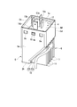
- FIG. 1 is an exploded perspective view of the semiconductor relay 1
- FIG. 2 is a perspective view of the semiconductor relay 1
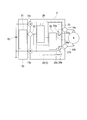
- FIG. 3 is a block diagram of the semiconductor relay 1.
- the semiconductor relay 1 is electrically connected to an electronic control unit (ECU) 60 as an attached body.
- the ECU 60 is mounted on a vehicle, for example, and includes a drive driver 61 for driving a fan motor M for cooling the engine.
- the ECU 60 also has a protection function against overvoltage, overcurrent, overheating, etc. to the semiconductor relay 1.
- the semiconductor relay 1 includes a bottomed cylindrical case 2, a circuit board 3 housed in the case 2, a base portion 4 that can engage with an opening 2 a of the case 2 and close a part thereof, and a base portion 4 is provided with a plurality of terminals 12, 13a, 13b, 14a, 14b for electrically connecting the circuit board 3 and the ECU 60.
- the semiconductor relay 1 is fixed to the vehicle body with the bottom 2b of the case 2 facing downward in the vertical direction.
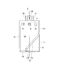
- FIG. 4 is a side view of the semiconductor relay 1.
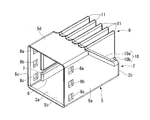
- FIG. 5 is a perspective view of the case 2.
- the case 2 is made of an aluminum material having high thermal conductivity and is formed into a bottomed cylindrical shape by a die-casting method.
- the cylindrical portion 5 of the case 2 is formed so that a cross section in a direction orthogonal to the central axis C is substantially square. That is, the cylinder part 5 is comprised from four side sides, the 1st side edge 5a, the 2nd side edge 5b, the 3rd side edge 5c, and the 4th side edge 5d.
- the first side 5a and the third side 5c are opposed to each other across the central axis C.
- the second side 5b and the fourth side 5d face each other across the central axis C.
- the second side edge 5b and the fourth side edge 5d are orthogonal to the first side edge 5a and the third side edge 5c.
- thick portions 6 are formed on the inner surfaces of the first side 5a and the third side 5c.
- the thick portion 6 is formed from the bottom 2b of the case 2 to slightly before the opening 2a.
- a substrate support groove 7 is formed in the thick portion 6 along the central axis C direction. Further, the substrate support groove 7 is formed closer to the second side 5b than the central axis C.
- the board support groove 7 has a guide function when the circuit board 3 is assembled, and the circuit board 3 is guided and inserted. When the circuit board 3 is inserted to the innermost part of the board support groove 7, the circuit board 3 is positioned and supported by the case 2.
- three holes 8a, 8b, 8c are formed in the first side 5a and the third side 5c, respectively, along the circumferential direction on the opening 2a side of the thick portion 6.
- the hole 8b formed at the center is used for snap fitting fixing the engaging protrusion 15 of the base portion 4 to the case 2, as will be described later.
- the holes 8a and 8c formed on both sides of the hole 8b are engaged with an engagement member provided on the attached body side in order to fix the case 2 to the attached body (not shown). It has become.
- a heat radiating portion 9 is integrally formed on a part of the outer surface of the case 2.
- the heat radiating portion 9 is constituted by a cut portion 10 formed by cutting a part of the case 2 and a plurality of (five in the first embodiment) heat radiating fins 11 integrally formed on the cut portion 10. Yes.
- the cut portion 10 has an inclined surface 10a formed obliquely from the approximate center of the fourth side 5d in the central axis C direction toward the bottom portion 2b, and a direction perpendicular to the bottom portion 2b from the tip of the inclined surface 10a.
- the vertical surface 10b is bent and extended.
- the vertical surface 10b is disposed on the second side 5b side, that is, on the side where the substrate support groove 7 is formed, from the position through which the central axis C of the bottom 2b passes. Moreover, the surface area of the vertical surface 10b is very small with respect to the surface area of the inclined surface 10a. That is, the vertical surface 10b and the inclined surface 10a are connected in the vicinity of the bottom 2b.
- a plurality of heat radiation fins 11 are integrally formed on the inclined surface 10a and the vertical surface 10b thus formed.
- Each radiating fin 11 is in a state of being erected so as to extend in the same direction as the extending direction of the first side 5a and the third side 5c, and the first side 5a and the third side. It is in the state arrange
- the radiation fin 11 is formed in the range which fits in area
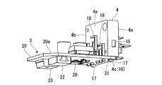
- FIG. 6 is a perspective view in which the base portion 4 and the circuit board 3 are assembled
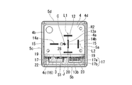
- FIG. 7 is a plan view of the semiconductor relay 1 as viewed from the opening 2 a side of the case 2.
- the base portion 4 is formed in a rectangular parallelepiped shape so as to engage with the opening 2 a of the case 2 and close a part thereof. More specifically, the base 4 is surrounded by the first side 5 a, the fourth side 5 d, and the third side 5 c in the opening 2 a of the case 2, and is more central than the substrate support groove 7. It is formed so as to close the region R2 on the axis C side. That is, in a state where the base portion 4 is attached to the case 2, a gap S ⁇ b> 1 is formed between the base portion 4 and the second side 5 b of the case 2.
- a plurality of terminals 12, 13 a, 13 b, 14 a, and 14 b are erected on the base portion 4 toward the side opposite to the case 2.
- Each of the terminals 12, 13a, 13b, 14a, 14b is formed in a plate shape and is arranged so as to comply with ISO-Mini.
- the signal line input terminal 12 is disposed at the center.
- the signal line input terminal 12 is a member that is electrically connected to the drive driver 61 and that inputs a drive signal output from the drive driver 61 to the semiconductor relay 1.
- a power supply terminal 13a and a GND terminal 13b forming a pair of power supply terminals are arranged on the second side 5b side of the case 2 so as to be on the same line including the signal line input terminal 12.
- the power supply terminal 13a is arranged so that the first side edge 5a and the third side edge 5c face each other in the thickness direction
- the GND terminal 13b is arranged in the thickness direction of the second side edge 5b and the fourth side edge 5d. It arrange
- the power supply terminal 13a and the GND terminal 13b are electrically connected to the battery 62 via the ECU 60.
- Output terminals 14a and 14b are arranged on the first side 5a and third side 5c sides of the case 2 with the power supply terminal 13a interposed therebetween. That is, the output terminals 14a and 14b are arranged along a line L2 orthogonal to the line L1 connecting the GND terminal 13b and the signal line input terminal 12. Among the output terminals 14a and 14b, one output terminal 14a is arranged so that the second side edge 5b and the fourth side edge 5d face the plate thickness direction surface, and the other output terminal 14b is the first output terminal 14b. It arrange
- the output terminals 14 a and 14 b are electrically connected to the fan motor M, and output predetermined power to the fan motor M based on an output signal from the drive driver 61.
- the terminals 12, 13 a, 13 b, 14 a, and 14 b arranged in this way are fixed to the base portion 4 so as to penetrate the base portion 4, as shown in detail in FIG.
- a portion exposed to the end surface on the 2 side is a plurality of bus bars 18.
- Each bus bar 18 is formed to bend along the other surface 4e of the base portion 4 (on the surface opposite to the surface 4d from which the terminals 12 to 14b protrude). And the front-end
- the circuit board 3 is electrically connected to the protruding ends of the bus bars 18.
- the side surface 4 a on the first side 5 a side and the side surface 4 b on the third side 5 c side of the base portion 4 have three holes 8 a, 8 b, 8 c, respectively.
- An engagement projection 15 is integrally formed at a position corresponding to the hole 8b formed in the center of the two.
- the engaging protrusion 15 is inserted into the hole 8 a when the base portion 4 is attached to the opening 2 a of the case 2 to engage the case 2 and the base portion 4. Then, the base portion 4 can be snap-fit fixed to the case 2. Further, since the engaging protrusion 15 has an inclined surface 15a formed on the case 2 side and has a tapered shape, the engaging protrusion 15 is caught by the case 2 when the base portion 4 is fitted into the case 2. The engagement protrusion 15 can be smoothly guided to the hole 8a. For this reason, the base part 4 can be snap-fitted and fixed to the case 2 easily.
- the side surface 4c on the second side 5b side of the base portion 4 is a board mounting surface 16 to which the circuit board 3 is mounted.
- Two engaging claws 17 that engage with the circuit board 3 are integrally formed at both ends in the longitudinal direction of the board mounting surface 16.
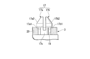
- FIG. 8 is a cross-sectional view of the engaging claw 17.
- each engaging claw 17 is composed of a pair of tongue piece claws 17a and 17b.
- Each tongue claw 17a, 17b includes support portions 17a1, 17b1 rising from the side surface 4c of the base portion 4, claw body 17a2, 17b2 integrally formed at the tip of each support portion 17a1, 17b1, and support portions 17a1, 17b1. It is comprised by the support
- Each of the support portions 17a1 and 17b1 is configured to be elastically deformable in a perspective direction by a space formed between the support portions 17a1 and 17b1, and is snap-fit fixed to an engagement hole 19 formed in the circuit board 3.
- the claw portion main bodies 17a2 and 17b2 are configured to prevent the circuit board 3 from dropping off from the support portions 17a1 and 17b1 in a state where the support portions 17a1 and 17b1 are inserted into engagement holes 19 described later of the circuit board 3. It is configured as a locking means.
- Each tongue claw 17a, 17b is formed so as to taper toward the tip, and is easily inserted into the engagement hole 19 of the circuit board 3.
- an engaging claw 17 for mechanically fixing the base portion 4 and the circuit board 3 is formed on the side surface 4c of the base portion 4 on the second side 5b side, while each of the terminals 12 to 14b.
- the front end of the bus bar 18 for electrically connecting the circuit board 3 and the circuit board 3 is slightly outside the corner portion between the one surface 4e of the base portion 4 and the side surface 4c on the second side 5b side of the base portion 4 ( It projects to the lower side in FIG. In this way, the engaging claws 17 and the tips of the bus bars 18 are in close proximity to each other.
- the circuit board 3 includes a glass epoxy board 20 having a substantially rectangular shape in plan view.
- the glass epoxy substrate 20 is guided and inserted into the substrate support groove 7 formed in the case 2.
- a flattened portion 20a is formed at the end of the glass epoxy substrate 20 on the insertion side into the case 2, and the glass epoxy substrate 20 can be prevented from being misassembled into the case 2 by improving visibility.
- the end portion of the glass epoxy substrate 20 on the base portion 4 side constitutes a base attachment portion 21 attached to the substrate attachment surface 16 of the base portion 4.
- Two engagement holes 19 are formed in a portion of the base mounting portion 21 corresponding to the engagement claws 17.
- substrate 20 comprises the bus-bar attachment part 21a in the position adjacent to the base attachment part 21.
- FIG. A plurality (five in this first embodiment) of bus bar insertion holes 19a are formed at positions corresponding to the tips of the bus bars 18 in the bus bar mounting portion 21a.
- the bus bar insertion hole 19a is formed in a substantially rectangular shape so as to correspond to the cross-sectional shape of the tip of the bus bar 18, and the circuit pattern on the glass epoxy board 20 is electrically conductive so as to surround the bus bar insertion hole 19a. Is provided. And the front-end
- a half-bridge IC 23 and a logic IC 28 are mounted on the glass epoxy substrate 20.
- the half bridge IC 23 is configured by connecting two semiconductor switching elements 24a and 24b between power supply terminals 13a and 13b to which a battery 62 is electrically connected, and connecting a pre-driver 25 to each of the semiconductor switching elements 24a and 24b. Circuit.
- the choke coil 22 removes noise on the circuit.
- Each of the semiconductor switching elements 24a and 24b has a configuration in which FETs (Field Effect Transistors) 26a and 26b and free-wheeling diodes 27a and 27b are connected in parallel.
- the pre-driver 25 drives the FETs 26 a and 26 b based on the output signal from the drive driver 61.
- the FET 26a and the freewheeling diode 27a of the semiconductor switching element 24a disposed on the positive electrode side (Hi side) of the battery 62 are respectively connected to the Hi side FET 26a
- the FET 26b and the free wheeling diode 27b of the semiconductor switching element 24b arranged on the negative electrode side (Lo side) of the battery 62 are referred to as the Hi-side free-wheeling diode 27a, and are referred to as the Lo-side FET 26b and the Lo-side free-wheeling diode 27b, respectively.
- the logic IC 28 is electrically connected to the ECU 60 through the signal line input terminal 12 and is connected to the pre-driver 25 of the half bridge IC 23.
- the logic IC 28 converts the output signal from the drive driver 61 of the ECU 60 into a signal that enables the half bridge IC 23 to be driven.
- the low frequency PWM signal output from the drive driver 61 is converted into a high frequency PWM signal and output to the half bridge IC 23.
- the fan motor M is connected to both sides of the Hi-side semiconductor switching element 24a.
- the engaging claw 17 of the base part 4 to which the plurality of terminals 12, 13 a, 13 b, 14 a, 14 b are fixed is inserted into the engaging hole 19 of the circuit board 3 on which each electronic component is mounted.
- the circuit board 3 is fixed by snap fit.
- the plurality of bus bars 18 are electrically connected to predetermined connection portions on the circuit board 3.
- the end opposite to the base portion 4 of the circuit board 3 is directed toward the opening 2a of the case 2, and the positions of the engagement protrusion 15 of the base portion 4 and the hole 8b of the case 2 are aligned.
- the circuit board 3 is inserted into the case 2 so as to be guided by the board support groove 7 of the case 2.
- the filler J (see FIG. 7) is injected from the gap S1 between the base portion 4 and the second side 5b of the case 2. Thereby, the assembly of the semiconductor relay 1 is completed.
- the assembled semiconductor relay 1 is fixed to the vehicle body with the bottom 2b of the case 2 facing downward in the vertical direction, that is, with the heat dissipating part 9 of the case 2 facing downward in the vertical direction.
- a material having high flame retardancy and high thermal conductivity such as a material mainly composed of an epoxy resin or a material mainly composed of a silicone-modified polymer.
- FIG. 9A is an operation explanatory diagram of the semiconductor relay 1 and shows a current flowing through the semiconductor relay 1.
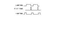
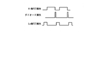
- FIG. 9B is an operation explanatory diagram of the semiconductor relay 1 and shows a timing chart of power loss of the Hi-side FET 29a, the Lo-side FET 29b, and the Hi-side return diode 27a.
- the FET 26a of the Hi-side semiconductor switching element 24a is OFF, and the FET 26b of the Lo-side semiconductor switching element 24b is ON.
- the drive current Id flows through the fan motor M.
- the Lo-side FET 26b is turned OFF. At this time, an electromotive force is generated due to the fact that the drive current Id does not flow through the fan motor M. For this reason, by turning on the Hi-side FET 26a, a closed circuit is formed between the Hi-side FET 26a and the fan motor M, and an induced current Iy generated by the electromotive force is passed through the closed circuit.
- the Hi-side FET 26a when the Hi-side FET 26a is turned on, it takes a little time after the Lo-side FET 26b is turned off so that the Hi-side FET 26a and the Lo-side FET 26b are not turned on at the same time.
- the Hi-side FET 26a is turned on with an interval. For this reason, while the Lo-side FET 26b is turned off and the Hi-side FET 26a is turned on, the induced current Iy 'flows through the Hi-side freewheeling diode 27a, and power loss occurs in the freewheeling diode 27a.
- power loss occurs in the high-side free-wheeling diode 27a only for a short time from when the Lo-side FET 26b is turned off to when the Hi-side FET 26a is turned on.
- the time from when the Lo-side FET 26b is turned off to when the Hi-side FET 26a is turned on is set to about several microseconds, for example.
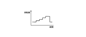
- FIG. 10 is a graph showing changes in the rotational speed of the fan motor M when the vertical axis represents the rotational speed of the fan motor M and the horizontal axis represents time.
- the semiconductor relay 1 when driving the fan motor M, the semiconductor relay 1 can be controlled not only by ON / OFF control but also by PWM (pulse width modulation) control.
- PWM pulse width modulation
- a signal for performing PWM control is output from the drive driver 61 of the ECU 60, and a signal is input to the half bridge IC 23 via the logic IC 28 of the semiconductor relay 1. Then, by outputting a stepless output signal from the half bridge IC 23, the fan motor M can be driven at a desired rotational speed.
- the signal input terminal 12 falls to the GND level.
- the ECU 60 detects that the signal input terminal 12 has dropped to the GND level, it determines that the half-bridge IC 23 has failed.
- the circuit board 3 is driven as described above, heat is generated due to power loss of the free-wheeling diodes 27a and 27b. This heat is transmitted to the case 2 via the circuit board 3 and the filler J filled in the case 2, and is radiated from the case 2.
- the entire case 2 is formed by aluminum die casting having high thermal conductivity, and is formed so that a cross section in a direction orthogonal to the central axis C of the cylindrical portion 5 is substantially square.
- the heat of the circuit board 3 is dissipated.
- the case 2 is compared with the case 2 that is simply formed in a bottomed rectangular tube shape. The surface area of is increased. For this reason, the heat dissipation of the case 2 is improved accordingly.
- the cut portion 10 includes an inclined surface 10a and a vertical surface 10b that is bent and extended along the direction perpendicular to the bottom 2b from the end of the inclined surface 10a on the bottom 2b side. For this reason, an updraft passes along the cutting part 10 without stagnation, and the heat dissipation of the thermal radiation part 9 further improves (refer the arrow in FIG. 2).
- the substrate support groove 7 formed in the case 2 is formed closer to the second side 5b than the central axis C (see FIGS. 4 and 5). That is, the circuit board 3 is arranged closer to the second side 5b than the central axis C.
- the heat radiation part 9 can be formed as large as possible between the vicinity of the central axis C of the case 2 and the fourth side 5d. Therefore, the heat radiation area of the case 2 can be increased as much as possible, and the case 2 can be reliably downsized.
- the bottom portion 2b is fixed to the vehicle body in a state where the bottom portion 2b is directed upward in the vertical direction, similarly, the heat of the circuit board 3 can be efficiently radiated from the entire case 2.
- the circuit board 3 is not arranged at the center of the case 2 as in the prior art and is arranged closer to the second side 5b than the central axis C, the circuit board 3 is also arranged on the second side 5b. Heat is easily transmitted, and the heat of the circuit board 3 can be radiated more efficiently.
- the case 2 is filled with the filler J, the heat from the circuit board 3 can be more efficiently transferred to the case 2. Further, by filling the case 2 with the filler J, the sealing property in the case 2 can be enhanced and the insulation property of the circuit board 3 can be enhanced.
- the filler J serves as a buffering agent, reducing the load applied to the electrical connection between the terminals 12 to 14b and the circuit board 3 due to the external impact. Or damage to the circuit board 3 can be prevented.
- a substrate support groove 7 is formed on the inner surface of the case 2, and the semiconductor relay 1 is assembled by inserting the circuit board 3 into the substrate support groove 7. For this reason, the circuit board 3 can be reliably fixed in the case 2 without the circuit board 3 rattling. In addition, since the substrate support groove 7 functions as a guide for guiding the circuit board 3 into the case 2, the assembly property of the circuit board 3 can be improved.
- the signal line input terminal 12 is disposed at the approximate center of the base portion 4, and the power supply terminals 13 a and 13 b are disposed on both sides of the signal line input terminal 12. Further, output terminals 14a and 14b are arranged along a line L2 orthogonal to the line L1 connecting the power supply terminals 13a and 13b.
- the semiconductor relay 1 having high versatility can be obtained. For this reason, it becomes possible to attach the semiconductor relay 1 directly in the relay box electrically connected to the ECU 60 or the like, and the space for mounting the semiconductor relay 1 can be saved.
- two semiconductor switching elements 24a and 24b are mounted on the circuit board 3 of the semiconductor relay 1 so as to be connected between the positive and negative electrodes of the battery 62 (between the power supply terminals 13a and 13b).
- the fan motor M is connected to both sides of the two semiconductor switching elements 24a and 24b with the Hi-side semiconductor switching element 24a interposed therebetween.
- the Lo-side FET 26b is turned OFF, and then the Hi-side FET 26a is turned ON, whereby the power loss of the Hi-side return diode 27a can be minimized. That is, this power loss can be made sufficiently smaller than the power loss of the freewheeling diode in the conventional semiconductor relay. For this reason, the heat generated when the semiconductor relay 1 is driven can be suppressed. Therefore, the case 2 can be further downsized, and as a result, the semiconductor relay 1 can be miniaturized as much as possible.
- the semiconductor relay 1 when driving the fan motor M, the semiconductor relay 1 can be controlled by PWM (pulse width modulation).
- PWM pulse width modulation
- the rotation speed of the fan motor M can be easily changed, and the heat generated from the circuit board 3 can be further reduced. For this reason, it becomes possible to miniaturize the semiconductor relay 1 more reliably.
- the drive control of the fan motor M can be performed with high accuracy.
- the engaging claw 17 is integrally formed on the side surface 4 c of the base portion 4, and the engaging claw 17 and the circuit board 3 are snap-fit fixed. Can be easily positioned, and the base portion 4 and the circuit board 3 can be easily and reliably fixed. Furthermore, an engagement claw 17 for mechanically fixing the base portion 4 and the circuit board 3 and a front end of each bus bar 18 for electrically connecting each of the terminals 12 to 14b and the circuit board 3, They are arranged close to each other. That is, the strength of the electrical connection portion between each of the terminals 12 to 14b and the circuit board 3 can be mechanically assisted by the engaging claw 17 at a position close to the electrical connection portion. For this reason, it is possible to prevent the electrical connection between the terminals 12 to 14b and the circuit board 3 from being broken due to vibration or the like.
- the present invention is not limited to the above-described embodiment, and includes various modifications made to the above-described embodiment without departing from the spirit of the present invention.
- the semiconductor relay 1 is applied to the drive driver 61 for driving the fan motor M for cooling the engine mounted on the vehicle.
- the present invention is not limited to this, and the semiconductor relay 1 can be used for various electric devices.
- the plurality of terminals 12, 13a, 13b, 14a, 14b of the semiconductor relay 1 can be arranged as follows.
- the output terminals 14a and 14b are disposed so that the first side 5a and the third side 5c of the case 2 face the plate thickness direction surface along the line L2 orthogonal to the line L1 connecting the power terminals 13a and 13b. Has been placed.
- the fan motor M is connected to both sides of the two semiconductor switching elements 24a and 24b of the circuit board 3 with the Hi-side semiconductor switching element 24a interposed therebetween.
- the present invention is not limited to this, and the fan motor M may be connected to the circuit board 3 as follows.
- FIGSecond modification of the first embodiment 12A and 12B are operation explanatory diagrams of the second modification of the semiconductor relay 1.
- 12A shows a current flowing through the semiconductor relay 1
- FIG. 12B shows a timing chart of power loss of the Hi-side FET 29a, the Lo-side FET 29b, and the Hi-side return diode 27a.
- the fan motor M is connected to both sides of the two semiconductor switching elements 24a and 24b of the circuit board 3 with the Lo-side semiconductor switching element 24b interposed therebetween.
- the FET 26a of the Hi-side semiconductor switching element 24a is turned on, and the FET 26b of the Lo-side semiconductor switching element 24b is turned off.
- the drive current Id flows through the fan motor M.
- the Hi-side FET 26a is turned off.
- the Lo-side FET 26b is turned on with a slight time interval after the Hi-side FET 26a is turned off so that the Hi-side FET 26a and the Lo-side FET 26b are not turned on simultaneously.
- a closed circuit is formed between the Lo-side FET 26b and the fan motor M, and an induced current Iy generated by the electromotive force flows through the closed circuit.
- the Hi-side FET 26a is turned off and the Lo-side FET 26b is turned on, the induced current Iy ′ flows through the Lo-side freewheeling diode 27b, and a slight power loss occurs in the freewheeling diode 27b.
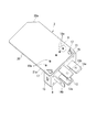
- FIG. 13 is a perspective view in which the base portion 4 and the circuit board 3 are assembled in the second embodiment
- FIG. 14 is an enlarged view of a portion A in FIG.
- the same reference numerals are given to the same aspects as those in the first embodiment, and the description thereof is omitted.
- the difference between the first embodiment and the second embodiment described above is that the connection state between the front end of the bus bar 18 and the circuit board 3 is different.
- a press-fit connection portion 18 a is integrally formed at the tip of each bus bar 18.
- a substantially circular bus bar insertion hole 39a into which the press-fit connecting portion 18a can be press-fitted is formed in the glass epoxy board 20, and the glass epoxy board 20 is formed on the inner peripheral surface of the bus bar insertion hole 39a.
- a conductive portion connected to the circuit pattern arranged above is provided. Then, by press-fitting the press-fit connection portion 18a into the bus bar insertion hole 39a of the glass epoxy substrate 20, the glass epoxy substrate 20 and the bus bar 18 are press-fit connected, and electrical connection is also performed at the same time.
- the press-fit connection means that the circuit board 3 and the bus bar 18 are electrically connected by the repulsive force of the press-fit connection part 18a after the press-fit connection part 18a is press-fitted into the bus bar insertion hole 39a.
- the circuit board 3 and the bus bar 18 can be more easily connected.
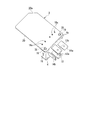
- FIGS. 15A and 15B are perspective views in which the base portion 4 and the circuit board 3 are assembled, and show a connection process between the base portion 4 and the circuit board 3, respectively.
- the difference between the second embodiment and the third embodiment described above is that, in the second embodiment, the fixing of the base portion 4 and the circuit board 3 is the same as in the first embodiment.
- the base portion 4 and the circuit board 3 are fixed by heat caulking.
- a protrusion 35 that can be inserted into the engagement hole 19 is integrally formed on the side surface 4 c of the base portion 4 at a position corresponding to the engagement hole 19 of the glass epoxy substrate 20.
- the base portion 4 is attached so that the protrusions 35 are inserted into the engagement holes 19 of the glass epoxy substrate 20 (FIG. 15A). reference).
- the tip of the projection 35 protruding through the engagement hole 19 of the glass epoxy substrate 20 is heated to melt the tip of the projection 35 (see FIG. 15B).
- the melted portion 35 a formed by melting the tip of the projection 35 functions as a locking means for preventing the base portion 4 from falling off the glass epoxy substrate 20.
- the protrusion 35 (melting portion 35a) and the base portion 4 and the circuit board 3 are in close contact with each other.
- the backlash of the base part 4 can be prevented. For this reason, the electrical connection between the bus bar 18 and the circuit board 3 can be more reliably stabilized.
- the heat dissipation of the case can be enhanced by providing the heat dissipation portion in the case. Furthermore, the installation area of the heat radiating part in the case can be increased as much as possible by arranging the circuit board close to the side opposite to the heat radiating part. For this reason, a case can be reduced in size efficiently and, as a result, a semiconductor relay can be reduced in size. Further, the semiconductor relay can be a relay compliant with ISO-Micro or ISO-Mini (see ISO 7588), and a highly versatile semiconductor relay can be provided. For this reason, it becomes possible to attach a semiconductor relay directly to a to-be-attached body, and space saving of the installation space of a semiconductor relay can be achieved.
Landscapes
- Physics & Mathematics (AREA)
- Thermal Sciences (AREA)
- Engineering & Computer Science (AREA)
- Microelectronics & Electronic Packaging (AREA)
- Cooling Or The Like Of Electrical Apparatus (AREA)
- Electronic Switches (AREA)
- Connection Or Junction Boxes (AREA)
Abstract
有底筒状のケース(2)と、このケース(2)の開口部(2a)に係合可能なベース部(4)と、ケース(2)に内装され、半導体スイッチング素子が実装されている回路基板(3)と、ベース部(4)に設けられ、回路基板(3)と被取付体とを電気的に接続するための複数の端子(12),(13a),(13b),(14a),(14b)と、を備え、ケース(2)の筒部(5)一部に、このケース(2)の熱を放熱するための放熱部(9)を設け、ケース(2)の中心軸に対して放熱部(9)とは反対側に、筒部(5)の側壁に沿うように回路基板(3)を配置した。
Description
本発明は、半導体リレーに関するものである。
本願は、2013年5月23日に、日本に出願された特願2013-109000号、および2014年1月31日に、日本に出願された特願2014-17129号に基づき優先権を主張し、その内容をここに援用する。
本願は、2013年5月23日に、日本に出願された特願2013-109000号、および2014年1月31日に、日本に出願された特願2014-17129号に基づき優先権を主張し、その内容をここに援用する。
従来から、電磁リレー等のいわゆるメカリレーの代替として、半導体リレーが知られている。半導体リレーとしては、例えば、開口部が長方形状になっている有底長四角形状のケースと、このケース内に設けられた半導体素子が実装される回路基板と、ケースの開口部を閉塞し、回路基板を支持するベースと、ベースに設けられ回路基板と被取付体とを電気的に接続するための複数のリード端子と、を備えたものがある。
回路基板は、入力信号が通電される発光ダイオードを含む入力回路、及びその入力回路に入力される入力信号に応じて出力信号を出力する出力回路を備えている。また、回路基板は、ベースの略中央部に支持されると共に、ケースの略中央部に配置される。さらに、複数のリード端子は、ベースの長手方向に沿って2列に配置されている。そして、各リード端子と回路基板とが、各々接続端子を介して電気的に接続されている(例えば、特許文献1参照)。
しかしながら、上述の従来技術にあっては、ケースの略中央部に回路基板が配置されているので、バランス的には良いものの、半導体素子とケースとの距離が離れてしまい放熱性を向上させることが困難となる。また、ケースが単純な有底長四角形状の箱型に形成されているので、ケースを小型化しにくい。この結果、半導体リレーの小型化に限界がある。
また、複数のリード端子がベースの長手方向に沿って2列に配置されているので、半導体リレーが取り付けられる被取付体側で所望の配線を行う必要があり、半導体リレーを取り付けるための占有面積が大きくなる。
また、複数のリード端子がベースの長手方向に沿って2列に配置されているので、半導体リレーが取り付けられる被取付体側で所望の配線を行う必要があり、半導体リレーを取り付けるための占有面積が大きくなる。
本発明は、小型化ができ、且つ取付けスペースの省スペース化を図ることができる半導体リレーを提供する。
本発明の第一の態様によれば、半導体リレーは、有底筒状のケースと、このケースの開口部に係合可能なベース部と、前記ケースに内装され、半導体スイッチング素子が実装されている回路基板と、前記ベース部に設けられ、前記回路基板と被取付体とを電気的に接続するための複数の端子と、を備え、前記ケースの周壁における外面の一部に、このケースの熱を放熱するための放熱部を設け、前記ケースの中心軸に対して前記放熱部とは反対側に、前記周壁に沿うように前記回路基板を配置した。
このように、ケースに放熱部を設けることにより、ケースの放熱性を高めることができる。さらに、回路基板を放熱部とは反対側に寄せて配置することにより、ケースにおける放熱部の設置面積をできる限り大きくすることができる。このため、ケースを効率よく小型化することができ、この結果、半導体リレーを小型化できる。
本発明の第二の態様によれば、本発明の第一の態様に係る半導体リレーにおいて、前記ケースは、前記中心軸と直交する方向の断面が略正方形となるように有底四角筒状に形成されており、前記ケースに、このケースの底面と前記周壁の一辺とに跨るように、前記ケースの一部を切除した切除部を形成し、この切除部に複数の放熱フィンを設け、これら切除部及び放熱フィンを、前記放熱部として構成した。
このように構成することで、ケースを大型化することなく、放熱部をできる限り大きく形成することができる。このため、さらに効率よくケースを小型化することができる。
本発明の第三の態様によれば、本発明の第二の態様に係る半導体リレーにおいて、前記切除部は、前記周壁のうち、前記中心軸に対して前記回路基板とは反対側に位置する一辺の中心軸方向略中央から前記底面の前記中心軸の通る箇所の近傍に至るまで形成されている。
このように構成することで、ケースを効率よく小型化しつつ、放熱部を大きく形成することができる。
本発明の第四の態様によれば、本発明の第二の態様若しくは第三の態様に係る半導体リレーにおいて、前記切除部は、前記周壁のうち、前記中心軸に対して前記回路基板とは反対側に位置する一辺の中心軸方向略中央と、前記底面の前記中心軸の通る箇所の近傍との間に跨るように形成された傾斜面である。
このように構成することで、放熱部を通る空気の流れが良くなり、放熱部による放熱性を高めることができる。このため、さらに、ケースを小型化することが可能になる。
本発明の第五の態様によれば、本発明の第一の態様から第四の態様の何れか一の態様に係る半導体リレーにおいて、前記ケースは、前記放熱部と共に熱伝導性の高い材料により一体成形されている。
このように構成することで、放熱部の放熱性をさらに高めることができ、ケースをさらに小型化することができる。
本発明の第六の態様によれば、本発明の第一の態様から第五の態様の何れか一の態様に係る半導体リレーにおいて、前記複数の端子は、前記ベース部の略中央に配置された信号線入力端子と、この信号線入力端子を含む同一線上に配置された一対の電源端子と、これら一対の電源端子を結ぶ線と直交する線に沿って配置された一対の出力端子と、を備えている。
このように構成することで、半導体リレーを、ISO-MicroやISO-Mini(何れもISO 7588参照)に準拠するリレーとすることができ、汎用性の高い半導体リレーを提供することが可能になる。このため、被取付体に直接半導体リレーを取り付けることが可能になり、半導体リレーの取付スペースの省スペース化を図ることができる。
本発明の第七の態様によれば、本発明の第六の態様に係る半導体リレーにおいて、前記信号線入力端子には、前記半導体スイッチング素子をPWM制御するための信号が入力され、前記出力端子からは、無段階の出力信号が出力される。
このように構成することで、被取付体の駆動制御を精度よく行うことができ、被取付体の信頼性を向上したり、省電力化したりすることが可能になる。また、半導体リレーの発熱を抑えることができるので、ケースの放熱部を小型化できる。この結果、半導体リレーを小型化できる。
本発明の第八の態様によれば、本発明の第一の態様から第七の態様の何れか一の態様に係る半導体リレーにおいて、前記ケース内に充填剤を封入した。
このように構成することで、ケース内のシール性を高めることができる。また、ケースに内装された回路基板の絶縁性を高めることができる。さらに、回路基板から発生する熱が充填剤を介して効率よくケースに伝達されるので、回路基板から発生する熱を効率よく放熱させることができる。このため、ケース放熱面積を抑えることが可能になり、半導体リレーを小型化できる。
上記の半導体リレーによれば、ケースに放熱部を設けることにより、ケースの放熱性を高めることができる。さらに、回路基板を放熱部とは反対側に寄せて配置することにより、ケースにおける放熱部の設置面積をできる限り大きくすることができる。このため、ケースを効率よく小型化することができ、この結果、半導体リレーを小型化できる。
また、半導体リレーを、ISO-MicroやISO-Mini(ISO 7588参照)に準拠するリレーとすることができ、汎用性の高い半導体リレーを提供することが可能になる。このため、被取付体に直接半導体リレーを取り付けることが可能になり、半導体リレーの取付スペースの省スペース化を図ることができる。
また、半導体リレーを、ISO-MicroやISO-Mini(ISO 7588参照)に準拠するリレーとすることができ、汎用性の高い半導体リレーを提供することが可能になる。このため、被取付体に直接半導体リレーを取り付けることが可能になり、半導体リレーの取付スペースの省スペース化を図ることができる。
(第1実施形態)
(半導体リレー)
次に、本発明の第1実施形態を図1~図12Bに基づいて説明する。
図1は、半導体リレー1の分解斜視図、図2は、半導体リレー1の斜視図、図3は、半導体リレー1のブロック図である。
図1~図3に示すように、半導体リレー1は、被取付体としての電子制御ユニット(ECU)60に電気的に接続される。ECU60は、例えば車両に搭載されており、エンジン冷却用のファンモータMを駆動するための駆動ドライバ61を備えている。また、ECU60は、半導体リレー1への過電圧、過電流、過熱等に対する保護機能を有している。
(半導体リレー)
次に、本発明の第1実施形態を図1~図12Bに基づいて説明する。
図1は、半導体リレー1の分解斜視図、図2は、半導体リレー1の斜視図、図3は、半導体リレー1のブロック図である。
図1~図3に示すように、半導体リレー1は、被取付体としての電子制御ユニット(ECU)60に電気的に接続される。ECU60は、例えば車両に搭載されており、エンジン冷却用のファンモータMを駆動するための駆動ドライバ61を備えている。また、ECU60は、半導体リレー1への過電圧、過電流、過熱等に対する保護機能を有している。
半導体リレー1は、有底筒状のケース2と、ケース2に内装されている回路基板3と、ケース2の開口部2aに係合しその一部を閉塞可能なベース部4と、ベース部4に設けられ、回路基板3とECU60とを電気的に接続するための複数の端子12,13a,13b,14a,14bとを備えている。そして、半導体リレー1は、ケース2の底部2bが鉛直方向下側に向く状態で車体に固定される。
(ケース)
図4は、半導体リレー1の側面図である。図5は、ケース2の斜視図である。
図4、図5に示すように、ケース2は、熱伝導性の高いアルミニウム材からなり、ダイキャスト製法により有底筒状に形成されている。ケース2の筒部5は、中心軸Cと直交する方向の断面が略正方形となるように形成されている。すなわち、筒部5は、第1側辺5a、第2側辺5b、第3側辺5c、及び第4側辺5dの4つの側辺から構成される。そして、中心軸Cを挟んで第1側辺5aと第3側辺5cとが互いに対向している。また、中心軸Cを挟んで第2側辺5bと第4側辺5dとが互いに対向している。さらに、第1側辺5a及び第3側辺5cに対し、第2側辺5b及び第4側辺5dが直交した状態になっている。
このような構成のもと、第1側辺5a及び第3側辺5cの内面には、肉厚部6が形成されている。肉厚部6は、ケース2の底部2bから開口部2aのやや手前に至るまで形成されている。
また、肉厚部6には、中心軸C方向に沿って基板支持溝7が形成されている。さらに、基板支持溝7は、中心軸Cよりも第2側辺5b寄りに形成されている。基板支持溝7は、回路基板3の組付け時のガイド機能を備えており、回路基板3がガイドされて挿入される。そして、基板支持溝7の最奥部まで回路基板3が挿入されると、ケース2に回路基板3が位置決め支持される。
また、肉厚部6には、中心軸C方向に沿って基板支持溝7が形成されている。さらに、基板支持溝7は、中心軸Cよりも第2側辺5b寄りに形成されている。基板支持溝7は、回路基板3の組付け時のガイド機能を備えており、回路基板3がガイドされて挿入される。そして、基板支持溝7の最奥部まで回路基板3が挿入されると、ケース2に回路基板3が位置決め支持される。
また、第1側辺5a及び第3側辺5cには、肉厚部6よりも開口部2a側に、それぞれ3つの孔8a,8b,8cが周方向に沿って並んで形成されている。3つの孔8a,8b,8cのうち、中央に形成されている孔8bは、後述するように、ケース2にベース部4の係合突起15をスナップフィット固定するために用いられる。一方、孔8bを挟んで両側に形成されている孔8a,8cは、不図示の被取付体にケース2を固定するために、被取付体側に設けられた係合部材が係合するようになっている。
さらに、ケース2の外面の一部には、放熱部9が一体成形されている。放熱部9は、ケース2の一部を切除してなる切除部10と、この切除部10上に一体成形された複数(この第1実施形態では5つ)の放熱フィン11とにより構成されている。
切除部10は、第4側辺5dの中心軸C方向略中央から底部2bに向かって斜めに形成されている傾斜面10aと、この傾斜面10aの先端から底部2bに直交する方向に沿って屈曲延出されている垂直面10bとにより構成されている。
切除部10は、第4側辺5dの中心軸C方向略中央から底部2bに向かって斜めに形成されている傾斜面10aと、この傾斜面10aの先端から底部2bに直交する方向に沿って屈曲延出されている垂直面10bとにより構成されている。
垂直面10bは、底部2bの中心軸Cが通る位置よりも第2側辺5b側、つまり、基板支持溝7が形成されている側に配置されている。また、垂直面10bの表面積は、傾斜面10aの表面積に対して非常に小さい。すなわち、垂直面10bと傾斜面10aは、底部2bの近傍で接続された状態になっている。
このように形成された傾斜面10a及び垂直面10b上に、複数の放熱フィン11が一体成形されている。各放熱フィン11は、第1側辺5a及び第3側辺5cの延在方向と同じ方向に延在するように立設された状態になっていると共に、第1側辺5aと第3側辺5cとの間に並んで配置された状態になっている。
また、放熱フィン11は、ケース2の切除部10によって切除された領域R1(図4参照)に収まる範囲に形成されている。すなわち、図4に詳示するように、放熱フィン11は、切除部10上にケース2の側面視が長方形状となる範囲で形成されている。
また、放熱フィン11は、ケース2の切除部10によって切除された領域R1(図4参照)に収まる範囲に形成されている。すなわち、図4に詳示するように、放熱フィン11は、切除部10上にケース2の側面視が長方形状となる範囲で形成されている。
(ベース部)
図6は、ベース部4と回路基板3とを組み付けた斜視図、図7は、半導体リレー1をケース2の開口部2a側からみた平面図である。
図1、図6、図7に示すように、ベース部4は、ケース2の開口部2aと係合しその一部を閉塞可能なように、直方体状に形成されている。より具体的には、ベース部4は、ケース2の開口部2aのうち、第1側辺5a、第4側辺5d、及び第3側辺5cにより囲まれ、且つ基板支持溝7よりも中心軸C側の領域R2を閉塞するように形成されている。すなわち、ケース2にベース部4を取り付けた状態では、ベース部4とケース2の第2側辺5bとの間に、隙間S1が形成される。
図6は、ベース部4と回路基板3とを組み付けた斜視図、図7は、半導体リレー1をケース2の開口部2a側からみた平面図である。
図1、図6、図7に示すように、ベース部4は、ケース2の開口部2aと係合しその一部を閉塞可能なように、直方体状に形成されている。より具体的には、ベース部4は、ケース2の開口部2aのうち、第1側辺5a、第4側辺5d、及び第3側辺5cにより囲まれ、且つ基板支持溝7よりも中心軸C側の領域R2を閉塞するように形成されている。すなわち、ケース2にベース部4を取り付けた状態では、ベース部4とケース2の第2側辺5bとの間に、隙間S1が形成される。
また、図7に詳示するように、ベース部4には、ケース2とは反対側に向かって複数の端子12,13a,13b,14a,14bが立設されている。各端子12,13a,13b,14a,14bは、板状に形成されており、ISO-Miniに準拠するように配置されている。
より具体的には、図2、図7に示すように、ベース部4の一面4dの略中央に、ケース2の第1側辺5a及び第3側辺5cと板幅方向面が対向するように信号線入力端子12が配置されている。信号線入力端子12は、駆動ドライバ61に電気的に接続され、この駆動ドライバ61から出力される駆動信号を半導体リレー1に入力するための部材である。
また、信号線入力端子12を含み同一線上となるように、ケース2の第2側辺5b側には、一対の電源端子をなす電源端子13a、GND端子13bが配置されている。さらに、電源端子13aは、第1側辺5a及び第3側辺5cと板厚方向が対向するように配置され、GND端子13bは、第2側辺5b及び第4側辺5dと板厚方向面が対向するように配置されている。電源端子13a,GND端子13bは、ECU60を介してバッテリ62に電気的に接続されている。
また、信号線入力端子12を含み同一線上となるように、ケース2の第2側辺5b側には、一対の電源端子をなす電源端子13a、GND端子13bが配置されている。さらに、電源端子13aは、第1側辺5a及び第3側辺5cと板厚方向が対向するように配置され、GND端子13bは、第2側辺5b及び第4側辺5dと板厚方向面が対向するように配置されている。電源端子13a,GND端子13bは、ECU60を介してバッテリ62に電気的に接続されている。
また、電源端子13aを挟んでケース2の第1側辺5a及び第3側辺5c側には、それぞれ出力端子14a,14bが配置されている。すなわち、出力端子14a,14bは、GND端子13b、信号線入力端子12を結ぶ線L1と直交する線L2に沿って配置されている。
出力端子14a,14bのうち、一方の出力端子14aは、第2側辺5b及び第4側辺5dと板厚方向面が対向するように配置されており、他方の出力端子14bは、第1側辺5a及び第3側辺5cと板厚方向面が対向するように配置されている。出力端子14a,14bは、ファンモータMに電気的に接続されており、駆動ドライバ61からの出力信号に基づいて所定の電力をファンモータMに出力する。
出力端子14a,14bのうち、一方の出力端子14aは、第2側辺5b及び第4側辺5dと板厚方向面が対向するように配置されており、他方の出力端子14bは、第1側辺5a及び第3側辺5cと板厚方向面が対向するように配置されている。出力端子14a,14bは、ファンモータMに電気的に接続されており、駆動ドライバ61からの出力信号に基づいて所定の電力をファンモータMに出力する。
このように配置された各端子12,13a,13b,14a,14bは、図6に詳示するように、ベース部4を貫通する状態でベース部4に固定されており、ベース部4のケース2側の端面に露出する部分は複数のバスバー18となっている。各バスバー18は、ベース部4の他方の一面4e上(端子12~14bが突出している一面4d側と反対の面上)を沿うように屈曲形成されている。そして、各バスバー18の先端は、ベース部4の一面4eとベース部4の第2側辺5b側の側面4cとの間の角部よりもやや外側(図7中下側)に突出した状態になっている。この突出した各バスバー18の先端に、回路基板3が電気的に接続される。
また、図6、図7に詳示するように、ベース部4の第1側辺5a側の側面4aと、第3側辺5c側の側面4bには、それぞれ3つの孔8a,8b,8cのうちの中央に形成されている孔8bに対応する位置に、係合突起15が一体成形されている。
また、図6、図7に詳示するように、ベース部4の第1側辺5a側の側面4aと、第3側辺5c側の側面4bには、それぞれ3つの孔8a,8b,8cのうちの中央に形成されている孔8bに対応する位置に、係合突起15が一体成形されている。
係合突起15は、ケース2の開口部2aにベース部4を取り付ける際、孔8aに挿入されてケース2とベース部4とを係合する。そして、ケース2にベース部4がスナップフィット固定できる。また、係合突起15には、ケース2側に傾斜面15aが形成されて先細り形状になっているので、ケース2内にベース部4を嵌め込む際、ケース2に係合突起15が引っ掛かることがなく、この係合突起15をスムーズに孔8aに導くことができる。このため、ケース2にベース部4を容易にスナップフィット固定できる。
また、ベース部4の第2側辺5b側の側面4cは、回路基板3が取り付けられる基板取付面16である。この基板取付面16の長手方向両端には、回路基板3と係合する2つの係合爪17が一体成形されている。
図8は、係合爪17の断面図である。
図8に詳示するように、各係合爪17は、一対の舌片爪17a,17bにより構成されている。各舌片爪17a,17bは、ベース部4の側面4cから立ち上がる支持部17a1,17b1と、各支持部17a1,17b1の先端に一体成形された爪部本体17a2,17b2と、支持部17a1,17b1の基端部分を連結する支柱部17cにより構成されている。各支持部17a1,17b1は、互いの間に形成された空間によって遠近方向に弾性変形可能に構成されており、回路基板3に形成されている係合孔19にスナップフィット固定される。
図8に詳示するように、各係合爪17は、一対の舌片爪17a,17bにより構成されている。各舌片爪17a,17bは、ベース部4の側面4cから立ち上がる支持部17a1,17b1と、各支持部17a1,17b1の先端に一体成形された爪部本体17a2,17b2と、支持部17a1,17b1の基端部分を連結する支柱部17cにより構成されている。各支持部17a1,17b1は、互いの間に形成された空間によって遠近方向に弾性変形可能に構成されており、回路基板3に形成されている係合孔19にスナップフィット固定される。
すなわち、爪部本体17a2,17b2は、回路基板3の後述する係合孔19に支持部17a1,17b1を挿入した状態で、この支持部17a1,17b1から回路基板3が脱落しないようにするための係止手段として構成されている。また、各舌片爪17a,17bは先端に向かうに従って先細りとなるように形成されており、回路基板3の係合孔19に挿入しやすくなっている。
ここで、ベース部4と回路基板3とを機械的に固定するための係合爪17が、ベース部4の第2側辺5b側の側面4cに形成されている一方、各端子12~14bと回路基板3とを電気的に接続するためのバスバー18の先端が、ベース部4の一面4eとベース部4の第2側辺5b側の側面4cとの間の角部よりもやや外側(図7中下側)に突出されている。このように、係合爪17とバスバー18の先端は、互いに近接配置された状態になっている。
(回路基板)
図1、図3、図6、図7に示すように、回路基板3は平面視略長方形状のガラスエポキシ基板20を有している。このガラスエポキシ基板20がケース2に形成されている基板支持溝7にガイドされて挿入される。ガラスエポキシ基板20のケース2への挿入側の端部には、平面取り部20aが形成されており、視認性を向上させることで、ケース2へのガラスエポキシ基板20の誤組を防止できる。
図1、図3、図6、図7に示すように、回路基板3は平面視略長方形状のガラスエポキシ基板20を有している。このガラスエポキシ基板20がケース2に形成されている基板支持溝7にガイドされて挿入される。ガラスエポキシ基板20のケース2への挿入側の端部には、平面取り部20aが形成されており、視認性を向上させることで、ケース2へのガラスエポキシ基板20の誤組を防止できる。
また、ガラスエポキシ基板20のベース部4側の端部は、ベース部4の基板取付面16に取り付けられるベース取付部21を構成している。このベース取付部21の係合爪17に対応する部位に、2つの係合孔19(図1参照)が形成されている。
さらに、ガラスエポキシ基板20は、ベース取付部21に隣接する位置がバスバー取付部21aを構成している。このバスバー取付部21aにおける各バスバー18の先端に対応する位置に、複数(この第1実施形態では5つ)のバスバー差込孔19aが形成されている。バスバー差込孔19aは、バスバー18の先端の断面形状に対応するように、略長長方形状に形成されており、そのバスバー差込孔19aを囲むよう、ガラスエポキシ基板20上の回路パターンの導電部が設けられている。そして、バスバー差込孔19aに各バスバー18の先端を差込み、はんだ付け等によって回路基板3とバスバー18とを電気的に接続する。
さらに、ガラスエポキシ基板20は、ベース取付部21に隣接する位置がバスバー取付部21aを構成している。このバスバー取付部21aにおける各バスバー18の先端に対応する位置に、複数(この第1実施形態では5つ)のバスバー差込孔19aが形成されている。バスバー差込孔19aは、バスバー18の先端の断面形状に対応するように、略長長方形状に形成されており、そのバスバー差込孔19aを囲むよう、ガラスエポキシ基板20上の回路パターンの導電部が設けられている。そして、バスバー差込孔19aに各バスバー18の先端を差込み、はんだ付け等によって回路基板3とバスバー18とを電気的に接続する。
また、図3、図6に詳示するように、ガラスエポキシ基板20には、ハーフブリッジIC23やロジックIC28が実装されている。ハーフブリッジIC23は、バッテリ62が電気的に接続される電源端子13a,13b間に2つの半導体スイッチング素子24a,24bを接続すると共に、各半導体スイッチング素子24a,24bにプリドライバ25を接続して構成される回路である。尚、チョークコイル22は回路上のノイズを除去する。
各半導体スイッチング素子24a,24bは、それぞれFET(Field effect transistor)26a,26bと、還流ダイオード27a,27bとを並列に接続した構成になっている。プリドライバ25は、駆動ドライバ61からの出力信号に基づいて、FET26a,26bを駆動させる。
尚、以下の説明において、2つの半導体スイッチング素子24a,24bのうち、バッテリ62の正極側(Hi側)に配置されている半導体スイッチング素子24aのFET26a、還流ダイオード27aを、それぞれHi側のFET26a、Hi側の還流ダイオード27aと称し、バッテリ62の負極側(Lo側)に配置されている半導体スイッチング素子24bのFET26b、還流ダイオード27bを、それぞれLo側のFET26b、Lo側の還流ダイオード27bと称して説明する。
尚、以下の説明において、2つの半導体スイッチング素子24a,24bのうち、バッテリ62の正極側(Hi側)に配置されている半導体スイッチング素子24aのFET26a、還流ダイオード27aを、それぞれHi側のFET26a、Hi側の還流ダイオード27aと称し、バッテリ62の負極側(Lo側)に配置されている半導体スイッチング素子24bのFET26b、還流ダイオード27bを、それぞれLo側のFET26b、Lo側の還流ダイオード27bと称して説明する。
ロジックIC28は、信号線入力端子12を介してECU60に電気的に接続されていると共に、ハーフブリッジIC23のプリドライバ25に接続されている。ロジックIC28は、ECU60の駆動ドライバ61からの出力信号をハーフブリッジIC23を駆動可能とする信号に変換する。例えば、駆動ドライバ61から出力された低周波PWM信号を高周波PWM信号に変換してハーフブリッジIC23に出力する。
そして、このように構成された回路基板3の2つの半導体スイッチング素子24a,24bのうち、Hi側の半導体スイッチング素子24aを挟んで両側に、ファンモータMが接続された状態になっている。
そして、このように構成された回路基板3の2つの半導体スイッチング素子24a,24bのうち、Hi側の半導体スイッチング素子24aを挟んで両側に、ファンモータMが接続された状態になっている。
(半導体リレーの組み立て方法)
次に、半導体リレー1の組み立て方法について説明する。
まず、各電子部品が実装された回路基板3の係合孔19に、複数の端子12,13a,13b,14a,14bが固定されたベース部4の係合爪17を挿入し、ベース部4に回路基板3をスナップフィット固定させる。そして、複数のバスバー18を回路基板3上の所定の接続部と電気的に接続する。この状態で回路基板3のベース部4とは反対側端をケース2の開口部2aに向け、さらに、ベース部4の係合突起15とケース2の孔8bとの位置を合わせる。そして、ケース2の基板支持溝7にガイドされるように回路基板3をケース2に差し込む。
次に、半導体リレー1の組み立て方法について説明する。
まず、各電子部品が実装された回路基板3の係合孔19に、複数の端子12,13a,13b,14a,14bが固定されたベース部4の係合爪17を挿入し、ベース部4に回路基板3をスナップフィット固定させる。そして、複数のバスバー18を回路基板3上の所定の接続部と電気的に接続する。この状態で回路基板3のベース部4とは反対側端をケース2の開口部2aに向け、さらに、ベース部4の係合突起15とケース2の孔8bとの位置を合わせる。そして、ケース2の基板支持溝7にガイドされるように回路基板3をケース2に差し込む。
回路基板3をケース2の底部2bまで押し込むと、ケース2の孔8bにベース部4の係合突起15が挿入され、ケース2とベース部4とがスナップフィット固定される。これにより、ケース2内に、回路基板3とベース部4とが収納される。
続いて、ベース部4とケース2の第2側辺5bとの間の隙間S1から充填剤J(図7参照)を注入する。これにより、半導体リレー1の組み立てが完了する。そして、組み立てられた半導体リレー1は、ケース2の底部2bを鉛直方向下側に向けた状態、つまり、ケース2の放熱部9を鉛直方向下側に向けた状態で車体に固定される。
尚、充填剤Jとしては、エポキシ樹脂を主成分としたものや、シリコーン変性ポリマーを主成分としたもの等、難燃性、熱伝導性の高いものを用いることが望ましい。
続いて、ベース部4とケース2の第2側辺5bとの間の隙間S1から充填剤J(図7参照)を注入する。これにより、半導体リレー1の組み立てが完了する。そして、組み立てられた半導体リレー1は、ケース2の底部2bを鉛直方向下側に向けた状態、つまり、ケース2の放熱部9を鉛直方向下側に向けた状態で車体に固定される。
尚、充填剤Jとしては、エポキシ樹脂を主成分としたものや、シリコーン変性ポリマーを主成分としたもの等、難燃性、熱伝導性の高いものを用いることが望ましい。
(半導体リレーの動作)
次に、図9A~図10に基づいて、半導体リレー1の動作について説明する。
図9Aは、半導体リレー1の動作説明図であり、半導体リレー1に流れる電流を示す。図9Bは、半導体リレー1の動作説明図であり、Hi側のFET29a及びLo側のFET29bと、Hi側の還流ダイオード27aの電力損失のタイミングチャートを示す。
図9Aに示すように、ファンモータMを駆動させる場合、Hi側の半導体スイッチング素子24aのFET26aはOFF、Lo側の半導体スイッチング素子24bのFET26bはONになっている。これにより、ファンモータMには、駆動電流Idが流れる。
次に、図9A~図10に基づいて、半導体リレー1の動作について説明する。
図9Aは、半導体リレー1の動作説明図であり、半導体リレー1に流れる電流を示す。図9Bは、半導体リレー1の動作説明図であり、Hi側のFET29a及びLo側のFET29bと、Hi側の還流ダイオード27aの電力損失のタイミングチャートを示す。
図9Aに示すように、ファンモータMを駆動させる場合、Hi側の半導体スイッチング素子24aのFET26aはOFF、Lo側の半導体スイッチング素子24bのFET26bはONになっている。これにより、ファンモータMには、駆動電流Idが流れる。
一方、ファンモータMを停止させる場合、Lo側のFET26bをOFFにする。このとき、ファンモータMに駆動電流Idが流れなくなることに起因する起電力が生じる。このため、Hi側のFET26aをONにすることにより、Hi側のFET26aとファンモータMとの間で閉回路を形成し、この閉回路に、起電力によって生じる誘導電流Iyを流す。
ここで、図9Bに示すように、Hi側のFET26aをONするにあたって、Hi側のFET26aとLo側のFET26bとが同時にON状態とならないように、Lo側のFET26bをOFFにしてから僅かに時間間隔をあけてHi側のFET26aをONにしている。このため、Lo側のFET26bをOFFにしてからHi側のFET26aをONにする間、Hi側の還流ダイオード27aに誘導電流Iy’が流れ、還流ダイオード27aに電力損失が生じる。換言すれば、Lo側のFET26bをOFFにしてからHi側のFET26aをONにするまでの僅かな時間のみ、Hi側の還流ダイオード27aに電力損失が生じる。尚、Lo側のFET26bをOFFにしてからHi側のFET26aをONにするまでの時間は、例えば、数μ秒程度に設定されている。
図10は、縦軸をファンモータMの回転数とし、横軸を時間としたときのファンモータMの回転数の変化を示すグラフである。
同図に示すように、ファンモータMを駆動させるにあたって、半導体リレー1をON/OFF制御するのみならず、PWM(パルス幅変調)制御することも可能である。このPWM制御を行う場合、PWM制御を行うための信号がECU60の駆動ドライバ61から出力され、半導体リレー1のロジックIC28を介してハーフブリッジIC23に信号が入力される。そして、このハーフブリッジIC23から無段階の出力信号が出力されることにより、ファンモータMを所望の回転数で駆動させることができる。
同図に示すように、ファンモータMを駆動させるにあたって、半導体リレー1をON/OFF制御するのみならず、PWM(パルス幅変調)制御することも可能である。このPWM制御を行う場合、PWM制御を行うための信号がECU60の駆動ドライバ61から出力され、半導体リレー1のロジックIC28を介してハーフブリッジIC23に信号が入力される。そして、このハーフブリッジIC23から無段階の出力信号が出力されることにより、ファンモータMを所望の回転数で駆動させることができる。
ここで、ハーフブリッジIC23に過電圧、過電流、過熱等が発生すると、信号入力端子12がGNDレベルまで落ちる。ECU60は、信号入力端子12がGNDレベルまで落ちていることを検出すると、ハーフブリッジIC23が故障していると判断する。
また、上述のように回路基板3を駆動させると還流ダイオード27a,27bの電力損失等により熱が発生する。この熱は、回路基板3を介し、ケース2内に充填されている充填剤Jを介してケース2に伝達され、ケース2から放熱される。
また、上述のように回路基板3を駆動させると還流ダイオード27a,27bの電力損失等により熱が発生する。この熱は、回路基板3を介し、ケース2内に充填されている充填剤Jを介してケース2に伝達され、ケース2から放熱される。
(ケースの放熱作用)
次に、図2、図4に基づいてケース2の放熱作用について説明する。
ケース2は、全体が熱伝導性の高いアルミダイキャストにより形成されており、且つ筒部5の中心軸Cと直交する方向の断面が略正方形となるように形成されているので、ケース2全体から回路基板3の熱が放熱される。これに加え、ケース2には、切除部10と複数の放熱フィン11からなる放熱部9が形成されているので、ケース2を単純に有底四角筒状に形成した場合と比較してケース2の表面積が大きくなっている。このため、この分、ケース2の放熱性が向上している。
次に、図2、図4に基づいてケース2の放熱作用について説明する。
ケース2は、全体が熱伝導性の高いアルミダイキャストにより形成されており、且つ筒部5の中心軸Cと直交する方向の断面が略正方形となるように形成されているので、ケース2全体から回路基板3の熱が放熱される。これに加え、ケース2には、切除部10と複数の放熱フィン11からなる放熱部9が形成されているので、ケース2を単純に有底四角筒状に形成した場合と比較してケース2の表面積が大きくなっている。このため、この分、ケース2の放熱性が向上している。
ここで、ケース2が放熱されることにより、ケース2の周囲に上昇気流が生じる。このとき、半導体リレー1は、ケース2の底部2bを鉛直方向下側に向けた状態で車体に固定された場合には、切除部10にも上昇気流が通過する。切除部10は、傾斜面10aと傾斜面10aの底部2b側の端部からこの底部2bに直交する方向に沿って屈曲延出されている垂直面10bとにより構成されている。このため、切除部10に沿って上昇気流が淀みなく通過し、放熱部9の放熱性がさらに向上する(図2における矢印参照)。
(効果)
したがって、上述の第1実施形態によれば、底部2bを鉛直方向下側に向けた状態で車体に固定した場合、ケース2全体から回路基板3の熱を効率よく放熱することができるので、放熱性を考慮してケース2を大型化する必要がなく、この結果、半導体リレー1を小型化できる。
ここで、ケース2に形成されている基板支持溝7は、中心軸Cよりも第2側辺5b寄りに形成されている(図4、図5参照)。つまり、回路基板3は、中心軸Cよりも第2側辺5b寄りに配置されていることになる。このため、ケース2の中心軸Cの近傍から第4側辺5dに至る間に、放熱部9をできる限り大きく形成することができる。よって、ケース2の放熱面積をできる限り大きくすることができ、ケース2を確実に小型化できる。
尚、底部2bを鉛直方向上側に向けた状態で車体に固定した場合にも、同様に、ケース2全体から回路基板3の熱を効率よく放熱することができる。
また、回路基板3が従来のようにケース2の中央に配置されておらず、中心軸Cよりも第2側辺5b寄りに配置されているので、この第2側辺5bにも回路基板3からの熱が伝達され易くなり、回路基板3の熱をさらに効率よく放熱することができる。
これに加え、ケース2内に充填剤Jが充填されているので、ケース2に回路基板3からの熱をさらに効率よく伝達することができる。また、ケース2内に充填剤Jを充填することにより、ケース2内のシール性を高めることができると共に、回路基板3の絶縁性を高めることができる。
また、例えば半導体リレー1が外部から衝撃を受けた際、充填剤Jが緩衝剤の役割を果たし、外部衝撃によって各端子12~14bと回路基板3との電気的接続部に加わる負荷を軽減したり、回路基板3の損傷を防止したりすることができる。
これに加え、ケース2内に充填剤Jが充填されているので、ケース2に回路基板3からの熱をさらに効率よく伝達することができる。また、ケース2内に充填剤Jを充填することにより、ケース2内のシール性を高めることができると共に、回路基板3の絶縁性を高めることができる。
また、例えば半導体リレー1が外部から衝撃を受けた際、充填剤Jが緩衝剤の役割を果たし、外部衝撃によって各端子12~14bと回路基板3との電気的接続部に加わる負荷を軽減したり、回路基板3の損傷を防止したりすることができる。
さらに、ケース2の内面に基板支持溝7を形成し、この基板支持溝7に回路基板3を差し込むようにして半導体リレー1を組み立てるようになっている。このため、ケース2内で回路基板3がガタツクことなく、回路基板3を確実に固定できる。また、基板支持溝7が、ケース2内へ回路基板3を導くためのガイドとして機能するので、回路基板3の組み付け性を向上させることができる。
そして、ベース部4の略中央に信号線入力端子12が配置され、この信号線入力端子12を挟んで両側に、それぞれ電源端子13a,13bが配置されている。さらに、各電源端子13a,13bを結ぶ線L1と直交する線L2に沿って出力端子14a,14bが配置されている。このように、複数の端子12,13a,13b,14a,14bは、ISO-Miniに準拠するように配置されているので、汎用性の高い半導体リレー1とすることができる。このため、ECU60などに電気的に接続されるリレーボックス内に直接半導体リレー1を取り付けることが可能になり、半導体リレー1の取付スペースの省スペース化を図ることができる。
また、半導体リレー1の回路基板3には、バッテリ62の正負極間(電源端子13a,13b間)に接続されるように2つの半導体スイッチング素子24a,24bが実装されている。そして、2つの半導体スイッチング素子24a,24bのうち、Hi側の半導体スイッチング素子24aを挟んだ両側に、ファンモータMが接続される。このような構成のもと、ファンモータMを停止させるにあたってLo側のFET26bをOFFにした後、Hi側のFET26aをONすることによって、Hi側の還流ダイオード27aの電力損失をできる限り小さくできる。すなわち、従来の半導体リレーにおける還流ダイオードの電力損失と比較して、この電力損失を十分小さくすることができる。このため、半導体リレー1を駆動させた際に発生する熱を抑制することができる。よって、さらにケース2を小型化することができ、この結果、半導体リレー1を極力小型化することができる。
さらに、ファンモータMを駆動させるにあたって、半導体リレー1をPWM(パルス幅変調)制御することができる。このように、PWM制御を行うことによって、ファンモータMの回転数を容易に変化させることができると共に、回路基板3から発生する熱をさらに低減することができる。このため、より確実に半導体リレー1を小型化することが可能になる。また、ファンモータMの駆動制御を精度よく行うことが可能になる。
また、ベース部4の側面4cに係合爪17を一体成形し、この係合爪17と回路基板3とをスナップフィット固定しているので、係合爪17によって、ベース部4と回路基板3との位置決めを容易に行うことができると共に、ベース部4と回路基板3とを容易、且つ確実に固定できる。
さらに、ベース部4と回路基板3とを機械的に固定するための係合爪17と、各端子12~14bと回路基板3とを電気的に接続するための各バスバー18の先端とが、互いに近接配置されている。すなわち、各端子12~14bと回路基板3との電気的接続部の強度を、この電気的接続部に近接した位置において機械的に係合爪17で補助できる。このため、振動等によって各端子12~14bと回路基板3との電気的接続が絶たれてしまうことを防止できる。
さらに、ベース部4と回路基板3とを機械的に固定するための係合爪17と、各端子12~14bと回路基板3とを電気的に接続するための各バスバー18の先端とが、互いに近接配置されている。すなわち、各端子12~14bと回路基板3との電気的接続部の強度を、この電気的接続部に近接した位置において機械的に係合爪17で補助できる。このため、振動等によって各端子12~14bと回路基板3との電気的接続が絶たれてしまうことを防止できる。
尚、本発明は上述の実施形態に限られるものではなく、本発明の趣旨を逸脱しない範囲において、上述の実施形態に種々の変更を加えたものを含む。
例えば、上述の実施形態では、車両に搭載されるエンジン冷却用のファンモータMを駆動するための駆動ドライバ61に半導体リレー1を適用した場合について説明した。しかしながら、これに限られるものではなく、さまざまな電気機器に半導体リレー1を用いることができる。
例えば、上述の実施形態では、車両に搭載されるエンジン冷却用のファンモータMを駆動するための駆動ドライバ61に半導体リレー1を適用した場合について説明した。しかしながら、これに限られるものではなく、さまざまな電気機器に半導体リレー1を用いることができる。
また、半導体リレー1の複数の端子12,13a,13b,14a,14bを以下のように配置することもできる。
(第1実施形態の第1変形例)
上述の第1実施形態では、複数の端子12,13a,13b,14a,14bが、ISO-Miniに準拠するように配置されている場合について説明した。しかしながら、これに限られるものではなく、図11に示すように、複数の端子12,13a,13b,14a,14bを、ISO-Microに準拠するように配置してもよい。このような場合であっても、ベース部4の略中央に信号線入力端子12がケース2の第2側辺5b及び第4側辺5dと板厚方向面が対向するように配置され、この信号線入力端子12を挟んで両側に、それぞれ電源端子13a,13bが並列状に配置されている。さらに、各電源端子13a,13bを結ぶ線L1と直交する線L2に沿って出力端子14a,14bがケース2の第1側辺5a及び第3側辺5cと板厚方向面が対向するように配置されている。
上述の第1実施形態では、複数の端子12,13a,13b,14a,14bが、ISO-Miniに準拠するように配置されている場合について説明した。しかしながら、これに限られるものではなく、図11に示すように、複数の端子12,13a,13b,14a,14bを、ISO-Microに準拠するように配置してもよい。このような場合であっても、ベース部4の略中央に信号線入力端子12がケース2の第2側辺5b及び第4側辺5dと板厚方向面が対向するように配置され、この信号線入力端子12を挟んで両側に、それぞれ電源端子13a,13bが並列状に配置されている。さらに、各電源端子13a,13bを結ぶ線L1と直交する線L2に沿って出力端子14a,14bがケース2の第1側辺5a及び第3側辺5cと板厚方向面が対向するように配置されている。
また、上述の第1実施形態では、回路基板3の2つの半導体スイッチング素子24a,24bのうち、Hi側の半導体スイッチング素子24aを挟んで両側に、ファンモータMが接続された状態になっている。しかしながら、これに限られるものではなく、以下のように、回路基板3にファンモータMを接続してもよい。
(第1実施形態の第2変形例)
図12A、図12Bは、半導体リレー1の第2変形例における動作説明図である。そして、図12Aは、半導体リレー1に流れる電流を示し、図12Bは、Hi側のFET29a及びLo側のFET29bと、Hi側の還流ダイオード27aの電力損失のタイミングチャートを示す。
ここで、図12Aに示すように、ファンモータMは、回路基板3の2つの半導体スイッチング素子24a,24bのうち、Lo側の半導体スイッチング素子24bを挟んで両側に接続されている。
図12A、図12Bは、半導体リレー1の第2変形例における動作説明図である。そして、図12Aは、半導体リレー1に流れる電流を示し、図12Bは、Hi側のFET29a及びLo側のFET29bと、Hi側の還流ダイオード27aの電力損失のタイミングチャートを示す。
ここで、図12Aに示すように、ファンモータMは、回路基板3の2つの半導体スイッチング素子24a,24bのうち、Lo側の半導体スイッチング素子24bを挟んで両側に接続されている。
このような構成のもと、ファンモータMを駆動させる場合、Hi側の半導体スイッチング素子24aのFET26aをONとし、Lo側の半導体スイッチング素子24bのFET26bをOFFとする。これにより、ファンモータMには、駆動電流Idが流れる。
一方、ファンモータMを停止させる場合、Hi側のFET26aをOFFにする。そして、このHi側のFET26aとLo側のFET26bとが同時にON状態とならないように、Hi側のFET26aをOFFにしてから僅かに時間間隔をあけてLo側のFET26bをONにする。
一方、ファンモータMを停止させる場合、Hi側のFET26aをOFFにする。そして、このHi側のFET26aとLo側のFET26bとが同時にON状態とならないように、Hi側のFET26aをOFFにしてから僅かに時間間隔をあけてLo側のFET26bをONにする。
Lo側のFET26bをONにすることにより、このLo側のFET26bとファンモータMとの間で閉回路が形成され、この閉回路に、起電力によって生じる誘導電流Iyが流れる。ここで、Hi側のFET26aをOFFにしてからLo側のFET26bをONにする間、Lo側の還流ダイオード27bに誘導電流Iy’が流れ、還流ダイオード27bに僅かに電力損失が生じる。
このように、Lo側の半導体スイッチング素子24bを挟んで両側にファンモータMを接続した場合であっても、上述の第1実施形態と同様の効果を奏することができる。
このように、Lo側の半導体スイッチング素子24bを挟んで両側にファンモータMを接続した場合であっても、上述の第1実施形態と同様の効果を奏することができる。
(第2実施形態)
次に、この発明の第2実施形態を、図13、図14に基づいて説明する。
図13は、第2実施形態におけるベース部4と回路基板3とを組み付けた斜視図、図14は、図13のA部拡大図である。なお、以下の実施形態において、前述の第1実施形態と同一態様には同一符号を付して説明を省略する。
図13、図14に示すように、前述の第1実施形態と第2実施形態との相違点は、バスバー18の先端と回路基板3との接続状態が異なる点にある。
次に、この発明の第2実施形態を、図13、図14に基づいて説明する。
図13は、第2実施形態におけるベース部4と回路基板3とを組み付けた斜視図、図14は、図13のA部拡大図である。なお、以下の実施形態において、前述の第1実施形態と同一態様には同一符号を付して説明を省略する。
図13、図14に示すように、前述の第1実施形態と第2実施形態との相違点は、バスバー18の先端と回路基板3との接続状態が異なる点にある。
より具体的には、各バスバー18の先端には、プレスフィット接続部18aが一体成形されている。一方、ガラスエポキシ基板20には、プレスフィット接続部18aが圧入可能な略円形状のバスバー差込孔39aが形成されており、そのバスバー差込孔39aの内周面には、ガラスエポキシ基板20上に配策された回路パターンと繋がった導電部が設けられている。そして、ガラスエポキシ基板20のバスバー差込孔39aにプレスフィット接続部18aを圧入することにより、ガラスエポキシ基板20とバスバー18とがプレスフィット接続され、同時に電気的接続も行われる。
なお、プレスフィット接続とは、バスバー差込孔39aにプレスフィット接続部18aを圧入後に、このプレスフィット接続部18aの反発力により回路基板3とバスバー18とを電気的に接続することをいう。
なお、プレスフィット接続とは、バスバー差込孔39aにプレスフィット接続部18aを圧入後に、このプレスフィット接続部18aの反発力により回路基板3とバスバー18とを電気的に接続することをいう。
したがって、上述の第2実施形態によれば、前述の第1実施形態と同様の効果に加え、回路基板3とバスバー18との接続をさらに容易に行うことが可能になる。
(第3実施形態)
次に、この発明の第3実施形態を、図15A、図15Bに基づいて説明する。
図15A、図15Bは、ベース部4と回路基板3とを組み付けた斜視図であって、それぞれベース部4と回路基板3との接続過程を示す。
図15A、図15Bに示すように、前述の第2実施形態と第3実施形態との相違点は、第2実施形態ではベース部4と回路基板3との固定が第1実施形態と同様にスナップフィット固定であるのに対し、第3実施形態では、ベース部4と回路基板3との固定が熱かしめにより行われる点にある。
次に、この発明の第3実施形態を、図15A、図15Bに基づいて説明する。
図15A、図15Bは、ベース部4と回路基板3とを組み付けた斜視図であって、それぞれベース部4と回路基板3との接続過程を示す。
図15A、図15Bに示すように、前述の第2実施形態と第3実施形態との相違点は、第2実施形態ではベース部4と回路基板3との固定が第1実施形態と同様にスナップフィット固定であるのに対し、第3実施形態では、ベース部4と回路基板3との固定が熱かしめにより行われる点にある。
より具体的には、ベース部4の側面4cには、ガラスエポキシ基板20の係合孔19に対応する位置に、この係合孔19に挿入可能な突起35が一体成形されている。
このような構成のもと、ベース部4とガラスエポキシ基板20とを固定するには、まず、ガラスエポキシ基板20の係合孔19に突起35を挿入するようにベース部4を取り付ける(図15A参照)。
次に、ガラスエポキシ基板20の係合孔19を介して突出した突起35の先端を加熱し、この突起35の先端を溶融する(図15B参照)。この突起35の先端を溶融することにより形成された溶融部35aが、ガラスエポキシ基板20からのベース部4の脱落を防止する係止手段として機能する。
このような構成のもと、ベース部4とガラスエポキシ基板20とを固定するには、まず、ガラスエポキシ基板20の係合孔19に突起35を挿入するようにベース部4を取り付ける(図15A参照)。
次に、ガラスエポキシ基板20の係合孔19を介して突出した突起35の先端を加熱し、この突起35の先端を溶融する(図15B参照)。この突起35の先端を溶融することにより形成された溶融部35aが、ガラスエポキシ基板20からのベース部4の脱落を防止する係止手段として機能する。
したがって、上述の第3実施形態によれば、突起35(溶融部35a)およびベース部4と回路基板3とが密着するので、前述の第2実施形態と同様の効果に加え、回路基板3に対するベース部4のガタツキを防止できる。このため、バスバー18と回路基板3との電気的接続をより確実に安定させることが可能になる。
上記した半導体リレーによれば、ケースに放熱部を設けることにより、ケースの放熱性を高めることができる。さらに、回路基板を放熱部とは反対側に寄せて配置することにより、ケースにおける放熱部の設置面積をできる限り大きくすることができる。このため、ケースを効率よく小型化することができ、この結果、半導体リレーを小型化できる。
また、半導体リレーを、ISO-MicroやISO-Mini(ISO 7588参照)に準拠するリレーとすることができ、汎用性の高い半導体リレーを提供することが可能になる。このため、被取付体に直接半導体リレーを取り付けることが可能になり、半導体リレーの取付スペースの省スペース化を図ることができる。
また、半導体リレーを、ISO-MicroやISO-Mini(ISO 7588参照)に準拠するリレーとすることができ、汎用性の高い半導体リレーを提供することが可能になる。このため、被取付体に直接半導体リレーを取り付けることが可能になり、半導体リレーの取付スペースの省スペース化を図ることができる。
1 半導体リレー
2 ケース
2b 底部(底面)
3 回路基板
4 ベース部
5 筒部(周壁)
10 切除部
10a 傾斜面
11 放熱フィン
12 信号線入力端子
13a 電源端子
13b GND端子
14a,14b 出力端子
23 ハーフブリッジIC
24a,24b 半導体スイッチング素子
26a,26b FET
27a,27b 還流ダイオード
28 ロジックIC
60 ECU(被取付体)
61 駆動ドライバ(被取付体)
C 中心軸
J 充填剤
2 ケース
2b 底部(底面)
3 回路基板
4 ベース部
5 筒部(周壁)
10 切除部
10a 傾斜面
11 放熱フィン
12 信号線入力端子
13a 電源端子
13b GND端子
14a,14b 出力端子
23 ハーフブリッジIC
24a,24b 半導体スイッチング素子
26a,26b FET
27a,27b 還流ダイオード
28 ロジックIC
60 ECU(被取付体)
61 駆動ドライバ(被取付体)
C 中心軸
J 充填剤
Claims (8)
- 有底筒状のケースと、
このケースの開口部に係合可能なベース部と、
前記ケースに内装され、半導体スイッチング素子が実装されている回路基板と、
前記ベース部に設けられ、前記回路基板と被取付体とを電気的に接続するための複数の端子と、を備え、
前記ケースの周壁における外面の一部に、このケースの熱を放熱するための放熱部を設け、
前記ケースの中心軸に対して前記放熱部とは反対側に、前記周壁に沿うように前記回路基板を配置した半導体リレー。 - 前記ケースは、前記中心軸と直交する方向の断面が略正方形となるように有底四角筒状に形成されており、
前記ケースに、このケースの底面と前記周壁の一辺とに跨るように、前記ケースの一部を切除した切除部を形成し、この切除部に複数の放熱フィンを設け、
これら切除部及び放熱フィンを、前記放熱部として構成した請求項1に記載の半導体リレー。 - 前記切除部は、前記周壁のうち、前記中心軸に対して前記回路基板とは反対側に位置する一辺の中心軸方向略中央から前記底面の前記中心軸の通る箇所の近傍に至るまで形成されている請求項2に記載の半導体リレー。
- 前記切除部は、前記周壁のうち、前記中心軸に対して前記回路基板とは反対側に位置する一辺の中心軸方向略中央と、前記底面の前記中心軸の通る箇所の近傍との間に跨るように形成された傾斜面である請求項2又は請求項3に記載の半導体リレー。
- 前記ケースは、前記放熱部と共に熱伝動性の高い材料により一体成形されている請求項1~請求項4の何れか1項に記載の半導体リレー。
- 前記複数の端子は、
前記ベース部の略中央に配置された信号線入力端子と、
この信号線入力端子を含む同一線上に配置された一対の電源端子と、
これら一対の電源端子を結ぶ線と直交する線に沿って配置された一対の出力端子と、
を備えている請求項1~請求項5の何れか1項に記載の半導体リレー。 - 前記信号線入力端子には、前記半導体スイッチング素子をPWM制御するための信号が入力され、
前記出力端子からは、無段階の出力信号が出力される請求項6に記載の半導体リレー。 - 前記ケース内に充填剤を封入した請求項1~請求項7の何れか1項に記載の半導体リレー。
Applications Claiming Priority (4)
| Application Number | Priority Date | Filing Date | Title |
|---|---|---|---|
| JP2013109000 | 2013-05-23 | ||
| JP2013-109000 | 2013-05-23 | ||
| JP2014-017129 | 2014-01-31 | ||
| JP2014017129A JP6297342B2 (ja) | 2013-05-23 | 2014-01-31 | 半導体リレー |
Publications (1)
| Publication Number | Publication Date |
|---|---|
| WO2014188953A1 true WO2014188953A1 (ja) | 2014-11-27 |
Family
ID=51933512
Family Applications (1)
| Application Number | Title | Priority Date | Filing Date |
|---|---|---|---|
| PCT/JP2014/062950 Ceased WO2014188953A1 (ja) | 2013-05-23 | 2014-05-15 | 半導体リレー |
Country Status (2)
| Country | Link |
|---|---|
| JP (1) | JP6297342B2 (ja) |
| WO (1) | WO2014188953A1 (ja) |
Cited By (1)
| Publication number | Priority date | Publication date | Assignee | Title |
|---|---|---|---|---|
| CN104506174A (zh) * | 2014-12-10 | 2015-04-08 | 贵州航天电器股份有限公司 | 一种金属封装的光mos继电器 |
Families Citing this family (2)
| Publication number | Priority date | Publication date | Assignee | Title |
|---|---|---|---|---|
| EP3258547A1 (en) * | 2016-06-17 | 2017-12-20 | Tyco Electronics Componentes Electromecanicos Lda | Electric automotive connector with increased mounting surface |
| JP7105650B2 (ja) * | 2018-08-24 | 2022-07-25 | 古河電気工業株式会社 | 電気モジュール |
Citations (5)
| Publication number | Priority date | Publication date | Assignee | Title |
|---|---|---|---|---|
| JPH02171019A (ja) * | 1988-12-23 | 1990-07-02 | Matsushita Electric Works Ltd | ソリッドステートリレー |
| JP2001310690A (ja) * | 2000-04-28 | 2001-11-06 | Aisin Seiki Co Ltd | 車両の電装品制御装置 |
| JP2003258615A (ja) * | 2002-02-08 | 2003-09-12 | Tyco Electronics Corp | 電気組立体、電気システム、ソリッドステート継電器、及びソリッドステート形a継電器 |
| JP2005532009A (ja) * | 2002-07-03 | 2005-10-20 | クント・エレクトロニック・サナイ・ヴェ・チカレット・アノニム・シルケチ | 電子スイッチングモジュール |
| JP2008153582A (ja) * | 2006-12-20 | 2008-07-03 | Yazaki Corp | リレーモジュール |
-
2014
- 2014-01-31 JP JP2014017129A patent/JP6297342B2/ja not_active Expired - Fee Related
- 2014-05-15 WO PCT/JP2014/062950 patent/WO2014188953A1/ja not_active Ceased
Patent Citations (5)
| Publication number | Priority date | Publication date | Assignee | Title |
|---|---|---|---|---|
| JPH02171019A (ja) * | 1988-12-23 | 1990-07-02 | Matsushita Electric Works Ltd | ソリッドステートリレー |
| JP2001310690A (ja) * | 2000-04-28 | 2001-11-06 | Aisin Seiki Co Ltd | 車両の電装品制御装置 |
| JP2003258615A (ja) * | 2002-02-08 | 2003-09-12 | Tyco Electronics Corp | 電気組立体、電気システム、ソリッドステート継電器、及びソリッドステート形a継電器 |
| JP2005532009A (ja) * | 2002-07-03 | 2005-10-20 | クント・エレクトロニック・サナイ・ヴェ・チカレット・アノニム・シルケチ | 電子スイッチングモジュール |
| JP2008153582A (ja) * | 2006-12-20 | 2008-07-03 | Yazaki Corp | リレーモジュール |
Cited By (1)
| Publication number | Priority date | Publication date | Assignee | Title |
|---|---|---|---|---|
| CN104506174A (zh) * | 2014-12-10 | 2015-04-08 | 贵州航天电器股份有限公司 | 一种金属封装的光mos继电器 |
Also Published As
| Publication number | Publication date |
|---|---|
| JP6297342B2 (ja) | 2018-03-20 |
| JP2015005719A (ja) | 2015-01-08 |
Similar Documents
| Publication | Publication Date | Title |
|---|---|---|
| JP7001960B2 (ja) | 回路構成体 | |
| CN102826057B (zh) | 电子控制单元及其制造方法 | |
| EP1995439B1 (en) | Engine control unit | |
| JP5803856B2 (ja) | 電子制御ユニット | |
| US10938269B2 (en) | Motor with stress absorbing portions | |
| KR102287797B1 (ko) | 회로 구성체 및 전기 접속 박스 | |
| JP2006303106A (ja) | 電子回路装置 | |
| CN102842543A (zh) | 电子控制单元 | |
| CN110741547B (zh) | 电子控制装置以及使用该电子控制装置的电动动力转向装置 | |
| JP2012195525A (ja) | 電子制御装置 | |
| JP5885773B2 (ja) | 電力変換装置 | |
| JP6297342B2 (ja) | 半導体リレー | |
| JP2008282867A (ja) | 電力半導体装置、電子機器及びリードフレーム部材並びに電力半導体装置の製造方法 | |
| US8174097B2 (en) | Electric sub-assembly | |
| US8816515B2 (en) | Semiconductor module having sliding case and manufacturing method thereof | |
| JP4281697B2 (ja) | アクチュエータ一体型駆動装置及び駆動素子の放熱構造 | |
| JP2014220924A (ja) | リレーユニット | |
| EP1447280B1 (en) | Vehicle electronic control unit | |
| JP2010177453A (ja) | 半導体装置 | |
| JP2004259948A (ja) | 電子制御装置 | |
| JP2009238923A (ja) | 電子機器 | |
| KR100468295B1 (ko) | 블로어 모터의 단속용 fet 장치, 그 장치의 결합구조및 결합방법 | |
| JP7310263B2 (ja) | 電子部品 | |
| JP6657001B2 (ja) | プリント配線板 | |
| JP5454438B2 (ja) | 半導体モジュール |
Legal Events
| Date | Code | Title | Description |
|---|---|---|---|
| 121 | Ep: the epo has been informed by wipo that ep was designated in this application |
Ref document number: 14801640 Country of ref document: EP Kind code of ref document: A1 |
|
| NENP | Non-entry into the national phase |
Ref country code: DE |
|
| 122 | Ep: pct application non-entry in european phase |
Ref document number: 14801640 Country of ref document: EP Kind code of ref document: A1 |